10G Ethernet Optical Bypass Module PRODUCT NUMBER: OBM-B1CH4-P01 1 Formerica Optoelectronics Inc . 4F, No.31, Xintai Rd, Zhubei City, Hsinchu County 302, Taiwan Ph: +886-3-5512858 Fax: Version 03 Specification 10G Ethernet Optical Bypass Module Quad Ports 10G Base-SR O B M – B 1 C H 4 – P 0 1

Welcome message from author
This document is posted to help you gain knowledge. Please leave a comment to let me know what you think about it! Share it to your friends and learn new things together.
Transcript

10G Ethernet Optical Bypass Module PRODUCT NUMBER: OBM-B1CH4-P01
1
Formerica Optoelectronics Inc. 4F, No.31, Xintai Rd, Zhubei City, Hsinchu County 302, Taiwan Ph: +886-3-5512858 Fax:
Version 03
Specification
10G Ethernet Optical Bypass Module
Quad Ports 10G Base-SR
O B M – B 1 C H 4 – P 0 1

10G Ethernet Optical Bypass Module PRODUCT NUMBER: OBM-B1CH4-P01
2
Formerica Optoelectronics Inc. 4F, No.31, Xintai Rd, Zhubei City, Hsinchu County 302, Taiwan Ph: +886-3-5512858 Fax:
Version 03
Product Overview
FormericaOE Quad Port 10 Gbit/s Optical Bypass Module is a compact box that contains four 10 G Base-SR 850nm (300M) ports and can integrated with I/O ports controllers to be a Network Interface Card (NIC). The FormericaOE Quad Port 10 Gbit/s Optical Bypass Module is targeted to inline network system that maintains network connectivity when power failure or system fails. FormericaOE Quad Port 10 Gbit/s Optical Bypass Module supports Normal and Bypass modes, and can be controlled to perform the Block mode. In Normal mode, the ports are independent interfaces. In Bypass mode, all packets received from one port are transmitted to the adjacent port. In Block mode, the module blocks the route. FormericaOE Quad Port 10 Gbit/s Optical Bypass Module can Bypass or Block its I/O ports on a host system failure, power off, or upon software request. FormericaOE Quad Port 10 Gbits Optical Bypass Module can be integrated with any brand’s Controllers CPU. It is suitable for connecting with in-line equipment’s for power failure or system maintenance. When the In-Line unit is not on or is in bypass mode, the relays within the Optical Bypass Module are set to bridge the optical signals directly through the optical switch, completely bypassing the In-Line equipment. If the In-Line equipment is on and operating normally, then it supplies power to the switch through a high speed connector PIN. Compact and competitive cost, this module provides excellent performance on your network.
Features Reliable Passive Fiber Bypass (Latching) Low Return Loss Available in 50/125μm Multimode Fiber PCB Mountable Type Fast Ethernet Standard Compliant Digital Diagnostic SFF-8472 Rev.10.2 Compliant SONET/SDH Standard Compliant Two Quad LC Adapter Class 1 Laser Product Complies with EN 60825-1 10G-BASE-SR are available Compliant with CE & FCC Standard
Compact Format and ROHS Compliant

10G Ethernet Optical Bypass Module PRODUCT NUMBER: OBM-B1CH4-P01
3
Formerica Optoelectronics Inc. 4F, No.31, Xintai Rd, Zhubei City, Hsinchu County 302, Taiwan Ph: +886-3-5512858 Fax:
Version 03
Block Diagram and Optical Paths O O
O/E_0
O/E_1
H I G H
S P E E
C
5 ± 0.5 V_100mA_OSW1
Bypass Status Feedback_OSW
Bypass/ Normal_OSW (High: 3.3V) 3.3V_1.6A_O/E_TX/RX
3.3V_O/E_0_RX 3.3V_O/E_1_TX
3.3V_O/E_1_RX
O/E_0_TD+ O/E_0_TD - O/E_0_RD+ O/E_0_RD -
O/E_0_TDIS
O/E_1_TD+ O/E_1_TD - O/E_1_RD+ O/E_1_RD - O/E_1_TDIS
4x4 Optical Switch 1 A0
A1
B0
B1
Normal Mode TX1
RX2
RX1
TX2 Bypass Mode
Bypass Control Logic WDT
Ethernet I/O Controller with
GPIO Ports
Normal Mode
Normal Mode
Normal Mode
O/E_3
O/E_4
5 ± 0.5 V_100mA_OSW2
Bypass Status Feedback_OSW
Bypass/ Normal_OSW (High: 3.3V) 3.3V_1.6A_O/E_TX/RX
3.3V_O/E_3_RX 3.3V_O/E_4_TX
3.3V_O/E_4_RX
O/E_3_TD+ O/E_3_TD - O/E_3_RD+ O/E_3_RD -
O/E_3_TDIS
O/E_4_TD+ O/E_4_TD - O/E_4_RD+ O/E_4_RD - O/E_4_TDIS
Quad Ports Optical Bypass Module
4x4 Optical Switch 2 A0
A1
B0
B1
Normal Mode TX3
RX4
RX3
TX4 Bypass Mode Normal Mode
Normal Mode
Normal Mode
D
O
R O T C E N N
LC Adapter
Quad
Quad
LC Adapter
Quad

10G Ethernet Optical Bypass Module PRODUCT NUMBER: OBM-B1CH4-P01
4
Formerica Optoelectronics Inc. 4F, No.31, Xintai Rd, Zhubei City, Hsinchu County 302, Taiwan Ph: +886-3-5512858 Fax:
Version 03
Module Pin Out

10G Ethernet Optical Bypass Module PRODUCT NUMBER: OBM-B1CH4-P01
5
Formerica Optoelectronics Inc. 4F, No.31, Xintai Rd, Zhubei City, Hsinchu County 302, Taiwan Ph: +886-3-5512858 Fax:
Version 03
84 PIN Assignments:
Pin Number Name I/O Function Note
1 Vcc5_2 5.0V Power Supper (OSW2 Power) 2 GND 3 On-Line O 1K Ohm to Ground 4 GND 5 OE1 TX Disable I Transmitter Disable for OE-1 2 6 OE1 TX Fault O Transmitter Fault Indication for OE-1 1 7 OE1 MOD-DEF2 I/O 2 Wire Serial ID Interface (Data) for OE-1 3 8 OE1 MOD-DEF1 I 2 Wire Serial ID Interface (Clock) for OE-1 3 9 OE1 Vcc 3.3V for Tx1 Power Supply and Rx1 Power Supply – 300mA
10 OE1-Link I OE1-Link LED Indicator (Voltage Low/ LED Green) 11 OE1-Speed I OE1-Speed LED Indicator (Voltage Low / LED Blue) 12 OE1 Rate Select I High: 10 Gbps; Low: 1.25 Gbps 13 GND 14 OE3 TX Disable I Transmitter Disable for OE-3 2 15 OE3 TX Fault O Transmitter Fault Indication for OE-3 1 16 OE3 MOD-DEF2 I/O 2 Wire Serial ID Interface (Data) for OE-3 3 17 OE3 MOD-DEF1 I 2 Wire Serial ID Interface (Clock) for OE-3 3 18 OE3 Vcc 3.3V for Tx3 Power Supply and Rx3 Power Supply – 300mA 19 OE3-Link I OE3-Link LED Indicator (Voltage Low/ LED Green) 20 OE3-Speed I OE3-Speed LED Indicator (Voltage Low / LED Blue) 21 OE3 Rate Select I High: 10 Gbps; Low: 1.25Gbps 22 GND 23 OE2 TX Disable I Transmitter Disable for OE-2 2 24 OE2 TX Fault O Transmitter Fault Indication for OE-2 1 25 OE2 MOD-DEF2 I/O 2 Wire Serial ID Interface (Data) for OE-2 3 26 OE2 MOD-DEF1 I 2 Wire Serial ID Interface (Clock) for OE-2 3 27 OE2 Vcc 3.3V for Tx2 Power Supply and Rx2 Power Supply – 300mA 28 OE-2-Link I OE2-Link LED indicator (Voltage Low / LED Green) 29 OE-2-Speed I OE2-Speed LED indicator (Voltage Low / LED Blue) 30 OE2 Rate Select I High: 10 Gbps; Low: 1.25Gbps 31 GND 32 OE4 TX Disable I Transmitter Disable for OE-4 2 33 OE4 TX Fault O Transmitter Fault indication for OE-4 1 34 OE4 MOD-DEF2 I/O 2 Wire Serial ID Interface (Data) for OE-4 3 35 OE4 MOD-DEF1 O 2 Wire Serial ID Interface (Clock) for OE-4 3 36 OE4 Vcc4 3.3V for Tx4 Power Supply and Rx4 Power Supply – 300mA 37 OE-4-Link I OE4-Link LED Indicator (Voltage Low / LED Green) 38 OE-4-Speed I OE4-Speed LED Indicator (Voltage Low / LED Blue) 39 OE4 Rate Select I High: 10 Gbps; Low: 1.25 Gbps 40 GND 41 GND 42 Vcc5_1 5.0V Power Supply (OSW 1 Power) 8 43 OSW 1 N1 I Change to Normal mode for OSW1 7/9 44 OSW 1 B1 I Change to Bypass mode for OSW1 7/9
45 OSW 1 State Output O High=Normal Mode, Low=Bypass Mode for OSW1

10G Ethernet Optical Bypass Module PRODUCT NUMBER: OBM-B1CH4-P01
6
Formerica Optoelectronics Inc. 4F, No.31, Xintai Rd, Zhubei City, Hsinchu County 302, Taiwan Ph: +886-3-5512858 Fax:
Version 03
Pin
Number Name I/O Function Note 46 OE4 GND OE4 Signal Ground 47 OE4 RD- O OE4 Inversed Data Output 5 48 OE4 RD+ O OE4 Data Output 5 49 OE4 GND OE4 Signal Ground 50 OE4 GND OE4 Signal Ground 51 OE4 TD+ I OE4 Data Input 6 52 OE4 TD- I OE4 Data Input 6 53 OE4 GND OE4 Signal Ground 54 OE4 LOS O Loss of Signal for OE-4 4 55 OE2 LOS O Loss of Signal for OE-2 4 56 OE2 GND OE2 Signal Ground 57 OE2 RD- O OE2 Inversed Data Output 5 58 OE2 RD+ O OE2 Data Output 5 59 OE2 GND OE2 Signal Ground 60 OE2 GND OE2 Signal Ground 6 61 OE2 TD+ I OE2 Data Input 6 62 OE2 TD- I OE2 Inversed Data Input 63 OE2 GND OE2 Signal Ground 64 OE3 GND OE3 Signal Ground 65 OE3 RD- O OE3 Inversed Data Output 5 66 OE3 RD+ O OE3 Data Output 5 67 OE3 GND OE3 Signal Ground 68 OE3 GND OE3 Signal Ground 69 OE3 TD+ I OE3 Data Input 6 70 OE3 TD- I OE3 Inversed Data Input 6 71 OE3 GND OE3 Signal Ground 72 OE3 LOS O Loss of Signal for OE-3 4 73 OE1 LOS O Loss of Signal for OE-1 4 74 OE1 GND OE1 Signal Ground 75 OE1 RD- O OE1 Inversed Data Output 5 76 OE1 RD+ O OE1 Data Output 5 77 OE1 GND OE1 Signal Ground 78 OE1 GND OE1 Signal Ground 79 OE1 TD+ I OE1 Data Input 6 80 OE1 TD- I OE1 Inversed Data Input 6 81 OE1 GND OE1 Signal Ground 82 OSW 2 N2 I Change to Normal mode for OSW2 7/9 83 OSW 2 B2 I Change to Bypass mode for OSW2 7/9
84 OSW 2 State Output O High=Normal mode, Low=Bypass mode for OSW2

10G Ethernet Optical Bypass Module PRODUCT NUMBER: OBM-B1CH4-P01
7
Formerica Optoelectronics Inc. 4F, No.31, Xintai Rd, Zhubei City, Hsinchu County 302, Taiwan Ph: +886-3-5512858 Fax:
Version 03
23 PIN Assignments:
Pin Number Name I/O Function Note
1 Vcc5_1 5.0V Power Supper (OSW1 Power) 2 Vcc5_1 5.0V Power Supper (OSW1 Power) 3 OE4-Speed I OE4-Speed LED Indicator (Voltage Low / LED Blue) 4 OE1-Link I OE1-Link LED Indicator (Voltage Low/ LED Green) 5 OE4-Link I OE4-Link LED Indicator (Voltage Low / LED Green) 6 OE1-Speed I OE1-Speed LED Indicator (Voltage Low / LED Blue) 7 OE3-Speed I OE3-Speed LED Indicator (Voltage Low / LED Blue) 8 OE2-Link I OE2-Link LED indicator (Voltage Low / LED Green) 9 OE3-Link I OE3-Link LED Indicator (Voltage Low/ LED Green)
10 OE2-Speed I OE2-Speed LED indicator (Voltage Low / LED Blue)
11 OSW 2 State Output O High=Normal mode, Low=Bypass mode for OSW2
12 OSW 1 State Output O High=Normal Mode, Low=Bypass Mode for OSW1
13 GND 14 GND 15 OSW 2 B2 I Change to Bypass mode for OSW2 16 OSW 1 B1 I Change to Bypass mode for OSW1 17 OSW 2 N2 I Change to Normal mode for OSW2 18 OSW 1 N1 I Change to Normal mode for OSW1 19 No Connector 20 No Connector 21 No Connector 22 Vcc5_2 5.0V Power Supper (OSW2 Power) 23 Vcc5_2 5.0V Power Supper (OSW2 Power)
Notes:
1. TX Fault is an open collector/drain output, which should be pulled up with a 4.7K – 10KΩ resistor on the host board. Pull
up voltage between 2.0V and VccT, R+0.3V. When high, output indicates a laser fault of some kind. Low indicates
normal operation. In the low state, the output will be pulled to < 0.5V.
2. TX disable is an input that is used to shut down the transmitter optical output. It is pulled up within the module with a 4.7
– 10 K Ω resistor. Its states are:
Low (0 – 0.8V): Transmitter on
(>0.8, < 2.0V): Undefined
High (2.0 – 3.465V): Transmitter Disabled
Open: Transmitter Disabled
3. Mod-Def 1,2, These are the module definition pins. They should be pulled up with a 4.7K – 10KΩ resistor on the host
board. The pull-up voltage shall be VccT or VccR (see Section IV for further details). Mod-Def 0 is grounded by the
module to indicate that the module is present Mod-Def 1 is the clock line of two wire serial interface for serial ID
Mod-Def 2 is the data line of two wire serial interface for serial ID
4. LOS (Loss of Signal) is an open collector/drain output, which should be pulled up with a 4.7K – 10KΩ resistor. Pull up
voltage between 2.0V and VccT, R+0.3V. When high, this output indicates the received optical power is below the

10G Ethernet Optical Bypass Module PRODUCT NUMBER: OBM-B1CH4-P01
8
Formerica Optoelectronics Inc. 4F, No.31, Xintai Rd, Zhubei City, Hsinchu County 302, Taiwan Ph: +886-3-5512858 Fax:
Version 03
worst-case receiver sensitivity (as defined by the standard in use). Low indicates normal operation. In the low state, the
output will be pulled to < 0.5V.
5. RD-/+: These are the differential receiver outputs. They are AC coupled 100Ω differential lines which should be
terminated with 100Ω (differential) at the user SERDES. The AC coupling is done inside the module and is thus not
required on the host board. The voltage swing on these lines will be between 350 and 850 mV differential (175 – 425
mV single ended) when properly terminated.
6. TD-/+: These are the differential transmitter inputs. They are AC-coupled, differential lines with 100Ω differential
termination inside the module. The AC coupling is done inside the module and is thus not required on the host board.
The inputs will accept differential swings of 180 – 700 mV (90 – 350 mV single-ended).
7. Latching Type - The input is used to control the optical switch mode for OSW
Normal mode:
OSW N1/N2: > 3.75V and OSW B1/B2 < 0.5V and over 20ms.
Bypass mode:
OSW N1/N2: < 0.5V and OSW B1/B2 >3.75V and over 20ms
8. Non-Latching Type - High =Normal Mode, Low=Bypass Mode for OSW.
9. Non-Latching Type - Pin 43, 44, 82 and 83: Ground

10G Ethernet Optical Bypass Module PRODUCT NUMBER: OBM-B1CH4-P01
9
Formerica Optoelectronics Inc. 4F, No.31, Xintai Rd, Zhubei City, Hsinchu County 302, Taiwan Ph: +886-3-5512858 Fax:
Version 03
Absolute Maximu Ratings
Parameter Symbol Min. Typ. Max. Unit
Storage Temperature Ts -40 85 ℃
Supply Voltage Vcc 0 5 V
Recommended Operating Conditions
Parameter Symbol Min. Typ. Max. Unit Note
Case Operating Temperature Tc 0 70 ℃ 1
+5.0V Supply Voltage Vcc5 4.75 5.25 V Vcc5
+3.3V Supply Voltage Vcc3 3.10 3.50 V
Relative Hunidity (non condensation) 5 85 %
Data Rate -100ppm 10.3125 +100ppm Gbps
Note1 : Please see order information Electrical Characteristics
Parameter Symbol Min. Typ. Max. Unit Note
+5.0V Supply Current Icc5 100 mA
+3.3V Supply Current Icc3 1200 mA
Transmitter Transmitter Differential Input Voltage VDT 180 700 mV 1
Transmitter Disable Input-High VDISH 2 Vcc+0.3 V
Transmitter Disable Input-Low VDISL 0 0.8 V
Transmitter Fault Pull up Resistor RTX FAULT 4.7 10 KΩ 2
Transmitter Fault Output-High VTXFH 2.4 Vcc V 2
Transmitter Fault Output-Low VTXFL 0 0.5 V 2
Receiver Receiver Differential Output Voltage VDR 350 850 mV 3
Receiver LOS Load RRXLOS 4.7 10 KΩ 2
LOS Output Voltage-High VLOSH 2.4 Vcc V 2
LOS Output Voltage-Low VLOSL 0 0.5 V 2
Optical Switch Latching Voltage-High VLATH 4.75 5 5.25 V
Latching Voltage-Low VLATL 0 0.8 V
Latching Resistance RLAT 125 Ω

10G Ethernet Optical Bypass Module PRODUCT NUMBER: OBM-B1CH4-P01
10
Formerica Optoelectronics Inc. 4F, No.31, Xintai Rd, Zhubei City, Hsinchu County 302, Taiwan Ph: +886-3-5512858 Fax:
Version 03
Notes:
1. Internally AC coupled and terminated to 100Ohm differential load.
2. Pull up to Vcc on Host Board.
3. Internally AC coupled, but requies a 100Ohm differential termination at or internal to
Serializer/Deserializer.
Optical Characteristics (Tc=0~70℃, Data Rate=10.3125Gb/sec, PRBS=231-1 NRZ)
Parameter Multimode Fiber Type
Min. Modal Bandwidth (MHz*km)
Operating Range (m)
Maximum Channel Intertion Loss (dB)
Operating Range 62.5um MMF OM1 50um MMF OM2 50um MMF OM3
200 500
2000
20 to 33 2 to 82
2 to 300
1.6 1.8 2.6
Parameter Symbol Min. Typ. Max. Unit Note
Transmitter Output Optical Power(Avg.) Po -7.1 -1 dBm 1
Optical Extinction Ratio ER 3.5 dB
Center Wavelength λC 840 850 860 nm
Spectral Width (RMS) σ 0.45 nm
Receiver Sensitivity (OMA) PIN -11.1 dBm 1,2
Input Optical Wavelength λ 840 860 DBm
Return Loss -12 dB
LOS-Deasserted (Avg.) PA -14 dBm
LOS-Asserted (Avg.) PD -30 dBm
LOS-Hysteresis PA – PD 0.5 dB
Overload Po -1 dBm
Optical Switch Wavelength Range λR 670 980 nm
Insertion Loss OIL 1.8 dB
Return Loss ORL 30 dB
Switch Time 8 ms
Lifetime ≧107 times
Latching Resistance RLAT 125 Ω

10G Ethernet Optical Bypass Module PRODUCT NUMBER: OBM-B1CH4-P01
11
Formerica Optoelectronics Inc. 4F, No.31, Xintai Rd, Zhubei City, Hsinchu County 302, Taiwan Ph: +886-3-5512858 Fax:
Version 03
Notes: 1. Normal Mode (Bypass off).
2. The sensitivity provided at a BER of 1×10-12 or better with an input signal consisting of 10.3125Gb/s, 231 -1 PRBS
Package Outline Drawing (mm)

10G Ethernet Optical Bypass Module PRODUCT NUMBER: OBM-B1CH4-P01
12
Formerica Optoelectronics Inc. 4F, No.31, Xintai Rd, Zhubei City, Hsinchu County 302, Taiwan Ph: +886-3-5512858 Fax:
Version 03
Host Board B2B Connector
Customer Host Board Top View
Fiber Bypass Module: Bottom View
Samtec QTE-042-01-L-D-DP-A-TR
Samtec QSE-042-01-L-D-DP-A-TR
HRS DF9-23S-1V
HRS DF9-23P-1V

10G Ethernet Optical Bypass ModulePRODUCT NUMBER: OBM-B1CH4-P01
13Formerica Optoelectronics Inc.4F, No.31, Xintai Rd, Zhubei City,Hsinchu County 302, TaiwanPh: +886-3-5512858 Fax:
Version 03
Recommend Circuit Schematic

10G Ethernet Optical Bypass Module PRODUCT NUMBER: OBM-B1CH4-P01
14
Formerica Optoelectronics Inc. 4F, No.31, Xintai Rd, Zhubei City, Hsinchu County 302, Taiwan Ph: +886-3-5512858 Fax:
Version 03
EEPROM Serial ID Memory Contents (2-Wire Address A0H)
Address HEX Name of Field Description 00 03 Identifier SFP 01 04 Extended Identifier SFP 02 07 Connector type LC 03 10 10G Ethernet Compliance Codes 10G Base SR 04 00 SONET Compliance Codes Not compliant 05 00 SONET Compliance Codes Not compliant 06 00 Ethernet Compliance Codes 1000BASE-LX 07 20 Fiber Channel link length intermediate distance (I)
08 40 Fiber Channel transmitter technology
Shortwave laser w/o OFC (SN)
09 0C Fiber Channel transmission media Multimode 62.5um and 50um 10 80 Fiber Channel speed 1200 MBytes/sec 11 06 Encoding codes: 64B/66B
12 67 Nominal Bit Rate (units of 100Mbps) 10.3Gbps
13 00 Rate identifier Unspecified 14 00 Link length supported for 9um fiber N/A (units of km) 15 00 Link length supported for 9um fiber N/A (units of 100m)
16 08 Link length supported for 50um,OM2 80 m (units of 10m)
17 03 Link length supported for 62.5um,OM1 30 m (units of 10m)
18 00 Link length supported for copper N/A (units of 1m)
19 1E Link length supported for 50um,OM3 300m (units of 10m)
20 ~ 35 46,4F,52,4D,45,52,49,43 ,41,4F,45,20,20,20,20,20 Vendor Name FORMERICAOE
36 00 Unallocated 37 ~ 39 00,00,00 Vendor OUI Unspecified
40 ~ 55 4F,42,4D,2D,42,31,43,48,34, 2D,50,30,31,20,20,20 Part Number OBM-B1CH4-P01
56 ~ 59 00,00,00,00 Vendor Revision number Unspecified 60 ~ 61 03,52 Laser Wavelength 850nm
62 00 Unallocated 63 CC_BASE: Check sum of byte 0 ~ 62 64 00 Options 65 1A Options TX-DIS, TX_FAULT, RX-LOS 66 00 Bit Rate, max. Unspecified 67 00 Bit Rate, min. Unspecified
68 ~ 83 Serial Number Serial Number 84 ~ 89 yy/mm/dd Date Code 90 ~ 91 20,20 Vendor specific lot code Unspecified
92 68 Diagnostic Monitoring Type Internal calibration
93 B0 Enhanced Options (soft) Alarm/Warning flags, Soft TX_FAULT, Soft RX_LOS, implemented
94 03 SFF-8472 Compliance Rev10.2 95 CC_EXT Check sum of byte 64 ~ 94
96~127 Vendor specific

10G Ethernet Optical Bypass Module PRODUCT NUMBER: OBM-B1CH4-P01
15
Formerica Optoelectronics Inc. 4F, No.31, Xintai Rd, Zhubei City, Hsinchu County 302, Taiwan Ph: +886-3-5512858 Fax:
Version 03
EEPROM Serial ID Memory Contents (2-Wire Address A2H)
Add Bytes Name Hex Real Value
00-01 2 Temp High Alarm 4600 70℃
02-03 2 Temp Low Alarm 0000 0℃ 04-05 2 Temp High Warning 4400 68℃
06-07 2 Temp Low Warning 0200 2℃
08-09 2 Voltage High Alarm 8CA0 3.6V 10-11 2 Voltage Low Alarm 7530 3.0V 12-13 2 Voltage High Warning 88B8 3.5V 14-15 2 Voltage Low Warning 7918 3.1V 16-17 2 Bias High Alarm 1964 13mA 18-19 2 Bias Low Alarm 01F4 1mA 20-21 2 Bias High Warning 1770 12mA 22-23 2 Bias Low Warning 02EE 1.5mA 24-25 2 TX Power High Alarm 2710 0dBm 26-27 2 TX Power Low Alarm 0630 -8dBm 28-29 2 TX Power High Warning 22D0 -0.5dBm 30-31 2 TX Power Low Warning 06F2 -7.5dBm 32-33 2 RX Power High Alarm 2710 0dBm 34-35 2 RX Power Low Alarm 0232 -12.5dBm 36-37 2 RX Power High Warning 22D0 -0.5dBm 38-39 2 RX Power Low Warning 0276 -12.01dBm 40-55 16 Reserved 00 - 56-59 4 RX_PWR(4) 00000000 0 60-63 4 RX_PWR(3) 00000000 0 64-67 4 RX_PWR(2) 00000000 0 68-71 4 RX_PWR(1) 3F800000 1 72-75 4 RX_PWR(0) 00000000 0 76-77 2 TX_I(Slope) 0100 1 78-79 2 TX_I(Offset) 0000 0 80-81 2 TX_PWR(Slope) 0100 1 82-83 2 TX_PWR(Offset) 0000 0 84-85 2 T(Slope) 0100 1 86-87 2 T(Offset) 0000 0 88-89 2 V(Slope) 0100 1 90-91 2 V(Offset) 0000 0 92-94 3 Reserved 00 -
95 1 Checksum -
10G Ethernet Optical Bypass Module PRODUCT NUMBER: OBM-B1CH4-P01
16
Formerica Optoelectronics Inc. 4F, No.31, Xintai Rd, Zhubei City, Hsinchu County 302, Taiwan Ph: +886-3-5512858 Fax:
Version 03
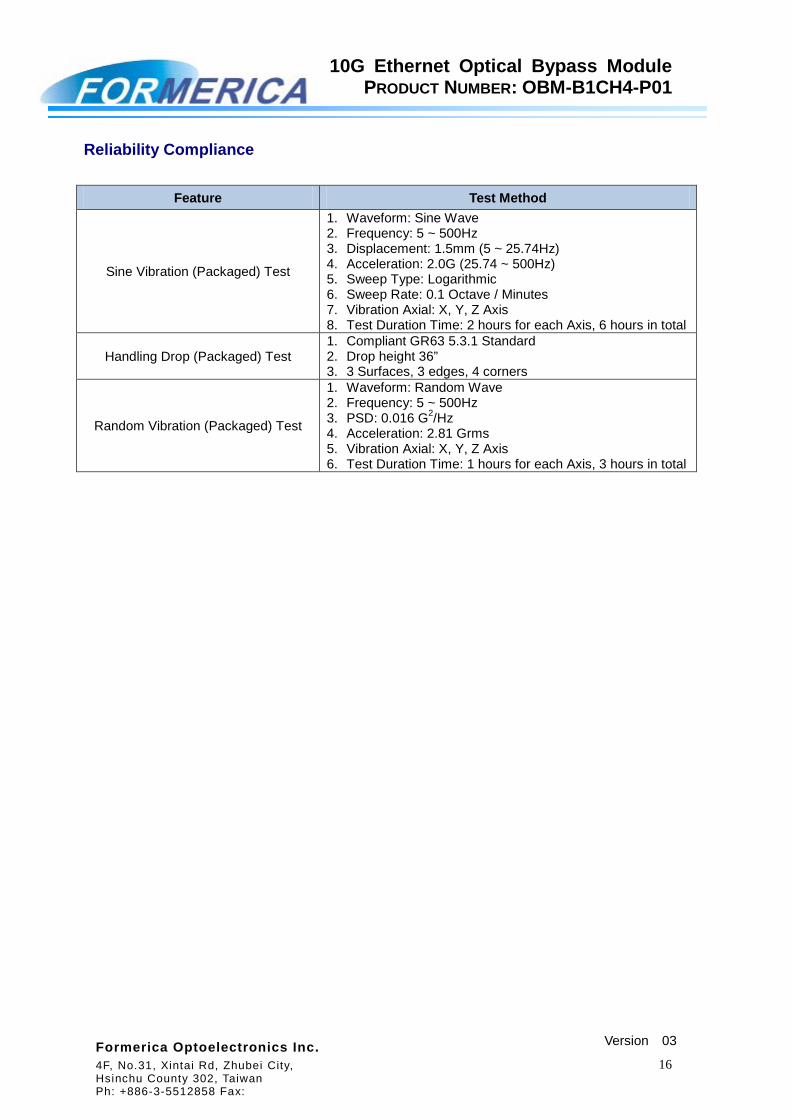
Reliability Compliance
Feature Test Method
Sine Vibration (Packaged) Test
1. Waveform: Sine Wave 2. Frequency: 5 ~ 500Hz 3. Displacement: 1.5mm (5 ~ 25.74Hz) 4. Acceleration: 2.0G (25.74 ~ 500Hz) 5. Sweep Type: Logarithmic 6. Sweep Rate: 0.1 Octave / Minutes 7. Vibration Axial: X, Y, Z Axis 8. Test Duration Time: 2 hours for each Axis, 6 hours in total
Handling Drop (Packaged) Test 1. Compliant GR63 5.3.1 Standard 2. Drop height 36” 3. 3 Surfaces, 3 edges, 4 corners
Random Vibration (Packaged) Test
1. Waveform: Random Wave 2. Frequency: 5 ~ 500Hz 3. PSD: 0.016 G2/Hz 4. Acceleration: 2.81 Grms 5. Vibration Axial: X, Y, Z Axis 6. Test Duration Time: 1 hours for each Axis, 3 hours in total
Related Documents


