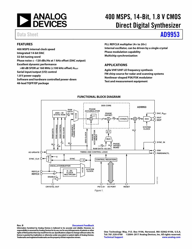
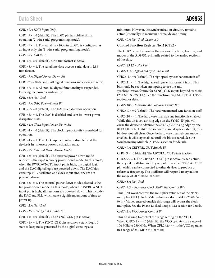
400 MSPS, 14-Bit, 1.8 V CMOS Direct Digital Synthesizer Data Sheet AD9953 Rev. B Document Feedback Information furnished by Analog Devices is believed to be accurate and reliable. However, no responsibility is assumed by Analog Devices for its use, nor for any infringements of patents or other rights of third parties that may result from its use. Specifications subject to change without notice. No license is granted by implication or otherwise under any patent or patent rights of Analog Devices. Trademarks and registered trademarks are the property of their respective owners. One Technology Way, P.O. Box 9106, Norwood, MA 02062-9106, U.S.A. Tel: 781.329.4700 ©2004–2017 Analog Devices, Inc. All rights reserved. Technical Support www.analog.com FEATURES 400 MSPS internal clock speed Integrated 14-bit DAC 32-bit tuning word Phase noise ≤ –120 dBc/Hz at 1 kHz offset (DAC output) Excellent dynamic performance >80 dB SFDR at 160 MHz (±100 kHz offset) AOUT Serial input/output (I/O) control 1.8 V power supply Software and hardware controlled power-down 48-lead TQFP/EP package PLL REFCLK multiplier (4× to 20×) Internal oscillator, can be driven by a single crystal Phase modulation capability Multichip synchronization APPLICATIONS Agile VHF/UHF LO frequency synthesis FM chirp source for radar and scanning systems Nonlinear-shaped PSK/FSK modulator Test and measurement equipment FUNCTIONAL BLOCK DIAGRAM 1024 32 STATIC RAM COS(X) CONTROL REGISTERS OSCILLATOR/BUFFER SYNC ENABLE I/O UPDATE DAC_R SET DDS CORE PHASE OFFSET PHASE ACCUMULATOR Z –1 Z –1 IOUT IOUT OSK PWRDWNCTL REFCLK REFCLK CRYSTAL OUT I/O PORT PS<1:0> RAM DATA <31:18> RAM DATA FREQUENCY TUNING WORD RAM DATA DDS CLOCK DDS CLOCK PHASE ACCUMULATOR RESET DAC MUX SYSTEM CLOCK SYSTEM CLOCK SYNC_IN PHASE OFFSET WORD SYNC_CLK RESET TIMING AND CONTROL LOGIC 4–20 CLOCK MULTIPLIER ÷ 4 AD9953 32 14 14 14 32 R A M A D D R E S S 10 RAM CONTROL 3 19 14 0 32 M U X M U X M U X 03357-0-001 Figure 1.

Welcome message from author
This document is posted to help you gain knowledge. Please leave a comment to let me know what you think about it! Share it to your friends and learn new things together.
Transcript
400 MSPS, 14-Bit, 1.8 V CMOS Direct Digital Synthesizer
Data Sheet AD9953
Rev. B Document Feedback Information furnished by Analog Devices is believed to be accurate and reliable. However, no responsibility is assumed by Analog Devices for its use, nor for any infringements of patents or other rights of third parties that may result from its use. Specifications subject to change without notice. No license is granted by implication or otherwise under any patent or patent rights of Analog Devices. Trademarks and registered trademarks are the property of their respective owners.
One Technology Way, P.O. Box 9106, Norwood, MA 02062-9106, U.S.A.Tel: 781.329.4700 ©2004–2017 Analog Devices, Inc. All rights reserved. Technical Support www.analog.com
FEATURES 400 MSPS internal clock speed Integrated 14-bit DAC 32-bit tuning word Phase noise ≤ –120 dBc/Hz at 1 kHz offset (DAC output) Excellent dynamic performance
>80 dB SFDR at 160 MHz (±100 kHz offset) AOUT Serial input/output (I/O) control 1.8 V power supply Software and hardware controlled power-down 48-lead TQFP/EP package
PLL REFCLK multiplier (4× to 20×) Internal oscillator, can be driven by a single crystal Phase modulation capability Multichip synchronization
APPLICATIONS Agile VHF/UHF LO frequency synthesis FM chirp source for radar and scanning systems Nonlinear-shaped PSK/FSK modulator Test and measurement equipment
FUNCTIONAL BLOCK DIAGRAM
1024 32STATIC RAM
COS(X)
CONTROL REGISTERS
OSCILLATOR/BUFFER
SYNC
ENABLE
I/O UPDATE
DAC_RSET
DDS CORE
PHASEOFFSET
PHASEACCUMULATOR
Z–1
Z–1
IOUTIOUT
OSKPWRDWNCTL
REFCLKREFCLK
CRYSTAL OUT I/O PORTPS<1:0>
RAM DATA <31:18>
RAMDATA
FREQ
UEN
CY
TUN
ING
WO
RD
RA
M D
ATA
DD
S C
LOC
K
DD
S C
LOC
K
PHA
SEA
CC
UM
ULA
TOR
RES
ET
DAC
MUX
SYSTEMCLOCK
SYSTEMCLOCK
SYNC_INPHASEOFFSETWORD
SYNC_CLK
RESET
TIMING AND CONTROL LOGIC
4–20CLOCK
MULTIPLIER
÷ 4
AD9953
32
14
141432
RA
M A
DD
RES
S
10
RA
M C
ON
TRO
L
3
19 14
0
32
MUX
MUX
MUX
0335
7-0-
001
Figure 1.
AD9953 Data Sheet
Rev. B | Page 2 of 32
TABLE OF CONTENTS Features .............................................................................................. 1 Applications ....................................................................................... 1 Revision History ............................................................................... 2 General Description ......................................................................... 3 Electrical Specifications ................................................................... 4 Absolute Maximum Ratings ............................................................ 6
ESD Caution .................................................................................. 6 Pin Configuration ............................................................................. 7 Pin Function Descriptions .............................................................. 8 Typical Performance Characteristics ............................................. 9 Theory of Operation ...................................................................... 12
Component Blocks ..................................................................... 12 Modes of Operation ................................................................... 19 Programming AD9953 Features .............................................. 22 Serial Port Operation ................................................................. 25 Instruction Byte .......................................................................... 27 Serial Interface Port Pin Description ....................................... 27 MSB/LSB Transfers .................................................................... 27
Suggested Application Circuits ..................................................... 29 Outline Dimensions ....................................................................... 30
Ordering Guide .......................................................................... 30
REVISION HISTORY1/2017—Rev. A to Rev. B Changes to Features Section............................................................ 1 Changes to Ordering Guide .......................................................... 30 5/2009—Rev. 0 to Rev. A Changes to Absolute Maximum Ratings Section ......................... 6 Changes to Table 3 ............................................................................ 8 Changes to Table 5 .......................................................................... 14
Changes to Figure 22 ...................................................................... 25 Changes to Serial Port Operation Section .................................. 25 Changes to Serial Interface Port Pin Description Section ........ 27 Changes to Figure 29 ...................................................................... 29 Updated Outline Dimensions ....................................................... 30 Changes to Ordering Guide .......................................................... 30 1/2004—Revision 0: Initial Version
Data Sheet AD9953
Rev. B | Page 3 of 32
GENERAL DESCRIPTION The AD9953 is a direct digital synthesizer (DDS) featuring a 14-bit DAC operating up to 400 MSPS. The AD9953 uses advanced DDS technology, coupled with an internal high speed, high performance DAC to form a digitally programmable, complete high frequency synthesizer capable of generating a frequency-agile analog output sinusoidal waveform at up to 200 MHz. The AD9953 includes an integrated 1024 × 32 static RAM to support flexible frequency sweep capability in several
modes. The AD9953 is designed to provide fast frequency hopping and fine tuning resolution (32-bit frequency tuning word). The frequency tuning and control words are loaded into the AD9953 via a serial I/O port.
The AD9953 is specified to operate over the extended industrial temperature range of –40°C to +105°C.
AD9953 Data Sheet
Rev. B | Page 4 of 32
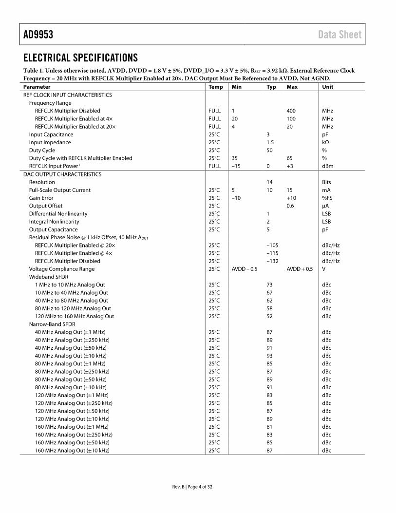
ELECTRICAL SPECIFICATIONS Table 1. Unless otherwise noted, AVDD, DVDD = 1.8 V ± 5%, DVDD_I/O = 3.3 V ± 5%, RSET = 3.92 kΩ, External Reference Clock Frequency = 20 MHz with REFCLK Multiplier Enabled at 20×. DAC Output Must Be Referenced to AVDD, Not AGND.Parameter Temp Min Typ Max Unit REF CLOCK INPUT CHARACTERISTICS
Frequency Range REFCLK Multiplier Disabled FULL 1 400 MHz REFCLK Multiplier Enabled at 4× FULL 20 100 MHz REFCLK Multiplier Enabled at 20× FULL 4 20 MHz
Input Capacitance 25°C 3 pF Input Impedance 25°C 1.5 kΩ Duty Cycle 25°C 50 % Duty Cycle with REFCLK Multiplier Enabled 25°C 35 65 % REFCLK Input Power1 FULL –15 0 +3 dBm
DAC OUTPUT CHARACTERISTICS Resolution 14 Bits Full-Scale Output Current 25°C 5 10 15 mA Gain Error 25°C –10 +10 %FS Output Offset 25°C 0.6 µA Differential Nonlinearity 25°C 1 LSB Integral Nonlinearity 25°C 2 LSB Output Capacitance 25°C 5 pF Residual Phase Noise @ 1 kHz Offset, 40 MHz AOUT
REFCLK Multiplier Enabled @ 20× 25°C –105 dBc/Hz REFCLK Multiplier Enabled @ 4× 25°C –115 dBc/Hz REFCLK Multiplier Disabled 25°C –132 dBc/Hz
Voltage Compliance Range 25°C AVDD – 0.5 AVDD + 0.5 V Wideband SFDR
1 MHz to 10 MHz Analog Out 25°C 73 dBc 10 MHz to 40 MHz Analog Out 25°C 67 dBc 40 MHz to 80 MHz Analog Out 25°C 62 dBc 80 MHz to 120 MHz Analog Out 25°C 58 dBc 120 MHz to 160 MHz Analog Out 25°C 52 dBc
Narrow-Band SFDR 40 MHz Analog Out (±1 MHz) 25°C 87 dBc 40 MHz Analog Out (±250 kHz) 25°C 89 dBc 40 MHz Analog Out (±50 kHz) 25°C 91 dBc 40 MHz Analog Out (±10 kHz) 25°C 93 dBc 80 MHz Analog Out (±1 MHz) 25°C 85 dBc 80 MHz Analog Out (±250 kHz) 25°C 87 dBc 80 MHz Analog Out (±50 kHz) 25°C 89 dBc 80 MHz Analog Out (±10 kHz) 25°C 91 dBc 120 MHz Analog Out (±1 MHz) 25°C 83 dBc 120 MHz Analog Out (±250 kHz) 25°C 85 dBc 120 MHz Analog Out (±50 kHz) 25°C 87 dBc 120 MHz Analog Out (±10 kHz) 25°C 89 dBc 160 MHz Analog Out (±1 MHz) 25°C 81 dBc 160 MHz Analog Out (±250 kHz) 25°C 83 dBc 160 MHz Analog Out (±50 kHz) 25°C 85 dBc 160 MHz Analog Out (±10 kHz) 25°C 87 dBc
Data Sheet AD9953
Rev. B | Page 5 of 32
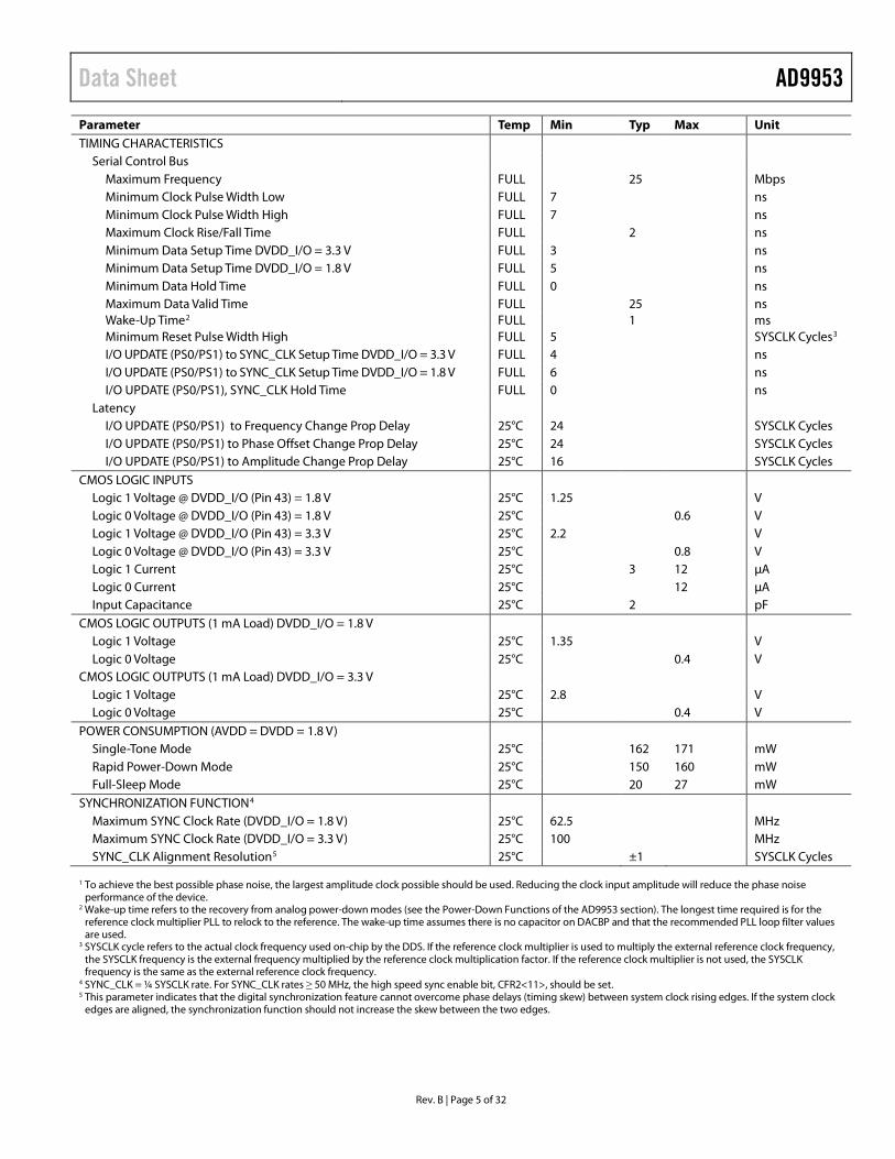
Parameter Temp Min Typ Max Unit TIMING CHARACTERISTICS
Serial Control Bus Maximum Frequency FULL 25 Mbps Minimum Clock Pulse Width Low FULL 7 ns Minimum Clock Pulse Width High FULL 7 ns Maximum Clock Rise/Fall Time FULL 2 ns Minimum Data Setup Time DVDD_I/O = 3.3 V FULL 3 ns Minimum Data Setup Time DVDD_I/O = 1.8 V FULL 5 ns Minimum Data Hold Time FULL 0 ns Maximum Data Valid Time FULL 25 ns Wake-Up Time2 FULL 1 ms Minimum Reset Pulse Width High FULL 5 SYSCLK Cycles3 I/O UPDATE (PS0/PS1) to SYNC_CLK Setup Time DVDD_I/O = 3.3 V FULL 4 ns I/O UPDATE (PS0/PS1) to SYNC_CLK Setup Time DVDD_I/O = 1.8 V FULL 6 ns I/O UPDATE (PS0/PS1), SYNC_CLK Hold Time FULL 0 ns
Latency I/O UPDATE (PS0/PS1) to Frequency Change Prop Delay 25°C 24 SYSCLK Cycles I/O UPDATE (PS0/PS1) to Phase Offset Change Prop Delay 25°C 24 SYSCLK Cycles I/O UPDATE (PS0/PS1) to Amplitude Change Prop Delay 25°C 16 SYSCLK Cycles
CMOS LOGIC INPUTS Logic 1 Voltage @ DVDD_I/O (Pin 43) = 1.8 V 25°C 1.25 V Logic 0 Voltage @ DVDD_I/O (Pin 43) = 1.8 V 25°C 0.6 V Logic 1 Voltage @ DVDD_I/O (Pin 43) = 3.3 V 25°C 2.2 V Logic 0 Voltage @ DVDD_I/O (Pin 43) = 3.3 V 25°C 0.8 V Logic 1 Current 25°C 3 12 µA Logic 0 Current 25°C 12 µA Input Capacitance 25°C 2 pF
CMOS LOGIC OUTPUTS (1 mA Load) DVDD_I/O = 1.8 V Logic 1 Voltage 25°C 1.35 V Logic 0 Voltage 25°C 0.4 V
CMOS LOGIC OUTPUTS (1 mA Load) DVDD_I/O = 3.3 V Logic 1 Voltage 25°C 2.8 V Logic 0 Voltage 25°C 0.4 V
POWER CONSUMPTION (AVDD = DVDD = 1.8 V) Single-Tone Mode 25°C 162 171 mW Rapid Power-Down Mode 25°C 150 160 mW Full-Sleep Mode 25°C 20 27 mW
SYNCHRONIZATION FUNCTION4 Maximum SYNC Clock Rate (DVDD_I/O = 1.8 V) 25°C 62.5 MHz Maximum SYNC Clock Rate (DVDD_I/O = 3.3 V) 25°C 100 MHz SYNC_CLK Alignment Resolution5 25°C ±1 SYSCLK Cycles
1 To achieve the best possible phase noise, the largest amplitude clock possible should be used. Reducing the clock input amplitude will reduce the phase noise
performance of the device. 2 Wake-up time refers to the recovery from analog power-down modes (see the Power-Down Functions of the AD9953 section). The longest time required is for the
reference clock multiplier PLL to relock to the reference. The wake-up time assumes there is no capacitor on DACBP and that the recommended PLL loop filter values are used.
3 SYSCLK cycle refers to the actual clock frequency used on-chip by the DDS. If the reference clock multiplier is used to multiply the external reference clock frequency, the SYSCLK frequency is the external frequency multiplied by the reference clock multiplication factor. If the reference clock multiplier is not used, the SYSCLK frequency is the same as the external reference clock frequency.
4 SYNC_CLK = ¼ SYSCLK rate. For SYNC_CLK rates ≥ 50 MHz, the high speed sync enable bit, CFR2<11>, should be set. 5 This parameter indicates that the digital synchronization feature cannot overcome phase delays (timing skew) between system clock rising edges. If the system clock
edges are aligned, the synchronization function should not increase the skew between the two edges.
AD9953 Data Sheet
Rev. B | Page 6 of 32
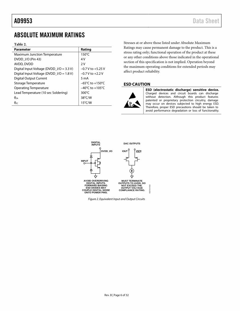
ABSOLUTE MAXIMUM RATINGS Table 2. Parameter Rating Maximum Junction Temperature 150°C DVDD_I/O (Pin 43) 4 V AVDD, DVDD 2 V Digital Input Voltage (DVDD_I/O = 3.3 V) –0.7 V to +5.25 V Digital Input Voltage (DVDD_I/O = 1.8 V) –0.7 V to +2.2 V Digital Output Current 5 mA Storage Temperature –65°C to +150°C
Operating Temperature –40°C to +105°C Lead Temperature (10 sec Soldering) 300°C θJA 38°C/W
θJC 15°C/W
Stresses at or above those listed under Absolute Maximum Ratings may cause permanent damage to the product. This is a stress rating only; functional operation of the product at these or any other conditions above those indicated in the operational section of this specification is not implied. Operation beyond the maximum operating conditions for extended periods may affect product reliability.
ESD CAUTION
IOUT IOUT
MUST TERMINATEOUTPUTS TO AVDD. DO
NOT EXCEED THEOUTPUT VOLTAGE
COMPLIANCE RATING.
DAC OUTPUTS
DVDD_I/O
INPUT
DIGITALINPUTS
AVOID OVERDRIVINGDIGITAL INPUTS.
FORWARD BIASINGESD DIODES MAY
COUPLE DIGITAL NOISEONTO POWER PINS. 03
374-
0-03
2
Figure 2. Equivalent Input and Output Circuits
Data Sheet AD9953
Rev. B | Page 7 of 32
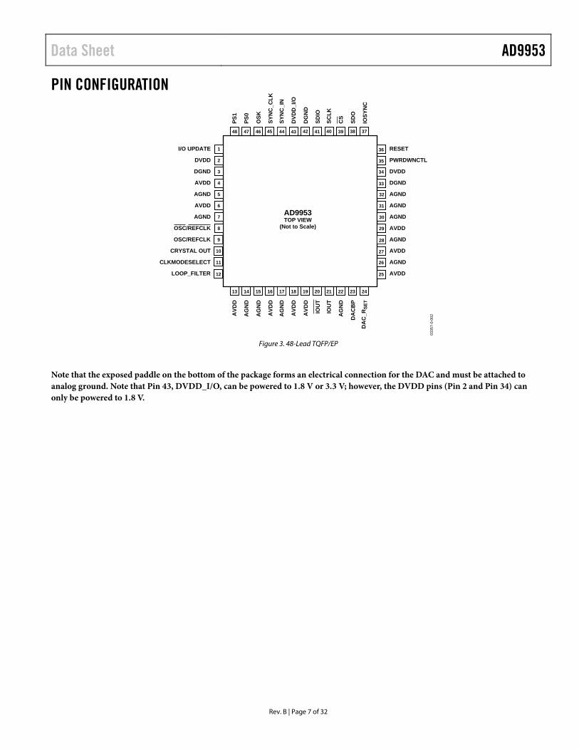
PIN CONFIGURATION
43 42 41 40 39 38 3748 47 46 45 44
13 15 16 17 18 19 20 21 22 23 24
I/O UPDATE
DVDD
DGND
AVDD
AGND
AVDD
AGND
OSC/REFCLK
OSC/REFCLK
CRYSTAL OUT
CLKMODESELECT
LOOP_FILTER
AG
ND
AVD
D
AG
ND
AVD
D
AG
ND
AVD
D
IOU
T
AVD
D
IOU
T
DA
CB
P
AG
ND
OSK
PS1
PS0
SYN
C_C
LK
SYN
C_I
N
DVD
D_I
/O
SCLK
DG
ND
SDIO
SDO
CS
IOSY
NC
RESET
PWRDWNCTL
DVDD
DGND
AGND
AGND
AGND
AVDD
AGND
AVDD
AGND
AVDD
AD9953TOP VIEW
(Not to Scale)
14
1
2
3
4
5
6
7
8
9
10
11
12
36
35
34
33
32
31
30
29
28
27
26
25
0335
7-0-
002
DA
C_R
SET
Figure 3. 48-Lead TQFP/EP
Note that the exposed paddle on the bottom of the package forms an electrical connection for the DAC and must be attached to analog ground. Note that Pin 43, DVDD_I/O, can be powered to 1.8 V or 3.3 V; however, the DVDD pins (Pin 2 and Pin 34) can only be powered to 1.8 V.
AD9953 Data Sheet
Rev. B | Page 8 of 32
PIN FUNCTION DESCRIPTIONS Table 3. 48-Lead TQFP/EP Pin No. Mnemonic I/O Description 1 I/O UPDATE I The rising edge transfers the contents of the internal buffer memory to the I/O registers. This pin
must be set up and held around the SYNC_CLK output signal. 2, 34 DVDD I Digital Power Supply Pins (1.8 V). 3, 33, 42 DGND I Digital Power Ground Pins. 4, 6, 13, 16, 18, 19, 25, 27, 29
AVDD I Analog Power Supply Pins (1.8 V).
5, 7, 14, 15, 17, 22, 26, 32
AGND I Analog Power Ground Pins.
8 OSC/ REFCLK I Complementary Reference Clock/Oscillator Input. When the REFCLK port is operated in single-ended mode, REFCLK should be decoupled to AVDD with a 0.1 µF capacitor.
9 OSC/REFCLK I Reference Clock/Oscillator Input. See Clock Input section for details on the OSCILLATOR/REFCLK operation.
10 CRYSTAL OUT O Output of the Oscillator Section. 11 CLKMODESELECT I Control Pin for the Oscillator Section. When high, the oscillator section is enabled. When low, the
oscillator section is bypassed. 12 LOOP_FILTER I This pin provides the connection for the external zero compensation network of the REFCLK
multiplier’s PLL loop filter. The network consists of a 1 kΩ resistor in series with a 0.1 µF capacitor tied to AVDD.
20 IOUT O Complementary DAC Output. Should be biased through a resistor to AVDD, not AGND.
21 IOUT O DAC Output. Should be biased through a resistor to AVDD, not AGND. 23 DACBP I DAC Biasline Decoupling Pin. A 0.1 μF capacitor to AGND is recommended. 24 DAC_RSET I A resistor (3.92 kΩ nominal) connected from AGND to DAC_RSET establishes the reference current
for the DAC. 35 PWRDWNCTL I Input Pin Used as an External Power-Down Control (see Table 10 for details). 36 RESET I Active High Hardware Reset Pin. Assertion of the RESET pin forces the AD9953 to the initial state,
as described in the I/O port register map. 37 IOSYNC I Asynchronous Active High Reset of the Serial Port Controller. When high, the current I/O
operation is immediately terminated, enabling a new I/O operation to commence once IOSYNC is returned low. If unused, ground this pin; do not allow this pin to float.
38 SDO O When operating the I/O port as a 3-wire serial port, this pin serves as the serial data output. When operated as a 2-wire serial port, this pin is unused and can be left unconnected.
39 CS I This pin functions as an active low chip select that allows multiple devices to share the I/O bus.
40 SCLK I This pin functions as the serial data clock for I/O operations. 41 SDIO I/O When operating the I/O port as a 3-wire serial port, this pin serves as the serial data input only.
When operated as a 2-wire serial port, this pin is the bidirectional serial data pin. 43 DVDD_I/O I Digital Power Supply (for I/O Cells Only, 3.3 V). 44 SYNC_IN I Input Signal Used to Synchronize Multiple AD9953s. This input is connected to the SYNC_CLK
output of a master AD9953. 45 SYNC_CLK O Clock Output Pin that Serves as a Synchronizer for External Hardware. 46 OSK I Input Pin Used to Control the Direction of the Shaped On-Off Keying Function when Programmed
for Operation. OSK is synchronous to the SYNC_CLK pin. When OSK is not programmed, this pin should be tied to DGND.
47, 48 PS0, PS1 I Input pin used to select one of the four internal profiles. Profile <1:0> are synchronous to the SYNC_CLK pin. Any change in these inputs transfers the contents of the internal buffer memory to the I/O registers (sends an internal I/O UPDATE).
<49> AGND I The exposed paddle on the bottom of the package is a ground connection for the DAC and must be attached to AGND in any board layout.
Data Sheet AD9953
Rev. B | Page 9 of 32
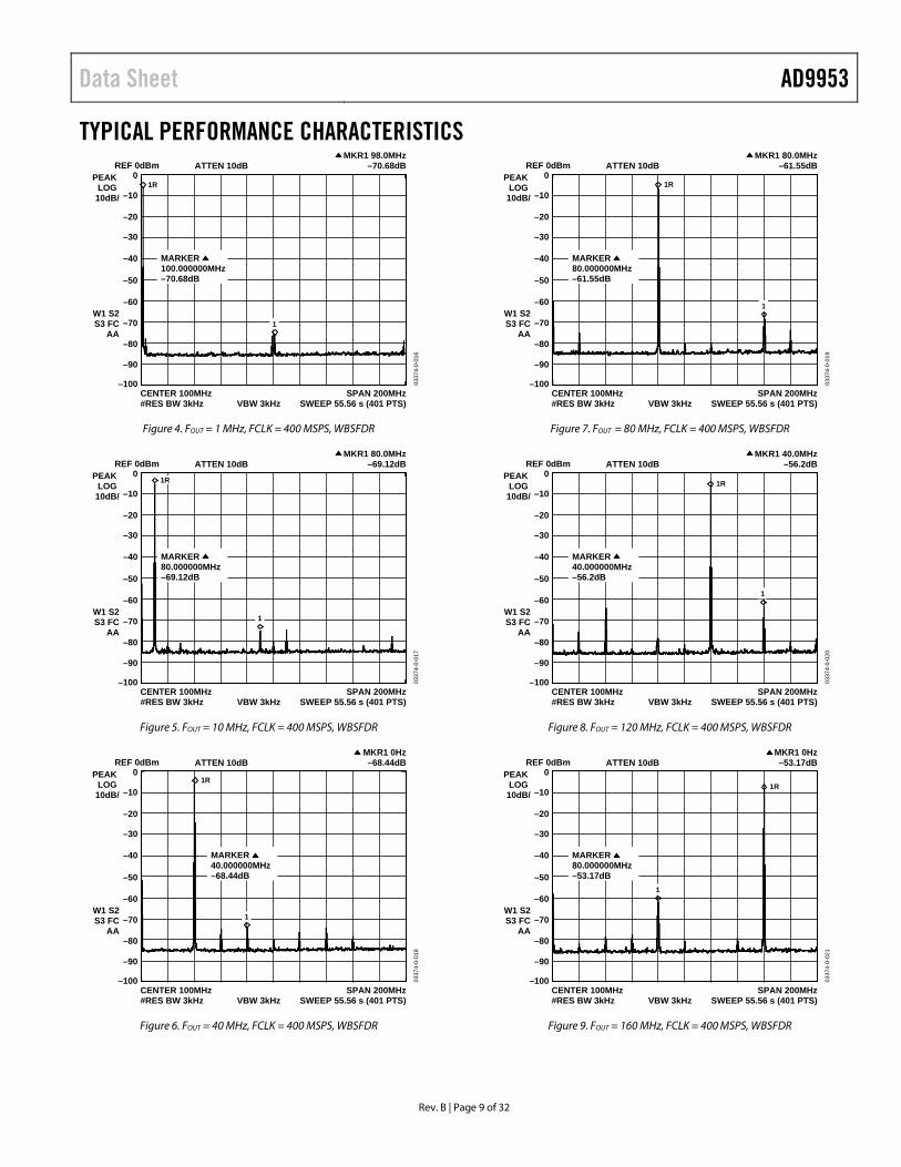
TYPICAL PERFORMANCE CHARACTERISTICS
CENTER 100MHz#RES BW 3kHz
–100
–90
–80
–70
–60
–50
–40
–30
–20
–10
0
VBW 3kHzSPAN 200MHz
SWEEP 55.56 s (401 PTS)
W1 S2S3 FC
AA
REF 0dBmPEAK
LOG10dB/
ATTEN 10dBMKR1 98.0MHz
–70.68dB
1
1R
0337
4-0-
016
MARKER100.000000MHz–70.68dB
Figure 4. FOUT = 1 MHz, FCLK = 400 MSPS, WBSFDR
CENTER 100MHz#RES BW 3kHz
–100
–90
–80
–70
–60
–50
–40
–30
–20
–10
0
VBW 3kHzSPAN 200MHz
SWEEP 55.56 s (401 PTS)
W1 S2S3 FC
AA
REF 0dBmPEAK
LOG10dB/
ATTEN 10dBMKR1 80.0MHz
–69.12dB
1
1R
0337
4-0-
017
MARKER80.000000MHz–69.12dB
Figure 5. FOUT = 10 MHz, FCLK = 400 MSPS, WBSFDR
CENTER 100MHz#RES BW 3kHz
–100
–90
–80
–70
–60
–50
–40
–30
–20
–10
0
VBW 3kHzSPAN 200MHz
SWEEP 55.56 s (401 PTS)
W1 S2S3 FC
AA
REF 0dBmPEAK
LOG10dB/
ATTEN 10dBMKR1 0Hz–68.44dB
1
1R
0337
4-0-
018
MARKER40.000000MHz–68.44dB
Figure 6. FOUT = 40 MHz, FCLK = 400 MSPS, WBSFDR
CENTER 100MHz#RES BW 3kHz
–100
–90
–80
–70
–60
–50
–40
–30
–20
–10
0
VBW 3kHzSPAN 200MHz
SWEEP 55.56 s (401 PTS)
W1 S2S3 FC
AA
REF 0dBmPEAK
LOG10dB/
ATTEN 10dBMKR1 80.0MHz
–61.55dB
1
1R
0337
4-0-
019
MARKER80.000000MHz–61.55dB
Figure 7. FOUT = 80 MHz, FCLK = 400 MSPS, WBSFDR
CENTER 100MHz#RES BW 3kHz
–100
–90
–80
–70
–60
–50
–40
–30
–20
–10
0
VBW 3kHzSPAN 200MHz
SWEEP 55.56 s (401 PTS)
W1 S2S3 FC
AA
REF 0dBmPEAK
LOG10dB/
ATTEN 10dBMKR1 40.0MHz
–56.2dB
1
1R
0337
4-0-
020
MARKER40.000000MHz–56.2dB
Figure 8. FOUT = 120 MHz, FCLK = 400 MSPS, WBSFDR
CENTER 100MHz#RES BW 3kHz
–100
–90
–80
–70
–60
–50
–40
–30
–20
–10
0
VBW 3kHzSPAN 200MHz
SWEEP 55.56 s (401 PTS)
W1 S2S3 FC
AA
REF 0dBmPEAK
LOG10dB/
ATTEN 10dBMKR1 0Hz–53.17dB
1
1R
0337
4-0-
021
MARKER80.000000MHz–53.17dB
Figure 9. FOUT = 160 MHz, FCLK = 400 MSPS, WBSFDR
AD9953 Data Sheet
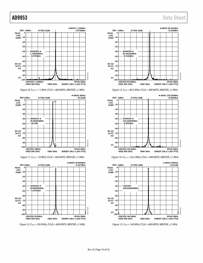
Rev. B | Page 10 of 32
CENTER 1.105MHz#RES BW 30Hz
–100
–90
–80
–70
–60
–50
–40
–30
–20
–10
0
VBW 30HzSPAN 2MHz
SWEEP 199.2 s (401 PTS)
W1 S2S3 FC
AA
ST
REF –4dBmPEAK
LOG10dB/
ATTEN 10dBMKR1 1.105MHz
–5.679dBm1
0337
4-0-
022
MARKER1.105000MHz–5.679dBm
Figure 10. FOUT = 1.1 MHz, FCLK = 400 MSPS, NBSFDR, ±1 MHz
CENTER 10MHz#RES BW 30Hz
–100
–90
–80
–70
–60
–50
–40
–30
–20
–10
0
VBW 30HzSPAN 2MHz
SWEEP 199.2 s (401 PTS)
W1 S2S3 FC
AA
REF 0dBmPEAK
LOG10dB/
ATTEN 10dBMKR1 85kHz
–93.01dB
1
1R
0337
4-0-
023
MARKER40.000000MHz–56.2dB
Figure 11. FOUT = 10 MHz, FCLK = 400 MSPS, NBSFDR, ±1 MHz
CENTER 39.9MHz#RES BW 30Hz
–100
–90
–80
–70
–60
–50
–40
–30
–20
–10
0
VBW 30HzSPAN 2MHz
SWEEP 199.2 s (401 PTS)
W1 S2S3 FC
AA
REF 0dBmPEAK
LOG10dB/
ATTEN 10dBMKR1 39.905MHz
–5.347dBm1
0337
4-0-
024
MARKER39.905000MHz–5.347dBm
Figure 12. FOUT = 39.9 MHz, FCLK = 400 MSPS, NBSFDR, ±1 MHz
CENTER 80.25MHz#RES BW 30Hz
–100
–90
–80
–70
–60
–50
–40
–30
–20
–10
0
VBW 30HzSPAN 2MHz
SWEEP 199.2 s (401 PTS)
W1 S2S3 FC
AA
ST
REF –4dBmPEAK
LOG10dB/
ATTEN 10dBMKR1 80.301MHz
–6.318dBm1
0337
4-0-
025
MARKER80.301000MHz–6.318dBm
Figure 13. FOUT = 80.3 MHz, FCLK = 400 MSPS, NBSFDR, ±1 MHz
CENTER 120.2MHz#RES BW 30Hz
–100
–90
–80
–70
–60
–50
–40
–30
–20
–10
0
VBW 30HzSPAN 2MHz
SWEEP 199.2 s (401 PTS)
W1 S2S3 FC
AA
ST
REF –4dBmPEAK
LOG10dB/
ATTEN 10dBMKR1 120.205MHz
–6.825dBm1
0337
4-0-
026
MARKER120.205000MHz–6.825dBm
Figure 14. FOUT = 120.2 MHz, FCLK = 400 MSPS, NBSFDR, ±1 MHz
CENTER 160.5MHz#RES BW 30Hz
–100
–90
–80
–70
–60
–50
–40
–30
–20
–10
0
VBW 30HzSPAN 2MHz
SWEEP 199.2 s (401 PTS)
W1 S2S3 FC
AA
ST
REF –4dBmPEAK
LOG10dB/
ATTEN 10dBMKR1 600kHz
–0.911dB1
0337
4-0-
027
CENTER160.5000000MHz
Figure 15. FOUT = 160 MHz, FCLK = 400 MSPS, NBSFDR, ±1 MHz
Data Sheet AD9953
Rev. B | Page 11 of 32
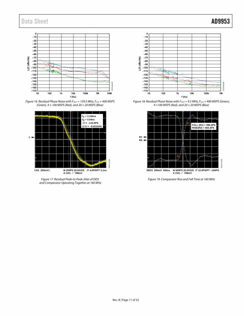
Figure 16. Residual Phase Noise with FOUT = 159.5 MHz, FCLK = 400 MSPS (Green), 4 × 100 MSPS (Red), and 20 × 20 MSPS (Blue)
CH1 200mV
1
IT 4.0PS/PT 3.1nsM 200PS 20.0GS/SA CH1 708mV
0337
4-0-
031
t1 = 3.156nst2 = 3.04nst = –116.0PS1/t = –8.621GHz
Figure 17. Residual Peak-to-Peak Jitter of DDS and Comparator Operating Together at 160 MHz
Figure 18. Residual Phase Noise with FOUT = 9.5 MHz, FCLK = 400 MSPS (Green), 4 ×100 MSPS (Red), and 20 × 20 MSPS (Blue)
REF2 200mV 500ns
R2R1
IT 10.0PS/PT –100PSM 500PS 20.0GS/SA CH1 708mV
0337
4-0-
030
FALL (R1) = 396.4PSRISE(R2) = 464.3PS
Figure 19. Comparator Rise and Fall Time at 160 MHz
AD9953 Data Sheet
Rev. B | Page 12 of 32
THEORY OF OPERATION COMPONENT BLOCKS DDS Core
The output frequency (fO) of the DDS is a function of the frequency of the system clock (SYSCLK), the value of the frequency tuning word (FTW), and the capacity of the accumulator (232, in this case). The exact relationship is given below with fS defined as the frequency of SYSCLK.
( )( ) 3132 202/ ≤≤= FTWwithfFTWf SO
( )( ) 1–222/–1 323132 <<×= FTWwithFTWff SO
The value at the output of the phase accumulator is translated to an amplitude value via the COS(x) functional block and routed to the DAC.
In certain applications, it is desirable to force the output signal to zero phase. Simply setting the FTW to 0 does not accomplish this; it only results in the DDS core holding its current phase value. Thus, a control bit is required to force the phase accumulator output to zero.
At power-up, the clear phase accumulator bit is set to Logic 1, but the buffer memory for this bit is cleared (Logic 0). Therefore, upon power-up, the phase accumulator will remain clear until the first I/O UPDATE is issued.
Phase-Locked Loop (PLL)
The PLL allows multiplication of the REFCLK frequency. Control of the PLL is accomplished by programming the 5-bit REFCLK multiplier portion of Control Function Register No. 2, Bits <7:3>.
When programmed for values ranging from 0x04 to 0x14 (4 decimal to 20 decimal), the PLL multiplies the REFCLK input frequency by the corresponding decimal value. However, the maximum output frequency of the PLL is restricted to 400 MHz. Whenever the PLL value is changed, the user should be aware that time must be allocated to allow the PLL to lock (approximately 1 ms).
The PLL is bypassed by programming a value outside the range of 4 to 20 (decimal). When bypassed, the PLL is shut down to conserve power.
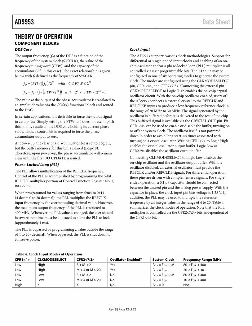
Clock Input
The AD9953 supports various clock methodologies. Support for differential or single-ended input clocks and enabling of an on-chip oscillator and/or a phase-locked loop (PLL) multiplier is all controlled via user programmable bits. The AD9953 may be configured in one of six operating modes to generate the system clock. The modes are configured using the CLKMODESELECT pin, CFR1<4>, and CFR2<7:3>. Connecting the external pin CLKMODESELECT to Logic High enables the on-chip crystal oscillator circuit. With the on-chip oscillator enabled, users of the AD9953 connect an external crystal to the REFCLK and REFCLKB inputs to produce a low frequency reference clock in the range of 20 MHz to 30 MHz. The signal generated by the oscillator is buffered before it is delivered to the rest of the chip. This buffered signal is available via the CRYSTAL OUT pin. Bit CFR1<4> can be used to enable or disable the buffer, turning on or off the system clock. The oscillator itself is not powered down in order to avoid long start-up times associated with turning on a crystal oscillator. Writing CFR2<9> to Logic High enables the crystal oscillator output buffer. Logic Low at CFR2<9> disables the oscillator output buffer.
Connecting CLKMODESELECT to Logic Low disables the on-chip oscillator and the oscillator output buffer. With the oscillator disabled, an external oscillator must provide the REFCLK and/or REFCLKB signals. For differential operation, these pins are driven with complementary signals. For single-ended operation, a 0.1 µF capacitor should be connected between the unused pin and the analog power supply. With the capacitor in place, the clock input pin bias voltage is 1.35 V. In addition, the PLL may be used to multiply the reference frequency by an integer value in the range of 4 to 20. Table 4 summarizes the clock modes of operation. Note that the PLL multiplier is controlled via the CFR2<7:3> bits, independent of the CFR1<4> bit.
Table 4. Clock Input Modes of Operation CFR1<4> CLKMODESELECT CFR2<7:3> Oscillator Enabled? System Clock Frequency Range (MHz) Low High 3 < M < 21 Yes FCLK = FOSC × M 80 < FCLK < 400 Low High M < 4 or M > 20 Yes FCLK = FOSC 20 < FCLK < 30 Low Low 3 < M < 21 No FCLK = FOSC × M 80 < FCLK < 400 Low Low M < 4 or M > 20 No FCLK = FOSC 10 < FCLK < 400 High X X No FCLK = 0 N/A
Data Sheet AD9953
Rev. B | Page 13 of 32
DAC Output
The AD9953 incorporates an integrated 14-bit current output DAC. Unlike most DACs, this output is referenced to AVDD, not AGND.
Two complementary outputs provide a combined full-scale output current (IOUT). Differential outputs reduce the amount of common-mode noise that might be present at the DAC output, offering the advantage of an increased signal-to-noise ratio. The full-scale current is controlled by an external resistor (RSET) connected between the DAC_RSET pin and the DAC ground (AGND_DAC). The full-scale current is proportional to the resistor value as follows:
OUTSET IR /19.39=
The maximum full-scale output current of the combined DAC outputs is 15 mA, but limiting the output to 10 mA provides the best spurious-free dynamic range (SFDR) performance. The DAC output compliance range is AVDD + 0.5 V to AVDD – 0.5 V. Voltages developed beyond this range will cause excessive DAC distortion and could potentially damage the DAC output circuitry. Proper attention should be paid to the load termination to keep the output voltage within this compliance range.
Serial IO Port
The AD9953 serial port is a flexible, synchronous serial communications port that allows easy interface to many industry-standard microcontrollers and microprocessors. The serial I/O port is compatible with most synchronous transfer formats, including both the Motorola 6905/11 SPI® and Intel® 8051 SSR protocols.
The interface allows read/write access to all registers that configure the AD9953. MSB first or LSB first transfer formats are supported. The AD9953’s serial interface port can be configured as a single pin I/O (SDIO), which allows a 2-wire interface or two unidirectional pins for in/out (SDIO/SDO), which in turn enables a 3-wire interface. Two optional pins, IOSYNC and CS, enable greater flexibility for system design in the AD9953.
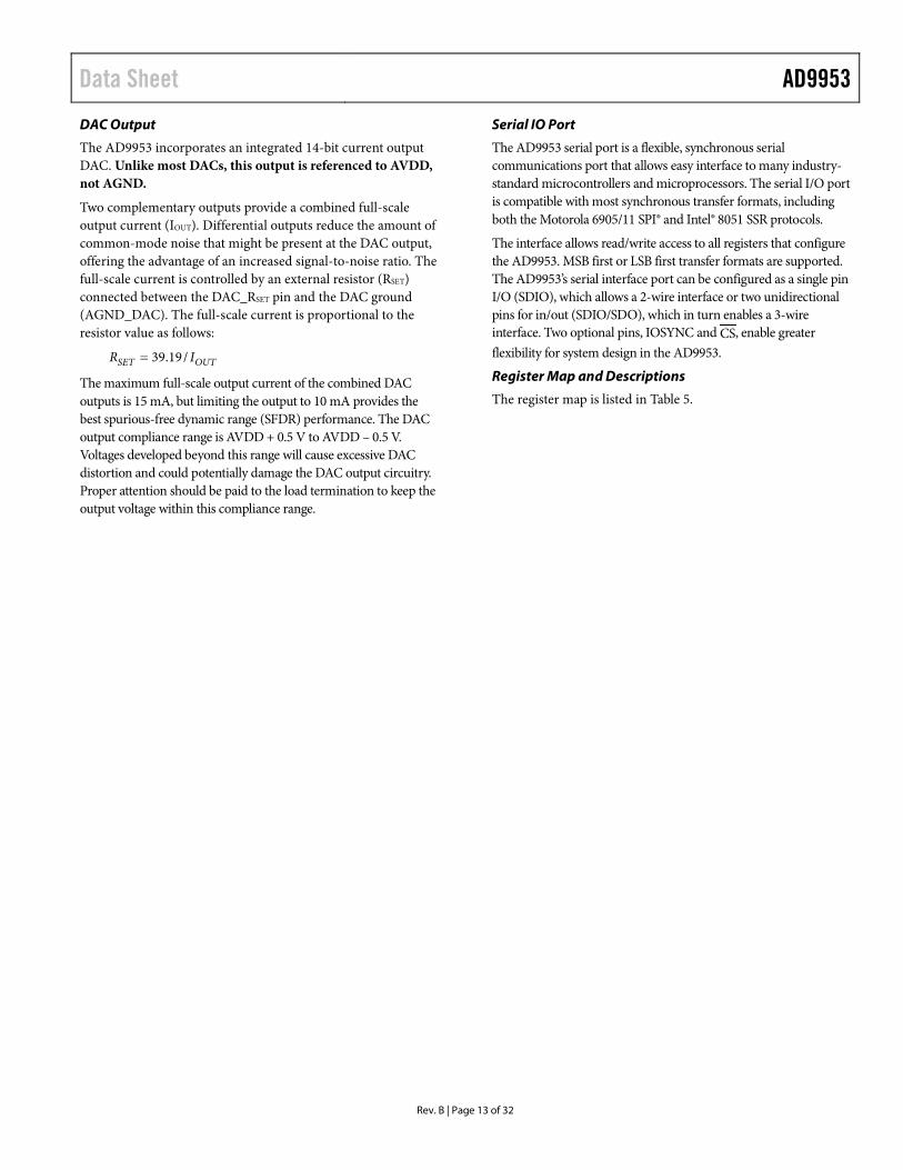
Register Map and Descriptions
The register map is listed in Table 5.
AD9953 Data Sheet
Rev. B | Page 14 of 32
Table 5. Register Map Register Name (Serial Address)
Bit Range
(MSB) Bit 7 Bit 6 Bit 5 Bit 4 Bit 3 Bit 2 Bit 1
(LSB) Bit 0
Default Value OR Profile
Control Function Register
No.1 (CFR1) (0x00)
<7:0> Digital Power-Down
Comp Power-Down
DAC Power-Down
Clock Input Power-Down
External Power-Down Mode
Linear Sweep No
Dwell
SYNC_CLK Out
Disable
Not Used
0x00
<15:8> Load SRR @ I/O UD
AutoClr Freq.
Accum.
AutoClr Phase
Accum.
Enable SINE
Output
Clear Freq.
Accum.
Clear Phase
Accum.
SDIO Input Only
LSB First 0x00
<23:16> Automatic
Sync Enable
Software Manual
Sync
Linear Sweep Enable
Not Used Not Used Not Used Not Used Not Used
0x00
<31:24> RAM Enable
RAM Dest. Is Phase Word
Internal Profile Control <2:0> Load ARR @ I/O UD
OSK Enable
Auto OSK
Keying
0x00
Control Function Register
No. 2 (CFR2) (0x01)
<7:0> REFCLK Multiplier
0x00 or 0x01, or 0x02 or 0x03: Bypass Multiplier 0x04 to 0x14: 4× to 20× Multiplication
VCO Range Charge Pump Current <1:0>
0x00
<15:8> Not Used
High Speed Sync
Enable
Hardware Manual
Sync Enable
CRYSTAL OUT Pin Active
Not Used
0x00
<23:16> Not Used 0x18 Amplitude
Scale Factor (ASF)
(0x02)
<7:0> Amplitude Scale Factor Register <7:0> 0x00
<15:8> Auto Ramp Rate Speed
Control <1:0> Amplitude Scale Factor Register <13:8>
0x00
Amplitude Ramp Rate
(ARR) (0x03)
<7:0> Amplitude Ramp Rate Register <7:0>
0x00
Frequency Tuning Word
(FTW0) (0x04)
<7:0> Frequency Tuning Word No. 0 <7:0> 0x00 <15:8> Frequency Tuning Word No. 0 <15:8> 0x00
<23:16> Frequency Tuning Word No. 0 <23:16> 0x00
<31:24> Frequency Tuning Word No. 0 <31:24> 0x00
Phase Offset Word
(POW0) (0x05)
<7:0> Phase Offset Word No. 0 <7:0> 0x00
<15:8> Not Used<1:0> Phase Offset Word No. 0 <13:8> 0x00
Frequency Tuning Word
(FTW1) (0x06)
<7:0> Frequency Tuning Word No. 1 <7:0> 0x00 <15:8> Frequency Tuning Word No. 1 <15:8> 0x00
<23:16> Frequency Tuning Word No. 1 <23:16> 0x00
<31:24> Frequency Tuning Word No. 1 <31:24> 0x00
Data Sheet AD9953
Rev. B | Page 15 of 32
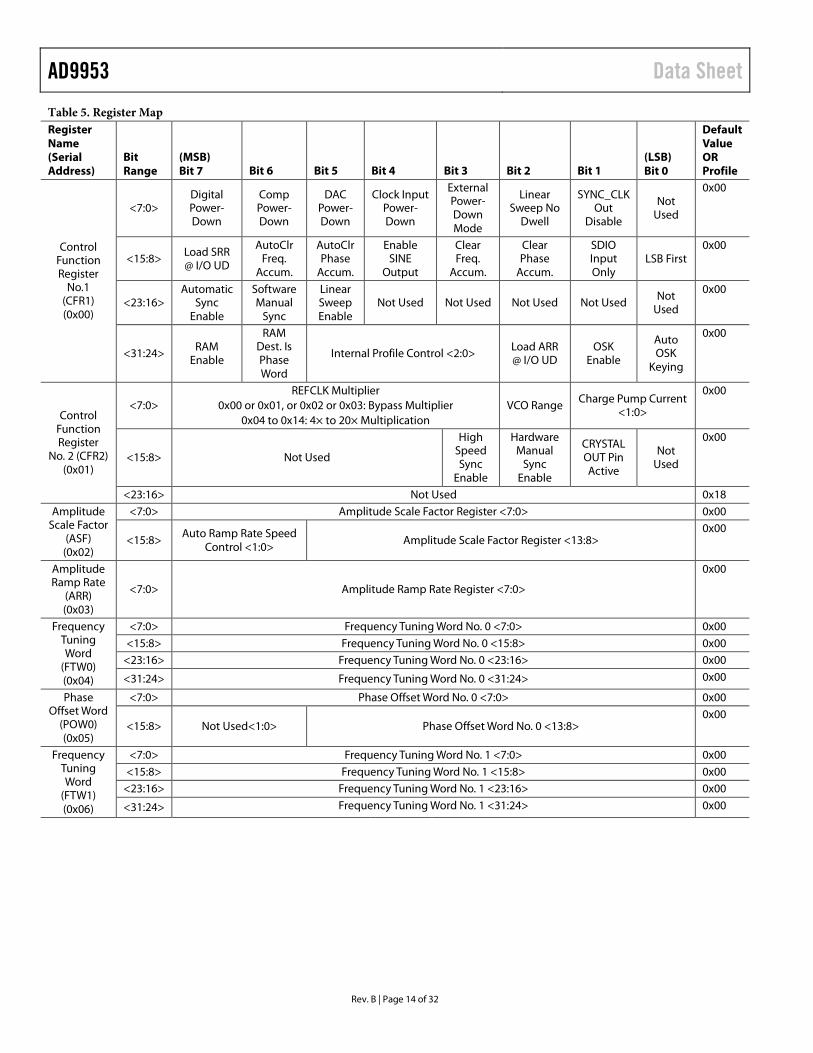
Register Name (Serial Address)
Bit Range
(MSB) Bit 7 Bit 6 Bit 5 Bit 4 Bit 3 Bit 2 Bit 1
(LSB) Bit 0
Default Value OR Profile
RAM Segment Control
Word No. 0 (RSCW0)
(0x07)
<7:0> RAM Segment 0 Mode Control <2:0> No Dwell Active
RAM Segment 0 Beginning Address <9:6> PS0 = 0 PS1 = 0
<15:8> RAM Segment 0 Beginning Address <5:0> RAM Segment 0 Final Address <9:8> PS0 = 0
PS1 = 0
<23:16> RAM Segment 0 Final Address <7:0> PS0 = 0 PS1 = 0
<31:24> RAM Segment 0 Address Ramp Rate <15:8> PS0 = 0
PS1 = 0
<39:32> RAM Segment 0 Address Ramp Rate <7:0> PS0 = 0 PS1 = 0
RAM Segment Control
Word No. 1 (RSCW1)
(0x08)
<7:0> RAM Segment 1 Mode Control
<2:0> No Dwell
Active RAM Segment 1 Beginning Address <9:6> PS0 = 1
PS1 = 0
<15:8> RAM Segment 1 Beginning Address <5:0> RAM Segment 1 Final Address <9:8> PS0 = 1 PS1 = 0
<23:16> RAM Segment 1 Final Address <7:0> PS0 = 1
PS1 = 0
<31:24> RAM Segment 1 Address Ramp Rate <15:8> PS0 = 1 PS1 = 0
<39:32> RAM Segment 1 Address Ramp Rate <7:0> PS0 = 1
PS1 = 0
RAM Segment Control
Word No. 2 (RSCW2)
(0x09)
<7:0> RAM Segment 2 Mode Control <2:0>
No Dwell Active RAM Segment 2 Beginning Address <9:6>
PS0 = 0 PS1 = 1
<15:8> RAM Segment 2 Beginning Address <5:0> RAM Segment 2 Final Address <9:8> PS0 = 0
PS1 = 1
<23:16> RAM Segment 2 Final Address <7:0> PS0 = 0 PS1 = 1
<31:24> RAM Segment 2 Address Ramp Rate <15:8> PS0 = 0
PS1 = 1
<39:32> RAM Segment 2 Address Ramp Rate <7:0> PS0 = 0 PS1 = 1
RAM Segment Control
Word No. 3 (RSCW3)
(0x0A)
<7:0> RAM Segment 3 Mode Control
<2:0> No Dwell Active RAM Segment 3 Beginning
Address <9:6> PS0 = 1 PS1 = 1
<15:8> RAM Segment 3 Beginning Address <5:0> RAM Segment 3 Final Address <9:8> PS0 = 1 PS1 = 1
<23:16> RAM Segment 3 Final Address <7:0> PS0 = 1
PS1 = 1
<31:24> RAM Segment 3 Address Ramp Rate <15:8> PS0 = 1 PS1 = 1
<39:32> RAM Segment 3 Address Ramp Rate <7:0> PS0 = 1
PS1 = 1 RAM (0x0B) RAM [1023:0] <31:0> (Read Instructions: Write Out RAM Register Data)
AD9953 Data Sheet
Rev. B | Page 16 of 32
Control Register Bit Descriptions
Control Function Register. No. 1 (CFR1)
The CFR1 is used to control the various functions, features, and modes of the AD9953. The functionality of each bit is below.
CFR1<31>: RAM Enable Bit
CFR1<31> = 0 (default). The RAM is powered down to conserve power. Single-tone mode of operation is active.
CFR1<31> = 1. If CFR1<31> is active, the RAM is enabled for operation. Access control for normal operation is controlled via the mode control bits of the RSCW for the current profile.
CFR1<30>: RAM Destination Bit
CFR1<30> = 0 (default). If CFR1<31> is active, a Logic 0 on the RAM destination bit (CFR1<30> = 0) configures the AD9953 such that the RAM output drives the phase accumulator (i.e., the frequency tuning word). If CFR1<31> is inactive, CFR1<30> is a Don’t Care.
CFR1<30> = 1. If CFR1<31> is active, a Logic 1 on the RAM destination bit (CFR1<30> = 1) configures the AD9953 such that the RAM output drives the phase-offset adder (i.e., sets the phase offset of the DDS core).
CFR1<29:27>: Not Used
CFR1<26>: Amplitude Ramp Rate Load Control Bit
CFR1<26> = 0 (default). The amplitude ramp rate timer is loaded only upon timeout (timer == 1) and is not loaded due to an I/O UPDATE input signal.
CFR1<26> = 1. The amplitude ramp rate timer is loaded upon timeout (timer == 1) or at the time of an I/O UPDATE input signal.
CFR1<25>: Shaped On-Off Keying Enable Bit
CFR1<25> = 0 (default). Shaped on-off keying is bypassed.
CFR1<25> = 1. Shaped on-off keying is enabled. When enabled, CFR1<24> controls the mode of operation for this function.
CFR1<24>: Auto Shaped On-Off Keying Enable Bit (Only Valid when CFR1<25> Is Active High)
CFR1<24> = 0 (default). When CFR1<25> is active, a Logic 0 on CFR1<24> enables the manual shaped on-off keying operation. Each amplitude sample sent to the DAC is multiplied by the amplitude scale factor. See the Shaped On-Off Keying section for details.
CFR1<24> = 1. When CFR1<25> is active, a Logic 1 on CFR1<24> enables the auto shaped on-off keying operation. Toggling the OSK pin high will cause the output scalar to ramp up from zero scale to the amplitude scale factor at a rate deter-mined by the amplitude ramp rate. Toggling the OSK pin low
will cause the output to ramp down from the amplitude scale factor to zero scale at the amplitude ramp rate. See the Shaped On-Off Keying section for details.
CFR1<23>: Automatic Synchronization Enable Bit
CFR1<23> = 0 (default). The automatic synchronization feature of multiple AD9953s is inactive.
CFR1<23> = 1. The automatic synchronization feature of multiple AD9953s is active. The device will synchronize its internal synchronization clock (SYNC_CLK) to align to the signal present on the SYNC_IN input. See the Synchronizing Multiple AD9953s section for details.
CFR1<22>: Software Manual Synchronization of Multiple AD9953s
CFR1<22> = 0 (default). The manual synchronization feature is inactive.
CFR1<22> = 1. The software controlled manual synchroniza-tion feature is executed. The SYNC_CLK rising edge is advanced by one SYNC_CLK cycle and this bit is cleared. To advance the rising edge multiple times, this bit needs to be set for each advance. See the Synchronizing Multiple AD9953s section for details.
CFR1<21:14>: Not Used
CFR1<13>: Auto-Clear Phase Accumulator Bit
CFR1<13> = 0 (default). The current state of the phase accumula-tor remains unchanged when the frequency tuning word is applied.
CFR1<13> = 1. This bit automatically synchronously clears (loads 0s into) the phase accumulator for one cycle upon reception of an I/O UPDATE signal.
CFR1<12>: Sine/Cosine Select Bit
CFR1<12> = 0 (default). The angle-to-amplitude conversion logic employs a COSINE function.
CFR1<12> = 1. The angle-to-amplitude conversion logic employs a SINE function.
CFR1<11>: Not Used
CFR1<10>: Clear Phase Accumulator
CFR1<10> = 0 (default). The phase accumulator functions as normal.
CFR1<10> = 1. The phase accumulator memory elements are cleared and held clear until this bit is cleared.
Data Sheet AD9953
Rev. B | Page 17 of 32
CFR1<9>: SDIO Input Only
CFR1<9> = 0 (default). The SDIO pin has bidirectional operation (2-wire serial programming mode).
CFR1<9> = 1. The serial data I/O pin (SDIO) is configured as an input only pin (3-wire serial programming mode).
CFR1<8>: LSB First
CFR1<8> = 0 (default). MSB first format is active.
CFR1<8> = 1. The serial interface accepts serial data in LSB first format.
CFR1<7>: Digital Power-Down Bit
CFR1<7> = 0 (default). All digital functions and clocks are active.
CFR1<7> = 1. All non-IO digital functionality is suspended, lowering the power significantly.
CFR1<6>: Not Used
CFR1<5>: DAC Power-Down Bit
CFR1<5> = 0 (default). The DAC is enabled for operation.
CFR1<5> = 1. The DAC is disabled and is in its lowest power dissipation state.
CFR1<4>: Clock Input Power-Down Bit
CFR1<4> = 0 (default). The clock input circuitry is enabled for operation.
CFR1<4> = 1. The clock input circuitry is disabled and the device is in its lowest power dissipation state.
CFR1<3>: External Power-Down Mode
CFR1<3> = 0 (default). The external power-down mode selected is the rapid recovery power-down mode. In this mode, when the PWRDWNCTL input pin is high, the digital logic and the DAC digital logic are powered down. The DAC bias circuitry, PLL, oscillator, and clock input circuitry are not powered down.
CFR1<3> = 1. The external power-down mode selected is the full power-down mode. In this mode, when the PWRDWNCTL input pin is high, all functions are powered down. This includes the DAC and PLL, which take a significant amount of time to power up.
CFR1<2>: Not Used
CFR1<1>: SYNC_CLK Disable Bit
CFR1<1> = 0 (default). The SYNC_CLK pin is active.
CFR1<1> = 1. The SYNC_CLK pin assumes a static Logic 0 state to keep noise generated by the digital circuitry at a
minimum. However, the synchronization circuitry remains active (internally) to maintain normal device timing.
CFR1<0>: Not Used, Leave at 0
Control Function Register No. 2 (CFR2)
The CFR2 is used to control the various functions, features, and modes of the AD9953, primarily related to the analog sections of the chip.
CFR2<23:12>: Not Used
CFR2<11>: High Speed Sync Enable Bit
CFR2<11> = 0 (default). The high speed sync enhancement is off.
CFR2<11> = 1. The high speed sync enhancement is on. This bit should be set when attempting to use the auto-synchronization feature for SYNC_CLK inputs beyond 50 MHz, (200 MSPS SYSCLK). See the Synchronizing Multiple AD9953s section for details.
CFR2<10>: Hardware Manual Sync Enable Bit
CFR2<10> = 0 (default). The hardware manual sync function is off.
CFR2<10> = 1. The hardware manual sync function is enabled. While this bit is set, a rising edge on the SYNC_IN pin will cause the device to advance the SYNC_CLK rising edge by one REFCLK cycle. Unlike the software manual sync enable bit, this bit does not self clear. Once the hardware manual sync mode is enabled, it will stay enabled until this bit is cleared. See the Synchronizing Multiple AD9953s section for details.
CFR2<9>: CRYSTAL OUT Enable Bit
CFR2<9> = 0 (default). The CRYSTAL OUT pin is inactive.
CFR2<9> = 1. The CRYSTAL OUT pin is active. When active, the crystal oscillator circuitry output drives the CRYSTAL OUT pin, which can be connected to other devices to produce a reference frequency. The oscillator will respond to crystals in the range of 20 MHz to 30 MHz.
CFR2<8>: Not Used
CFR2<7:3>: Reference Clock Multiplier Control Bits
This 5-bit word controls the multiplier value out of the clock-multiplier (PLL) block. Valid values are decimal 4 to 20 (0x04 to 0x14). Values entered outside this range will bypass the clock multiplier. See the Phase-Locked Loop (PLL) section for details.
CFR2<2>: VCO Range Control Bit
This bit is used to control the range setting on the VCO. When CFR2<2> == 0 (default), the VCO operates in a range of 100 MHz to 250 MHz. When CFR2<2> == 1, the VCO operates in a range of 250 MHz to 400 MHz.
AD9953 Data Sheet
Rev. B | Page 18 of 32
CFR2<1:0>: Charge Pump Current Control Bits
These bits are used to control the current setting on the charge pump. The default setting, CFR2<1:0>, sets the charge pump current to the default value of 75 µA. For each bit added (01, 10, 11), 25 µA of current is added to the charge pump current: 100 µA, 125 µA, and 150 µA.
Other Register Descriptions
Amplitude Scale Factor (ASF)
The ASF register stores the 2-bit auto ramp rate speed value and the 14-bit amplitude scale factor used in the output shaped keying (OSK) operation. In auto OSK operation, ASF <15:14> tells the OSK block how many amplitude steps to take for each increment or decrement. For ASF<15:14> = 00, 01, 10, 11, the increment/decrement is set to 1, 2, 4, 8, respectively. ASF <13:0> sets the maximum value achievable by the OSK internal multiplier. In manual OSK mode, ASF<15:14> has no effect. ASF <13:0> provides the output scale factor directly. If the OSK enable bit is cleared, CFR1<25> = 0, this register has no effect on device operation.
Amplitude Ramp Rate (ARR)
The ARR register stores the 8-bit amplitude ramp rate used in the auto OSK mode. This register programs the rate at which the amplitude scale factor counter increments or decrements. If the OSK is set to manual mode, or if OSK enable is cleared, this register has no effect on device operation.
Frequency Tuning Word 0 (FTW0)
The frequency tuning word is a 32-bit register that controls the rate of accumulation in the phase accumulator of the DDS core. Its specific role is dependent on the device mode of operation.
Phase Offset Word (POW)
The phase offset word is a 14-bit register that stores a phase offset value. This offset value is added to the output of the phase accumulator to offset the current phase of the output signal. The exact value of phase offset is given by the following formula:
°×
=Φ 360
214POW
RAM Segment Control Words (RSCW0, RSCW1, RSCW2, and RSCW3)
When the linear sweep enable bit CFR1<21> is clear, Registers 0x07, 0x08, 0x09, and 0x0A act as the RAM segment control words for each of the RAM segments. Each of the RAM segment control words is comprised of a RAM segment address ramp rate, a final address value, a beginning address value, a RAM segment mode control, and a no-dwell bit.
RAM Segment Address Ramp Rate, RSCW<39:24>
For RAM modes that step through address values, such as
ramping, this 16-bit word defines the number of SYNC_CLK cycles the RAM controller dwells at each address. A value of 0 is invalid. Any other value from 1 to 65535 may be used.
RAM Segment Final Address RSCW<9:8>, RSCW<23:16>
This discontinuous 10-bit sequence defines the final address value for the given RAM segment. The order in which the bits are listed is the order in which the bits must be written. RSCW<23>, even though during the write operation is more significant than RSCW<9>, is only the third MSB of the final address value. RSCW<9>, even though it comes later in the RSCW than RSCW<23>, is the MSB of the final address value.
RAM Segment Beginning Address RSCW<3:0>, <15:10>
This discontinuous 10-bit sequence defines the final address value for the given RAM segment. The order in which the bits are listed is the order in which the bits must be written. RSCW<15>, even though during the write operation is more significant than RSCW<3>, is only the fifth MSB of the final address value. RSCW<3>, even though it comes later in the RSCW than RSCW<15>, is the MSB of the final address value.
RAM Segment Mode Control RSCW<7:5>
This 3-bit sequence determines the RAM segment’s mode of operation. There are only five possible RAM modes, so only values of 0 to 5 are valid. See Table 6 to determine the bit combination for various RAM modes.
RAM Segment No-Dwell Bit RSCW<4>
This bit sets the no-dwell feature of sweeping profiles. In profiles that sweep from a defined beginning to a defined end, the RAM controller can either dwell at the final address until the next profile is selected or, when this bit is set, the RAM controller will return to the beginning address and dwell there until the next profile is selected.
RAM
The AD9953 incorporates a 1024 × 32 block of SRAM. The RAM is a bidirectional single port. Both read and write operations from and to the RAM are valid, but they cannot occur simultaneously. Write operations from the serial I/O port have precedence, and if an attempt to write to RAM is made during a read operation, the read operation will be halted. The RAM is controlled in multiple ways, dictated by the modes of operation described in the RAM Segment Control Word <7:5> as well as data in the control function register. Read/write control for the RAM will be described for each mode supported.
When the RAM enable bit (CFR1<31>) is set, the RAM output optionally drives the input to the phase accumulator or the phase offset adder, depending on the state of the RAM destina-tion bit (CFR1<30>). If CFR1<30> is a Logic 1, the RAM output is connected to the phase offset adder and supplies the phase offset control word(s) for the device. When CFR1<30> is Logic 0 (default condition), the RAM output is connected to the
Data Sheet AD9953
Rev. B | Page 19 of 32
input of the phase accumulator and supplies the frequency tuning word(s) for the device. When the RAM output drives the phase accumulator, the phase offset word (POW, Address 0x05) drives the phase-offset adder. Similarly, when the RAM output drives the phase offset adder, the frequency tuning word (FTW, Address 0x04) drives the phase accumulator. When CFR1<31> is Logic 0, the RAM is inactive unless being written to via the serial port. The power-up state of the AD9953 is the single-tone mode, in which the RAM enable bit is inactive. The RAM is segmented into four unique slices controlled by the Profile<1:0> input pins.
All RAM writes/reads, unless otherwise specified, are controlled by the Profile<1:0> input pins and the respective RAM segment control word. The RAM can be written to during normal operation, but any I/O operation that commands the RAM to be written immediately suspends read operation from the RAM, causing the current mode of operation to be nonfunctional. This excludes single-tone mode, as the RAM is not read in this mode.
Writing the RAM is accomplished as follows. After configuring the desired RAM segment control words, the desired RAM segment must be selected via the profile select pins PS<1:0>. During the instruction byte, write the address for the RAM, 0x0B. The serial port and RAM controller will work in conjunction to determine the width of the profile and the serial port will accept the defined number of 32-bit words sequentially from the beginning address to the ending address. Consider the following example:
• The RAM Segment Control Word 1 lists the beginning RAM address at 256 and the ending address at 511.
• PS0 = 1 and PS1 = 0. • The instruction byte is 10001001.
The RAM controller would configure the serial port to expect 256 32-bit words. The first 32 bits would be parsed as a word and sent to RAM Address 256. The next 32 bits would be parsed and sent to 257, and so forth, all the way through until the 256 word was sent (grand total of 8,192 data bits in this operation).
MODES OF OPERATION Single-Tone Mode
In single-tone mode, the DDS core uses a single tuning word. Whatever value is stored in FTW0 is supplied to the phase accumulator. This value can only be changed manually, which is done by writing a new value to FTW0 and by issuing an I/O UPDATE. Phase adjustment is possible through the phase offset register.
RAM Controlled Modes of Operation
Direct Switch Mode
Direct switch mode enables FSK or PSK modulation. The AD9953 is programmed for direct switch mode by writing the RAM enable bit true and programming the RAM segment mode control bits of each desired profile to Logic 000(b). This mode simply reads the RAM contents at the RAM segment beginning address for the current profile. No address ramping is enabled in direct switch mode.
To perform 4-tone FSK, the user programs each RAM segment control word for direct switch mode and a unique beginning address value. In addition, the RAM enable bit is written true, which enables the RAM, and the RAM destination bit is written false, setting the RAM output to be the frequency tuning word. The Profile<1:0> inputs are the 4-tone FSK data inputs. When the profile is changed, the frequency tuning word stored in the new profile is loaded into the phase accumulator and is used to increment the currently stored value in a phase continuous fashion. The phase offset word drives the phase-offset adder. Two-tone FSK is accomplished by using only one profile pin for data.
Programming the AD9953 for PSK modulation is similar to FSK except the RAM destination bit is set to a Logic 1, enabling the RAM output to drive the phase offset adder. The FTW0 drives the input to the phase accumulator. Toggling the profile pins changes (modulates) the current phase value. The upper 14 bits of the RAM drive the phase adder (<31:18>). Bits <17:0> of the RAM output are unused when the RAM destination bit is set. The no-dwell bit is a Don’t Care in direct switch mode.
Ramp-Up Mode
Ramp-up mode, in conjunction with the segmented RAM capability, allows up to four different sweep profiles to be programmed into the AD9953. The AD9953 is programmed for ramp-up mode by writing the RAM enable bit true and programming the RAM mode control bits of each profile to be used to Logic 001(b). As in all modes that enable the memory, the RAM destination bit controls whether the RAM output drives the phase accumulator or the phase offset adder.
Upon starting a sweep (via an I/O UPDATE or change in profile bits), the RAM address generator loads the RAM segment beginning address bits of the current RSCW, driving the RAM output from this address, and the ramp rate timer loads the RAM segment address ramp rate bits. When the ramp rate timer finishes a cycle, the RAM address generator increments to the next address and the timer reloads the ramp rate bits and begins a new countdown cycle. This sequence continues until the RAM address generator has incremented to an address equal to the RAM segment final address bits of the current RSCW.
AD9953 Data Sheet
Rev. B | Page 20 of 32
If the no-dwell bit is clear when the RAM address generator equals the final address, the generator stops incrementing as the terminal frequency has been reached. The sweep is complete and does not restart until an I/O UPDATE or change in profile is detected to enable another sweep from the beginning to the final RAM address as described above.
If the no-dwell bit is set when the RAM address generator equals the final address, after the next ramp rate timer cycle the phase accumulator is cleared. The phase accumulator remains cleared until another sweep is initiated via an I/O UPDATE input or change in profile.
Another application for ramp-up mode is nonsymmetrical FSK modulation. With the RAM configured for two segments, using the Profile<0> bit as the data input allows nonsymmetrical ramped FSK.
Bidirectional Ramp Mode
Bidirectional ramp mode allows the AD9953 to offer a symme-trical sweep between two frequencies using the Profile<0> signal as the control input. The AD9953 is programmed for bidirectional ramp mode by writing the RAM enable bit true and the RAM mode control bits of RSCW0 to Logic 010(b). In bidirectional ramp mode, the Profile<1> input is ignored and the Profile<0> input is the ramp direction indicator. In this mode, the memory is not segmented and uses only a single beginning and final address. The address registers that affect the control of the RAM are located in the RSCW associated with Profile 0.
Upon entering this mode (via an I/O UPDATE or changing Profile<0>), the RAM address generator loads the RAM seg-ment beginning address bits of RSCW0 and the ramp rate timer loads the RAM segment address ramp rate bits. The RAM drives data from the beginning address, and the ramp rate timer begins to count down to 1. While operating in this mode, tog-gling the Profile<0> pin does not cause the device to generate an internal I/O UPDATE. When the Profile<0> pin is acting as the ramp direction indicator, any transfer of data from the I/O buffers to the internal registers can only be initiated by a rising edge on the I/O UPDATE pin.
RAM address control now is a function of the Profile<0> input. When the Profile<0> bit is a Logic 1, the RAM address genera-tor increments to the next address when the ramp rate timer completes a cycle (and reloads to start the timer again). As in the ramp-up mode, this sequence continues until the RAM address generator has incremented to an address equal to the final address as long as the Profile<0> input remains high. If the Profile<0> input goes low, the RAM address generator imme-diately decrements and the ramp rate timer is reloaded. The RAM address generator will continue to decrement at the ramp rate period until the RAM address is equal to the beginning address as long as the Profile<0> input remains low.
The sequence of ramping up and down is controlled via the Profile<0> input signal for as long as the part is programmed into this mode. The no-dwell bit is a Don’t Care in this mode as is all data in the RAM segment control words associated with Profiles 1, 2, and 3. Only the information in the RAM segment control word for Profile 0 is used to control the RAM in the bidirectional ramp mode.
Continuous Bidirectional Ramp Mode
Continuous bidirectional ramp mode allows the AD9953 to offer an automatic symmetrical sweep between two frequencies. The AD9953 is programmed for continuous bidirectional ramp mode by writing the RAM enable bit true and the RAM mode control bits of each profile to be used to Logic 011(b).
Upon entering this mode (via an I/O UPDATE or changing Profile<1:0>), the RAM address generator loads the RAM segment beginning address bits of the current RSCW and the ramp rate timer loads the RAM segment address ramp rate bits. The RAM drives data from the beginning address, and the ramp rate timer begins to count down to 1. When the ramp rate timer completes a cycle, the RAM address generator increments to the next address, and the timer reloads the ramp rate bits and continues counting down. This sequence continues until the RAM address generator has incremented to an address equal to the RAM segment final address bits of the current RSCW. Upon reaching this terminal address, the RAM address generator will decrement in value at the ramp rate until it reaches the RAM segment beginning address. Upon reaching the beginning address, the entire sequence repeats.
The entire sequence repeats for as long as the part is programmed for this mode. The no-dwell bit is a Don’t Care in this mode. In general, this mode is identical in control to the bidirectional ramp mode except the ramp up and down is automatic (no external control via the Profile<0> input) and switching profiles is valid. Once in this mode, the address generator ramps from the beginning address to the final address, then back to the beginning address at the rate programmed into the ramp rate register. This mode enables generation of an automatic saw tooth sweep characteristic.
Continuous Recirculate Mode
Continuous recirculate mode allows the AD9953 to offer an automatic, continuous unidirectional sweep between two frequencies. The AD9953 is programmed for continuous recirculate mode by writing the RAM enable bit true and the RAM mode control bits of each profile to be used to Logic 100(b).
Upon entering this mode (via an I/O UPDATE or changing Profile<1:0>), the RAM address generator loads the RAM segment beginning address bits of the current RSCW and the ramp rate timer loads the RAM segment address ramp rate bits. The RAM drives data from the beginning address, and the ramp rate timer begins to count down to 1. When the ramp rate timer completes a cycle, the RAM address generator increments to the
Data Sheet AD9953
Rev. B | Page 21 of 32
next address, and the timer reloads the ramp rate bits and continues counting down. This sequence continues until the RAM address generator has incremented to an address equal to the RAM segment final address bits of the current RSCW. Upon reaching this terminal address, the RAM address generator reloads the RAM segment beginning address bits and the sequence repeats.
The sequence of circulating through the specified RAM addresses repeats for as long as the part is programmed for this mode. The no-dwell bit is a Don’t Care in this mode.
RAM Controlled Modes of Operation Notes and Summary
Notes:
1. The user must ensure that the beginning address is lower than the final address.
2. Changing profiles or issuing an I/O UPDATE automatically terminates the current sweep and starts the next sweep.
3. Setting the RAM destination bit true such that the RAM output drives the phase offset adder is valid. While the above discussion describes a frequency sweep, a phase sweep operation is also available.
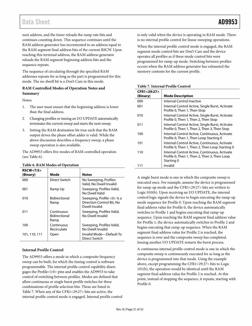
The AD9953 offers five modes of RAM controlled operation (see Table 6).
Table 6. RAM Modes of Operation RSCW<7:5> (Binary) Mode Notes 000 Direct Switch No Sweeping, Profiles
Valid, No Dwell Invalid 001 Ramp Up Sweeping, Profiles Valid,
No Dwell Valid 010 Bidirectional
Ramp Sweeping, Profile <0> Is a Direction Control Bit, No Dwell Invalid
011 Continuous Bidirectional Ramp
Sweeping, Profiles Valid, No Dwell Invalid
100 Continuous Recirculate
Sweeping, Profiles Valid, No Dwell Invalid
101, 110, 111 Open Invalid Mode—Default To Direct Switch
Internal Profile Control
The AD9953 offers a mode in which a composite frequency sweep can be built, for which the timing control is software programmable. The internal profile control capability disen-gages the Profile<1:0> pins and enables the AD9953 to take control of switching between profiles. Modes are defined that allow continuous or single burst profile switches for three combinations of profile selection bits. These are listed in Table 7. When any of the CFR1<29:27> bits are active, the internal profile control mode is engaged. Internal profile control
is only valid when the device is operating in RAM mode. There is no internal profile control for linear sweeping operations.
When the internal profile control mode is engaged, the RAM segment mode control bits are Don’t Care and the device operates all profiles as if these mode control bits were programmed for ramp-up mode. Switching between profiles occurs when the RAM address generator has exhausted the memory contents for the current profile.
Table 7. Internal Profile Control CFR1<29:27> (Binary) Mode Description 000 Internal Control Inactive 001 Internal Control Active, Single Burst, Activate
Profile 0, Then 1, Then Stop 010 Internal Control Active, Single Burst, Activate
Profile 0, Then 1, Then 2, Then Stop 011 Internal Control Active, Single Burst, Activate
Profile 0, Then 1, Then 2, Then 3, Then Stop 100 Internal Control Active, Continuous, Activate
Profile 0, Then 1, Then Loop Starting 0 101 Internal Control Active, Continuous, Activate
Profile 0, Then 1, Then 2, Then Loop Starting 0 110 Internal Control Active, Continuous, Activate
Profile 0, Then 1, Then 2, Then 3, Then Loop Starting 0
111 Invalid
A single burst mode is one in which the composite sweep is executed once. For example, assume the device is programmed for ramp-up mode and the CFR1<29:27> bits are written to Logic 010(b). Upon receiving an I/O UPDATE, the internal control logic signals the device to begin executing the ramp-up mode sequence for Profile 0. Upon reaching the RAM segment final address value for Profile 0, the device automatically switches to Profile 1 and begins executing that ramp-up sequence. Upon reaching the RAM segment final address value for Profile 1, the device automatically switches to Profile 2 and begins executing that ramp-up sequence. When the RAM segment final address value for Profile 2 is reached, the sequence is over and the composite sweep has completed. Issuing another I/O UPDATE restarts the burst process.
A continuous internal profile control mode is one in which the composite sweep is continuously executed for as long as the device is programmed into that mode. Using the example above, except programming the CFR1<29:27> bits to Logic 101(b), the operation would be identical until the RAM segment final address value for Profile 2 is reached. At this point, instead of stopping the sequence, it repeats, starting with Profile 0.
AD9953 Data Sheet
Rev. B | Page 22 of 32
PROGRAMMING AD9953 FEATURES Phase Offset Control
A 14-bit phase offset (θ) may be added to the output of the phase accumulator by means of the control registers. This feature provides the user with two different methods of phase control.
The first method is a static phase adjustment where a fixed phase offset is loaded into the appropriate phase offset register and left unchanged. The result is that the output signal is offset by a constant angle relative to the nominal signal. This allows the user to phase align the DDS output with some external signal, if necessary.
The second method of phase control is where the user regularly updates the phase offset register via the I/O port. By properly modifying the phase offset as a function of time, the user can implement a phase modulated output signal. However, both the speed of the I/O port and the frequency of SYSCLK limit the rate at which phase modulation can be performed.
The AD9953 allows for a programmable continuous zeroing of the phase accumulator as well as a clear and release or automatic zeroing function. Each feature is individually controlled via the CFR1 bits. CFR1<13> is the automatic clear phase accumulator bit. CFR1<10> clears the phase accumulator and holds the value to zero.
Continuous Clear Bit
The continuous clear bit is simply a static control signal that, when active high, holds the phase accumulator at zero for the entire time the bit is active. When the bit goes low, inactive, the phase accumulator is allowed to operate.
Clear and Release Function
When set, the auto-clear phase accumulator clears and releases the phase accumulator upon receiving an I/O UPDATE. The automatic clearing function is repeated for every subsequent I/O UPDATE until the appropriate auto-clear control bit is cleared.
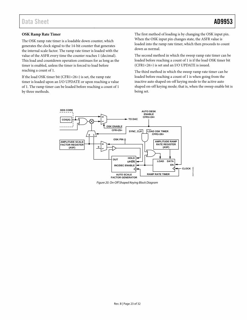
Shaped On-Off Keying
The shaped on-off keying function of the AD9953 allows the user to control the ramp-up and ramp-down time of an on-off emission from the DAC. This function is used in burst transmissions of digital data to reduce the adverse spectral impact of short, abrupt bursts of data.
Auto and manual shaped on-off keying modes are supported. The auto mode generates a linear scale factor at a rate determined by the amplitude ramp rate (ARR) register controlled by an external pin (OSK). Manual mode allows the user to directly control the output amplitude by writing the scale factor value into the amplitude scale factor (ASF) register.
The shaped on-off keying function may be bypassed (disabled) by clearing the OSK enable bit (CFR1<25> = 0).
The modes are controlled by two bits located in the most signifi-cant byte of the control function register (CFR). CFR1<25> is the shaped on-off keying enable bit. When CFR1<25> is set, the output scaling function is enabled and CFR1<25> bypasses the function. CFR1<24> is the internal shaped on-off keying active bit. When CFR1<24> is set, internal shaped on-off keying mode is active; CFR1<24> is cleared, external shaped on-off keying mode is active. CFR1<24> is a Don’t Care if the shaped on-off keying enable bit (CFR1<25>) is cleared. The power-up condition is shaped on-off keying disabled (CFR1<25> = 0). Figure 20 shows the block diagram of the OSK circuitry.
AUTO Shaped On-Off Keying Mode Operation
The auto shaped on-off keying mode is active when CFR1<25> and CFR1<24> are set. When auto shaped on-off keying mode is enabled, a single scale factor is internally generated and applied to the multiplier input for scaling the output of the DDS core block (see Figure 20). The scale factor is the output of a 14-bit counter that increments/decrements at a rate determined by the contents of the 8-bit output ramp rate register. The scale factor increases if the OSK pin is high and decreases if the OSK pin is low. The scale factor is an unsigned value such that all 0s multiply the DDS core output by 0 (decimal) and 0x3FFF multiplies the DDS core output by 16383 (decimal).
For those users who use the full amplitude (14 bits) but need fast ramp rates, the internally generated scale factor step size is controlled via the ASF<15:14> bits. Table 8 describes the increment/decrement step size of the internally generated scale factor per the ASF<15:14> bits.
A special feature of this mode is that the maximum output amplitude allowed is limited by the contents of the amplitude scale factor register. This allows the user to ramp to a value less than full scale.
Table 8. Auto-Scale Factor Internal Step Size ASF<15:14> (Binary) Increment/Decrement Size 00 1 01 2 10 4 11 8
Data Sheet AD9953
Rev. B | Page 23 of 32
OSK Ramp Rate Timer
The OSK ramp rate timer is a loadable down counter, which generates the clock signal to the 14-bit counter that generates the internal scale factor. The ramp rate timer is loaded with the value of the ASFR every time the counter reaches 1 (decimal). This load and countdown operation continues for as long as the timer is enabled, unless the timer is forced to load before reaching a count of 1.
If the load OSK timer bit (CFR1<26>) is set, the ramp rate timer is loaded upon an I/O UPDATE or upon reaching a value of 1. The ramp timer can be loaded before reaching a count of 1 by three methods.
The first method of loading is by changing the OSK input pin. When the OSK input pin changes state, the ASFR value is loaded into the ramp rate timer, which then proceeds to count down as normal.
The second method in which the sweep ramp rate timer can be loaded before reaching a count of 1 is if the load OSK timer bit (CFR1<26>) is set and an I/O UPDATE is issued.
The third method in which the sweep ramp rate timer can be loaded before reaching a count of 1 is when going from the inactive auto shaped on-off keying mode to the active auto shaped on-off keying mode; that is, when the sweep enable bit is being set.
0337
4-0-
005
OSK PIN
LOAD OSK TIMERCFR1<26>
SYNC_CLK
AUTO DESKENABLE
CFR1<24>TO DAC
AUTO SCALEFACTOR GENERATOR
RAMP RATE TIMER
CLOCK
DDS CORE
OSK ENABLECFR<25>
AMPLITUDE SCALEFACTOR REGISTER
(ASF)0
01
01
0 1
HOLD
INC/DEC ENABLE
OUT
COS(X)
AMPLITUDE RAMPRATE REGISTER
(ASF)
UP/DN DATALOADEN
Figure 20. On-Off Shaped Keying Block Diagram
AD9953 Data Sheet
Rev. B | Page 24 of 32
External Shaped On-Off Keying Mode Operation
The external shaped on-off keying mode is enabled by writing CFR1<25> to a Logic 1 and writing CFR1<24> to a Logic 0. When configured for external shaped on-off keying, the content of the ASFR becomes the scale factor for the data path. The scale factors are synchronized to SYNC_CLK via the I/O UPDATE functionality.
Synchronization; Register Updates (I/O UPDATE)
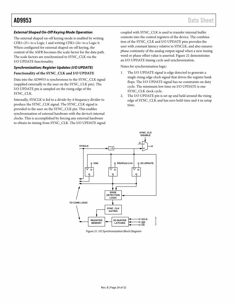
Functionality of the SYNC_CLK and I/O UPDATE
Data into the AD9953 is synchronous to the SYNC_CLK signal (supplied externally to the user on the SYNC_CLK pin). The I/O UPDATE pin is sampled on the rising edge of the SYNC_CLK.
Internally, SYSCLK is fed to a divide-by-4 frequency divider to produce the SYNC_CLK signal. The SYNC_CLK signal is provided to the user on the SYNC_CLK pin. This enables synchronization of external hardware with the device’s internal clocks. This is accomplished by forcing any external hardware to obtain its timing from SYNC_CLK. The I/O UPDATE signal
coupled with SYNC_CLK is used to transfer internal buffer contents into the control registers of the device. The combina-tion of the SYNC_CLK and I/O UPDATE pins provides the user with constant latency relative to SYSCLK, and also ensures phase continuity of the analog output signal when a new tuning word or phase offset value is asserted. Figure 21 demonstrates an I/O UPDATE timing cycle and synchronization.
Notes for synchronization logic:
1. The I/O UPDATE signal is edge detected to generate a single rising edge clock signal that drives the register bank flops. The I/O UPDATE signal has no constraints on duty cycle. The minimum low time on I/O UPDATE is one SYNC_CLK clock cycle.
2. The I/O UPDATE pin is set up and held around the rising edge of SYNC_CLK and has zero hold time and 4 ns setup time.
0337
4-0-
006
SYSCLK
SDI
SYNC_CLKDISABLE
10
0
SCLK
TO CORE LOGIC
CS
OSK
D
Q
PROFILE<1:0>
D
Q
I/O UPDATE
D
Q
÷ 4
SYNC_CLKGATING
EDGEDETECTION
LOGIC
REGISTERMEMORY
I/O BUFFERLATCHES
Figure 21. I/O Synchronization Block Diagram
Data Sheet AD9953
Rev. B | Page 25 of 32
SYSCLK
SYNC_CLK
I/O UPDATE
DATA INI/O BUFFERS
DATA INREGISTERS
A B A B
DATA 1 DATA 2 DATA 3
DATA 0 DATA 1 DATA 2
THE DEVICE REGISTERS AN I/O UPDATE AT POINT A. THE DATA IS TRANSFERRED FROM THE I/O BUFFERS AT POINT B. 0335
7-00
7
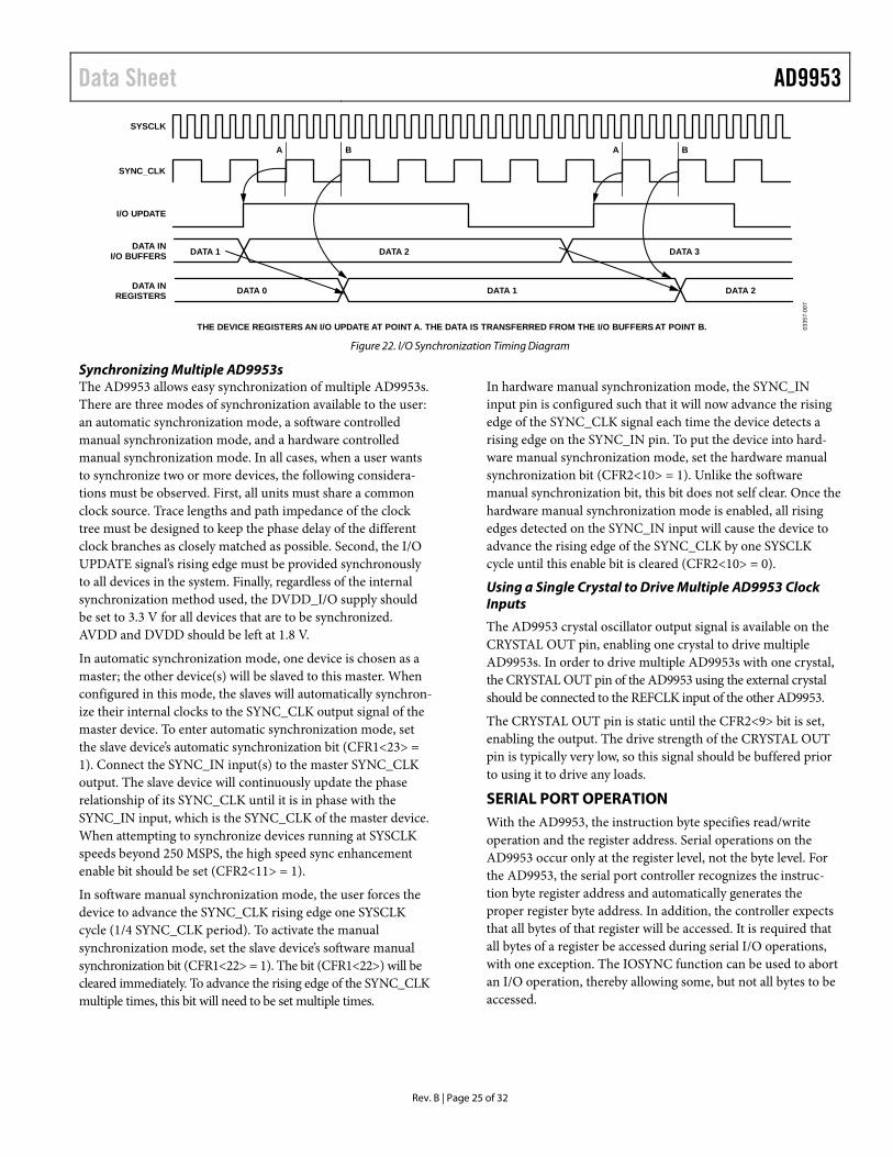
Figure 22. I/O Synchronization Timing Diagram
Synchronizing Multiple AD9953s The AD9953 allows easy synchronization of multiple AD9953s. There are three modes of synchronization available to the user: an automatic synchronization mode, a software controlled manual synchronization mode, and a hardware controlled manual synchronization mode. In all cases, when a user wants to synchronize two or more devices, the following considera-tions must be observed. First, all units must share a common clock source. Trace lengths and path impedance of the clock tree must be designed to keep the phase delay of the different clock branches as closely matched as possible. Second, the I/O UPDATE signal’s rising edge must be provided synchronously to all devices in the system. Finally, regardless of the internal synchronization method used, the DVDD_I/O supply should be set to 3.3 V for all devices that are to be synchronized. AVDD and DVDD should be left at 1.8 V.
In automatic synchronization mode, one device is chosen as a master; the other device(s) will be slaved to this master. When configured in this mode, the slaves will automatically synchron-ize their internal clocks to the SYNC_CLK output signal of the master device. To enter automatic synchronization mode, set the slave device’s automatic synchronization bit (CFR1<23> = 1). Connect the SYNC_IN input(s) to the master SYNC_CLK output. The slave device will continuously update the phase relationship of its SYNC_CLK until it is in phase with the SYNC_IN input, which is the SYNC_CLK of the master device. When attempting to synchronize devices running at SYSCLK speeds beyond 250 MSPS, the high speed sync enhancement enable bit should be set (CFR2<11> = 1).
In software manual synchronization mode, the user forces the device to advance the SYNC_CLK rising edge one SYSCLK cycle (1/4 SYNC_CLK period). To activate the manual synchronization mode, set the slave device’s software manual synchronization bit (CFR1<22> = 1). The bit (CFR1<22>) will be cleared immediately. To advance the rising edge of the SYNC_CLK multiple times, this bit will need to be set multiple times.
In hardware manual synchronization mode, the SYNC_IN input pin is configured such that it will now advance the rising edge of the SYNC_CLK signal each time the device detects a rising edge on the SYNC_IN pin. To put the device into hard-ware manual synchronization mode, set the hardware manual synchronization bit (CFR2<10> = 1). Unlike the software manual synchronization bit, this bit does not self clear. Once the hardware manual synchronization mode is enabled, all rising edges detected on the SYNC_IN input will cause the device to advance the rising edge of the SYNC_CLK by one SYSCLK cycle until this enable bit is cleared (CFR2<10> = 0).
Using a Single Crystal to Drive Multiple AD9953 Clock Inputs
The AD9953 crystal oscillator output signal is available on the CRYSTAL OUT pin, enabling one crystal to drive multiple AD9953s. In order to drive multiple AD9953s with one crystal, the CRYSTAL OUT pin of the AD9953 using the external crystal should be connected to the REFCLK input of the other AD9953.
The CRYSTAL OUT pin is static until the CFR2<9> bit is set, enabling the output. The drive strength of the CRYSTAL OUT pin is typically very low, so this signal should be buffered prior to using it to drive any loads.
SERIAL PORT OPERATION With the AD9953, the instruction byte specifies read/write operation and the register address. Serial operations on the AD9953 occur only at the register level, not the byte level. For the AD9953, the serial port controller recognizes the instruc-tion byte register address and automatically generates the proper register byte address. In addition, the controller expects that all bytes of that register will be accessed. It is required that all bytes of a register be accessed during serial I/O operations, with one exception. The IOSYNC function can be used to abort an I/O operation, thereby allowing some, but not all bytes to be accessed.
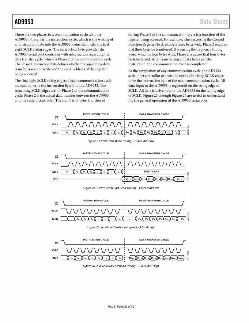
AD9953 Data Sheet
Rev. B | Page 26 of 32
There are two phases to a communication cycle with the AD9953. Phase 1 is the instruction cycle, which is the writing of an instruction byte into the AD9953, coincident with the first eight SCLK rising edges. The instruction byte provides the AD9953 serial port controller with information regarding the data transfer cycle, which is Phase 2 of the communication cycle. The Phase 1 instruction byte defines whether the upcoming data transfer is read or write and the serial address of the register being accessed.
The first eight SCLK rising edges of each communication cycle are used to write the instruction byte into the AD9953. The remaining SCLK edges are for Phase 2 of the communication cycle. Phase 2 is the actual data transfer between the AD9953 and the system controller. The number of bytes transferred
during Phase 2 of the communication cycle is a function of the register being accessed. For example, when accessing the Control Function Register No. 2, which is three bytes wide, Phase 2 requires that three bytes be transferred. If accessing the frequency tuning word, which is four bytes wide, Phase 2 requires that four bytes be transferred. After transferring all data bytes per the instruction, the communication cycle is completed.
At the completion of any communication cycle, the AD9953 serial port controller expects the next eight rising SCLK edges to be the instruction byte of the next communication cycle. All data input to the AD9953 is registered on the rising edge of SCLK. All data is driven out of the AD9953 on the falling edge of SCLK. Figure 23 through Figure 26 are useful in understand-ing the general operation of the AD9953 serial port.
0337
4-0-
008
I6 I5 I4 I3 I2 I1 D5 D4 D3 D2 D1 D0I0 D7 D6I7
INSTRUCTION CYCLE
SCLK
SDIO
DATA TRANSFER CYCLECS
Figure 23. Serial Port Write Timing—Clock Stall Low
0337
4-0-
009I6 I5 I4 I3 I2 I1 I0 DON'T CAREI7
INSTRUCTION CYCLE
SCLK
SDIO
DATA TRANSFER CYCLE
DO 5 DO 4 DO 3 DO 2 DO 1 DO 0DO 7 DO 6SDO
CS
Figure 24. 3-Wire Serial Port Read Timing—Clock Stall Low
0337
4-0-
010
I6 I5 I4 I3 I2 I1 D5 D4 D3 D2 D1 D0I0 D7 D6I7
INSTRUCTION CYCLE
SCLK
SDIO
DATA TRANSFER CYCLECS
Figure 25. Serial Port Write Timing—Clock Stall High
0337
4-0-
011
I6 I5 I4 I3 I2 I1 DO 5 DO 4 DO 3 DO 2 DO 1 DO 0I0 DO 7 DO 6I7
INSTRUCTION CYCLE
SCLK
SDIO
DATA TRANSFER CYCLECS
Figure 26. 2-Wire Serial Port Read Timing—Clock Stall High
Data Sheet AD9953
Rev. B | Page 27 of 32
INSTRUCTION BYTE The instruction byte contains the following information:
Table 9. MSB D6 D5 D4 D3 D2 D1 LSB
R/W X X A4 A3 A2 A1 A0
R/W—Bit 7 of the instruction byte determines whether a read or write data transfer will occur after the instruction byte write. Logic High indicates read operation. Logic 0 indicates a write operation.
X, X—Bits 6 and 5 of the instruction byte are Don’t Care.
A4, A3, A2, A1, A0—Bits 4, 3, 2, 1, 0 of the instruction byte determine which register is accessed during the data transfer portion of the communications cycle.
SERIAL INTERFACE PORT PIN DESCRIPTION SCLK—Serial Clock. The serial clock pin is used to synchronize data to and from the AD9953 and to run the internal state machines. SCLK maximum frequency is 25 MHz.
CSB—Chip Select Bar. CSB is active low input that allows more than one device on the same serial communications line. The SDO and SDIO pins will go to a high impedance state when this input is high. If driven high during any communications cycle, that cycle is suspended until CS is reactivated low. Chip select can be tied low in systems that maintain control of SCLK.
SDIO—Serial Data I/O. Data is always written into the AD9953 on this pin. However, this pin can be used as a bidirectional data line. Bit 9 of Register Address 0x00 controls the configuration of this pin. The default is Logic 0, which configures the SDIO pin as bidirectional.
SDO—Serial Data Out. Data is read from this pin for protocols that use separate lines for transmitting and receiving data. In the case where the AD9953 operates in a single bidirectional I/O mode, this pin does not output data and is set to a high impedance state.
IOSYNC—It synchronizes the I/O port state machines without affecting the addressable register’s contents. An active high input on the IOSYNC pin causes the current communication cycle to abort. After IOSYNC returns low (Logic 0), another communication cycle may begin, starting with the instruction byte write.
MSB/LSB TRANSFERS The AD9953 serial port can support both most significant bit (MSB) first or least significant bit (LSB) first data formats. This functionality is controlled by the Control Register 0x00 <8> bit. The default value of Control Register 0x00 <8> is low (MSB first). When Control Register 0x00 <8> is set high, the AD9953 serial port is in LSB first format. The instruction byte must be
written in the format indicated by Control Register 0x00 <8>. If the AD9953 is in LSB first mode, the instruction byte must be written from least significant bit to most significant bit.
For MSB first operation, the serial port controller will generate the most significant byte (of the specified register) address first followed by the next lesser significant byte addresses until the I/O operation is complete. All data written to (read from) the AD9953 must be (will be) in MSB first order. If the LSB mode is active, the serial port controller will generate the least signifi-cant byte address first followed by the next greater significant byte addresses until the I/O operation is complete. All data written to (read from) the AD9953 must be (will be) in LSB first order.
Example Operation
To write the amplitude scale factor register in MSB first format, apply an instruction byte of 0x02 [serial address is 00010(b)]. From this instruction, the internal controller will know to use the first byte as the most significant byte. The first two bits will be recorded as the auto ramp rate speed control bits, and the next six bits will be the most significant bits of the amplitude scale factor. The second byte will be applied as the eight less significant bits of the amplitude scale factor ASF<7:0>.
To write the amplitude scale factor register in LSB first format, assuming the control register has already been set for LSB first format, apply an instruction byte of 0x40. From this instruction, the internal controller will know to use the first byte as the least significant byte of the amplitude scale factor ASF<0:7>. The second byte will be split into the first six bits ASF<8:13> and the last two will provide the auto ramp rate speed control bits ARRSC<0:1>.
Power-Down Functions of the AD9953
The AD9953 supports an externally controlled or hardware power-down feature as well as the more common software programmable power-down bits found in previous ADI DDS products.
The software control power-down allows the DAC, PLL, input clock circuitry, and digital logic to be individually powered down via unique control bits (CFR1<7:4>). With the exception of CFR1<6>, these bits are not active when the externally controlled power-down pin (PWRDWNCTL) is high. External power-down control is supported on the AD9953 via the PWRDWNCTL input pin. When the PWRDWNCTL input pin is high, the AD9953 will enter a power-down mode based on the CFR1<3> bit. When the PWRDWNCTL input pin is low, the external power-down control is inactive.
AD9953 Data Sheet
Rev. B | Page 28 of 32
When the CFR1<3> bit is 0 and the PWRDWNCTL input pin is high, the AD9953 is put into a fast recovery power-down mode. In this mode, the digital logic and the DAC digital logic are powered down. The DAC bias circuitry, PLL, oscillator, and clock input circuitry is not powered down.
When the CFR1<3> bit is high, and the PWRDWNCTL input pin is high, the AD9953 is put into the full power-down mode. In this mode, all functions are powered down. This includes the DAC and PLL, which take a significant amount of time to power up.
When the PWRDWNCTL input pin is high, the individual power-down bits (CFR1<7>, <5:4>) are invalid (Don’t Care) and unused. When the PWRDWNCTL input pin is low, the individual power-down bits control the power-down modes of operation.
Note that the power-down signals are all designed such that a Logic 1 indicates the low power mode and a Logic 0 indicates the active or power-up mode.
Table 10 indicates the logic level for each power-down bit that drives out of the AD9953 core logic to the analog section and
the digital clock generation section of the chip for the external power-down operation.
Layout Considerations
For the best performance, the following layout guidelines should be observed. Always provide the analog power supply (AVDD) and the digital power supply (DVDD) on separate supplies, even if just from two different voltage regulators driven by a common supply. Likewise, the ground connections (AGND, DGND) should be kept separate as far back to the source as possible (i.e., separate the ground planes on a localized board even if the grounds connect to a common point in the system). Bypass capacitors should be placed as close to the device pin as possible. Usually a multitiered bypassing scheme consisting of a small high frequency capacitor (100 pF) placed close to the supply pin and progressively larger capaci-tors (0.1 µF, 10 µF) placed further away from the actual supply source works best.
Table 10. Power-Down Control Functions Control Mode Active Description PWRDWNCTL = 0 CFR1<3> Don’t Care Software Control Digital Power-Down = CFR1<7>
DAC Power-Down = CFR1<5> Input Clock Power-Down = CFR1<4>
PWRDWNCTL = 1 CFR1<3> = 0 External Control, Fast Recovery Power-Down Mode
Digital Power-Down = 1’b1 DAC Power-Down = 1’b0 Input Clock Power-Down = 1’b0
PWRDWNCTL = 1 CFR1<3> = 1 External Control, Full Power-Down Mode
Digital Power-Down = 1’b1 DAC Power-Down = 1’b1 Input Clock Power-Down = 1’b1
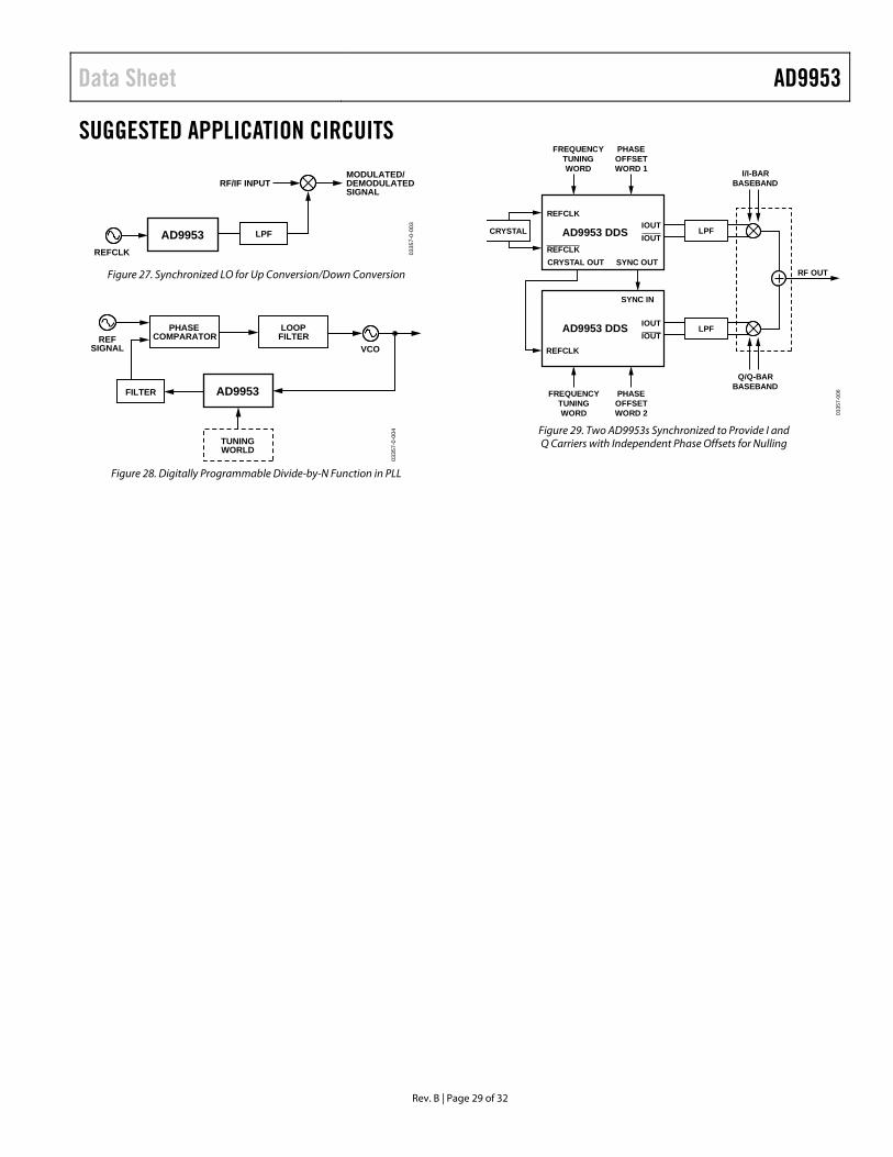
Data Sheet AD9953
Rev. B | Page 29 of 32
SUGGESTED APPLICATION CIRCUITS
0335
7-0-
003
LPFAD9953REFCLK
RF/IF INPUTMODULATED/DEMODULATEDSIGNAL
Figure 27. Synchronized LO for Up Conversion/Down Conversion
0335
7-0-
004
FILTER
PHASECOMPARATOR
LOOPFILTER
AD9953
TUNINGWORLD
REFSIGNAL VCO
Figure 28. Digitally Programmable Divide-by-N Function in PLL
0335
7-00
6
CRYSTAL
FREQUENCYTUNINGWORD
PHASEOFFSETWORD 2
I/I-BARBASEBAND
FREQUENCYTUNINGWORD
PHASEOFFSETWORD 1
Q/Q-BARBASEBAND
SYNC IN
AD9953 DDS
REFCLK
REFCLK
REFCLK
LPF
SYNC OUTCRYSTAL OUT
AD9953 DDS IOUTIOUT
LPFIOUTIOUT
RF OUT
Figure 29. Two AD9953s Synchronized to Provide I and Q Carriers with Independent Phase Offsets for Nulling
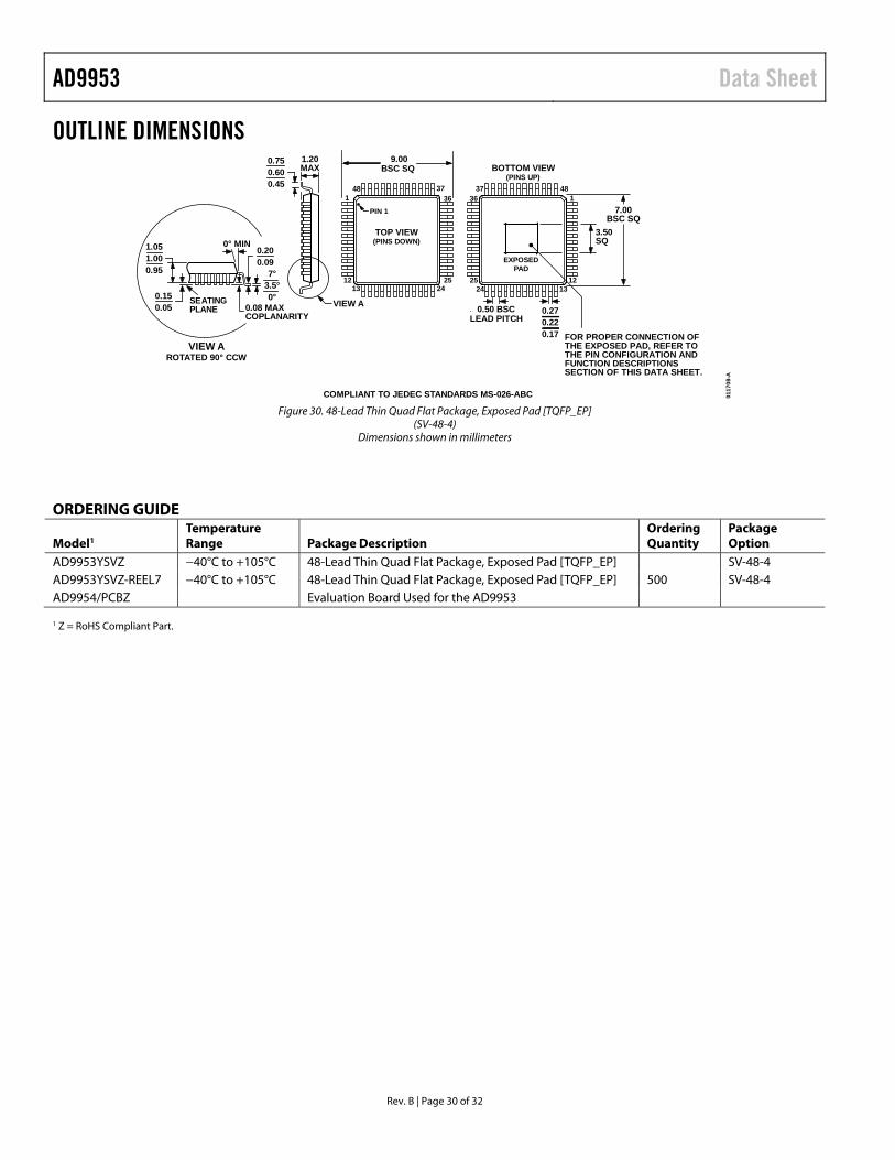
AD9953 Data Sheet
Rev. B | Page 30 of 32
OUTLINE DIMENSIONS
FOR PROPER CONNECTION OFTHE EXPOSED PAD, REFER TOTHE PIN CONFIGURATION ANDFUNCTION DESCRIPTIONSSECTION OF THIS DATA SHEET.
COMPLIANT TO JEDEC STANDARDS MS-026-ABC
0.50 BSCLEAD PITCH
0.270.220.17
9.00BSC SQ
7.00BSC SQ
37 3748 481
1312
1
1224 1324
25
36
25
36
1.051.000.95
0.200.09
0.08 MAXCOPLANARITY
VIEW AROTATED 90° CCW
SEATINGPLANE
0° MIN
7°3.5°0°0.15
0.05
0.750.600.45
1.20MAX
VIEW A
TOP VIEW(PINS DOWN)
BOTTOM VIEW(PINS UP)
PIN 1
3.50SQ
EXPOSEDPAD
0117
08-A
Figure 30. 48-Lead Thin Quad Flat Package, Exposed Pad [TQFP_EP]
(SV-48-4) Dimensions shown in millimeters
ORDERING GUIDE
Model1 Temperature Range Package Description
Ordering Quantity
Package Option
AD9953YSVZ −40°C to +105°C 48-Lead Thin Quad Flat Package, Exposed Pad [TQFP_EP] SV-48-4 AD9953YSVZ-REEL7 −40°C to +105°C 48-Lead Thin Quad Flat Package, Exposed Pad [TQFP_EP] 500 SV-48-4 AD9954/PCBZ Evaluation Board Used for the AD9953 1 Z = RoHS Compliant Part.

Data Sheet AD9953
Rev. B | Page 31 of 32
NOTES

AD9953 Data Sheet
Rev. B | Page 32 of 32
NOTES
©2004–2017 Analog Devices, Inc. All rights reserved. Trademarks and registered trademarks are the property of their respective owners. D03374-0-1/17(B)
Related Documents