0 5 10 15 20 25 0 10 20 30 40 Input Voltage (V) C003 Quiescent Current (A) –40°C 25°C 125°C MSP430 TPS7A19 DELAY FB 4 V to 40 V OUT PG IO VDD IN GND EN VIN VOUT Copyright © 2016, Texas Instruments Incorporated Product Folder Sample & Buy Technical Documents Tools & Software Support & Community An IMPORTANT NOTICE at the end of this data sheet addresses availability, warranty, changes, use in safety-critical applications, intellectual property matters and other important disclaimers. PRODUCTION DATA. TPS7A19 SBVS256A – MAY 2016 – REVISED SEPTEMBER 2016 TPS7A19 40-V, 450-mA, Wide V IN , Low I Q , Low-Dropout Voltage Regulator with Power Good 1 1 Features 1• Wide Input Voltage Range: 4 V to 40 V • Adjustable Output Voltage: 1.5 V to 18 V • Output Current: 450 mA • Low Quiescent Current (I Q ): 15 μA • Low Dropout Voltage: 450 mV (max) at 400 mA • Power Good with Programmable Delay • Thermal Shutdown and Overcurrent Protection • Stable with Ceramic Output Capacitors: – 10 μF to 500 μF for V OUT ≥ 2.5 V – 22 μF to 500 μF for V OUT < 2.5 V • Operating Temperature: –40°C to +125°C • Package: 3-mm × 3-mm SON-8 2 Applications • Smart Grid Infrastructure and Metering • Power Tools • Motor Drives • Access Control Systems • Test and Measurement 3 Description The TPS7A19 is a low-dropout linear regulator (LDO) with a wide input voltage (V IN ) range up to 40 V, capable of sourcing high output current (I OUT ) up to 450 mA. This voltage regulator is ideal for generating a low-voltage supply from wide input-voltage rails. Not only does the TPS7A19 supply a well-regulated voltage rail, but the device also withstands and maintains regulation during voltage transients by acting as a simple surge protection circuit. The TPS7A19 consumes only 15 μA of quiescent current (I Q ) at light loads, thereby lowering the power consumption for always-on or battery-powered applications. The TPS7A19 features integrated thermal shutdown and overcurrent protection. The TPS7A19 also offers a power good output (PG) with a programmable delay that indicates when the output voltage is in regulation. This feature is useful for power-rail sequencing functions. This LDO is available in a small, 3-mm × 3-mm, thermally-enhanced, 8-pin SON package. Device Information (1) PART NUMBER PACKAGE BODY SIZE (NOM) TPS7A19 SON (8) 3.00 mm × 3.00 mm (1) For all available packages, see the package option addendum at the end of the data sheet. Typical Application Schematic Quiescent Current vs Input Voltage at V OUT = 1.5 V

Welcome message from author
This document is posted to help you gain knowledge. Please leave a comment to let me know what you think about it! Share it to your friends and learn new things together.
Transcript

0
5
10
15
20
25
0 10 20 30 40
Input Voltage (V) C003
Qui
esce
nt C
urre
nt (�
A)
±40°C
25°C
125°C
MSP430
TPS7A19
DELAYFB
4 V to 40 V
OUT
PG
IO
VDD
IN
GND
EN
VINVOUT
Copyright © 2016, Texas Instruments Incorporated
Product
Folder
Sample &Buy
Technical
Documents
Tools &
Software
Support &Community
An IMPORTANT NOTICE at the end of this data sheet addresses availability, warranty, changes, use in safety-critical applications,intellectual property matters and other important disclaimers. PRODUCTION DATA.
TPS7A19SBVS256A –MAY 2016–REVISED SEPTEMBER 2016
TPS7A1940-V, 450-mA, Wide VIN, Low IQ, Low-Dropout Voltage Regulator with Power Good
1
1 Features1• Wide Input Voltage Range: 4 V to 40 V• Adjustable Output Voltage: 1.5 V to 18 V• Output Current: 450 mA• Low Quiescent Current (IQ): 15 µA• Low Dropout Voltage: 450 mV (max) at 400 mA• Power Good with Programmable Delay• Thermal Shutdown and Overcurrent Protection• Stable with Ceramic Output Capacitors:
– 10 µF to 500 µF for VOUT ≥ 2.5 V– 22 µF to 500 µF for VOUT < 2.5 V
• Operating Temperature: –40°C to +125°C• Package: 3-mm × 3-mm SON-8
2 Applications• Smart Grid Infrastructure and Metering• Power Tools• Motor Drives• Access Control Systems• Test and Measurement
3 DescriptionThe TPS7A19 is a low-dropout linear regulator (LDO)with a wide input voltage (VIN) range up to 40 V,capable of sourcing high output current (IOUT) up to450 mA. This voltage regulator is ideal for generatinga low-voltage supply from wide input-voltage rails.Not only does the TPS7A19 supply a well-regulatedvoltage rail, but the device also withstands andmaintains regulation during voltage transients byacting as a simple surge protection circuit.
The TPS7A19 consumes only 15 µA of quiescentcurrent (IQ) at light loads, thereby lowering the powerconsumption for always-on or battery-poweredapplications.
The TPS7A19 features integrated thermal shutdownand overcurrent protection. The TPS7A19 also offersa power good output (PG) with a programmable delaythat indicates when the output voltage is in regulation.This feature is useful for power-rail sequencingfunctions.
This LDO is available in a small, 3-mm × 3-mm,thermally-enhanced, 8-pin SON package.
Device Information(1)
PART NUMBER PACKAGE BODY SIZE (NOM)TPS7A19 SON (8) 3.00 mm × 3.00 mm
(1) For all available packages, see the package option addendumat the end of the data sheet.
Typical Application Schematic Quiescent Current vs Input Voltageat VOUT = 1.5 V
2
TPS7A19SBVS256A –MAY 2016–REVISED SEPTEMBER 2016 www.ti.com
Product Folder Links: TPS7A19
Submit Documentation Feedback Copyright © 2016, Texas Instruments Incorporated
Table of Contents1 Features .................................................................. 12 Applications ........................................................... 13 Description ............................................................. 14 Revision History..................................................... 25 Pin Configuration and Functions ......................... 36 Specifications......................................................... 4
6.1 Absolute Maximum Ratings ...................................... 46.2 ESD Ratings.............................................................. 46.3 Recommended Operating Conditions....................... 46.4 Thermal Information .................................................. 46.5 Electrical Characteristics........................................... 56.6 Timing Requirements ................................................ 56.7 Typical Characteristics .............................................. 6
7 Detailed Description .............................................. 87.1 Overview ................................................................... 87.2 Functional Block Diagram ......................................... 87.3 Feature Description................................................... 8
7.4 Device Functional Modes........................................ 108 Application and Implementation ........................ 11
8.1 Application Information............................................ 118.2 Typical Application .................................................. 11
9 Power Supply Recommendations ...................... 1310 Layout................................................................... 13
10.1 Layout Guidelines ................................................. 1310.2 Layout Example .................................................... 13
11 Device and Documentation Support ................. 1411.1 Device Support...................................................... 1411.2 Documentation Support ....................................... 1411.3 Receiving Notification of Documentation Updates 1411.4 Community Resources.......................................... 1411.5 Trademarks ........................................................... 1411.6 Electrostatic Discharge Caution............................ 1511.7 Glossary ................................................................ 15
12 Mechanical, Packaging, and OrderableInformation ........................................................... 15
4 Revision History
Changes from Original (May 2016) to Revision A Page
• Changed from product preview to production data ................................................................................................................ 1
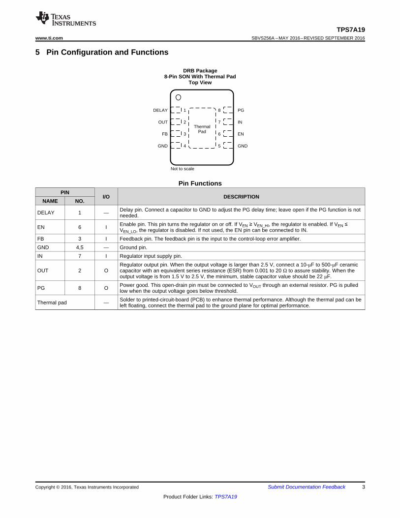
1DELAY 8 PG
2OUT 7 IN
3FB 6 EN
4GND 5 GND
Not to scale
ThermalPad
3
TPS7A19www.ti.com SBVS256A –MAY 2016–REVISED SEPTEMBER 2016
Product Folder Links: TPS7A19
Submit Documentation FeedbackCopyright © 2016, Texas Instruments Incorporated
5 Pin Configuration and Functions
DRB Package8-Pin SON With Thermal Pad
Top View
Pin FunctionsPIN
I/O DESCRIPTIONNAME NO.
DELAY 1 — Delay pin. Connect a capacitor to GND to adjust the PG delay time; leave open if the PG function is notneeded.
EN 6 I Enable pin. This pin turns the regulator on or off. If VEN ≥ VEN_HI, the regulator is enabled. If VEN ≤VEN_LO, the regulator is disabled. If not used, the EN pin can be connected to IN.
FB 3 I Feedback pin. The feedback pin is the input to the control-loop error amplifier.GND 4,5 — Ground pin.IN 7 I Regulator input supply pin.
OUT 2 ORegulator output pin. When the output voltage is larger than 2.5 V, connect a 10-μF to 500-μF ceramiccapacitor with an equivalent series resistance (ESR) from 0.001 to 20 Ω to assure stability. When theoutput voltage is from 1.5 V to 2.5 V, the minimum, stable capacitor value should be 22 μF.
PG 8 O Power good. This open-drain pin must be connected to VOUT through an external resistor. PG is pulledlow when the output voltage goes below threshold.
Thermal pad — Solder to printed-circuit-board (PCB) to enhance thermal performance. Although the thermal pad can beleft floating, connect the thermal pad to the ground plane for optimal performance.

4
TPS7A19SBVS256A –MAY 2016–REVISED SEPTEMBER 2016 www.ti.com
Product Folder Links: TPS7A19
Submit Documentation Feedback Copyright © 2016, Texas Instruments Incorporated
(1) Stresses beyond those listed under absolute maximum ratings may cause permanent damage to the device. These are stress ratingsonly and functional operation of the device at these or any other conditions beyond those indicated under recommended operatingconditions is not implied. Exposure to absolute-maximum-rated conditions for extended periods may affect device reliability.
(2) All voltage values are with respect to GND.(3) The absolute maximum rating is VIN + 0.3 V or 22 V, whichever is lower.(4) The voltage at the DELAY pin must be lower than the VIN voltage.
6 Specifications
6.1 Absolute Maximum Ratingsover operating free-air temperature range –40°C to 125°C(unless otherwise noted) (1)
MIN MAX UNIT
Voltage (2)
Input IN, EN –0.3 45
VOutput
OUT (3) –0.3 VIN + 0.3DELAY (4) –0.3 45FB, PG –0.3 22
Current Peak output Internally limited
TemperatureOperating junction, TJ –40 150
°CStorage, Tstg –65 150
(1) JEDEC document JEP155 states that 500-V HBM allows safe manufacturing with a standard ESD control process.(2) JEDEC document JEP157 states that 250-V CDM allows safe manufacturing with a standard ESD control process.
6.2 ESD RatingsVALUE UNIT
V(ESD) Electrostatic dischargeHuman-body model (HBM), per ANSI/ESDA/JEDEC JS-001 (1) ±2000
VCharged-device model (CDM), per JEDEC specification JESD22-C101 (2) ±500
6.3 Recommended Operating Conditionsover operating free-air temperature range (unless otherwise noted)
MIN MAX UNITVIN Input supply voltage 4 40 VVOUT Output voltage 1.5 18 VVEN Enable voltage 0 40 VTJ Operating junction temperature –40 125 °C
(1) For information about traditional and new thermal metrics, see the Semiconductor and IC Package Thermal Metrics application report.
6.4 Thermal Information
THERMAL METRIC (1)TPS7A19
UNITDRB (VSON)8 PINS
RθJA Junction-to-ambient thermal resistance 48 °C/WRθJC(top) Junction-to-case (top) thermal resistance 56.3 °C/WRθJB Junction-to-board thermal resistance 22.4 °C/WψJT Junction-to-top characterization parameter 0.9 °C/WψJB Junction-to-board characterization parameter 22.5 °C/WRθJC(bot) Junction-to-case (bottom) thermal resistance 4.6 °C/W

5
TPS7A19www.ti.com SBVS256A –MAY 2016–REVISED SEPTEMBER 2016
Product Folder Links: TPS7A19
Submit Documentation FeedbackCopyright © 2016, Texas Instruments Incorporated
(1) Accuracy specification does not apply on any application condition that exceeds the power dissipation limit of the package under test.External resistor divider variation is not considered for accuracy measurement.
(2) Design information; not tested, specified by characterization.
6.5 Electrical Characteristicsat TJ = –40°C to +125°C, VIN = 14 V , VEN = VIN, IOUT = 200 μA, CIN = 22 μF, and COUT = 47 μF (unless otherwise noted)
PARAMETER TEST CONDITIONS MIN TYP MAX UNIT
SUPPLY VOLTAGE AND CURRENT
VIN Input voltageVOUT ≤ 3.5 V , IOUT = 0 mA to 450 mA 4 40 V
VOUT ≥ 3.5 V , IOUT = 0 mA to 450 mA VOUT + 0.5 40 V
IQ Quiescent currentVIN = 4 V to 40 V, VOUT = 1.5 V, VEN = 5 V, IOUT = 0.2 mA 15 25
µAVIN = 18.5 V to 40 V, VOUT = 18 V, VEN = 5 V, IOUT = 0.2 mA 25 40
ISHDN Shutdown current VEN = 0 V, IOUT = 0 mA , VIN = 18 V, VOUT = 1.5 V 4 µA
VFB Feedback voltage Reference voltage for FB pin 1.208 1.233 1.258 V
VIN_UVLO Undervoltage lockout Ramp VIN down until output is turned off 2.6 V
UVLOHysUndervoltage detectionhysteresis VIN rising 1 V
ENABLE INPUT (EN)
VEN_LO Logic input low level 0 0.4 V
VEN_HI Logic input high level 1.7 V
IEN EN pin current VEN = 40 V , VIN = 14 V 1 µA
REGULATED OUTPUT
VOUT Regulated output (1) VIN = VOUT + 1 V to 40 V and VIN ≥ 4 V,IOUT = 100 µA to 450 mA –2% 2%
ΔVO(ΔVI) Line regulation VIN = VOUT + 1 V to 40 V and VIN ≥ 4 V, IOUT = 100 mA 10 mV
ΔVO(ΔIL) Load regulation IOUT = 1 mA to 450 mA, VIN = VOUT + 1 V and VIN ≥ 4 V 10 mV
VDO Dropout voltageVIN – VOUT, IOUT = 400 mA 240 450
mVVIN – VOUT, IOUT = 200 mA 160 300
IOUT Output current VOUT in regulation 0 450 mA
ICL Output current-limitVOUT short to ground 140 360
mAVOUT = VOUT nominal × 0.9 470 850
PSRR Power-supply ripple rejection (2) IOUT = 100 mA, COUT = 22 µFf = 100 Hz 60
dBf = 100 kHz 40
PG
VOL PG output low voltage IOL = 0.5 mA 0.4 V
IOH PG leakage current PG pulled to VOUTwith 10-kΩ resistor 1 µA
VT(PG) Power good threshold VOUT power-up 89.6 91.6 93.6 % of VOUT
Vhys Hysteresis VOUT power-down 2 % of VOUT
PG DELAY
IDelay Delay capacitor charging current 5 9.5 14 µA
VT(PG_DLY)Delay pin comparator thresholdvoltage 1 V
TEMPERATURE
Tsd Junction shutdown temperature Temperature increasing 175 °C
Thys Hysteresis of thermal shutdown 24 °C
(1) Information only; not tested in production. The equation is based on: (C × 1) / (9.5 × 10⁻⁶) = tPG_DLY, where C = delay capacitor valuecapacitance; range = 100 pF to 500 nF.
6.6 Timing RequirementsMIN TYP MAX UNIT
TIMING FOR PGtPG_DLY Power good delay C = delay-capacitor value capacitance = 100 nF (1) 10.5 mstPG-fixed Power good delay No capacitor on pin 325 µstPG(HL) PG falling propagation delay VOUT low to PG low 180 µs
0
5
10
15
20
25
30
35
15 20 25 30 35 40 45
C005 Input Voltage (V)
Qui
esce
nt C
urre
nt (�
A)
±40°C
25°C
125°C0
50
100
150
200
250
300
350
400
0 50 100 150 200 250 300 350 400 450
Dro
pout
Vol
tage
(m
V)
Output Current (mA)
±40°C
25°C
125°C
0
20
40
60
80
100
120
140
160
0 50 100 150 200 250 300 350 400 450
C004
Gro
und
Cur
rent
(�
A)
Output Current (mA)
±40°C
25°C
125°C0
5
10
15
20
25
0 10 20 30 40
Input Voltage (V) C003
Qui
esce
nt C
urre
nt (�
A)
±40°C
25°C
125°C
0
20
40
60
80
100
120
140
160
0 50 100 150 200 250 300 350 400 450
Output Current (mA) C0
02
Gro
und
Cur
rent
(�
A)
±40°C
25°C
125°C1.40
1.42
1.44
1.46
1.48
1.50
1.52
1.54
1.56
1.58
1.60
0 5 10 15 20 25 30 35 40
Input Voltage (V)
Out
put V
olta
ge, N
omin
al (
V)
±40°C
25°C
125°C
6
TPS7A19SBVS256A –MAY 2016–REVISED SEPTEMBER 2016 www.ti.com
Product Folder Links: TPS7A19
Submit Documentation Feedback Copyright © 2016, Texas Instruments Incorporated
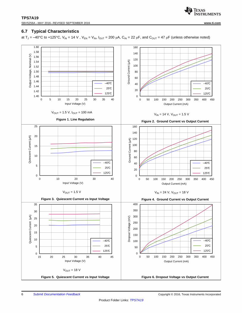
6.7 Typical Characteristicsat TJ = –40°C to +125°C, VIN = 14 V , VEN = VIN, IOUT = 200 μA, CIN = 22 μF, and COUT = 47 μF (unless otherwise noted)
VOUT = 1.5 V, IOUT = 100 mA
Figure 1. Line RegulationVIN = 14 V, VOUT = 1.5 V
Figure 2. Ground Current vs Output Current
VOUT = 1.5 V
Figure 3. Quiescent Current vs Input Voltage
VIN = 24 V, VOUT = 18 V
Figure 4. Ground Current vs Output Current
VOUT = 18 V
Figure 5. Quiescent Current vs Input Voltage Figure 6. Dropout Voltage vs Output Current

190
195
200
205
210
215
220
±40 ±25 ±10 5 20 35 50 65 80 95 110 125
Cur
rent
Lim
it (m
A)
Temperature (�C) C013
520
530
540
550
560
570
580
590
600
610
620
630
±40 ±25 ±10 5 20 35 50 65 80 95 110 125
Cur
rent
Lim
it (m
A)
Temperature (�C) C014
0
20
40
60
80
100
120
10 100 1000 10000 100000 1000000 10000000 100000000
Frequency (Hz)
10 100 1k 10k 100k 1M 10M
Pow
er S
uppl
y R
ejec
tion
Rat
io (
dB)
1.40
1.42
1.44
1.46
1.48
1.50
1.52
1.54
1.56
1.58
1.60
0 50 100 150 200 250 300 350 400 450
C007
Output Current (mA)
Out
put V
olta
ge (
V)
±40°C
25°C
125°C
7
TPS7A19www.ti.com SBVS256A –MAY 2016–REVISED SEPTEMBER 2016
Product Folder Links: TPS7A19
Submit Documentation FeedbackCopyright © 2016, Texas Instruments Incorporated
Typical Characteristics (continued)at TJ = –40°C to +125°C, VIN = 14 V , VEN = VIN, IOUT = 200 μA, CIN = 22 μF, and COUT = 47 μF (unless otherwise noted)
VIN = 14 V, VOUT = 1.5 V
Figure 7. Load Regulation
VOUT = 5 V, COUT = 47 µF, IOUT = 10 mA
Figure 8. Power-Supply Rejection Ratio vs Frequency
Figure 9. Short to GND Current-Limit vs Temperature Figure 10. Current-Limit vs Temperature
Figure 11. Load Transient10-µF Ceramic Output Capacitor

UVLO
ThermalShutdown
CurrentLimit
EnableErrorAmp
IN
EN
OUT
FB
PassDevice
PowerGood
Control
DELAY
PG
Copyright © 2016, Texas Instruments Incorporated
8
TPS7A19SBVS256A –MAY 2016–REVISED SEPTEMBER 2016 www.ti.com
Product Folder Links: TPS7A19
Submit Documentation Feedback Copyright © 2016, Texas Instruments Incorporated
7 Detailed Description
7.1 OverviewThe TPS7A19 is a low-dropout linear regulator (LDO) combined with enable and power good functions. Thepower good pin initializes when the output voltage, VOUT, exceeds VT(PG). The power good delay is a function ofthe value set by an external capacitor on the DELAY pin before releasing the PG pin high.
7.2 Functional Block Diagram
7.3 Feature Description
7.3.1 Enable Pin (EN)The enable pin is a high-voltage-tolerant pin. A logic-high input on EN actives the device and turns on the LDO.For self-bias applications, connect this input to the IN pin.
7.3.2 Regulated Output Pin (OUT)The OUT pin is the regulated output based on the required voltage. The output is protected by internal currentlimiting. During initial power up, the LDO has a soft start feature incorporated to control the initial current throughthe pass element.
In the event that the LDO drops out of regulation, the output tracks the input minus a voltage drop based on theload current. When the input voltage drops below the UVLO threshold, the LDO shuts down until the inputvoltage exceeds the minimum start-up level.
7.3.3 Power-Good Pin (PG)The power good pin is an output with an external pullup resistor to the regulated supply. The output remains lowuntil the regulated VOUT exceeds approximately 91.6% of the set value, and the power good delay has expired.The regulated output falling below the 89.6% level asserts this output low after a short deglitch time ofapproximately 180 µs (typical).

§ · u �¨ ¸
© ¹OUT FB
R1V V 1
R2
VIN
VT(PG) ±Vhys
VT(PG)
VOUT
VDELAY
VPG
VT(PG_DLY)
tPG_DLY
t < tPG(HL)
tPG(HL)
VT(PG_DLY)
tPG(HL)
tPG_DLY
DELAYPG_DLY
C 1 Vt 325 �V
9.5 �$§ ·u
�¨ ¸© ¹
9
TPS7A19www.ti.com SBVS256A –MAY 2016–REVISED SEPTEMBER 2016
Product Folder Links: TPS7A19
Submit Documentation FeedbackCopyright © 2016, Texas Instruments Incorporated
Feature Description (continued)7.3.4 Delay Timer Pin (DELAY)An external capacitor on the DELAY pin sets the timer delay before the PG pin is asserted high. The constantoutput current charges an external capacitor until the voltage exceeds a threshold that trips an internalcomparator. If this pin is open, the default delay time is 325 µs (typical).
The pulse delay time, tPG_DLY, is defined with the charge time of an external capacitor DELAY, as shown inEquation 1.
(1)
The PG pin initializes when VOUT exceeds 91.6% of the programmed value. The delay is a function of the valueset by an external capacitor on the DELAY pin before the PG pin is released high.
Figure 12. Conditions to Activate PG
7.3.5 Adjustable Output Voltage (ADJ for TPS7A1901)An output voltage between 1.5 V and 18 V can be selected by using the external resistor dividers. UseEquation 2 to calculate the output voltage, where VFB = 1.233 V. In order to avoid a large leakage current and toprevent a divider error, the value of (R1 + R2) must between 10 kΩ and 100 kΩ.
(2)
7.3.6 Undervoltage ShutdownThe TPS7A19 family of devices has an internally-fixed, undervoltage-shutdown threshold. Undervoltageshutdown activates when the input voltage on VIN drops below VIN_UVLO. This activation makes sure that theregulator is not latched in an unknown state when there is a low-input supply voltage. If the input voltage has anegative transient that drops below the UVLO threshold and recovers, the regulator shuts down and powers up,similar to a typical power-up sequence when the input voltage exceeds the required levels.

10
TPS7A19SBVS256A –MAY 2016–REVISED SEPTEMBER 2016 www.ti.com
Product Folder Links: TPS7A19
Submit Documentation Feedback Copyright © 2016, Texas Instruments Incorporated
Feature Description (continued)7.3.7 Thermal ShutdownThe TPS7A19 incorporates a thermal shutdown (TSD) circuit as protection from overheating. For continuousstandard operation, the junction temperature must not exceed the TSD trip point. If the junction temperatureexceeds the TSD trip point, the output turns off. When the junction temperature falls below the TSD trip pointminus the TSD hysteresis value, the output turns on again.
Thermal protection disables the output when the junction temperature rises to approximately 175°C, and allowsthe device to cool. When the junction temperature cools to approximately 150°C, the output circuitry enables.Based on power dissipation, thermal resistance, and ambient temperature, the thermal protection circuit maycycle on and off. This cycling limits the temperature of the regulator, and protects the device from damage as aresult of overheating.
Although the internal protection circuitry of the TPS7A19 device is designed to protect against overloadconditions, the circuitry is not intended to replace proper heat-sink methods. Continuously running the TPS7A19device into thermal shutdown degrades device reliability.
7.4 Device Functional Modes
7.4.1 Operation With VIN < 4 VThe devices operate with input voltages above 4 V. The devices do not operate at input voltages below theactual UVLO voltage.
7.4.2 Operation With EN ControlThe enable rising edge threshold voltage is 1.7 V, maximum. When the EN pin is held above 1.7 V, and the inputvoltage is greater than the UVLO rising voltage, the device enables.
The enable falling edge is 0.4 V, minimum. When the EN pin is held below 0.4 V, the device is disabled. Thequiescent current is reduced in this state.

TPS7A19
DELAYFB
OUT
PGIN
GND
EN
VIN
VOUT
VPG
COUT
CIN
CDELAY
R1
R2
Copyright © 2016, Texas Instruments Incorporated
11
TPS7A19www.ti.com SBVS256A –MAY 2016–REVISED SEPTEMBER 2016
Product Folder Links: TPS7A19
Submit Documentation FeedbackCopyright © 2016, Texas Instruments Incorporated
8 Application and Implementation
NOTEInformation in the following applications sections is not part of the TI componentspecification, and TI does not warrant its accuracy or completeness. TI’s customers areresponsible for determining suitability of components for their purposes. Customers shouldvalidate and test their design implementation to confirm system functionality.
8.1 Application InformationFigure 13 shows a typical application circuit for the TPS7A1901. Based on the end-application, different values ofexternal components can be used. Some applications may require a larger output capacitor during fast loadsteps in order to prevent a PG low from occurring. Use a low-ESR ceramic capacitor with a dielectric of type X5Ror X7R for better load transient response.
8.2 Typical Application
Figure 13. Adjustable Operation
8.2.1 Design RequirementsFor this design example, use the parameters listed in Table 1.
Table 1. Design ParametersDESIGN PARAMETER EXAMPLE VALUE
Input voltage 12 V, ±10%Output voltage 3.3 VOutput current 50 mA (max)PG delay time 1 ms
8.2.2 Detailed Design ProcedureTo begin the design process:1. First, make sure that the combination of maximum current, maximum ambient temperature, maximum input
voltage, and minimum output voltage does not exceed the maximum operating condition of TJ = 125°C. ThePower Dissipation and Thermal Considerations section describes how to calculate the maximum ambienttemperature and power dissipation.
2. Next, set the feedback resistors to give the desired output voltage. See Equation 2 for the VOUT relationshipto R1 and R2. A good nominal value for R2 is 10 kΩ.
3. Then, calculate the required CDELAY capacitor to achieve the desired PG delay time using Equation 1. For 1ms of delay, the nearest standard value capacitor is 10 nF.
4. Finally, select an output capacitor with a total effective capacitance between 22 µF and 500 µF, a sufficientvoltage rating, and an ESR below 20 Ω. Higher capacitance gives improved transient response, but results inhigher inrush current at startup.
VIN (5 V/div)
VEN (5 V/div)
VOUT (1 V/div)
VPG (2 V/div)
Time (1ms/div)
VIN (10 V/div)
VOUT (1 V/div)
VPG (2 V/div)
VEN (10 V/div)
Time (1ms/div)
AM JM JA DT T ( P )= - q ´
( )J A JA DT T T PD = - = q ´
( )J A JA DT T P= + q ´
� �D OUT IN OUT Q INP I V V I V u � � u
12
TPS7A19SBVS256A –MAY 2016–REVISED SEPTEMBER 2016 www.ti.com
Product Folder Links: TPS7A19
Submit Documentation Feedback Copyright © 2016, Texas Instruments Incorporated
8.2.2.1 Power Dissipation and Thermal ConsiderationsDevice power dissipation is calculated with Equation 3.
where• PD = continuous power dissipation• IOUT = output current• VIN = input voltage• VOUT = output voltage (3)
As IQ « IOUT, the term IQ × VIN in Equation 3 can be ignored.
For a device under operation at a given ambient air temperature (TA), calculate the junction temperature (TJ) withEquation 4.
where• θJA = junction-to-ambient air thermal impedance (4)
A rise in junction temperature because of power dissipation can be calculated with Equation 5.
(5)
For a given maximum junction temperature (TJM), the maximum ambient air temperature (TAM) at which thedevice can operate is calculated with Equation 6.
(6)
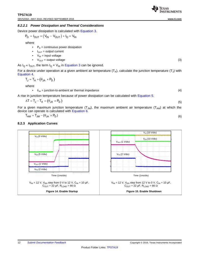
8.2.3 Application Curves
VIN = 12 V, VEN step from 0 V to 12 V, CIN = 10 µF,COUT = 22 µF, RLOAD = 66 Ω
Figure 14. Enable Startup
VIN = 12 V, VEN step from 12 V to 0 V, CIN = 10 µF,COUT = 22 µF, RLOAD = 66 Ω
Figure 15. Enable Shutdown
2
3
4
8
7
6
5
OUT
FB
GND
IN
DELAY
EN
CDELAY
Input Ground Plane
Output Ground Plane
PG
Notes: CIN and COUT are 1208 packages CDELAY, R1, and R2 are 0402 packages
Thermal
Pad
COUT
R2
Sense Line
VOUT
CIN
R1
Denotes a via to a connection made on another layer
1
VINGND
13
TPS7A19www.ti.com SBVS256A –MAY 2016–REVISED SEPTEMBER 2016
Product Folder Links: TPS7A19
Submit Documentation FeedbackCopyright © 2016, Texas Instruments Incorporated
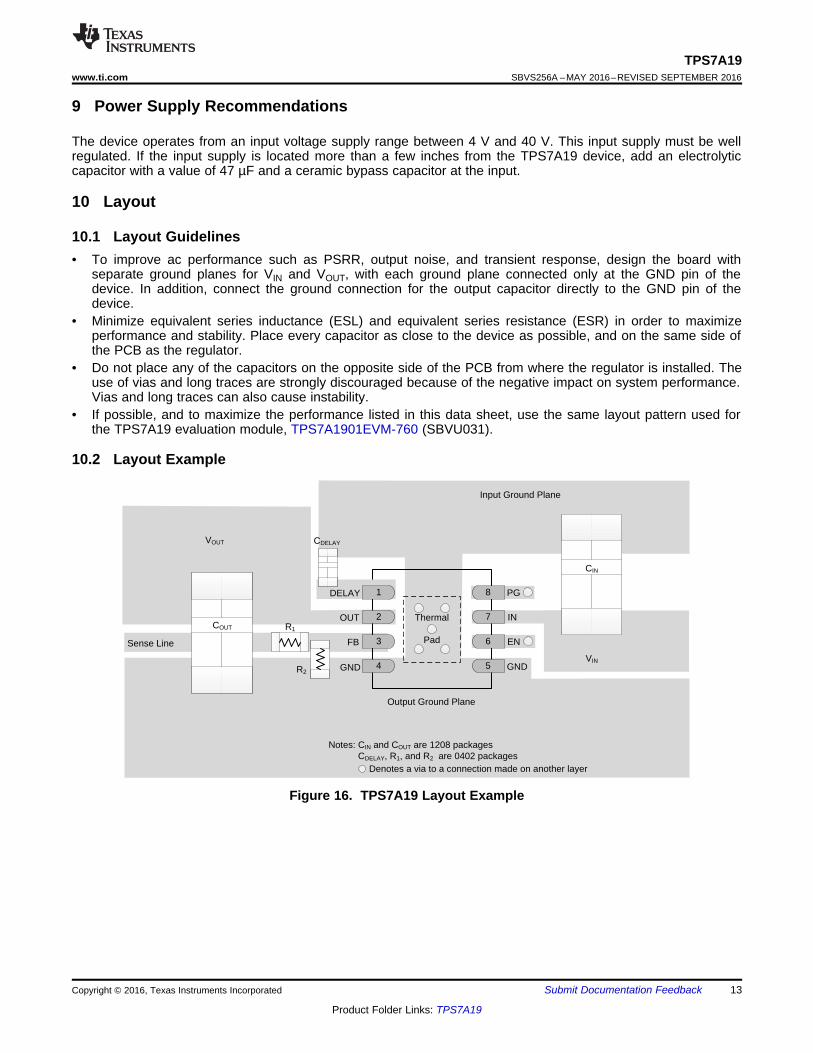
9 Power Supply Recommendations
The device operates from an input voltage supply range between 4 V and 40 V. This input supply must be wellregulated. If the input supply is located more than a few inches from the TPS7A19 device, add an electrolyticcapacitor with a value of 47 µF and a ceramic bypass capacitor at the input.
10 Layout
10.1 Layout Guidelines• To improve ac performance such as PSRR, output noise, and transient response, design the board with
separate ground planes for VIN and VOUT, with each ground plane connected only at the GND pin of thedevice. In addition, connect the ground connection for the output capacitor directly to the GND pin of thedevice.
• Minimize equivalent series inductance (ESL) and equivalent series resistance (ESR) in order to maximizeperformance and stability. Place every capacitor as close to the device as possible, and on the same side ofthe PCB as the regulator.
• Do not place any of the capacitors on the opposite side of the PCB from where the regulator is installed. Theuse of vias and long traces are strongly discouraged because of the negative impact on system performance.Vias and long traces can also cause instability.
• If possible, and to maximize the performance listed in this data sheet, use the same layout pattern used forthe TPS7A19 evaluation module, TPS7A1901EVM-760 (SBVU031).
10.2 Layout Example
Figure 16. TPS7A19 Layout Example

14
TPS7A19SBVS256A –MAY 2016–REVISED SEPTEMBER 2016 www.ti.com
Product Folder Links: TPS7A19
Submit Documentation Feedback Copyright © 2016, Texas Instruments Incorporated
11 Device and Documentation Support
11.1 Device Support
11.1.1 Development Support
11.1.1.1 Evaluation ModulesAn evaluation module (EVM) is available to assist in the initial circuit performance evaluation using the TPS7A19.The summary information for this fixture is shown in Table 2.
Table 2. Evaluation ModulesNAME EVM FOLDER
TPS7A19 40-V, 450-mA, High-Voltage, Ultra-Low IQ Low-Dropout Regulator Evaluation Module TPS7A1901EVM-760
(1) For the most current package and ordering information see the Package Option Addendum at the end of this document, or see thedevice product folder at www.ti.com.
11.1.1.2 Spice ModelsComputer simulation of circuit performance using SPICE is often useful when analyzing the performance ofanalog circuits and systems. A SPICE model for the TPS7A19 is available through the TPS7A19 product folderunder the tools and software tab.
11.1.2 Device Nomenclature
Table 3. Ordering Information (1)
PRODUCT DESCRIPTION
TPS7A19XXYYYZXX is the nominal output voltage option; 01 for adjustable.YYY is the package designator.Z is the package quantity.
11.2 Documentation Support
11.2.1 Related DocumentationTPS7A1901EVM-760 Evaluation Module User's Guide (SBVU031)
11.3 Receiving Notification of Documentation UpdatesTo receive notification of documentation updates, navigate to the device product folder on ti.com. In the upperright corner, click on Alert me to register and receive a weekly digest of any product information that haschanged. For change details, review the revision history included in any revised document.
11.4 Community ResourcesThe following links connect to TI community resources. Linked contents are provided "AS IS" by the respectivecontributors. They do not constitute TI specifications and do not necessarily reflect TI's views; see TI's Terms ofUse.
TI E2E™ Online Community TI's Engineer-to-Engineer (E2E) Community. Created to foster collaborationamong engineers. At e2e.ti.com, you can ask questions, share knowledge, explore ideas and helpsolve problems with fellow engineers.
Design Support TI's Design Support Quickly find helpful E2E forums along with design support tools andcontact information for technical support.
11.5 TrademarksE2E is a trademark of Texas Instruments.All other trademarks are the property of their respective owners.
15
TPS7A19www.ti.com SBVS256A –MAY 2016–REVISED SEPTEMBER 2016
Product Folder Links: TPS7A19
Submit Documentation FeedbackCopyright © 2016, Texas Instruments Incorporated
11.6 Electrostatic Discharge CautionThis integrated circuit can be damaged by ESD. Texas Instruments recommends that all integrated circuits be handled withappropriate precautions. Failure to observe proper handling and installation procedures can cause damage.
ESD damage can range from subtle performance degradation to complete device failure. Precision integrated circuits may be moresusceptible to damage because very small parametric changes could cause the device not to meet its published specifications.
11.7 GlossarySLYZ022 — TI Glossary.
This glossary lists and explains terms, acronyms, and definitions.
12 Mechanical, Packaging, and Orderable InformationThe following pages include mechanical, packaging, and orderable information. This information is the mostcurrent data available for the designated devices. This data is subject to change without notice and revision ofthis document. For browser-based versions of this data sheet, refer to the left-hand navigation.
PACKAGE OPTION ADDENDUM
www.ti.com 14-Oct-2016
Addendum-Page 1
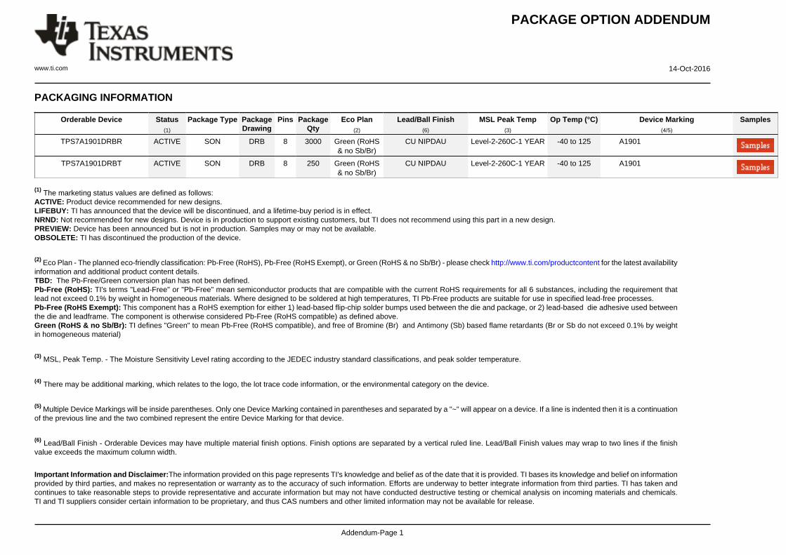
PACKAGING INFORMATION
Orderable Device Status(1)
Package Type PackageDrawing
Pins PackageQty
Eco Plan(2)
Lead/Ball Finish(6)
MSL Peak Temp(3)
Op Temp (°C) Device Marking(4/5)
Samples
TPS7A1901DRBR ACTIVE SON DRB 8 3000 Green (RoHS& no Sb/Br)
CU NIPDAU Level-2-260C-1 YEAR -40 to 125 A1901
TPS7A1901DRBT ACTIVE SON DRB 8 250 Green (RoHS& no Sb/Br)
CU NIPDAU Level-2-260C-1 YEAR -40 to 125 A1901
(1) The marketing status values are defined as follows:ACTIVE: Product device recommended for new designs.LIFEBUY: TI has announced that the device will be discontinued, and a lifetime-buy period is in effect.NRND: Not recommended for new designs. Device is in production to support existing customers, but TI does not recommend using this part in a new design.PREVIEW: Device has been announced but is not in production. Samples may or may not be available.OBSOLETE: TI has discontinued the production of the device.
(2) Eco Plan - The planned eco-friendly classification: Pb-Free (RoHS), Pb-Free (RoHS Exempt), or Green (RoHS & no Sb/Br) - please check http://www.ti.com/productcontent for the latest availabilityinformation and additional product content details.TBD: The Pb-Free/Green conversion plan has not been defined.Pb-Free (RoHS): TI's terms "Lead-Free" or "Pb-Free" mean semiconductor products that are compatible with the current RoHS requirements for all 6 substances, including the requirement thatlead not exceed 0.1% by weight in homogeneous materials. Where designed to be soldered at high temperatures, TI Pb-Free products are suitable for use in specified lead-free processes.Pb-Free (RoHS Exempt): This component has a RoHS exemption for either 1) lead-based flip-chip solder bumps used between the die and package, or 2) lead-based die adhesive used betweenthe die and leadframe. The component is otherwise considered Pb-Free (RoHS compatible) as defined above.Green (RoHS & no Sb/Br): TI defines "Green" to mean Pb-Free (RoHS compatible), and free of Bromine (Br) and Antimony (Sb) based flame retardants (Br or Sb do not exceed 0.1% by weightin homogeneous material)
(3) MSL, Peak Temp. - The Moisture Sensitivity Level rating according to the JEDEC industry standard classifications, and peak solder temperature.
(4) There may be additional marking, which relates to the logo, the lot trace code information, or the environmental category on the device.
(5) Multiple Device Markings will be inside parentheses. Only one Device Marking contained in parentheses and separated by a "~" will appear on a device. If a line is indented then it is a continuationof the previous line and the two combined represent the entire Device Marking for that device.
(6) Lead/Ball Finish - Orderable Devices may have multiple material finish options. Finish options are separated by a vertical ruled line. Lead/Ball Finish values may wrap to two lines if the finishvalue exceeds the maximum column width.
Important Information and Disclaimer:The information provided on this page represents TI's knowledge and belief as of the date that it is provided. TI bases its knowledge and belief on informationprovided by third parties, and makes no representation or warranty as to the accuracy of such information. Efforts are underway to better integrate information from third parties. TI has taken andcontinues to take reasonable steps to provide representative and accurate information but may not have conducted destructive testing or chemical analysis on incoming materials and chemicals.TI and TI suppliers consider certain information to be proprietary, and thus CAS numbers and other limited information may not be available for release.
PACKAGE OPTION ADDENDUM
www.ti.com 14-Oct-2016
Addendum-Page 2
In no event shall TI's liability arising out of such information exceed the total purchase price of the TI part(s) at issue in this document sold by TI to Customer on an annual basis.
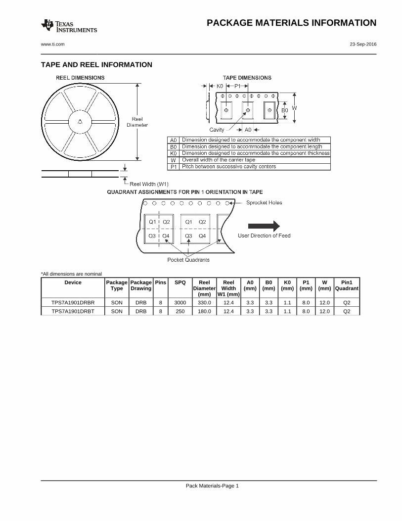
TAPE AND REEL INFORMATION
*All dimensions are nominal
Device PackageType
PackageDrawing
Pins SPQ ReelDiameter
(mm)
ReelWidth
W1 (mm)
A0(mm)
B0(mm)
K0(mm)
P1(mm)
W(mm)
Pin1Quadrant
TPS7A1901DRBR SON DRB 8 3000 330.0 12.4 3.3 3.3 1.1 8.0 12.0 Q2
TPS7A1901DRBT SON DRB 8 250 180.0 12.4 3.3 3.3 1.1 8.0 12.0 Q2
PACKAGE MATERIALS INFORMATION
www.ti.com 23-Sep-2016
Pack Materials-Page 1

*All dimensions are nominal
Device Package Type Package Drawing Pins SPQ Length (mm) Width (mm) Height (mm)
TPS7A1901DRBR SON DRB 8 3000 367.0 367.0 35.0
TPS7A1901DRBT SON DRB 8 250 210.0 185.0 35.0
PACKAGE MATERIALS INFORMATION
www.ti.com 23-Sep-2016
Pack Materials-Page 2


www.ti.com
PACKAGE OUTLINE
C
8X 0.350.25
2.4 0.052X
1.95
1.65 0.05
6X 0.65
1 MAX
8X 0.50.3
0.050.00
A 3.12.9
B
3.12.9
(0.2) TYP
VSON - 1 mm max heightDRB0008BPLASTIC SMALL OUTLINE - NO LEAD
4218876/A 12/2017
PIN 1 INDEX AREA
SEATING PLANE
0.08 C
1
4 5
8
(OPTIONAL)PIN 1 ID 0.1 C A B
0.05 C
THERMAL PADEXPOSED
NOTES: 1. All linear dimensions are in millimeters. Any dimensions in parenthesis are for reference only. Dimensioning and tolerancing per ASME Y14.5M. 2. This drawing is subject to change without notice. 3. The package thermal pad must be soldered to the printed circuit board for thermal and mechanical performance.
SCALE 4.000

www.ti.com
EXAMPLE BOARD LAYOUT
0.07 MINALL AROUND
0.07 MAXALL AROUND
8X (0.3)
(2.4)
(2.8)
6X (0.65)
(1.65)
( 0.2) VIATYP
(0.575)
(0.95)
8X (0.6)
(R0.05) TYP
VSON - 1 mm max heightDRB0008BPLASTIC SMALL OUTLINE - NO LEAD
4218876/A 12/2017
SYMM
1
45
8
LAND PATTERN EXAMPLESCALE:20X
NOTES: (continued) 4. This package is designed to be soldered to a thermal pad on the board. For more information, see Texas Instruments literature number SLUA271 (www.ti.com/lit/slua271).5. Vias are optional depending on application, refer to device data sheet. If any vias are implemented, refer to their locations shown on this view. It is recommended that vias under paste be filled, plugged or tented.
SOLDER MASKOPENINGSOLDER MASK
METAL UNDER
SOLDER MASKDEFINED
METALSOLDER MASKOPENING
SOLDER MASK DETAILS
NON SOLDER MASKDEFINED
(PREFERRED)

www.ti.com
EXAMPLE STENCIL DESIGN
(R0.05) TYP
8X (0.3)
8X (0.6)
(1.47)
(1.06)
(2.8)
(0.63)
6X (0.65)
VSON - 1 mm max heightDRB0008BPLASTIC SMALL OUTLINE - NO LEAD
4218876/A 12/2017
NOTES: (continued) 6. Laser cutting apertures with trapezoidal walls and rounded corners may offer better paste release. IPC-7525 may have alternate design recommendations.
SOLDER PASTE EXAMPLEBASED ON 0.125 mm THICK STENCIL
EXPOSED PAD
81% PRINTED SOLDER COVERAGE BY AREASCALE:25X
SYMM
1
4 5
8
METALTYP
SYMM

IMPORTANT NOTICE
Texas Instruments Incorporated (TI) reserves the right to make corrections, enhancements, improvements and other changes to itssemiconductor products and services per JESD46, latest issue, and to discontinue any product or service per JESD48, latest issue. Buyersshould obtain the latest relevant information before placing orders and should verify that such information is current and complete.TI’s published terms of sale for semiconductor products (http://www.ti.com/sc/docs/stdterms.htm) apply to the sale of packaged integratedcircuit products that TI has qualified and released to market. Additional terms may apply to the use or sale of other types of TI products andservices.Reproduction of significant portions of TI information in TI data sheets is permissible only if reproduction is without alteration and isaccompanied by all associated warranties, conditions, limitations, and notices. TI is not responsible or liable for such reproduceddocumentation. Information of third parties may be subject to additional restrictions. Resale of TI products or services with statementsdifferent from or beyond the parameters stated by TI for that product or service voids all express and any implied warranties for theassociated TI product or service and is an unfair and deceptive business practice. TI is not responsible or liable for any such statements.Buyers and others who are developing systems that incorporate TI products (collectively, “Designers”) understand and agree that Designersremain responsible for using their independent analysis, evaluation and judgment in designing their applications and that Designers havefull and exclusive responsibility to assure the safety of Designers' applications and compliance of their applications (and of all TI productsused in or for Designers’ applications) with all applicable regulations, laws and other applicable requirements. Designer represents that, withrespect to their applications, Designer has all the necessary expertise to create and implement safeguards that (1) anticipate dangerousconsequences of failures, (2) monitor failures and their consequences, and (3) lessen the likelihood of failures that might cause harm andtake appropriate actions. Designer agrees that prior to using or distributing any applications that include TI products, Designer willthoroughly test such applications and the functionality of such TI products as used in such applications.TI’s provision of technical, application or other design advice, quality characterization, reliability data or other services or information,including, but not limited to, reference designs and materials relating to evaluation modules, (collectively, “TI Resources”) are intended toassist designers who are developing applications that incorporate TI products; by downloading, accessing or using TI Resources in anyway, Designer (individually or, if Designer is acting on behalf of a company, Designer’s company) agrees to use any particular TI Resourcesolely for this purpose and subject to the terms of this Notice.TI’s provision of TI Resources does not expand or otherwise alter TI’s applicable published warranties or warranty disclaimers for TIproducts, and no additional obligations or liabilities arise from TI providing such TI Resources. TI reserves the right to make corrections,enhancements, improvements and other changes to its TI Resources. TI has not conducted any testing other than that specificallydescribed in the published documentation for a particular TI Resource.Designer is authorized to use, copy and modify any individual TI Resource only in connection with the development of applications thatinclude the TI product(s) identified in such TI Resource. NO OTHER LICENSE, EXPRESS OR IMPLIED, BY ESTOPPEL OR OTHERWISETO ANY OTHER TI INTELLECTUAL PROPERTY RIGHT, AND NO LICENSE TO ANY TECHNOLOGY OR INTELLECTUAL PROPERTYRIGHT OF TI OR ANY THIRD PARTY IS GRANTED HEREIN, including but not limited to any patent right, copyright, mask work right, orother intellectual property right relating to any combination, machine, or process in which TI products or services are used. Informationregarding or referencing third-party products or services does not constitute a license to use such products or services, or a warranty orendorsement thereof. Use of TI Resources may require a license from a third party under the patents or other intellectual property of thethird party, or a license from TI under the patents or other intellectual property of TI.TI RESOURCES ARE PROVIDED “AS IS” AND WITH ALL FAULTS. TI DISCLAIMS ALL OTHER WARRANTIES ORREPRESENTATIONS, EXPRESS OR IMPLIED, REGARDING RESOURCES OR USE THEREOF, INCLUDING BUT NOT LIMITED TOACCURACY OR COMPLETENESS, TITLE, ANY EPIDEMIC FAILURE WARRANTY AND ANY IMPLIED WARRANTIES OFMERCHANTABILITY, FITNESS FOR A PARTICULAR PURPOSE, AND NON-INFRINGEMENT OF ANY THIRD PARTY INTELLECTUALPROPERTY RIGHTS. TI SHALL NOT BE LIABLE FOR AND SHALL NOT DEFEND OR INDEMNIFY DESIGNER AGAINST ANY CLAIM,INCLUDING BUT NOT LIMITED TO ANY INFRINGEMENT CLAIM THAT RELATES TO OR IS BASED ON ANY COMBINATION OFPRODUCTS EVEN IF DESCRIBED IN TI RESOURCES OR OTHERWISE. IN NO EVENT SHALL TI BE LIABLE FOR ANY ACTUAL,DIRECT, SPECIAL, COLLATERAL, INDIRECT, PUNITIVE, INCIDENTAL, CONSEQUENTIAL OR EXEMPLARY DAMAGES INCONNECTION WITH OR ARISING OUT OF TI RESOURCES OR USE THEREOF, AND REGARDLESS OF WHETHER TI HAS BEENADVISED OF THE POSSIBILITY OF SUCH DAMAGES.Unless TI has explicitly designated an individual product as meeting the requirements of a particular industry standard (e.g., ISO/TS 16949and ISO 26262), TI is not responsible for any failure to meet such industry standard requirements.Where TI specifically promotes products as facilitating functional safety or as compliant with industry functional safety standards, suchproducts are intended to help enable customers to design and create their own applications that meet applicable functional safety standardsand requirements. Using products in an application does not by itself establish any safety features in the application. Designers mustensure compliance with safety-related requirements and standards applicable to their applications. Designer may not use any TI products inlife-critical medical equipment unless authorized officers of the parties have executed a special contract specifically governing such use.Life-critical medical equipment is medical equipment where failure of such equipment would cause serious bodily injury or death (e.g., lifesupport, pacemakers, defibrillators, heart pumps, neurostimulators, and implantables). Such equipment includes, without limitation, allmedical devices identified by the U.S. Food and Drug Administration as Class III devices and equivalent classifications outside the U.S.TI may expressly designate certain products as completing a particular qualification (e.g., Q100, Military Grade, or Enhanced Product).Designers agree that it has the necessary expertise to select the product with the appropriate qualification designation for their applicationsand that proper product selection is at Designers’ own risk. Designers are solely responsible for compliance with all legal and regulatoryrequirements in connection with such selection.Designer will fully indemnify TI and its representatives against any damages, costs, losses, and/or liabilities arising out of Designer’s non-compliance with the terms and provisions of this Notice.
Mailing Address: Texas Instruments, Post Office Box 655303, Dallas, Texas 75265Copyright © 2018, Texas Instruments Incorporated
Related Documents