White Paper 40-nm FPGA Power Management and Advantages December 2008, ver. 1.2 1 WP-01059-1.2 The 40-nm process offers clear benefits over prior nodes, including the 65-nm node and the more recent 45-nm node. One of the most attractive benefits is higher integration, which enables semiconductor manufacturers to pack greater functionality into less physical space at lower costs. Although increased density and performance are valuable benefits, one of the most pressing design considerations for today’s system developers is power consumption. To reduce power consumption, processing techniques go only so far. Smaller geometries provide the added benefit of reduced dynamic power consumption (less parasitic capacitances) but also raise standby power (increased leakage currents) unacceptably if no steps are taken to reduce it. Altera recognized this issue of increased power consumption and took aggressive steps to reduce both active and standby power. This white paper details the power saving architecture innovations in the core and I/Os, in addition to processing techniques used in Altera ® Stratix ® IV FPGAs to deliver the lowest power and the highest performance at the highest densities. Compared to the nearest competing FPGAs, Stratix IV FPGAs are over twice the density, 35 percent faster, and consume 50 percent less total power. Introduction Leakage current in digital logic is now the primary challenge for FPGAs as process geometries decrease. Static power consumption rises largely because of increases in various sources of leakage current. Figure 1 shows how these sources of leakage current (shown in blue) increase as the technology makes smaller gate lengths possible (shown in green). In addition, if no specific power optimization effort is made, dynamic power consumption can increase due to the greater logic capacity and higher switching frequencies that are attainable. Figure 1. Static Power Dissipation Increases Significantly at Smaller Process Geometries Power consumption is composed of static and dynamic power. Static power is the power consumed by the FPGA when it is programmed with a Programmer Object File (.pof) but no clocks are operating. Both digital and analog logic consume static power. In an analog system, static power is composed primarily of the quiescent current of the analog circuit based on its interface configuration. The sources of static leakage current in 40-nm devices are shown in Figure 2 and Table 1. Data from International Technology Roadmap for Semiconductors ITRS Roadmap Subthreshold leakage Gate-oxide leakage Technology node Power dissipation Physical gate length [nm] 1990 1995 2000 2005 2010 2015 2020 100 1 10 -2 10 -4 10 -6 300 250 200 150 100 50 0

Welcome message from author
This document is posted to help you gain knowledge. Please leave a comment to let me know what you think about it! Share it to your friends and learn new things together.
Transcript

White Paper
40-nm FPGA Power Management and Advantages
The 40-nm process offers clear benefits over prior nodes, including the 65-nm node and the more recent 45-nm node. One of the most attractive benefits is higher integration, which enables semiconductor manufacturers to pack greater functionality into less physical space at lower costs. Although increased density and performance are valuable benefits, one of the most pressing design considerations for today’s system developers is power consumption.
To reduce power consumption, processing techniques go only so far. Smaller geometries provide the added benefit of reduced dynamic power consumption (less parasitic capacitances) but also raise standby power (increased leakage currents) unacceptably if no steps are taken to reduce it. Altera recognized this issue of increased power consumption and took aggressive steps to reduce both active and standby power. This white paper details the power saving architecture innovations in the core and I/Os, in addition to processing techniques used in Altera® Stratix® IV FPGAs to deliver the lowest power and the highest performance at the highest densities. Compared to the nearest competing FPGAs, Stratix IV FPGAs are over twice the density, 35 percent faster, and consume 50 percent less total power.
Introduction Leakage current in digital logic is now the primary challenge for FPGAs as process geometries decrease. Static power consumption rises largely because of increases in various sources of leakage current. Figure 1 shows how these sources of leakage current (shown in blue) increase as the technology makes smaller gate lengths possible (shown in green). In addition, if no specific power optimization effort is made, dynamic power consumption can increase due to the greater logic capacity and higher switching frequencies that are attainable.
Figure 1. Static Power Dissipation Increases Significantly at Smaller Process Geometries
Power consumption is composed of static and dynamic power. Static power is the power consumed by the FPGA when it is programmed with a Programmer Object File (.pof) but no clocks are operating. Both digital and analog logic consume static power. In an analog system, static power is composed primarily of the quiescent current of the analog circuit based on its interface configuration. The sources of static leakage current in 40-nm devices are shown in Figure 2 and Table 1.
Data from International Technology Roadmap for Semiconductors ITRS Roadmap
Subthresholdleakage
Gate-oxideleakage
Technologynode
Pow
er d
issi
patio
n
Phys
ical
gat
e le
ngth
[nm
]
1990 1995 2000 2005 2010 2015 2020
100
1
10-2
10-4
10-6
300
250
200
150
100
50
0
December 2008, ver. 1.2 1
WP-01059-1.2

40-nm FPGA Power Management and Advantages Altera Corporation
Figure 2. Transistor Leakage Diagram
Dynamic power is the additional power consumed through the operation of the device caused by signals toggling and capacitive loads charging and discharging. As shown in Figure 3, the main variables affecting dynamic power are capacitance charging, the supply voltage, and the clock frequency. Dynamic power decreases with Moore’s law by taking advantage of process shrinks to reduce capacitance and voltage. The challenge is that as more circuits are implemented with each process shrink, the maximum clock frequency increases. While the power reduction declines for an equivalent circuit from process node to process node, the FPGA capacity doubles and the maximum clock frequency increases.
Figure 3. Variables Affecting Dynamic Power
Stratix IV Architecture and Processing Technology Power InnovationsAltera Stratix IV FPGAs attack these power challenges with core, I/O, and transceiver architecture innovations, along with the latest advancements in process technology and circuit techniques.
Programmable Power TechnologyFPGA cores fundamentally are made up of logic, memory, and digital signal processing (DSP) blocks. In standard FPGAs like Virtex-5 FPGAs, all of the blocks are designed to run at only one speed—the highest possible speed, as depicted by the yellow blocks in Figure 4—resulting in excessively high power consumption.
Table 1. Sources of Static Power
Source Impact Sensitivity Design TechniquesSubthreshold (weak inversion) leakage (ISUB) Dominant Supply voltage
Gate threshold voltageTemperatureChannel length
Reduced core voltageIncreased voltage thresholdIncreased gate lengths
Gate-induced drain leakage (IGIDL) Small Gate oxide thicknessSupply voltage
Dual gate oxide
Gate direct-tunneling leakage (IG) Small Gate oxide thicknessSupply voltage
Dual gate oxide
Reverse-biased junction leakage current (IREV) Negligible N/A to low voltageCMOS
None required
IG
IREV
Isub
IGIDL
n+ n+
GroundVDD
R
Pdynamic12---CV2 QShortCircuitV+ f activity⋅=
Capacitance charging Short circuit charge during switching
Percent of circuit that switches each cycle
2
Altera Corporation 40-nm FPGA Power Management and Advantages
Figure 4. Standard FPGA Fabric
Altera engineers analyzed benchmarks across 71 designs to evaluate the amount of high-speed logic that typically is required for a design. They compiled these designs to meet the highest performance that could be achieved within the FPGA fabric. Across these designs, the average amount of high-speed logic required was about 20 percent, as shown in Figure 5.
Figure 5. Benchmarks of High-Speed and Low-Power Logic Requirements
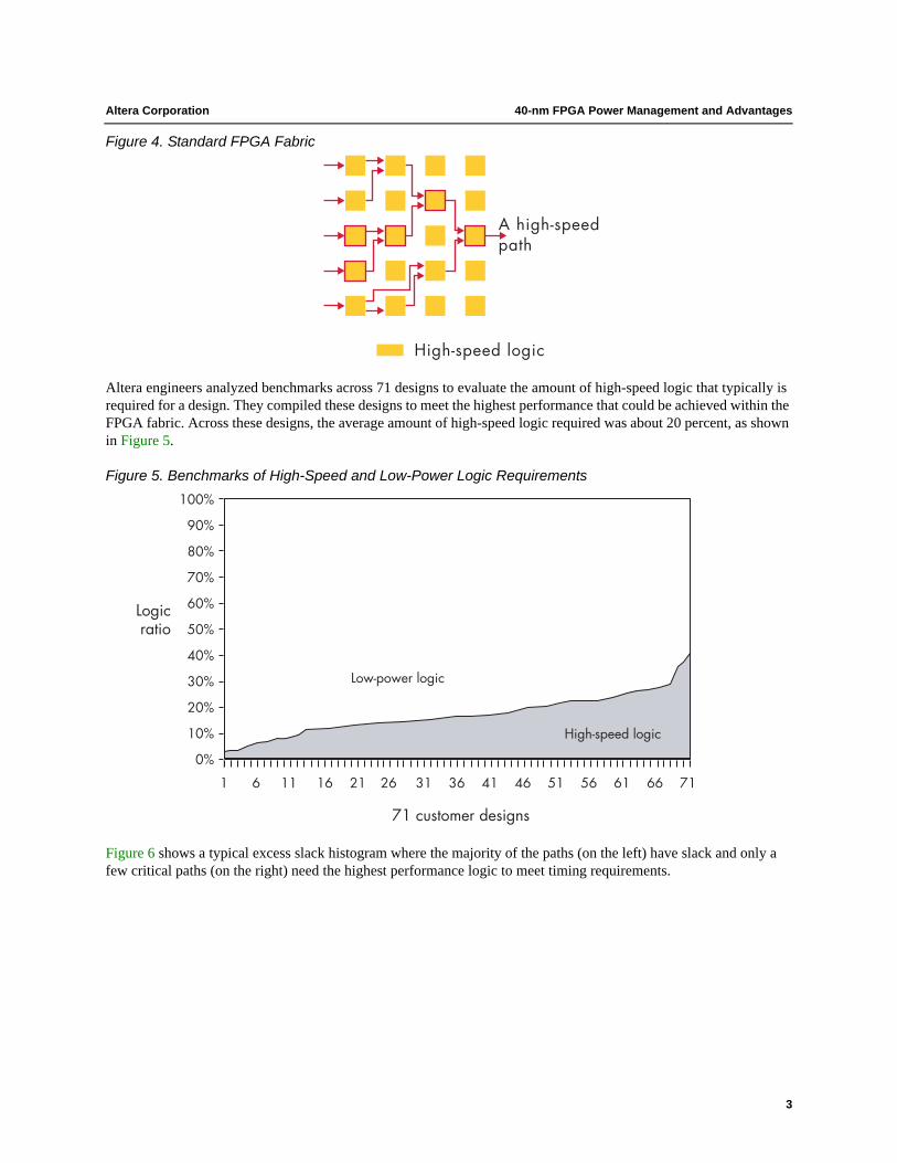
Figure 6 shows a typical excess slack histogram where the majority of the paths (on the left) have slack and only a few critical paths (on the right) need the highest performance logic to meet timing requirements.
A high-speedpath
High-speed logic
100%
90%
80%
70%
60%
50%
40%
30%
20%
10%
0%
Logicratio
71 customer designs
1 6 11 16 21 26 31 36 41 46 51 56 61 66 71
Low-power logic
High-speed logic
3
40-nm FPGA Power Management and Advantages Altera Corporation
Figure 6. Slack Histogram Showing a Small Number of Circuits With Little or No Slack
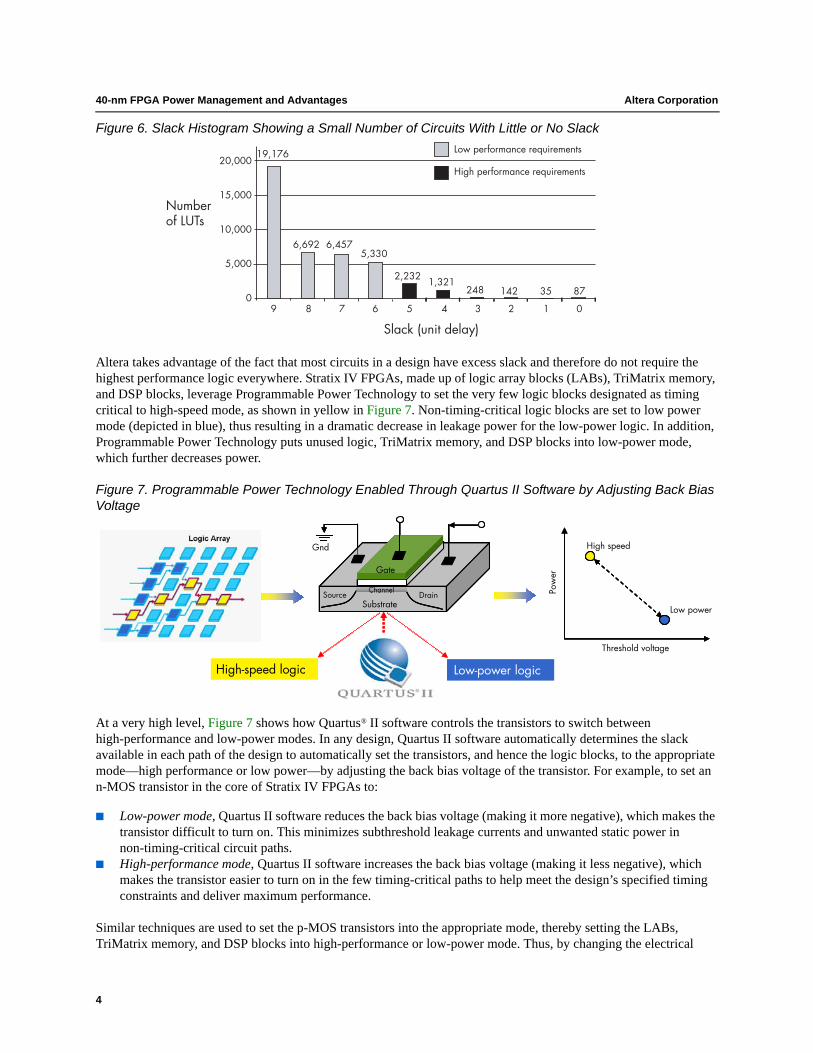
Altera takes advantage of the fact that most circuits in a design have excess slack and therefore do not require the highest performance logic everywhere. Stratix IV FPGAs, made up of logic array blocks (LABs), TriMatrix memory, and DSP blocks, leverage Programmable Power Technology to set the very few logic blocks designated as timing critical to high-speed mode, as shown in yellow in Figure 7. Non-timing-critical logic blocks are set to low power mode (depicted in blue), thus resulting in a dramatic decrease in leakage power for the low-power logic. In addition, Programmable Power Technology puts unused logic, TriMatrix memory, and DSP blocks into low-power mode, which further decreases power.
Figure 7. Programmable Power Technology Enabled Through Quartus II Software by Adjusting Back Bias Voltage
At a very high level, Figure 7 shows how Quartus® II software controls the transistors to switch between high-performance and low-power modes. In any design, Quartus II software automatically determines the slack available in each path of the design to automatically set the transistors, and hence the logic blocks, to the appropriate mode—high performance or low power—by adjusting the back bias voltage of the transistor. For example, to set an n-MOS transistor in the core of Stratix IV FPGAs to:
■ Low-power mode, Quartus II software reduces the back bias voltage (making it more negative), which makes the transistor difficult to turn on. This minimizes subthreshold leakage currents and unwanted static power in non-timing-critical circuit paths.
■ High-performance mode, Quartus II software increases the back bias voltage (making it less negative), which makes the transistor easier to turn on in the few timing-critical paths to help meet the design’s specified timing constraints and deliver maximum performance.
Similar techniques are used to set the p-MOS transistors into the appropriate mode, thereby setting the LABs, TriMatrix memory, and DSP blocks into high-performance or low-power mode. Thus, by changing the electrical
9 8 7 6 5 4 3 2 1 0
20,000
15,000
10,000
5,000
0
19,176
6,692 6,4575,330
2,232 1,321248 142 35 87
Low performance requirements
High performance requirements
Slack (unit delay)
Numberof LUTs
Pow
erHigh speed
Low power
Threshold voltage
SourceSubstrate
DrainChannel
Gnd
Gate
High Speed Logic Low Power Logic
Channel
GateGGaatee
Channel
Gate
High-speed logic Low-power logic
4
Altera Corporation 40-nm FPGA Power Management and Advantages
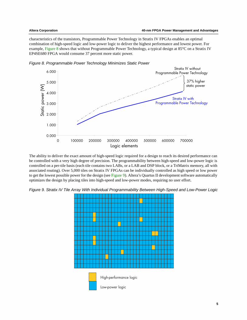
characteristics of the transistors, Programmable Power Technology in Stratix IV FPGAs enables an optimal combination of high-speed logic and low-power logic to deliver the highest performance and lowest power. For example, Figure 8 shows that without Programmable Power Technology, a typical design at 85°C on a Stratix IV EP4SE680 FPGA would consume 37 percent more static power.
Figure 8. Programmable Power Technology Minimizes Static Power
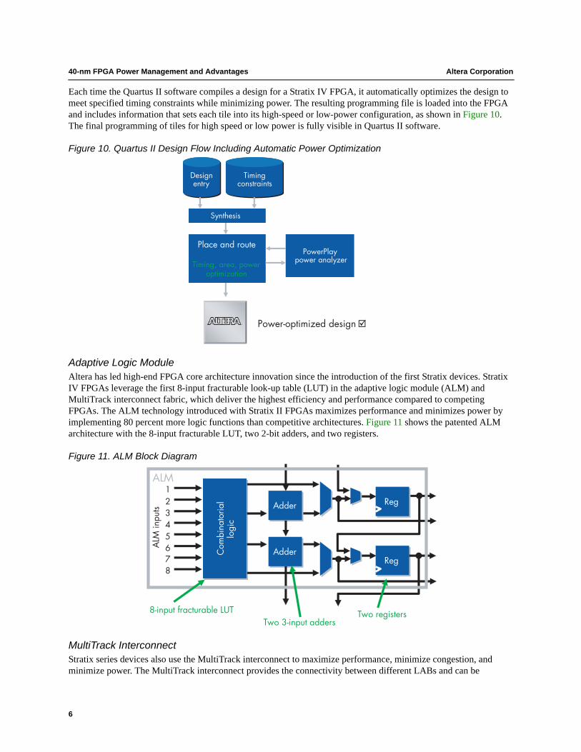
The ability to deliver the exact amount of high-speed logic required for a design to reach its desired performance can be controlled with a very high degree of precision. The programmability between high-speed and low-power logic is controlled on a per-tile basis (each tile contains two LABs, or a LAB and DSP block, or a TriMatrix memory, all with associated routing). Over 5,000 tiles on Stratix IV FPGAs can be individually controlled as high speed or low power to get the lowest possible power for the design (see Figure 9). Altera’s Quartus II development software automatically optimizes the design by placing tiles into high-speed and low-power modes, requiring no user effort.
Figure 9. Stratix IV Tile Array With Individual Programmability Between High-Speed and Low-Power Logic
0.000
1.000
2.000
3.000
4.000
5.000
6.000
0 100000 200000 300000 400000 500000 600000 700000
Stratix IV withoutProgrammable Power Technology
Stratix IV with Programmable Power Technology
37% higher static power
Logic elements
Stat
ic p
ower
(W)
High-performance logic
Low-power logic
5
40-nm FPGA Power Management and Advantages Altera Corporation
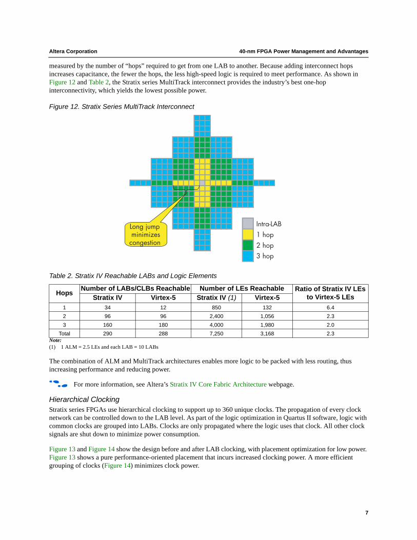
Each time the Quartus II software compiles a design for a Stratix IV FPGA, it automatically optimizes the design to meet specified timing constraints while minimizing power. The resulting programming file is loaded into the FPGA and includes information that sets each tile into its high-speed or low-power configuration, as shown in Figure 10. The final programming of tiles for high speed or low power is fully visible in Quartus II software.
Figure 10. Quartus II Design Flow Including Automatic Power Optimization
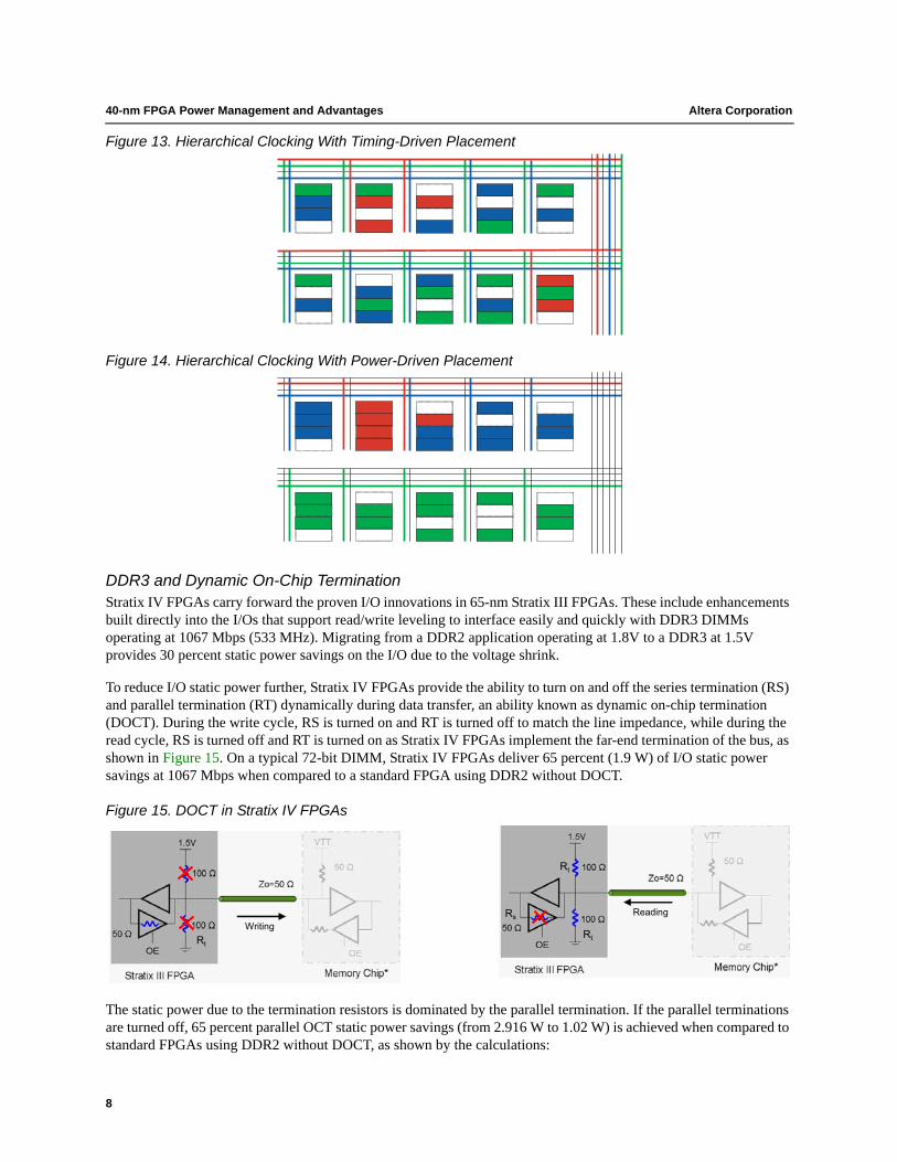
Adaptive Logic Module Altera has led high-end FPGA core architecture innovation since the introduction of the first Stratix devices. Stratix IV FPGAs leverage the first 8-input fracturable look-up table (LUT) in the adaptive logic module (ALM) and MultiTrack interconnect fabric, which deliver the highest efficiency and performance compared to competing FPGAs. The ALM technology introduced with Stratix II FPGAs maximizes performance and minimizes power by implementing 80 percent more logic functions than competitive architectures. Figure 11 shows the patented ALM architecture with the 8-input fracturable LUT, two 2-bit adders, and two registers.
Figure 11. ALM Block Diagram
MultiTrack Interconnect Stratix series devices also use the MultiTrack interconnect to maximize performance, minimize congestion, and minimize power. The MultiTrack interconnect provides the connectivity between different LABs and can be
DesignEntry
Designentry
TimingConstraints
Timingconstraints
SynthesisSynthesis
Place and Route
Timing, Area, PowerOptimization
Place and route
Timing, area, poweroptimization
PowerPlay Power Analyzer
PowerPlay power analyzer
Power-optimized design�
RegReg
RegReg
AdderAdder
AdderAdder
12345678
Com
bina
toria
llo
gic
ALM
inpu
ts
ALM
8-input fracturable LUTTwo 3-input adders
Two registers
6
Altera Corporation 40-nm FPGA Power Management and Advantages
measured by the number of “hops” required to get from one LAB to another. Because adding interconnect hops increases capacitance, the fewer the hops, the less high-speed logic is required to meet performance. As shown in Figure 12 and Table 2, the Stratix series MultiTrack interconnect provides the industry’s best one-hop interconnectivity, which yields the lowest possible power.
Figure 12. Stratix Series MultiTrack Interconnect
Note:(1) 1 ALM = 2.5 LEs and each LAB = 10 LABs
The combination of ALM and MultiTrack architectures enables more logic to be packed with less routing, thus increasing performance and reducing power.
f For more information, see Altera’s Stratix IV Core Fabric Architecture webpage.
Hierarchical ClockingStratix series FPGAs use hierarchical clocking to support up to 360 unique clocks. The propagation of every clock network can be controlled down to the LAB level. As part of the logic optimization in Quartus II software, logic with common clocks are grouped into LABs. Clocks are only propagated where the logic uses that clock. All other clock signals are shut down to minimize power consumption.
Figure 13 and Figure 14 show the design before and after LAB clocking, with placement optimization for low power. Figure 13 shows a pure performance-oriented placement that incurs increased clocking power. A more efficient grouping of clocks (Figure 14) minimizes clock power.
Table 2. Stratix IV Reachable LABs and Logic Elements
Hops Number of LABs/CLBs Reachable Number of LEs Reachable Ratio of Stratix IV LEs to Virtex-5 LEsStratix IV Virtex-5 Stratix IV (1) Virtex-5
1 34 12 850 132 6.42 96 96 2,400 1,056 2.33 160 180 4,000 1,980 2.0
Total 290 288 7,250 3,168 2.3
1 hop2 hop3 hop
Intra-LABLong jump minimizes congestion
7
40-nm FPGA Power Management and Advantages Altera Corporation
Figure 13. Hierarchical Clocking With Timing-Driven Placement
Figure 14. Hierarchical Clocking With Power-Driven Placement
DDR3 and Dynamic On-Chip TerminationStratix IV FPGAs carry forward the proven I/O innovations in 65-nm Stratix III FPGAs. These include enhancements built directly into the I/Os that support read/write leveling to interface easily and quickly with DDR3 DIMMs operating at 1067 Mbps (533 MHz). Migrating from a DDR2 application operating at 1.8V to a DDR3 at 1.5V provides 30 percent static power savings on the I/O due to the voltage shrink.
To reduce I/O static power further, Stratix IV FPGAs provide the ability to turn on and off the series termination (RS) and parallel termination (RT) dynamically during data transfer, an ability known as dynamic on-chip termination (DOCT). During the write cycle, RS is turned on and RT is turned off to match the line impedance, while during the read cycle, RS is turned off and RT is turned on as Stratix IV FPGAs implement the far-end termination of the bus, as shown in Figure 15. On a typical 72-bit DIMM, Stratix IV FPGAs deliver 65 percent (1.9 W) of I/O static power savings at 1067 Mbps when compared to a standard FPGA using DDR2 without DOCT.
Figure 15. DOCT in Stratix IV FPGAs
The static power due to the termination resistors is dominated by the parallel termination. If the parallel terminations are turned off, 65 percent parallel OCT static power savings (from 2.916 W to 1.02 W) is achieved when compared to standard FPGAs using DDR2 without DOCT, as shown by the calculations:
Rt
Rt
Rs
RtWriting
Reading
8
Altera Corporation 40-nm FPGA Power Management and Advantages
■ A 72-bit DDR2 application with 72 DQ and 18 DQS pins (in x4 mode) without DOCT consumes (# of pins × power per channel):
■ Moving the DDR2 application to DDR3 on Stratix IV FPGAs (without DOCT) consumes 30 percent less power:
■ Using DOCT with 50 percent read/write operation on a DDR3 application, the static power consumed is:
■ Taking the above calculations into consideration, the static-power reduction on Stratix IV FPGAs is 65 percent:
1 The power numbers shown in the calculation above do not include total I/O power but only represent the power savings seen by using DDR3 and DOCT. The total I/O power buffer power estimations in the early power estimator (EPE) spreadsheets show a static power reduction of 27 percent from 1.8V to 1.5V (3.581W to 2.630 W) and 64 percent savings overall (down to 1.636 W) when implementing the DDR3 application using 90 bidirectional pins writing 50 percent of the time.
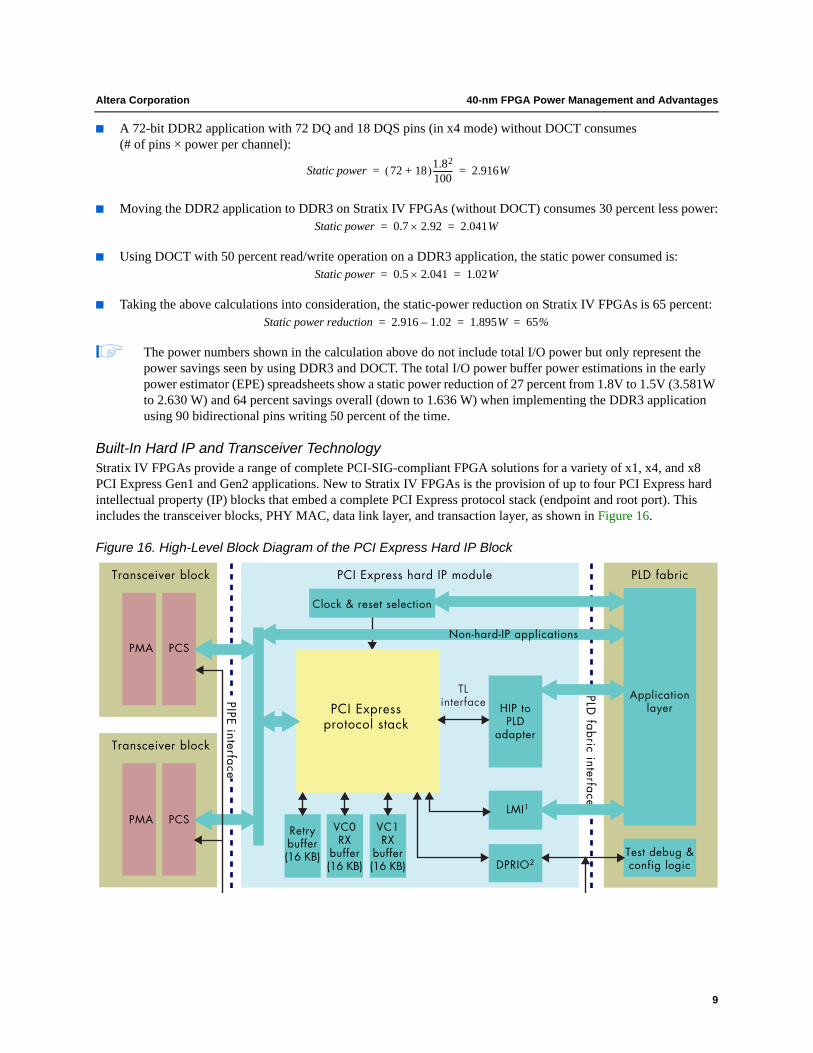
Built-In Hard IP and Transceiver TechnologyStratix IV FPGAs provide a range of complete PCI-SIG-compliant FPGA solutions for a variety of x1, x4, and x8 PCI Express Gen1 and Gen2 applications. New to Stratix IV FPGAs is the provision of up to four PCI Express hard intellectual property (IP) blocks that embed a complete PCI Express protocol stack (endpoint and root port). This includes the transceiver blocks, PHY MAC, data link layer, and transaction layer, as shown in Figure 16.
Figure 16. High-Level Block Diagram of the PCI Express Hard IP Block
Static power 72 18+( )1.82
100---------- 2.916W= =
Static power 0.7 2.92× 2.041W= =
Static power 0.5 2.041× 1.02W= =
Static power reduction 2.916 1.02– 1.895W 65%= = =
PLD fabric interface
PIPE interface
PCI Expressprotocol stack
HIP toPLD
adapter
LMI1
DPRIO2Test debug &config logic
Applicationlayer
Clock & reset selection
Retrybuffer(16 KB)
VC0RX
buffer(16 KB)
VC1RX
buffer(16 KB)
Transceiver block
PMA PCS
Transceiver block
PMA PCS
PLD fabricPCI Express hard IP module
TLinterface
Non-hard-IP applications
9
40-nm FPGA Power Management and Advantages Altera Corporation
In addition to the resource savings, embedded memory, shorter design- and compile-time savings, the hard IP core in Stratix IV FGPAs provides significant power savings when compared to the soft IP core implementation. See Table 3 for the power consumed by the PCI Express hard IP core Gen2 in Stratix IV FPGAs.
Note: (1) No competing FPGA has a Gen2 hard IP PCI Express core
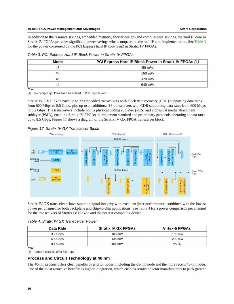
Stratix IV GX FPGAs have up to 32 embedded transceivers with clock data recovery (CDR) supporting data rates from 600 Mbps to 8.5 Gbps, plus up to an additional 16 transceivers with CDR supporting data rates from 600 Mbps to 3.2 Gbps. The transceivers include both a physical coding sublayer (PCS) and a physical media attachment sublayer (PMA), enabling Stratix IV FPGAs to implement standard and proprietary protocols operating at data rates up to 8.5 Gbps. Figure 17 shows a diagram of the Stratix IV GX FPGA transceiver block.
Figure 17. Stratix IV GX Transceiver Block
Stratix IV GX transceivers have superior signal integrity with excellent jitter performance, combined with the lowest power per channel for both backplane and chip-to-chip applications. See Table 4 for a power comparison per channel for the transceivers of Stratix IV FPGAs and the nearest competing device.
Note:(1) Virtex-5 does not offer 8.5 Gbps
Process and Circuit Technology at 40 nmThe 40-nm process offers clear benefits over prior nodes, including the 65-nm node and the more recent 45-nm node. One of the most attractive benefits is higher integration, which enables semiconductor manufacturers to pack greater
Table 3. PCI Express Hard IP Block Power in Stratix IV FPGAs
Mode PCI Express Hard IP Block Power in Stratix IV FPGAs (1)x1 80 mWx2 160 mWx4 320 mWx8 640 mW
Table 4. Stratix IV GX Transceiver Power
Data Rate Stratix IV GX FPGAs Virtex-5 FPGAs3.2 Gbps 100 mW ~100 mW6.5 Gbps 135 mW ~200 mW8.5 Gbps 165 mW NA (1)
Deskew
FIFO
Byte ordering
Word aligner
TXdata
RX PLL
TX PLL
PMA (analog)
RX PCS bypass
TX PCS Bypass
Transaction layer
Rate matching
FIFO
8b/1
0b decoder
Byte deserializer
RX phaseco
mp
ensa
tion
FIFO
PIPE interface
PIPE interface
RXdata
Clock recoveryunit
RX PLL
Bitserializer
Referenceclock
Referenceclock
Bitdeserializer
To FPGAlogic
PCS (digital) PIPE, PCIe hard IP
From FPGAlogic
Byte serializer
8b/1
0b encoder
PCIe hard IP
Transaction layer
PCIe hard IP
TX phasecco
mp
ensa
tion
FIFO
10
Altera Corporation 40-nm FPGA Power Management and Advantages
functionality into less physical space. In comparison to the 65-nm process, the 45-nm process delivers an improvement of twice the density, while the 40-nm process provides a 2.35X density improvement.
The semiconductor industry is constantly battling the evolving challenges of small process dimensions through huge investments in equipment, process technologies, design tools, and circuit techniques. The challenge of increasing leakage power with small process geometries is felt industry-wide, and a large number of widely used technologies at the 40-nm process node (and prior) are used to maintain or increase performance while managing leakage power. Altera continues to deliver leading-edge FPGAs using the latest industry capabilities, as shown in Table 5.
Copper Routing Altera switched to an all-copper metallization for on-chip routing beginning with the 150-nm process node, and used all-copper routing for all 130-nm, 90-nm, 65-nm, and 40-nm products, the earliest adoption in the FPGA industry. Copper replaced aluminum, providing reduced electrical and power resistance, and thereby increasing performance.
Low-k Dielectric A dielectric provides isolation between metal layers, enabling multiple routing layers. Moving to a low-k dielectric reduces the inter-routing layer capacitance, which significantly increases performance and reduces power. Altera was the first FPGA company to adopt the low-k process technology successfully.
Multi-Threshold TransistorsThe voltage threshold of a transistor affects the performance and leakage power of the transistor. Altera uses low-threshold voltages that produce high-speed transistors where performance is required and high-threshold voltages that produce slower, low-leakage transistors where performance is not required. Multi-threshold transistors were introduced in the 90-nm process node and carry forward to all of Altera’s latest FPGA offerings.
Variable Gate-Length TransistorsThe gate length of a transistor affects its speed and sub-threshold leakage. As the length of a transistor approaches the minimum gate length of the 40-nm process, the sub-threshold leakage current increases significantly. Altera uses longer gate lengths to reduce leakage current in circuits where performance is not required. Where performance is critical, Altera uses short gate lengths to maximize performance. Altera uses variable gate lengths to reduce power in 90-nm, 65-nm, and 40-nm Stratix series devices.
Triple Gate OxideThe thickness of the gate oxide affects the performance and leakage current of a transistor. Altera uses three separate oxides (triple gate oxide) across the I/O circuitry and core logic. In Stratix IV FPGAs, two of these core oxide thicknesses are used to enable low-performance transistors with minimum leakage, and high-performance transistors for maximum performance.
Table 5. Altera Process and Design Technique Adoption
Process or Design Technology When Introduced by Altera BenefitAll-copper routing 150 nm Increased performanceLow-k dielectric 130 nm Increased performance
Reduced powerMulti-threshold transistors 90 nm Reduced powerVariable gate-length transistors 90 nm Reduced powerTriple gate oxide 65 nm Reduced powerSuper-thin gate oxide 65 nm Increased performanceStrained silicon 65 nm Increased performance
11
40-nm FPGA Power Management and Advantages Altera Corporation
Super-Thin Gate OxideThe Stratix IV triple gate oxide technology includes a super-thin gate oxide for high-performance transistors. These transistors enable the use of longer gate lengths while still maximizing performance, significantly reducing subthreshold leakage for a modest increase in gate-induced drain leakage and gate-direct tunneling leakage.
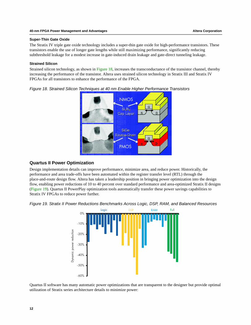
Strained Silicon Strained silicon technology, as shown in Figure 18, increases the transconductance of the transistor channel, thereby increasing the performance of the transistor. Altera uses strained silicon technology in Stratix III and Stratix IV FPGAs for all transistors to enhance the performance of the FPGA.
Figure 18. Strained Silicon Techniques at 40 nm Enable Higher Performance Transistors
Quartus II Power OptimizationDesign implementation details can improve performance, minimize area, and reduce power. Historically, the performance and area trade-offs have been automated within the register transfer level (RTL) through the place-and-route design flow. Altera has taken a leadership position in bringing power optimization into the design flow, enabling power reductions of 10 to 40 percent over standard performance and area-optimized Stratix II designs (Figure 19). Quartus II PowerPlay optimization tools automatically transfer these power savings capabilities to Stratix IV FPGAs to reduce power further.
Figure 19. Stratix II Power Reductions Benchmarks Across Logic, DSP, RAM, and Balanced Resources
Quartus II software has many automatic power optimizations that are transparent to the designer but provide optimal utilization of Stratix series architecture details to minimize power:
NMOS
PMOS
0%
-60%
-50%
-40%
-30%
-20%
-10%
Dyn
amic
pow
er re
duct
ion
Logic DSP RAM Full
12
Altera Corporation 40-nm FPGA Power Management and Advantages
■ Optimizations in analysis and synthesis that: ● Transform major functional blocks to map user RAMs so they use less power ● Restructure logic to reduce dynamic power and correctly select logic inputs to minimize capacitance on
high-toggling nets ■ Optimizations in fitter that:
● Reduce area and wiring demand for core logic to minimize dynamic power in routing ● Modify placement to reduce clocking power● Trade speed for reduced power when routing non-timing-critical data signals● Set tiles with timing critical paths to high-speed mode and all other tiles to low-power mode (Stratix III and
Stratix IV FPGAs)
Taking advantage of the Stratix IV low-power capabilities is seamless and automatic with Altera’s Quartus II development software. This software has set the standard for FPGA power technology with fully automatic power optimization and the most accurate power estimation from any vendor.
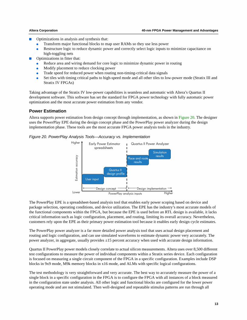
Power EstimationAltera supports power estimation from design concept through implementation, as shown in Figure 20. The designer uses the PowerPlay EPE during the design concept phase and the PowerPlay power analyzer during the design implementation phase. These tools are the most accurate FPGA power analysis tools in the industry.
Figure 20. PowerPlay Analysis Tools—Accuracy vs. Implementation
The PowerPlay EPE is a spreadsheet-based analysis tool that enables early power scoping based on device and package selection, operating conditions, and device utilization. The EPE has the industry’s most accurate models of the functional components within the FPGA, but because the EPE is used before an RTL design is available, it lacks critical information such as logic configuration, placement, and routing, limiting its overall accuracy. Nevertheless, customers rely upon the EPE as their primary power estimation tool because it enables early design cycle estimates.
The PowerPlay power analyzer is a far more detailed power analysis tool that uses actual design placement and routing and logic configuration, and can use simulated waveforms to estimate dynamic power very accurately. The power analyzer, in aggregate, usually provides ±15 percent accuracy when used with accurate design information.
Quartus II PowerPlay power models closely correlate to actual silicon measurements. Altera uses over 8,500 different test configurations to measure the power of individual components within a Stratix series device. Each configuration is focused on measuring a single circuit component of the FPGA in a specific configuration. Examples include DSP blocks in 9x9 mode, M9k memory blocks in x16 mode, and ALMs with specific logical configurations.
The test methodology is very straightforward and very accurate. The best way to accurately measure the power of a single block in a specific configuration in the FPGA is to configure the FPGA with all instances of a block measured in the configuration state under analysis. All other logic and functional blocks are configured for the lower power operating mode and are not stimulated. Then well-designed and repeatable stimulus patterns are run through all
Lower Higher
Higher
Estim
atio
n ac
cura
cy
PowerPlay analysis inputs
Design concept Design implementation
User input
Quartus II design profile
Place and routeresults
Simulation results
Early Power Estimator spreadsheets
Quartus II Power Analyzer
13

40-nm FPGA Power Management and Advantages Altera Corporation
instances of block measurement to generate a power profile. The resulting power consumed by the chip is largely the result of the large number of blocks under test, and the excess power can be subtracted from the total power. The resulting power, divided by the number of blocks configured, gives an accurate view of power for that mode of that block, as shown in Figure 21.
Figure 21. PowerPlay Power Estimate vs. Silicon Measurements for All RAM Configurations
ConclusionMigrating to smaller geometries delivers the expected Moore’s law benefits of increased density and performance, but to deliver the lowest power in conjunction with the highest performance, FPGA architectural innovations are needed beyond processing innovations. Unique technologies like Programmable Power Technology and DDR3 with DOCT enable Altera’s high-end FPGAs like Stratix IV FPGAs to deliver the lowest possible power without compromising on performance of next-generation designs.
Stratix IV FPGAs at 40-nm consume 50 percent less power and deliver 35 percent higher performance than the nearest competing high-end FPGAs. Figure 22 shows a power and performance comparison on the latest high-end FPGA offerings.
Figure 22. High-End FPGA Performance and Power Comparison
Quartus II design software offers the best power analysis and optimization in the FPGA industry by leveraging FPGA architectural innovations to automatically deliver the lowest power and highest performance on Stratix IV FPGAs. In addition, the Quartus II PowerPlay EPE enables designers to accurately model power on their system early on in the design cycle.
Dyn
amic
pow
er
RAM configuration
PowerPlay
Silicon
Stratix IV FPGAsVirtex-5 FPGAs
0.00
0.20
0.40
0.60
0.80
1.00
1.20
1.40
1.60
1.80
Slow
35%
Medium Fast
Rela
tive
FPG
A C
ore
Perfo
rman
ce
High-End FPGA Speed GradesStratix IVVirtex-5
1.0 -
0.5 -
Rela
tive
FPG
A T
ota
l Po
wer
50%Less Power
14
Altera Corporation 40-nm FPGA Power Management and Advantages
Copyright © 2008 Altera Corporation. All rights reserved. Altera, The Programmable Solutions Company, the stylized Altera logo, specific devicedesignations, and all other words and logos that are identified as trademarks and/or service marks are, unless noted otherwise, the trademarks and servicemarks of Altera Corporation in the U.S. and other countries. All other product or service names are the property of their respective holders. Altera productsare protected under numerous U.S. and foreign patents and pending applications, maskwork rights, and copyrights. Altera warrants performance of itssemiconductor products to current specifications in accordance with Altera's standard warranty, but reserves the right to make changes to any products andservices at any time without notice. Altera assumes no responsibility or liability arising out of the application or use of any information, product, or servicedescribed herein except as expressly agreed to in writing by Altera Corporation. Altera customers are advised to obtain the latest version of devicespecifications before relying on any published information and before placing orders for products or services.
101 Innovation DriveSan Jose, CA 95134www.altera.com
Further Information■ Altera at 40 nm: Jitter-, Signal Integrity-, Power-, and Process-Optimized Transceivers:
www.altera.com/literature/wp/wp-01057-stratix-iv-jitter-signal-integrity-optimized-transceivers.pdf■ Leveraging the 40-nm Process Node to Deliver the World’s Most Advanced Custom Logic Devices:
www.altera.com/literature/wp/wp-01058-stratix-iv-40nm-process-node-custom-logic-devices.pdf■ Increasing Productivity with Quartus II Incremental Compilation:
www.altera.com/literature/wp/wp-01062-quartus-ii-increasing-productivity-incremental-compilation.pdf■ “Standby and Active Leakage Current Control and Minimization in CMOS VLSI Circuits,” Farzan Fallah and
Massoud Pedram:http://atrak.usc.edu/~massoud/Papers/IEICE-leakage-review-journal.pdf
■ 40-nm FPGAs: Architecture and Performance Comparison:www.altera.com/literature/wp/wp-01088-40nm-architecture-performance-comparison.pdf
Acknowledgements■ Seyi Verma, Senior High-End Technical Analysis Staff, High-End FPGA Products, Altera Corporation
15
Related Documents