4.0 Design of Synchronous Counters This section begins our study of designing an important class of clocked sequential logic circuits-synchronous finite-state machines. Like all sequential circuits, a finite-state machine determines its outputs and its next state from its current inputs and current state. A synchronous finite- state machine changes state only on the clocking event. 4.1 General Model of a sequential Circuit The following diagram shows the general sequential circuit that consists of a combinational logic section and a memory section (flip -flops). The Combinational logic module is for us, as the designer, to match the design specifications. 4.2 Counter Design Procedure ?? Describe a general sequential circuit in terms of its basic parts and its input and outputs. ?? Develop a state diagram for a given sequence. ?? Develop a next-state table for a specific counter sequence. ?? Create a FF transition table. ?? Use K-map to derive the logic equations. ?? Implement a counter to produce a specified sequence of states.

Welcome message from author
This document is posted to help you gain knowledge. Please leave a comment to let me know what you think about it! Share it to your friends and learn new things together.
Transcript
4.0 Design of Synchronous Counters This section begins our study of designing an important class of clocked sequential logic circuits-synchronous finite-state machines. Like all sequential circuits, a finite-state machine determines its outputs and its next state from its current inputs and current state. A synchronous finite-state machine changes state only on the clocking event.
4.1 General Model of a sequential Circuit
The following diagram shows the general sequential circuit that consists of a combinational logic section and a memory section (flip-flops). The Combinational logic module is for us, as the designer, to match the design specifications.
4.2 Counter Design Procedure
?? Describe a general sequential circuit in terms of its basic parts and its input and outputs.
?? Develop a state diagram for a given sequence. ?? Develop a next-state table for a specific counter sequence. ?? Create a FF transition table. ?? Use K-map to derive the logic equations. ?? Implement a counter to produce a specified sequence of states.
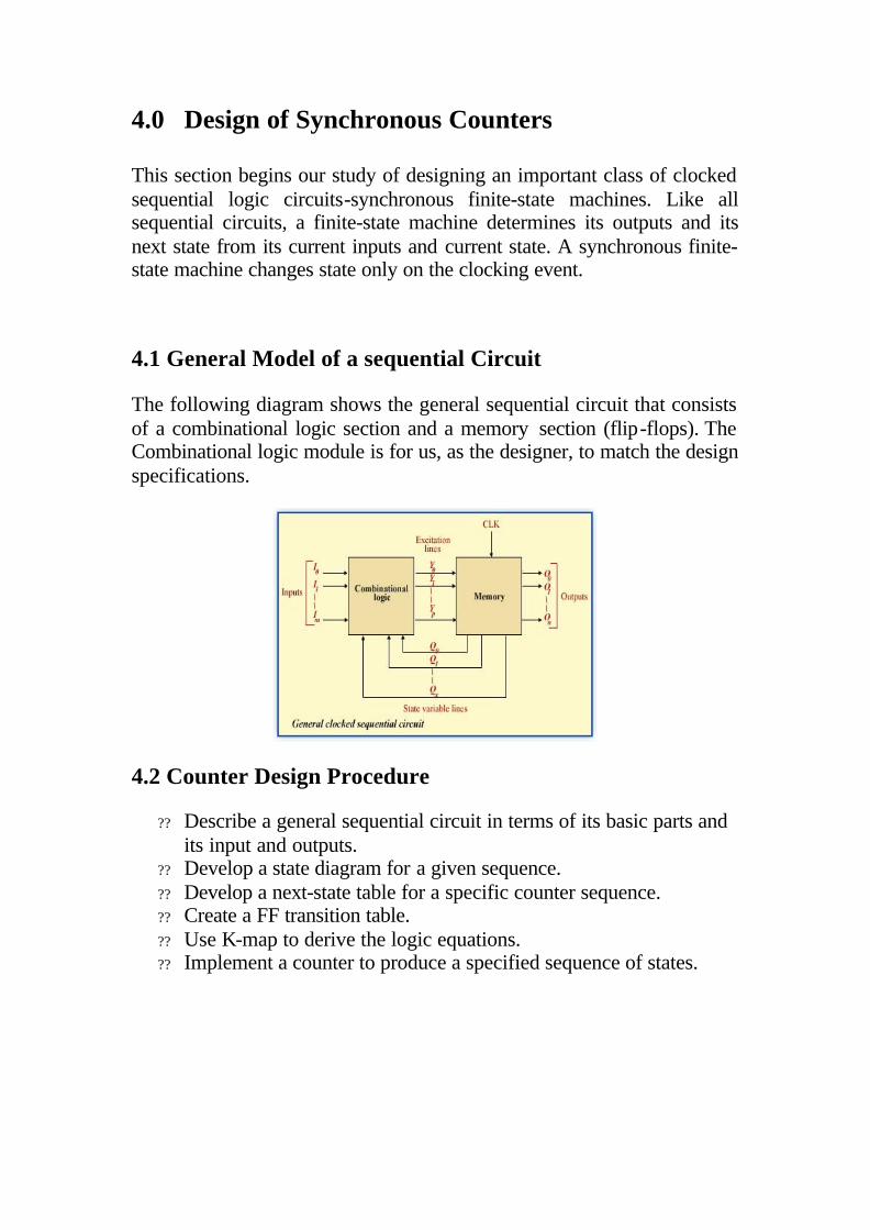
4.3. Design the 3-bit Gray code counter
Step 1: State Diagram
State Diagram for a 3-bit Gray code counter:
Step 2: Next-State Table
Next state table for a 3-bit Gray code counter
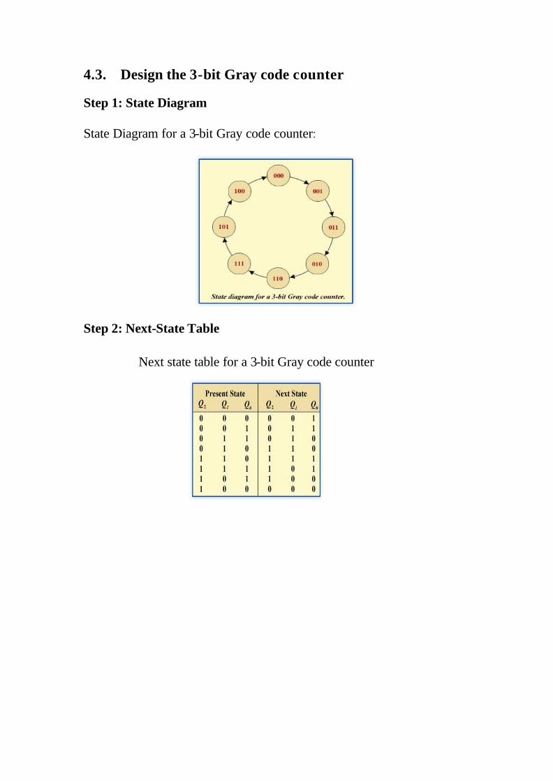
Step 3: Flip-Flop Transition Table
Transition table for a J-K Flip-Flop
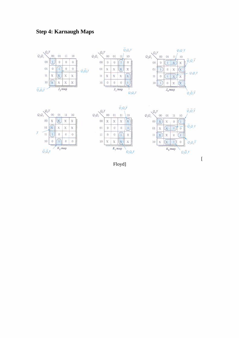
Step 4: Karnaugh Maps The following diagram shows the steps to create separate next states of separate J and K from the current states of J and K.
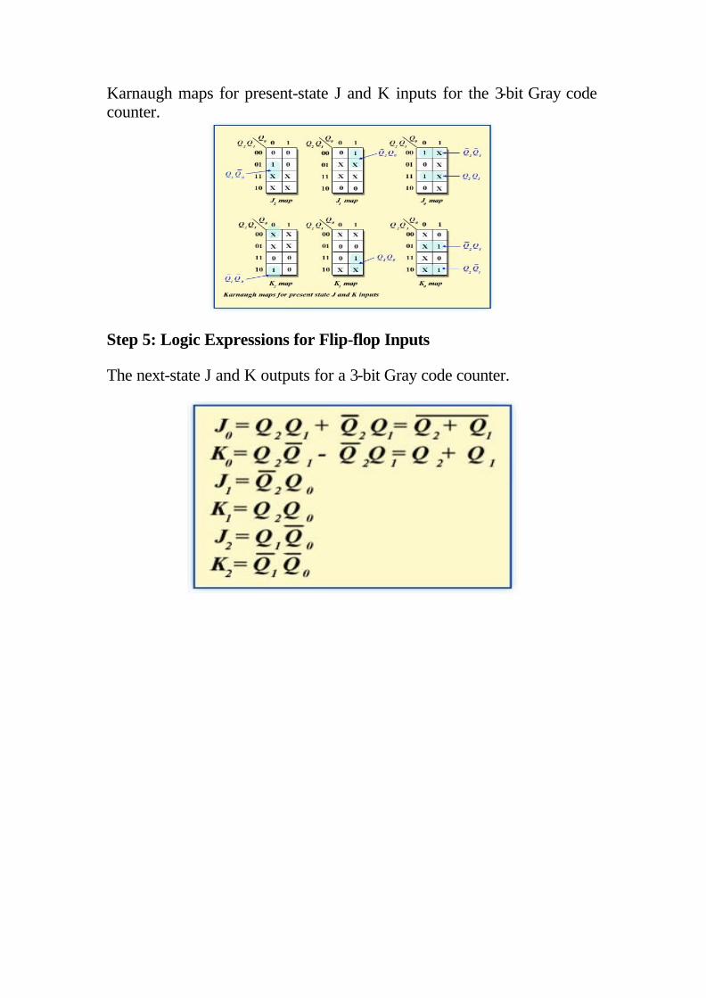
Karnaugh maps for present-state J and K inputs for the 3-bit Gray code counter.
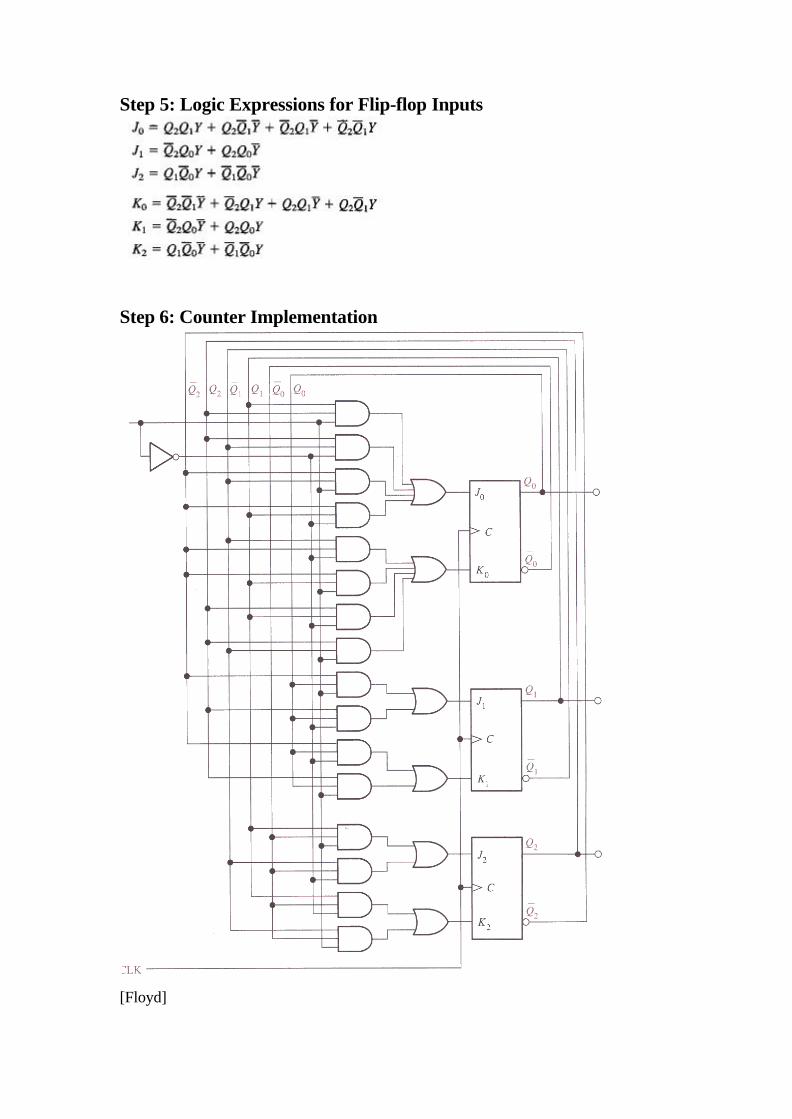
Step 5: Logic Expressions for Flip-flop Inputs
The next-state J and K outputs for a 3-bit Gray code counter.
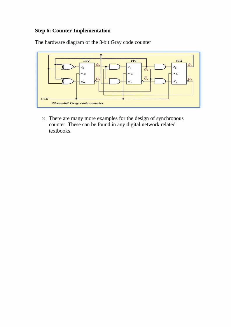
Step 6: Counter Implementation
The hardware diagram of the 3-bit Gray code counter
?? There are many more examples for the design of synchronous counter. These can be found in any digital network related textbooks.

4.4. Design – Example 1
Design a counter with the irregular binary count sequence shown in the state diagram of Figure 4.1. Step 1: State Diagram
Step 2: Next-State Table
Step 3: Flip-Flop Transition Table
Transition table for a J-K Flip-Flop
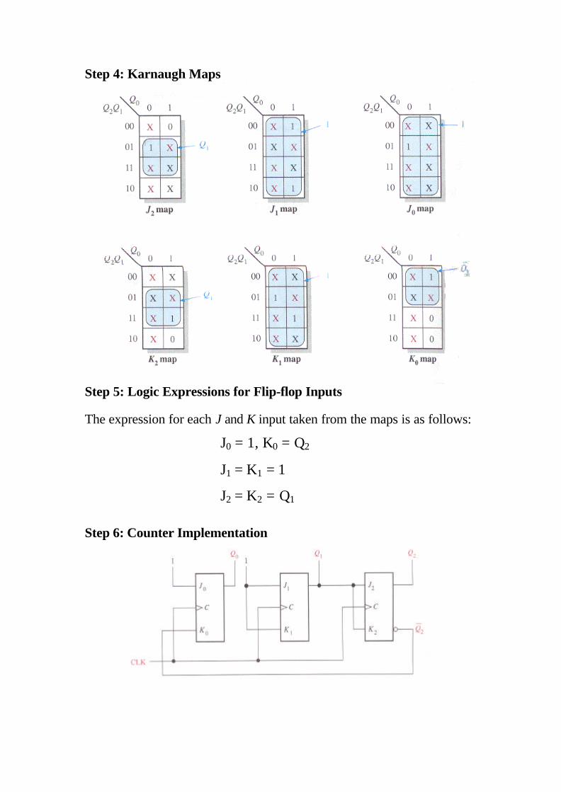
Step 4: Karnaugh Maps
Step 5: Logic Expressions for Flip-flop Inputs The expression for each J and K input taken from the maps is as follows:
J0 = 1, K0 = Q2
J1 = K1 = 1
J2 = K2 = Q1
Step 6: Counter Implementation
4.5. Example 2 - Design the 3 Up/down counter (Gray code sequence)
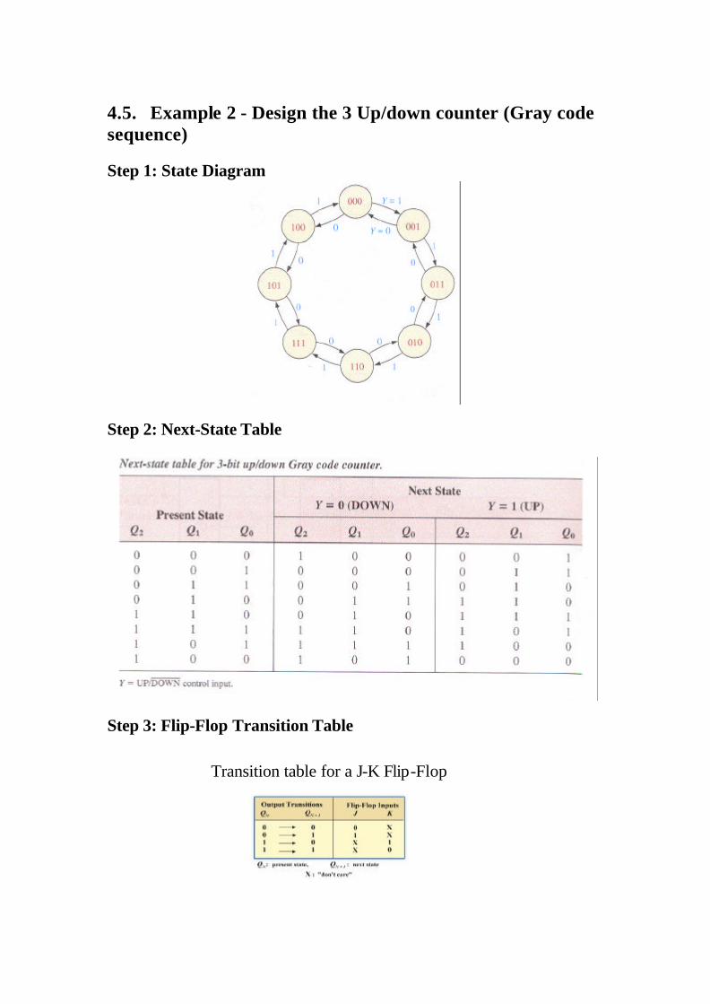
Step 1: State Diagram
Step 2: Next-State Table
Step 3: Flip-Flop Transition Table
Transition table for a J-K Flip-Flop
Step 4: Karnaugh Maps
[Floyd]
Step 5: Logic Expressions for Flip-flop Inputs
Step 6: Counter Implementation
[Floyd]
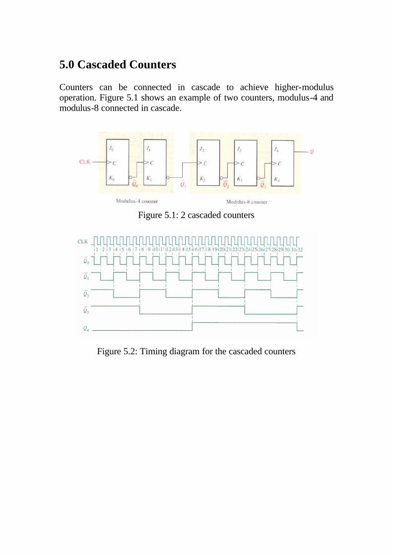
5.0 Cascaded Counters Counters can be connected in cascade to achieve higher-modulus operation. Figure 5.1 shows an example of two counters, modulus-4 and modulus-8 connected in cascade.
Figure 5.1: 2 cascaded counters
Figure 5.2: Timing diagram for the cascaded counters

5.1 Example 1: A modulus-100 counter Figure 5.3 illustrates a modulus-100 counter using 2 cascaded decade counters. This counter can be viewed as a frequency divider. It divides the input clock frequency by 100.
Figure 5.3: A modulus-100 counter using 2 cascaded decade counters 5.2 Example2: A modulus-1000 counter If you have a basis clock frequency of 1 MHz and you wish to obtain 100kHz, 10Hz, and 1kHz, a series of cascaded decade counters can be used. If 1 MHz signal is divided by 10, the output is 100kHz. Then if the 100 kHz signal is divided by 10, the output is 10kHz. Further division by 10 gives the 1 kHz frequency. The implementation is shown in Figure 5.4.
Figure 5.4: A modulus-1000 counter using 3 cascaded decade counters
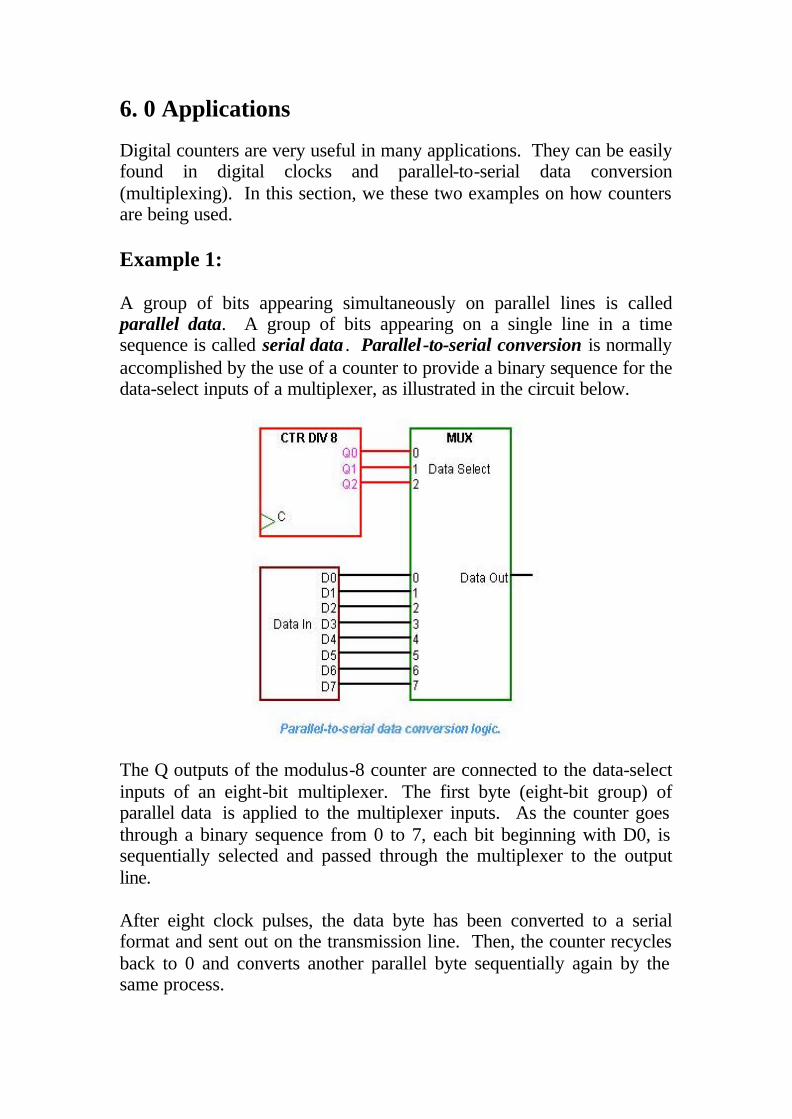
6. 0 Applications Digital counters are very useful in many applications. They can be easily found in digital clocks and parallel-to-serial data conversion (multiplexing). In this section, we these two examples on how counters are being used. Example 1: A group of bits appearing simultaneously on parallel lines is called parallel data. A group of bits appearing on a single line in a time sequence is called serial data . Parallel-to-serial conversion is normally accomplished by the use of a counter to provide a binary sequence for the data-select inputs of a multiplexer, as illustrated in the circuit below.
The Q outputs of the modulus-8 counter are connected to the data-select inputs of an eight-bit multiplexer. The first byte (eight-bit group) of parallel data is applied to the multiplexer inputs. As the counter goes through a binary sequence from 0 to 7, each bit beginning with D0, is sequentially selected and passed through the multiplexer to the output line. After eight clock pulses, the data byte has been converted to a serial format and sent out on the transmission line. Then, the counter recycles back to 0 and converts another parallel byte sequentially again by the same process.
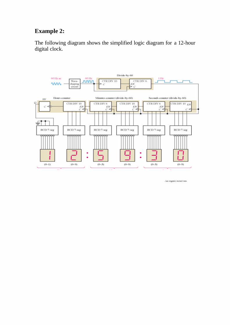
Example 2: The following diagram shows the simplified logic diagram for a 12-hour digital clock.
Related Documents