General Description The MAX6954 is a compact display driver that inter- faces microprocessors to a mix of 7-segment, 14-seg- ment, and 16-segment LED displays through an SPI™- or QSPI™-compatible 4-wire serial interface. The serial interface may be cascaded through multiple devices. The MAX6954 drives up to 16 digits 7-segment, 8 digits 14-segment, 8 digits 16-segment, or 128 discrete LEDs, while functioning from a supply voltage as low as 2.7V. The driver includes five I/O expander (or GPIO) lines, some or all of which may be configured as a key- switch reader, which automatically scans and debounces a matrix of up to 32 switches. Included on chip are full 14- and 16-segment ASCII 104-character fonts, a hexadecimal font for 7-segment displays, multiplex scan circuitry, anode and cathode drivers, and static RAM that stores each digit. The max- imum segment current for the display digits is set using a single external resistor. Digit intensity can be inde- pendently adjusted using the 16-step internal digital brightness control. The MAX6954 includes a low-power shutdown mode, a scan-limit register that allows the user to display from 1 to 16 digits, segment blinking (synchronized across multiple drivers, if desired), and a test mode, which forces all LEDs on. The LED drivers are slew-rate limited to reduce EMI. For a 2-wire interfaced version, refer to the MAX6955 data sheet. An evaluation kit (EV kit) for the MAX6955 is available. Applications Set-Top Boxes Automotive Panel Meters Bar Graph Displays White Goods Audio/Video Equipment Features ♦ High-Speed 26MHz SPI/QSPI/MICROWIRE™- Compatible Serial Interface ♦ 2.7V to 5.5V Operation ♦ Drives Up to 16 Digits 7-Segment, 8 Digits 14-Segment, 8 Digits 16-Segment, 128 Discrete LEDs, or a Combination of Digit Types ♦ Drives Common-Cathode Monocolor and Bicolor LED Displays ♦ Built-In ASCII 104-Character Font for 14-Segment and 16-Segment Digits and Hexadecimal Font for 7-Segment Digits ♦ Automatic Blinking Control for each Segment ♦ 10μA (typ) Low-Power Shutdown (Data Retained) ♦ 16-Step Digit-by-Digit Digital Brightness Control ♦ Display Blanked on Power-Up ♦ Slew-Rate Limited Segment Drivers for Lower EMI ♦ Five GPIO Port Pins Can Be Configured as Key- Switch Reader to Scan and Debounce Up to 32 Switches with n-Key Rollover ♦ IRQ Output when a Key Input Is Debounced ♦ 36-Pin SSOP and 40-Pin DIP and TQFN Packages ♦ Automotive Temperature Range Standard MAX6954 4-Wire Interfaced, 2.7V to 5.5V LED Display Driver with I/O Expander and Key Scan ________________________________________________________________ Maxim Integrated Products 1 Ordering Information 19-2460; Rev 4; 3/09 For pricing, delivery, and ordering information, please contact Maxim Direct at 1-888-629-4642, or visit Maxim’s website at www.maxim-ic.com. PART TEMP RANGE PIN-PACKAGE MAX6954AAX -40°C to +125°C 36 SSOP MAX6954APL -40°C to +125°C 40 PDIP MAX6954ATL+ -40°C to +125°C 40 TQFN-EP* SPI and QSPI are trademarks of Motorola, Inc. MICROWIRE is a trademark of National Semiconductor Corp. +Denotes a lead-free/RoHS-compliant package. *EP = Exposed pad. Pin Configurations and Typical Operating Circuits appear at end of data sheet. ISET OSC OSC_OUT BLINK CLK CS DIN DOUT 4-WIRE SERIAL INTERFACE RAM BLINK CONTROL CONFIGURATION REGISTER CHARACTER GENERATOR ROM CURRENT SOURCE DIVIDER/ COUNTER NETWORK DIGIT MULTIPLEXER PWM BRIGHTNESS CONTROL GPIO AND KEY-SCAN CONTROL LED DRIVERS O0 TO O23 P0 TO P4 MAX6954 Functional Diagram

Welcome message from author
This document is posted to help you gain knowledge. Please leave a comment to let me know what you think about it! Share it to your friends and learn new things together.
Transcript
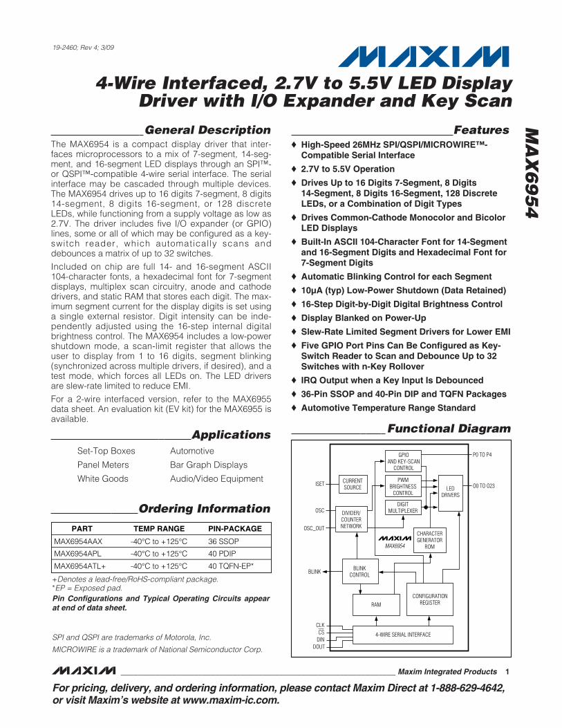
General DescriptionThe MAX6954 is a compact display driver that inter-faces microprocessors to a mix of 7-segment, 14-seg-ment, and 16-segment LED displays through an SPI™-or QSPI™-compatible 4-wire serial interface. The serialinterface may be cascaded through multiple devices.The MAX6954 drives up to 16 digits 7-segment, 8 digits14-segment, 8 digits 16-segment, or 128 discreteLEDs, while functioning from a supply voltage as low as2.7V. The driver includes five I/O expander (or GPIO)lines, some or all of which may be configured as a key-switch reader, which automatically scans anddebounces a matrix of up to 32 switches.
Included on chip are full 14- and 16-segment ASCII104-character fonts, a hexadecimal font for 7-segmentdisplays, multiplex scan circuitry, anode and cathodedrivers, and static RAM that stores each digit. The max-imum segment current for the display digits is set usinga single external resistor. Digit intensity can be inde-pendently adjusted using the 16-step internal digitalbrightness control. The MAX6954 includes a low-powershutdown mode, a scan-limit register that allows theuser to display from 1 to 16 digits, segment blinking(synchronized across multiple drivers, if desired), and atest mode, which forces all LEDs on. The LED driversare slew-rate limited to reduce EMI.
For a 2-wire interfaced version, refer to the MAX6955data sheet. An evaluation kit (EV kit) for the MAX6955 isavailable.
ApplicationsSet-Top Boxes Automotive
Panel Meters Bar Graph Displays
White Goods Audio/Video Equipment
Features♦ High-Speed 26MHz SPI/QSPI/MICROWIRE™-
Compatible Serial Interface
♦ 2.7V to 5.5V Operation
♦ Drives Up to 16 Digits 7-Segment, 8 Digits14-Segment, 8 Digits 16-Segment, 128 DiscreteLEDs, or a Combination of Digit Types
♦ Drives Common-Cathode Monocolor and BicolorLED Displays
♦ Built-In ASCII 104-Character Font for 14-Segmentand 16-Segment Digits and Hexadecimal Font for7-Segment Digits
♦ Automatic Blinking Control for each Segment
♦ 10µA (typ) Low-Power Shutdown (Data Retained)
♦ 16-Step Digit-by-Digit Digital Brightness Control
♦ Display Blanked on Power-Up
♦ Slew-Rate Limited Segment Drivers for Lower EMI
♦ Five GPIO Port Pins Can Be Configured as Key-Switch Reader to Scan and Debounce Up to 32Switches with n-Key Rollover
♦ IRQ Output when a Key Input Is Debounced
♦ 36-Pin SSOP and 40-Pin DIP and TQFN Packages
♦ Automotive Temperature Range Standard
MA
X6
95
4
4-Wire Interfaced, 2.7V to 5.5V LED DisplayDriver with I/O Expander and Key Scan
________________________________________________________________ Maxim Integrated Products 1
Ordering Information
19-2460; Rev 4; 3/09
For pricing, delivery, and ordering information, please contact Maxim Direct at 1-888-629-4642,or visit Maxim’s website at www.maxim-ic.com.
PART TEMP RANGE PIN-PACKAGE
MAX6954AAX -40°C to +125°C 36 SSOP
MAX6954APL -40°C to +125°C 40 PDIP
MAX6954ATL+ -40°C to +125°C 40 TQFN-EP*
SPI and QSPI are trademarks of Motorola, Inc.
MICROWIRE is a trademark of National Semiconductor Corp.
+Denotes a lead-free/RoHS-compliant package.*EP = Exposed pad.Pin Configurations and Typical Operating Circuits appearat end of data sheet.
ISET
OSC
OSC_OUT
BLINK
CLKCS
DINDOUT
4-WIRE SERIAL INTERFACE
RAM
BLINKCONTROL
CONFIGURATIONREGISTER
CHARACTERGENERATOR
ROM
CURRENTSOURCE
DIVIDER/COUNTERNETWORK
DIGITMULTIPLEXER
PWMBRIGHTNESS
CONTROL
GPIOAND KEY-SCAN
CONTROL
LEDDRIVERS
O0 TO O23
P0 TO P4
MAX6954
Functional Diagram
MA
X6
95
4
4-Wire Interfaced, 2.7V to 5.5V LED DisplayDriver with I/O Expander and Key Scan
2 _______________________________________________________________________________________
ABSOLUTE MAXIMUM RATINGS
Stresses beyond those listed under “Absolute Maximum Ratings” may cause permanent damage to the device. These are stress ratings only, and functionaloperation of the device at these or any other conditions beyond those indicated in the operational sections of the specifications is not implied. Exposure toabsolute maximum rating conditions for extended periods may affect device reliability.
(Voltage with respect to GND.)V+ .........................................................................-0.3V to +6VAll Other Pins............................................-0.3V to (V+ + 0.3V)
CurrentO0–O7 Sink Current ......................................................935mAO0–O18 Source Current .................................................55mADIN, CLK, CS, OSC, DOUT, BLINK, OSC_OUT, ISET ....20mAP0, P1, P2, P3, P4 ...........................................................40mAGND .....................................................................................1A
Continuous Power Dissipation (TA = +70°C)36-Pin SSOP (derate at 11.8mW/°C above +70°C) .....941mW40-Pin PDIP (derate at 16.7mW/°C above +70°C).....1333mW40-Pin TQFN (derate at 37mW/°C above +70°C) ......2963mW
Operating Temperature Range (TMIN to TMAX) ...............................................-40°C to +125°C
Junction Temperature ......................................................+150°CStorage Temperature Range .............................-65°C to +150°CLead Temperature (soldering, 10s) .................................+300°C
DC ELECTRICAL CHARACTERISTICS(Typical Operating Circuits, V+ = 2.7V to 5.5V, TA = TMIN to TMAX, unless otherwise noted.) (Note 1)
PARAMETER SYMBOL CONDITIONS MIN TYP MAX UNITS
Operating Supply Voltage V+ 2.7 5.5 V
TA = +25°C 10 35Shutdown Supply Current ISHDN
Shutdown mode, alldigital inputs at V+or GND TA = TMIN to TMAX 40
µA
TA = +25°C 22 30
Operating Supply Current I+
All segments on, alldigits scanned,intensity set to full,internal oscillator,DOUT open circuit,no display orOSC_OUT loadconnected
TA = TMIN to TMAX 35
mA
OSC = RC oscillator, RSET = 56kΩ,CSET = 22pF, V+ = 3.3V
4Master Clock Frequency fOSC
OSC driven externally 1 8
MHz
Dead Clock Protection Frequency fOSC 95 kHz
OSC Internal/External DetectionThreshold
VOSC 1.7 V
OSC High Time tCH 50 ns
OSC Low Time tCL 50 ns
Slow Segment Blink Period fSLOWBLINKOSC = RC oscillator, RSET = 56kΩ,CSET = 22pF, V+ = 3.3V 1 s
Fast Segment Blink Period fFASTBLINKOSC = RC oscillator, RSET = 56kΩ,CSET = 22pF, V+ = 3.3V
0.5 s
Fast or Slow Segment Blink DutyCycle
49.5 50.5 %
MA
X6
95
4
4-Wire Interfaced, 2.7V to 5.5V LED DisplayDriver with I/O Expander and Key Scan
_______________________________________________________________________________________ 3
DC ELECTRICAL CHARACTERISTICS (continued)(Typical Operating Circuits, V+ = 2.7V to 5.5V, TA = TMIN to TMAX, unless otherwise noted.) (Note 1)
PARAMETER SYMBOL CONDITIONS MIN TYP MAX UNITS
Segment Drive Source Current ISEGVLED = 2.2V,V+ = 3.3V
TA = +25°C -34.5 -40 -46.5 mA
Segment Current Slew Rate ΔISEG/Δt TA = +25°C, V+ = 3.3V 11 mA/µs
Segment Drive Current Matching ΔISEG TA = +25°C, V+ = 3.3V 5 10 %
LOGIC INPUTS AND OUTPUTS
Input Leakage CurrentDIN, CLK, CS, OSC, P0, P1, P2,P3, P4
IIH, IIL -1 +1 µA
4-Wire Logic-High Input VoltageDIN, CLK, CS
VIHSPI 1.8 V
4-Wire Logic-Low Input VoltageDIN, CLK, CS
VILSPI 0.6 V
Port Logic-High Input VoltageP0, P1, P2, P3, P4
VIHP0.7 xV+
V
Port Logic-Low Input VoltageP0, P1, P2, P3, P4
VILP0.3 xV+
V
Port Hysteresis Voltage P0, P1,P2, P3, P4
ΔVIP0.03 x
V+V
Port Input Pullup Current from V+ IIPUP0 to P3 configured as keyscan input, V+ =3.3V
75 µA
Port Output Low Voltage VOLP ISINK = 8mA 0.3 0.5 V
Blink Output Low Voltage VOLBK ISINK = 0.6mA 0.1 0.3 V
DOUT Output High Voltage VOHDO ISOURCE = 1.6mAV+ -0.2
V
DOUT Output Low Voltage VOLDO ISINK = 1.6mA 0.2 V
OSC_OUT Output High Voltage VOHOSC ISOURCE = 1.6mAV+ -0.4
V
OSC_OUT Output Low Voltage VOLOSC ISINK = 1.6mA 0.4 V
MA
X6
95
4
4-Wire Interfaced, 2.7V to 5.5V LED DisplayDriver with I/O Expander and Key Scan
4 _______________________________________________________________________________________
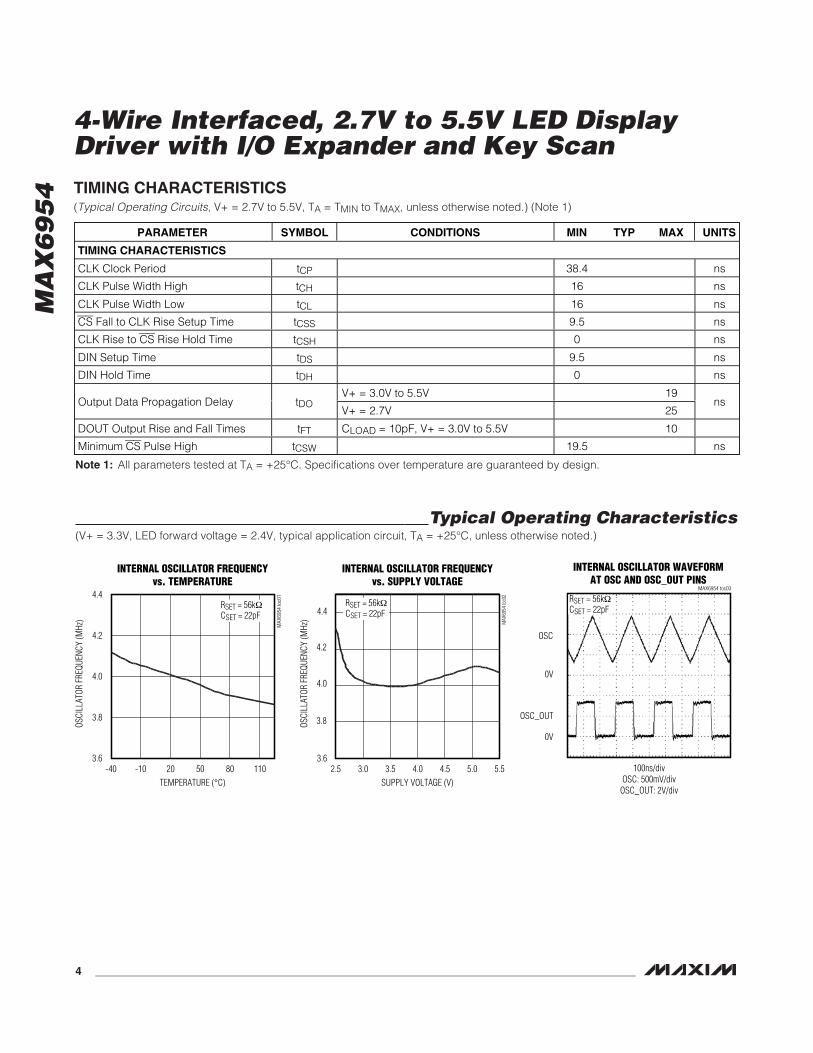
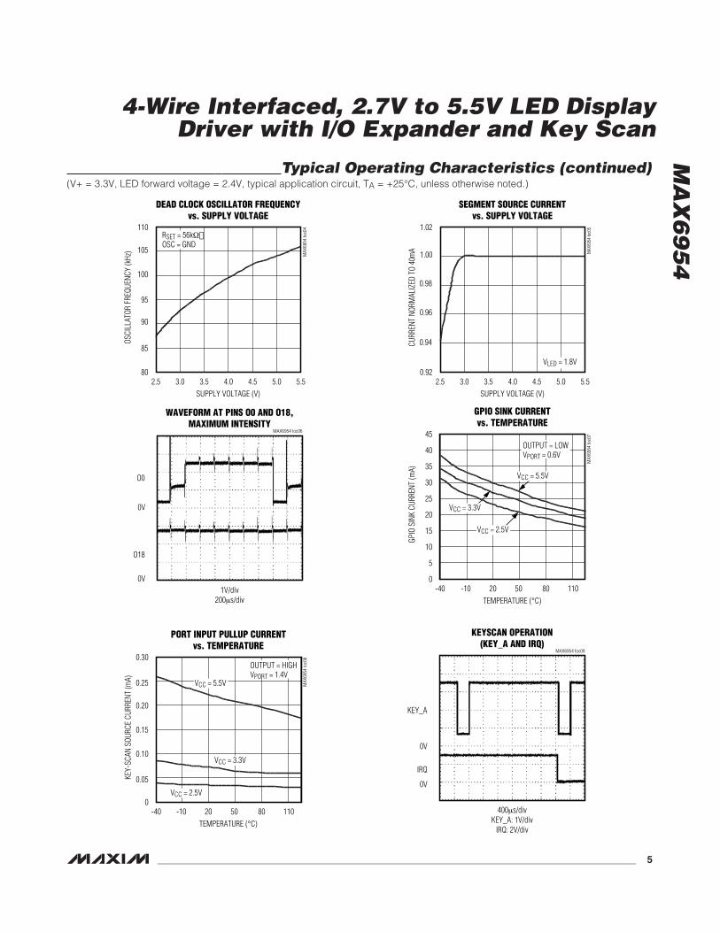
Typical Operating Characteristics(V+ = 3.3V, LED forward voltage = 2.4V, typical application circuit, TA = +25°C, unless otherwise noted.)
TIMING CHARACTERISTICS(Typical Operating Circuits, V+ = 2.7V to 5.5V, TA = TMIN to TMAX, unless otherwise noted.) (Note 1)
PARAMETER SYMBOL CONDITIONS MIN TYP MAX UNITS
TIMING CHARACTERISTICS
CLK Clock Period tCP 38.4 ns
CLK Pulse Width High tCH 16 ns
CLK Pulse Width Low tCL 16 ns
CS Fall to CLK Rise Setup Time tCSS 9.5 ns
CLK Rise to CS Rise Hold Time tCSH 0 ns
DIN Setup Time tDS 9.5 ns
DIN Hold Time tDH 0 ns
V+ = 3.0V to 5.5V 19Output Data Propagation Delay tDO
V+ = 2.7V 25ns
DOUT Output Rise and Fall Times tFT CLOAD = 10pF, V+ = 3.0V to 5.5V 10
Minimum CS Pulse High tCSW 19.5 ns
Note 1: All parameters tested at TA = +25°C. Specifications over temperature are guaranteed by design.
INTERNAL OSCILLATOR FREQUENCYvs. TEMPERATURE
MAX
6954
toc0
1
TEMPERATURE (°C)
OSCI
LLAT
OR F
REQU
ENCY
(MHz
)
110805020-10
3.8
4.0
4.2
4.4
3.6-40
RSET = 56k�CSET = 22pF
INTERNAL OSCILLATOR FREQUENCYvs. SUPPLY VOLTAGE
MAX
6954
toc0
2
SUPPLY VOLTAGE (V)
OSCI
LLAT
OR F
REQU
ENCY
(MHz
)
5.04.54.03.53.0
3.8
4.2
4.4
3.62.5 5.5
RSET = 56k�CSET = 22pF
4.0
100ns/divOSC: 500mV/div
OSC_OUT: 2V/div
MAX6954 toc03
OSC
0V
0V
OSC_OUT
INTERNAL OSCILLATOR WAVEFORMAT OSC AND OSC_OUT PINS
RSET = 56k�CSET = 22pF
MA
X6
95
4
4-Wire Interfaced, 2.7V to 5.5V LED DisplayDriver with I/O Expander and Key Scan
_______________________________________________________________________________________ 5
Typical Operating Characteristics (continued)(V+ = 3.3V, LED forward voltage = 2.4V, typical application circuit, TA = +25°C, unless otherwise noted.)
DEAD CLOCK OSCILLATOR FREQUENCYvs. SUPPLY VOLTAGE
MAX
6954
toc0
4
SUPPLY VOLTAGE (V)
OSCI
LLAT
OR F
REQU
ENCY
(kHz
)
5.04.54.03.53.0
85
95
105
110
802.5 5.5
RSET = 56k�OSC = GND
100
90
SEGMENT SOURCE CURRENTvs. SUPPLY VOLTAGE
MAX
6954
toc0
5
SUPPLY VOLTAGE (V)
CURR
ENT
NORM
ALIZ
ED T
O 40
mA
5.04.54.03.53.0
0.94
0.98
1.00
1.02
0.922.5 5.5
VLED = 1.8V
0.96
1V/div200μs/div
MAX6954 toc06
O0
O18
WAVEFORM AT PINS O0 AND O18,MAXIMUM INTENSITY
0V
0V
GPIO SINK CURRENTvs. TEMPERATURE
MAX
6954
toc0
7
TEMPERATURE (°C)
GPIO
SIN
K CU
RREN
T (m
A)
11050 8020-10
5
10
15
20
25
30
35
40
45
0-40
VCC = 3.3V
VCC = 2.5V
VCC = 5.5V
OUTPUT = LOWVPORT = 0.6V
PORT INPUT PULLUP CURRENTvs. TEMPERATURE
MAX
6954
toc0
8
TEMPERATURE (°C)
KEY-
SCAN
SOU
RCE
CURR
ENT
(mA)
11050 8020-10
0.05
0.10
0.15
0.20
0.25
0.30
0-40
VCC = 3.3V
VCC = 2.5V
VCC = 5.5V
OUTPUT = HIGHVPORT = 1.4V
400μs/divKEY_A: 1V/div
IRQ: 2V/div
MAX6954 toc09
KEY_A
0V
0V
IRQ
KEYSCAN OPERATION(KEY_A AND IRQ)
MA
X6
95
4
Detailed DescriptionThe MAX6954 is a serially interfaced display driver thatcan drive up to 16 digits 7-segment, 8 digits 14-seg-ment, 8 digits 16-segment, 128 discrete LEDs, or acombination of these display types. Table 1 shows thedrive capability of the MAX6954 for monocolor andbicolor displays.
The MAX6954 includes 104-character ASCII font mapsfor 14-segment and 16-segment displays, as well asthe hexadecimal font map for 7-segment displays. Thecharacters follow the standard ASCII font, with the addi-tion of the following common symbols: £, €, ¥, °, µ, ±,↑, and ↓. Seven bits represent the 104-character font
map; an 8th bit is used to select whether the decimalpoint (DP) is lit. Seven-segment LED digits may be con-trolled directly or use the hexadecimal font. Direct seg-ment control allows the MAX6954 to be used to drivebar graphs and discrete LED indicators.
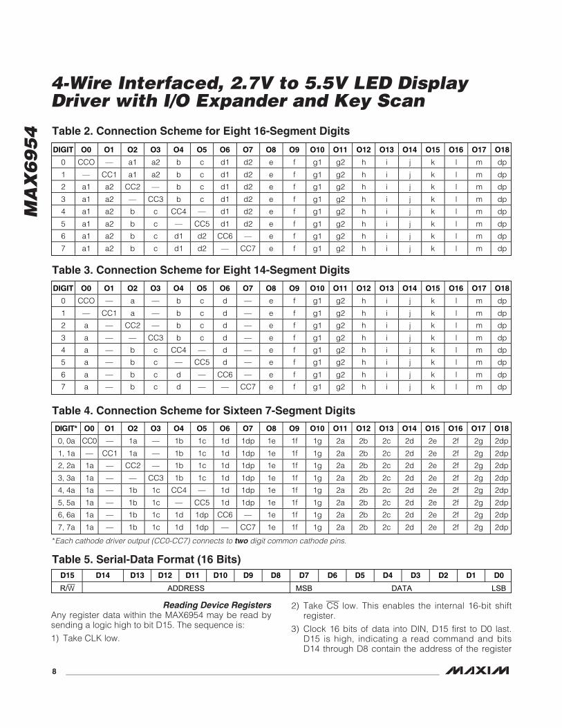
Tables 2, 3, and 4 list the connection schemes for 16-,14-, and 7-segment digits, respectively. The letters inTables 2, 3, and 4 correspond to the segment labelsshown in Figure 1. (For applications that require mixeddisplay types, see Tables 37–40.)
Serial InterfaceThe MAX6954 communicates through an SPI-compati-ble 4-wire serial interface. The interface has three
4-Wire Interfaced, 2.7V to 5.5V LED DisplayDriver with I/O Expander and Key Scan
6 _______________________________________________________________________________________
Pin Description
PIN
SSOP PDIP T Q F N - EPNAME FUNCTION
1, 2,34, 35, 36
1, 2,38, 39, 40
36, 37,33, 34, 35
P0–P4General-Purpose I/O Ports (GPIOs). GPIO can be configured as logic inputs oropen-drain outputs. Enabling key scanning configures some or all ports P0–P3 askey-switch matrix inputs with internal pullup and port P4 as IRQ output.
3 3 38 CSChip-Select Input. Serial data is loaded into the shift register while CS is low. Themost recent 16 bits of data latch on CS’s rising edge.
4 4 39 DOUTSerial-Data Output. The data into DIN is valid at DOUT 15.5 clock cycles later. Usethis pin to daisy-chain several devices or allow data readback. Output is push-pull.
5 5 40 CLKS er i al - C l ock Inp ut. On C LK’ s r i si ng ed g e, d ata shi fts i nto the i nter nal shi ft r eg i ster . OnC LK’ s fal l i ng ed g e, d ata i s cl ocked out of D OU T. C LK i s acti ve onl y w hi l e C S i s l ow .
6 6 1 DINSerial-Data Input. Data from DIN loads into the internal 16-bit shift register on CLK’srising edge.
7–15,22–31
7–15,26–35
2–10,21–30
O0–O18
Digit/Segment Drivers. When acting as digit drivers, outputs O0 to O7 sink currentfrom the display common cathodes. When acting as segment drivers, O0 to O18source current to the display anodes. O0 to O18 are high impedance when notbeing used as digit or segment drivers.
16, 18 17, 18, 20 12, 13, 15 GND Ground
17 19 14 ISETSegment Current Setting. Connect ISET to GND through series resistor RSET to setthe peak current.
19, 21 21, 23, 24 16, 18, 19 V+Positive Supply Voltage. Bypass V+ to GND with a 47µF bulk capacitor and a 0.1µFceramic capacitor.
20 22 17 OSCMultiplex Clock Input. To use internal oscillator, connect capacitor CSET from OSCto GND. To use external clock, drive OSC with a 1MHz to 8MHz CMOS clock.
32 36 31 BLINK Blink Clock Output. Output is open drain.
33 37 32 O S C _O U TClock Output. OSC_OUT is a buffered clock output to allow easy blinksynchronization of multiple MAX6954s. Output is push-pull.
— 16, 25 11, 20 N.C. Not Connected Internally
— — — EPExposed Pad (TQFN package only). Internally connected to GND. Connect to alarge ground plane to maximize thermal performance.

MA
X6
95
4
4-Wire Interfaced, 2.7V to 5.5V LED DisplayDriver with I/O Expander and Key Scan
_______________________________________________________________________________________ 7
inputs: clock (CLK), chip select (CS), and data in (DIN),and one output, data out (DOUT). CS must be low toclock data into or out of the device, and DIN must bestable when sampled on the rising edge of CLK. DOUTis stable on the rising edge of CLK. Note that while theSPI protocol expects DOUT to be high impedancewhen the MAX6954 is not being accessed, DOUT onthe MAX6954 is never high impedance.
CLK and DIN may be used to transmit data to otherperipherals. The MAX6954 ignores all activity on CLKand DIN except when CS is low.
Control and Operation Using the 4-Wire InterfaceControlling the MAX6954 requires sending a 16-bitword. The first byte, D15 through D8, is the command,and the second byte, D7 through D0, is the data byte(Table 5).
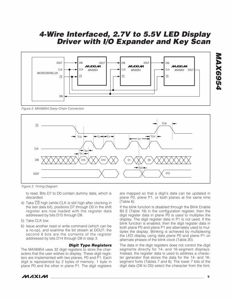
Connecting Multiple MAX6954s to the 4-Wire BusMultiple MAX6954s may be daisy-chained by connect-ing the DOUT of one device to the DIN of the next, anddriving CLK and CS lines in parallel (Figure 2). Data atDIN propagates through the internal shift registers andappears at DOUT 15.5 clock cycles later, clocked outon the falling edge of CLK. When sending commandsto daisy-chained MAX6954s, all devices are accessedat the same time. An access requires (16 x n) clockcycles, where n is the number of MAX6954s connected
together. To update just one device in a daisy-chain,the user can send the no-op command (0x00) to theothers. Figure 3 is the MAX6954 timing diagram.
The MAX6954 is written to using the followingsequence:
1) Take CLK low.
2) Take CS low. This enables the internal 16-bit shiftregister.
3) Clock 16 bits of data into DIN, D15 first to D0 last,observing the setup and hold times. Bit D15 is low,indicating a write command.
4) Take CS high (while CLK is still high after clocking inthe last data bit).
5) Take CLK low.
Figure 4 shows a write operation when 16 bits aretransmitted.
If fewer or greater than 16 bits are clocked into theMAX6954 between taking CS low and taking CS highagain, the MAX6954 stores the last 16 bits received,including the previous transmission(s). The generalcase is when n bits (where n > 16) are transmitted tothe MAX6954. The last bits are comprising bits {n-15} to{n}, are retained, and are parallel loaded into the 16-bitlatch as bits D15 to D0, respectively (Figure 5).
DISPLAY TYPE7 SEGMENT
(16-CHARACTERHEXADECIMAL FONT)
14 SEGMENT/16 SEGMENT
(104-CHARACTER ASCII FONT MAP)
DISCRETE LEDs(DIRECT CONTROL)
Monocolor 16 8 128
Bicolor 8 4 64
Table 1. MAX6954 Drive Capability
1dp 2dp
f b
e c
d1
a1
i
l
g1 g2
h j
m k
a2
d2
dp dp
1a
1g
1f 1b
1e 1c
1d
2a
2g
2f 2b
2e 2c
2d
f b
e c
d
a
i
l
g1 g2
h j
m k
Figure 1. Segment Labeling for 7-Segment Display, 14-Segment Display, and 16-Segment Display
MA
X6
95
4
4-Wire Interfaced, 2.7V to 5.5V LED DisplayDriver with I/O Expander and Key Scan
8 _______________________________________________________________________________________
Reading Device RegistersAny register data within the MAX6954 may be read bysending a logic high to bit D15. The sequence is:
1) Take CLK low.
2) Take CS low. This enables the internal 16-bit shiftregister.
3) Clock 16 bits of data into DIN, D15 first to D0 last.D15 is high, indicating a read command and bitsD14 through D8 contain the address of the register
DIGIT O0 O1 O2 O3 O4 O5 O6 O7 O8 O9 O10 O11 O12 O13 O14 O15 O16 O17 O18
0 CCO — a1 a2 b c d1 d2 e f g1 g2 h i j k l m dp
1 — CC1 a1 a2 b c d1 d2 e f g1 g2 h i j k l m dp
2 a1 a2 CC2 — b c d1 d2 e f g1 g2 h i j k l m dp
3 a1 a2 — CC3 b c d1 d2 e f g1 g2 h i j k l m dp
4 a1 a2 b c CC4 — d1 d2 e f g1 g2 h i j k l m dp
5 a1 a2 b c — CC5 d1 d2 e f g1 g2 h i j k l m dp
6 a1 a2 b c d1 d2 CC6 — e f g1 g2 h i j k l m dp
7 a1 a2 b c d1 d2 — CC7 e f g1 g2 h i j k l m dp
DIGIT O0 O1 O2 O3 O4 O5 O6 O7 O8 O9 O10 O11 O12 O13 O14 O15 O16 O17 O18
0 CCO — a — b c d — e f g1 g2 h i j k l m dp
1 — CC1 a — b c d — e f g1 g2 h i j k l m dp
2 a — CC2 — b c d — e f g1 g2 h i j k l m dp
3 a — — CC3 b c d — e f g1 g2 h i j k l m dp
4 a — b c CC4 — d — e f g1 g2 h i j k l m dp
5 a — b c — CC5 d — e f g1 g2 h i j k l m dp
6 a — b c d — CC6 — e f g1 g2 h i j k l m dp
7 a — b c d — — CC7 e f g1 g2 h i j k l m dp
Table 2. Connection Scheme for Eight 16-Segment Digits
Table 3. Connection Scheme for Eight 14-Segment Digits
D IG IT * O0 O1 O2 O3 O4 O5 O6 O7 O8 O9 O10 O11 O12 O13 O14 O15 O16 O17 O18
0, 0a C C 0 — 1a — 1b 1c 1d 1dp 1e 1f 1g 2a 2b 2c 2d 2e 2f 2g 2dp
1, 1a — CC1 1a — 1b 1c 1d 1dp 1e 1f 1g 2a 2b 2c 2d 2e 2f 2g 2dp
2, 2a 1a — CC2 — 1b 1c 1d 1dp 1e 1f 1g 2a 2b 2c 2d 2e 2f 2g 2dp
3, 3a 1a — — CC3 1b 1c 1d 1dp 1e 1f 1g 2a 2b 2c 2d 2e 2f 2g 2dp
4, 4a 1a — 1b 1c CC4 — 1d 1dp 1e 1f 1g 2a 2b 2c 2d 2e 2f 2g 2dp
5, 5a 1a — 1b 1c — CC5 1d 1dp 1e 1f 1g 2a 2b 2c 2d 2e 2f 2g 2dp
6, 6a 1a — 1b 1c 1d 1dp CC6 — 1e 1f 1g 2a 2b 2c 2d 2e 2f 2g 2dp
7, 7a 1a — 1b 1c 1d 1dp — CC7 1e 1f 1g 2a 2b 2c 2d 2e 2f 2g 2dp
Table 4. Connection Scheme for Sixteen 7-Segment Digits
D15 D14 D13 D12 D11 D10 D9 D8 D7 D6 D5 D4 D3 D2 D1 D0
R/W ADDRESS MSB DATA LSB
Table 5. Serial-Data Format (16 Bits)
*Each cathode driver output (CC0-CC7) connects to two digit common cathode pins.
MA
X6
95
4
4-Wire Interfaced, 2.7V to 5.5V LED DisplayDriver with I/O Expander and Key Scan
_______________________________________________________________________________________ 9
to read. Bits D7 to D0 contain dummy data, which isdiscarded.
4) Take CS high (while CLK is still high after clocking inthe last data bit), positions D7 through D0 in the shiftregister are now loaded with the register dataaddressed by bits D15 through D8.
5) Take CLK low.
6) Issue another read or write command (which can bea no-op), and examine the bit stream at DOUT; thesecond 8 bits are the contents of the registeraddressed by bits D14 through D8 in step 3.
Digit Type RegistersThe MAX6954 uses 32 digit registers to store the char-acters that the user wishes to display. These digit regis-ters are implemented with two planes, P0 and P1. Eachdigit is represented by 2 bytes of memory, 1 byte inplane P0 and the other in plane P1. The digit registers
are mapped so that a digit’s data can be updated inplane P0, plane P1, or both planes at the same time(Table 6).
If the blink function is disabled through the Blink EnableBit E (Table 19) in the configuration register, then thedigit register data in plane P0 is used to multiplex thedisplay. The digit register data in P1 is not used. If theblink function is enabled, then the digit register data inboth plane P0 and plane P1 are alternately used to mul-tiplex the display. Blinking is achieved by multiplexingthe LED display using data plane P0 and plane P1 onalternate phases of the blink clock (Table 20).
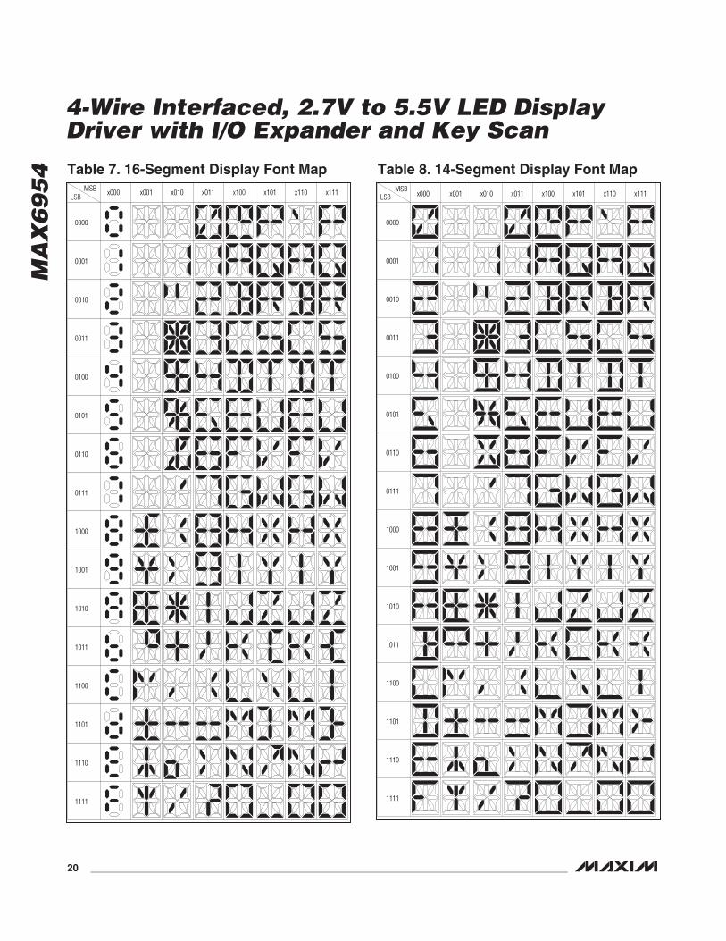
The data in the digit registers does not control the digitsegments directly for 14- and 16-segment displays.Instead, the register data is used to address a charac-ter generator that stores the data for the 14- and 16-segment fonts (Tables 7 and 8). The lower 7 bits of thedigit data (D6 to D0) select the character from the font.
tCSS tCL tCHtCP
tCSH
tCSW
tDStDH
D15
CLK
DIN
CS
D14 D1 D0
D15
tDO
DOUT
Figure 3. Timing Diagram
MAX6954
DOUT
MICROCONTROLLERCLK
DIN
MAX6954 MAX6954CLK
DIN
CS
DOUT
CLK
DIN
CS
DOUT
CLK
DIN
CS
DOUT
CS
Figure 2. MAX6954 Daisy-Chain Connection

MA
X6
95
4
4-Wire Interfaced, 2.7V to 5.5V LED DisplayDriver with I/O Expander and Key Scan
10 ______________________________________________________________________________________
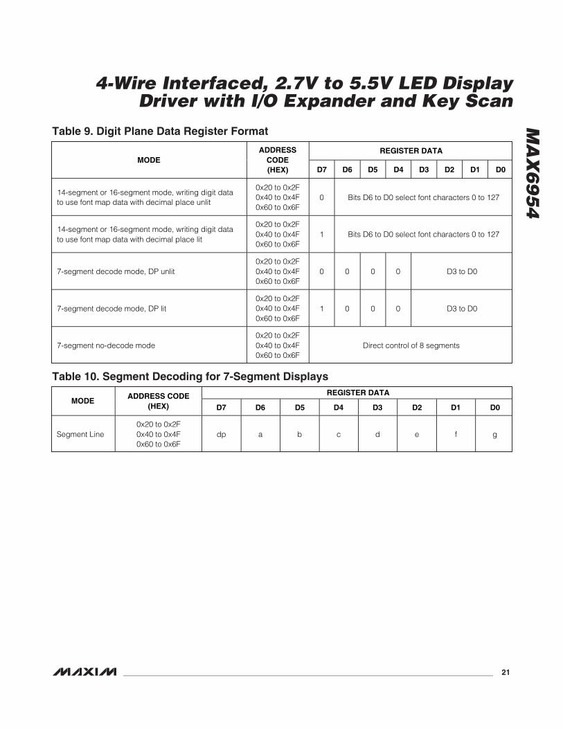
The most significant bit of the register data (D7) con-trols the DP segment of the digits; it is set to 1 to lightDP, and to zero to leave DP unlit (Table 9).
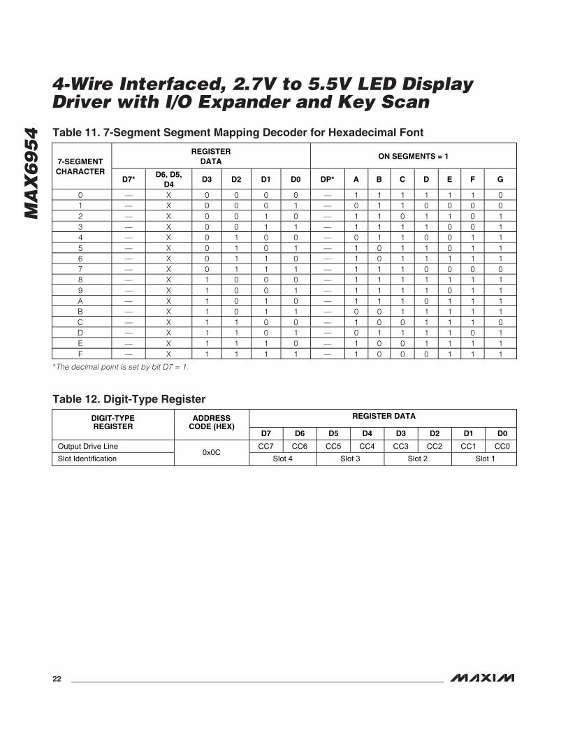
For 7-segment displays, the digit plane data registercan be used to address a character generator, whichcontains the data of a 16-character font containing thehexadecimal font. The decode mode register can beused to disable the character generator and allow thesegments to be controlled directly. Table 10 shows theone-to-one pairing of each data bit to the appropriatesegment line in the digit plane data registers. The hexa-decimal font is decoded according to Table 11.
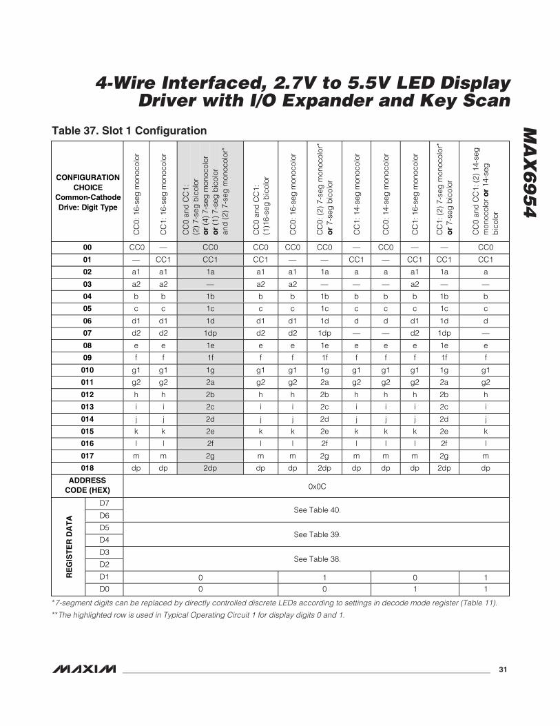
The digit-type register configures the display driver forvarious combinations of 14-segment digits, 16-segmentdigits, and/or pairs, or 7-segment digits. The function ofthis register is to select the appropriate font for eachdigit and route the output of the font to the appropriateMAX6954 driver output pins. The MAX6954 has fourdigit drive slots. A slot can be filled with various combi-nations of monocolor and bicolor 16-segment displays,14-segment displays, or two 7-segment displays. Eachpair of bits in the register corresponds to one of the four
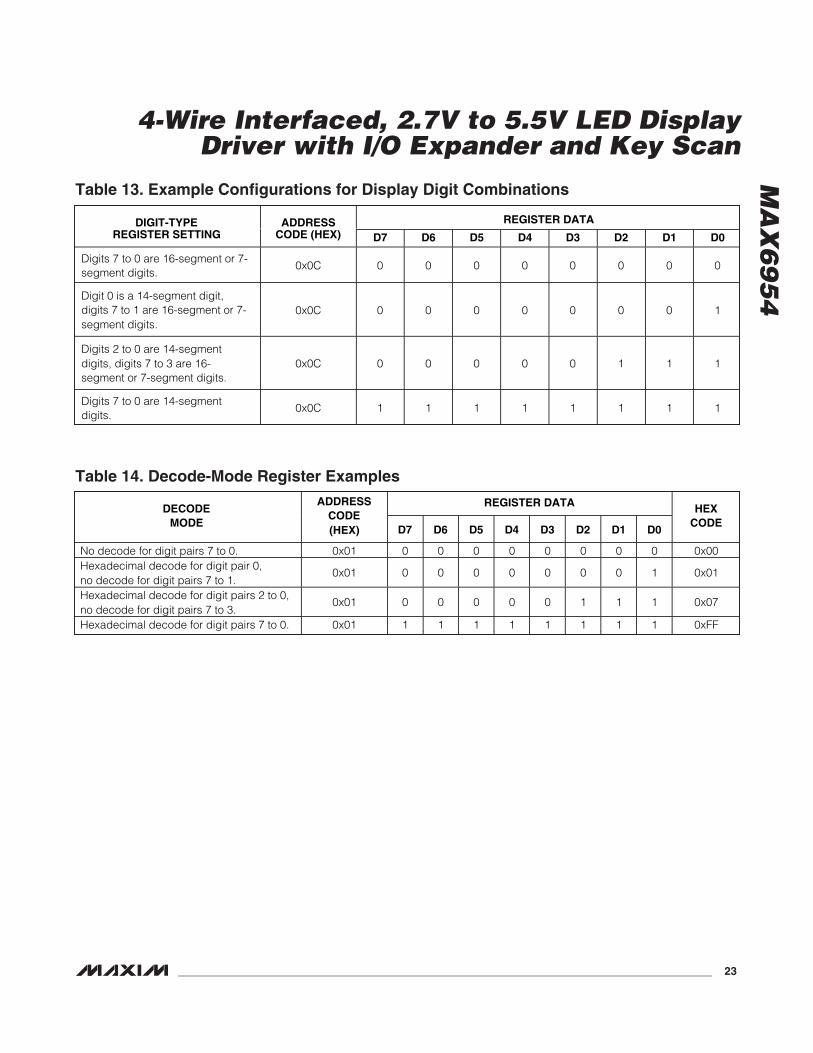
digit drive slots, as shown in Table 12. Each bit also cor-responds to one of the eight common-cathode digitdrive outputs, CC0 to CC7. When using bicolor digits,the anode connections for the two digits within a slot arealways the same. This means that a slot correctly drivestwo monocolor or one bicolor 14- or 16-segment digit.The digit type register can be written, but cannot beread. Examples of configuration settings required forsome display digit combinations are shown in Table 13.
7-Segment Decode-Mode RegisterIn 7-segment mode, the hexadecimal font can be dis-abled (Table 14). The decode-mode register selectsbetween hexadecimal code or direct control for each ofeight possible pairs of 7-segment digits. Each bit in theregister corresponds to one pair of digits. The digitpairs are {digit 0, digit 0a} through {digit 7, digit 7a}.Disabling decode mode allows direct control of the 16LEDs of a dual 7-segment display. Direct control modecan also be used to drive a matrix of 128 discreteLEDs.
CS
CLK
DIN D15 D14 D13 D12 D11 D10 D9 D8 D7 D6 D5 D4 D3 D2 D1 D0
DOUT D15 = 0
Figure 4. Transmission of 16 Bits to the MAX6954
CS
CLK
DIN BIT1
BIT2
N-9 N-8 N-7 N-6 N-5 N-4 N-3 N-2
DOUT N-15
N-15 N-14 N-13 N-12 N-11 N-10 N-1
N-31 N-30 N-29 N-28 N-27 N-26 N-25 N-24 N-23 N-22 N-21 N-20 N-19 N-18 N-17 N-16
N
Figure 5. Transmission of More than 16 Bits to the MAX6954
MA
X6
95
4
4-Wire Interfaced, 2.7V to 5.5V LED DisplayDriver with I/O Expander and Key Scan
______________________________________________________________________________________ 11
A logic high selects hexadecimal decoding, while alogic low bypasses the decoder. When direct control isselected, the data bits D7 to D0 correspond to the seg-ment lines of the MAX6954. Write x0010000 to blank allsegments in hexadecimal decode mode.
Display Blink ModeThe display blinking facility, when enabled, makes thedriver flip automatically between displaying the digitregister data in planes P0 and P1. If the digit registerdata for any digit is different in the two planes, then thatdigit appears to flip between two characters. To make acharacter appear to blink on or off, write the characterto one plane, and use the blank character (0x20) for theother plane. Once blinking has been configured, it con-tinues automatically without further intervention.
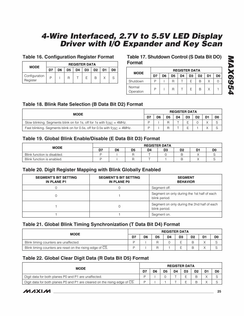
Blink SpeedThe blink speed is determined by the frequency of themultiplex clock, OSC, and by the setting of the BlinkRate Selection Bit B (Table 18) in the configuration reg-ister. The Blink Rate Selection Bit B sets either fast orslow blink speed for the whole display.
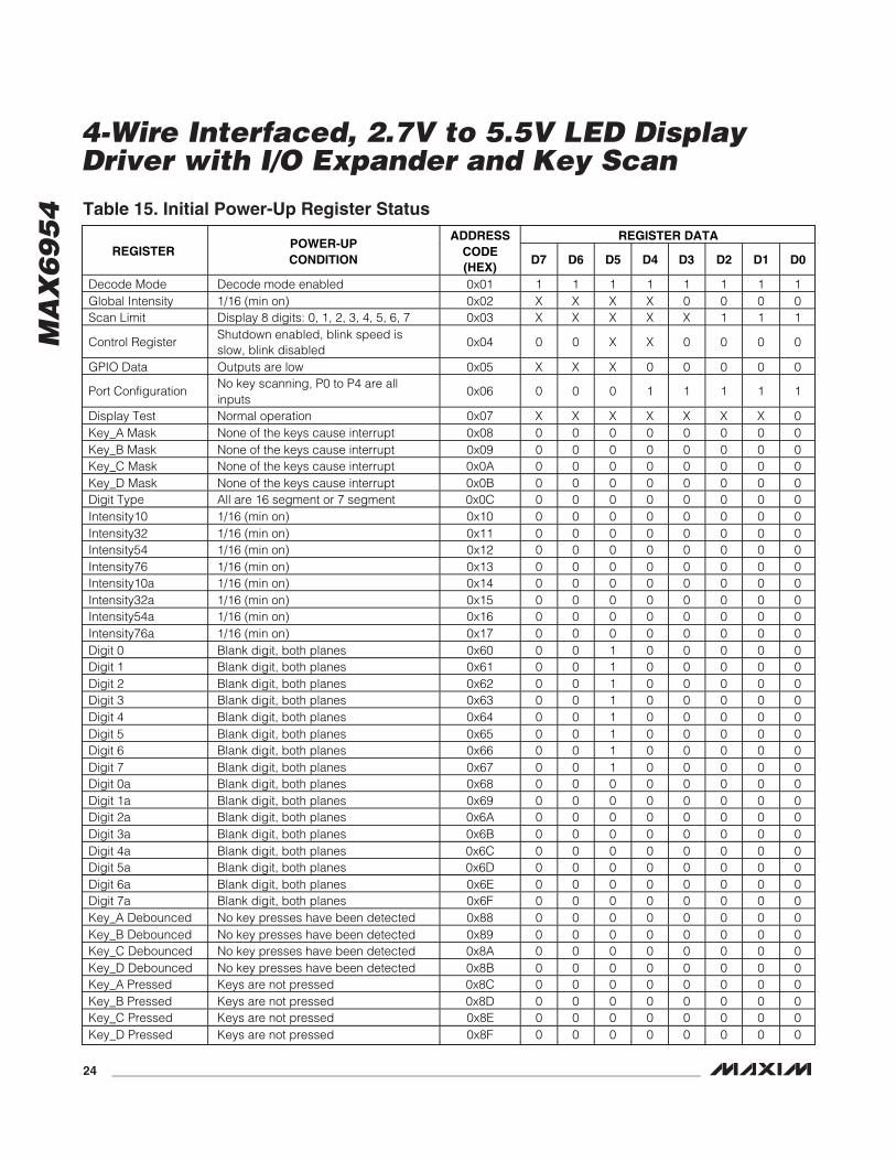
Initial Power-UpOn initial power-up, all control registers are reset, thedisplay is blanked, intensities are set to minimum, andshutdown is enabled (Table 15).
Configuration RegisterThe configuration register is used to enter and exit shut-down, select the blink rate, globally enable and disablethe blink function, globally clear the digit data, selectbetween global or digit-by-digit control of intensity, andreset the blink timing (Tables 16–19 and 21–24).
The configuration register contains 7 bits:
• S bit selects shutdown or normal operation(read/write).
• B bit selects the blink rate (read/write).
• E bit globally enables or disables the blink function(read/write).
• T bit resets the blink timing (data is not stored—tran-sient bit).
• R bit globally clears the digit data for both planes P0and P1 for ALL digits (data is not stored—transientbit).
• I bit selects between global or digit-by-digit controlof intensity (read/write).
• P bit returns the current phase of the blink timing(read only—a write to this bit is ignored).
Character Generator Font MappingThe font is composed of 104 characters in ROM. Thelower 7 bits of the 8-bit digit register represent the char-acter selection. The most significant bit, shown as x inthe ROM map of Tables 7 and 8, is 1 to light the DPsegment and zero to leave the DP segment unlit.
The character map follows the standard ASCII font for96 characters in the x0101000 through x1111111range. The first 16 characters of the 16-segment ROMmap cover 7-segment displays. These 16 charactersare numeric 0 to 9 and characters A to F (i.e., the hexa-decimal set).
Multiplex Clock and Blink TimingThe OSC pin can be fitted with capacitor CSET to GNDto use the internal RC multiplex oscillator, or driven byan external clock to set the multiplex clock frequencyand blink rate. The multiplex clock frequency deter-mines the frequency that the complete display is updat-ed. With OSC at 4MHz, each display digit is enabled for200µs.
The internal RC oscillator uses an external resistor,RSET, and an external capacitor, CSET, to set the oscil-lator frequency. The suggested values of RSET (56kΩ)and CSET (22pF) set the oscillator at 4MHz, whichmakes the blink frequency 0.5Hz or 1Hz.
The external clock is not required to have a 50:50 dutycycle, but the minimum time between transitions mustbe 50ns or greater and the maximum time betweentransitions must be 750ns.
The on-chip oscillator may be accurate enough forapplications using a single device. If an exact blink rateis required, use an external clock ranging between1MHz and 8MHz to drive OSC. The OSC inputs of multi-ple MAX6954s can be tied together to a common exter-nal clock to make the devices blink at the same rate.The relative blink phasing of multiple MAX6954s can besynchronized by setting the T bit in the control registerfor all the devices in quick succession. If the serial inter-faces of multiple MAX6954s are daisy-chained by con-necting the DOUT of one device to the DIN of the next,then synchronization is achieved automatically byupdating the configuration register for all devices simul-taneously. Figure 6 is the multiplex timing diagram.
OSC_OUT OutputThe OSC_OUT output is a buffered copy of either theinternal oscillator clock or the clock driven into the OSCpin if the external clock has been selected. The featureis useful if the internal oscillator is used, and the userwishes to synchronize other MAX6954s to the sameblink frequency. The oscillator is disabled while theMAX6954 is in shutdown.

MA
X6
95
4
4-Wire Interfaced, 2.7V to 5.5V LED DisplayDriver with I/O Expander and Key Scan
12 ______________________________________________________________________________________
Scan-Limit RegisterThe scan-limit register sets how many 14-segment dig-its or 16-segment digits or pairs of 7-segment digits aredisplayed, from 1 to 8. A bicolor digit is connected astwo monocolor digits. The scan register also limits thenumber of keys that can be scanned.
Since the number of scanned digits affects the displaybrightness, the scan-limit register should not be used toblank portions of the display (such as leading-zero sup-pression). Table 25 shows the scan-limit register format.
Intensity RegistersDigital control of display brightness is provided andcan be managed in one of two ways: globally or individ-ually. Global control adjusts all digits together.Individual control adjusts the digits separately.
The default method is global brightness control, whichis selected by clearing the global intensity bit (I data bitD6) in the configuration register. This brightness settingapplies to all display digits. The pulse-width modulatoris then set by the lower nibble of the global intensityregister, address 0x02. The modulator scales the aver-age segment current in 16 steps from a maximum of15/16 down to 1/16 of the peak current. The minimuminterdigit blanking time is set to 1/16 of a cycle. Whenusing bicolor digits, 256 color/brightness combinationsare available.
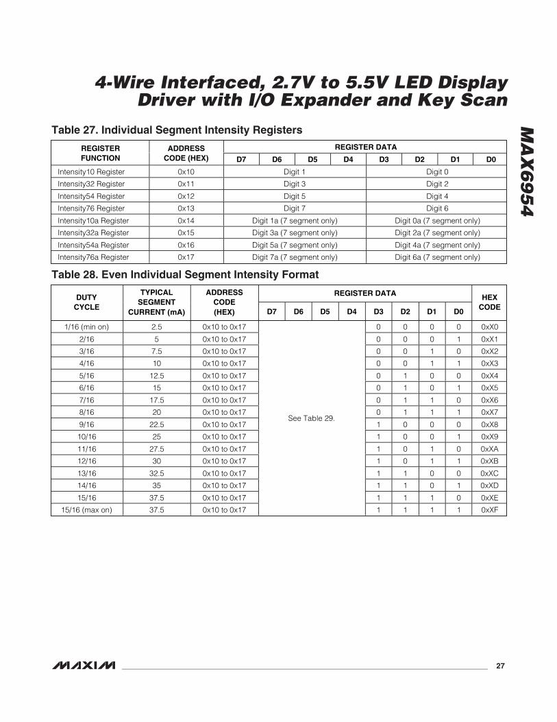
Individual brightness control is selected by setting theglobal intensity bit (I data bit D6) in the configurationregister. The pulse-width modulator is now no longerset by the lower nibble of the global intensity register,address 0x02, and the data is ignored. Individual digitalcontrol of display brightness is now provided by a sep-arate pulse-width modulator setting for each digit. Eachdigit is controlled by a nibble of one of the four intensityregisters: intensity10, intensity32, intensity54, and inten-sity76 for all display types, plus intensity10a, intensi-ty32a, intensity54a, and intensity76a for the extra eightdigits possible when 7-segment displays are used. Thedata from the relevant register is used for each digit asit is multiplexed. The modulator scales the averagesegment current in 16 steps in exactly the same way asglobal intensity adjustment.
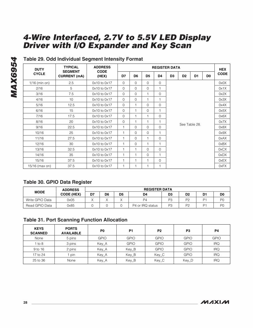
Table 26 shows the global intensity register format,Table 27 shows individual segment intensity registers,Table 28 is the even individual segment intensity for-mat, and Table 29 is the odd individual segment inten-sity format.
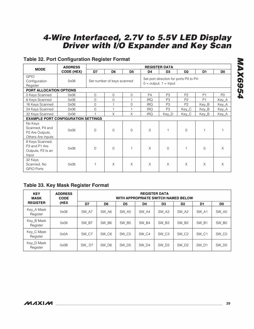
GPIO and Key ScanningThe MAX6954 feature five general-purpose input/output(GPIO) ports: P0 to P4. These ports can be individuallyenabled as logic inputs or open-drain logic outputs.The GPIO ports are not debounced when configured asinputs. The ports can be read and the outputs set usingthe 4-wire interface.
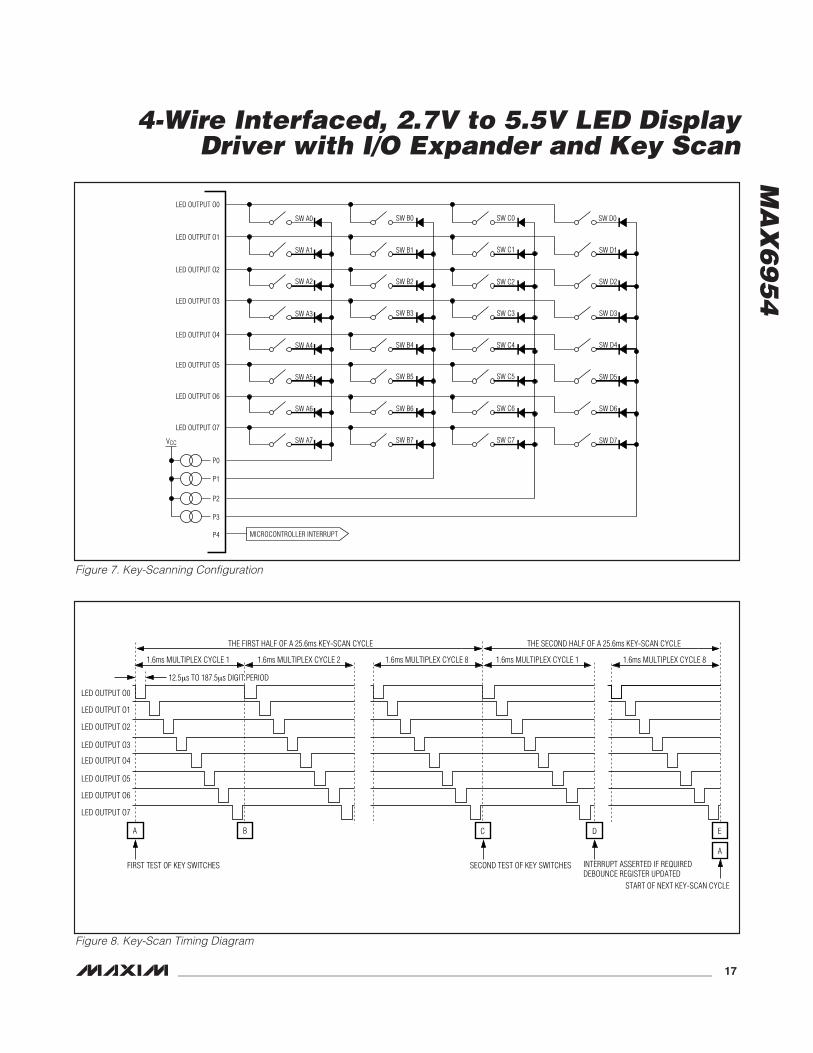
Some or all of the five ports can be configured to per-form key scanning of up to 32 keys. Ports P0 to P4 arerenamed Key_A, Key_B, Key_C, Key_D, and IRQ,respectively, when used for key scanning. The full key-scanning configuration is shown in Figure 7. Table 30 isthe GPIO data register.
One diode is required per key switch. These diodescan be common-anode dual diodes in SOT23 pack-ages, such as the BAW56. Sixteen diodes would berequired for the maximum 32-key configuration.
The MAX6954 can only scan the maximum 32 keys ifthe scan-limit register is set to scan the maximum eightdigits. If the MAX6954 is driving fewer digits, then amaximum of (4 x n) switches can be scanned, where nis the number of digits set in the scan-limit register. Forexample, if the MAX6954 is driving four 14-segmentdigits cathode drivers O0 to O3 are used. Only 16 keyscan be scanned in this configuration; the switchesshown connected to O4 through O7 are not read.
If the user wishes to scan fewer than 32 keys, thenfewer scan lines can be configured for key scanning.The unused Key_x ports are released back to their orig-inal GPIO functionality. If key scanning is enabled,regardless of the number of keys being scanned, P4 isalways configured as IRQ (Table 31).
The key-scanning circuit utilizes the LEDs’ common-cathode driver outputs as the key-scan drivers. O0 to07 go low for nominally 200µs (with OSC = 4MHz) inturn as the displays are multiplexed. By varying theoscillator frequency, the debounce time changes,though key scanning still functions. Key_x inputs haveinternal pullup resistors that allow the key condition tobe tested. The Key_x input is low during the appropri-ate digit multiplex period when the key is pressed. Thetiming diagram of Figure 8 shows the normal situationwhere all eight LED cathode drivers are used.
MA
X6
95
4
4-Wire Interfaced, 2.7V to 5.5V LED DisplayDriver with I/O Expander and Key Scan
______________________________________________________________________________________ 13
ADDRESS (COMMAND BYTE)REGISTER
D15 D14 D13 D12 D11 D10 D9 D8HEX CODE
No-Op R/W 0 0 0 0 0 0 0 0x00
Decode Mode R/W 0 0 0 0 0 0 1 0x01
Global Intensity R/W 0 0 0 0 0 1 0 0x02
Scan Limit R/W 0 0 0 0 0 1 1 0x03
Configuration R/W 0 0 0 0 1 0 0 0x04
GPIO Data R/W 0 0 0 0 1 0 1 0x05
Port Configuration R/W 0 0 0 0 1 1 0 0x06
Display Test R/W 0 0 0 0 1 1 1 0x07
Write KEY_A MaskRead KEY_A Debounce
R/W 0 0 0 1 0 0 0 0x08
Write KEY_B MaskRead KEY_B Debounce
R/W 0 0 0 1 0 0 1 0x09
Write KEY_C MaskRead KEY_C Debounce
R/W 0 0 0 1 0 1 0 0x0A
Write KEY_D MaskRead KEY_D Debounce
R/W 0 0 0 1 0 1 1 0x0B
Write Digit TypeRead KEY_A Pressed
R/W 0 0 0 1 1 0 0 0x0C
Read KEY_B Pressed* 1 0 0 0 1 1 0 1 0x0DRead KEY_C Pressed* 1 0 0 0 1 1 1 0 0x0ERead KEY_D Pressed* 1 0 0 0 1 1 1 1 0x0FIntensity 10 R/W 0 0 1 0 0 0 0 0x10Intensity 32 R/W 0 0 1 0 0 0 1 0x11Intensity 54 R/W 0 0 1 0 0 1 0 0x12Intensity 76 R/W 0 0 1 0 0 1 1 0x13Intensity 10a (7 Segment Only) R/W 0 0 1 0 1 0 0 0x14Intensity 32a (7 Segment Only) R/W 0 0 1 0 1 0 1 0x15Intensity 54a (7 Segment Only) R/W 0 0 1 0 1 1 0 0x16Intensity 76a (7 Segment Only) R/W 0 0 1 0 1 1 1 0x17Digit 0 Plane P0 R/W 0 1 0 0 0 0 0 0x20Digit 1 Plane P0 R/W 0 1 0 0 0 0 1 0x21Digit 2 Plane P0 R/W 0 1 0 0 0 1 0 0x22Digit 3 Plane P0 R/W 0 1 0 0 0 1 1 0x23Digit 4 Plane P0 R/W 0 1 0 0 1 0 0 0x24Digit 5 Plane P0 R/W 0 1 0 0 1 0 1 0x25Digit 6 Plane P0 R/W 0 1 0 0 1 1 0 0x26Digit 7 Plane P0 R/W 0 1 0 0 1 1 1 0x27Digit 0a Plane P0 (7 Segment Only) R/W 0 1 0 1 0 0 0 0x28Digit 1a Plane P0 (7 Segment Only) R/W 0 1 0 1 0 0 1 0x29Digit 2a Plane P0 (7 Segment Only) R/W 0 1 0 1 0 1 0 0x2ADigit 3a Plane P0 (7 Segment Only) R/W 0 1 0 1 0 1 1 0x2B
Table 6. Register Address Map
*Do NOT write to register.
MA
X6
95
4
4-Wire Interfaced, 2.7V to 5.5V LED DisplayDriver with I/O Expander and Key Scan
14 ______________________________________________________________________________________
ADDRESS (COMMAND BYTE)REGISTER
D15 D14 D13 D12 D11 D10 D9 D8HEX CODE
Digit 4a Plane P0 (7 Segment Only) R/W 0 1 0 1 1 0 0 0x2CDigit 5a Plane P0 (7 Segment Only) R/W 0 1 0 1 1 0 1 0x2DDigit 6a Plane P0 (7 Segment Only) R/W 0 1 0 1 1 1 0 0x2EDigit 7a Plane P0 (7 Segment Only) R/W 0 1 0 1 1 1 1 0x2FDigit 0 Plane P1 R/W 1 0 0 0 0 0 0 0x40Digit 1 Plane P1 R/W 1 0 0 0 0 0 1 0x41Digit 2 Plane P1 R/W 1 0 0 0 0 1 0 0x42Digit 3 Plane P1 R/W 1 0 0 0 0 1 1 0x43Digit 4 Plane P1 R/W 1 0 0 0 1 0 0 0x44Digit 5 Plane P1 R/W 1 0 0 0 1 0 1 0x45Digit 6 Plane P1 R/W 1 0 0 0 1 1 0 0x46Digit 7 Plane P1 R/W 1 0 0 0 1 1 1 0x47Digit 0a Plane P1 (7 Segment Only) R/W 1 0 0 1 0 0 0 0x48Digit 1a Plane P1 (7 Segment Only) R/W 1 0 0 1 0 0 1 0x49Digit 2a Plane P1 (7 Segment Only) R/W 1 0 0 1 0 1 0 0x4ADigit 3a Plane P1 (7 Segment Only) R/W 1 0 0 1 0 1 1 0x4BDigit 4a Plane P1 (7 Segment Only) R/W 1 0 0 1 1 0 0 0x4CDigit 5a Plane P1 (7 Segment Only) R/W 1 0 0 1 1 0 1 0x4DDigit 6a Plane P1 (7 Segment Only) R/W 1 0 0 1 1 1 0 0x4EDigit 7a Plane P1 (7 Segment Only) R/W 1 0 0 1 1 1 1 0x4F
Write Digit 0 Planes P0 and P1 with SameData, Reads as 0x00
R/W 1 1 0 0 0 0 0 0x60
Write Digit 1 Planes P0 and P1 with SameData, Reads as 0x00
R/W 1 1 0 0 0 0 1 0x61
Write Digit 2 Planes P0 and P1 with SameData, Reads as 0x00
R/W 1 1 0 0 0 1 0 0x62
Write Digit 3 Planes P0 and P1 with SameData, Reads as 0x00
R/W 1 1 0 0 0 1 1 0x63
Write Digit 4 Planes P0 and P1 with SameData, Reads as 0x00
R/W 1 1 0 0 1 0 0 0x64
Write Digit 5 Planes P0 and P1 with SameData, Reads as 0x00
R/W 1 1 0 0 1 0 1 0x65
Write Digit 6 Planes P0 and P1 with SameData, Reads as 0x00
R/W 1 1 0 0 1 1 0 0x66
Write Digit 7 Planes P0 and P1 with SameData, Reads as 0x00
R/W 1 1 0 0 1 1 1 0x67
Write Digit 0a Planes P0 and P1 with SameData (7 Segment Only), Reads as 0x00
R/W 1 1 0 1 0 0 0 0x68
Write Digit 1a Planes P0 and P1 with SameData (7 Segment Only), Reads as 0x00
R/W 1 1 0 1 0 0 1 0x69
Table 6. Register Address Map (continued)
The timing in Figure 8 loops over time, with 32 keysexperiencing a full key-scanning debounce over typi-cally 25.6ms. Four keys are sampled every 1.6ms, orevery multiplex cycle. If at least one key that was notpreviously pressed is found to have been pressed dur-ing both sampling periods, then that key press isdebounced, and an interrupt is issued. The key-scancircuit detects any combination of keys being pressedduring each debounce cycle (n-key rollover).
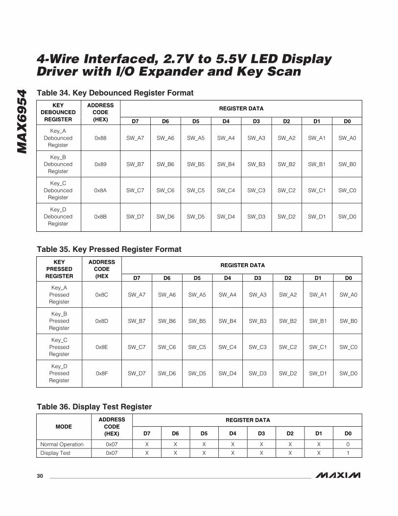
Port Configuration RegisterThe port configuration register selects how the five portpins are used. The port configuration register format isdescribed in Table 32.
Key Mask RegistersThe Key_A Mask, Key_B Mask, Key_C Mask, andKey_D Mask write-only registers (Table 33) configurethe key-scanning circuit to cause an interrupt only whenselected (masked) keys have been debounced. Eachbit in the register corresponds to one key switch. The bitis clear to disable interrupt for the switch, and set toenable interrupt. Keys are always scanned (if enabledthrough the port configuration register), regardless ofthe setting of these interrupt bits, and the key status isstored in the appropriate Key_x pressed register.
Key Debounced RegistersThe Key_A debounced, Key_B debounced, Key_Cdebounced, and Key_D debounced read-only registers(Table 34) show which keys have been detected asdebounced by the key-scanning circuit.
Each bit in the register corresponds to one key switch.The bit is set i f the switch has been correctlydebounced since the register was read last. Reading adebounced register clears that register (after the datahas been read) so that future keys pressed can beidentified. If the debounced registers are not read, thekey-scan data accumulates. However, as there is noFIFO in the MAX6954, the user is not able to determinekey order, or whether a key has been pressed morethan once, unless the debounced key status registersare read after each interrupt, and before the next key-scan cycle.
Reading any of the four debounced registers clears theIRQ output. If a key is pressed and held down, the key isreported as debounced (and IRQ issued) only once.The key must be detected as released by the key-scan-ning circuit, before it debounces again. If thedebounced registers are being read in response to theIRQ being asserted, then the user should generally readall four registers to ensure that all the keys that weredetected by the key-scanning circuit are discovered.
Key Pressed RegistersThe Key_A pressed, Key_B pressed, Key_C pressed,and Key_D pressed read-only registers (Table 35)show which keys have been detected as pressed bythe key-scanning circuit during the last test.
Each bit in the register corresponds to one key switch.The bit is set if the switch has been detected aspressed by the key-scanning circuit during the last test.
MA
X6
95
4
4-Wire Interfaced, 2.7V to 5.5V LED DisplayDriver with I/O Expander and Key Scan
______________________________________________________________________________________ 15
ADDRESS (COMMAND BYTE)REGISTER
D15 D14 D13 D12 D11 D10 D9 D8HEX CODE
Write Digit 2a Planes P0 and P1 with SameData (7 Segment Only), Reads as 0x00
R/W 1 1 0 1 0 1 0 0x6A
Write Digit 3a Planes P0 and P1 with SameData (7 Segment Only), Reads as 0x00
R/W 1 1 0 1 0 1 1 0x6B
Write Digit 4a Planes P0 and P1 with SameData (7 Segment Only), Reads as 0x00
R/W 1 1 0 1 1 0 0 0x6C
Write Digit 5a Planes P0 and P1 with SameData (7 Segment Only), Reads as 0x00
R/W 1 1 0 1 1 0 1 0x6D
Write Digit 6a Planes P0 and P1 with SameData (7 Segment Only), Reads as 0x00
R/W 1 1 0 1 1 1 0 0x6E
Write Digit 7a Planes P0 and P1 with SameData (7 Segment Only), Reads as 0x00
R/W 1 1 0 1 1 1 1 0x6F
Table 6. Register Address Map (continued)
Note: Unused register bits read as zero.

MA
X6
95
4
4-Wire Interfaced, 2.7V to 5.5V LED DisplayDriver with I/O Expander and Key Scan
16 ______________________________________________________________________________________
DIGIT 1
ONE COMPLETE 1.6ms MULTIPLEX CYCLE AROUND 8 DIGITS
DIGIT 0's 200μs MULTIPLEX TIMESLOT
DIGIT 0
200μs
DIGIT 2 DIGIT 3 DIGIT 4 DIGIT 5 DIGIT 6 DIGIT 7
START OFNEXT CYCLE
LOW
2/16TH
1/16TH
(MIN ON)
HIGH-Z
HIGH-Z
LOW
3/16TH HIGH-Z
LOW
4/16TH HIGH-Z
LOW
5/16TH HIGH-Z
LOW
6/16TH HIGH-Z
LOW
7/16TH HIGH-Z
LOW
8/16TH HIGH-Z
LOW
9/16TH HIGH-Z
LOW
10/16TH HIGH-Z
LOW
11/16TH HIGH-Z
LOW
12/16TH HIGH-Z
LOW
13/16TH HIGH-Z
LOW
14/16TH HIGH-Z
LOW
15/16TH HIGH-Z
LOW
15/16TH HIGH-Z(MAX ON)
HIGH-Z
HIGH-Z
CURRENT SOURCE ENABLED MINIMUM 12.5μs INTERDIGIT BLANKING INTERVAL
HIGH-Z
ANODE (LIT)
DIGIT 0 CATHODEDRIVER INTENSITYSETTINGS
ANODE (UNLIT)
Figure 6. Multiplex Timing Diagram (OSC = 4MHz)
MA
X6
95
4
4-Wire Interfaced, 2.7V to 5.5V LED DisplayDriver with I/O Expander and Key Scan
______________________________________________________________________________________ 17
LED OUTPUT O0
LED OUTPUT O1
LED OUTPUT O2
LED OUTPUT O3
LED OUTPUT O4
LED OUTPUT O5
LED OUTPUT O6
LED OUTPUT O7
12.5μs TO 187.5μs DIGIT PERIOD
1.6ms MULTIPLEX CYCLE 1 1.6ms MULTIPLEX CYCLE 2 1.6ms MULTIPLEX CYCLE 8
THE FIRST HALF OF A 25.6ms KEY-SCAN CYCLE
1.6ms MULTIPLEX CYCLE 8
THE SECOND HALF OF A 25.6ms KEY-SCAN CYCLE
1.6ms MULTIPLEX CYCLE 1
START OF NEXT KEY-SCAN CYCLE
FIRST TEST OF KEY SWITCHES SECOND TEST OF KEY SWITCHES INTERRUPT ASSERTED IF REQUIREDDEBOUNCE REGISTER UPDATED
CA
A
B D E
Figure 7. Key-Scanning Configuration
SW A0
SW A1
SW A2
SW A3
SW A4
SW A5
SW A6
SW A7
P0
VCC
LED OUTPUT O0
LED OUTPUT O1
LED OUTPUT O2
LED OUTPUT O3
LED OUTPUT O4
LED OUTPUT O5
LED OUTPUT O6
LED OUTPUT O7
P1
P2
P3
P4 MICROCONTROLLER INTERRUPT
SW B0
SW B1
SW B2
SW B3
SW B4
SW B5
SW B6
SW B7
SW C0
SW C1
SW C2
SW C3
SW C4
SW C5
SW C6
SW C7
SW D0
SW D1
SW D2
SW D3
SW D4
SW D5
SW D6
SW D7
Figure 8. Key-Scan Timing Diagram

MA
X6
95
4 The bit is cleared if the switch has not been detectedas pressed by the key-scanning circuit during the lasttest. Reading a pressed register does not clear thatregister or clear the IRQ output.
Display Test RegisterThe display test register (Table 36) operates in twomodes: normal and display test. Display test modeturns all LEDs on (including DPs) by overriding, but notaltering, all controls and digit registers (including theshutdown register), except for the digit-type registerand the GPIO configuration register. The duty cycle,while in display test mode, is 7/16 (see the ChoosingSupply Voltage to Minimize Power Dissipation section).
Selecting External Components RSET andCSET to Set Oscillator Frequency and
Peak Segment CurrentThe RC oscillator uses an external resistor, RSET, andan external capacitor, CSET, to set the frequency, fOSC.The allowed range of fOSC is 1MHz to 8MHz. RSET alsosets the peak segment current. The recommended val-ues of RSET and CSET set the oscillator to 4MHz, whichmakes the blink frequencies selectable between 0.5Hzand 1Hz. The recommended value of RSET also setsthe peak current to 40mA, which makes the segmentcurrent adjustable from 2.5mA to 37.5mA in 2.5mAsteps.
ISEG = KL / RSET mA
fOSC = KF / (RSET x CSET) MHz
where:
KL = 2240
KF = 5376
RSET = external resistor in kΩ
CSET = external capacitor in pF
CSTRAY = stray capacitance from OSC pin to GND inpF, typically 2pF
The recommended value of RSET is 56kΩ and the rec-ommended value of CSET is 22pF.
The recommended value or RSET is the minimumallowed value, since it sets the display driver to themaximum allowed peak segment current. RSET can beset to a higher value to set the segment current to alower peak value where desired. The user must alsoensure that the peak current specifications of the LEDsconnected to the driver are not exceeded.
The effective value of RSET includes not only the actualexternal capacitor used, but also the stray capacitancefrom OSC to GND. This capacitance is usually in the1pF to 5pF range, depending on the layout used.
Applications InformationDriving Bicolor LEDs
Bicolor digits group a red and a green die together foreach display element, so that the element can be lit redor green (or orange), depending on which die (or both)is lit. The MAX6954 allows each segment’s current tobe set individually from the 1/16th (minimum currentand LED intensity) to 15/16th (maximum current andLED intensity), as well as off (zero current). Thus, abicolor (red-green) segment pair can be set to 256color/intensity combinations.
Choosing Supply Voltage to MinimizePower Dissipation
The MAX6954 drives a peak current of 40mA into LEDswith a 2.2V forward-voltage drop when operated from asupply voltage of at least 3.0V. The minimum voltagedrop across the internal LED drivers is therefore (3.0V -2.2V) = 0.8V. If a higher supply voltage is used, the dri-ver absorbs a higher voltage, and the driver’s powerdissipation increases accordingly. However, if the LEDsused have a higher forward voltage drop than 2.2V, thesupply voltage must be raised accordingly to ensurethat the driver always has at least 0.8V of headroom.
The voltage drop across the drivers with a nominal 5Vsupply (5.0V - 2.2V) = 2.8V is nearly 3 times the dropacross the drivers with a nominal 3.3V supply (3.3V -2.2V) = 1.1V. In most systems, consumption is animportant design criterion, and the MAX6954 should beoperated from the system’s 3.3V nominal supply. Inother designs, the lowest supply voltage may be 5V.The issue now is to ensure the dissipation limit for theMAX6954 is not exceeded. This can be achieved byinserting a series resistor in the supply to the MAX6954,ensuring that the supply decoupling capacitors are stillon the MAX6954 side of the resistor. For example, con-sider the requirement that the minimum supply voltageto a MAX6954 must be 3.0V, and the input supplyrange is 5V ±5%. Maximum supply current is 35mA +(40mA x 17) = 715mA. Minimum input supply voltage is4.75V. Maximum series resistor value is (4.75V -3.0V)/0.715A = 2.44Ω. We choose 2.2Ω ±5%. Worst-case resistor dissipation is at maximum tolerancedresistance, i.e., (0.715A) 2 x (2.2Ω x 1.05) = 1.18W. Themaximum MAX6954 supply voltage is at maximuminput supply voltage and minimum toleranced resis-tance, i.e., 5.25V - (0.715A x 2.2Ω x 0.95) = 3.76V.
Low-Voltage OperationThe MAX6954 works over the 2.7V to 5.5V supplyrange. The minimum useful supply voltage is deter-mined by the forward voltage drop of the LEDs at the
4-Wire Interfaced, 2.7V to 5.5V LED DisplayDriver with I/O Expander and Key Scan
18 ______________________________________________________________________________________

peak current ISEG, plus the 0.8V headroom required bythe driver output stages. The MAX6954 correctly regu-lates ISEG with a supply voltage above this minimumvoltage. If the supply drops below this minimum volt-age, the driver output stages may brown out, and beunable to regulate the current correctly. As the supplyvoltage drops further, the LED segment drive currentbecomes effectively limited by the output driver's on-resistance, and the LED drive current drops. The char-acteristics of each individual LED in a display digit arewell matched, so the result is that the display intensitydims uniformly as supply voltage drops out of regula-tion and beyond.
Computing Power DissipationThe upper limit for power dissipation (PD) for theMAX6954 is determined from the following equation:
PD = (V+ x 35mA) + (V+ - VLED) (DUTY x ISEG x N)
where:
V+ = supply voltage
DUTY = duty cycle set by intensity register
N = number of segments driven (worst case is 17)
VLED = LED forward voltage at ISEG
ISEG = segment current set by RSET
PD = Power dissipation, in mW if currents are in mA
Dissipation example:
ISEG = 30mA, N = 17, DUTY = 15/16,VLED = 2.4V at 30mA, V+ = 3.6V
PD = 3.6V (35mA) + (3.6V - 2.4V)(15/16 x 30mA x 17) = 0.700W
Thus, for a 36-pin SSOP package (TJA = 1 / 0.0118 =+85°C/W from Operating Ratings), the maximumallowed ambient temperature TA is given by:
TJ(MAX) = TA + (PD x TJA) = +150°C = TA + (0.700 x +85°C/W)
So TA = +90.5°C. Thus, the part can be operated safelyat a maximum package temperature of +85°C.
Power SuppliesThe MAX6954 operates from a single 2.7V to 5.5Vpower supply. Bypass the power supply to GND with a0.1µF capacitor as close to the device as possible. Adda 47µF capacitor if the MAX6954 is not close to theboard's input bulk decoupling capacitor.
Terminating the Serial InterfaceThe MAX6954 uses fixed voltage thresholds of 0.6Vand 1.8V for the 4-wire interface inputs. These fixedthresholds allow the MAX6954 to be controlled by ahost operating from a lower supply voltage than theMAX6954; for example, 2.5V. The fixed thresholds alsoreduce the logic input noise margin when operating theMAX6954 from a higher supply voltage, such as 5V. Athigher supply voltages, it may be necessary to fit termi-nation components to the CLK, DIN, and CS inputs toavoid signal reflections that the MAX6954 couldrespond to as multiple transitions. Suitable terminationcomponents can be either a 33pF capacitor or 4.7kΩresistor fitted from each of the CLK, DIN, and CS inputsto GND.
MA
X6
95
4
4-Wire Interfaced, 2.7V to 5.5V LED DisplayDriver with I/O Expander and Key Scan
______________________________________________________________________________________ 19
MA
X6
95
4
4-Wire Interfaced, 2.7V to 5.5V LED DisplayDriver with I/O Expander and Key Scan
20 ______________________________________________________________________________________
x000 x010 x011 x100 x101 x110 x111x001
0000
0001
0010
0011
0100
0101
0110
0111
1000
1001
1010
1011
1100
1101
1110
1111
MSBLSB
Table 7. 16-Segment Display Font Map
x000 x010 x011 x100 x101 x110 x111x001
0000
0001
0010
0011
0100
0101
0110
0111
1000
1001
1010
1011
1100
1101
1110
1111
.
MSBLSB
Table 8. 14-Segment Display Font Map
MA
X6
95
4
4-Wire Interfaced, 2.7V to 5.5V LED DisplayDriver with I/O Expander and Key Scan
______________________________________________________________________________________ 21
REGISTER DATAMODE
ADDRESSCODE(HEX) D7 D6 D5 D4 D3 D2 D1 D0
14-segment or 16-segment mode, writing digit datato use font map data with decimal place unlit
0x20 to 0x2F0x40 to 0x4F0x60 to 0x6F
0 Bits D6 to D0 select font characters 0 to 127
14-segment or 16-segment mode, writing digit datato use font map data with decimal place lit
0x20 to 0x2F0x40 to 0x4F0x60 to 0x6F
1 Bits D6 to D0 select font characters 0 to 127
7-segment decode mode, DP unlit0x20 to 0x2F0x40 to 0x4F0x60 to 0x6F
0 0 0 0 D3 to D0
7-segment decode mode, DP lit0x20 to 0x2F0x40 to 0x4F0x60 to 0x6F
1 0 0 0 D3 to D0
7-segment no-decode mode0x20 to 0x2F0x40 to 0x4F0x60 to 0x6F
Direct control of 8 segments
Table 9. Digit Plane Data Register Format
REGISTER DATAMODE
ADDRESS CODE(HEX) D7 D6 D5 D4 D3 D2 D1 D0
Segment Line0x20 to 0x2F0x40 to 0x4F0x60 to 0x6F
dp a b c d e f g
Table 10. Segment Decoding for 7-Segment Displays
MA
X6
95
4
4-Wire Interfaced, 2.7V to 5.5V LED DisplayDriver with I/O Expander and Key Scan
22 ______________________________________________________________________________________
REGISTERDATA
ON SEGMENTS = 17-SEGMENTCHARACTER
D7*D6, D5,
D4D3 D2 D1 D0 DP* A B C D E F G
0 — X 0 0 0 0 — 1 1 1 1 1 1 01 — X 0 0 0 1 — 0 1 1 0 0 0 02 — X 0 0 1 0 — 1 1 0 1 1 0 13 — X 0 0 1 1 — 1 1 1 1 0 0 14 — X 0 1 0 0 — 0 1 1 0 0 1 15 — X 0 1 0 1 — 1 0 1 1 0 1 16 — X 0 1 1 0 — 1 0 1 1 1 1 17 — X 0 1 1 1 — 1 1 1 0 0 0 08 — X 1 0 0 0 — 1 1 1 1 1 1 19 — X 1 0 0 1 — 1 1 1 1 0 1 1A — X 1 0 1 0 — 1 1 1 0 1 1 1B — X 1 0 1 1 — 0 0 1 1 1 1 1C — X 1 1 0 0 — 1 0 0 1 1 1 0D — X 1 1 0 1 — 0 1 1 1 1 0 1E — X 1 1 1 0 — 1 0 0 1 1 1 1F — X 1 1 1 1 — 1 0 0 0 1 1 1
Table 11. 7-Segment Segment Mapping Decoder for Hexadecimal Font
REGISTER DATADIGIT-TYPEREGISTER
ADDRESSCODE (HEX)
D7 D6 D5 D4 D3 D2 D1 D0
Output Drive Line CC7 CC6 CC5 CC4 CC3 CC2 CC1 CC0
Slot Identification0x0C
Slot 4 Slot 3 Slot 2 Slot 1
Table 12. Digit-Type Register
*The decimal point is set by bit D7 = 1.
MA
X6
95
4
4-Wire Interfaced, 2.7V to 5.5V LED DisplayDriver with I/O Expander and Key Scan
______________________________________________________________________________________ 23
REGISTER DATADECODEMODE
ADDRESSCODE(HEX) D7 D6 D5 D4 D3 D2 D1 D0
HEXCODE
No decode for digit pairs 7 to 0. 0x01 0 0 0 0 0 0 0 0 0x00Hexadecimal decode for digit pair 0,no decode for digit pairs 7 to 1.
0x01 0 0 0 0 0 0 0 1 0x01
Hexadecimal decode for digit pairs 2 to 0,no decode for digit pairs 7 to 3.
0x01 0 0 0 0 0 1 1 1 0x07
Hexadecimal decode for digit pairs 7 to 0. 0x01 1 1 1 1 1 1 1 1 0xFF
Table 14. Decode-Mode Register Examples
REGISTER DATADIGIT-TYPEREGISTER SETTING
ADDRESSCODE (HEX) D7 D6 D5 D4 D3 D2 D1 D0
Digits 7 to 0 are 16-segment or 7-segment digits.
0x0C 0 0 0 0 0 0 0 0
Digit 0 is a 14-segment digit,digits 7 to 1 are 16-segment or 7-segment digits.
0x0C 0 0 0 0 0 0 0 1
Digits 2 to 0 are 14-segmentdigits, digits 7 to 3 are 16-segment or 7-segment digits.
0x0C 0 0 0 0 0 1 1 1
Digits 7 to 0 are 14-segmentdigits.
0x0C 1 1 1 1 1 1 1 1
Table 13. Example Configurations for Display Digit Combinations
MA
X6
95
4
4-Wire Interfaced, 2.7V to 5.5V LED DisplayDriver with I/O Expander and Key Scan
24 ______________________________________________________________________________________
REGISTER DATAREGISTER
POWER-UPCONDITION
ADDRESSCODE(HEX)
D7 D6 D5 D4 D3 D2 D1 D0
Decode Mode Decode mode enabled 0x01 1 1 1 1 1 1 1 1Global Intensity 1/16 (min on) 0x02 X X X X 0 0 0 0Scan Limit Display 8 digits: 0, 1, 2, 3, 4, 5, 6, 7 0x03 X X X X X 1 1 1
Control RegisterShutdown enabled, blink speed isslow, blink disabled
0x04 0 0 X X 0 0 0 0
GPIO Data Outputs are low 0x05 X X X 0 0 0 0 0
Port ConfigurationNo key scanning, P0 to P4 are allinputs
0x06 0 0 0 1 1 1 1 1
Display Test Normal operation 0x07 X X X X X X X 0Key_A Mask None of the keys cause interrupt 0x08 0 0 0 0 0 0 0 0Key_B Mask None of the keys cause interrupt 0x09 0 0 0 0 0 0 0 0Key_C Mask None of the keys cause interrupt 0x0A 0 0 0 0 0 0 0 0Key_D Mask None of the keys cause interrupt 0x0B 0 0 0 0 0 0 0 0Digit Type All are 16 segment or 7 segment 0x0C 0 0 0 0 0 0 0 0Intensity10 1/16 (min on) 0x10 0 0 0 0 0 0 0 0Intensity32 1/16 (min on) 0x11 0 0 0 0 0 0 0 0Intensity54 1/16 (min on) 0x12 0 0 0 0 0 0 0 0Intensity76 1/16 (min on) 0x13 0 0 0 0 0 0 0 0Intensity10a 1/16 (min on) 0x14 0 0 0 0 0 0 0 0Intensity32a 1/16 (min on) 0x15 0 0 0 0 0 0 0 0Intensity54a 1/16 (min on) 0x16 0 0 0 0 0 0 0 0Intensity76a 1/16 (min on) 0x17 0 0 0 0 0 0 0 0Digit 0 Blank digit, both planes 0x60 0 0 1 0 0 0 0 0Digit 1 Blank digit, both planes 0x61 0 0 1 0 0 0 0 0Digit 2 Blank digit, both planes 0x62 0 0 1 0 0 0 0 0Digit 3 Blank digit, both planes 0x63 0 0 1 0 0 0 0 0Digit 4 Blank digit, both planes 0x64 0 0 1 0 0 0 0 0Digit 5 Blank digit, both planes 0x65 0 0 1 0 0 0 0 0Digit 6 Blank digit, both planes 0x66 0 0 1 0 0 0 0 0Digit 7 Blank digit, both planes 0x67 0 0 1 0 0 0 0 0Digit 0a Blank digit, both planes 0x68 0 0 0 0 0 0 0 0Digit 1a Blank digit, both planes 0x69 0 0 0 0 0 0 0 0Digit 2a Blank digit, both planes 0x6A 0 0 0 0 0 0 0 0Digit 3a Blank digit, both planes 0x6B 0 0 0 0 0 0 0 0Digit 4a Blank digit, both planes 0x6C 0 0 0 0 0 0 0 0Digit 5a Blank digit, both planes 0x6D 0 0 0 0 0 0 0 0Digit 6a Blank digit, both planes 0x6E 0 0 0 0 0 0 0 0Digit 7a Blank digit, both planes 0x6F 0 0 0 0 0 0 0 0Key_A Debounced No key presses have been detected 0x88 0 0 0 0 0 0 0 0Key_B Debounced No key presses have been detected 0x89 0 0 0 0 0 0 0 0Key_C Debounced No key presses have been detected 0x8A 0 0 0 0 0 0 0 0Key_D Debounced No key presses have been detected 0x8B 0 0 0 0 0 0 0 0Key_A Pressed Keys are not pressed 0x8C 0 0 0 0 0 0 0 0Key_B Pressed Keys are not pressed 0x8D 0 0 0 0 0 0 0 0Key_C Pressed Keys are not pressed 0x8E 0 0 0 0 0 0 0 0Key_D Pressed Keys are not pressed 0x8F 0 0 0 0 0 0 0 0
Table 15. Initial Power-Up Register Status
MA
X6
95
4
4-Wire Interfaced, 2.7V to 5.5V LED DisplayDriver with I/O Expander and Key Scan
______________________________________________________________________________________ 25
REGISTER DATAMODE
D7 D6 D5 D4 D3 D2 D1 D0
ConfigurationRegister
P I R T E B X S
Table 16. Configuration Register Format
REGISTER DATAMODE
D7 D6 D5 D4 D3 D2 D1 D0
Shutdown P I R T E B X 0
NormalOperation
P I R T E B X 1
Table 17. Shutdown Control (S Data Bit DO)Format
REGISTER DATAMODE
D7 D6 D5 D4 D3 D2 D1 D0
Slow blinking. Segments blink on for 1s, off for 1s with fOSC = 4MHz. P I R T E 0 X S
Fast blinking. Segments blink on for 0.5s, off for 0.5s with fOSC = 4MHz. P I R T E 1 X S
Table 18. Blink Rate Selection (B Data Bit D2) Format
REGISTER DATAMODE
D7 D6 D5 D4 D3 D2 D1 D0Blink function is disabled. P I R T 0 B X SBlink function is enabled. P I R T 1 B X S
Table 19. Global Blink Enable/Disable (E Data Bit D3) Format
SEGMENT’S BIT SETTINGIN PLANE P1
SEGMENT’S BIT SETTINGIN PLANE P0
SEGMENTBEHAVIOR
0 0 Segment off.
0 1Segment on only during the 1st half of eachblink period.
1 0Segment on only during the 2nd half of eachblink period.
1 1 Segment on.
Table 20. Digit Register Mapping with Blink Globally Enabled
REGISTER DATAMODE
D7 D6 D5 D4 D3 D2 D1 D0
Blink timing counters are unaffected. P I R 0 E B X S
Blink timing counters are reset on the rising edge of CS. P I R 1 E B X S
Table 21. Global Blink Timing Synchronization (T Data Bit D4) Format
REGISTER DATAMODE
D7 D6 D5 D4 D3 D2 D1 D0
Digit data for both planes P0 and P1 are unaffected. P I 0 T E B X S
Digit data for both planes P0 and P1 are cleared on the rising edge of CS. P I 1 T E B X S
Table 22. Global Clear Digit Data (R Data Bit D5) Format

MA
X6
95
4
4-Wire Interfaced, 2.7V to 5.5V LED DisplayDriver with I/O Expander and Key Scan
26 ______________________________________________________________________________________
REGISTER DATAMODE
D7 D6 D5 D4 D3 D2 D1 D0
Intensity for all digits is controlled by one setting in the global intensity register. P 0 R T E B X S
Intensity for digits is controlled by the individual settings in the intensity10 andintensity76 registers.
P 1 R T E B X S
Table 23. Global Intensity (I Data Bit D6) Format
REGISTER DATAMODE
D7 D6 D5 D4 D3 D2 D1 D0P1 Blink Phase 0 I R T E B X SP0 Blink Phase 1 I R T E B X S
Table 24. Blink Phase Readback (P Data Bit D7) Format
REGISTER DATASCANLIMIT
ADDRESS CODE(HEX) D7 D6 D5 D4 D3 D2 D1 D0
HEXCODE
Display Digit 0 only 0x03 X X X X X 0 0 0 0x00
Display Digits 0 and 1 0x03 X X X X X 0 0 1 0x01
Display Digits 0 1 2 0x03 X X X X X 0 1 0 0x02
Display Digits 0 1 2 3 0x03 X X X X X 0 1 1 0x03
Display Digits 0 1 2 3 4 0x03 X X X X X 1 0 0 0x04
Display Digits 0 1 2 3 4 5 0x03 X X X X X 1 0 1 0x05
Display Digits 0 1 2 3 4 5 6 0x03 X X X X X 1 1 0 0x06
Display Digits 0 1 2 3 4 5 6 7 0x03 X X X X X 1 1 1 0x07
Table 25. Scan-Limit Register Format
REGISTER DATADUTYCYCLE
TYPICALSEGMENT
CURRENT (mA)
ADDRESSCODE (HEX)
D7 D6 D5 D4 D3 D2 D1 D0
HEXCODE
1/16 (min on) 2.5 0x02 X X X X 0 0 0 0 0xX0
2/16 5 0x02 X X X X 0 0 0 1 0xX1
3/16 7.5 0x02 X X X X 0 0 1 0 0xX2
4/16 10 0x02 X X X X 0 0 1 1 0xX3
5/16 12.5 0x02 X X X X 0 1 0 0 0xX4
6/16 15 0x02 X X X X 0 1 0 1 0xX5
7/16 17.5 0x02 X X X X 0 1 1 0 0xX6
8/16 20 0x02 X X X X 0 1 1 1 0xX7
9/16 22.5 0x02 X X X X 1 0 0 0 0xX8
10/16 25 0x02 X X X X 1 0 0 1 0xX9
11/16 27.5 0x02 X X X X 1 0 1 0 0xXA
12/16 30 0x02 X X X X 1 0 1 1 0xXB
13/16 32.5 0x02 X X X X 1 1 0 0 0xXC
14/16 35 0x02 X X X X 1 1 0 1 0xXD
15/16 37.5 0x02 X X X X 1 1 1 0 0xXE
15/16 (max on) 37.5 0x02 X X X X 1 1 1 1 0xXF
Table 26. Global Intensity Register Format
MA
X6
95
4
4-Wire Interfaced, 2.7V to 5.5V LED DisplayDriver with I/O Expander and Key Scan
______________________________________________________________________________________ 27
REGISTER DATAREGISTERFUNCTION
ADDRESSCODE (HEX) D7 D6 D5 D4 D3 D2 D1 D0
Intensity10 Register 0x10 Digit 1 Digit 0
Intensity32 Register 0x11 Digit 3 Digit 2
Intensity54 Register 0x12 Digit 5 Digit 4
Intensity76 Register 0x13 Digit 7 Digit 6
Intensity10a Register 0x14 Digit 1a (7 segment only) Digit 0a (7 segment only)
Intensity32a Register 0x15 Digit 3a (7 segment only) Digit 2a (7 segment only)
Intensity54a Register 0x16 Digit 5a (7 segment only) Digit 4a (7 segment only)
Intensity76a Register 0x17 Digit 7a (7 segment only) Digit 6a (7 segment only)
Table 27. Individual Segment Intensity Registers
REGISTER DATADUTYCYCLE
TYPICALSEGMENT
CURRENT (mA)
ADDRESSCODE(HEX) D7 D6 D5 D4 D3 D2 D1 D0
HEXCODE
1/16 (min on) 2.5 0x10 to 0x17 0 0 0 0 0xX0
2/16 5 0x10 to 0x17 0 0 0 1 0xX1
3/16 7.5 0x10 to 0x17 0 0 1 0 0xX2
4/16 10 0x10 to 0x17 0 0 1 1 0xX3
5/16 12.5 0x10 to 0x17 0 1 0 0 0xX4
6/16 15 0x10 to 0x17 0 1 0 1 0xX5
7/16 17.5 0x10 to 0x17 0 1 1 0 0xX6
8/16 20 0x10 to 0x17 0 1 1 1 0xX7
9/16 22.5 0x10 to 0x17 1 0 0 0 0xX8
10/16 25 0x10 to 0x17 1 0 0 1 0xX9
11/16 27.5 0x10 to 0x17 1 0 1 0 0xXA
12/16 30 0x10 to 0x17 1 0 1 1 0xXB
13/16 32.5 0x10 to 0x17 1 1 0 0 0xXC
14/16 35 0x10 to 0x17 1 1 0 1 0xXD
15/16 37.5 0x10 to 0x17 1 1 1 0 0xXE
15/16 (max on) 37.5 0x10 to 0x17
See Table 29.
1 1 1 1 0xXF
Table 28. Even Individual Segment Intensity Format
MA
X6
95
4
4-Wire Interfaced, 2.7V to 5.5V LED DisplayDriver with I/O Expander and Key Scan
28 ______________________________________________________________________________________
REGISTER DATADUTYCYCLE
TYPICALSEGMENT
CURRENT (mA)
ADDRESSCODE(HEX) D7 D6 D5 D4 D3 D2 D1 D0
HEXCODE
1/16 (min on) 2.5 0x10 to 0x17 0 0 0 0 0x0X
2/16 5 0x10 to 0x17 0 0 0 1 0x1X
3/16 7.5 0x10 to 0x17 0 0 1 0 0x2X
4/16 10 0x10 to 0x17 0 0 1 1 0x3X
5/16 12.5 0x10 to 0x17 0 1 0 0 0x4X
6/16 15 0x10 to 0x17 0 1 0 1 0x5X
7/16 17.5 0x10 to 0x17 0 1 1 0 0x6X
8/16 20 0x10 to 0x17 0 1 1 1 0x7X
9/16 22.5 0x10 to 0x17 1 0 0 0 0x8X
10/16 25 0x10 to 0x17 1 0 0 1 0x9X
11/16 27.5 0x10 to 0x17 1 0 1 0 0xAX
12/16 30 0x10 to 0x17 1 0 1 1 0xBX
13/16 32.5 0x10 to 0x17 1 1 0 0 0xCX
14/16 35 0x10 to 0x17 1 1 0 1 0xDX
15/16 37.5 0x10 to 0x17 1 1 1 0 0xEX
15/16 (max on) 37.5 0x10 to 0x17 1 1 1 1
See Table 28.
0xFX
Table 29. Odd Individual Segment Intensity Format
REGISTER DATAMODE
ADDRESSCODE (HEX) D7 D6 D5 D4 D3 D2 D1 D0
Write GPIO Data 0x05 X X X P4 P3 P2 P1 P0
Read GPIO Data 0x85 0 0 0 P4 or IRQ status P3 P2 P1 P0
Table 30. GPIO Data Register
KEYSSCANNED
PORTSAVAILABLE
P0 P1 P2 P3 P4
None 5 pins GPIO GPIO GPIO GPIO GPIO
1 to 8 3 pins Key_A GPIO GPIO GPIO IRQ
9 to 16 2 pins Key_A Key_B GPIO GPIO IRQ
17 to 24 1 pin Key_A Key_B Key_C GPIO IRQ
25 to 36 None Key_A Key_B Key_C Key_D IRQ
Table 31. Port Scanning Function Allocation
MA
X6
95
4
4-Wire Interfaced, 2.7V to 5.5V LED DisplayDriver with I/O Expander and Key Scan
______________________________________________________________________________________ 29
REGISTER DATAMODE
ADDRESSCODE (HEX) D7 D6 D5 D4 D3 D2 D1 D0
GPIOConfigurationRegister
0x06 Set number of keys scannedSet port direction for ports P0 to P4:0 = output, 1 = input
PORT ALLOCATION OPTIONS0 Keys Scanned 0x06 0 0 0 P4 P3 P2 P1 P08 Keys Scanned 0x06 0 0 1 IRQ P3 P2 P1 Key_A16 Keys Scanned 0x06 0 1 0 IRQ P3 P2 Key_B Key_A24 Keys Scanned 0x06 0 1 1 IRQ P3 Key_C Key_B Key_A32 Keys Scanned 0x06 1 X X IRQ Key_D Key_C Key_B Key_AEXAMPLE PORT CONFIGURATION SETTINGSNo KeysScanned, P4 andP2 Are Outputs,Others Are Inputs
0x06 0 0 0 0 1 0 1 1
8 Keys Scanned,P3 and P1 AreOutputs, P2 Is anInput
0x06 0 0 1 X 0 1 0 X
32 KeysScanned, NoGPIO Ports
0x06 1 X X X X X X X
Table 32. Port Configuration Register Format
REGISTER DATAWITH APPROPRIATE SWITCH NAMED BELOW
KEYMASK
REGISTER
ADDRESSCODE(HEX D7 D6 D5 D4 D3 D2 D1 D0
Key_A MaskRegister
0x08 SW_A7 SW_A6 SW_A5 SW_A4 SW_A3 SW_A2 SW_A1 SW_A0
Key_B MaskRegister
0x09 SW_B7 SW_B6 SW_B5 SW_B4 SW_B3 SW_B2 SW_B1 SW_B0
Key_C MaskRegister
0x0A SW_C7 SW_C6 SW_C5 SW_C4 SW_C3 SW_C2 SW_C1 SW_C0
Key_D MaskRegister
0x0B SW_ D7 SW_D6 SW_D5 SW_D4 SW_D3 SW_D2 SW_D1 SW_D0
Table 33. Key Mask Register Format
MA
X6
95
4
4-Wire Interfaced, 2.7V to 5.5V LED DisplayDriver with I/O Expander and Key Scan
30 ______________________________________________________________________________________
REGISTER DATAKEYDEBOUNCED
REGISTER
ADDRESSCODE(HEX) D7 D6 D5 D4 D3 D2 D1 D0
Key_ADebounced
Register0x88 SW_A7 SW_A6 SW_A5 SW_A4 SW_A3 SW_A2 SW_A1 SW_A0
Key_BDebounced
Register0x89 SW_B7 SW_B6 SW_B5 SW_B4 SW_B3 SW_B2 SW_B1 SW_B0
Key_CDebounced
Register0x8A SW_C7 SW_C6 SW_C5 SW_C4 SW_C3 SW_C2 SW_C1 SW_C0
Key_DDebounced
Register0x8B SW_D7 SW_D6 SW_D5 SW_D4 SW_D3 SW_D2 SW_D1 SW_D0
Table 34. Key Debounced Register Format
REGISTER DATAKEYPRESSEDREGISTER
ADDRESSCODE(HEX D7 D6 D5 D4 D3 D2 D1 D0
Key_APressedRegister
0x8C SW_A7 SW_A6 SW_A5 SW_A4 SW_A3 SW_A2 SW_A1 SW_A0
Key_BPressedRegister
0x8D SW_B7 SW_B6 SW_B5 SW_B4 SW_B3 SW_B2 SW_B1 SW_B0
Key_CPressedRegister
0x8E SW_C7 SW_C6 SW_C5 SW_C4 SW_C3 SW_C2 SW_C1 SW_C0
Key_DPressedRegister
0x8F SW_D7 SW_D6 SW_D5 SW_D4 SW_D3 SW_D2 SW_D1 SW_D0
Table 35. Key Pressed Register Format
REGISTER DATAMODE
ADDRESSCODE(HEX) D7 D6 D5 D4 D3 D2 D1 D0
Normal Operation 0x07 X X X X X X X 0
Display Test 0x07 X X X X X X X 1
Table 36. Display Test Register
MA
X6
95
4
4-Wire Interfaced, 2.7V to 5.5V LED DisplayDriver with I/O Expander and Key Scan
______________________________________________________________________________________ 31
C O N F I G U R A T IO N C H O IC E
C o m m o n - C a t h o d e D r i v e : D ig it Ty p e
CC
0: 1
6-se
g m
onoc
olor
CC
1: 1
6-se
g m
onoc
olor
CC
0 an
d C
C1:
(2)
7-se
g b
icol
oro
r (4
) 7-
seg
mon
ocol
oro
r (1
) 7-
seg
bic
olor
and
(2)
7-s
eg m
onoc
olor
*
CC
0 an
d C
C1:
(1)1
6-se
g b
icol
or
CC
0: 1
6-se
g m
onoc
olor
CC
0: (
2) 7
-seg
mon
ocol
or*
or
7-se
g b
icol
or
CC
1: 1
4-se
g m
onoc
olor
CC
0: 1
4-se
g m
onoc
olor
CC
1: 1
6-se
g m
onoc
olor
CC
1: (
2) 7
-seg
mon
ocol
or*
or
7-se
g b
icol
or
CC
0 an
d C
C1:
(2)
14-
seg
mon
ocol
or o
r 14
-seg
bic
olor
00 CC0 — CC0 CC0 CC0 CC0 — CC0 — — CC0
01 — CC1 CC1 CC1 — — CC1 — CC1 CC1 CC1
02 a1 a1 1a a1 a1 1a a a a1 1a a
03 a2 a2 — a2 a2 — — — a2 — —
04 b b 1b b b 1b b b b 1b b
05 c c 1c c c 1c c c c 1c c
06 d1 d1 1d d1 d1 1d d d d1 1d d
07 d2 d2 1dp d2 d2 1dp — — d2 1dp —
08 e e 1e e e 1e e e e 1e e
09 f f 1f f f 1f f f f 1f f
010 g1 g1 1g g1 g1 1g g1 g1 g1 1g g1
011 g2 g2 2a g2 g2 2a g2 g2 g2 2a g2
012 h h 2b h h 2b h h h 2b h
013 i i 2c i i 2c i i i 2c i
014 j j 2d j j 2d j j j 2d j
015 k k 2e k k 2e k k k 2e k
016 l l 2f l l 2f l l l 2f l
017 m m 2g m m 2g m m m 2g m
018 dp dp 2dp dp dp 2dp dp dp dp 2dp dp
ADDRESSCODE (HEX) 0x0C
D7
D6See Table 40.
D5
D4See Table 39.
D3
D2See Table 38.
D1 0 1 0 1RE
GIS
TE
R D
AT
A
D0 0 0 1 1
Table 37. Slot 1 Configuration
*7-segment digits can be replaced by directly controlled discrete LEDs according to settings in decode mode register (Table 11).
**The highlighted row is used in Typical Operating Circuit 1 for display digits 0 and 1.
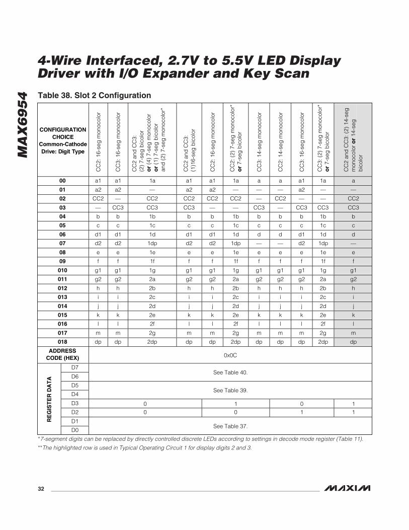
MA
X6
95
4
4-Wire Interfaced, 2.7V to 5.5V LED DisplayDriver with I/O Expander and Key Scan
32 ______________________________________________________________________________________
*7-segment digits can be replaced by directly controlled discrete LEDs according to settings in decode mode register (Table 11).
**The highlighted row is used in Typical Operating Circuit 1 for display digits 2 and 3.
C O N F I G U R A T IO N C H O IC E
C o m m o n - C a t h o d e D r i v e : D ig it Ty p e
CC
2: 1
6-se
g m
onoc
olor
CC
3: 1
6-se
g m
onoc
olor
CC
2 an
d C
C3:
(2)
7-se
g b
icol
oro
r (4
) 7-
seg
mon
ocol
oro
r (1
) 7-
seg
bic
olor
and
(2)
7-s
eg m
onoc
olor
*
CC
2 an
d C
C3:
(1)1
6-se
g b
icol
or
CC
2: 1
6-se
g m
onoc
olor
CC
2: (
2) 7
-seg
mon
ocol
or*
or
7-se
g b
icol
or
CC
3: 1
4-se
g m
onoc
olor
CC
2: 1
4-se
g m
onoc
olor
CC
3: 1
6-se
g m
onoc
olor
CC
3: (
2) 7
-seg
mon
ocol
or*
or
7-se
g b
icol
or
CC
2 an
d C
C3:
(2)
14-
seg
mon
ocol
or o
r 14
-seg
bic
olor
00 a1 a1 1a a1 a1 1a a a a1 1a a
01 a2 a2 — a2 a2 — — — a2 — —
02 CC2 — CC2 CC2 CC2 CC2 — CC2 — — CC2
03 — CC3 CC3 CC3 — — CC3 — CC3 CC3 CC3
04 b b 1b b b 1b b b b 1b b
05 c c 1c c c 1c c c c 1c c
06 d1 d1 1d d1 d1 1d d d d1 1d d
07 d2 d2 1dp d2 d2 1dp — — d2 1dp —
08 e e 1e e e 1e e e e 1e e
09 f f 1f f f 1f f f f 1f f
010 g1 g1 1g g1 g1 1g g1 g1 g1 1g g1
011 g2 g2 2a g2 g2 2a g2 g2 g2 2a g2
012 h h 2b h h 2b h h h 2b h
013 i i 2c i i 2c i i i 2c i
014 j j 2d j j 2d j j j 2d j
015 k k 2e k k 2e k k k 2e k
016 l l 2f l l 2f l l l 2f l
017 m m 2g m m 2g m m m 2g m
018 dp dp 2dp dp dp 2dp dp dp dp 2dp dp
ADDRESSCODE (HEX) 0x0C
D7
D6See Table 40.
D5
D4See Table 39.
D3 0 1 0 1D2 0 0 1 1
D1RE
GIS
TE
R D
AT
A
D0See Table 37.
Table 38. Slot 2 Configuration
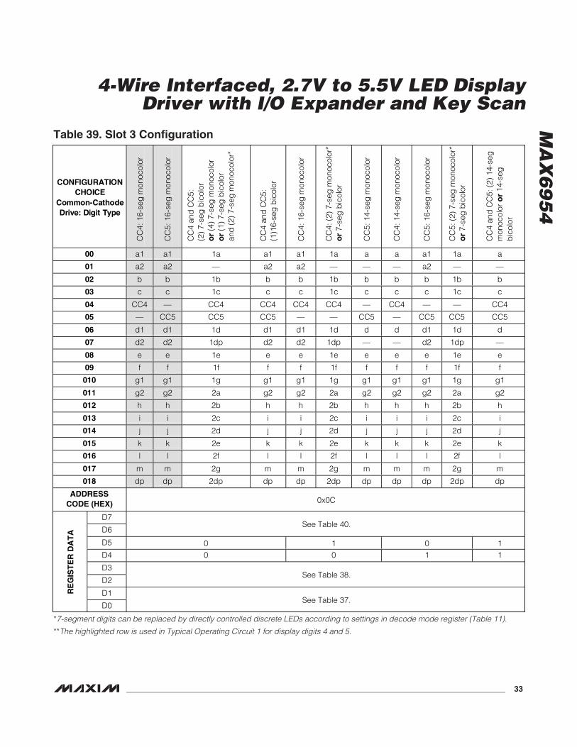
MA
X6
95
4
C O N F I G U R A T IO N C H O IC E
C o m m o n - C a t h o d e D r i v e : D ig it Ty p e
CC
4: 1
6-se
g m
onoc
olor
CC
5: 1
6-se
g m
onoc
olor
CC
4 an
d C
C5:
(2)
7-se
g b
icol
oro
r (4
) 7-
seg
mon
ocol
oro
r (1
) 7-
seg
bic
olor
and
(2)
7-s
eg m
onoc
olor
*
CC
4 an
d C
C5:
(1)1
6-se
g b
icol
or
CC
4: 1
6-se
g m
onoc
olor
CC
4: (
2) 7
-seg
mon
ocol
or*
or
7-se
g b
icol
or
CC
5: 1
4-se
g m
onoc
olor
CC
4: 1
4-se
g m
onoc
olor
CC
5: 1
6-se
g m
onoc
olor
CC
5: (
2) 7
-seg
mon
ocol
or*
or
7-se
g b
icol
or
CC
4 an
d C
C5:
(2)
14-
seg
mon
ocol
or o
r 14
-seg
bic
olor
00 a1 a1 1a a1 a1 1a a a a1 1a a
01 a2 a2 — a2 a2 — — — a2 — —
02 b b 1b b b 1b b b b 1b b
03 c c 1c c c 1c c c c 1c c
04 CC4 — CC4 CC4 CC4 CC4 — CC4 — — CC4
05 — CC5 CC5 CC5 — — CC5 — CC5 CC5 CC5
06 d1 d1 1d d1 d1 1d d d d1 1d d
07 d2 d2 1dp d2 d2 1dp — — d2 1dp —
08 e e 1e e e 1e e e e 1e e
09 f f 1f f f 1f f f f 1f f
010 g1 g1 1g g1 g1 1g g1 g1 g1 1g g1
011 g2 g2 2a g2 g2 2a g2 g2 g2 2a g2
012 h h 2b h h 2b h h h 2b h
013 i i 2c i i 2c i i i 2c i
014 j j 2d j j 2d j j j 2d j
015 k k 2e k k 2e k k k 2e k
016 l l 2f l l 2f l l l 2f l
017 m m 2g m m 2g m m m 2g m
018 dp dp 2dp dp dp 2dp dp dp dp 2dp dp
ADDRESSCODE (HEX) 0x0C
D7
D6See Table 40.
D5 0 1 0 1D4 0 0 1 1
D3
D2See Table 38.
D1RE
GIS
TE
R D
AT
A
D0See Table 37.
Table 39. Slot 3 Configuration
4-Wire Interfaced, 2.7V to 5.5V LED DisplayDriver with I/O Expander and Key Scan
______________________________________________________________________________________ 33
*7-segment digits can be replaced by directly controlled discrete LEDs according to settings in decode mode register (Table 11).
**The highlighted row is used in Typical Operating Circuit 1 for display digits 4 and 5.

MA
X6
95
4
4-Wire Interfaced, 2.7V to 5.5V LED DisplayDriver with I/O Expander and Key Scan
34 ______________________________________________________________________________________
*7-segment digits can be replaced by directly controlled discrete LEDs according to settings in the decode mode register (Table 11).
**The highlighted row is used in Typical Operating Circuit 1 for display digits 6 and 7.
C O N F I G U R A T IO N C H O IC E
C o m m o n - C a t h o d e D r i v e : D ig it Ty p e
CC
6: 1
6-se
g m
onoc
olor
CC
7: 1
6-se
g m
onoc
olor
CC
6 an
d C
C7:
(2)
7-se
g b
icol
oro
r (4
) 7-
seg
mon
ocol
oro
r (1
) 7-
seg
bic
olor
and
(2)
7-s
eg m
onoc
olor
*
CC
6 an
d C
C7:
(1)1
6-se
g b
icol
or
CC
6: 1
6-se
g m
onoc
olor
CC
6: (
2) 7
-seg
mon
ocol
or*
or
7-se
g b
icol
or
CC
7: 1
4-se
g m
onoc
olor
CC
6: 1
4-se
g m
onoc
olor
CC
7: 1
6-se
g m
onoc
olor
CC
7: (
2) 7
-seg
mon
ocol
or*
or
7-se
g b
icol
or
CC
6 an
d C
C7:
(2)
14-
seg
mon
ocol
or o
r 14
-seg
bic
olor
00 a1 a1 1a a1 a1 1a a a a1 1a a
01 a2 a2 — a2 a2 — — — a2 — —
02 b b 1b b b 1b b b b 1b b
03 c c 1c c c 1c c c c 1c c
04 d1 d1 1d d1 d1 1d d d d1 1d d
05 d2 d2 1dp d2 d2 1dp — — d2 1dp —
06 CC6 — CC6 CC6 CC6 CC6 — CC6 — — CC6
07 — CC7 CC7 CC7 — — CC7 — CC7 CC7 CC7
08 e e 1e e e 1e e e e 1e e
09 f f 1f f f 1f f f f 1f f
010 g1 g1 1g g1 g1 1g g1 g1 g1 1g g1
011 g2 g2 2a g2 g2 2a g2 g2 g2 2a g2
012 h h 2b h h 2b h h h 2b h
013 i i 2c i i 2c i i i 2c i
014 j j 2d j j 2d j j j 2d j
015 k k 2e k k 2e k k k 2e k
016 l l 2f l l 2f l l l 2f l
017 m m 2g m m 2g m m m 2g m
018 dp dp 2dp dp dp 2dp dp dp dp 2dp dp
ADDRESSCODE (HEX) 0x0C
D7 0 1 0 1
D6 0 0 1 1
D5
D4See Table 39.
D3
D2See Table 38.
D1RE
GIS
TE
R D
AT
A
D0See Table 37.
Table 40. Slot 4 Configuration
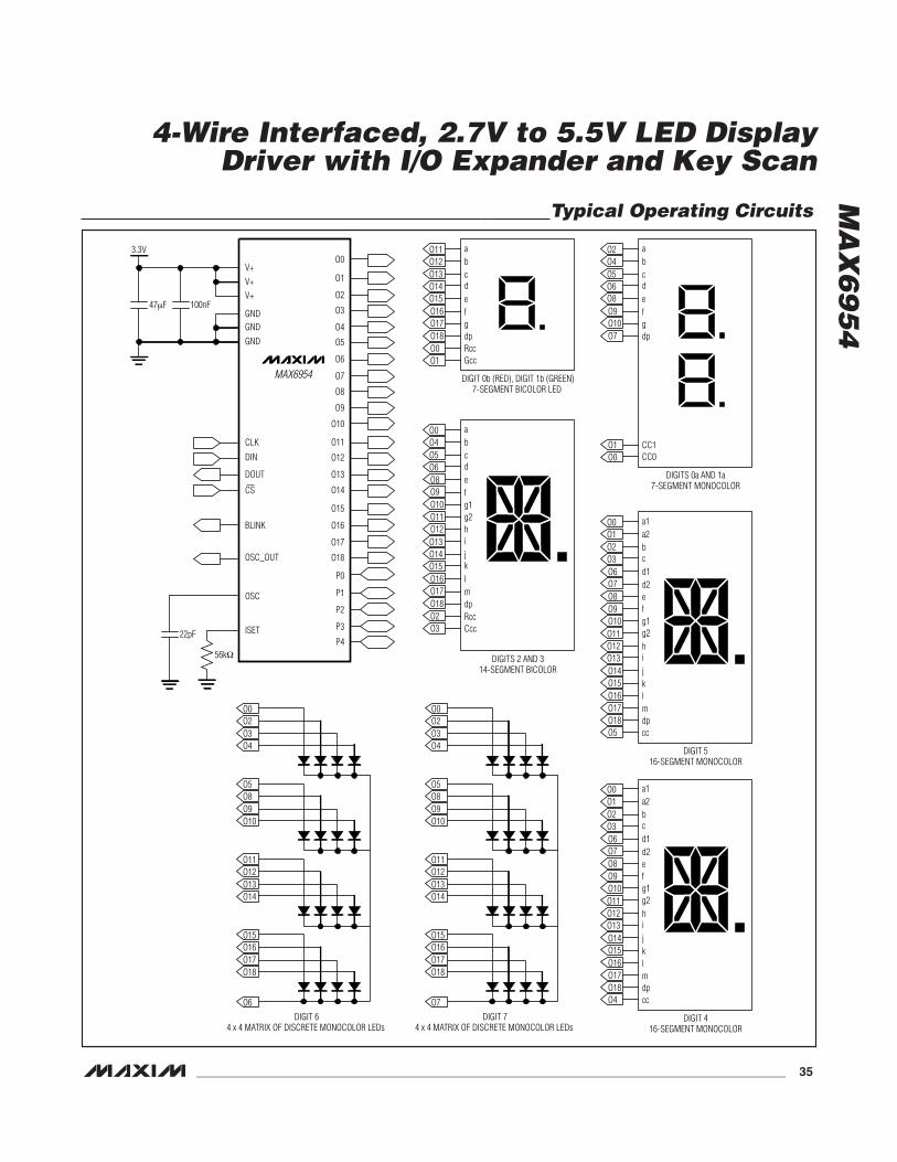
MA
X6
95
4f
a
Rccdpg
Gcc
bc
ed
DIGIT 0b (RED), DIGIT 1b (GREEN)7-SEGMENT BICOLOR LED
O16O17O18O0O1
O11O12O13O14
O0O2O3O4
O15
f
a
hg2g1
i
bc
ed
DIGITS 2 AND 314-SEGMENT BICOLOR
DIGIT 64 x 4 MATRIX OF DISCRETE MONOCOLOR LEDs
O8O9O10O11O12
O0O4O5O6
m
Rccdp
Ccc
j
lk
O16O17O18O2O3
O13O14O15
f
a
CC1
dpg
CC0
bc
ed
DIGITS 0a AND 1a7-SEGMENT MONOCOLOR
O9O10O7
O1O0
O2O4O5O6O8
d2
a1
g1fe
g2
a2b
d1c
DIGIT 516-SEGMENT MONOCOLOR
O6O7O8O9O10
O0O1O2O3
k
ml
dp
h
ji
O14O15O16O17O18
ccO5
O11O12O13
d2
a1
g1fe
g2
a2b
d1c
DIGIT 416-SEGMENT MONOCOLOR
O6O7O8O9O10
O0O1O2O3
k
ml
dp
h
ji
O14O15O16O17O18
ccO4
O11O12O13
3.3V
100nF47μF
O0
O1
O2
O3
O4
O5
O6
O7
O8
O9
O10
O11
O12
O13
O14
O15
O16
O17
O18
P0
P1
P2
P3
P4ISET
56kΩ
OSC_OUT
OSC
V+V+
GND
GND
DOUT
V+
GND
DIN
CLK
CS
BLINK
O5O8O9O10
O11O12O13O14
O15O16O17O18
O6
22pF
O0O2O3O4
DIGIT 74 x 4 MATRIX OF DISCRETE MONOCOLOR LEDs
O5O8O9O10
O11O12O13O14
O15O16O17O18
O7
MAX6954
Typical Operating Circuits
4-Wire Interfaced, 2.7V to 5.5V LED DisplayDriver with I/O Expander and Key Scan
______________________________________________________________________________________ 35
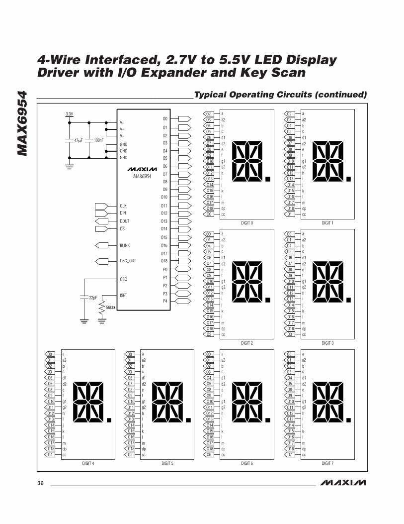
MA
X6
95
4
4-Wire Interfaced, 2.7V to 5.5V LED DisplayDriver with I/O Expander and Key Scan
36 ______________________________________________________________________________________
d2
a
g1fe
g2
a2b
d1c
DIGIT 0
O6O7O8O9O10
O2O3O4O5
k
ml
dp
h
ji
O14O15O16O17O18
ccO0
O11O12O13
d2
a
g1fe
g2
a2b
d1c
DIGIT 2
O6O7O8O9O10
O0O1O4O5
k
ml
dp
h
ji
O14O15O16O17O18
ccO2
O11O12O13
3.3V
100nF47μF
O0
O1
O2
O3
O4
O5
O6
O7
O8
O9
O10
O11
O12
O13
O14
O15
O16
O17
O18
P0
P1
P2
P3
P4ISET
OSC_OUT
OSC
V+V+
GND
GND
DOUT
V+
GND
DIN
CLK
CS
BLINK
d2
a
g1fe
g2
a2b
d1c
DIGIT 1
O6O7O8O9O10
O2O3O4O5
k
ml
dp
h
ji
O14O15O16O17O18
ccO1
O11O12O13
d2
a
g1fe
g2
a2b
d1c
DIGIT 3
O6O7O8O9O10
O0O1O4O5
k
ml
dp
h
ji
O14O15O16O17O18
ccO3
O11O12O13
d2
a
g1fe
g2
a2b
d1c
DIGIT 6
O4O5O8O9O10
O0O1O2O3
k
ml
dp
h
ji
O14O15O16O17O18
ccO6
O11O12O13
d2
a
g1fe
g2
a2b
d1c
DIGIT 7
O4O5O8O9O10
O0O1O2O3
k
ml
dp
h
ji
O14O15O16O17O18
ccO7
O11O12O13
d2
a
g1fe
g2
a2b
d1c
DIGIT 4
O6O6O8O9O10
O0O1O2O3
k
ml
dp
h
ji
O14O15O16O17O18
ccO4
O11O12O13
d2
a
g1fe
g2
a2b
d1c
DIGIT 5
O6O7O8O9O10
O0O1O2O3
k
ml
dp
h
ji
O14O15O16O17O18
ccO5
O11O12O13
MAX6954
56kΩ
22pF
Typical Operating Circuits (continued)

MA
X6
95
4
4-Wire Interfaced, 2.7V to 5.5V LED DisplayDriver with I/O Expander and Key Scan
______________________________________________________________________________________ 37
40
N.C.
V+
OSC
V+
39
38
37
36
35
34
33
32
31
1
2
3
4
5
6
7
8
9
10
N.C.
GND
GND
ISET
GND
TOP VIEW
MAX6954APL30
29
28
27
26
25
24
23
22
21
11
12
13
14
15
16
17
18
19
PDIP
20SSOP
MAX6954AAX
1
2
3
4
5
6
7
8
9
10
11
12
13
14O7
O6
O5
O4
O3
O2
O1
O0
DIN
CLK
DOUT
CS
P1
P0
15
16
17
18GND
ISET
GND
O8
36
35
34
33
32
31
30
29
28
27
26
25
24
23
P4
P3
P2
OSC_OUT
BLINK
O18
O10
O17
O16
O15
O14
O13
O12
O11
22
21
20
19 V+
O9
P4
P3
P2
OSC_OUT
BLINK
O18
O10
O17
O16
O15
O14
O13
O12
O11
O9
OSC
V+
O7
O6
O5
O4
O3
O2
O1
O0
DIN
CLK
DOUT
CS
P1
P0
O8
V+
O18O17
O15O14
O11
O10O9
EP*
O13O12
O16O1O2O3O4
O5O6O7
O8
O0DIN 1
2
3
4
5
6
7
8
9
10
11 12 13 14 15 16 17 18 19 20
40 39 38 37 36 35 34 33 32 31
30
29
28
27
26
25
24
23
22
21
GND V+
OSC V+ N.C.
ISET
GND
GND
N.C.
DOUT
CS P1 P0 P4/IR
QP3 P2 OS
C_OU
TBL
INK
CLK
TQFN-EP
+
MAX6954
V+
*EP = EXPOSED PAD. CONNECT EP TO GND.
Pin Configurations
Chip InformationPROCESS: CMOS
MA
X6
95
4
4-Wire Interfaced, 2.7V to 5.5V LED DisplayDriver with I/O Expander and Key Scan
38 ______________________________________________________________________________________
Package InformationFor the latest package outline information and land patterns, goto www.maxim-ic.com/packages.
PACKAGE TYPE PACKAGE CODE DOCUMENT NO.
36 SSOP A36-2 21-0040
40 PDIP P40-2 21-0044
40 TQFN T4066-5 21-0140
MA
X6
95
4
4-Wire Interfaced, 2.7V to 5.5V LED DisplayDriver with I/O Expander and Key Scan
Maxim cannot assume responsibility for use of any circuitry other than circuitry entirely embodied in a Maxim product. No circuit patent licenses areimplied. Maxim reserves the right to change the circuitry and specifications without notice at any time.
Maxim Integrated Products, 120 San Gabriel Drive, Sunnyvale, CA 94086 408-737-7600 ____________________ 39
© 2009 Maxim Integrated Products Maxim is a registered trademark of Maxim Integrated Products, Inc.
Revision HistoryREVISIONNUMBER
REVISIONDATE
DESCRIPTIONPAGES
CHANGED
3 6/08 Added TQFN package option 1, 2, 6, 37
4 3/09 Corrected errors in Tables 37–40 31–34
Related Documents