4-Channel, 16-Bit, Continuous Time Data Acquisition ADC Data Sheet ADAR7251 Rev. 0 Document Feedback Information furnished by Analog Devices is believed to be accurate and reliable. However, no responsibility is assumed by Analog Devices for its use, nor for any infringements of patents or other rights of third parties that may result from its use. Specifications subject to change without notice. No license is granted by implication or otherwise under any patent or patent rights of Analog Devices. Trademarks and registered trademarks are the property of their respective owners. One Technology Way, P.O. Box 9106, Norwood, MA 02062-9106, U.S.A. Tel: 781.329.4700 ©2014 Analog Devices, Inc. All rights reserved. Technical Support www.analog.com FEATURES Low noise: 2.4 nV/√Hz input referred voltage noise at maximum gain setting Wide input signal bandwidth: 500 kHz at 1.2 MSPS sample rate, 16-bit resolution Additional sample rates supported: 300 kSPS, 450 kSPS, 600 kSPS, 900 kSPS, and 1.8 MSPS 4 differential simultaneous sampling channels No active antialiasing filter required LNA and PGA with 45 dB gain range in 6 dB steps Selectable equalizer Flexible data port supports serial or parallel mode Supports FSK mode for FMCW radar systems On-chip 1.5 V reference Internal oscillator/PLL input: 16 MHz to 54 MHz High speed serial data interface SPI control 2 general-purpose inputs/outputs 48-lead LFCSP_SS package Temperature range: −40°C to +125°C Single supply operation of 3.3 V Qualified for automotive applications APPLICATIONS Automotive LSR systems Data acquisition systems GENERAL DESCRIPTION The ADAR7251 is a 16-bit, 4-channel, simultaneous sampling analog-to-digital converter (ADC) designed especially for applications such as automotive LSR-FMCW or FSK-FMCW radar systems. Each of the four channels contains a low noise amplifier (LNA), a programmable gain amplifier (PGA), an equalizer, a multibit Σ-Δ ADC, and a decimation filter. The front-end circuitry is designed to allow direct connection to an MMIC output with few external passive components. The ADAR7251 eliminates the need for a high order antialiasing filter, driver op amps, and external bipolar supplies. The ADAR7251 also offers precise channel-to-channel drift matching. The ADAR7251 features an on-chip phase-locked loop (PLL) that allows a range of clock frequencies for flexibility in the system. The CONV_START input and DATA_READY output signals synchronize the ADC with an external ramp for applications such as FSK-FMCW radar. The ADAR7251 supports serial and parallel interfaces at programmable sample rates from 300 kSPS to 1.8 MSPS, as well as easy connections to digital signal processors (DSPs) and microcontroller units (MCUs) in the system.

Welcome message from author
This document is posted to help you gain knowledge. Please leave a comment to let me know what you think about it! Share it to your friends and learn new things together.
Transcript
4-Channel, 16-Bit, Continuous TimeData Acquisition ADC
Data Sheet ADAR7251
Rev. 0 Document Feedback Information furnished by Analog Devices is believed to be accurate and reliable. However, no responsibility is assumed by Analog Devices for its use, nor for any infringements of patents or other rights of third parties that may result from its use. Specifications subject to change without notice. No license is granted by implication or otherwise under any patent or patent rights of Analog Devices. Trademarks and registered trademarks are the property of their respective owners.
One Technology Way, P.O. Box 9106, Norwood, MA 02062-9106, U.S.A.Tel: 781.329.4700 ©2014 Analog Devices, Inc. All rights reserved. Technical Support www.analog.com
FEATURES Low noise: 2.4 nV/√Hz input referred voltage noise at
maximum gain setting Wide input signal bandwidth: 500 kHz at 1.2 MSPS sample
rate, 16-bit resolution Additional sample rates supported: 300 kSPS, 450 kSPS, 600 kSPS, 900 kSPS, and 1.8 MSPS
4 differential simultaneous sampling channels No active antialiasing filter required LNA and PGA with 45 dB gain range in 6 dB steps Selectable equalizer Flexible data port supports serial or parallel mode Supports FSK mode for FMCW radar systems On-chip 1.5 V reference Internal oscillator/PLL input: 16 MHz to 54 MHz High speed serial data interface SPI control 2 general-purpose inputs/outputs 48-lead LFCSP_SS package Temperature range: −40°C to +125°C Single supply operation of 3.3 V Qualified for automotive applications
APPLICATIONS Automotive LSR systems Data acquisition systems
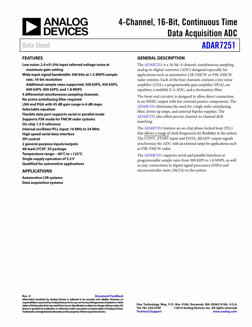
GENERAL DESCRIPTION The ADAR7251 is a 16-bit, 4-channel, simultaneous sampling analog-to-digital converter (ADC) designed especially for applications such as automotive LSR-FMCW or FSK-FMCW radar systems. Each of the four channels contains a low noise amplifier (LNA), a programmable gain amplifier (PGA), an equalizer, a multibit Σ-Δ ADC, and a decimation filter.
The front-end circuitry is designed to allow direct connection to an MMIC output with few external passive components. The ADAR7251 eliminates the need for a high order antialiasing filter, driver op amps, and external bipolar supplies. The ADAR7251 also offers precise channel-to-channel drift matching.
The ADAR7251 features an on-chip phase-locked loop (PLL) that allows a range of clock frequencies for flexibility in the system. The CONV_START input and DATA_READY output signals synchronize the ADC with an external ramp for applications such as FSK-FMCW radar.
The ADAR7251 supports serial and parallel interfaces at programmable sample rates from 300 kSPS to 1.8 MSPS, as well as easy connections to digital signal processors (DSPs) and microcontroller units (MCUs) in the system.

ADAR7251 Data Sheet
Rev. 0 | Page 2 of 72
TABLE OF CONTENTS Features .............................................................................................. 1
Applications ....................................................................................... 1
General Description ......................................................................... 1
Revision History ............................................................................... 3
Functional Block Diagram .............................................................. 4
Specifications ..................................................................................... 5
Analog Channel ............................................................................ 5
Digital Input/Output .................................................................... 6
Power Supply ................................................................................. 7
Digital Filter .................................................................................. 8
SPI Port Timing ............................................................................ 8
Serial/Peripheral Parallel Interface (PPI) Port Timing............ 8
Absolute Maximum Ratings .......................................................... 11
Thermal Resistance .................................................................... 11
ESD Caution ................................................................................ 11
Pin Configuration and Function Descriptions ........................... 12
Typical Performance Characteristics ........................................... 14
Terminology .................................................................................... 17
Theory of Operation ...................................................................... 18
Low Speed Ramp Radar Analog Front End ............................ 18
Main Channel Overview ........................................................... 18
Σ-Δ Modulation and Digital Filtering ..................................... 18
Differential Input Configuration .............................................. 19
Equalizer (EQ) ............................................................................ 19
Using LNA/PGA, EQ, or the Input Capacitor ........................ 20
Reference ..................................................................................... 20
Auxiliary ADC ............................................................................ 20
Power Supply ............................................................................... 21
LDO .............................................................................................. 21
Clock Requirements ................................................................... 21
Crystal Oscillator ........................................................................ 21
PLL ............................................................................................... 21
GPIO ............................................................................................ 23
ADC Data Port ........................................................................... 23
PCB Layout Guidelines .................................................................. 33
Register Summary .......................................................................... 34
Register Details ............................................................................... 37
Clock Control Register .............................................................. 37
PLL Denominator Register ....................................................... 37
PLL Numerator Register ............................................................ 37
PLL Control Register ................................................................. 38
PLL Status Register ..................................................................... 38
Master Enable Switch Register ................................................. 39
ADC Enable Register ................................................................. 39
Power Enable Register ............................................................... 40
Clear the ASIL errors Register .................................................. 41
Selects Which Errors to Mask Register ................................... 42
ASIL Error Flag Register ........................................................... 43
ASIL Error Code Register ......................................................... 43
CRC Value, Bits[7:0] Register ................................................... 44
CRC Value Register .................................................................... 44
Start Calculating the CRC Value of the Register Map Content Register ........................................................................................ 45
Register Map CRC Calculation Done Register ...................... 45
Register Map CRC Value, Bits[7:0] Register ........................... 45
Register Map CRC Value, Bits[15:8] Register ......................... 46
Low Noise Amplifier Gain Control Register .......................... 46
Programmable Gain Amplifier Gain Control Register ......... 47
Signal Path for ADC 1 Through ADC 4 Register .................. 48
Decimator Rate Control Register ............................................. 49
High Pass Filter Control Register ............................................. 50
DAQ Mode Control Register .................................................... 51
Decimator Truncate Control Register ..................................... 52
Serial Output Port Control Register ........................................ 52
Parallel Port Control Register ................................................... 53
ADC Digital Output Mode Register ........................................ 54
Auxiliary ADC Read Value Registers ...................................... 54
Auxiliary ADC Sample Rate Selection Register ..................... 55
Auxiliary ADC Mode Register ................................................. 56
MPx Pin Modes Registers ......................................................... 56
MP Write Value Registers .......................................................... 58
MP Read Value Registers........................................................... 58
SPI_CLK Pin Drive Strength and Slew Rate Register ........... 59
SPI_MISO Pin Drive Strength and Slew Rate Register ......... 60
SPI_SS Pin Drive Strength and Slew Rate Register ............... 60
SPI_MOSI Pin Drive Strength and Slew Rate Register ......... 61
ADDR15 Pin Drive Strength and Slew Rate Register ........... 62
FAULT Pin Drive Strength and Slew Rate Register ............... 62
FS_ADC Pin Drive Strength and Slew Rate Register ............ 63
CONV_START Pin Drive Strength and Slew Rate Register ..... 64

Data Sheet ADAR7251
Rev. 0 | Page 3 of 72
SCLK_ADC Pin Drive Strength and Slew Rate Register ....... 64
ADC_DOUTx Pins Drive Strength and Slew Rate Registers .... 65
DATA_READY Pin Drive Strength and Slew Rate Register ...... 68
XTAL Enable and Drive Register .............................................. 68
ADC Test Register ....................................................................... 69
Digital Filter Sync Enable Register ........................................... 70
CRC Enable/Disable Register .................................................... 70
Typical Application Circuit ............................................................ 71
Outline Dimensions ........................................................................ 72
Ordering Guide ........................................................................... 72
Automotive Products .................................................................. 72
REVISION HISTORY 11/14—Revision 0: Initial Version
ADAR7251 Data Sheet
Rev. 0 | Page 4 of 72
FUNCTIONAL BLOCK DIAGRAM
ADAR7251
CH1 Σ-∆ ADCDIGITALFILTER
AUXIN1AUX ADC
IOV
DD
1,IO
VD
D2
OSCILLATOR
REFERENCEVOLTAGE
REGULATOR
SPICONTROL
XO
UT
XIN
/MC
LK
IN
DIGITALINTERFACE
DE
CIM
AT
OR
S A
DC
MU
X
AIN1PAIN1N
AIN2PAIN2N
AIN3PAIN3N
AIN4PAIN4N
AUXIN2
RE
GO
UT
_DIG
ITA
L
AV
DD
1,A
VD
D2
,AV
DD
3
PLLVDD
ADC_DOUT0
ADC_DOUT1
ADC_DOUT2/GPIO1
ADC_DOUT3/GPIO2
ADC_DOUT4
ADC_DOUT5
ADDR15/ADC_DOUT6
FS_ADC/ADC_DOUT7
SCLK_ADC
CONV_START
DATA_READY
SPI_MISOSPI_MOSISPI_CLKSPI_SS
RESET, PWDN
123
57-0
01
PL
LF
ILT
CM
AVDD
AVDDDVDD
RESET POR
DV
DD
1,D
VD
D2
PL
LG
ND
DG
ND
1, D
GN
D2,
DG
ND
3
AG
ND
1, A
GN
D2
BIAS GENERATOR
PL
LV
DD
PLL
PLLVDD
FAULT
AVDD
AVDD DVDD
LNA PGA EQ
BIASNBIASP
CH2 Σ-∆ ADCDIGITALFILTER
LNA PGA EQ
CH3 Σ-∆ ADCDIGITALFILTER
LNA PGA EQ
CH4 Σ-∆ ADCDIGITALFILTER
LNA PGA EQ
Figure 1.
Data Sheet ADAR7251
Rev. 0 | Page 5 of 72
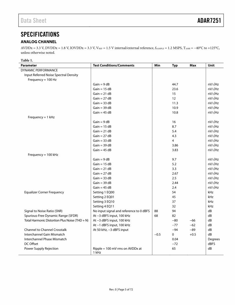
SPECIFICATIONS ANALOG CHANNEL AVDDx = 3.3 V, DVDDx = 1.8 V, IOVDDx = 3.3 V, VREF = 1.5 V internal/external reference, fSAMPLE = 1.2 MSPS, TAMB = −40°C to +125°C, unless otherwise noted.
Table 1. Parameter Test Conditions/Comments Min Typ Max Unit DYNAMIC PERFORMANCE
Input Referred Noise Spectral Density Frequency = 100 Hz
Gain = 9 dB 44.7 nV/√Hz Gain = 15 dB 23.6 nV/√Hz Gain = 21 dB 15 nV/√Hz Gain = 27 dB 12 nV/√Hz Gain = 33 dB 11.3 nV/√Hz Gain = 39 dB 10.9 nV/√Hz Gain = 45 dB 10.8 nV/√Hz
Frequency = 1 kHz Gain = 9 dB 16 nV/√Hz Gain = 15 dB 8.7 nV/√Hz Gain = 21 dB 5.4 nV/√Hz Gain = 27 dB 4.3 nV/√Hz Gain = 33 dB 4 nV/√Hz Gain = 39 dB 3.86 nV/√Hz Gain = 45 dB 3.83 nV/√Hz Frequency = 100 kHz
Gain = 9 dB 9.7 nV/√Hz Gain = 15 dB 5.2 nV/√Hz Gain = 21 dB 3.3 nV/√Hz Gain = 27 dB 2.67 nV/√Hz Gain = 33 dB 2.5 nV/√Hz Gain = 39 dB 2.44 nV/√Hz Gain = 45 dB 2.4 nV/√Hz
Equalizer Corner Frequency Setting 1 EQ00 54 kHz Setting 2 EQ01 45 kHz Setting 3 EQ10 37 kHz Setting 4 EQ11 32 kHz
Signal to Noise Ratio (SNR) No input signal and reference to 0 dBFS 88 94 dB Spurious-Free Dynamic Range (SFDR) At −3 dBFS input, 100 kHz 68 82 dB Total Harmonic Distortion Plus Noise (THD + N) At −3 dBFS input, 100 kHz −80 −66 dB At −1 dBFS input, 100 kHz −77 −62 dB Channel to Channel Crosstalk At 50 kHz, −3 dBFS input −94 −89 dB Interchannel Gain Mismatch −0.5 0 +0.5 dB Interchannel Phase Mismatch 0.04 Degrees DC Offset −72 dBFS Power Supply Rejection Ripple = 100 mV rms on AVDDx at
1 kHz 65 dB
ADAR7251 Data Sheet
Rev. 0 | Page 6 of 72
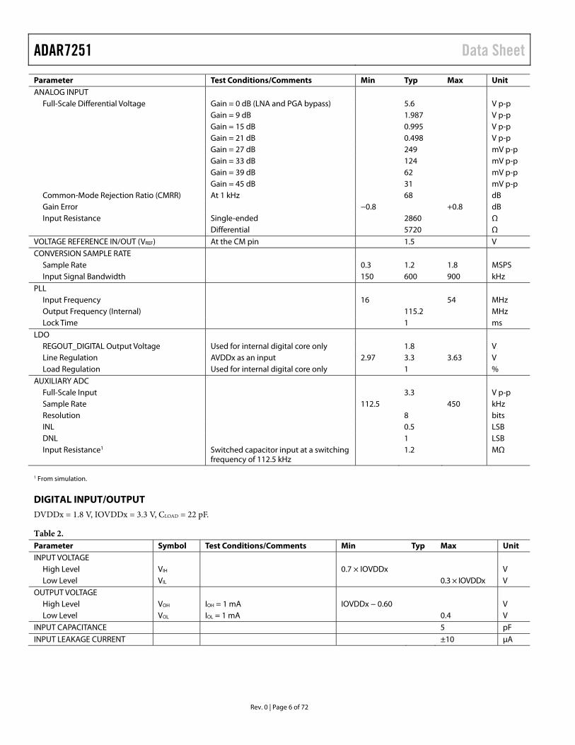
Parameter Test Conditions/Comments Min Typ Max Unit ANALOG INPUT
Full-Scale Differential Voltage Gain = 0 dB (LNA and PGA bypass) 5.6 V p-p Gain = 9 dB 1.987 V p-p Gain = 15 dB 0.995 V p-p Gain = 21 dB 0.498 V p-p Gain = 27 dB 249 mV p-p Gain = 33 dB 124 mV p-p Gain = 39 dB 62 mV p-p Gain = 45 dB 31 mV p-p
Common-Mode Rejection Ratio (CMRR) At 1 kHz 68 dB Gain Error −0.8 +0.8 dB Input Resistance Single-ended 2860 Ω
Differential 5720 Ω VOLTAGE REFERENCE IN/OUT (VREF) At the CM pin 1.5 V CONVERSION SAMPLE RATE
Sample Rate 0.3 1.2 1.8 MSPS Input Signal Bandwidth 150 600 900 kHz
PLL Input Frequency 16 54 MHz Output Frequency (Internal) 115.2 MHz Lock Time 1 ms
LDO REGOUT_DIGITAL Output Voltage Used for internal digital core only 1.8 V Line Regulation AVDDx as an input 2.97 3.3 3.63 V Load Regulation Used for internal digital core only 1 %
AUXILIARY ADC Full-Scale Input 3.3 V p-p Sample Rate 112.5 450 kHz Resolution 8 bits INL 0.5 LSB DNL 1 LSB Input Resistance1 Switched capacitor input at a switching
frequency of 112.5 kHz 1.2 MΩ
1 From simulation.
DIGITAL INPUT/OUTPUT DVDDx = 1.8 V, IOVDDx = 3.3 V, CLOAD = 22 pF.
Table 2. Parameter Symbol Test Conditions/Comments Min Typ Max Unit INPUT VOLTAGE
High Level VIH 0.7 × IOVDDx V Low Level VIL 0.3 × IOVDDx V
OUTPUT VOLTAGE High Level VOH IOH = 1 mA IOVDDx − 0.60 V Low Level VOL IOL = 1 mA 0.4 V
INPUT CAPACITANCE 5 pF INPUT LEAKAGE CURRENT ±10 μA
Data Sheet ADAR7251
Rev. 0 | Page 7 of 72
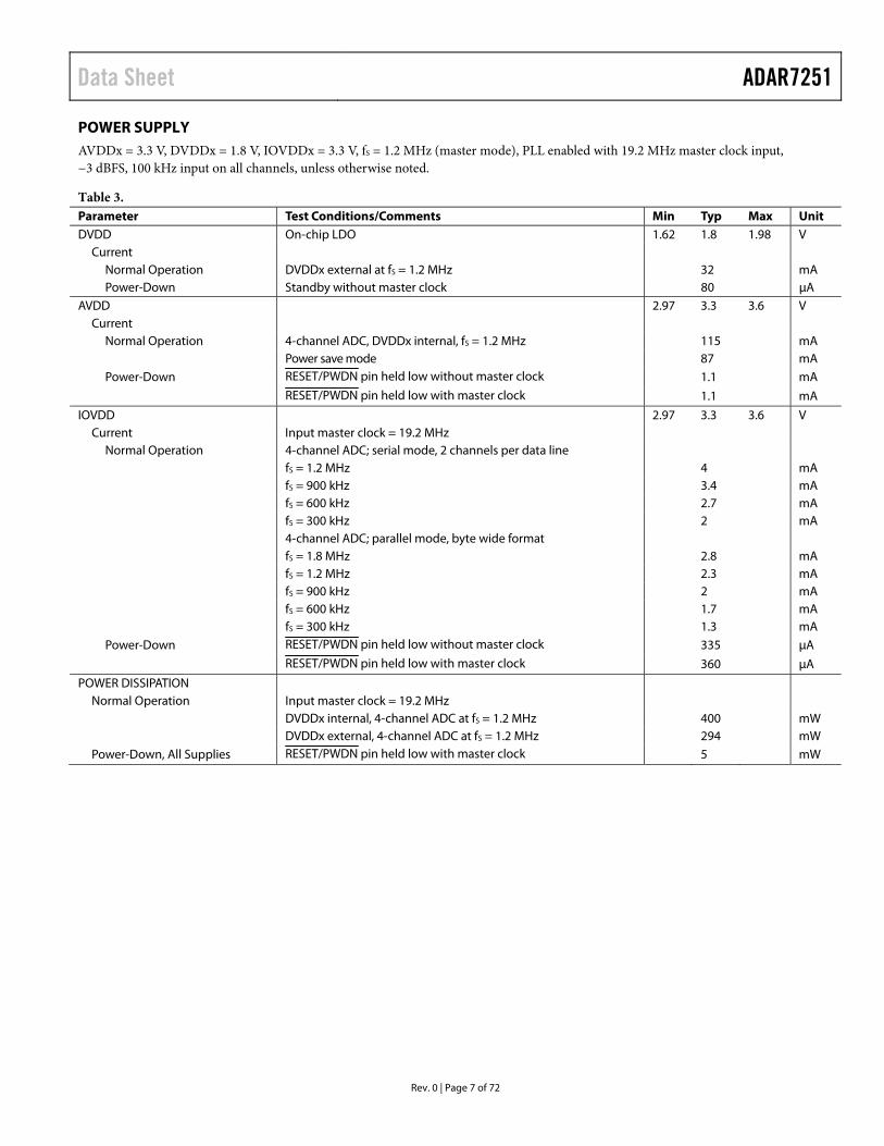
POWER SUPPLY AVDDx = 3.3 V, DVDDx = 1.8 V, IOVDDx = 3.3 V, fS = 1.2 MHz (master mode), PLL enabled with 19.2 MHz master clock input, −3 dBFS, 100 kHz input on all channels, unless otherwise noted.
Table 3. Parameter Test Conditions/Comments Min Typ Max Unit DVDD On-chip LDO 1.62 1.8 1.98 V
Current Normal Operation DVDDx external at fS = 1.2 MHz 32 mA Power-Down Standby without master clock 80 μA
AVDD 2.97 3.3 3.6 V Current
Normal Operation 4-channel ADC, DVDDx internal, fS = 1.2 MHz 115 mA Power save mode 87 mA Power-Down RESET/PWDN pin held low without master clock 1.1 mA
RESET/PWDN pin held low with master clock 1.1 mA
IOVDD 2.97 3.3 3.6 V Current Input master clock = 19.2 MHz
Normal Operation 4-channel ADC; serial mode, 2 channels per data line fS = 1.2 MHz 4 mA
fS = 900 kHz 3.4 mA fS = 600 kHz 2.7 mA fS = 300 kHz 2 mA 4-channel ADC; parallel mode, byte wide format fS = 1.8 MHz 2.8 mA fS = 1.2 MHz 2.3 mA fS = 900 kHz 2 mA fS = 600 kHz 1.7 mA fS = 300 kHz 1.3 mA
Power-Down RESET/PWDN pin held low without master clock 335 μA
RESET/PWDN pin held low with master clock 360 μA
POWER DISSIPATION Normal Operation Input master clock = 19.2 MHz DVDDx internal, 4-channel ADC at fS = 1.2 MHz 400 mW DVDDx external, 4-channel ADC at fS = 1.2 MHz 294 mW Power-Down, All Supplies RESET/PWDN pin held low with master clock 5 mW
ADAR7251 Data Sheet
Rev. 0 | Page 8 of 72
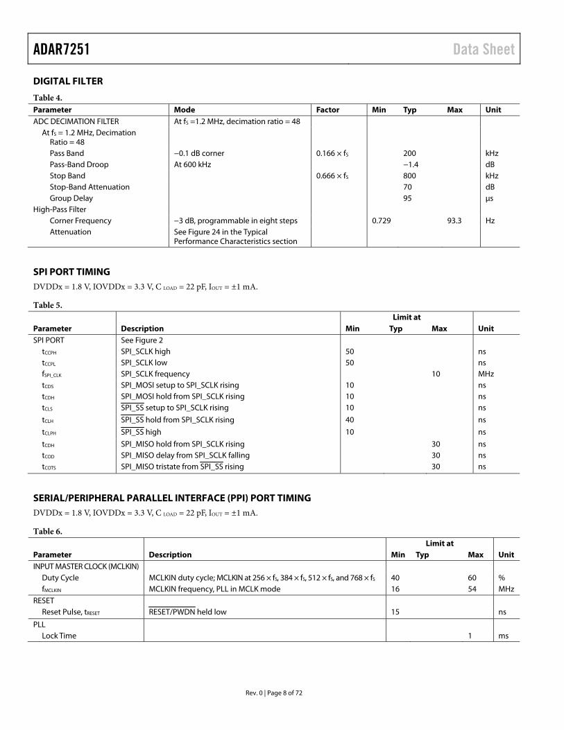
DIGITAL FILTER
Table 4. Parameter Mode Factor Min Typ Max Unit ADC DECIMATION FILTER At fS =1.2 MHz, decimation ratio = 48
At fS = 1.2 MHz, Decimation Ratio = 48
Pass Band −0.1 dB corner 0.166 × fS 200 kHz Pass-Band Droop At 600 kHz −1.4 dB Stop Band 0.666 × fS 800 kHz Stop-Band Attenuation 70 dB Group Delay 95 μs
High-Pass Filter Corner Frequency −3 dB, programmable in eight steps 0.729 93.3 Hz Attenuation See Figure 24 in the Typical
Performance Characteristics section
SPI PORT TIMING DVDDx = 1.8 V, IOVDDx = 3.3 V, C LOAD = 22 pF, IOUT = ±1 mA.
Table 5. Limit at Parameter Description Min Typ Max Unit SPI PORT See Figure 2
tCCPH SPI_SCLK high 50 ns tCCPL SPI_SCLK low 50 ns fSPI_CLK SPI_SCLK frequency 10 MHz tCDS SPI_MOSI setup to SPI_SCLK rising 10 ns tCDH SPI_MOSI hold from SPI_SCLK rising 10 ns tCLS SPI_SS setup to SPI_SCLK rising 10 ns
tCLH SPI_SS hold from SPI_SCLK rising 40 ns
tCLPH SPI_SS high 10 ns
tCDH SPI_MISO hold from SPI_SCLK rising 30 ns tCOD SPI_MISO delay from SPI_SCLK falling 30 ns tCOTS SPI_MISO tristate from SPI_SS rising 30 ns
SERIAL/PERIPHERAL PARALLEL INTERFACE (PPI) PORT TIMING DVDDx = 1.8 V, IOVDDx = 3.3 V, C LOAD = 22 pF, IOUT = ±1 mA.
Table 6. Limit at Parameter Description Min Typ Max Unit INPUT MASTER CLOCK (MCLKIN)
Duty Cycle MCLKIN duty cycle; MCLKIN at 256 × fS, 384 × fS, 512 × fS, and 768 × fS 40 60 % fMCLKIN MCLKIN frequency, PLL in MCLK mode 16 54 MHz
RESET Reset Pulse, tRESET RESET/PWDN held low 15 ns
PLL Lock Time 1 ms
Data Sheet ADAR7251
Rev. 0 | Page 9 of 72
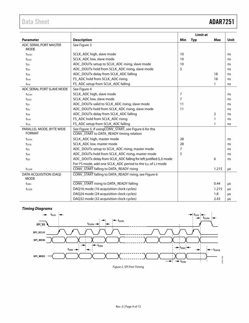
Limit at Parameter Description Min Typ Max Unit ADC SERIAL PORT MASTER
MODE See Figure 3
tSCKH SCLK_ADC high, slave mode 10 ns tSCKL SCLK_ADC low, slave mode 10 ns tDS ADC_DOUTx setup to SCLK_ADC rising, slave mode 10 ns tDH ADC_DOUTx hold from SCLK_ADC rising, slave mode 5 ns tDD ADC_DOUTx delay from SCLK_ADC falling 18 ns tFSH FS_ADC hold from SCLK_ADC rising 18 ns tFSS FS_ADC setup from SCLK_ADC falling 1 ns
ADC SERIAL PORT SLAVE MODE See Figure 4 tSCKH SCLK_ADC high, slave mode 7 ns tSCKL SCLK_ADC low, slave mode 7 ns tDS ADC_DOUTx valid to SCLK_ADC rising, slave mode 11 ns tDH ADC_DOUTx hold from SCLK_ADC rising, slave mode 11 ns tDD ADC_DOUTx delay from SCLK_ADC falling 2 ns tFSH FS_ADC hold from SCLK_ADC rising 1 ns tFSS FS_ADC setup from SCLK_ADC falling 1 ns
PARALLEL MODE, BYTE WIDE FORMAT
See Figure 5; if usingCONV_START, see Figure 6 for the CONV_START to DATA_READY timing relation
tSCKH SCLK_ADC high, master mode 28 ns tSCKL SCLK_ADC low, master mode 28 ns tDS ADC_DOUTx setup to SCLK_ADC rising, master mode 7 ns tDH ADC_DOUTx hold from SCLK_ADC rising, master mode 5 ns tDD ADC_DOUTx delay from SCLK_ADC falling for left justified (LJ) mode 6 ns For I2S mode, add one SCLK_ADC period to the tDD of LJ mode tCSDR CONV_START falling to DATA_READY rising 1.215 μs
DATA ACQUISITION (DAQ) MODE
CONV_START falling to DATA_READY rising, see Figure 6
tDRH CONV_START rising to DATA_READY falling 0.44 μs
tCSDR DAQ16 mode (16 acquisition clock cycles) 1.215 μs DAQ24 mode (24 acquisition clock cycles) 1.8 μs DAQ32 mode (32 acquisition clock cycles) 2.43 μs
Timing Diagrams
SPI_SS
SPI_SCLK
SPI_MOSI
SPI_MISO
tCLS
tCDS
tCDH
tCOD
tCCPH
tCCPL
tCLHtCLPH
tCDH tCOTS
12
357
-00
2
Figure 2. SPI Port Timing
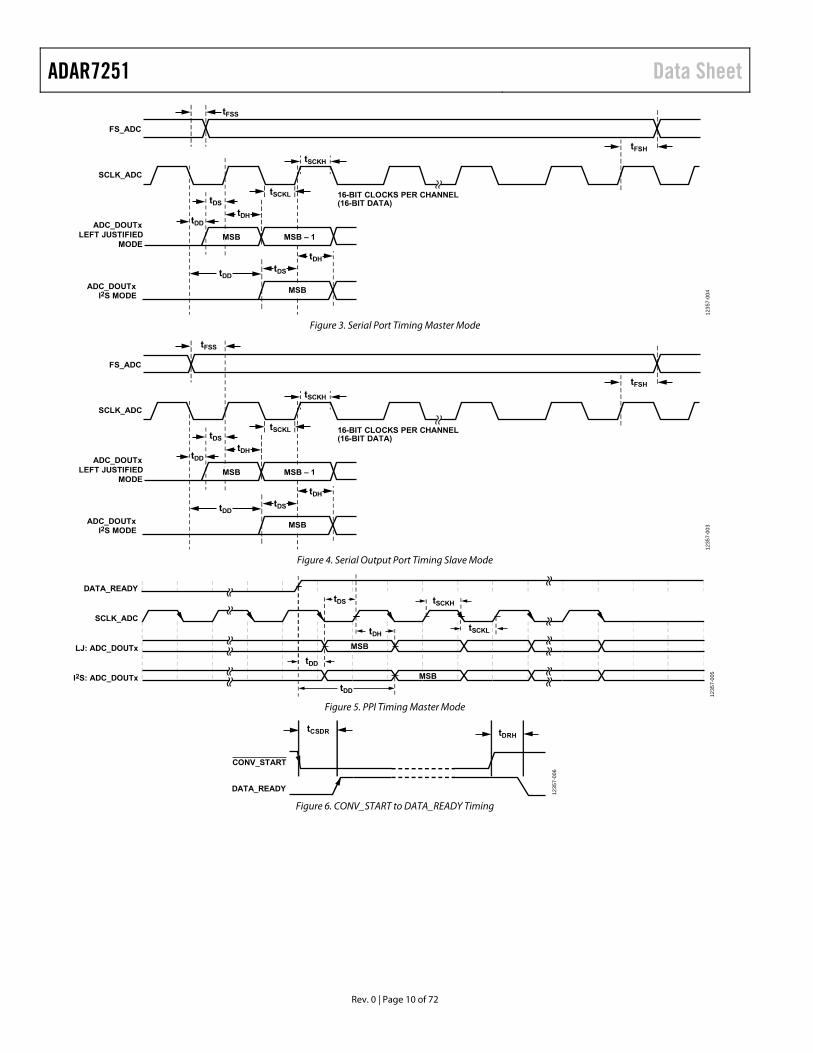
ADAR7251 Data Sheet
Rev. 0 | Page 10 of 72
SCLK_ADC
FS_ADC
ADC_DOUTxLEFT JUSTIFIED
MODE
ADC_DOUTxI2S MODE
16-BIT CLOCKS PER CHANNEL(16-BIT DATA)
tSCKL
tDD
tDD
tSCKH
tFSS
tFSH
tDS
tDS
tDH
tDH
MSB
MSB
MSB – 1
123
57-0
04
Figure 3. Serial Port Timing Master Mode
SCLK_ADC
FS_ADC
ADC_DOUTxLEFT JUSTIFIED
MODE
ADC_DOUTxI2S MODE
16-BIT CLOCKS PER CHANNEL(16-BIT DATA)
tSCKL
tDD
tDD
tSCKH
tFSS
tFSH
tDS
tDS
tDH
tDH
MSB
MSB
MSB – 1
123
57-
003
Figure 4. Serial Output Port Timing Slave Mode
tSCKH
tDHtSCKL
tDS
tDD
tDD
DATA_READY
SCLK_ADC
LJ: ADC_DOUTx
I2S: ADC_DOUTx MSB
MSB
12
357-
005
Figure 5. PPI Timing Master Mode
CONV_START
DATA_READY
tCSDR tDRH
12
357
-00
6
Figure 6. CONV_START to DATA_READY Timing
Data Sheet ADAR7251
Rev. 0 | Page 11 of 72
ABSOLUTE MAXIMUM RATINGS Table 7. Parameter Rating AVDDx to AGNDx, DGNDx −0.3 V to +3.63 V DVDDx to AGNDx, DGNDx −0.3 V to +1.98 V IOVDDx to AGNDx, DGNDx −0.3 V to +3.63 V AGNDx to DGNDx −0.3 V to +0.3 V Analog Input Voltage to AGNDx −0.3 V to +3.63 V Digital Input Voltage to DGNDx −0.3 V to +3.63 V Digital Output Voltage to DGNDx −0.3 V to +3.63 V Input Current to Any Pin Except Supplies ±10 mA Operating Temperature Range (Ambient) −40°C to +125°C Junction Temperature Range −40°C to + 150°C Storage Temperature Range −65°C to +150°C RoHS-Compliant Temperature Soldering
Reflow 260°C
Stresses at or above those listed under Absolute Maximum Ratings may cause permanent damage to the product. This is a stress rating only; functional operation of the product at these or any other conditions above those indicated in the operational section of this specification is not implied. Operation beyond the maximum operating conditions for extended periods may affect product reliability.
THERMAL RESISTANCE θJA represents junction-to-ambient thermal resistance, and θJC represents the junction-to-case thermal resistance. All characteristics are for a standard JEDEC board per JESD51.
Table 8. Thermal Resistance Package Type θJA
1 θJC1 Unit
48-Lead LFCSP_SS 25 1 °C/W
1JEDEC 2S2P standard board.
ESD CAUTION
ADAR7251 Data Sheet
Rev. 0 | Page 12 of 72
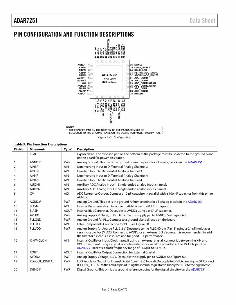
PIN CONFIGURATION AND FUNCTION DESCRIPTIONS
123
DGND3CONV_STARTSCLK_ADC
4 FS_ADC/ADC_DOUT75 ADDR15/ADC_DOUT66 ADC_DOUT57 ADC_DOUT4
24D
VD
D2
23D
GN
D2
22D
AT
A_R
EA
DY
21D
VD
D1
20D
GN
D1
19R
EG
OU
T_D
IGIT
AL
18A
VD
D2
17X
OU
T16
XIN
/MC
LK
IN15
PL
LV
DD
14P
LL
FIL
T13
PL
LG
ND
44A
IN1P
45A
IN1N
46A
IN2P
47A
IN2N
48A
VD
D3
43R
ES
ET
/PW
DN
42F
AU
LT
41S
PI_
SS
40S
PI_
CL
K39
SP
I_M
OS
I38
SP
I_M
ISO
37IO
VD
D2
TOP VIEW(Not to Scale)
ADAR7251
25AVDD126BIASP27BIASN28AGND229CM30AUXIN231AUXIN132AIN4N33AIN4P34AIN3N35AIN3P36AGND1
NOTES1. THE EXPOSED PAD ON THE BOTTOM OF THE PACKAGE MUST BE SOLDERED TO THE GROUND PLANE ON THE BOARD FOR POWER DISSIPATION.
8 ADC_DOUT3/GPIO29 ADC_DOUT2/GPIO1
10 ADC_DOUT111 ADC_DOUT012 IOVDD1
12
357
-007
Figure 7. Pin Configuration
Table 9. Pin Function Descriptions Pin No. Mnemonic Type1 Description
EPAD Exposed Pad. The exposed pad on the bottom of the package must be soldered to the ground plane on the board for power dissipation.
1 AGND12 PWR Analog Ground. This pin is the ground reference point for all analog blocks in the ADAR7251. 2 AIN3P AIN Noninverting Input to Differential Analog Channel 3. 3 AIN3N AIN Inverting Input to Differential Analog Channel 3. 4 AIN4P AIN Noninverting Input to Differential Analog Channel 4. 5 AIN4N AIN Inverting Input to Differential Analog Channel 4. 6 AUXIN1 AIN Auxiliary ADC Analog Input 1. Single-ended analog input channel. 7 AUXIN2 AIN Auxiliary ADC Analog Input 2. Single-ended analog input channel. 8 CM AIO ADC Reference Output. Connect a 10 μF capacitor in parallel with a 100 nF capacitor from this pin to
AGNDx. 9 AGND22 PWR Analog Ground. This pin is the ground reference point for all analog blocks in the ADAR7251. 10 BIASN AOUT Internal Bias Generator. Decouple to AGNDx using a 0.47 μF capacitor. 11 BIASP AOUT Internal Bias Generator. Decouple to AVDDx using a 0.47 μF capacitor. 12 AVDD1 PWR Analog Supply Voltage, 3.3 V. Decouple this supply pin to AGNDx. See Figure 60. 13 PLLGND PWR Analog Ground for PLL. Connect to a ground plane directly on the board. 14 PLLFILT AIN Filter Components Connection for PLL. See Figure 60. 15 PLLVDD PWR Analog Supply for Analog PLL, 3.3 V. Decouple to the PLLGND pin (Pin13) using a 0.1 μF multilayer
ceramic capacitor (MLCC). Connect to AVDDx or an external 3.3 V source. It is recommended to add the filter for a clean 3.3 V source and for good PLL performance.
16 XIN/MCLKIN AIN Internal Oscillator Input/Clock Input. If using an external crystal, connect it between the XIN and XOUT pins. If not using a crystal, a single-ended clock must be provided at the MCLKIN pin. The ADAR7251 accepts a clock frequency range of 16 MHz to 54 MHz.
17 XOUT AOUT Internal Oscillator Output Connection for External Crystal. 18 AVDD2 PWR Analog Supply Voltage, 3.3 V. Decouple this supply pin to AGNDx. See Figure 60. 19 REGOUT_DIGITAL PWR LDO Regulator Output for Internal Digital Core (1.8 V, Typical). Decouple to DGNDx. See Figure 60. Connect
REGOUT_DIGITAL to the DVDDx pins if using the internal regulator to supplythe 1.8 V to the digital core. 20 DGND13 PWR Digital Ground. This pin is the ground reference point for the digital circuitry on the ADAR7251.
Data Sheet ADAR7251
Rev. 0 | Page 13 of 72
Pin No. Mnemonic Type1 Description
21 DVDD1 PWR Digital Core Power Supply Input. Connect decoupling capacitors between the DVDDx and DGNDx pins. See Figure 60. The voltage on this pin is 1.8 V. This pin can be connected to REGOUT_DIGITAL (Pin 19), or to the external 1.8 V source if the internal LDO is not used.
22 DATA_READY DOUT ADC Conversion Data Ready Output. Connect to the DSP general-purpose input/output (GPIO) in the system.
23 DGND23 PWR Digital Ground. This pin is the ground reference point for digital circuitry on the ADAR7251. 24 DVDD2 PWR Digital Core Power Supply Input. Connect decoupling capacitors between the DVDDx and DGNDx
pins. See Figure 60. The voltage on this pin is 1.8 V. This pin can be connected to REGOUT_DIGITAL (Pin 19), or to the external 1.8 V source if the internal LDO is not used.
25 IOVDD1 PWR Logic Power Supply Input. The voltage supplied at this pin determines at what voltage the interface operates. Connect decoupling capacitors between the IOVDDx and DGNDx pins. See Figure 60.
26 ADC_DOUT0 DOUT ADC Data Output (Serial Mode) or ADC Data Output Bit 0 and Bit 8 (PPI Mode). Refer to the ADC Serial Mode and ADC PPI (Byte Wide Mode) sections for function information.
27 ADC_DOUT1 DOUT ADC Data Output (Serial Mode) or ADC Data Output Bit 1/9 (PPI Mode). Refer to the ADC Serial Mode and ADC PPI (Byte Wide Mode) sections for function information.
28 ADC_DOUT2/GPIO1 DOUT ADC Data Output Bit 2 and Bit 10 (PPI Mode)/General-Purpose Input/Output 1. Refer to the ADC Serial Mode section for function information.
29 ADC_DOUT3/GPIO2 DOUT ADC Data Output Bit 3 and Bit 11 (PPI Mode)/General-Purpose Input/Output 2. Refer to the ADC PPI (Byte Wide Mode) section for function information.
30 ADC_DOUT4 DIO ADC Data Output Bit 4 and Bit 12 (PPI Mode). Refer to the ADC PPI (Byte Wide Mode) section for function information.
31 ADC_DOUT5 DIO ADC Data Output Bit 5 and Bit 13 (PPI Mode). Refer to the ADC PPI (Byte Wide Mode) section for function information.
32 ADDR15/ ADC_DOUT6
DIO Device Address Setting for the SPI Control Interface/ADC Data Output Bit 6 and Bit 14 in PPI mode. This pin sets Bit 1 of the SPI device address. Connect to either DGNDx or IOVDDx as desired using a 10 kΩ pull-down or pull-up resistor. Refer to the ADC PPI (Byte Wide Mode) section for function information.
33 FS_ADC/ ADC_DOUT7
DIO Active Low Frame Synchronization Signal for Default ADC Data (Serial Mode)/ADC Data Output Bit 7 and Bit 15 (PPI Mode). Refer to the ADC PPI (Byte Wide Mode) section for function information.
34 SCLK_ADC DIO Serial Bit Clock for the ADC Data Output (Serial Mode and PPI Mode). This pin is an input in slave mode or is an output in master mode.
35 CONV_START DIN ADC Conversion Start in DAQ/PPI/Serial Mode (Active Low). An active low signal initiates an ADC conversion. See the Theory of Operation section for further details.
36 DGND33 PWR Digital Ground. This pin is the ground reference point for digital circuitry on the ADAR7251. 37 IOVDD2 PWR Logic Power Supply Input. The voltage supplied at this pin determines at what voltage the interface
operates. Connect decoupling capacitors between the IOVDDx and DGNDx pins. See Figure 60. 38 SPI_MISO DOUT SPI Control Interface Slave Data Output. 39 SPI_MOSI DIN SPI Control Interface Slave Data Input. 40 SPI_CLK DIN SPI Control Interface Serial clock Input. 41 SPI_SS DIN SPI Control Interface Slave Select (Active Low Input). Connect an external 10 kΩ pull-up resistor to
IOVDDx. 42 FAULT DOUT Digital Output. This pin becomes active under fault condition. Connect an external 10 kΩ pull-up
resistor to IOVDDx. This pin can be used as an interrupt input to the microcontroller or DSP in case of faults.
43 RESET/PWDN DIN Active Low Reset Input/Power-Down. The ADAR7251 requires an external reset signal to hold the RESET input low until AVDDx is within the specified operating range. When held low, this pin places the ADAR7251 into power-down mode.
44 AIN1P AIN Noninverting Input to Differential Analog Channel 1. 45 AIN1N AIN Inverting Input to Differential Analog Channel 1. 46 AIN2P AIN Noninverting Input to Differential Analog Channel 2. 47 AIN2N AIN Inverting Input to Differential Analog Channel 2. 48 AVDD3 PWR Analog Supply Voltage. Decouple this supply pin to AGNDx.
1 PWR is power supply or ground pin, AIN is analog input, AIO is analog input/output, AOUT is analog output, DIN is digital input, DOUT is digital output, and DIO is
digital input/output. 2 All the AGNDx pins (AGND1 and AGND2) are shorted internally and recommended to be connected to a single ground plane on the board. Refer to the PCB Layout
Guidelines section for details. 3 All the DGNDx pins (DGND1, DGND2, and DGND3) are shorted internally and recommended to be connected to a single ground plane on the board. Refer to the PCB
Layout Guidelines section for details.
ADAR7251 Data Sheet
Rev. 0 | Page 14 of 72
TYPICAL PERFORMANCE CHARACTERISTICS 0
–20
–40
–60
–80
–100
–120
–140
–1600 30 60
FREQUENCY (kHz)
AM
PL
ITU
DE
F (
dB
FS
)
90 120 1501
235
7-1
00
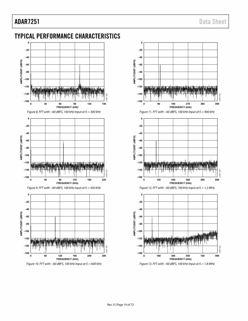
Figure 8. FFT with −60 dBFS, 100 kHz Input at fS = 300 kHz
0
–20
–40
–60
–80
–100
–120
–140
–1600 45 90
FREQUENCY (kHz)
AM
PL
ITU
DE
F (
dB
FS
)
135 180 225
123
57-
101
Figure 9. FFT with −60 dBFS, 100 kHz Input at fS = 450 kHz
0
–20
–40
–60
–80
–100
–120
–140
–1600 60 120
FREQUENCY (kHz)
AM
PL
ITU
DE
F (
dB
FS
)
180 240 300
123
57-
102
Figure 10. FFT with −60 dBFS, 100 kHz Input at fS = 600 kHz
0
–20
–40
–60
–80
–100
–120
–140
–1600 90 180
FREQUENCY (kHz)
AM
PL
ITU
DE
F (
dB
FS
)
270 360 450
123
57-
103
Figure 11. FFT with −60 dBFS, 100 kHz Input at fS = 900 kHz
0
–20
–40
–60
–80
–100
–120
–140
–1600 120 240
FREQUENCY (kHz)
AM
PL
ITU
DE
F (
dB
FS
)
360 480 600
123
57-
104
Figure 12. FFT with −60 dBFS, 100 kHz Input at fS = 1.2 MHz
0
–20
–40
–60
–80
–100
–120
–140
–1600 180 360
FREQUENCY (kHz)
AM
PL
ITU
DE
F (
dB
FS
)
540 720 900
123
57-
105
Figure 13. FFT with −60 dBFS, 100 kHz Input at fS = 1.8 MHz
Data Sheet ADAR7251
Rev. 0 | Page 15 of 72
0
–20
–40
–60
–80
–100
–120
–140
–1600 76 152
FREQUENCY (kHz)
AM
PL
ITU
DE
F (
dB
FS
)
228 304 380
123
57-
110
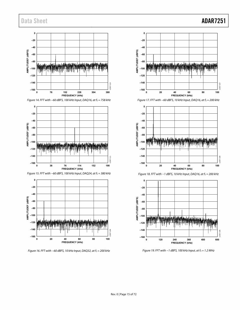
Figure 14. FFT with −60 dBFS, 100 kHz Input, DAQ16, at fS = 758 kHz
0
–20
–40
–60
–80
–100
–120
–140
–1600 38 76
FREQUENCY (kHz)
AM
PL
ITU
DE
F (
dB
FS
)
114 152 190
123
57-
111
Figure 15. FFT with −60 dBFS, 100 kHz Input, DAQ24, at fS = 380 kHz
0
–20
–40
–60
–80
–100
–120
–140
–1600 20 40
FREQUENCY (kHz)
AM
PL
ITU
DE
F (
dB
FS
)
60 80 100
123
57-
109
Figure 16. FFT with −60 dBFS, 10 kHz Input, DAQ32, at fS = 200 kHz
0
–20
–40
–60
–80
–100
–120
–140
–1600 20 40
FREQUENCY (kHz)
AM
PL
ITU
DE
F (
dB
FS
)
60 80 100
123
57-
107
Figure 17. FFT with −60 dBFS, 10 kHz Input, DAQ16, at fS = 200 kHz
0
–20
–40
–60
–80
–100
–120
–140
–1600 20 40
FREQUENCY (kHz)
AM
PL
ITU
DE
F (
dB
FS
)
60 80 100
123
57-
108
Figure 18. FFT with −1 dBFS, 10 kHz Input, DAQ16, at fS = 200 kHz
0
–20
–40
–60
–80
–100
–120
–140
–1600 120 240
FREQUENCY (kHz)
AM
PL
ITU
DE
F (
dB
FS
)
360 480 600
123
57-
106
Figure 19. FFT with −1 dBFS, 100 kHz Input, at fS = 1.2 MHz
ADAR7251 Data Sheet
Rev. 0 | Page 16 of 72
–10
–15
AM
PL
ITU
DE
(d
B) –20
–25
–30
–35
–401 10
FREQUENCY (kHz)100
NO EQ_CAP_CTRLEQ_CAP_CTRL = 00EQ_CAP_CTRL = 01EQ_CAP_CTRL = 10EQ_CAP_CTRL = 11
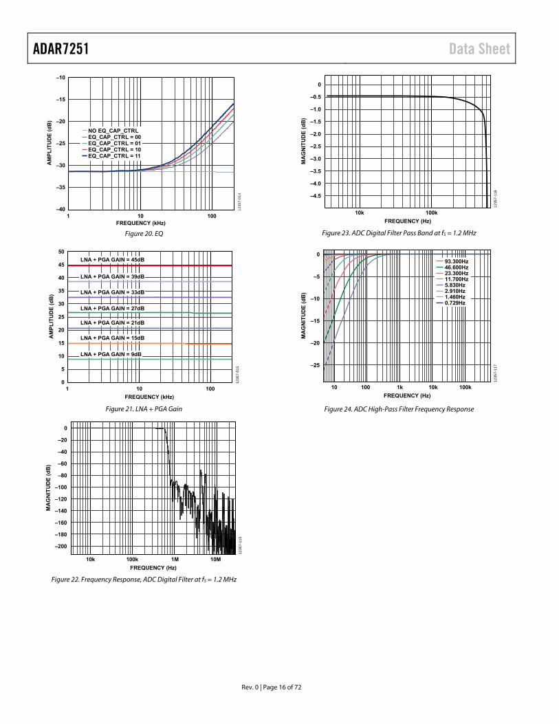
12
357-
01
4Figure 20. EQ
0
5
10
15
20
25
30
35
40
45
50
1 10 100
AM
PL
ITU
DE
(d
B)
FREQUENCY (kHz)
LNA + PGA GAIN = 45dB
LNA + PGA GAIN = 39dB
LNA + PGA GAIN = 33dB
LNA + PGA GAIN = 27dB
LNA + PGA GAIN = 21dB
LNA + PGA GAIN = 15dB
LNA + PGA GAIN = 9dB
1235
7-01
5
Figure 21. LNA + PGA Gain
0
–20
–40
–60
–80
–100
–120
–140
–160
–180
–200
10M1M100k10k
12
357
-11
5
MA
GN
ITU
DE
(d
B)
FREQUENCY (Hz)
Figure 22. Frequency Response, ADC Digital Filter at fS = 1.2 MHz
0
–0.5
–1.0
–1.5
–2.0
–2.5
–3.0
–3.5
–4.0
–4.5
100k10k
12
357
-11
6
FREQUENCY (Hz)
MA
GN
ITU
DE
(d
B)
Figure 23. ADC Digital Filter Pass Band at fS = 1.2 MHz
0
–5
–10
–15
–20
–25
100k10k1k10 100
12
357
-11
7
MA
GN
ITU
DE
(d
B)
FREQUENCY (Hz)
93.300Hz46.600Hz23.300Hz11.700Hz5.830Hz2.910Hz1.460Hz0.729Hz
Figure 24. ADC High-Pass Filter Frequency Response

Data Sheet ADAR7251
Rev. 0 | Page 17 of 72
TERMINOLOGY Integral Nonlinearity (INL) INL is the maximum deviation from a straight line passing through the endpoints of the ADC transfer function. For the ADAR7251, the endpoints of the transfer function are zero scale, a point ½ LSB below the first code transition, and full scale, a point ½ LSB above the last code transition.
Differential Nonlinearity (DNL) DNL is the difference between the measured and the ideal 1 LSB change between any two adjacent codes in the ADC.
Offset Error Offset error is the deviation of the first code transition (00…000) to (00…001) from the ideal (such as ground + 0.5 LSB).
Gain Error For the ADAR7251, gain error is the deviation of the last code transition (111…110) to (111…111) from the ideal (such as VREF – 1.5 LSB) after the offset error is adjusted out.
Signal-to-Noise Ratio (SNR) SNR is the ratio of the rms value of the actual input signal to the rms sum of all other spectral components below the Nyquist frequency, excluding harmonics and dc. The value for SNR is expressed in decibels (dB).
Total Harmonic Distortion (THD) THD is the ratio of the rms sum of harmonics to the fundamental. For the ADAR7251, THD is defined as
1
26
25
24
23
22log20dB
VVVVVV
THD
where: V1 is the rms amplitude of the fundamental. V2, V3, V4, V5, and V6 are the rms amplitudes of the second through the sixth harmonics.
Dynamic Range (DNR) THD + N is measured in dB with an input level of −60 dBFS (−60 dB relative to the full-scale input). Then, 60 dB is added to the measured THD + N value and is expressed in decibels. For example, when measuring 36 dB THD + N with a −60 dBFS input, DNR is 60 + 36 = 96 dB.
Peak Harmonic or Spurious Noise Peak harmonic or spurious noise is defined as the ratio of the rms value of the next largest component in the ADC output spectrum (up to fS/2 and excluding dc) to the rms value of the fundamental. Normally, the value of this specification is determined by the largest harmonic in the spectrum, but for ADCs where the harmonics are buried in the noise floor, it is a noise peak.
ADAR7251 Data Sheet
Rev. 0 | Page 18 of 72
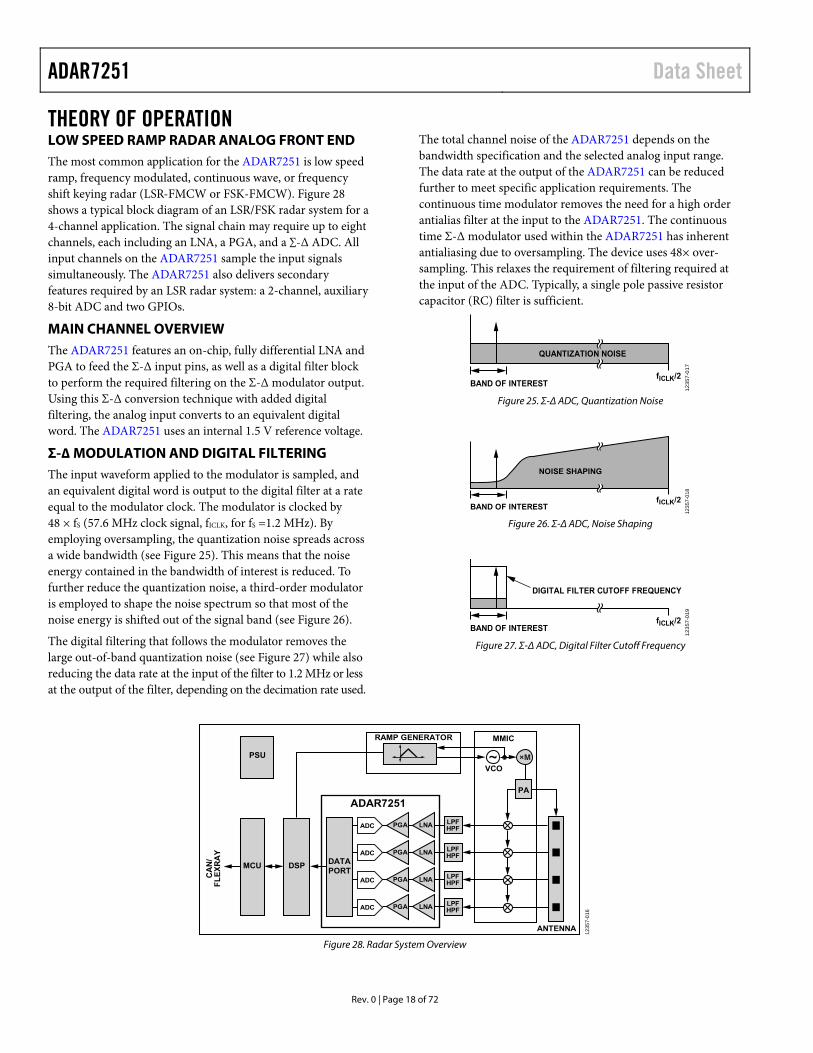
THEORY OF OPERATION LOW SPEED RAMP RADAR ANALOG FRONT END The most common application for the ADAR7251 is low speed ramp, frequency modulated, continuous wave, or frequency shift keying radar (LSR-FMCW or FSK-FMCW). Figure 28 shows a typical block diagram of an LSR/FSK radar system for a 4-channel application. The signal chain may require up to eight channels, each including an LNA, a PGA, and a ∑-Δ ADC. All input channels on the ADAR7251 sample the input signals simultaneously. The ADAR7251 also delivers secondary features required by an LSR radar system: a 2-channel, auxiliary 8-bit ADC and two GPIOs.
MAIN CHANNEL OVERVIEW The ADAR7251 features an on-chip, fully differential LNA and PGA to feed the Σ-Δ input pins, as well as a digital filter block to perform the required filtering on the Σ-Δ modulator output. Using this Σ-Δ conversion technique with added digital filtering, the analog input converts to an equivalent digital word. The ADAR7251 uses an internal 1.5 V reference voltage.
Σ-∆ MODULATION AND DIGITAL FILTERING The input waveform applied to the modulator is sampled, and an equivalent digital word is output to the digital filter at a rate equal to the modulator clock. The modulator is clocked by 48 × fS (57.6 MHz clock signal, fICLK, for fS =1.2 MHz). By employing oversampling, the quantization noise spreads across a wide bandwidth (see Figure 25). This means that the noise energy contained in the bandwidth of interest is reduced. To further reduce the quantization noise, a third-order modulator is employed to shape the noise spectrum so that most of the noise energy is shifted out of the signal band (see Figure 26).
The digital filtering that follows the modulator removes the large out-of-band quantization noise (see Figure 27) while also reducing the data rate at the input of the filter to 1.2 MHz or less at the output of the filter, depending on the decimation rate used.
The total channel noise of the ADAR7251 depends on the bandwidth specification and the selected analog input range. The data rate at the output of the ADAR7251 can be reduced further to meet specific application requirements. The continuous time modulator removes the need for a high order antialias filter at the input to the ADAR7251. The continuous time Σ-Δ modulator used within the ADAR7251 has inherent antialiasing due to oversampling. The device uses 48× over-sampling. This relaxes the requirement of filtering required at the input of the ADC. Typically, a single pole passive resistor capacitor (RC) filter is sufficient.
QUANTIZATION NOISE
fICLK/2BAND OF INTEREST
12
35
7-0
17
Figure 25. Σ-Δ ADC, Quantization Noise
fICLK/2
NOISE SHAPING
BAND OF INTEREST
12
35
7-0
18
Figure 26. Σ-Δ ADC, Noise Shaping
fICLK/2BAND OF INTEREST
DIGITAL FILTER CUTOFF FREQUENCY
12
35
7-0
19
Figure 27. Σ-Δ ADC, Digital Filter Cutoff Frequency
×M
PA
MMIC
VCO
ANTENNA
RAMP GENERATOR
DSPMCU DATAPORT
ADCLPFHPF
CA
N/
FL
EX
RA
Y
PSU
ADAR7251
PGA LNA
ADCLPFHPFPGA LNA
ADCLPFHPFPGA LNA
ADCLPFHPFPGA LNA
1235
7-0
16
Figure 28. Radar System Overview
Data Sheet ADAR7251
Rev. 0 | Page 19 of 72
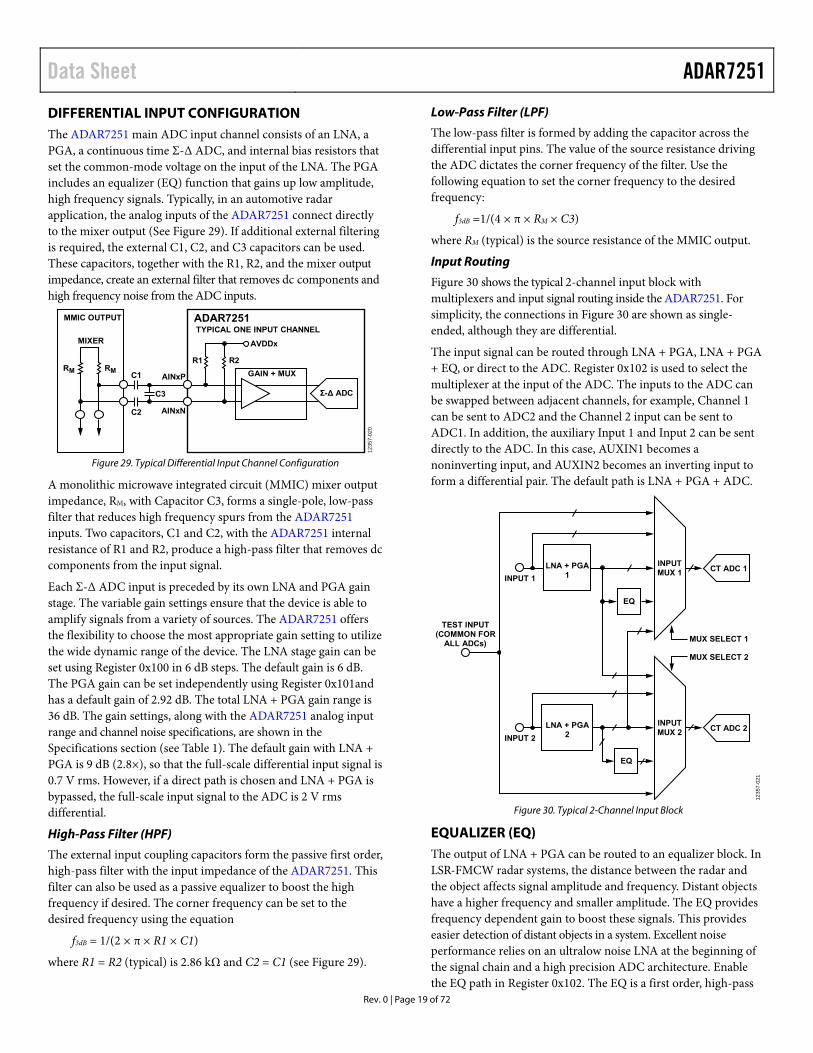
DIFFERENTIAL INPUT CONFIGURATION The ADAR7251 main ADC input channel consists of an LNA, a PGA, a continuous time Σ-Δ ADC, and internal bias resistors that set the common-mode voltage on the input of the LNA. The PGA includes an equalizer (EQ) function that gains up low amplitude, high frequency signals. Typically, in an automotive radar application, the analog inputs of the ADAR7251 connect directly to the mixer output (See Figure 29). If additional external filtering is required, the external C1, C2, and C3 capacitors can be used. These capacitors, together with the R1, R2, and the mixer output impedance, create an external filter that removes dc components and high frequency noise from the ADC inputs.
Σ-∆ ADC
AINxP
AINxN
C1
R1 R2
C3
C2
RM RM
MIXER
ADAR7251
AVDDx
GAIN + MUX
MMIC OUTPUT
TYPICAL ONE INPUT CHANNEL
1235
7-02
0
Figure 29. Typical Differential Input Channel Configuration
A monolithic microwave integrated circuit (MMIC) mixer output impedance, RM, with Capacitor C3, forms a single-pole, low-pass filter that reduces high frequency spurs from the ADAR7251 inputs. Two capacitors, C1 and C2, with the ADAR7251 internal resistance of R1 and R2, produce a high-pass filter that removes dc components from the input signal.
Each Σ-Δ ADC input is preceded by its own LNA and PGA gain stage. The variable gain settings ensure that the device is able to amplify signals from a variety of sources. The ADAR7251 offers the flexibility to choose the most appropriate gain setting to utilize the wide dynamic range of the device. The LNA stage gain can be set using Register 0x100 in 6 dB steps. The default gain is 6 dB. The PGA gain can be set independently using Register 0x101and has a default gain of 2.92 dB. The total LNA + PGA gain range is 36 dB. The gain settings, along with the ADAR7251 analog input range and channel noise specifications, are shown in the Specifications section (see Table 1). The default gain with LNA + PGA is 9 dB (2.8×), so that the full-scale differential input signal is 0.7 V rms. However, if a direct path is chosen and LNA + PGA is bypassed, the full-scale input signal to the ADC is 2 V rms differential.
High-Pass Filter (HPF)
The external input coupling capacitors form the passive first order, high-pass filter with the input impedance of the ADAR7251. This filter can also be used as a passive equalizer to boost the high frequency if desired. The corner frequency can be set to the desired frequency using the equation
f3dB = 1/(2 × π × R1 × C1)
where R1 = R2 (typical) is 2.86 kΩ and C2 = C1 (see Figure 29).
Low-Pass Filter (LPF)
The low-pass filter is formed by adding the capacitor across the differential input pins. The value of the source resistance driving the ADC dictates the corner frequency of the filter. Use the following equation to set the corner frequency to the desired frequency:
f3dB =1/(4 × π × RM × C3)
where RM (typical) is the source resistance of the MMIC output.
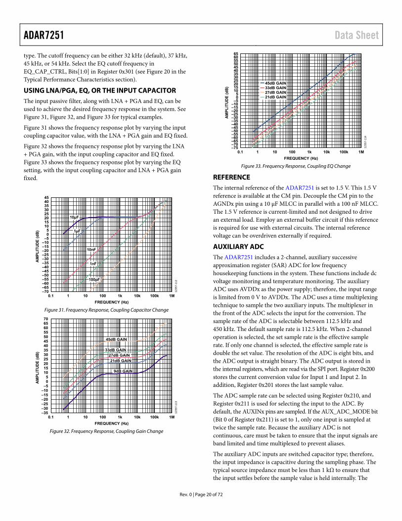
Input Routing
Figure 30 shows the typical 2-channel input block with multiplexers and input signal routing inside the ADAR7251. For simplicity, the connections in Figure 30 are shown as single-ended, although they are differential.
The input signal can be routed through LNA + PGA, LNA + PGA + EQ, or direct to the ADC. Register 0x102 is used to select the multiplexer at the input of the ADC. The inputs to the ADC can be swapped between adjacent channels, for example, Channel 1 can be sent to ADC2 and the Channel 2 input can be sent to ADC1. In addition, the auxiliary Input 1 and Input 2 can be sent directly to the ADC. In this case, AUXIN1 becomes a noninverting input, and AUXIN2 becomes an inverting input to form a differential pair. The default path is LNA + PGA + ADC.
EQ
MUX SELECT 1
INPUTMUX 1 CT ADC 1
EQ
INPUTMUX 2 CT ADC 2
MUX SELECT 2
LNA + PGA1
LNA + PGA2
INPUT 1
INPUT 2
TEST INPUT(COMMON FOR
ALL ADCs)
123
57-0
21
Figure 30. Typical 2-Channel Input Block
EQUALIZER (EQ) The output of LNA + PGA can be routed to an equalizer block. In LSR-FMCW radar systems, the distance between the radar and the object affects signal amplitude and frequency. Distant objects have a higher frequency and smaller amplitude. The EQ provides frequency dependent gain to boost these signals. This provides easier detection of distant objects in a system. Excellent noise performance relies on an ultralow noise LNA at the beginning of the signal chain and a high precision ADC architecture. Enable the EQ path in Register 0x102. The EQ is a first order, high-pass
ADAR7251 Data Sheet
Rev. 0 | Page 20 of 72
type. The cutoff frequency can be either 32 kHz (default), 37 kHz, 45 kHz, or 54 kHz. Select the EQ cutoff frequency in EQ_CAP_CTRL, Bits[1:0] in Register 0x301 (see Figure 20 in the Typical Performance Characteristics section).
USING LNA/PGA, EQ, OR THE INPUT CAPACITOR The input passive filter, along with LNA + PGA and EQ, can be used to achieve the desired frequency response in the system. See Figure 31, Figure 32, and Figure 33 for typical examples.
Figure 31 shows the frequency response plot by varying the input coupling capacitor value, with the LNA + PGA gain and EQ fixed.
Figure 32 shows the frequency response plot by varying the LNA + PGA gain, with the input coupling capacitor and EQ fixed. Figure 33 shows the frequency response plot by varying the EQ setting, with the input coupling capacitor and LNA + PGA gain fixed.
–70–65–60–55–50–45–40–35–30–25–20–15–10
–505
1015202530354045
0.1 1 10 100
AM
PL
ITU
DE
(d
B)
1k 10k 100k 1M
FREQUENCY (Hz)
10µF
1µF
1nF
10nF
100pF
123
57-1
12
Figure 31. Frequency Response, Coupling Capacitor Change
0.1 1 10 100
AM
PL
ITU
DE
(d
B)
1k 10k 100k 1M
FREQUENCY (Hz)
123
57-1
13
45dB GAIN
33dB GAIN27dB GAIN21dB GAIN
9dB GAIN
–35–30–25–20–15–10
–5
1050
152025303540455055606570
Figure 32. Frequency Response, Coupling Gain Change
–75–70–65–60–55–50–45–40–35–30–25–20–15–10
–505
101520253035404550556065
0.1 1 10 100
AM
PL
ITU
DE
(d
B)
1k 10k 100k 1M
FREQUENCY (Hz)
33dB GAIN45dB GAIN
27dB GAIN21dB GAIN
123
57-1
14
Figure 33. Frequency Response, Coupling EQ Change
REFERENCE The internal reference of the ADAR7251 is set to 1.5 V. This 1.5 V reference is available at the CM pin. Decouple the CM pin to the AGNDx pin using a 10 μF MLCC in parallel with a 100 nF MLCC. The 1.5 V reference is current-limited and not designed to drive an external load. Employ an external buffer circuit if this reference is required for use with external circuits. The internal reference voltage can be overdriven externally if required.
AUXILIARY ADC The ADAR7251 includes a 2-channel, auxiliary successive approximation register (SAR) ADC for low frequency housekeeping functions in the system. These functions include dc voltage monitoring and temperature monitoring. The auxiliary ADC uses AVDDx as the power supply; therefore, the input range is limited from 0 V to AVDDx. The ADC uses a time multiplexing technique to sample the two auxiliary inputs. The multiplexer in the front of the ADC selects the input for the conversion. The sample rate of the ADC is selectable between 112.5 kHz and 450 kHz. The default sample rate is 112.5 kHz. When 2-channel operation is selected, the set sample rate is the effective sample rate. If only one channel is selected, the effective sample rate is double the set value. The resolution of the ADC is eight bits, and the ADC output is straight binary. The ADC output is stored in the internal registers, which are read via the SPI port. Register 0x200 stores the current conversion value for Input 1 and Input 2. In addition, Register 0x201 stores the last sample value.
The ADC sample rate can be selected using Register 0x210, and Register 0x211 is used for selecting the input to the ADC. By default, the AUXINx pins are sampled. If the AUX_ADC_MODE bit (Bit 0 of Register 0x211) is set to 1, only one input is sampled at twice the sample rate. Because the auxiliary ADC is not continuous, care must be taken to ensure that the input signals are band limited and time multiplexed to prevent aliases.
The auxiliary ADC inputs are switched capacitor type; therefore, the input impedance is capacitive during the sampling phase. The typical source impedance must be less than 1 kΩ to ensure that the input settles before the sample value is held internally. The
Data Sheet ADAR7251
Rev. 0 | Page 21 of 72
source driving the ADC inputs must be able to drive at least 20 pF, excluding the parasitic capacitance on the board.
AUXIN1
AUX ADC
AUXIN2
12
357
-02
2
Figure 34. Auxiliary ADC
POWER SUPPLY The ADAR7251 uses three supplies: 3.3 V for AVDDx, 1.8 V for DVDDx, and 3.3 V for IOVDDx. AVDDx and IOVDDx must be supplied to the device, but the supply to the DVDDx pins can be either generated by an internal LDO, or provided externally by turning off the LDO.
The AVDDx pins supply the analog core of the ADC, and the DVDDx pins supply the digital core of the ADC. The IOVDDx pins supply the digital input/output pins of the ADAR7251.
Decouple all power supplies to ground with a 0.1 μF and a 10 μF X7R MLCC for best ADC performance. The device provides the exposed pad underneath, which must be connected to the ground plane with thermal vias. All the ground pins must be connected to the single ground plane on the PCB with the shortest possible path close to the respective pins.
LDO The internal LDO generates the DVDDx voltage (1.8 V) required for the digital core. The LDO takes the AVDDx (3.3 V) supply and regulates down to 1.8 V. External decoupling capacitors are required to ensure clean power to the digital core. If using the internal 1.8 V supply for the digital core, the REGOUT_DIGITAL pin must be externally connected to the DVDDx pins. The 1 nF MLCC, in parallel with 0.1 μF and 10 μF capacitors, are recom-mended at the DVDDx pins to decouple the high frequency noise.
CLOCK REQUIREMENTS To achieve the specified dynamic performance, use an external crystal at the XIN/MCLKIN and XOUT pins. Alternatively, provide the single-ended clock at the MCLKIN input via an MCU/DSP controller. The ADAR7251 features an internal PLL block that accepts the clock frequency in a range of 16 MHz to 54 MHz, via either the clock available in the system, or an external crystal. An external clock must be connected to the XIN/ MCLKIN pin and must be within the 0 V to 3.3 V p-p.
CRYSTAL OSCILLATOR The external quartz crystal can be connected across the XIN and XOUT pins. When using the crystal, use Register 0x292 to enable the crystal oscillator block. The output of the crystal oscillator is an input to the PLL. The typical supported frequency range is 16 MHz to 54 MHz. Select load capacitors C1 and C2 for the crystal based on the recommendation of the crystal manufacturer. Determine the value of R1 based on the crystal current rating.
ADAR7251
XIN
Y1 R1
C1 C2
XOUT
12
35
7-0
23
Figure 35. Crystal Oscillator
PLL The PLL provides the stable clock for the internal blocks. It uses the clock input at the XIN/MCLKIN pin as a reference to generate the core clock. Set the PLL for either integer or fractional mode. The PLL multipliers and dividers (X, R, M, and N) are programmed using Register 0x000 to Register 0x003. The PLL can accept input frequencies in the range of 16 MHz to 54 MHz, either directly from an external source, or using the crystal connected at the XIN/MCLKIN and XOUT pins. The PLL output frequency is fixed at 115.2 MHz.
÷X
ADC CLOCK
INTERNAL PLL OUTPUT115.2MHzx (R + N ÷ M)
÷2
XIN
PLL
12
357
-02
4
Figure 36. PLL Block Diagram
The PLL requires an external loop filter, which is fixed (see Figure 37). For temperature sensitive applications, the loop filter components must be appropriate. The PLL loop filter capacitors must be NPO type for best temperature performance.
PLLFILT
PLLGND
390pF
5.6nF
1kΩ
123
57-0
25
Figure 37. PLL Loop Filter
Place the PLL loop filter close to the PLLFILT pin to prevent crosstalk from other sources on the board. In addition, take care to decouple the PLLVDD supply to the PLL. It is recommended that X7R MLCC or better dielectric MLCCs of 1 nF be added in parallel with 0.1 μF and 10 μF capacitors close to the PLLVDD pin. See the PCB Layout Guidelines section for details.
ADAR7251 Data Sheet
Rev. 0 | Page 22 of 72
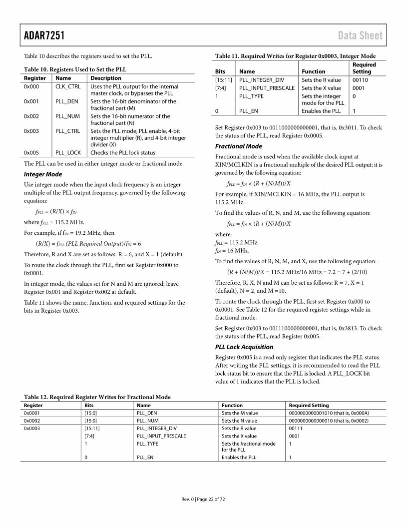
Table 10 describes the registers used to set the PLL.
Table 10. Registers Used to Set the PLL Register Name Description 0x000 CLK_CTRL Uses the PLL output for the internal
master clock, or bypasses the PLL 0x001 PLL_DEN Sets the 16-bit denominator of the
fractional part (M) 0x002 PLL_NUM Sets the 16-bit numerator of the
fractional part (N) 0x003 PLL_CTRL Sets the PLL mode, PLL enable, 4-bit
integer multiplier (R), and 4-bit integer divider (X)
0x005 PLL_LOCK Checks the PLL lock status
The PLL can be used in either integer mode or fractional mode.
Integer Mode
Use integer mode when the input clock frequency is an integer multiple of the PLL output frequency, governed by the following equation:
fPLL = (R/X) × fIN
where fPLL = 115.2 MHz.
For example, if fIN = 19.2 MHz, then
(R/X) = fPLL (PLL Required Output)/fIN = 6
Therefore, R and X are set as follows: R = 6, and X = 1 (default).
To route the clock through the PLL, first set Register 0x000 to 0x0001.
In integer mode, the values set for N and M are ignored; leave Register 0x001 and Register 0x002 at default.
Table 11 shows the name, function, and required settings for the bits in Register 0x003.
Table 11. Required Writes for Register 0x0003, Integer Mode
Bits Name Function Required Setting
[15:11] PLL_INTEGER_DIV Sets the R value 00110 [7:4] PLL_INPUT_PRESCALE Sets the X value 0001 1 PLL_TYPE Sets the integer
mode for the PLL 0
0 PLL_EN Enables the PLL 1
Set Register 0x003 to 0011000000000001, that is, 0x3011. To check the status of the PLL, read Register 0x0005.
Fractional Mode
Fractional mode is used when the available clock input at XIN/MCLKIN is a fractional multiple of the desired PLL output; it is governed by the following equation:
fPLL = fIN × (R + (N/M))/X
For example, if XIN/MCLKIN = 16 MHz, the PLL output is 115.2 MHz.
To find the values of R, N, and M, use the following equation:
fPLL = fIN × (R + (N/M))/X
where: fPLL = 115.2 MHz. fIN = 16 MHz.
To find the values of R, N, M, and X, use the following equation:
(R + (N/M))/X = 115.2 MHz/16 MHz = 7.2 = 7 + (2/10)
Therefore, R, X, N and M can be set as follows: R = 7, X = 1 (default), N = 2, and M =10.
To route the clock through the PLL, first set Register 0x000 to 0x0001. See Table 12 for the required register settings while in fractional mode.
Set Register 0x003 to 0011100000000001, that is, 0x3813. To check the status of the PLL, read Register 0x005.
PLL Lock Acquisition
Register 0x005 is a read only register that indicates the PLL status. After writing the PLL settings, it is recommended to read the PLL lock status bit to ensure that the PLL is locked. A PLL_LOCK bit value of 1 indicates that the PLL is locked.
Table 12. Required Register Writes for Fractional Mode Register Bits Name Function Required Setting
0x0001 [15:0] PLL_DEN Sets the M value 0000000000001010 (that is, 0x000A)
0x0002 [15:0] PLL_NUM Sets the N value 0000000000000010 (that is, 0x0002)
0x0003 [15:11] PLL_INTEGER_DIV Sets the R value 00111
[7:4] PLL_INPUT_PRESCALE Sets the X value 0001
1 PLL_TYPE Sets the fractional mode for the PLL
1
0 PLL_EN Enables the PLL 1
Data Sheet ADAR7251
Rev. 0 | Page 23 of 72
GPIO The ADAR7251 contains two GPIOs: Pin 28 and Pin 29. These pins are dual function. They serve as ADC data output pins in PPI mode, or as GPIOs in serial mode. These pins can be configured as inputs or outputs, and are read back or programmed via the SPI control interface. Register 0x250 and Register 0x251 are used for setting GPIO1 and GPIO2, respectively. Typical applications for these pins include monitoring the status of logic signals or controlling external devices. Use the GPIO pins for low speed serial communication. Configure the GPIO pins by writing to the GPIO configuration registers, Register 0x250 and Register 0x251. Note that, in these registers, the GPIO pins are referred to as the multipurpose (MPx) pins, Each GPIO pin has associated bits in the GPIO configuration register that define a status of the pin and whether the GPIO is used as an input or an output, as well as the debounce period. Register 0x260 and Register 0x261 can be used to output 1 or 0 to GPIO1 and GPIO2, respectively. Register 0x270 and Register 0x271 provide the read value from GPIO1 and GPIO2, respectively.
ADC DATA PORT The ADAR7251 digital interface port provides multiple options for accessing the ADC data and connecting to DSP or micro-controllers in the system. The digital interface port can be set as serial mode or parallel mode.
Note that, throughout the remainder of the data sheet, multifunction pins are referred to by the relevant function in text and figures, where applicable.
ADC Serial Mode
The ADC serial port uses the conversion start pin (CONV_START), the frame sync pin (FS_ADC/ADC_DOUT7), the bit clock pin (SCLK_ADC), and two data output pins (ADC_DOUT0 and ADC_DOUT1). CONV_START can be disabled if it is not required in the system. The serial port can be set to either master or slave mode. The ADC output data is twos complement, 16-bit binary. Depending on the mode setup, the frame sync and bit clock pin directions change. In master mode, the ADAR7251 generates these signals, whereas in slave mode, these signals are provided by the external DSP. The ADC_DOUT0 and ADC_DOUT1 pins are always set as outputs, independent of the master or slave mode. The data format is fixed to MSB first. The serial port is powered using the IOVDDx supply. Take proper care to ensure decoupling of the high frequency noise on this pin to prevent jitter on the clock and data outputs. Connect a 100 nF MLCC is recommended to be connected to the IOVDDx pins as close as possible with direct connection to the DGNDx pins and a ground plane on the board.
Because the bit clock rate is in the 40 MHz range, traces on the board require proper attention. The bit clock and data pin (ADC_DOUTx) must be traced out with transmission line considerations. If the clock is connected to multiple devices, the stubs must be properly terminated to reduce reflections. Microstrip or stripline traces are recommended for these pins. Increase the
drive strength for the digital output pins using Register 0x0280 through Register 0x292. The ADAR7251 consists of four ADCs. Data is available in two pairs on the ADC_DOUT0 and ADC_DOUT1 pins: Channel 1 and Channel 2 on ADC_DOUT0, and Channel3 and Channel 4 on ADC_DOUT1 in 2-channel mode. Each channel uses 16 bits; for two channels, 32-bit clocks are required. The frame sync signal (FS_ADC) sets the sample rate for the ADC. Therefore, the typical bit clock rate for a sample rate of 1.2 MHz is
32 × 1.2 MHz = 38.4 MHz
ADC Serial Master Mode
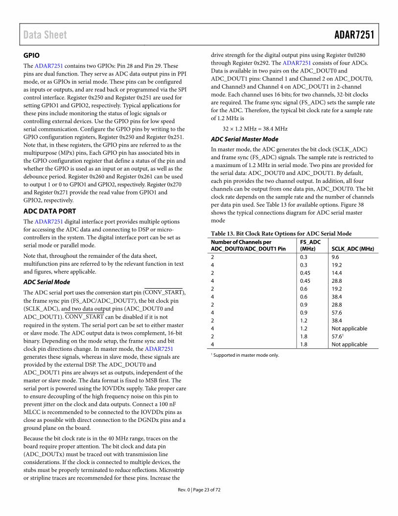
In master mode, the ADC generates the bit clock (SCLK_ADC) and frame sync (FS_ADC) signals. The sample rate is restricted to a maximum of 1.2 MHz in serial mode. Two pins are provided for the serial data: ADC_DOUT0 and ADC_DOUT1. By default, each pin provides the two channel output. In addition, all four channels can be output from one data pin, ADC_DOUT0. The bit clock rate depends on the sample rate and the number of channels per data pin used. See Table 13 for available options. Figure 38 shows the typical connections diagram for ADC serial master mode
Table 13. Bit Clock Rate Options for ADC Serial Mode Number of Channels per ADC_DOUT0/ADC_DOUT1 Pin
FS_ADC (MHz) SCLK_ADC (MHz)
2 0.3 9.6 4 0.3 19.2 2 0.45 14.4 4 0.45 28.8 2 0.6 19.2 4 0.6 38.4 2 0.9 28.8 4 0.9 57.6 2 1.2 38.4 4 1.2 Not applicable 2 1.8 57.61
4 1.8 Not applicable 1 Supported in master mode only.
ADAR7251 Data Sheet
Rev. 0 | Page 24 of 72
SCLK_ADC/ADC_DOUT7
FS_ADC
ADC_DOUT0
SLAVE DSPADAR7251
MASTER
ADAR7251MASTER
XIN
/MC
LK
IN
XO
UT
XI/
MC
LK
INN
XO
UT
SP
OR
T1
SP
OR
T2
OPTIONAL FOR > 4 CHANNELS
MCLKIN
ADC_DOUT1
SCLK_ADC/ADC_DOUT7
FS_ADC
ADC_DOUT0
ADC_DOUT1
OSCILLATOR
123
57-0
26
Figure 38. Typical Connection Diagram for ADC Serial Master Mode
Figure 41 and Figure 42 show the waveforms for the serial modes without the CONV_START signal.
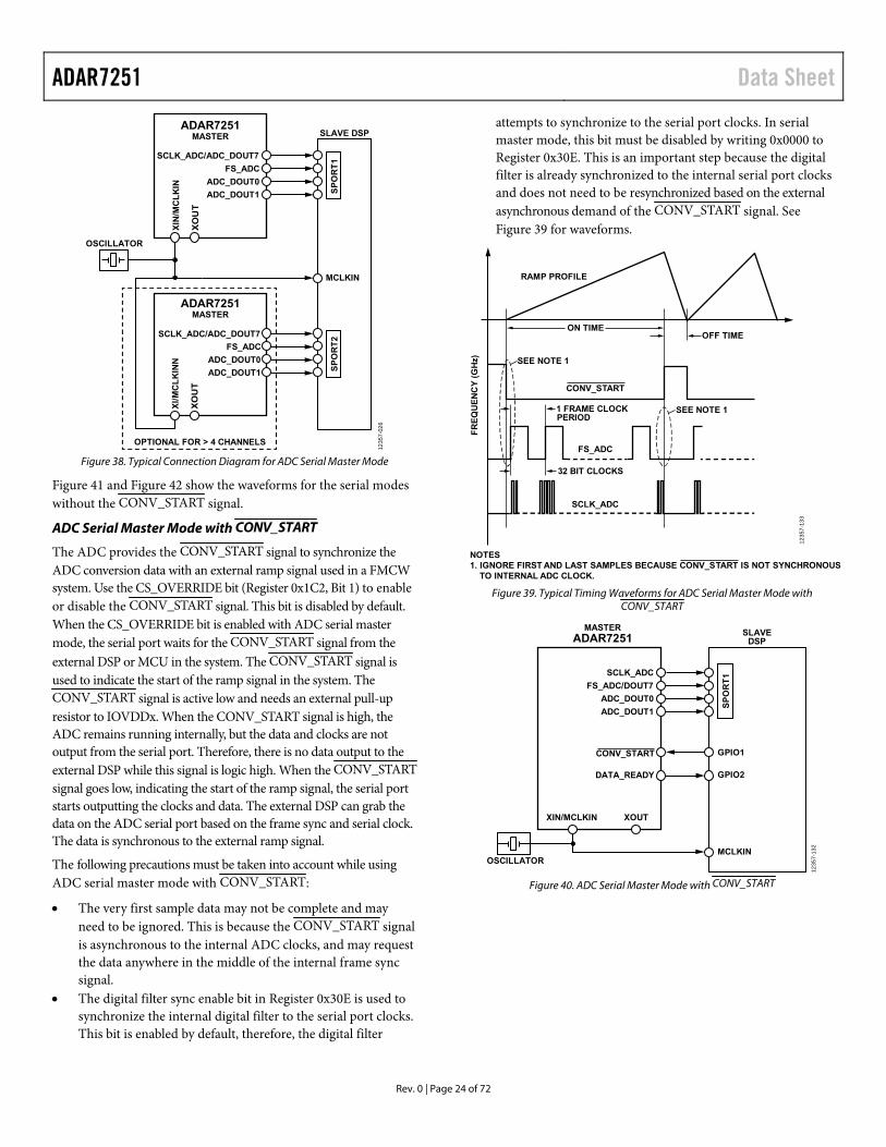
ADC Serial Master Mode with CONV_START
The ADC provides the CONV_START signal to synchronize the ADC conversion data with an external ramp signal used in a FMCW system. Use the CS_OVERRIDE bit (Register 0x1C2, Bit 1) to enable or disable the CONV_START signal. This bit is disabled by default. When the CS_OVERRIDE bit is enabled with ADC serial master mode, the serial port waits for the CONV_START signal from the external DSP or MCU in the system. The CONV_START signal is used to indicate the start of the ramp signal in the system. The CONV_START signal is active low and needs an external pull-up resistor to IOVDDx. When the CONV_START signal is high, the ADC remains running internally, but the data and clocks are not output from the serial port. Therefore, there is no data output to the external DSP while this signal is logic high. When the CONV_START signal goes low, indicating the start of the ramp signal, the serial port starts outputting the clocks and data. The external DSP can grab the data on the ADC serial port based on the frame sync and serial clock. The data is synchronous to the external ramp signal.
The following precautions must be taken into account while using ADC serial master mode with CONV_START:
The very first sample data may not be complete and may need to be ignored. This is because the CONV_START signal is asynchronous to the internal ADC clocks, and may request the data anywhere in the middle of the internal frame sync signal.
The digital filter sync enable bit in Register 0x30E is used to synchronize the internal digital filter to the serial port clocks. This bit is enabled by default, therefore, the digital filter
attempts to synchronize to the serial port clocks. In serial master mode, this bit must be disabled by writing 0x0000 to Register 0x30E. This is an important step because the digital filter is already synchronized to the internal serial port clocks and does not need to be resynchronized based on the external asynchronous demand of the CONV_START signal. See Figure 39 for waveforms.
ON TIME
RAMP PROFILE
CONV_START
FS_ADC
SCLK_ADC
SEE NOTE 1
NOTES1. IGNORE FIRST AND LAST SAMPLES BECAUSE CONV_START IS NOT SYNCHRONOUS
TO INTERNAL ADC CLOCK.
FR
EQ
UE
NC
Y (
GH
z)
OFF TIME
1 FRAME CLOCKPERIOD
32 BIT CLOCKS
SEE NOTE 1
123
57-1
33
Figure 39. Typical Timing Waveforms for ADC Serial Master Mode with
CONV_START
MASTERADAR7251
SLAVEDSP
XIN/MCLKIN
OSCILLATOR
XOUT
GPIO1
GPIO2
CONV_START
DATA_READY
1235
7-1
32
SP
OR
T1
MCLKIN
SCLK_ADC
FS_ADC/DOUT7
ADC_DOUT0
ADC_DOUT1
Figure 40. ADC Serial Master Mode with CONV_START

Data Sheet ADAR7251
Rev. 0 | Page 25 of 72
0 3115SCLK_ADC
FS_ADC
ADC_DOUT0
ADC_DOUT1
CHANNEL 2
CHANNEL 3 CHANNEL 4
CHANNEL 1
12
35
7-0
27
Figure 41. Serial Mode, Two Channels per the ADC_DOUTx Pins
0SCLK_ADC
FS_ADC
ADC_DOUT0
3115
CHANNEL 1 CHANNEL 2 CHANNEL 3 CHANNEL 4
63
123
57-0
28
Figure 42. Serial Mode, 4 Channels per the ADC_DOUTx Pins
SCLK_ADC
FS_ADC/ADC_DOUT7
ADC_DOUT0 MASTERDSP
MASTERSPI
ADAR7251SLAVE
ADAR7251SLAVE
XIN
/MC
LK
IN
SP
I_S
S
XIN
/MC
LK
IN
SP
I_S
S
SP
OR
T1
OPTIONAL FOR > 4 CHANNELS
FCLK = 16MHz TO 54MHz
ADC_DOUT1
SCLK_ADC
FS_ADC/ADC_DOUT7
ADC_DOUT0
ADC_DOUT1
SP
I_S
CL
KS
PI_
SC
LK
SP
I_M
OS
IS
PI_
MO
SI
SP
I_M
ISO
SPI_MISO
SPI_MOSI
SPI_SCLK
SPI_SS1SPI_SS2
MCLKOUT
SP
I_M
ISO
123
57-0
29
Figure 43. Typical Connection Diagram for ADC Serial Slave Mode
ADC Serial Slave
Figure 43 shows the typical connection diagram for ADC serial slave mode. In this mode, the directions of the frame sync and bit clock pins change. Both pins are inputs and must be provided with bit clock and frame sync signals via an external DSP. The ADC_DOUT0 and ADC_DOUT1 pins are always used as outputs. The data format is fixed as MSB first. The ADC must be provided with master clock from the DSP to synchronize the ports.
ADC PPI (Byte Wide Mode)
ADC PPI mode is parallel byte wide mode and, in this mode, the device is always master. In this mode, the ADC outputs the bit clock and data. Provide the ADC port with a conversion start
signal (CONV_START) if selected. This initiates the conversion process. When the ADC is ready with conversion data, it pulls the DATA_READY pin high to indicate the data ready status to the DSP. The ADC then provides the bit clock, SCLK_ADC. The data is available on the rising edge of the bit clock. The maximum sample rate supported is 3.6 MHz in this mode. The data is available on the ADC_DOUT0 through ADC_DOUT7 pins, one byte at a time. The ADC data is twos complement, 16-bit binary, but the 16-bit data is split into two bytes: a higher byte and a lower byte (each is 8 bits wide). The higher byte is output first, and is followed by the lower byte. The bit clock (SCLK_ADC) rate depends on the sample rate setting. See Table 14 for available options. Note that in the PPI mode, the FS_ADC output is not

ADAR7251 Data Sheet
Rev. 0 | Page 26 of 72
available. This mode may be useful if the DSP port cannot support the 38.4 MHz data rate. The data rate is less than that of the serial port; however, it uses more pins for data.
Table 14. Bit Clock Rate Options for ADC PPI Byte Wide Mode Number of Channels
FS_ADC (MHz)
SCLK_ADC (MHz) Data Output Pins
2 1.2 4.8 ADC_DOUT0 through ADC_DOUT7
4 1.2 9.6 ADC_DOUT0 through ADC_DOUT7
2 1.8 7.2 ADC_DOUT0 through ADC_DOUT7
4 1.8 14.4 ADC_DOUT0 through ADC_DOUT7
The other sample rates supported are 300 kHz, 600 kHz, 900 kHz, 2.4 MHz, and 3.6 MHz. The highest serial clock supported is 57.6 MHz. However, as the sample rate increases beyond 1.2 MHz, the ADC resolution decreases. At the highest sample rate of 3.6 MHz, the ADC resolution is limited to 11 bits.
Figure 44 shows the typical connections diagram for ADC PPI master mode.
Figure 45 and Figure 46 show waveforms for PPI 2-channel and PPI 4-channel mode.
ADC_DOUT0TO
ADC_DOUT7
ADC_DOUT0TOADC_DOUT7
MASTERADAR7251
SLAVEDSP
XIN XOUT MCLKOUT
SCLK
GPIO1
GPIO2
CONV_START
DATA_READY
SCLK_ADC
12
357
-030
Figure 44. Typical Connection Diagram for ADC PPI Master Mode
B15
CHANNEL 1
0 1
CHANNEL 2
2 3
B14
B13
B12
B11
B10
B9
B8
B7
B6 B14 B6 B14 B6 B14 B6 B14 B6 B14 B6 B14 B6 B14 B6
B5 B13 B5 B13 B5 B13 B5 B13 B5 B13 B5 B13 B5 B13 B5
B4 B12 B4 B12 B4 B12 B4 B12 B4 B12 B4 B12 B4 B12 B4
B3 B11 B3 B11 B3 B11 B3 B11 B3 B11 B3 B11 B3 B11 B3
B2 B10 B2 B10 B2 B10 B2 B10 B2 B10 B2 B10 B2 B10 B2
B1 B9 B1 B9 B1 B9 B1 B9 B1 B9 B1 B9 B1 B9 B1
B0 B8 B0 B8 B0 B8 B0 B8 B0 B8 B0 B8 B0 B8 B0
B7B15 B15 B7B7B15 B15 B7B7B15 B15 B7B7B15
CHANNEL 1 CHANNEL 2 CHANNEL 1 CHANNEL 2 CHANNEL 1 CHANNEL 2
CONV_START
DATA_READY
SCLK_ADC
ADC_DOUT7
ADC_DOUT6
ADC_DOUT5
ADC_DOUT4
ADC_DOUT3
ADC_DOUT2
ADC_DOUT1
ADC_DOUT0
123
57-
031
Figure 45. PPI, 2-Channel
Data Sheet ADAR7251
Rev. 0 | Page 27 of 72
B15
CHANNEL 1
0 1
CHANNEL 2
2 3
B14
B13
B12
B11
B10
B9
B8
B7
B6 B14 B6 B14 B6 B14 B6 B14 B6 B14 B6 B14 B6 B14 B6
B5 B13 B5 B13 B5 B13 B5 B13 B5 B13 B5 B13 B5 B13 B5
B4 B12 B4 B12 B4 B12 B4 B12 B4 B12 B4 B12 B4 B12 B4
B3 B11 B3 B11 B3 B11 B3 B11 B3 B11 B3 B11 B3 B11 B3
B2 B10 B2 B10 B2 B10 B2 B10 B2 B10 B2 B10 B2 B10 B2
B1 B9 B1 B9 B1 B9 B1 B9 B1 B9 B1 B9 B1 B9 B1
B0 B8 B0 B8 B0 B8 B0 B8 B0 B8 B0 B8 B0 B8 B0
B7B15 B15 B7B7B15 B15 B7B7B15 B15 B7B7B15
CHANNEL 3 CHANNEL 4 CHANNEL 1 CHANNEL 2 CHANNEL 3 CHANNEL 4
DATA_READY
SCLK_ADC
ADC_DOUT7
ADC_DOUT6
ADC_DOUT5
ADC_DOUT4
ADC_DOUT3
ADC_DOUT2
ADC_DOUT1
ADC_DOUT0
123
57-
03
2
CONV_START
Figure 46. PPI, 4-Channel
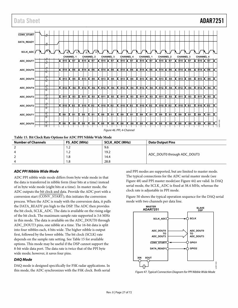
Table 15. Bit Clock Rate Options for ADC PPI Nibble Wide Mode Number of Channels FS_ADC (MHz) SCLK_ADC (MHz) Data Output Pins 2 1.2 9.6
ADC_DOUT0 through ADC_DOUT3 4 1.2 19.2 2 1.8 14.4 4 1.8 28.8
ADC PPI Nibble Wide Mode
ADC PPI nibble wide mode differs from byte wide mode in that the data is transferred in nibble form (four bits at a time) instead of in byte wide mode (eight bits at a time). In master mode, the ADC outputs the bit clock and data. Provide the ADC port with a conversion start (CONV_START); this initiates the conversion process. When the ADC is ready with the conversion data, it pulls the DATA_READY pin high to the DSP. The ADC then provides the bit clock, SCLK_ADC. The data is available on the rising edge of the bit clock. The maximum sample rate supported is 3.6 MHz in this mode. The data is available on the ADC_DOUT0 through ADC_DOUT3 pins, one nibble at a time. The 16-bit data is split into four nibbles each, 4 bits wide. The higher nibble is output first, followed by the lower nibble. The bit clock (SCLK) rate depends on the sample rate setting. See Table 15 for available options. This mode may be useful if the DSP cannot support the 8-bit wide data port. The data rate is twice that of the PPI byte wide mode; however, it saves four pins.
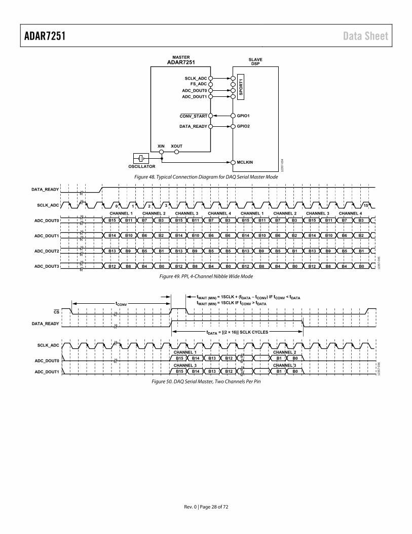
DAQ Mode
DAQ mode is designed specifically for FSK radar applications. In this mode, the ADC synchronizes with the FSK clock. Both serial
and PPI modes are supported, but are limited to master mode. The typical connections for the ADC serial master mode (see Figure 48) and PPI master mode(see Figure 44) are valid. In DAQ serial mode, the SCLK_ADC is fixed at 38.4 MHz, whereas the clock rate is adjustable in PPI mode.
Figure 50 shows the typical operation sequence for the DAQ serial mode with two channels per data line.
ADC_DOUT0TO
ADC_DOUT3
ADC_DOUT0TOADC_DOUT3
MASTERADAR7251
SLAVEDSP
XIN XOUT
SCLK
GPIO1
GPIO2
CONV_START
DATA_READY
SCLK_ADC1
235
7-0
33
Figure 47. Typical Connection Diagram for PPI Nibble Wide Mode
ADAR7251 Data Sheet
Rev. 0 | Page 28 of 72
MASTERADAR7251
SLAVEDSP
XIN
OSCILLATOR
XOUT
GPIO1
GPIO2
CONV_START
DATA_READY
123
57
-034
SP
OR
T1
MCLKIN
SCLK_ADCFS_ADC
ADC_DOUT0
ADC_DOUT1
Figure 48. Typical Connection Diagram for DAQ Serial Master Mode
B15
CHANNEL 1
0 1
CHANNEL 2
2 3 15
B14
B13
B12
B11
B10 B6 B2 B14 B10 B6 B6 B14 B10 B6 B2 B14 B10 B6 B2
B9 B5 B1 B13 B9 B5 B5 B13 B9 B5 B1 B13 B9 B5 B1
B8 B4 B0 B12 B8 B4 B0 B12 B8 B4 B0 B12 B8 B4 B0
B3B7 B7 B3B11B15 B7 B3B11B15 B7 B3B11B15
CHANNEL 3 CHANNEL 4 CHANNEL 1 CHANNEL 2 CHANNEL 3 CHANNEL 4
DATA_READY
SCLK_ADC
ADC_DOUT0
ADC_DOUT1
ADC_DOUT2
ADC_DOUT3
1235
7-03
5
Figure 49. PPI, 4-Channel Nibble Wide Mode
tCONV
tWAIT (MIN) = 1SCLK + (tDATA – tCONV) IF tCONV < tDATA
tDATA = [(2 × 16)] SCLK CYCLES
tWAIT (MIN) = 1SCLK IF tCONV > tDATA
12
35
7-0
36
DATA_READY
CS
SCLK_ADC
ADC_DOUT0
ADC_DOUT1
B15
CHANNEL 1
B15
B15 B14
B14
B13
B13
B12
B12
CHANNEL 3
B15
CHANNEL 2
B1
B1 B0
B0
CHANNEL 3
Figure 50. DAQ Serial Master, Two Channels Per Pin
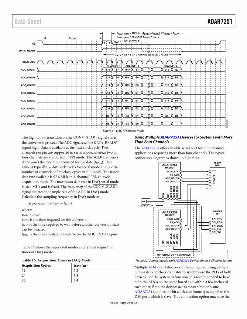
Data Sheet ADAR7251
Rev. 0 | Page 29 of 72
tCONV
tWAIT (MIN) = 1SCLK + (tDATA – tCONV) IF tCONV < tDATA
tWAIT (MIN) = 1SCLK IF tCONV > tDATA
123
57
-037
DATA_READY
CS
SCLK_ADC
ADC_DOUT7
ADC_DOUT6
ADC_DOUT5
ADC_DOUT4
ADC_DOUT3
ADC_DOUT2
ADC_DOUT1
ADC_DOUT0
B15
CHANNEL 1 CHANNEL 2
B14
B7 B15 B7
B6
CHANNEL 4
B15 B7
B13 B5
B12 B4
B11 B3
B10 B2
B9 B1
B8 B0
B14 B6
B13 B5
B12 B4
B11 B3
B10 B2
B9 B1
B8 B0 B8 B0
B14 B6
B13 B5
B12 B4
B11 B3
B10 B2
B9 B1
tWAIT = 1 SCLK CYCLE
tDATA = [(2 × # OF CHANNELS)] SCLK CYCLES
Figure 51. DAQ PPI Master Mode
The high to low transition on the CONV_START signal starts the conversion process. The ADC signals set the DATA_READY signal high. Data is available at the next clock cycle. Two channels per pin are supported in serial mode, whereas two or four channels are supported in PPI mode. The SCLK frequency determines the total time required for the data (tDATA). This value is typically 32-bit clock cycles for serial mode and (2× the number of channels) of bit clock cycles in PPI mode. The fastest data rate available is 57.6 MHz in 2-channel, PPI, 16-cycle acquisition mode. The maximum data rate in DAQ serial mode is 38.4 MHz and is fixed. The frequency of the CONV_STARTsignal dictates the sample rate of the ADC in DAQ mode. Calculate the sampling frequency in DAQ mode as
fS DAQ_MODE = 1/(tCONV + tWAIT)
where: tDATA < tCONV. tCONV is the time required for the conversion. tWAIT is the time required to wait before another conversion start can be initiated. tDATA is the time the data is available on the ADC_DOUTx pins.
Table 16 shows the supported modes and typical acquisition times in DAQ mode.
Table 16. Acquisition Times in DAQ Mode Acquisition Cycles tCONV (μs) 16 1.2 24 1.8 32 2.4
Using Multiple ADAR7251 Devices for Systems with More Than Four Channels
The ADAR7251 offers flexible serial port for multichannel applications requiring more than four channels. The typical connection diagram is shown in Figure 52.
SCLK_ADC
FS_ADC
ADC_DOUT0
SLAVEDSP
MASTERSPI
ADAR7251MASTER
ADAR7251MASTER
XIN
SS
XIN
SS
SP
OR
T1
OPTIONAL FOR > 4 CHANNELS
ADC_DOUT1
SCLK_ADC
FS_ADC
ADC_DOUT0
ADC_DOUT1
SP
I_S
CL
KS
PI_
SC
LK
SP
I_M
OS
IS
PI_
MO
SI
SP
I_M
ISO
SPI_MISO
SPI_MOSI
SPI_SCLK
SPI_SS1SPI_SS2
SP
I_M
ISO
12
35
7-0
38
OSCILLATOR
Figure 52. Connecting Multiple ADAR7251 Devices for an 8-Channel System
Multiple ADAR7251 devices can be configured using a single SPI master and clock oscillator to synchronize the PLLs of both devices. For the system to function, it is recommended to have both the ADCs on the same board and within a few inches of each other. Both the devices act as master, but only one ADAR7251 supplies the bit clock and frame sync signal to the DSP port, which is slave. This connection option may save the
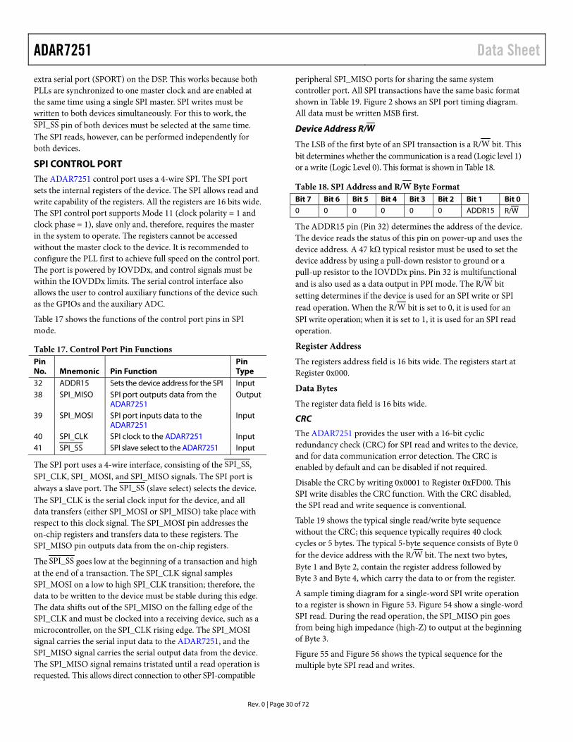
ADAR7251 Data Sheet
Rev. 0 | Page 30 of 72
extra serial port (SPORT) on the DSP. This works because both PLLs are synchronized to one master clock and are enabled at the same time using a single SPI master. SPI writes must be written to both devices simultaneously. For this to work, the SPI_SS pin of both devices must be selected at the same time. The SPI reads, however, can be performed independently for both devices.
SPI CONTROL PORT The ADAR7251 control port uses a 4-wire SPI. The SPI port sets the internal registers of the device. The SPI allows read and write capability of the registers. All the registers are 16 bits wide. The SPI control port supports Mode 11 (clock polarity = 1 and clock phase = 1), slave only and, therefore, requires the master in the system to operate. The registers cannot be accessed without the master clock to the device. It is recommended to configure the PLL first to achieve full speed on the control port. The port is powered by IOVDDx, and control signals must be within the IOVDDx limits. The serial control interface also allows the user to control auxiliary functions of the device such as the GPIOs and the auxiliary ADC.
Table 17 shows the functions of the control port pins in SPI mode.
Table 17. Control Port Pin Functions Pin No. Mnemonic Pin Function
Pin Type
32 ADDR15 Sets the device address for the SPI Input 38 SPI_MISO SPI port outputs data from the
ADAR7251 Output
39 SPI_MOSI SPI port inputs data to the ADAR7251
Input
40 SPI_CLK SPI clock to the ADAR7251 Input 41 SPI_SS SPI slave select to the ADAR7251 Input
The SPI port uses a 4-wire interface, consisting of the SPI_SS, SPI_CLK, SPI_ MOSI, and SPI_MISO signals. The SPI port is always a slave port. The SPI_SS (slave select) selects the device. The SPI_CLK is the serial clock input for the device, and all data transfers (either SPI_MOSI or SPI_MISO) take place with respect to this clock signal. The SPI_MOSI pin addresses the on-chip registers and transfers data to these registers. The SPI_MISO pin outputs data from the on-chip registers.
The SPI_SS goes low at the beginning of a transaction and high at the end of a transaction. The SPI_CLK signal samples SPI_MOSI on a low to high SPI_CLK transition; therefore, the data to be written to the device must be stable during this edge. The data shifts out of the SPI_MISO on the falling edge of the SPI_CLK and must be clocked into a receiving device, such as a microcontroller, on the SPI_CLK rising edge. The SPI_MOSI signal carries the serial input data to the ADAR7251, and the SPI_MISO signal carries the serial output data from the device. The SPI_MISO signal remains tristated until a read operation is requested. This allows direct connection to other SPI-compatible
peripheral SPI_MISO ports for sharing the same system controller port. All SPI transactions have the same basic format shown in Table 19. Figure 2 shows an SPI port timing diagram. All data must be written MSB first.
Device Address R/W
The LSB of the first byte of an SPI transaction is a R/W bit. This bit determines whether the communication is a read (Logic level 1) or a write (Logic Level 0). This format is shown in Table 18.
Table 18. SPI Address and R/W Byte Format Bit 7 Bit 6 Bit 5 Bit 4 Bit 3 Bit 2 Bit 1 Bit 0 0 0 0 0 0 0 ADDR15 R/W
The ADDR15 pin (Pin 32) determines the address of the device. The device reads the status of this pin on power-up and uses the device address. A 47 kΩ typical resistor must be used to set the device address by using a pull-down resistor to ground or a pull-up resistor to the IOVDDx pins. Pin 32 is multifunctional and is also used as a data output in PPI mode. The R/W bit setting determines if the device is used for an SPI write or SPI read operation. When the R/W bit is set to 0, it is used for an SPI write operation; when it is set to 1, it is used for an SPI read operation.
Register Address
The registers address field is 16 bits wide. The registers start at Register 0x000.
Data Bytes
The register data field is 16 bits wide.
CRC
The ADAR7251 provides the user with a 16-bit cyclic redundancy check (CRC) for SPI read and writes to the device, and for data communication error detection. The CRC is enabled by default and can be disabled if not required.
Disable the CRC by writing 0x0001 to Register 0xFD00. This SPI write disables the CRC function. With the CRC disabled, the SPI read and write sequence is conventional.
Table 19 shows the typical single read/write byte sequence without the CRC; this sequence typically requires 40 clock cycles or 5 bytes. The typical 5-byte sequence consists of Byte 0 for the device address with the R/W bit. The next two bytes, Byte 1 and Byte 2, contain the register address followed by Byte 3 and Byte 4, which carry the data to or from the register.
A sample timing diagram for a single-word SPI write operation to a register is shown in Figure 53. Figure 54 show a single-word SPI read. During the read operation, the SPI_MISO pin goes from being high impedance (high-Z) to output at the beginning of Byte 3.
Figure 55 and Figure 56 shows the typical sequence for the multiple byte SPI read and writes.
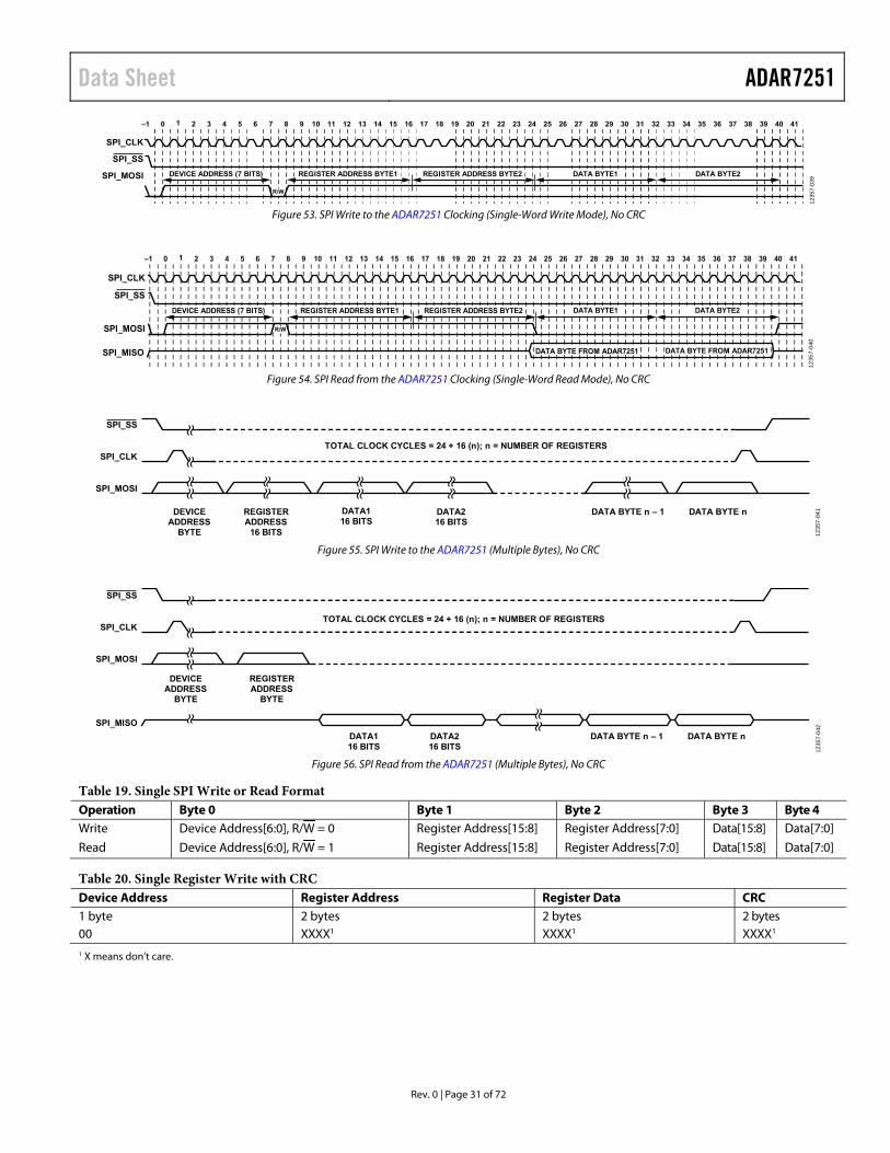
Data Sheet ADAR7251
Rev. 0 | Page 31 of 72
–1 0 1 2 3 4 5 6 7 8 9 10 11 12 13 14 15 16 17 18 19 20 21 22 23 24 25 26 27 28 29 30 31 32 33 34 35 36 37 38 39 40 41
R/W
DEVICE ADDRESS (7 BITS) REGISTER ADDRESS BYTE1 REGISTER ADDRESS BYTE2 DATA BYTE1 DATA BYTE2
SPI_CLK
SPI_SS
SPI_MOSI
123
57-
039
Figure 53. SPI Write to the ADAR7251 Clocking (Single-Word Write Mode), No CRC
–1 0 1 2 3 4 5 6 7 8 9 10 11 12 13 14 15 16 17 18 19 20 21 22 23 24 25 26 27 28 29 30 31 32 33 34 35 36 37 38 39 40 41
R/W
DEVICE ADDRESS (7 BITS) REGISTER ADDRESS BYTE1 REGISTER ADDRESS BYTE2 DATA BYTE1 DATA BYTE2
SPI_CLK
SPI_SS
SPI_MOSI
12
35
7-0
40
DATA BYTE FROM ADAR7251 DATA BYTE FROM ADAR7251SPI_MISO
Figure 54. SPI Read from the ADAR7251 Clocking (Single-Word Read Mode), No CRC
TOTAL CLOCK CYCLES = 24 + 16 (n); n = NUMBER OF REGISTERS
DATA116 BITS
DATA216 BITS
DEVICEADDRESS
BYTE
REGISTERADDRESS
16 BITS
DATA BYTE n – 1 DATA BYTE n
SPI_SS
SPI_CLK
SPI_MOSI
123
57
-04
1
Figure 55. SPI Write to the ADAR7251 (Multiple Bytes), No CRC
DEVICEADDRESS
BYTE
REGISTERADDRESS
BYTE
DATA216 BITS
DATA116 BITS
DATA BYTE n – 1 DATA BYTE n
SPI_SS
SPI_CLK
SPI_MOSI
SPI_MISO
123
57-0
42
TOTAL CLOCK CYCLES = 24 + 16 (n); n = NUMBER OF REGISTERS
Figure 56. SPI Read from the ADAR7251 (Multiple Bytes), No CRC
Table 19. Single SPI Write or Read Format Operation Byte 0 Byte 1 Byte 2 Byte 3 Byte 4 Write Device Address[6:0], R/W = 0 Register Address[15:8] Register Address[7:0] Data[15:8] Data[7:0]
Read Device Address[6:0], R/W = 1 Register Address[15:8] Register Address[7:0] Data[15:8] Data[7:0]
Table 20. Single Register Write with CRC Device Address Register Address Register Data CRC 1 byte 2 bytes 2 bytes 2 bytes 00 XXXX1 XXXX1 XXXX1 1 X means don’t care.
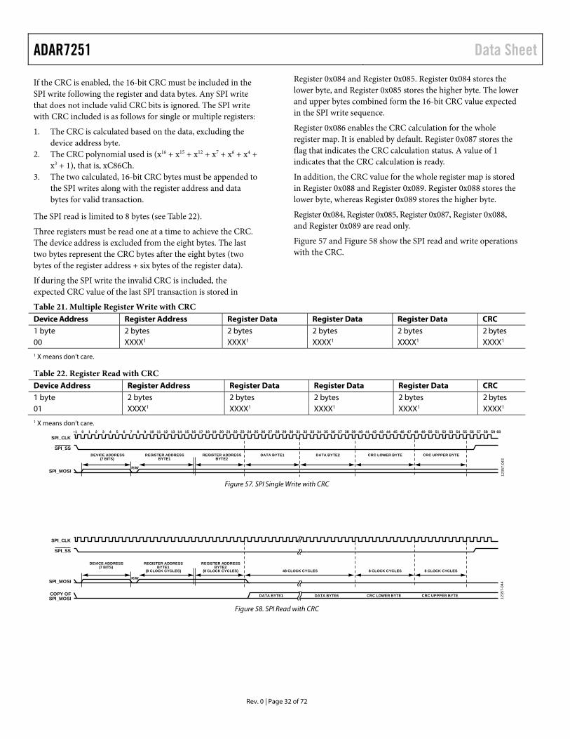
ADAR7251 Data Sheet
Rev. 0 | Page 32 of 72
If the CRC is enabled, the 16-bit CRC must be included in the SPI write following the register and data bytes. Any SPI write that does not include valid CRC bits is ignored. The SPI write with CRC included is as follows for single or multiple registers:
1. The CRC is calculated based on the data, excluding the device address byte.
2. The CRC polynomial used is (x16 + x15 + x12 + x7 + x6 + x4 + x3 + 1), that is, xC86Ch.
3. The two calculated, 16-bit CRC bytes must be appended to the SPI writes along with the register address and data bytes for valid transaction.
The SPI read is limited to 8 bytes (see Table 22).
Three registers must be read one at a time to achieve the CRC. The device address is excluded from the eight bytes. The last two bytes represent the CRC bytes after the eight bytes (two bytes of the register address + six bytes of the register data).
If during the SPI write the invalid CRC is included, the expected CRC value of the last SPI transaction is stored in
Register 0x084 and Register 0x085. Register 0x084 stores the lower byte, and Register 0x085 stores the higher byte. The lower and upper bytes combined form the 16-bit CRC value expected in the SPI write sequence.
Register 0x086 enables the CRC calculation for the whole register map. It is enabled by default. Register 0x087 stores the flag that indicates the CRC calculation status. A value of 1 indicates that the CRC calculation is ready.
In addition, the CRC value for the whole register map is stored in Register 0x088 and Register 0x089. Register 0x088 stores the lower byte, whereas Register 0x089 stores the higher byte.
Register 0x084, Register 0x085, Register 0x087, Register 0x088, and Register 0x089 are read only.
Figure 57 and Figure 58 show the SPI read and write operations with the CRC.
Table 21. Multiple Register Write with CRC Device Address Register Address Register Data Register Data Register Data CRC 1 byte 2 bytes 2 bytes 2 bytes 2 bytes 2 bytes 00 XXXX1 XXXX1 XXXX1 XXXX1 XXXX1 1 X means don’t care.
Table 22. Register Read with CRC Device Address Register Address Register Data Register Data Register Data CRC 1 byte 2 bytes 2 bytes 2 bytes 2 bytes 2 bytes 01 XXXX1 XXXX1 XXXX1 XXXX1 XXXX1 1 X means don’t care.
–1 0 1 2 3 4 5 6 7 8 9 10 11 12 13 14 15 16 17 18 19 20 21 22 23 24 25 26 27 28 29 30 31 32 33 34 35 36 37 38 39 40 41 42 43 44 45 46 47 48 49 50 51 52 53 54 55 56 57 58 59 60
R/W
DEVICE ADDRESS(7 BITS)
REGISTER ADDRESSBYTE1
REGISTER ADDRESSBYTE2
DATA BYTE1 DATA BYTE2 CRC LOWER BYTE CRC UPPPER BYTE
SPI_CLK
SPI_SS
SPI_MOSI
123
57-0
43
Figure 57. SPI Single Write with CRC
R/W
DEVICE ADDRESS(7 BITS)
REGISTER ADDRESSBYTE1
(8 CLOCK CYCLES)
REGISTER ADDRESSBYTE2
(8 CLOCK CYCLES)
DATA BYTE1 DATA BYTE6 CRC LOWER BYTE CRC UPPPER BYTE
SPI_CLK
SPI_SS
SPI_MOSI
COPY OFSPI_MOSI 1
2357
-04
4
8 CLOCK CYCLES48 CLOCK CYCLES 8 CLOCK CYCLES
Figure 58. SPI Read with CRC
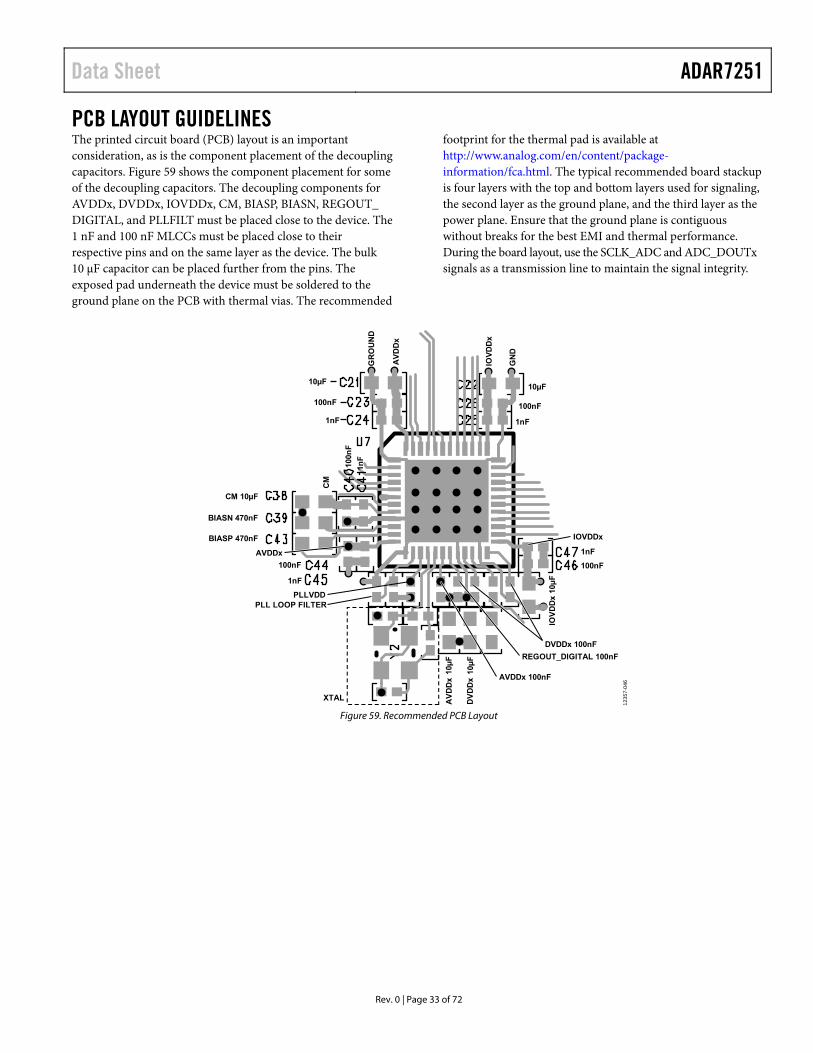
Data Sheet ADAR7251
Rev. 0 | Page 33 of 72
PCB LAYOUT GUIDELINES The printed circuit board (PCB) layout is an important consideration, as is the component placement of the decoupling capacitors. Figure 59 shows the component placement for some of the decoupling capacitors. The decoupling components for AVDDx, DVDDx, IOVDDx, CM, BIASP, BIASN, REGOUT_ DIGITAL, and PLLFILT must be placed close to the device. The 1 nF and 100 nF MLCCs must be placed close to their respective pins and on the same layer as the device. The bulk 10 μF capacitor can be placed further from the pins. The exposed pad underneath the device must be soldered to the ground plane on the PCB with thermal vias. The recommended
footprint for the thermal pad is available at http://www.analog.com/en/content/package-information/fca.html. The typical recommended board stackup is four layers with the top and bottom layers used for signaling, the second layer as the ground plane, and the third layer as the power plane. Ensure that the ground plane is contiguous without breaks for the best EMI and thermal performance. During the board layout, use the SCLK_ADC and ADC_DOUTx signals as a transmission line to maintain the signal integrity.
123
57-
046
AV
DD
x
GR
OU
ND
1nF
100nF
10µF
IOV
DD
x
GN
D
IOVDDx
DVDDx 100nF
CM
1nF
100nF
PLL LOOP FILTER
XTAL
AVDDx 1nF
100nF
1nF
100nF
10µF
BIASN 470nF
BIASP 470nF
REGOUT_DIGITAL 100nF
PLLVDD
10µ
F
10µ
F
AV
DD
x
DV
DD
x
IOV
DD
x 10
µF
CM 10µF
1nF
100n
F
AVDDx 100nF
Figure 59. Recommended PCB Layout
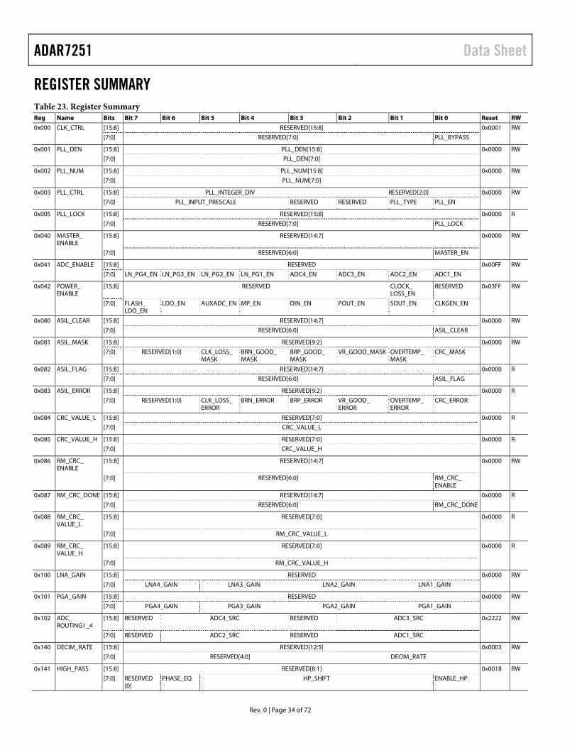
ADAR7251 Data Sheet
Rev. 0 | Page 34 of 72
REGISTER SUMMARY Table 23. Register Summary Reg Name Bits Bit 7 Bit 6 Bit 5 Bit 4 Bit 3 Bit 2 Bit 1 Bit 0 Reset RW
0x000 CLK_CTRL [15:8] RESERVED[15:8] 0x0001 RW
[7:0] RESERVED[7:0] PLL_BYPASS 0x001 PLL_DEN [15:8] PLL_DEN[15:8] 0x0000 RW
[7:0] PLL_DEN[7:0] 0x002 PLL_NUM [15:8] PLL_NUM[15:8] 0x0000 RW
[7:0] PLL_NUM[7:0] 0x003 PLL_CTRL [15:8] PLL_INTEGER_DIV RESERVED[2:0] 0x0000 RW
[7:0] PLL_INPUT_PRESCALE RESERVED RESERVED PLL_TYPE PLL_EN 0x005 PLL_LOCK [15:8] RESERVED[15:8] 0x0000 R
[7:0] RESERVED[7:0] PLL_LOCK 0x040 MASTER_
ENABLE [15:8] RESERVED[14:7] 0x0000 RW
[7:0] RESERVED[6:0] MASTER_EN 0x041 ADC_ENABLE [15:8] RESERVED 0x00FF RW
[7:0] LN_PG4_EN LN_PG3_EN LN_PG2_EN LN_PG1_EN ADC4_EN ADC3_EN ADC2_EN ADC1_EN 0x042 POWER_
ENABLE [15:8] RESERVED CLOCK_
LOSS_EN RESERVED 0x03FF RW
[7:0] FLASH_ LDO_EN
LDO_EN AUXADC_EN MP_EN DIN_EN POUT_EN SOUT_EN CLKGEN_EN
0x080 ASIL_CLEAR [15:8] RESERVED[14:7] 0x0000 RW
[7:0] RESERVED[6:0] ASIL_CLEAR 0x081 ASIL_MASK [15:8] RESERVED[9:2] 0x0000 RW
[7:0] RESERVED[1:0] CLK_LOSS_ MASK
BRN_GOOD_ MASK
BRP_GOOD_ MASK
VR_GOOD_MASK OVERTEMP_ MASK
CRC_MASK
0x082 ASIL_FLAG [15:8] RESERVED[14:7] 0x0000 R
[7:0] RESERVED[6:0] ASIL_FLAG 0x083 ASIL_ERROR [15:8] RESERVED[9:2] 0x0000 R
[7:0] RESERVED[1:0] CLK_LOSS_ ERROR
BRN_ERROR BRP_ERROR VR_GOOD_ ERROR
OVERTEMP_ ERROR
CRC_ERROR
0x084 CRC_VALUE_L [15:8] RESERVED[7:0] 0x0000 R
[7:0] CRC_VALUE_L 0x085 CRC_VALUE_H [15:8] RESERVED[7:0] 0x0000 R
[7:0] CRC_VALUE_H 0x086 RM_CRC_
ENABLE [15:8] RESERVED[14:7] 0x0000 RW
[7:0] RESERVED[6:0] RM_CRC_ ENABLE
0x087 RM_CRC_DONE [15:8] RESERVED[14:7] 0x0000 R
[7:0] RESERVED[6:0] RM_CRC_DONE 0x088 RM_CRC_
VALUE_L [15:8] RESERVED[7:0] 0x0000 R
[7:0] RM_CRC_VALUE_L 0x089 RM_CRC_
VALUE_H [15:8] RESERVED[7:0] 0x0000 R
[7:0] RM_CRC_VALUE_H 0x100 LNA_GAIN [15:8] RESERVED 0x0000 RW
[7:0] LNA4_GAIN LNA3_GAIN LNA2_GAIN LNA1_GAIN 0x101 PGA_GAIN [15:8] RESERVED 0x0000 RW
[7:0] PGA4_GAIN PGA3_GAIN PGA2_GAIN PGA1_GAIN 0x102 ADC_
ROUTING1_4 [15:8] RESERVED ADC4_SRC RESERVED ADC3_SRC 0x2222 RW
[7:0] RESERVED ADC2_SRC RESERVED ADC1_SRC 0x140 DECIM_RATE [15:8] RESERVED[12:5] 0x0003 RW
[7:0] RESERVED[4:0] DECIM_RATE 0x141 HIGH_PASS [15:8] RESERVED[8:1] 0x0018 RW
[7:0] RESERVED [0]
PHASE_EQ HP_SHIFT ENABLE_HP
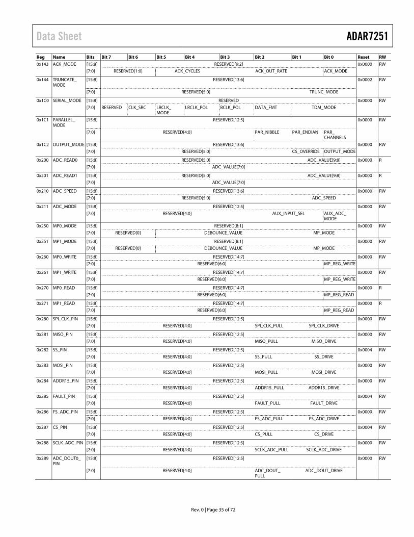
Data Sheet ADAR7251
Rev. 0 | Page 35 of 72
Reg Name Bits Bit 7 Bit 6 Bit 5 Bit 4 Bit 3 Bit 2 Bit 1 Bit 0 Reset RW
0x143 ACK_MODE [15:8] RESERVED[9:2] 0x0000 RW
[7:0] RESERVED[1:0] ACK_CYCLES ACK_OUT_RATE ACK_MODE 0x144 TRUNCATE_
MODE [15:8] RESERVED[13:6] 0x0002 RW
[7:0] RESERVED[5:0] TRUNC_MODE 0x1C0 SERIAL_MODE [15:8] RESERVED 0x0000 RW
[7:0] RESERVED CLK_SRC LRCLK_ MODE
LRCLK_POL BCLK_POL DATA_FMT TDM_MODE
0x1C1 PARALLEL_ MODE
[15:8] RESERVED[12:5] 0x0000 RW
[7:0] RESERVED[4:0] PAR_NIBBLE PAR_ENDIAN PAR_ CHANNELS
0x1C2 OUTPUT_MODE [15:8] RESERVED[13:6] 0x0000 RW
[7:0] RESERVED[5:0] CS_OVERRIDE OUTPUT_MODE 0x200 ADC_READ0 [15:8] RESERVED[5:0] ADC_VALUE[9:8] 0x0000 R
[7:0] ADC_VALUE[7:0] 0x201 ADC_READ1 [15:8] RESERVED[5:0] ADC_VALUE[9:8] 0x0000 R
[7:0] ADC_VALUE[7:0] 0x210 ADC_SPEED [15:8] RESERVED[13:6] 0x0000 RW
[7:0] RESERVED[5:0] ADC_SPEED 0x211 ADC_MODE [15:8] RESERVED[12:5] 0x0000 RW
[7:0] RESERVED[4:0] AUX_INPUT_SEL AUX_ADC_ MODE
0x250 MP0_MODE [15:8] RESERVED[8:1] 0x0000 RW
[7:0] RESERVED[0] DEBOUNCE_VALUE MP_MODE 0x251 MP1_MODE [15:8] RESERVED[8:1] 0x0000 RW
[7:0] RESERVED[0] DEBOUNCE_VALUE MP_MODE 0x260 MP0_WRITE [15:8] RESERVED[14:7] 0x0000 RW
[7:0] RESERVED[6:0] MP_REG_WRITE 0x261 MP1_WRITE [15:8] RESERVED[14:7] 0x0000 RW
[7:0] RESERVED[6:0] MP_REG_WRITE 0x270 MP0_READ [15:8] RESERVED[14:7] 0x0000 R
[7:0] RESERVED[6:0] MP_REG_READ 0x271 MP1_READ [15:8] RESERVED[14:7] 0x0000 R
[7:0] RESERVED[6:0] MP_REG_READ 0x280 SPI_CLK_PIN [15:8] RESERVED[12:5] 0x0000 RW
[7:0] RESERVED[4:0] SPI_CLK_PULL SPI_CLK_DRIVE 0x281 MISO_PIN [15:8] RESERVED[12:5] 0x0000 RW
[7:0] RESERVED[4:0] MISO_PULL MISO_DRIVE 0x282 SS_PIN [15:8] RESERVED[12:5] 0x0004 RW
[7:0] RESERVED[4:0] SS_PULL SS_DRIVE 0x283 MOSI_PIN [15:8] RESERVED[12:5] 0x0000 RW
[7:0] RESERVED[4:0] MOSI_PULL MOSI_DRIVE 0x284 ADDR15_PIN [15:8] RESERVED[12:5] 0x0000 RW
[7:0] RESERVED[4:0] ADDR15_PULL ADDR15_DRIVE 0x285 FAULT_PIN [15:8] RESERVED[12:5] 0x0004 RW
[7:0] RESERVED[4:0] FAULT_PULL FAULT_DRIVE 0x286 FS_ADC_PIN [15:8] RESERVED[12:5] 0x0000 RW
[7:0] RESERVED[4:0] FS_ADC_PULL FS_ADC_DRIVE 0x287 CS_PIN [15:8] RESERVED[12:5] 0x0004 RW
[7:0] RESERVED[4:0] CS_PULL CS_DRIVE 0x288 SCLK_ADC_PIN [15:8] RESERVED[12:5] 0x0000 RW
[7:0] RESERVED[4:0] SCLK_ADC_PULL SCLK_ADC_DRIVE 0x289 ADC_DOUT0_
PIN [15:8] RESERVED[12:5] 0x0000 RW
[7:0] RESERVED[4:0] ADC_DOUT_ PULL
ADC_DOUT_DRIVE
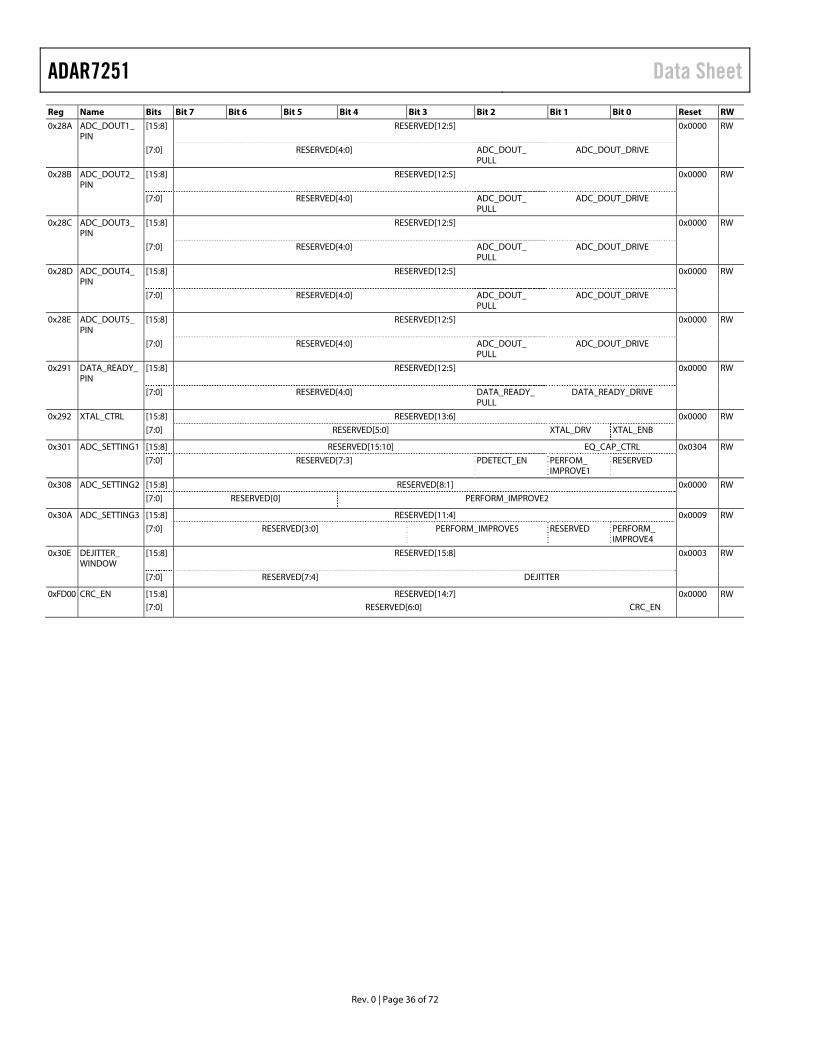
ADAR7251 Data Sheet
Rev. 0 | Page 36 of 72
Reg Name Bits Bit 7 Bit 6 Bit 5 Bit 4 Bit 3 Bit 2 Bit 1 Bit 0 Reset RW
0x28A ADC_DOUT1_ PIN
[15:8] RESERVED[12:5] 0x0000 RW
[7:0] RESERVED[4:0] ADC_DOUT_ PULL
ADC_DOUT_DRIVE
0x28B ADC_DOUT2_ PIN
[15:8] RESERVED[12:5] 0x0000 RW
[7:0] RESERVED[4:0] ADC_DOUT_ PULL
ADC_DOUT_DRIVE
0x28C ADC_DOUT3_ PIN
[15:8] RESERVED[12:5] 0x0000 RW
[7:0] RESERVED[4:0] ADC_DOUT_ PULL
ADC_DOUT_DRIVE
0x28D ADC_DOUT4_ PIN
[15:8] RESERVED[12:5] 0x0000 RW
[7:0] RESERVED[4:0] ADC_DOUT_ PULL
ADC_DOUT_DRIVE
0x28E ADC_DOUT5_ PIN
[15:8] RESERVED[12:5] 0x0000 RW
[7:0] RESERVED[4:0] ADC_DOUT_ PULL
ADC_DOUT_DRIVE
0x291 DATA_READY_PIN
[15:8] RESERVED[12:5] 0x0000 RW
[7:0] RESERVED[4:0] DATA_READY_ PULL
DATA_READY_DRIVE
0x292 XTAL_CTRL [15:8] RESERVED[13:6] 0x0000 RW
[7:0] RESERVED[5:0] XTAL_DRV XTAL_ENB 0x301 ADC_SETTING1 [15:8] RESERVED[15:10] EQ_CAP_CTRL 0x0304 RW
[7:0] RESERVED[7:3] PDETECT_EN PERFOM_ IMPROVE1
RESERVED
0x308 ADC_SETTING2 [15:8] RESERVED[8:1] 0x0000 RW
[7:0] RESERVED[0] PERFORM_IMPROVE2 0x30A ADC_SETTING3 [15:8] RESERVED[11:4] 0x0009 RW
[7:0] RESERVED[3:0] PERFORM_IMPROVE5 RESERVED PERFORM_ IMPROVE4
0x30E DEJITTER_ WINDOW
[15:8] RESERVED[15:8] 0x0003 RW
[7:0] RESERVED[7:4] DEJITTER 0xFD00 CRC_EN [15:8] RESERVED[14:7] 0x0000 RW
[7:0] RESERVED[6:0] CRC_EN
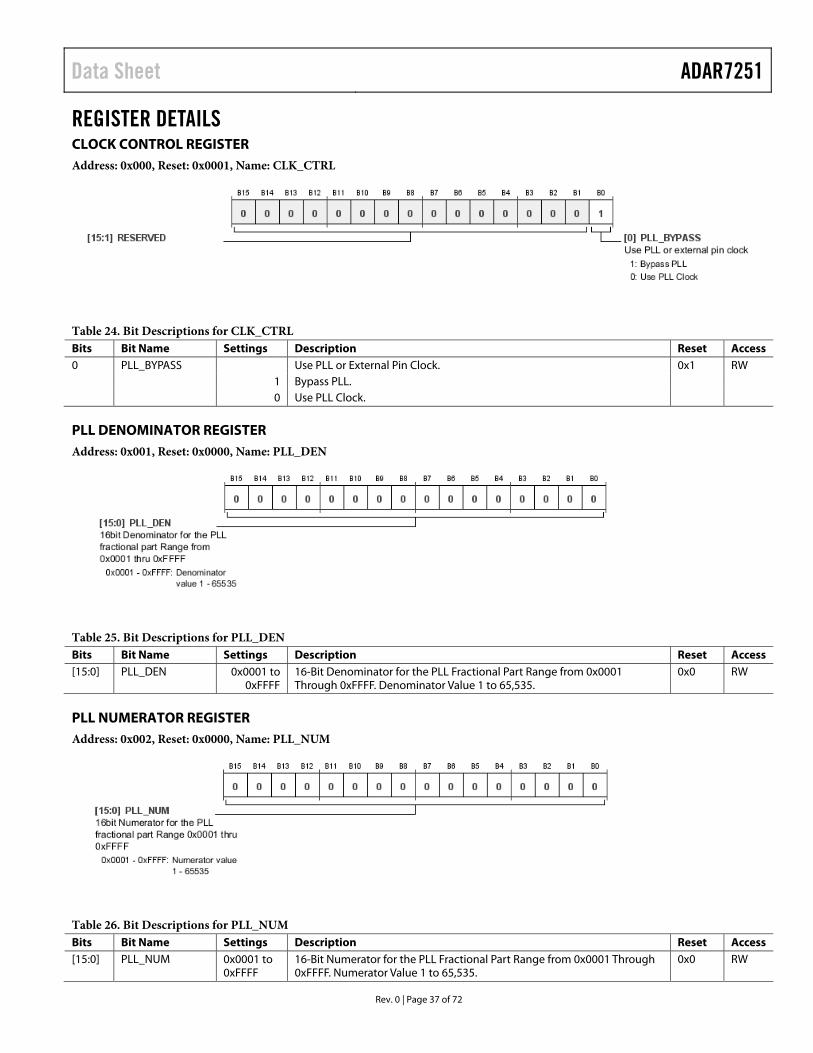
Data Sheet ADAR7251
Rev. 0 | Page 37 of 72
REGISTER DETAILS CLOCK CONTROL REGISTER Address: 0x000, Reset: 0x0001, Name: CLK_CTRL
Table 24. Bit Descriptions for CLK_CTRL Bits Bit Name Settings Description Reset Access 0 PLL_BYPASS Use PLL or External Pin Clock. 0x1 RW 1 Bypass PLL. 0 Use PLL Clock.
PLL DENOMINATOR REGISTER Address: 0x001, Reset: 0x0000, Name: PLL_DEN
Table 25. Bit Descriptions for PLL_DEN Bits Bit Name Settings Description Reset Access [15:0] PLL_DEN 0x0001 to
0xFFFF 16-Bit Denominator for the PLL Fractional Part Range from 0x0001 Through 0xFFFF. Denominator Value 1 to 65,535.
0x0 RW
PLL NUMERATOR REGISTER Address: 0x002, Reset: 0x0000, Name: PLL_NUM
Table 26. Bit Descriptions for PLL_NUM Bits Bit Name Settings Description Reset Access [15:0] PLL_NUM 0x0001 to
0xFFFF 16-Bit Numerator for the PLL Fractional Part Range from 0x0001 Through 0xFFFF. Numerator Value 1 to 65,535.
0x0 RW
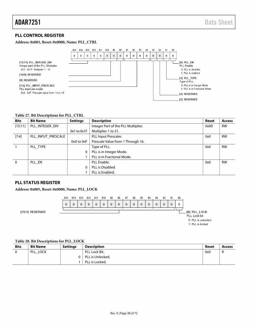
ADAR7251 Data Sheet
Rev. 0 | Page 38 of 72
PLL CONTROL REGISTER Address: 0x003, Reset: 0x0000, Name: PLL_CTRL
Table 27. Bit Descriptions for PLL_CTRL Bits Bit Name Settings Description Reset Access [15:11] PLL_INTEGER_DIV Integer Part of the PLL Multiplier. 0x00 RW 0x1 to 0x1F Multiplier 1 to 31. [7:4] PLL_INPUT_PRESCALE PLL Input Prescaler. 0x0 RW 0x0 to 0xF Prescale Value from 1 Through 16. 1 PLL_TYPE Type of PLL. 0x0 RW 0 PLL is in Integer Mode. 1 PLL is in Fractional Mode. 0 PLL_EN PLL Enable. 0x0 RW 0 PLL is Disabled. 1 PLL is Enabled.
PLL STATUS REGISTER Address: 0x005, Reset: 0x0000, Name: PLL_LOCK
Table 28. Bit Descriptions for PLL_LOCK Bits Bit Name Settings Description Reset Access 0 PLL_LOCK PLL Lock Bit. 0x0 R 0 PLL is Unlocked. 1 PLL is Locked.
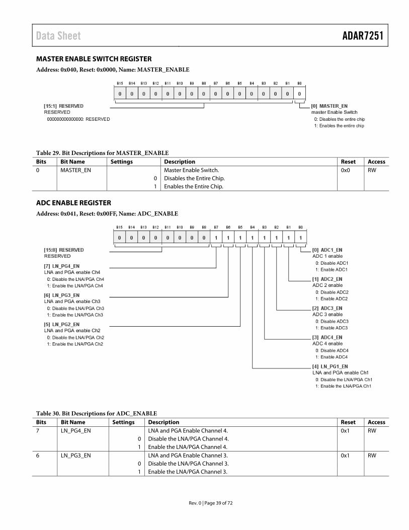
Data Sheet ADAR7251
Rev. 0 | Page 39 of 72
MASTER ENABLE SWITCH REGISTER Address: 0x040, Reset: 0x0000, Name: MASTER_ENABLE
Table 29. Bit Descriptions for MASTER_ENABLE Bits Bit Name Settings Description Reset Access 0 MASTER_EN Master Enable Switch. 0x0 RW 0 Disables the Entire Chip. 1 Enables the Entire Chip.
ADC ENABLE REGISTER Address: 0x041, Reset: 0x00FF, Name: ADC_ENABLE
Table 30. Bit Descriptions for ADC_ENABLE Bits Bit Name Settings Description Reset Access 7 LN_PG4_EN LNA and PGA Enable Channel 4. 0x1 RW 0 Disable the LNA/PGA Channel 4. 1 Enable the LNA/PGA Channel 4. 6 LN_PG3_EN LNA and PGA Enable Channel 3. 0x1 RW 0 Disable the LNA/PGA Channel 3. 1 Enable the LNA/PGA Channel 3.
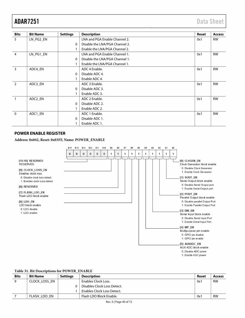
ADAR7251 Data Sheet
Rev. 0 | Page 40 of 72
Bits Bit Name Settings Description Reset Access 5 LN_PG2_EN LNA and PGA Enable Channel 2. 0x1 RW 0 Disable the LNA/PGA Channel 2. 1 Enable the LNA/PGA Channel 2. 4 LN_PG1_EN LNA and PGA Enable Channel 1. 0x1 RW 0 Disable the LNA/PGA Channel 1. 1 Enable the LNA/PGA Channel 1. 3 ADC4_EN ADC 4 Enable. 0x1 RW 0 Disable ADC 4. 1 Enable ADC 4. 2 ADC3_EN ADC 3 Enable. 0x1 RW 0 Disable ADC 3. 1 Enable ADC 3. 1 ADC2_EN ADC 2 Enable. 0x1 RW 0 Disable ADC 2. 1 Enable ADC 2. 0 ADC1_EN ADC 1 Enable. 0x1 RW 0 Disable ADC 1. 1 Enable ADC 1.
POWER ENABLE REGISTER Address: 0x042, Reset: 0x03FF, Name: POWER_ENABLE
Table 31. Bit Descriptions for POWER_ENABLE Bits Bit Name Settings Description Reset Access 9 CLOCK_LOSS_EN Enables Clock Loss. 0x1 RW 0 Disables Clock Loss Detect. 1 Enables Clock Loss Detect. 7 FLASH_LDO_EN Flash LDO Block Enable. 0x1 RW
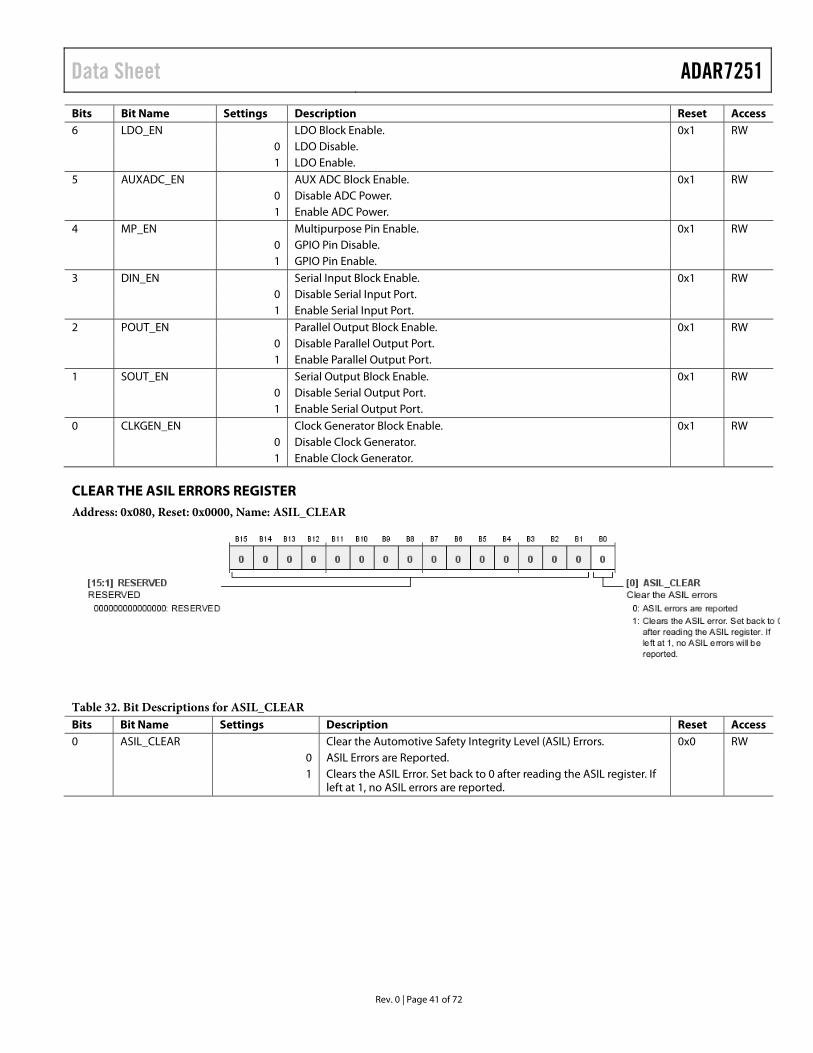
Data Sheet ADAR7251
Rev. 0 | Page 41 of 72
Bits Bit Name Settings Description Reset Access 6 LDO_EN LDO Block Enable. 0x1 RW 0 LDO Disable. 1 LDO Enable. 5 AUXADC_EN AUX ADC Block Enable. 0x1 RW 0 Disable ADC Power. 1 Enable ADC Power. 4 MP_EN Multipurpose Pin Enable. 0x1 RW 0 GPIO Pin Disable. 1 GPIO Pin Enable. 3 DIN_EN Serial Input Block Enable. 0x1 RW 0 Disable Serial Input Port. 1 Enable Serial Input Port. 2 POUT_EN Parallel Output Block Enable. 0x1 RW 0 Disable Parallel Output Port. 1 Enable Parallel Output Port. 1 SOUT_EN Serial Output Block Enable. 0x1 RW 0 Disable Serial Output Port. 1 Enable Serial Output Port. 0 CLKGEN_EN Clock Generator Block Enable. 0x1 RW 0 Disable Clock Generator. 1 Enable Clock Generator.
CLEAR THE ASIL ERRORS REGISTER Address: 0x080, Reset: 0x0000, Name: ASIL_CLEAR
Table 32. Bit Descriptions for ASIL_CLEAR Bits Bit Name Settings Description Reset Access 0 ASIL_CLEAR Clear the Automotive Safety Integrity Level (ASIL) Errors. 0x0 RW 0 ASIL Errors are Reported. 1 Clears the ASIL Error. Set back to 0 after reading the ASIL register. If
left at 1, no ASIL errors are reported.
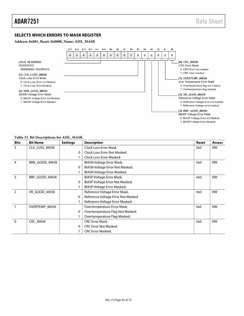
ADAR7251 Data Sheet
Rev. 0 | Page 42 of 72
SELECTS WHICH ERRORS TO MASK REGISTER Address: 0x081, Reset: 0x0000, Name: ASIL_MASK
Table 33. Bit Descriptions for ASIL_MASK Bits Bit Name Settings Description Reset Access 5 CLK_LOSS_MASK Clock Loss Error Mask. 0x0 RW 0 Clock Loss Error Not Masked. 1 Clock Loss Error Masked. 4 BRN_GOOD_MASK BIASN Voltage Error Mask. 0x0 RW 0 BIASN Voltage Error Not Masked. 1 BIASN Voltage Error Masked. 3 BRP_GOOD_MASK BIASP Voltage Error Mask. 0x0 RW 0 BIASP Voltage Error Not Masked. 1 BIASP Voltage Error Masked. 2 VR_GOOD_MASK Reference Voltage Error Mask. 0x0 RW 0 Reference Voltage Error Not Masked. 1 Reference Voltage Error Masked. 1 OVERTEMP_MASK Overtemperature Error Mask. 0x0 RW 0 Overtemperature Flag Not Masked. 1 Overtemperature Flag Masked. 0 CRC_MASK CRC Error Mask. 0x0 RW 0 CRC Error Not Masked. 1 CRC Error Masked.
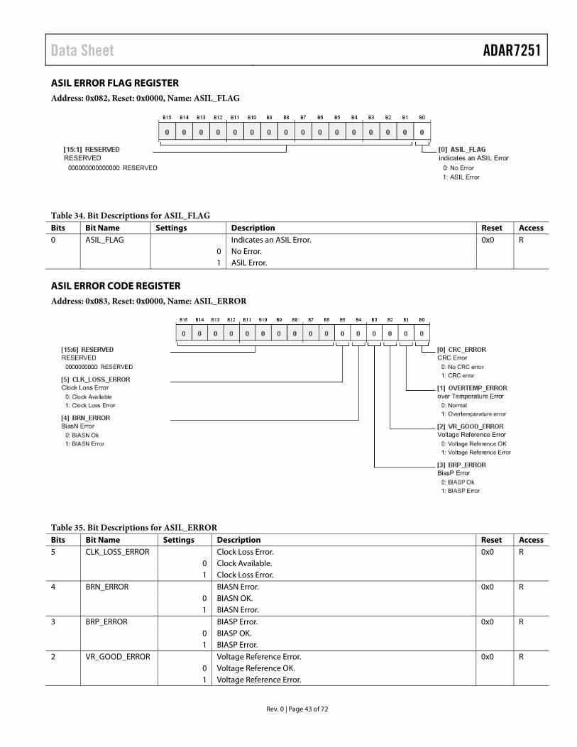
Data Sheet ADAR7251
Rev. 0 | Page 43 of 72
ASIL ERROR FLAG REGISTER Address: 0x082, Reset: 0x0000, Name: ASIL_FLAG
Table 34. Bit Descriptions for ASIL_FLAG Bits Bit Name Settings Description Reset Access 0 ASIL_FLAG Indicates an ASIL Error. 0x0 R 0 No Error. 1 ASIL Error.
ASIL ERROR CODE REGISTER Address: 0x083, Reset: 0x0000, Name: ASIL_ERROR
Table 35. Bit Descriptions for ASIL_ERROR Bits Bit Name Settings Description Reset Access 5 CLK_LOSS_ERROR Clock Loss Error. 0x0 R 0 Clock Available. 1 Clock Loss Error. 4 BRN_ERROR BIASN Error. 0x0 R 0 BIASN OK. 1 BIASN Error. 3 BRP_ERROR BIASP Error. 0x0 R 0 BIASP OK. 1 BIASP Error. 2 VR_GOOD_ERROR Voltage Reference Error. 0x0 R 0 Voltage Reference OK. 1 Voltage Reference Error.
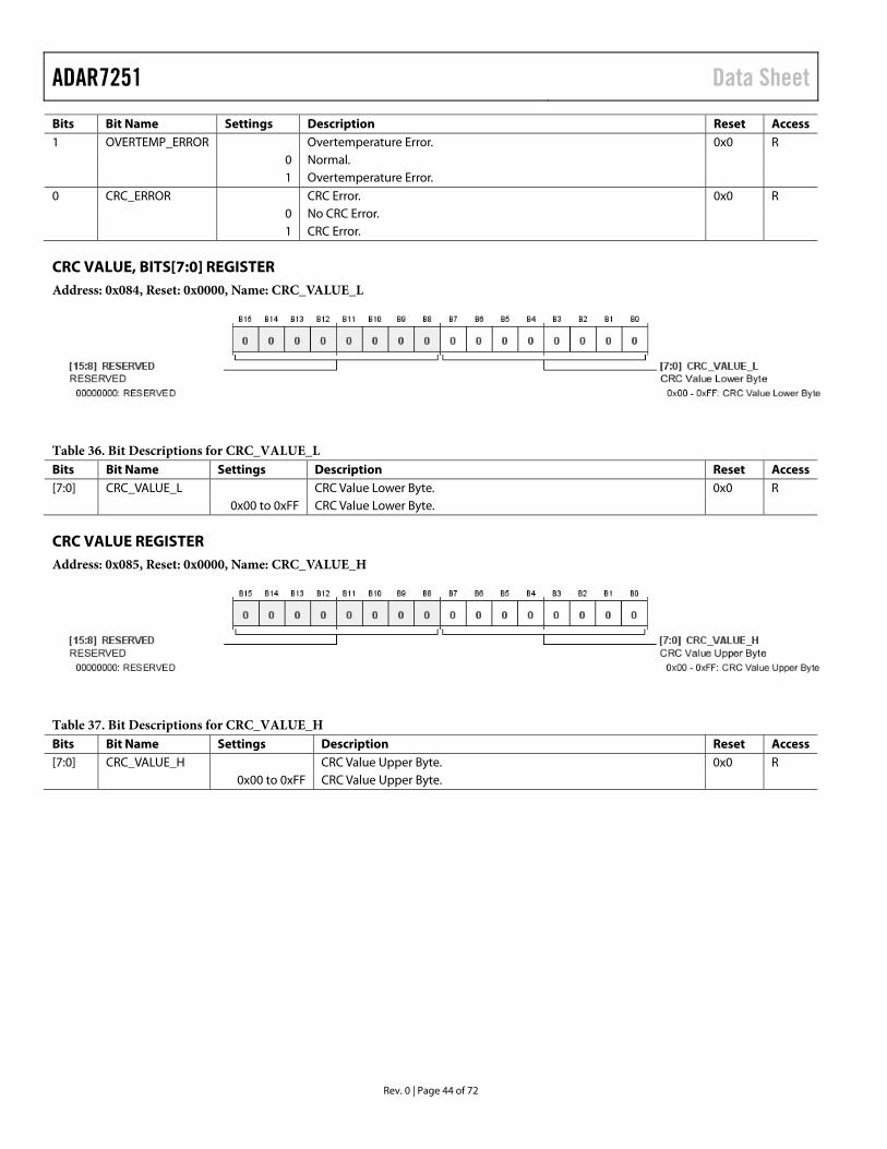
ADAR7251 Data Sheet
Rev. 0 | Page 44 of 72
Bits Bit Name Settings Description Reset Access 1 OVERTEMP_ERROR Overtemperature Error. 0x0 R 0 Normal. 1 Overtemperature Error. 0 CRC_ERROR CRC Error. 0x0 R 0 No CRC Error. 1 CRC Error.
CRC VALUE, BITS[7:0] REGISTER Address: 0x084, Reset: 0x0000, Name: CRC_VALUE_L
Table 36. Bit Descriptions for CRC_VALUE_L Bits Bit Name Settings Description Reset Access [7:0] CRC_VALUE_L CRC Value Lower Byte. 0x0 R 0x00 to 0xFF CRC Value Lower Byte.
CRC VALUE REGISTER Address: 0x085, Reset: 0x0000, Name: CRC_VALUE_H
Table 37. Bit Descriptions for CRC_VALUE_H Bits Bit Name Settings Description Reset Access [7:0] CRC_VALUE_H CRC Value Upper Byte. 0x0 R 0x00 to 0xFF CRC Value Upper Byte.
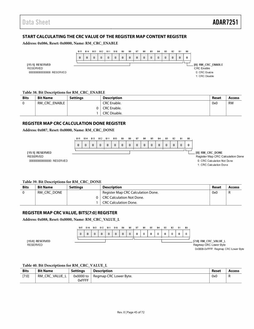
Data Sheet ADAR7251
Rev. 0 | Page 45 of 72
START CALCULATING THE CRC VALUE OF THE REGISTER MAP CONTENT REGISTER Address: 0x086, Reset: 0x0000, Name: RM_CRC_ENABLE
Table 38. Bit Descriptions for RM_CRC_ENABLE Bits Bit Name Settings Description Reset Access 0 RM_CRC_ENABLE CRC Enable. 0x0 RW 0 CRC Enable. 1 CRC Disable.
REGISTER MAP CRC CALCULATION DONE REGISTER Address: 0x087, Reset: 0x0000, Name: RM_CRC_DONE
Table 39. Bit Descriptions for RM_CRC_DONE Bits Bit Name Settings Description Reset Access 0 RM_CRC_DONE Register Map CRC Calculation Done. 0x0 R 0 CRC Calculation Not Done. 1 CRC Calculation Done.
REGISTER MAP CRC VALUE, BITS[7:0] REGISTER Address: 0x088, Reset: 0x0000, Name: RM_CRC_VALUE_L
Table 40. Bit Descriptions for RM_CRC_VALUE_L Bits Bit Name Settings Description Reset Access [7:0] RM_CRC_VALUE_L 0x0000 to
0xFFFF Regmap CRC Lower Byte. 0x0 R
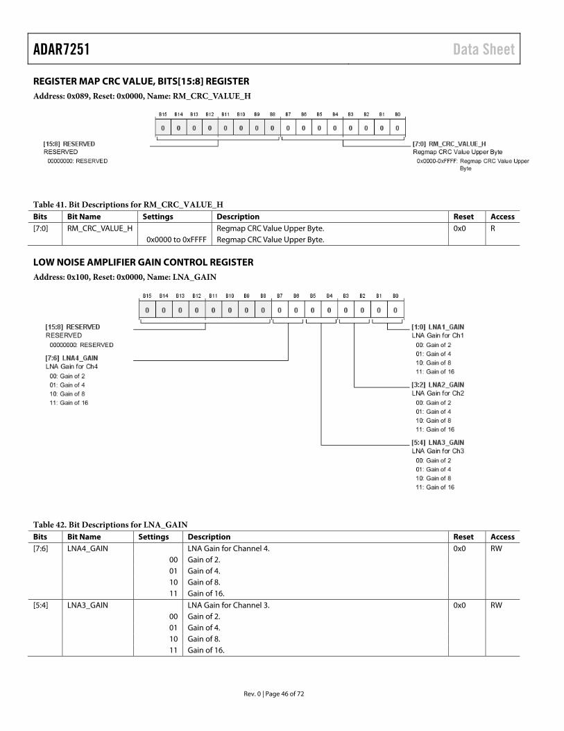
ADAR7251 Data Sheet
Rev. 0 | Page 46 of 72
REGISTER MAP CRC VALUE, BITS[15:8] REGISTER Address: 0x089, Reset: 0x0000, Name: RM_CRC_VALUE_H
Table 41. Bit Descriptions for RM_CRC_VALUE_H Bits Bit Name Settings Description Reset Access [7:0] RM_CRC_VALUE_H Regmap CRC Value Upper Byte. 0x0 R 0x0000 to 0xFFFF Regmap CRC Value Upper Byte.
LOW NOISE AMPLIFIER GAIN CONTROL REGISTER Address: 0x100, Reset: 0x0000, Name: LNA_GAIN
Table 42. Bit Descriptions for LNA_GAIN Bits Bit Name Settings Description Reset Access [7:6] LNA4_GAIN LNA Gain for Channel 4. 0x0 RW 00 Gain of 2. 01 Gain of 4. 10 Gain of 8. 11 Gain of 16. [5:4] LNA3_GAIN LNA Gain for Channel 3. 0x0 RW 00 Gain of 2. 01 Gain of 4. 10 Gain of 8. 11 Gain of 16.
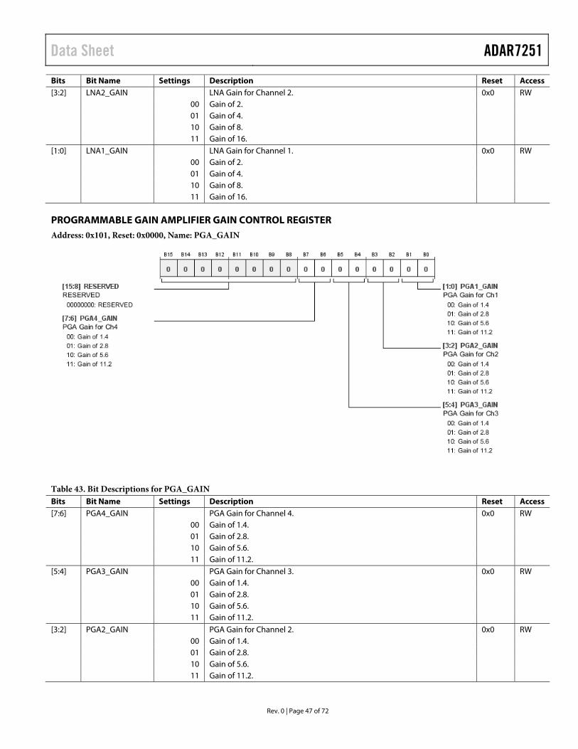
Data Sheet ADAR7251
Rev. 0 | Page 47 of 72
Bits Bit Name Settings Description Reset Access [3:2] LNA2_GAIN LNA Gain for Channel 2. 0x0 RW 00 Gain of 2. 01 Gain of 4. 10 Gain of 8. 11 Gain of 16. [1:0] LNA1_GAIN LNA Gain for Channel 1. 0x0 RW 00 Gain of 2. 01 Gain of 4. 10 Gain of 8. 11 Gain of 16.
PROGRAMMABLE GAIN AMPLIFIER GAIN CONTROL REGISTER Address: 0x101, Reset: 0x0000, Name: PGA_GAIN
Table 43. Bit Descriptions for PGA_GAIN Bits Bit Name Settings Description Reset Access [7:6] PGA4_GAIN PGA Gain for Channel 4. 0x0 RW 00 Gain of 1.4. 01 Gain of 2.8. 10 Gain of 5.6. 11 Gain of 11.2. [5:4] PGA3_GAIN PGA Gain for Channel 3. 0x0 RW 00 Gain of 1.4. 01 Gain of 2.8. 10 Gain of 5.6. 11 Gain of 11.2. [3:2] PGA2_GAIN PGA Gain for Channel 2. 0x0 RW 00 Gain of 1.4. 01 Gain of 2.8. 10 Gain of 5.6. 11 Gain of 11.2.
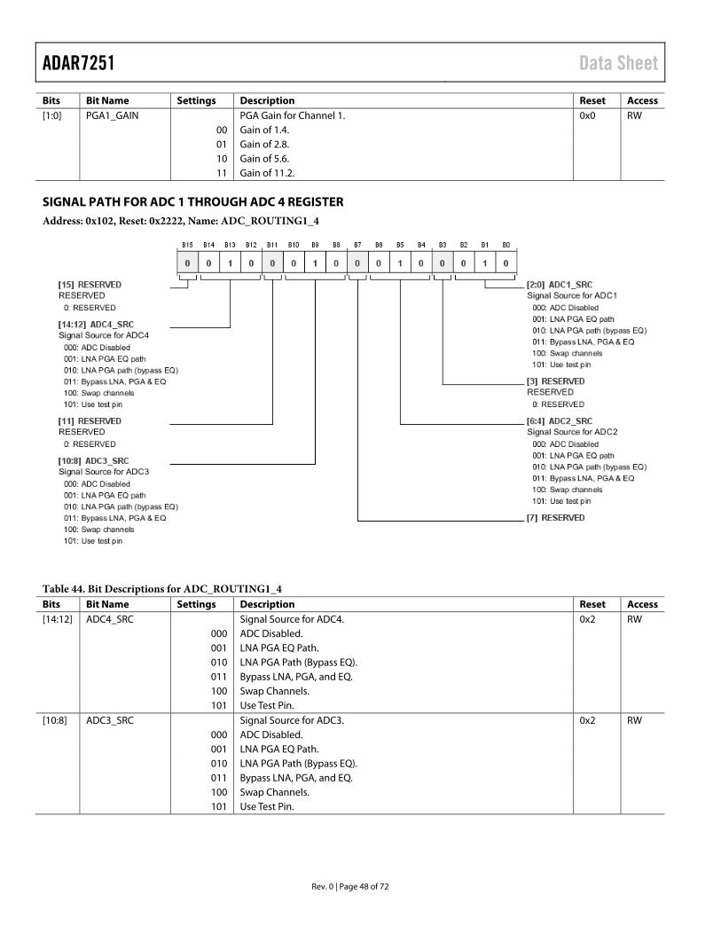
ADAR7251 Data Sheet
Rev. 0 | Page 48 of 72
Bits Bit Name Settings Description Reset Access [1:0] PGA1_GAIN PGA Gain for Channel 1. 0x0 RW 00 Gain of 1.4. 01 Gain of 2.8. 10 Gain of 5.6. 11 Gain of 11.2.
SIGNAL PATH FOR ADC 1 THROUGH ADC 4 REGISTER Address: 0x102, Reset: 0x2222, Name: ADC_ROUTING1_4
Table 44. Bit Descriptions for ADC_ROUTING1_4 Bits Bit Name Settings Description Reset Access [14:12] ADC4_SRC Signal Source for ADC4. 0x2 RW 000 ADC Disabled. 001 LNA PGA EQ Path. 010 LNA PGA Path (Bypass EQ). 011 Bypass LNA, PGA, and EQ. 100 Swap Channels. 101 Use Test Pin. [10:8] ADC3_SRC Signal Source for ADC3. 0x2 RW 000 ADC Disabled. 001 LNA PGA EQ Path. 010 LNA PGA Path (Bypass EQ). 011 Bypass LNA, PGA, and EQ. 100 Swap Channels. 101 Use Test Pin.
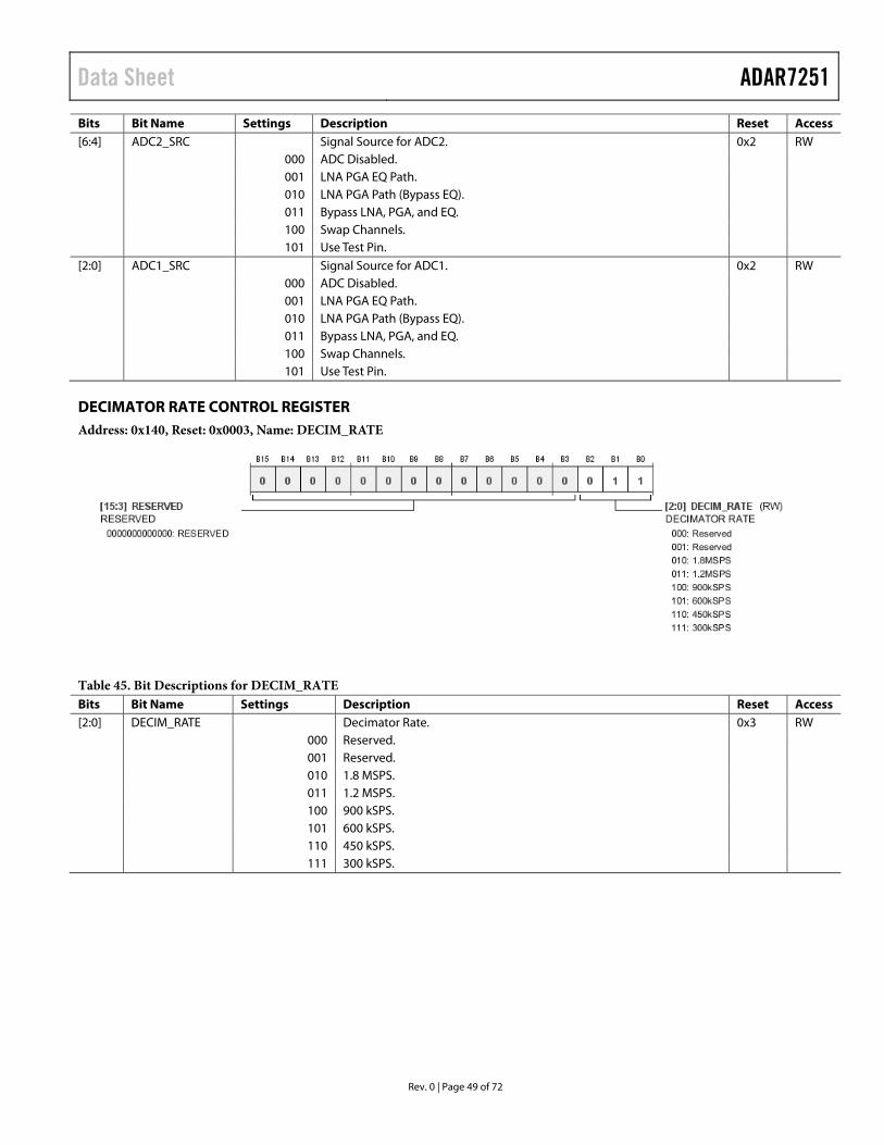
Data Sheet ADAR7251
Rev. 0 | Page 49 of 72
Bits Bit Name Settings Description Reset Access [6:4] ADC2_SRC Signal Source for ADC2. 0x2 RW 000 ADC Disabled. 001 LNA PGA EQ Path. 010 LNA PGA Path (Bypass EQ). 011 Bypass LNA, PGA, and EQ. 100 Swap Channels. 101 Use Test Pin. [2:0] ADC1_SRC Signal Source for ADC1. 0x2 RW 000 ADC Disabled. 001 LNA PGA EQ Path. 010 LNA PGA Path (Bypass EQ). 011 Bypass LNA, PGA, and EQ. 100 Swap Channels. 101 Use Test Pin.
DECIMATOR RATE CONTROL REGISTER Address: 0x140, Reset: 0x0003, Name: DECIM_RATE
Table 45. Bit Descriptions for DECIM_RATE Bits Bit Name Settings Description Reset Access [2:0] DECIM_RATE Decimator Rate. 0x3 RW 000 Reserved. 001 Reserved. 010 1.8 MSPS. 011 1.2 MSPS. 100 900 kSPS. 101 600 kSPS. 110 450 kSPS. 111 300 kSPS.
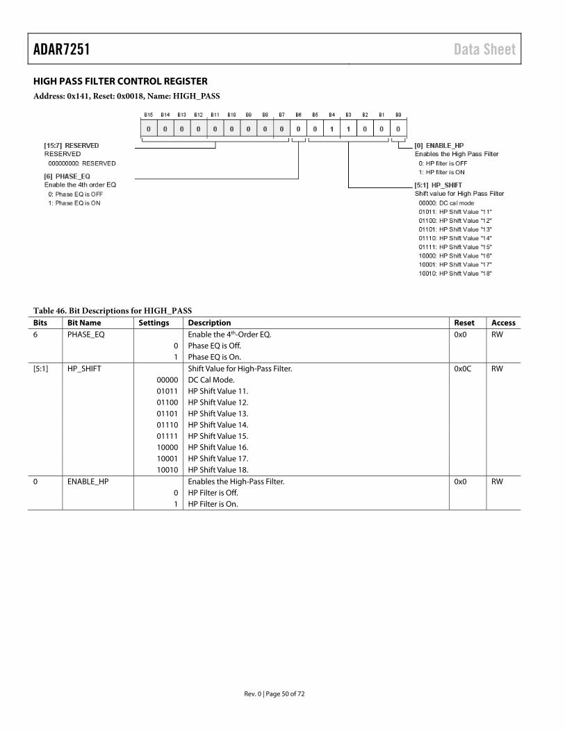
ADAR7251 Data Sheet
Rev. 0 | Page 50 of 72
HIGH PASS FILTER CONTROL REGISTER Address: 0x141, Reset: 0x0018, Name: HIGH_PASS
Table 46. Bit Descriptions for HIGH_PASS Bits Bit Name Settings Description Reset Access 6 PHASE_EQ Enable the 4th-Order EQ. 0x0 RW 0 Phase EQ is Off. 1 Phase EQ is On. [5:1] HP_SHIFT Shift Value for High-Pass Filter. 0x0C RW 00000 DC Cal Mode. 01011 HP Shift Value 11. 01100 HP Shift Value 12. 01101 HP Shift Value 13. 01110 HP Shift Value 14. 01111 HP Shift Value 15. 10000 HP Shift Value 16. 10001 HP Shift Value 17. 10010 HP Shift Value 18. 0 ENABLE_HP Enables the High-Pass Filter. 0x0 RW 0 HP Filter is Off. 1 HP Filter is On.
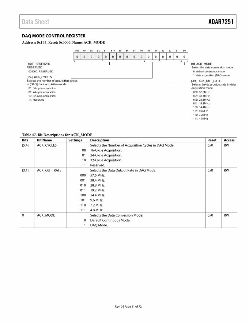
Data Sheet ADAR7251
Rev. 0 | Page 51 of 72
DAQ MODE CONTROL REGISTER Address: 0x143, Reset: 0x0000, Name: ACK_MODE
Table 47. Bit Descriptions for ACK_MODE Bits Bit Name Settings Description Reset Access [5:4] ACK_CYCLES Selects the Number of Acquisition Cycles in DAQ Mode. 0x0 RW 00 16-Cycle Acquisition. 01 24-Cycle Acquisition. 10 32-Cycle Acquisition. 11 Reserved. [3:1] ACK_OUT_RATE Selects the Data Output Rate in DAQ Mode. 0x0 RW 000 57.6 MHz. 001 38.4 MHz. 010 28.8 MHz. 011 19.2 MHz. 100 14.4 MHz. 101 9.6 MHz. 110 7.2 MHz. 111 4.8 MHz. 0 ACK_MODE Selects the Data Conversion Mode. 0x0 RW 0 Default Continuous Mode. 1 DAQ Mode.
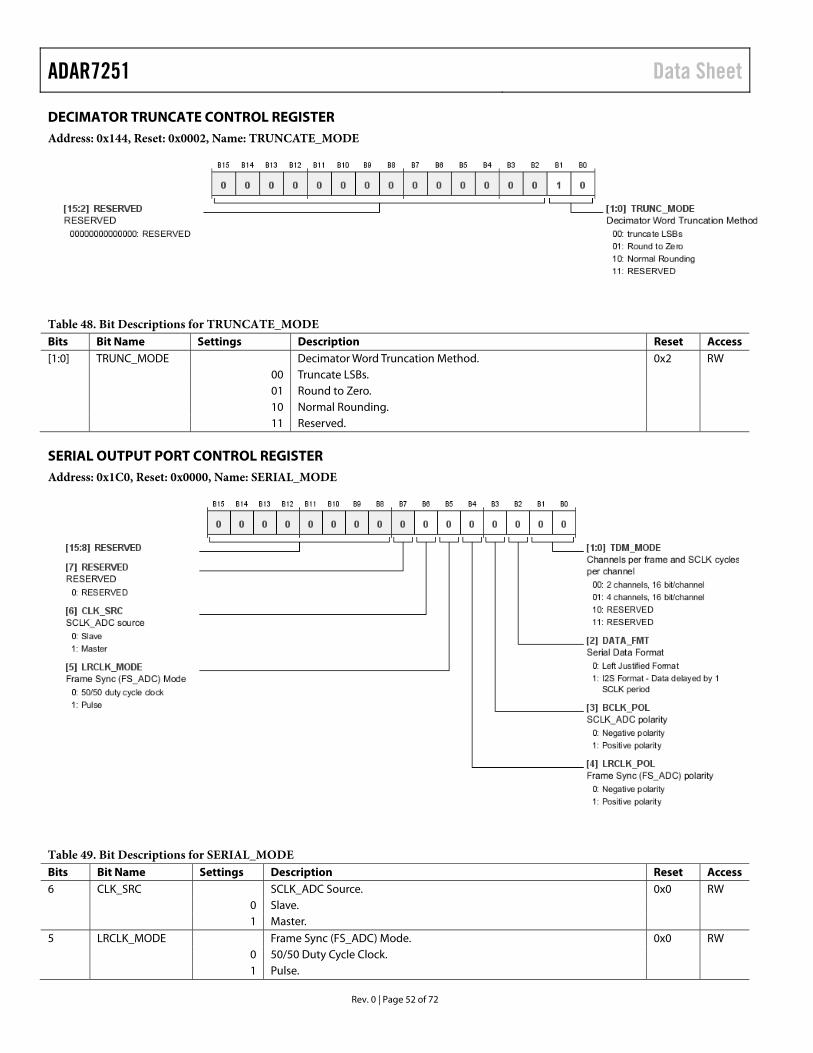
ADAR7251 Data Sheet
Rev. 0 | Page 52 of 72
DECIMATOR TRUNCATE CONTROL REGISTER Address: 0x144, Reset: 0x0002, Name: TRUNCATE_MODE
Table 48. Bit Descriptions for TRUNCATE_MODE Bits Bit Name Settings Description Reset Access [1:0] TRUNC_MODE Decimator Word Truncation Method. 0x2 RW 00 Truncate LSBs. 01 Round to Zero. 10 Normal Rounding. 11 Reserved.
SERIAL OUTPUT PORT CONTROL REGISTER Address: 0x1C0, Reset: 0x0000, Name: SERIAL_MODE
Table 49. Bit Descriptions for SERIAL_MODE Bits Bit Name Settings Description Reset Access 6 CLK_SRC SCLK_ADC Source. 0x0 RW 0 Slave. 1 Master. 5 LRCLK_MODE Frame Sync (FS_ADC) Mode. 0x0 RW 0 50/50 Duty Cycle Clock. 1 Pulse.
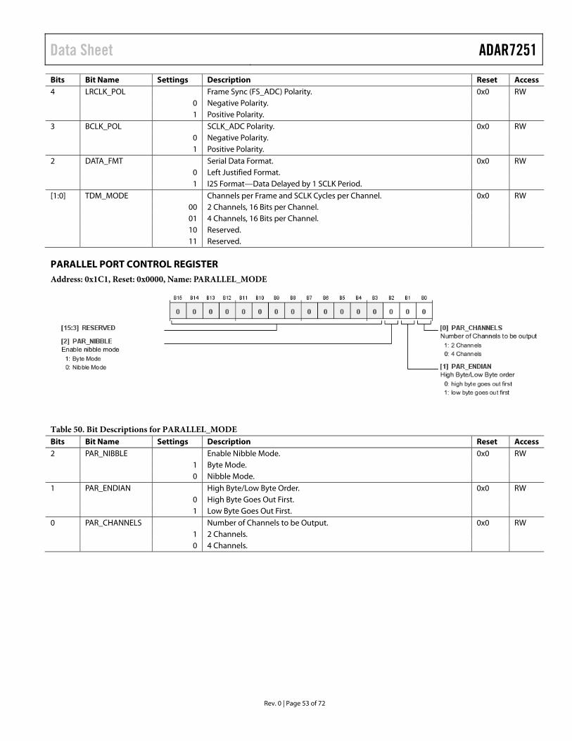
Data Sheet ADAR7251
Rev. 0 | Page 53 of 72
Bits Bit Name Settings Description Reset Access 4 LRCLK_POL Frame Sync (FS_ADC) Polarity. 0x0 RW 0 Negative Polarity. 1 Positive Polarity. 3 BCLK_POL SCLK_ADC Polarity. 0x0 RW 0 Negative Polarity. 1 Positive Polarity. 2 DATA_FMT Serial Data Format. 0x0 RW 0 Left Justified Format. 1 I2S Format—Data Delayed by 1 SCLK Period. [1:0] TDM_MODE Channels per Frame and SCLK Cycles per Channel. 0x0 RW 00 2 Channels, 16 Bits per Channel. 01 4 Channels, 16 Bits per Channel. 10 Reserved. 11 Reserved.
PARALLEL PORT CONTROL REGISTER Address: 0x1C1, Reset: 0x0000, Name: PARALLEL_MODE
Table 50. Bit Descriptions for PARALLEL_MODE Bits Bit Name Settings Description Reset Access 2 PAR_NIBBLE Enable Nibble Mode. 0x0 RW 1 Byte Mode. 0 Nibble Mode. 1 PAR_ENDIAN High Byte/Low Byte Order. 0x0 RW 0 High Byte Goes Out First. 1 Low Byte Goes Out First. 0 PAR_CHANNELS Number of Channels to be Output. 0x0 RW 1 2 Channels. 0 4 Channels.
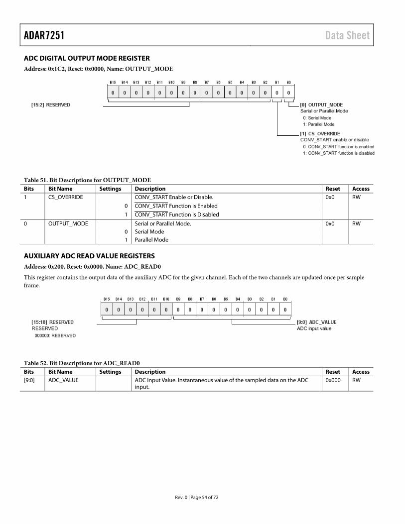
ADAR7251 Data Sheet
Rev. 0 | Page 54 of 72
ADC DIGITAL OUTPUT MODE REGISTER Address: 0x1C2, Reset: 0x0000, Name: OUTPUT_MODE
Table 51. Bit Descriptions for OUTPUT_MODE Bits Bit Name Settings Description Reset Access 1 CS_OVERRIDE CONV_START Enable or Disable. 0x0 RW
0 CONV_START Function is Enabled
1 CONV_START Function is Disabled
0 OUTPUT_MODE Serial or Parallel Mode. 0x0 RW 0 Serial Mode 1 Parallel Mode
AUXILIARY ADC READ VALUE REGISTERS Address: 0x200, Reset: 0x0000, Name: ADC_READ0
This register contains the output data of the auxiliary ADC for the given channel. Each of the two channels are updated once per sample frame.
Table 52. Bit Descriptions for ADC_READ0 Bits Bit Name Settings Description Reset Access [9:0] ADC_VALUE ADC Input Value. Instantaneous value of the sampled data on the ADC
input. 0x000 RW
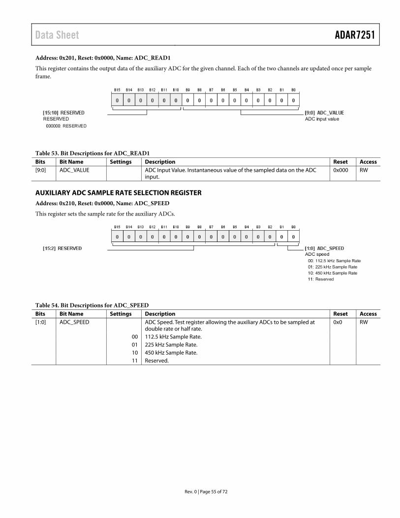
Data Sheet ADAR7251
Rev. 0 | Page 55 of 72
Address: 0x201, Reset: 0x0000, Name: ADC_READ1
This register contains the output data of the auxiliary ADC for the given channel. Each of the two channels are updated once per sample frame.
Table 53. Bit Descriptions for ADC_READ1 Bits Bit Name Settings Description Reset Access [9:0] ADC_VALUE ADC Input Value. Instantaneous value of the sampled data on the ADC
input. 0x000 RW
AUXILIARY ADC SAMPLE RATE SELECTION REGISTER Address: 0x210, Reset: 0x0000, Name: ADC_SPEED
This register sets the sample rate for the auxiliary ADCs.
Table 54. Bit Descriptions for ADC_SPEED Bits Bit Name Settings Description Reset Access [1:0] ADC_SPEED ADC Speed. Test register allowing the auxiliary ADCs to be sampled at
double rate or half rate. 0x0 RW
00 112.5 kHz Sample Rate. 01 225 kHz Sample Rate. 10 450 kHz Sample Rate. 11 Reserved.
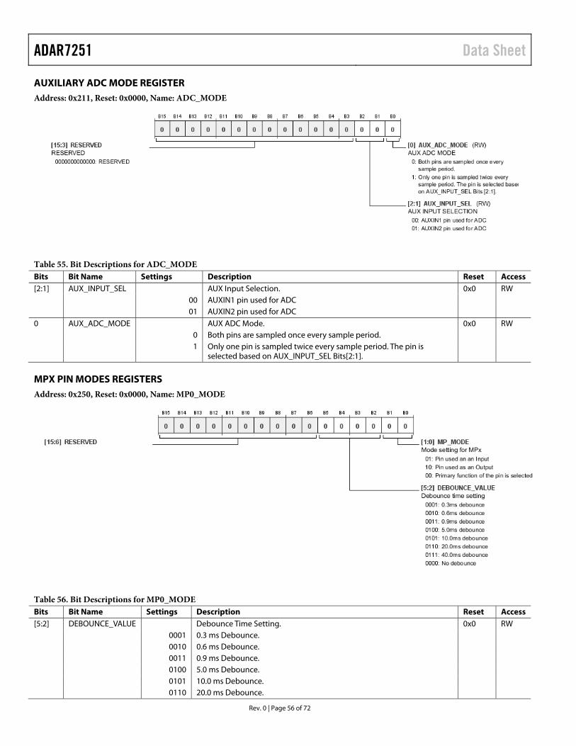
ADAR7251 Data Sheet
Rev. 0 | Page 56 of 72
AUXILIARY ADC MODE REGISTER Address: 0x211, Reset: 0x0000, Name: ADC_MODE
Table 55. Bit Descriptions for ADC_MODE Bits Bit Name Settings Description Reset Access [2:1] AUX_INPUT_SEL AUX Input Selection. 0x0 RW 00 AUXIN1 pin used for ADC 01 AUXIN2 pin used for ADC 0 AUX_ADC_MODE AUX ADC Mode. 0x0 RW 0 Both pins are sampled once every sample period. 1 Only one pin is sampled twice every sample period. The pin is
selected based on AUX_INPUT_SEL Bits[2:1].
MPX PIN MODES REGISTERS Address: 0x250, Reset: 0x0000, Name: MP0_MODE
Table 56. Bit Descriptions for MP0_MODE Bits Bit Name Settings Description Reset Access [5:2] DEBOUNCE_VALUE Debounce Time Setting. 0x0 RW 0001 0.3 ms Debounce. 0010 0.6 ms Debounce. 0011 0.9 ms Debounce. 0100 5.0 ms Debounce. 0101 10.0 ms Debounce. 0110 20.0 ms Debounce.
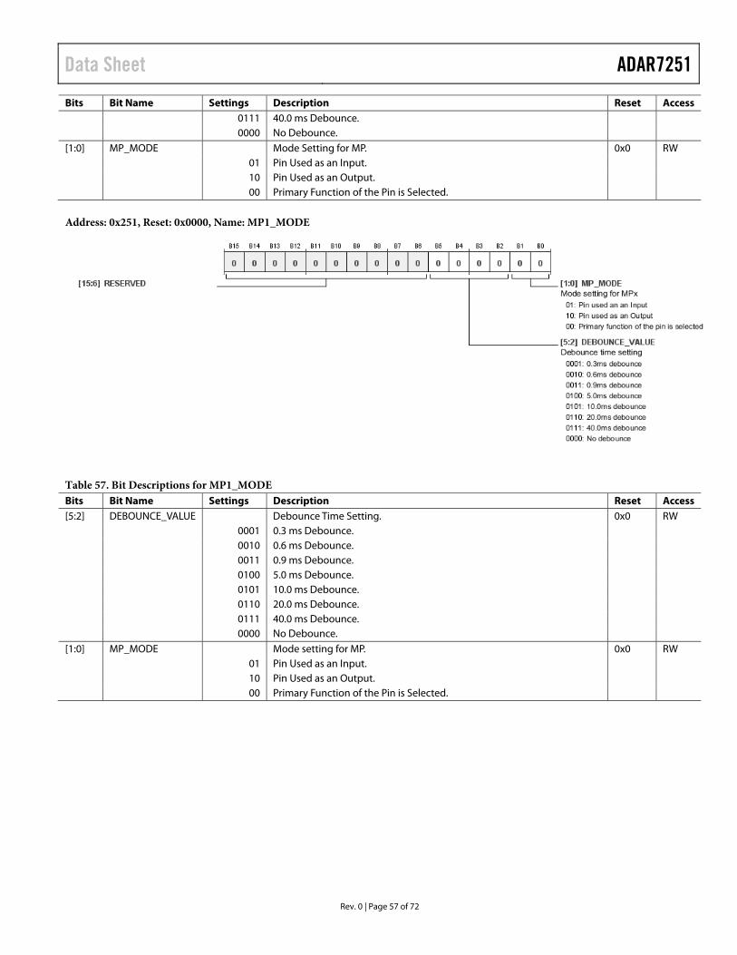
Data Sheet ADAR7251
Rev. 0 | Page 57 of 72
Bits Bit Name Settings Description Reset Access 0111 40.0 ms Debounce. 0000 No Debounce. [1:0] MP_MODE Mode Setting for MP. 0x0 RW 01 Pin Used as an Input. 10 Pin Used as an Output. 00 Primary Function of the Pin is Selected.
Address: 0x251, Reset: 0x0000, Name: MP1_MODE
Table 57. Bit Descriptions for MP1_MODE Bits Bit Name Settings Description Reset Access [5:2] DEBOUNCE_VALUE Debounce Time Setting. 0x0 RW 0001 0.3 ms Debounce. 0010 0.6 ms Debounce. 0011 0.9 ms Debounce. 0100 5.0 ms Debounce. 0101 10.0 ms Debounce. 0110 20.0 ms Debounce. 0111 40.0 ms Debounce. 0000 No Debounce. [1:0] MP_MODE Mode setting for MP. 0x0 RW 01 Pin Used as an Input. 10 Pin Used as an Output. 00 Primary Function of the Pin is Selected.
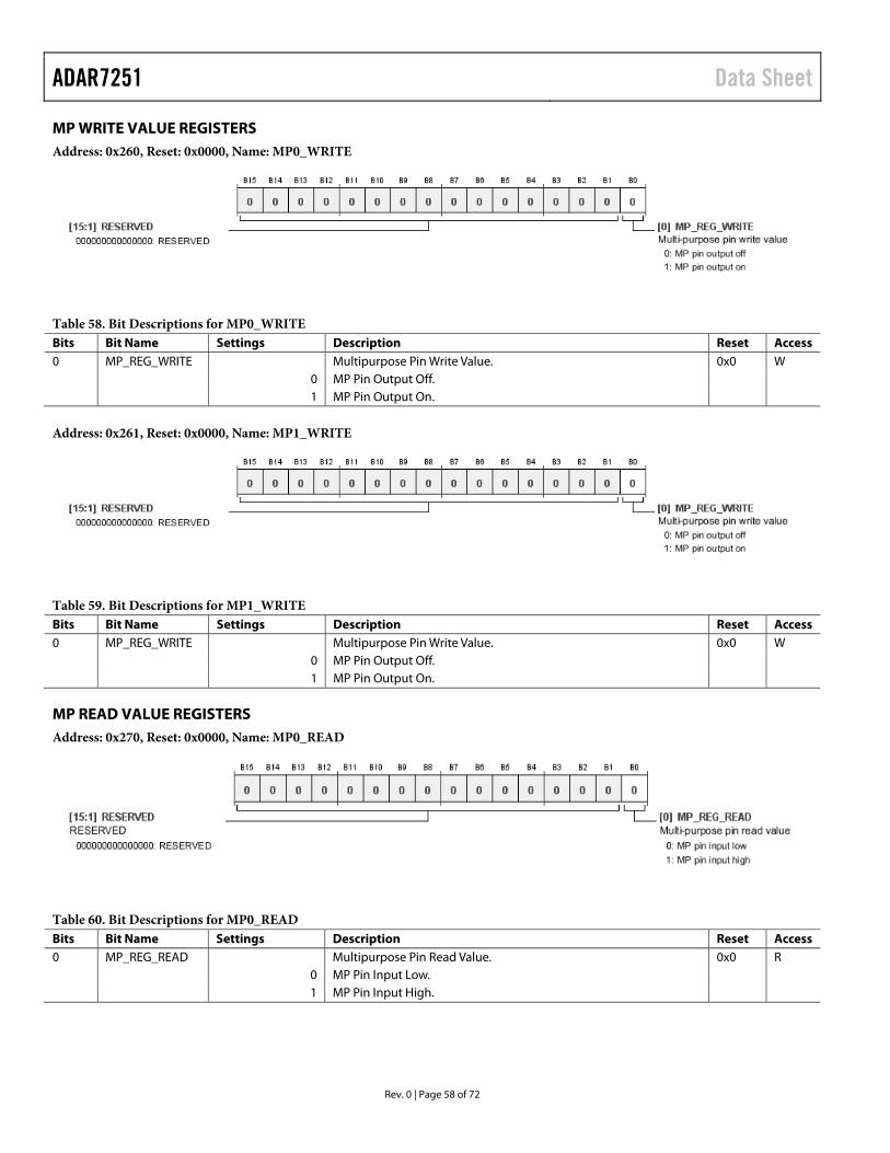
ADAR7251 Data Sheet
Rev. 0 | Page 58 of 72
MP WRITE VALUE REGISTERS Address: 0x260, Reset: 0x0000, Name: MP0_WRITE
Table 58. Bit Descriptions for MP0_WRITE Bits Bit Name Settings Description Reset Access 0 MP_REG_WRITE Multipurpose Pin Write Value. 0x0 W 0 MP Pin Output Off. 1 MP Pin Output On.
Address: 0x261, Reset: 0x0000, Name: MP1_WRITE
Table 59. Bit Descriptions for MP1_WRITE Bits Bit Name Settings Description Reset Access 0 MP_REG_WRITE Multipurpose Pin Write Value. 0x0 W 0 MP Pin Output Off. 1 MP Pin Output On.
MP READ VALUE REGISTERS Address: 0x270, Reset: 0x0000, Name: MP0_READ
Table 60. Bit Descriptions for MP0_READ Bits Bit Name Settings Description Reset Access 0 MP_REG_READ Multipurpose Pin Read Value. 0x0 R 0 MP Pin Input Low. 1 MP Pin Input High.
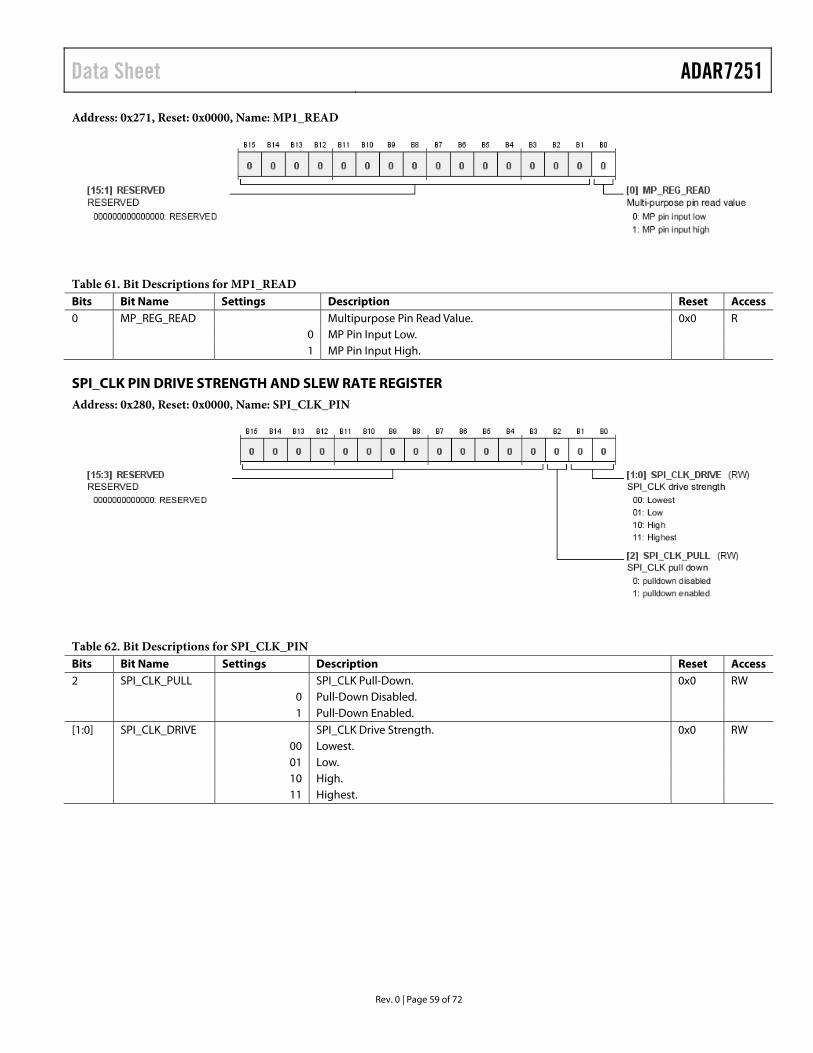
Data Sheet ADAR7251
Rev. 0 | Page 59 of 72
Address: 0x271, Reset: 0x0000, Name: MP1_READ
Table 61. Bit Descriptions for MP1_READ Bits Bit Name Settings Description Reset Access 0 MP_REG_READ Multipurpose Pin Read Value. 0x0 R 0 MP Pin Input Low. 1 MP Pin Input High.
SPI_CLK PIN DRIVE STRENGTH AND SLEW RATE REGISTER Address: 0x280, Reset: 0x0000, Name: SPI_CLK_PIN
Table 62. Bit Descriptions for SPI_CLK_PIN Bits Bit Name Settings Description Reset Access 2 SPI_CLK_PULL SPI_CLK Pull-Down. 0x0 RW 0 Pull-Down Disabled. 1 Pull-Down Enabled. [1:0] SPI_CLK_DRIVE SPI_CLK Drive Strength. 0x0 RW 00 Lowest. 01 Low. 10 High. 11 Highest.
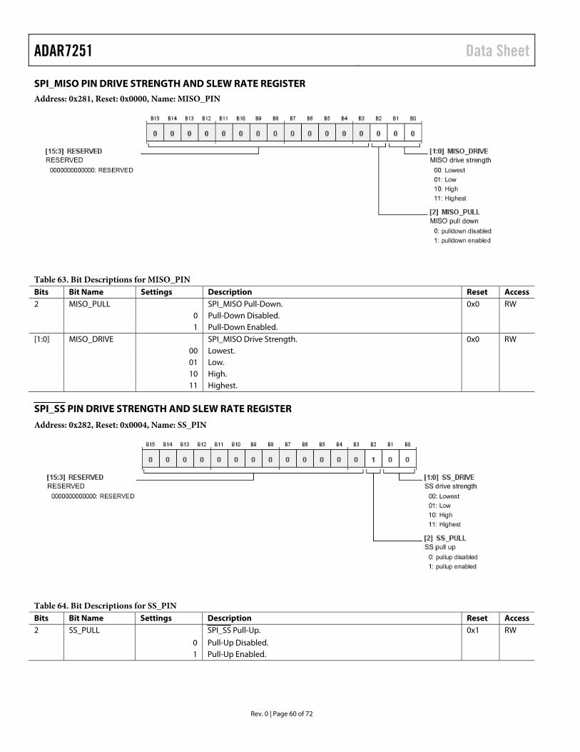
ADAR7251 Data Sheet
Rev. 0 | Page 60 of 72
SPI_MISO PIN DRIVE STRENGTH AND SLEW RATE REGISTER Address: 0x281, Reset: 0x0000, Name: MISO_PIN
Table 63. Bit Descriptions for MISO_PIN Bits Bit Name Settings Description Reset Access 2 MISO_PULL SPI_MISO Pull-Down. 0x0 RW 0 Pull-Down Disabled. 1 Pull-Down Enabled. [1:0] MISO_DRIVE SPI_MISO Drive Strength. 0x0 RW 00 Lowest. 01 Low. 10 High. 11 Highest.
SPI_SS PIN DRIVE STRENGTH AND SLEW RATE REGISTER
Address: 0x282, Reset: 0x0004, Name: SS_PIN
Table 64. Bit Descriptions for SS_PIN Bits Bit Name Settings Description Reset Access 2 SS_PULL SPI_SS Pull-Up. 0x1 RW
0 Pull-Up Disabled. 1 Pull-Up Enabled.
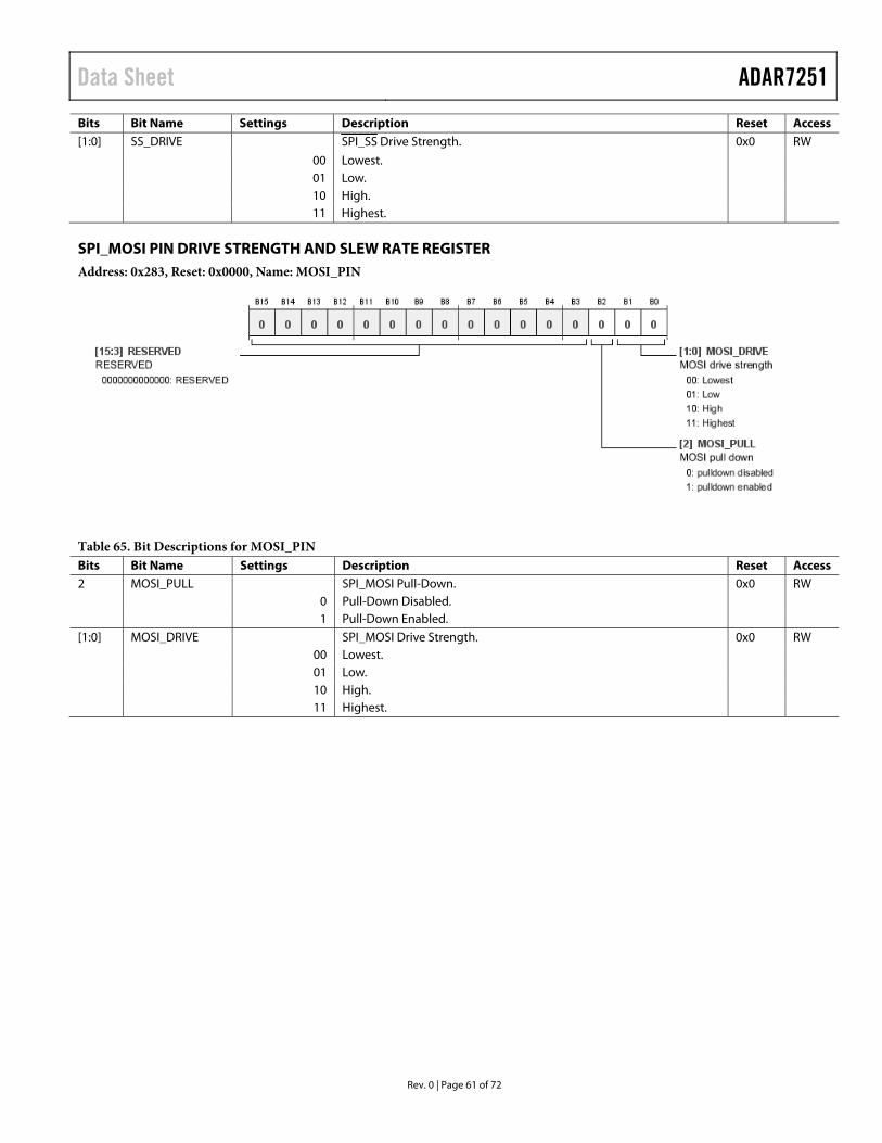
Data Sheet ADAR7251
Rev. 0 | Page 61 of 72
Bits Bit Name Settings Description Reset Access [1:0] SS_DRIVE SPI_SS Drive Strength. 0x0 RW
00 Lowest. 01 Low. 10 High. 11 Highest.
SPI_MOSI PIN DRIVE STRENGTH AND SLEW RATE REGISTER Address: 0x283, Reset: 0x0000, Name: MOSI_PIN
Table 65. Bit Descriptions for MOSI_PIN Bits Bit Name Settings Description Reset Access 2 MOSI_PULL SPI_MOSI Pull-Down. 0x0 RW 0 Pull-Down Disabled. 1 Pull-Down Enabled. [1:0] MOSI_DRIVE SPI_MOSI Drive Strength. 0x0 RW 00 Lowest. 01 Low. 10 High. 11 Highest.
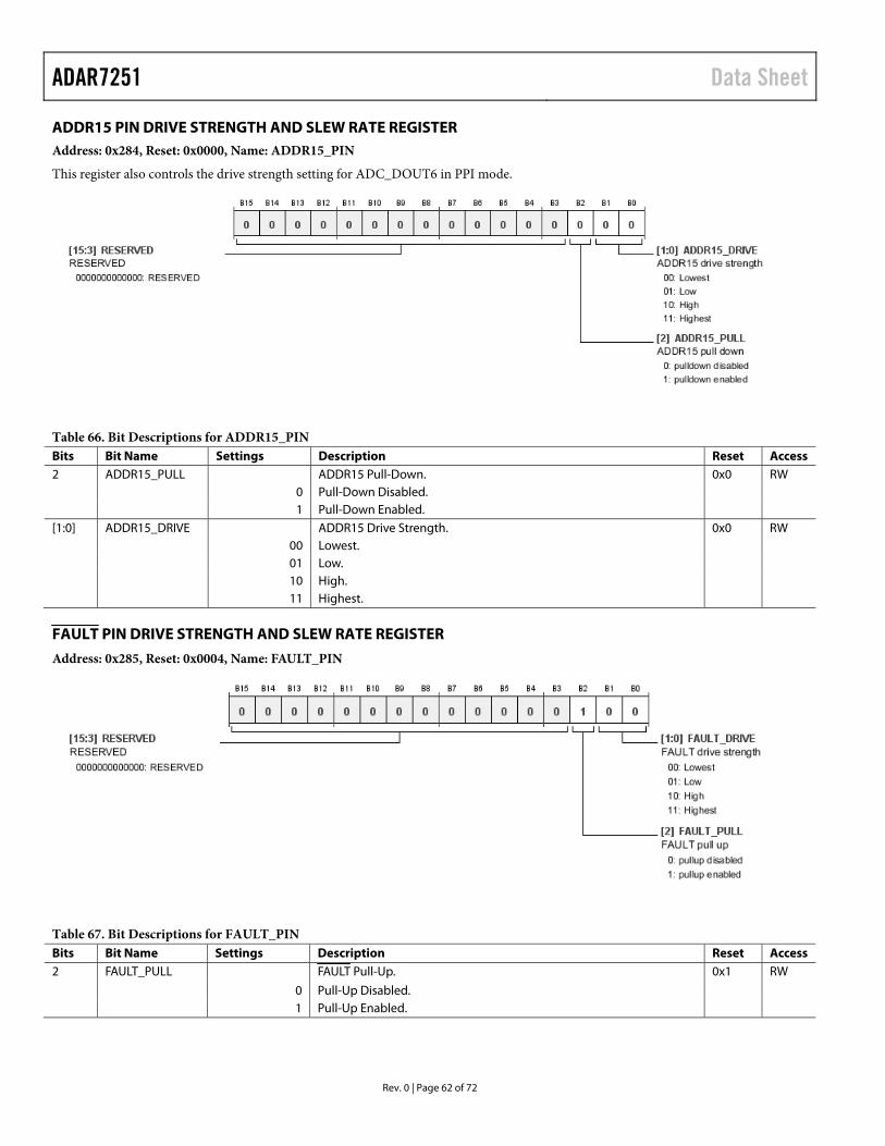
ADAR7251 Data Sheet
Rev. 0 | Page 62 of 72
ADDR15 PIN DRIVE STRENGTH AND SLEW RATE REGISTER Address: 0x284, Reset: 0x0000, Name: ADDR15_PIN
This register also controls the drive strength setting for ADC_DOUT6 in PPI mode.
Table 66. Bit Descriptions for ADDR15_PIN Bits Bit Name Settings Description Reset Access 2 ADDR15_PULL ADDR15 Pull-Down. 0x0 RW 0 Pull-Down Disabled. 1 Pull-Down Enabled. [1:0] ADDR15_DRIVE ADDR15 Drive Strength. 0x0 RW 00 Lowest. 01 Low. 10 High. 11 Highest.
FAULT PIN DRIVE STRENGTH AND SLEW RATE REGISTER
Address: 0x285, Reset: 0x0004, Name: FAULT_PIN
Table 67. Bit Descriptions for FAULT_PIN Bits Bit Name Settings Description Reset Access 2 FAULT_PULL FAULT Pull-Up. 0x1 RW
0 Pull-Up Disabled. 1 Pull-Up Enabled.
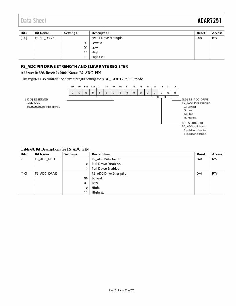
Data Sheet ADAR7251
Rev. 0 | Page 63 of 72
Bits Bit Name Settings Description Reset Access [1:0] FAULT_DRIVE FAULT Drive Strength. 0x0 RW
00 Lowest. 01 Low. 10 High. 11 Highest.
FS_ADC PIN DRIVE STRENGTH AND SLEW RATE REGISTER Address: 0x286, Reset: 0x0000, Name: FS_ADC_PIN
This register also controls the drive strength setting for ADC_DOUT7 in PPI mode.
Table 68. Bit Descriptions for FS_ADC_PIN Bits Bit Name Settings Description Reset Access 2 FS_ADC_PULL FS_ADC Pull-Down. 0x0 RW 0 Pull-Down Disabled. 1 Pull-Down Enabled. [1:0] FS_ADC_DRIVE FS_ADC Drive Strength. 0x0 RW 00 Lowest. 01 Low. 10 High. 11 Highest.
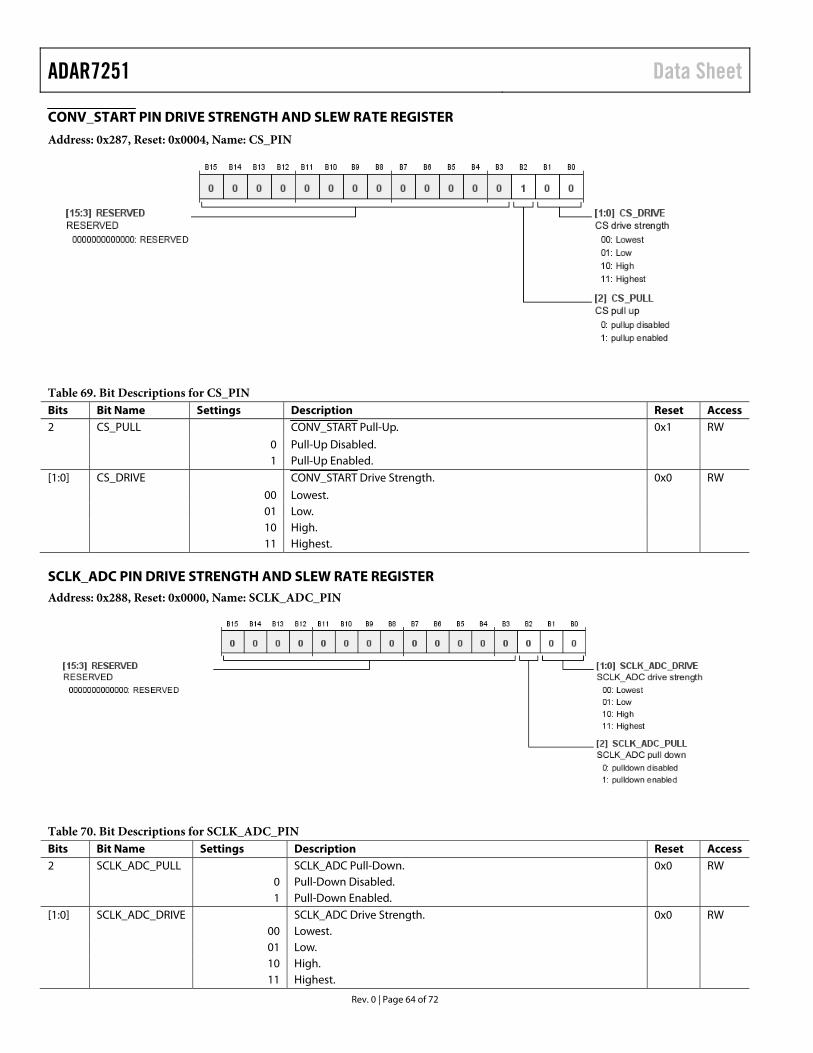
ADAR7251 Data Sheet
Rev. 0 | Page 64 of 72
CONV_START PIN DRIVE STRENGTH AND SLEW RATE REGISTER
Address: 0x287, Reset: 0x0004, Name: CS_PIN
Table 69. Bit Descriptions for CS_PIN Bits Bit Name Settings Description Reset Access 2 CS_PULL CONV_START Pull-Up. 0x1 RW
0 Pull-Up Disabled. 1 Pull-Up Enabled. [1:0] CS_DRIVE CONV_START Drive Strength. 0x0 RW
00 Lowest. 01 Low. 10 High. 11 Highest.
SCLK_ADC PIN DRIVE STRENGTH AND SLEW RATE REGISTER Address: 0x288, Reset: 0x0000, Name: SCLK_ADC_PIN
Table 70. Bit Descriptions for SCLK_ADC_PIN Bits Bit Name Settings Description Reset Access 2 SCLK_ADC_PULL SCLK_ADC Pull-Down. 0x0 RW 0 Pull-Down Disabled. 1 Pull-Down Enabled. [1:0] SCLK_ADC_DRIVE SCLK_ADC Drive Strength. 0x0 RW 00 Lowest. 01 Low. 10 High. 11 Highest.

Data Sheet ADAR7251
Rev. 0 | Page 65 of 72
ADC_DOUTX PINS DRIVE STRENGTH AND SLEW RATE REGISTERS The following registers refer to the ADC_DOUTx pins. This range includes ADC_DOUT0 through ADC_DOUT5. For Bits[1:0] and Bit 2 in Table 71 through Table 76, ADC_DOUT refers to the ADC_DOUTx pin defined by the register name.
Address: 0x289, Reset: 0x0000, Name: ADC_DOUT0_PIN
Table 71. Bit Descriptions for ADC_DOUT0_PIN Bits Bit Name Settings Description Reset Access 2 ADC_DOUT_PULL ADC_DOUT Pull-Down. 0x0 RW 0 Pull-Down Disabled. 1 Pull-Down Enabled. [1:0] ADC_DOUT_DRIVE ADC_DOUT Drive Strength. 0x0 RW 00 Lowest. 01 Low. 10 High. 11 Highest.
Address: 0x28A, Reset: 0x0000, Name: ADC_DOUT1_PIN
Table 72. Bit Descriptions for ADC_DOUT1_PIN Bits Bit Name Settings Description Reset Access 2 ADC_DOUT_PULL ADC_DOUT Pull-Down. 0x0 RW 0 Pull-Down Disabled. 1 Pull-Down Enabled. [1:0] ADC_DOUT_DRIVE ADC_DOUT Drive Strength. 0x0 RW 00 Lowest. 01 Low. 10 High. 11 Highest.
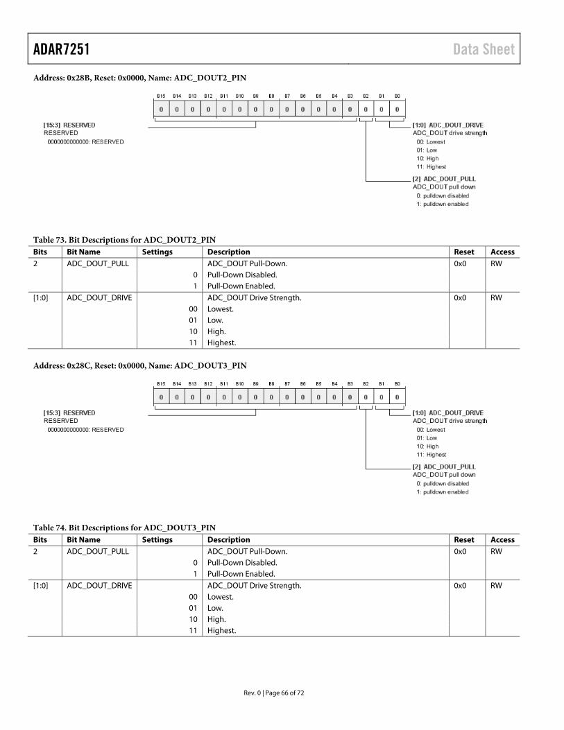
ADAR7251 Data Sheet
Rev. 0 | Page 66 of 72
Address: 0x28B, Reset: 0x0000, Name: ADC_DOUT2_PIN
Table 73. Bit Descriptions for ADC_DOUT2_PIN Bits Bit Name Settings Description Reset Access 2 ADC_DOUT_PULL ADC_DOUT Pull-Down. 0x0 RW 0 Pull-Down Disabled. 1 Pull-Down Enabled. [1:0] ADC_DOUT_DRIVE ADC_DOUT Drive Strength. 0x0 RW 00 Lowest. 01 Low. 10 High. 11 Highest.
Address: 0x28C, Reset: 0x0000, Name: ADC_DOUT3_PIN
Table 74. Bit Descriptions for ADC_DOUT3_PIN Bits Bit Name Settings Description Reset Access 2 ADC_DOUT_PULL ADC_DOUT Pull-Down. 0x0 RW 0 Pull-Down Disabled. 1 Pull-Down Enabled. [1:0] ADC_DOUT_DRIVE ADC_DOUT Drive Strength. 0x0 RW 00 Lowest. 01 Low. 10 High. 11 Highest.
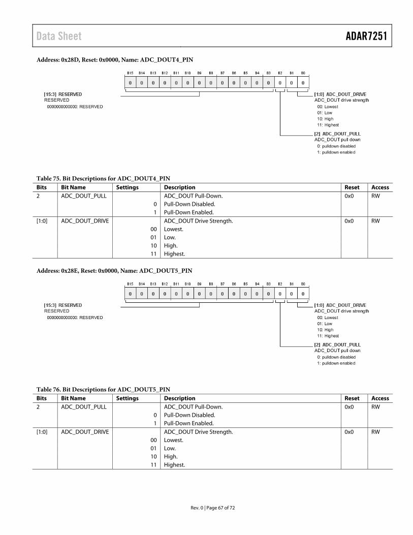
Data Sheet ADAR7251
Rev. 0 | Page 67 of 72
Address: 0x28D, Reset: 0x0000, Name: ADC_DOUT4_PIN
Table 75. Bit Descriptions for ADC_DOUT4_PIN Bits Bit Name Settings Description Reset Access 2 ADC_DOUT_PULL ADC_DOUT Pull-Down. 0x0 RW 0 Pull-Down Disabled. 1 Pull-Down Enabled. [1:0] ADC_DOUT_DRIVE ADC_DOUT Drive Strength. 0x0 RW 00 Lowest. 01 Low. 10 High. 11 Highest.
Address: 0x28E, Reset: 0x0000, Name: ADC_DOUT5_PIN
Table 76. Bit Descriptions for ADC_DOUT5_PIN Bits Bit Name Settings Description Reset Access 2 ADC_DOUT_PULL ADC_DOUT Pull-Down. 0x0 RW 0 Pull-Down Disabled. 1 Pull-Down Enabled. [1:0] ADC_DOUT_DRIVE ADC_DOUT Drive Strength. 0x0 RW 00 Lowest. 01 Low. 10 High. 11 Highest.
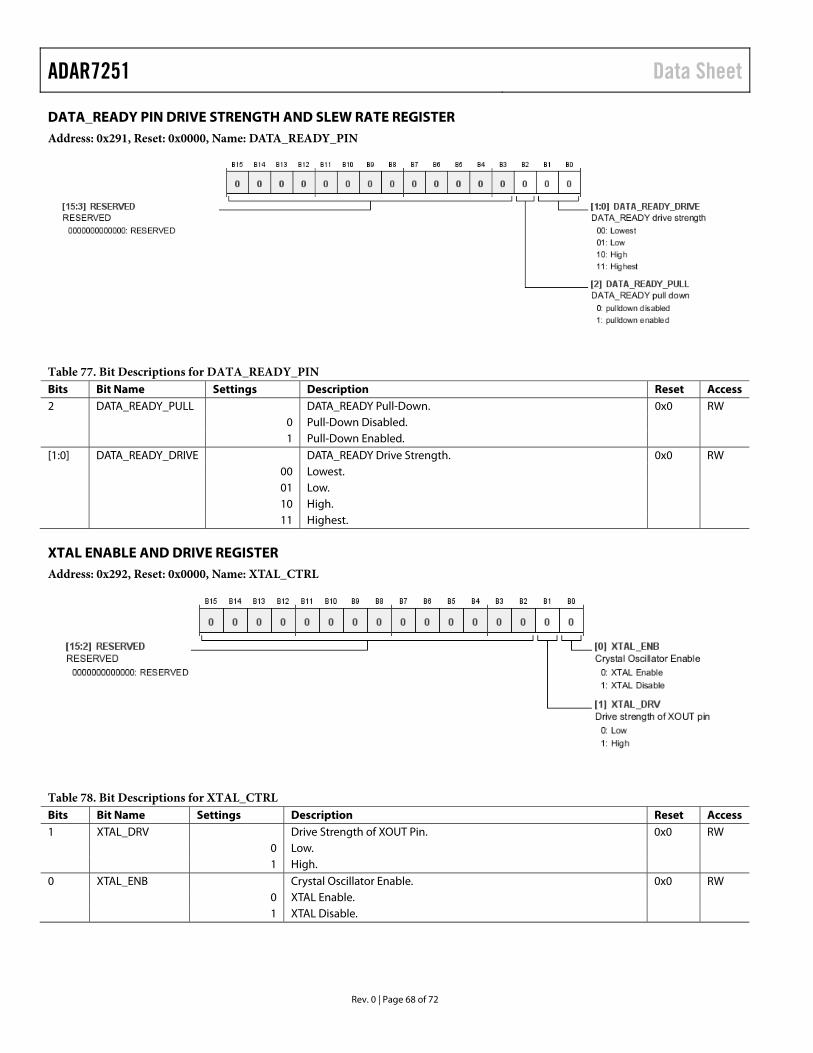
ADAR7251 Data Sheet
Rev. 0 | Page 68 of 72
DATA_READY PIN DRIVE STRENGTH AND SLEW RATE REGISTER Address: 0x291, Reset: 0x0000, Name: DATA_READY_PIN
Table 77. Bit Descriptions for DATA_READY_PIN Bits Bit Name Settings Description Reset Access 2 DATA_READY_PULL DATA_READY Pull-Down. 0x0 RW 0 Pull-Down Disabled. 1 Pull-Down Enabled. [1:0] DATA_READY_DRIVE DATA_READY Drive Strength. 0x0 RW 00 Lowest. 01 Low. 10 High. 11 Highest.
XTAL ENABLE AND DRIVE REGISTER Address: 0x292, Reset: 0x0000, Name: XTAL_CTRL
Table 78. Bit Descriptions for XTAL_CTRL Bits Bit Name Settings Description Reset Access 1 XTAL_DRV Drive Strength of XOUT Pin. 0x0 RW 0 Low. 1 High. 0 XTAL_ENB Crystal Oscillator Enable. 0x0 RW 0 XTAL Enable. 1 XTAL Disable.
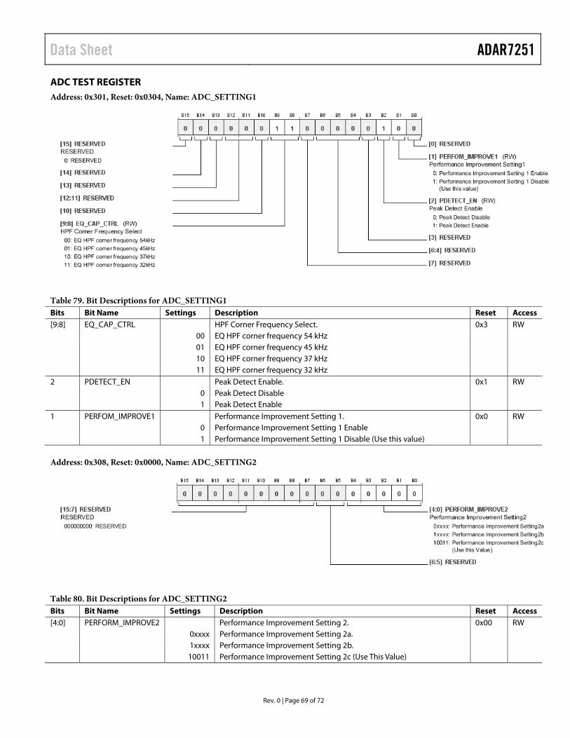
Data Sheet ADAR7251
Rev. 0 | Page 69 of 72
ADC TEST REGISTER Address: 0x301, Reset: 0x0304, Name: ADC_SETTING1
Table 79. Bit Descriptions for ADC_SETTING1 Bits Bit Name Settings Description Reset Access [9:8] EQ_CAP_CTRL HPF Corner Frequency Select. 0x3 RW 00 EQ HPF corner frequency 54 kHz 01 EQ HPF corner frequency 45 kHz 10 EQ HPF corner frequency 37 kHz 11 EQ HPF corner frequency 32 kHz 2 PDETECT_EN Peak Detect Enable. 0x1 RW 0 Peak Detect Disable 1 Peak Detect Enable 1 PERFOM_IMPROVE1 Performance Improvement Setting 1. 0x0 RW 0 Performance Improvement Setting 1 Enable 1 Performance Improvement Setting 1 Disable (Use this value)
Address: 0x308, Reset: 0x0000, Name: ADC_SETTING2
Table 80. Bit Descriptions for ADC_SETTING2 Bits Bit Name Settings Description Reset Access [4:0] PERFORM_IMPROVE2 Performance Improvement Setting 2. 0x00 RW 0xxxx Performance Improvement Setting 2a. 1xxxx Performance Improvement Setting 2b. 10011 Performance Improvement Setting 2c (Use This Value)
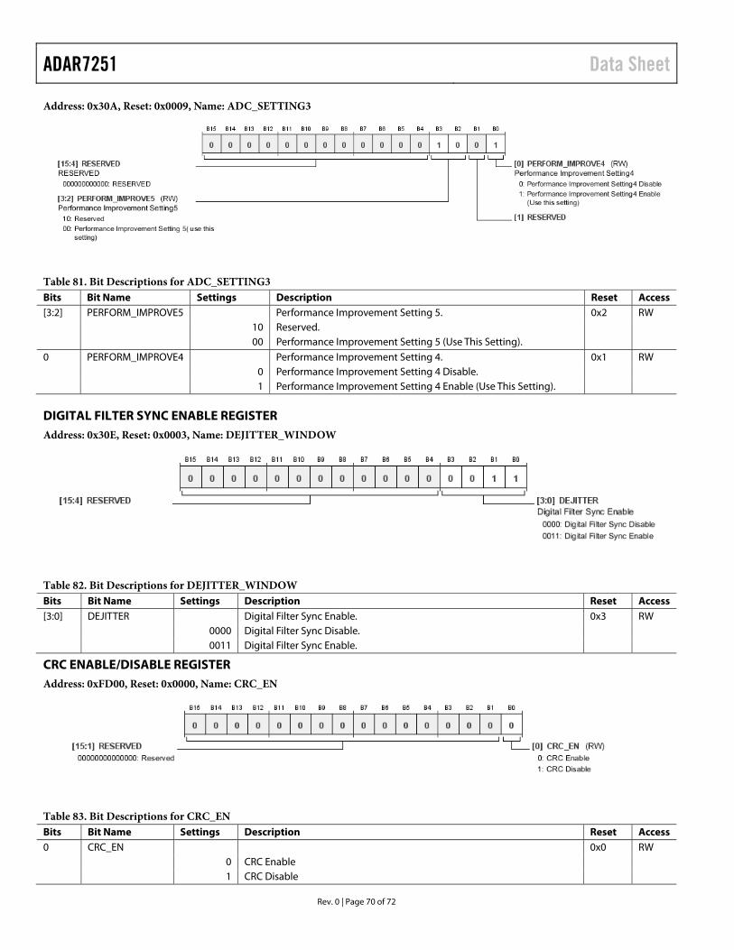
ADAR7251 Data Sheet
Rev. 0 | Page 70 of 72
Address: 0x30A, Reset: 0x0009, Name: ADC_SETTING3
Table 81. Bit Descriptions for ADC_SETTING3 Bits Bit Name Settings Description Reset Access [3:2] PERFORM_IMPROVE5 Performance Improvement Setting 5. 0x2 RW 10 Reserved. 00 Performance Improvement Setting 5 (Use This Setting). 0 PERFORM_IMPROVE4 Performance Improvement Setting 4. 0x1 RW 0 Performance Improvement Setting 4 Disable. 1 Performance Improvement Setting 4 Enable (Use This Setting).
DIGITAL FILTER SYNC ENABLE REGISTER Address: 0x30E, Reset: 0x0003, Name: DEJITTER_WINDOW
Table 82. Bit Descriptions for DEJITTER_WINDOW Bits Bit Name Settings Description Reset Access [3:0] DEJITTER Digital Filter Sync Enable. 0x3 RW 0000 Digital Filter Sync Disable. 0011 Digital Filter Sync Enable.
CRC ENABLE/DISABLE REGISTER Address: 0xFD00, Reset: 0x0000, Name: CRC_EN
Table 83. Bit Descriptions for CRC_EN Bits Bit Name Settings Description Reset Access 0 CRC_EN 0x0 RW 0 CRC Enable 1 CRC Disable
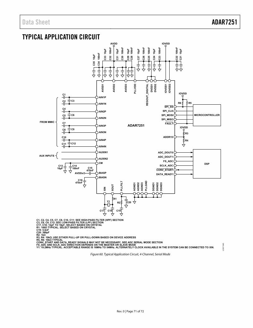
Data Sheet ADAR7251
Rev. 0 | Page 71 of 72
TYPICAL APPLICATION CIRCUIT AVDD
AIN1P
AV
DD
1
AV
DD
2
AV
DD
3
PL
LV
DD
DV
DD
1
DV
DD
2
IOV
DD
1
IOV
DD
2
RE
GO
UT
_DIG
ITA
L
C1
C2 C3AIN1N
AIN2PC4
C5 C6
FROM MMIC
AIN2N
AIN3P ADAR7251C7
C8 C9AIN3N
AIN4PC10
C11 C12
C15470nF
C16470nF
C1310µF
C14100nF
Y1R1
R4
R3
R6 R5
C18C17 C19
R2 C20
AIN4N
ADC_DOUT0
ADDR15
AUXIN1
AUXIN2
CM
BIASP
BIASN
IOVDD
C35
10
µF
C34
10
0nF
C30
10
0nF
C33
10
µF
C31
10
µF
C29
10
µF
C28
10
0nF
C27
10
µF
C24
10
µF
C26
10
0nF
C23
10
0nF
C21
10
µF
C22
10
0nF
C25
10
0nF
C32
10
0nF
AVDDx
ADC_DOUT1
FS_ADC
FAULT
SPI_MISO
SPI_MOSI
SPI_CLK
SPI_SS
SCLK_ADC
CONV_START
DATA_READY
C1, C2, C4, C5, C7, C8, C10, C11: SEE HIGH-PASS FILTER (HPF) SECTIONC3, C6, C9, C12: SEE LOW-PASS FILTER (LPF) SECTIONC17, C18: 12pF TO 18pF, SELECT BASED ON CRYSTALR1: 100Ω TYPICAL. SELECT BASED ON CRYSTALC19: 5.6nFC20: 390pFR2: 1kΩR3, R4: 10kΩ; USE EITHER PULL-UP OR PULL-DOWN BASED ON DEVICE ADDRESSR5, R6: 10kΩ TYPICALCONV_START AND DATA_READY SIGNALS MAY NOT BE NECESSARY, SEE ADC SERIAL MODE SECTIONFS_ADC AND SCLK_ADC DIRECTION DEPENDS ON THE MASTER OR SLAVE MODEY1: 19.2MHz TYPICAL. ACCEPTABLE RANGE IS 16MHz TO 54MHz. ALTERNATELY CLOCK AVAILABLE IN THE SYSTEM CAN BE CONNECTED TO XIN.
IOVDD
MICROCONTROLLER
IOVDD
XIN
XO
UT
PL
LF
ILT
AG
ND
1
AG
ND
2
AG
ND
3
PL
LG
ND
DG
ND
1
DG
ND
2
DG
ND
3
AUX INPUTS
DSP
123
57-0
45
Figure 60. Typical Application Circuit, 4-Channel, Serial Mode
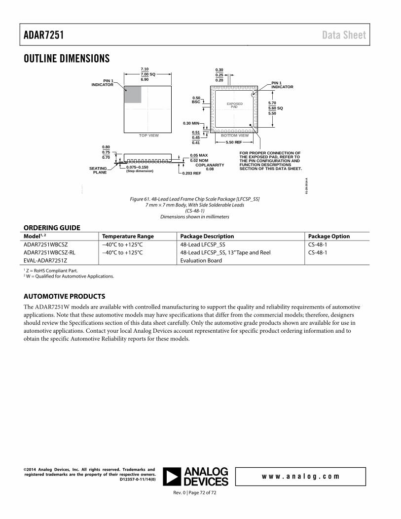
ADAR7251 Data Sheet
Rev. 0 | Page 72 of 72
OUTLINE DIMENSIONS
01-2
8-20
14-A
1
0.50BSC
BOTTOM VIEWTOP VIEW
PIN 1INDICATOR
48
1324
25
36
37
12
EXPOSEDPAD
PIN 1INDICATOR
SEATINGPLANE
0.05 MAX0.02 NOM
0.203 REF
0.30 MIN
0.075~0.150(Step dimension)
COPLANARITY0.08
0.300.250.20
7.107.00 SQ6.90
0.800.750.70
FOR PROPER CONNECTION OFTHE EXPOSED PAD, REFER TOTHE PIN CONFIGURATION ANDFUNCTION DESCRIPTIONSSECTION OF THIS DATA SHEET.
0.510.450.41
5.705.60 SQ5.50
5.50 REF
PK
G-4
27
7
Figure 61. 48-Lead Lead Frame Chip Scale Package [LFCSP_SS]
7 mm × 7 mm Body, With Side Solderable Leads (CS-48-1)
Dimensions shown in millimeters
ORDERING GUIDE Model1, 2 Temperature Range Package Description Package Option ADAR7251WBCSZ −40°C to +125°C 48-Lead LFCSP_SS CS-48-1 ADAR7251WBCSZ-RL −40°C to +125°C 48-Lead LFCSP_SS, 13” Tape and Reel CS-48-1 EVAL-ADAR7251Z Evaluation Board 1 Z = RoHS Compliant Part. 2 W = Qualified for Automotive Applications.
AUTOMOTIVE PRODUCTS The ADAR7251W models are available with controlled manufacturing to support the quality and reliability requirements of automotive applications. Note that these automotive models may have specifications that differ from the commercial models; therefore, designers should review the Specifications section of this data sheet carefully. Only the automotive grade products shown are available for use in automotive applications. Contact your local Analog Devices account representative for specific product ordering information and to obtain the specific Automotive Reliability reports for these models.
©2014 Analog Devices, Inc. All rights reserved. Trademarks and registered trademarks are the property of their respective owners. D12357-0-11/14(0)
Related Documents