3D VLSI: Next Generation 3D Integration Technology Karim Arabi Vice President, R&D ©2014 QUALCOMM Technologies, Inc. All rights reserved. Qualcomm, is a trademark of QUALCOMM Incorporated, registered in the United States and other countries.

Welcome message from author
This document is posted to help you gain knowledge. Please leave a comment to let me know what you think about it! Share it to your friends and learn new things together.
Transcript

3D VLSI: Next Generation 3D Integration Technology
Karim Arabi
Vice President, R&D
©2014 QUALCOMM Technologies, Inc. All rights reserved. Qualcomm, is a trademark of QUALCOMM Incorporated, registered in the United States
and other countries.

2
Continued smartphone momentum
Source: Gartner, Sept ‘13
~8BCumulative smartphoneunit shipments forecast between 2014-2018
(c) 2015 Qualcomm Technologies, Inc.
World’s largest technology platform

3
Mobile scale
Sources: Smartphones, tablets and PCs: Gartner, Sep. ‘13; Vehicles: ABI, Apr. 2013; All others: Strategy Analytics, Mar. ‘13
Smartphones
& Tablets
Audio systems
Blu-ray disc players
Digital cameras
Game consoles
Flat-panel TVs
Set-top-boxes
PCs
Vehicles
Digital media adapters
Digital video recorders
Portable game consoles
Portable media players
Cumulative global unit shipments, 2013–2017
>
(c) 2015 Qualcomm Technologies, Inc.

4
Cloud and Mobile Computing
Big Data
and abundant
computing power
are pushing
computing to the
Cloud
Instant Data
generated by sensors
and users are pushing
computing to the
Edge
(c) 2015 Qualcomm Technologies, Inc.

5
Mobile Heterogeneous Compute Units to Lower Power
High Flexibility
Po
wer
Eff
icie
nc
y
VeNum
CPU
VeNum
CPU
VeNum
CPU
VeNum
CPU
L2
GPU
&
DSP
Custom
Accelerators
Neural Processing Unit
(NPU)
(c) 2015 Qualcomm Technologies, Inc.
Key Drivers Mobile Computing
Cloud Computing
Big Data Analytic
Deep Learning
Machine Learning

6(c) 2015 Qualcomm Technologies, Inc.
CMOS Scaling Outlook – The Roadmap Ahead
2012 2013 2014 2015 2016 2017 2018 2019 2020 2021
20nm 14nm 10nm 7nm 5nmTechnology
1.0/0.9V 0.9/0.8/0.7V 0.7/0.6V 0.6V
0.5V Vdd
Planar bulk RMG
Tri-gate, FinFET Si
FinFET Si/SiGe/Ge channel
FinFET III-V channel
Nanowire, horizontal Tunnel FET, vertical?
Nanowire, vertical?
Planar/Tri-gate,
Si channel
FinFET,
Si/SiGe/GeFinFET/Nanowire
SiGe/Ge/ III-V?
Tunnel FET
SiGe/Ge/III-V?Transistor FinFET,
Si/SiGe/Ge

7(c) 2015 Qualcomm Technologies, Inc.
CMOS Scaling Outlook – The Roadmap Ahead
The 3rd Dimension 3DVLSI (3DV)
MRAM &RRAM
More Moore Nano-wire
TFET
Ge/III-V
Potential Issues to Address for 7nm and Beyond:- FinFET/NWFET self-heating (phonon confinement)
- Feasibility of TFET and vertical channel devices
- System performance degradation (contact/BEOL bottleneck)
8
QUALCOMM RESEARCH
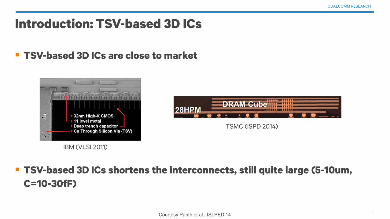
TSV-based 3D ICs are close to market
TSV-based 3D ICs shortens the interconnects, still quite large (5-10um,
C=10-30fF)
Introduction: TSV-based 3D ICs
IBM (VLSI 2011)
TSMC (ISPD 2014)
Courtesy Panth et al., ISLPED’14

9
QUALCOMM RESEARCH
3D VLSI - An Emerging 3D Technology
3D VLSI SRAM
Samsung (2010)
Vertical via
Gate
3D VLSI for general
logic LETI (2011)
High quality thin silicon
(single crystal)
Courtesy Panth et al., ISLPED’14

10
QUALCOMM RESEARCH
3D VLSI: Face-to-Back Fabrication Process
Bottom tier is created as usual Thin Si layer is attached
Fabricate top-tier devices + interconnectsCourtesy Panth et al., ISLPED’14

11
QUALCOMM RESEARCH
3D VLSI: Face-to-Face Fabrication Process

12
QUALCOMM RESEARCH
Transistor-level [1]
Each standard cell is folded
Pin density increases significantly
Footprint reduction is ~40%, not 50%
Standard cell re-design required
CELONCEL [2]
Gate-level, but cell redesign required
Simplified design flow
Same disadvantages as transistor-level
Design Styles Available in 3D VLSI (1/2)
NOR INV NORMIV
[1] Y.-J. Lee, D. Limbrick and S. K. Lim, “Power Benefit Study for Ultra-High Density Transistor-Level Monolithic 3D ICs,” DAC, 2013.
[2] S Bobba et al., “CELONCEL: Effective Design Technique for 3-D Monolithic Integration targeting High Performance Integrated Circuits,” ASPDAC, 2011.
Courtesy Panth et al., ISLPED’14
13
QUALCOMM RESEARCH
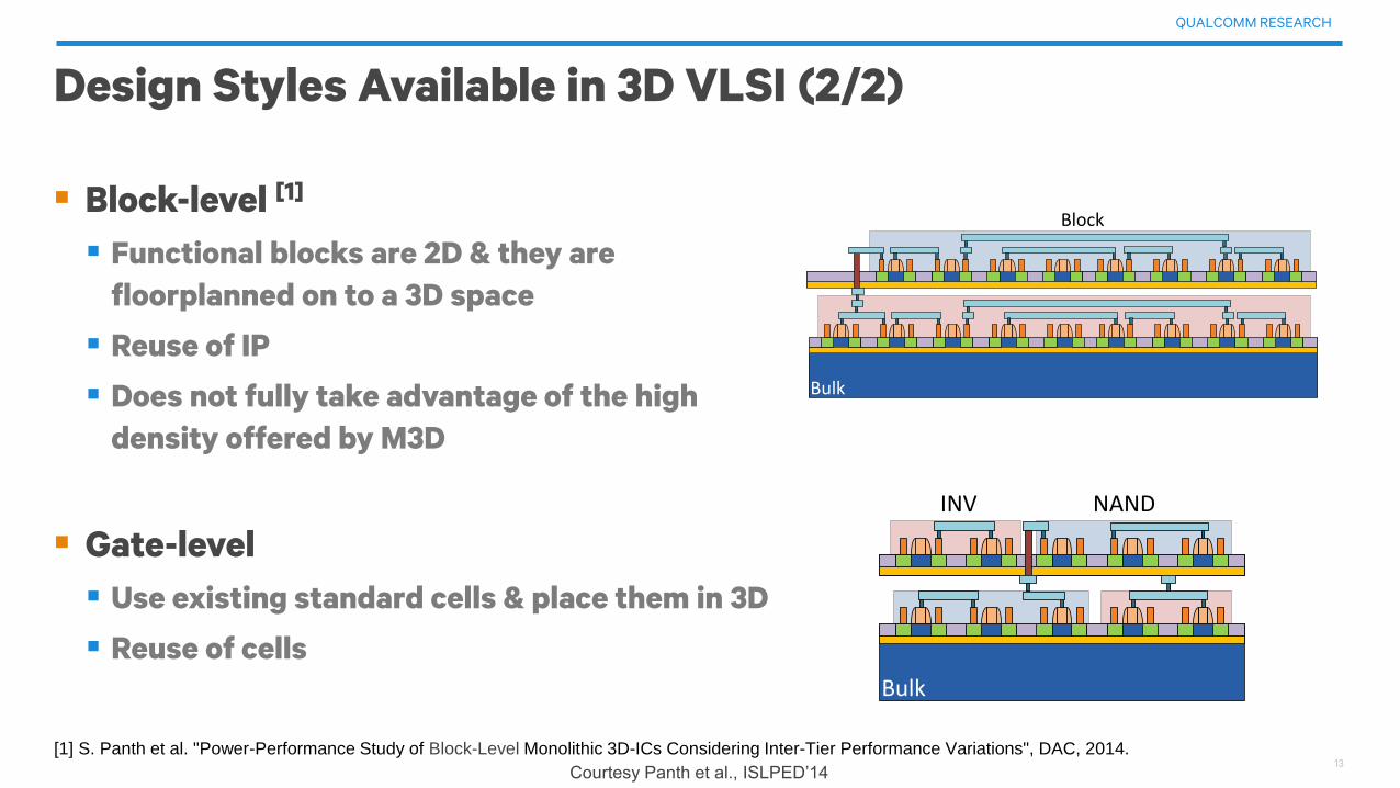
Block-level [1]
Functional blocks are 2D & they are
floorplanned on to a 3D space
Reuse of IP
Does not fully take advantage of the high
density offered by M3D
Gate-level
Use existing standard cells & place them in 3D
Reuse of cells
Design Styles Available in 3D VLSI (2/2)
INV NAND
Bulk
Bulk
Block
[1] S. Panth et al. "Power-Performance Study of Block-Level Monolithic 3D-ICs Considering Inter-Tier Performance Variations", DAC, 2014.
Courtesy Panth et al., ISLPED’14
14
Block-Level 3D VLSI Physical Implementation

15
QUALCOMM RESEARCH
Process improvement: < 625C without performance loss still too high for Cu
interconnect
Preventing damage to interconnects – Two options:
Use Tungsten (W) on the bottom tier Worse interconnects on bottom tier
– Identical devices on both tiers
~ 450C processing on the top tier Worse transistors on the top tier
– Identical interconnects on both tiers
Sequential 3D: Source of Inter-Tier Performance Variation
FEOL processing of top tier
RTA at 1200C will damage both
devices and interconnects
Courtesy Panth et al., DAC’14
16
QUALCOMM RESEARCH
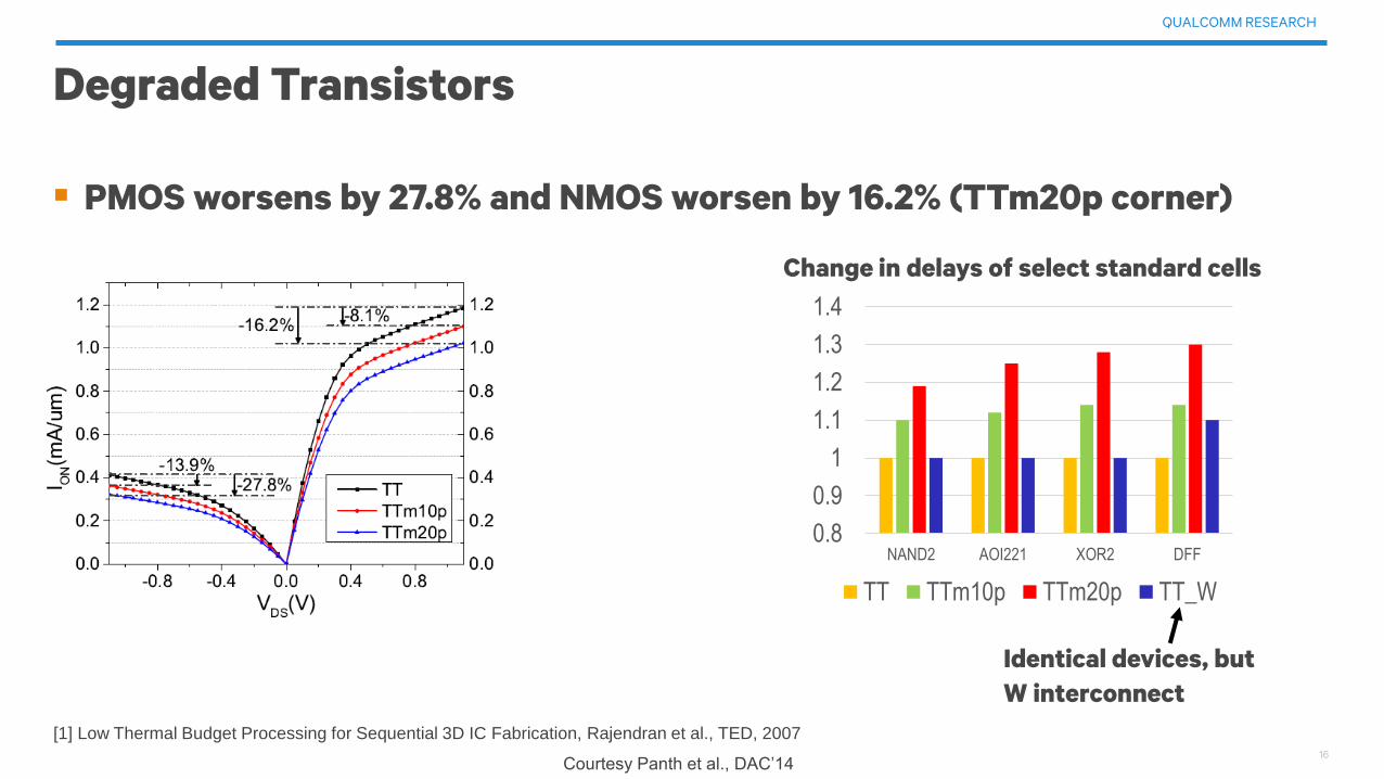
PMOS worsens by 27.8% and NMOS worsen by 16.2% (TTm20p corner)
Degraded Transistors
0.8
0.9
1
1.1
1.2
1.3
1.4
NAND2 AOI221 XOR2 DFF
TT TTm10p TTm20p TT_W
Change in delays of select standard cells
Identical devices, but
W interconnect
[1] Low Thermal Budget Processing for Sequential 3D IC Fabrication, Rajendran et al., TED, 2007
Courtesy Panth et al., DAC’14

17
QUALCOMM RESEARCH
Design Flow
Synthesis
Floorplanning
Vertical Via Planning
P&R of all blocks/tiersDerive WLM
3D Timing and Power
Analysis
RTL
GDSIIFeedback loop
Final signoff analysis
Determine block pin and vertical via locations
Determine the block outlines in a 3D space
Courtesy Panth et al., DAC’14

18
QUALCOMM RESEARCH
Variation-Aware 3D Block-Level Floorplanning
Block Timing Constraints
Block RTL
Normal/Degraded Libraries
Cu/W WLM
Block Synthesis
TTm10pTT TTm20p TT_W
Perturb Solution
3D Move ?
Yes
No
Update Block Area
and Delay Cost
Block flavors
Performance-aware floorplanner
Courtesy Panth et al., DAC’14

19
QUALCOMM RESEARCH
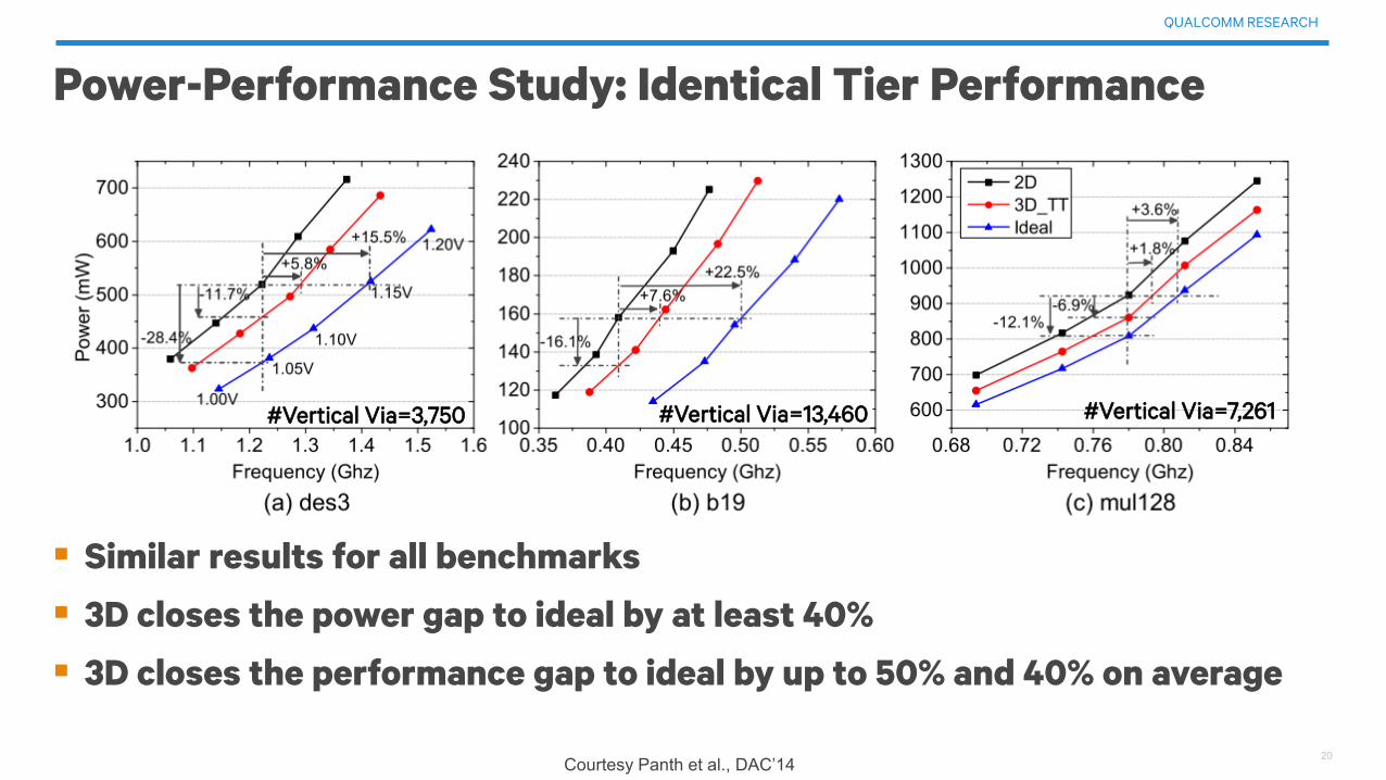
Ideal: Zero RC for inter-block nets: Best possible block-level implementation
Power-Performance Study: Identical Tier Performance
des3 benchmark
M3D closes 37% of
the performance gap
to ideal
M3D closes 41% of the
power gap to ideal
Courtesy Panth et al., DAC’14
20
QUALCOMM RESEARCH
Similar results for all benchmarks
3D closes the power gap to ideal by at least 40%
3D closes the performance gap to ideal by up to 50% and 40% on average
Power-Performance Study: Identical Tier Performance
#Vertical Via=3,750 #Vertical Via=13,460 #Vertical Via=7,261
Courtesy Panth et al., DAC’14

21
QUALCOMM RESEARCH
Dashed lines = no variation-aware floorplanning
Solid lines = variation-aware floorplanning
Variation-Aware Power-Performance Results
Courtesy Panth et al., DAC’14

22
QUALCOMM RESEARCH
Variation-aware floorplanning always gives better results
W on the bottom tier seems to be the best option
Variation-Aware Power-Performance Results
Courtesy Panth et al., DAC’14

23
QUALCOMM RESEARCH
Summary of Results
1 1 1
1.15
5
1.22
5
1.03
6
1.05
8
1.07
6
1.01
8
1.03
1.03
9
1.01
80.97
4
0.97
1
11.04
7
1.07
6
1.01
8
0.9
0.95
1
1.05
1.1
1.15
1.2
1.25
des3 b19 mul128
Nor
mal
izat
ion
1 1 1
0.71
6
0.87
9
0.88
3
0.83
9
0.93
1
0.92
2
0.92
1
0.96
8
1.05
4
1.1
1
0.89
4
0.86 0.
962
0.6
0.7
0.8
0.9
1
1.1
1.2
des3 b19 mul128
Nor
mal
izat
ion
Iso-power frequency
Iso-frequency power
3D closes a significant
portion of the gap to ideal
W interconnects have
marginal overhead
Courtesy Panth et al., DAC’14

24
Gate-Level 3D VLSI Physical Implementation

25
QUALCOMM RESEARCH
Placement-driven partitioning using academic placers [1]
Initial Work in Gate-level 3D VLSI
First, make the 3D footprint 50% of 2D
In a 2D placer, double the placement
capacity of each global bin (for two-tier)
[1] S. Panth et. al., "Placement-Driven Partitioning for Congestion Mitigation in Monolithic 3D IC Designs“, ISPD, 2014.
Partition the design, maintaining local area
balance within each partitioning bin
“Placement-driven Partitioning”
Partitioning bin
Courtesy Panth et al., ISLPED’14

26
QUALCOMM RESEARCH
In a commercial tool, we cannot “double” the supply.
Instead, we first halve the std. cell areas (multiply W/H by 0.707)
“Shrunk 2D” Placement using a Commercial Tool
Original 2D
Std. Cells
Shrunk 2D
Std. Cells
W = 0.707 * W2D
Shrunk 2D Placement Cell Expansion Placement-driven Partitioning
Note: We do not touch the .lib file Timing information is maintained
Courtesy Panth et al., ISLPED’14

27
QUALCOMM RESEARCH
Memory is usually pre-placed before placement starts
We cannot simply superimpose them before feeding it to the commercial
tool for shrunk 2D P&R
Handling Memory Macros: Issues
Tier 0 Tier 1
This will cause a placement blockage in these
regions, which is wrong
Shrunk 2D FootprintCourtesy Panth et al., ISLPED’14

28
QUALCOMM RESEARCH
Memory macros can be thought of as a combination of a placement
blockage and memory pins
If we can isolate each component, then they can be handled separately
during shrunk 2D P&R
Handling Memory Macros: Decomposition
Courtesy Panth et al., ISLPED’14
29
QUALCOMM RESEARCH
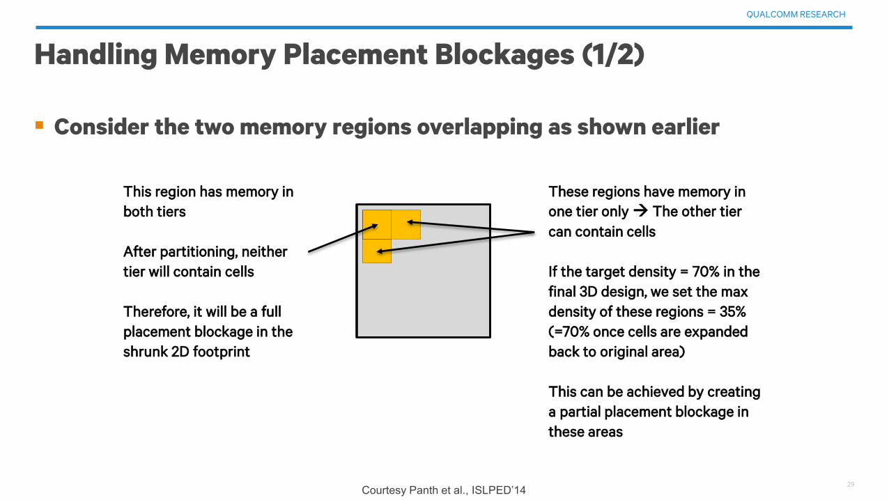
Consider the two memory regions overlapping as shown earlier
Handling Memory Placement Blockages (1/2)
This region has memory in
both tiers
After partitioning, neither
tier will contain cells
Therefore, it will be a full
placement blockage in the
shrunk 2D footprint
These regions have memory in
one tier only The other tier
can contain cells
If the target density = 70% in the
final 3D design, we set the max
density of these regions = 35%
(=70% once cells are expanded
back to original area)
This can be achieved by creating
a partial placement blockage in
these areas
Courtesy Panth et al., ISLPED’14

30
QUALCOMM RESEARCH
Handling Memory Placement Blockages (2/2)
Partial Blockage
Pre-Placed Memory
Projected Memory
Locations
Tier 0
Tier 1
Full Blockage
Pre-placed Memory
Memory Projection Memory Blockage Extraction
Courtesy Panth et al., ISLPED’14

31
QUALCOMM RESEARCH
Design Flow Screenshots
Tier 0
Pre-Placed Memory
Partial
Blockage
Reduced Placement Density
over partial blockages
Full
Blockage
Memory Pins
Tier 1
Memory Projection Shrunk 2D P&R
Tier Partitioning
Courtesy Panth et al., ISLPED’14

32
QUALCOMM RESEARCH
Design Flow
Placement
Pre-CTS Optimization
CTS
Post-CTS Optimization
Routing
Post-route Optimization
Tier Partitioning
Tier-by-tier Route
3D Timing & Power Analysis
MIV/F2F Insertion
Tier-by-tier RC Extraction
Shrunk 2D
Courtesy Panth et al., ISLPED’14

33
QUALCOMM RESEARCH
Consider two cells connected to each other in Shrunk 2D & then in 3D
But LMIV < 1um. Therefore LS2D ≈ L3D
However, the wire widths are different; WS2D = 0.707 W3D
Since we want RS2D ≈ R3D and CS2D ≈ C3D, we do not scale the per-unit-
length RC values in the cap table file for shrunk 2D design.
Matching Wire Parasitics between Shrunk 2D and 3D
LS2D = Lx + Ly L3D = Lx + Ly + LMIV
Courtesy Panth et al., ISLPED’14
34
QUALCOMM RESEARCH
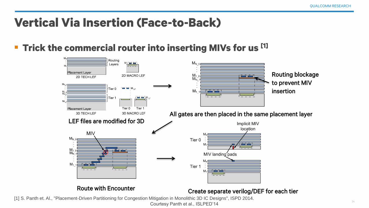
Trick the commercial router into inserting MIVs for us [1]
Vertical Via Insertion (Face-to-Back)
[1] S. Panth et. Al., "Placement-Driven Partitioning for Congestion Mitigation in Monolithic 3D IC Designs", ISPD 2014.
LEF files are modified for 3D All gates are then placed in the same placement layer
Routing blockage
to prevent MIV
insertion
Route with EncounterCreate separate verilog/DEF for each tier
Courtesy Panth et al., ISLPED’14

35
QUALCOMM RESEARCH
Vertical Via Insertion (Face-to-Face)
LEF files are modified for 3D All gates are then placed in the same placement layer
Reverse the order of
metals in Tier 0
Do not add any routing
blockage to prevent F2F
insertion over cells
Courtesy Panth et al., ISLPED’14

36
QUALCOMM RESEARCH
F2B / F2F MIV Insertion Screenshots
F2B MIV
F2F MIV
Courtesy Panth et al., ISLPED’14

37
QUALCOMM RESEARCH
Conventional 3D flows have a tier-by-tier optimization step
It is very difficult to derive timing budgets for multiple MIVs per net
Shrunk 2D flow enables multiple MIV insertion Lower WL and power
Single vs. Multiple MIV Insertion: Screenshots
Tier0 Multiple MIVs
Single 3D connection
Tier1
Tier0
Tier1
Single MIV Insertion Multiple MIV Insertion
Courtesy Panth et al., ISLPED’14

38
QUALCOMM RESEARCH
Single vs. Multiple Vertical Via Insertion: Results
F2B 3D F2F 3D
Single Multiple Single Multiple
Total WL (m) 15.61 14.29 (-8.43%) 15.44 13.89 (-10.05%)
#MIV/F2F 106k 235k (+120.44%) 106k 202k (+89.72%)
Total Power (mW) 534.10 522.10 (-2.25%) 538.30 524.00 (-2.66%)
Cell Power (mW) 126.90 126.10 (-0.63%) 127.30 126.40 (-0.71%)
Net Power (mW) 293.90 282.70 (-3.81%) 297.80 284.30 (-4.53%)
Leak. Power (mW) 113.30 113.30 (+0.0%) 113.30 113.30 (0.00)
Courtesy Panth et al., ISLPED’14

39
QUALCOMM RESEARCH
3D Clock-Tree Synthesis
Clock Buffer
Flip-flop
Tier 0
Tier 0 Tier 1
3D Net
Clock gate
Tier 0 Tier 1
Tier 0
Traditional 3D CTS: Source-level
One clock-tree per clock-gating group
in each tier, tied together at the root
level
Proposed 3D CTS: Leaf-level
Keep the entire backbone on one tier.
Only insert clock MIVs to connect the
FF on different tiers at the leaf level
Courtesy Panth et al., ISLPED’14

40
QUALCOMM RESEARCH
Leaf-Level CTS: Screenshots
Clock MIV
Leaf clock net
Flip-Flop
Clock backbone
Leaf buffer
Clock back-bone on Tier 0
Leaf clock
net on Tier 0
Leaf clock
net on Tier 1
Zoom in of red rectangle
Courtesy Panth et al., ISLPED’14
41
QUALCOMM RESEARCH
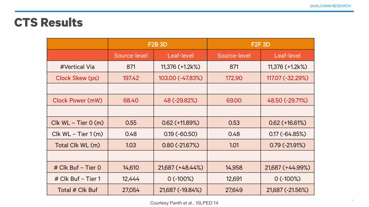
CTS Results
F2B 3D F2F 3D
Source-level Leaf-level Source-level Leaf-level
#Vertical Via 871 11,376 (+1.2k%) 871 11,376 (+1.2k%)
Clock Skew (ps) 197.42 103.00 (-47.83%) 172.90 117.07 (-32.29%)
Clock Power (mW) 68.40 48 (-29.82%) 69.00 48.50 (-29.71%)
Clk WL – Tier 0 (m) 0.55 0.62 (+11.89%) 0.53 0.62 (+16.61%)
Clk WL – Tier 1 (m) 0.48 0.19 (-60.50) 0.48 0.17 (-64.85%)
Total Clk WL (m) 1.03 0.80 (-21.67%) 1.01 0.79 (-21.91%)
# Clk Buf – Tier 0 14,610 21,687 (+48.44%) 14,958 21,687 (+44.99%)
# Clk Buf – Tier 1 12,444 0 (-100%) 12,691 0 (-100%)
Total # Clk Buf 27,054 21,687 (-19.84%) 27,649 21,687 (-21.56%)
Courtesy Panth et al., ISLPED’14

42
QUALCOMM RESEARCH
Single Vt Power Comparisons (mW)
Encounter 2D Shrunk 2D F2B 3D F2F 3D
Total 618.40 514.40 (-16.82%) 522.10 (-15.57%) 524.00 (-15.27%)
Cell 135.60 126.80 (-6.49%) 126.10 (-7.01%) 126.40 (-6.78%)
Net 356.30 274.30 (-23.01%) 282.70 (-20.66%) 284.30 (-20.21%)
Leakage 126.50 113.30 (-10.43%) 113.30 (-10.43%) 113.30 (-10.43%)
Memory 49.00 45.10 (-7.96%) 45.10 (-7.96%) 45.00 (-8.16%)
Combinational 385.10 300.00 (-22.10%) 305.30 (-20.72%) 306.80 (-20.33%)
Clock Tree 62.50 46.90 (-24.96%) 48.00 (-23.20%) 48.50 (-22.40%)
Courtesy Panth et al., ISLPED’14

43
QUALCOMM RESEARCH
Dual Vt Power Comparisons (mW)
Encounter 2D Shrunk 2D F2B 3D F2F 3D
Total 572.10 471.4 (-17.60%) 480.10 (-16.08%) 482.20 (-15.71%)
Cell 131.80 122.5 (-7.06%) 123.00 (-6.68%) 123.30 (-6.45%)
Net 356.60 274.2 (-23.11%) 282.70 (-20.72%) 284.30 (-20.27%)
Leakage 83.60 74.7 (-10.65%) 74.70 (-11.00%) 74.60 (-10.77%)
Memory 48.80 45.1 (-7.58%) 45.10 (-7.58%) 45.00 (-7.79%)
Combinational 361.60 278.6 (-22.95%) 283.00 (-21.74%) 284.30 (-21.38%)
Clock Tree 62.50 47.3 (-24.32%) 48.00 (-23.20%) 48.50 (-22.40%)
Courtesy Panth et al., ISLPED’14

44
Thermal Implications of 3D ICs

45
QUALCOMM RESEARCH
Compact model derived from full system cellphone model
SoC temperature matched with full system model
Thermal Model Setup – Die, Package and Cooling Mechanism
Typical Mobile Full System Thermal Model Compact Model
(SoC Package, board and top side heat spreader only)

46
QUALCOMM RESEARCH
3D stack-up for Face-to-Face (F2F) and Face-to-Back (F2B)
Back-End-Of-Line (BEOL) modeled as one layer with effective thermal properties
Tier 2 Silicon with vertical connections modeled as one layer with effective thermal
properties
Thermal Model Setup – F2B and F2F Stack up
(a) F2B stack-up (b) F2F stack-up
Mold
Package Substrate
Tier 1 silicon

47
QUALCOMM RESEARCH
Model Generation – Power Mapping
2D and 3D silicon areas are similar ~ 50% area footprint shrink
1x1 mm2 squares 100 mm2 2D design

48
QUALCOMM RESEARCH
Model Generation – Simulation Methodology
Influence coefficient methodology
∆𝑇 = 𝐻𝑖𝑗 × 𝑃𝑖
Temperature-dependent leakage power loop

49
QUALCOMM RESEARCH
ICM based solver data compared with simulation using commercial
thermal analysis tool, ICEPAK
Temperature delta (ICM- ICEPAK) = 0.2˚C
Excellent match achieved between finite-volume analysis vs. ICM method
ICM Model Accuracy
SoC Temperature distribution SoC Temperature Difference

50
QUALCOMM RESEARCH
Power input: power distribution for a typical quad-core CPU case
Results: Temperature difference between tiers is small < 1˚C
Distance between tiers is very small small thermal resistance between tiers good
mutual heating
Power is low on each tier: ΔT = R x P
3D Thermal Characteristics
Dynamic Power Distribution

51
QUALCOMM RESEARCH
Power input: power distribution for a typical quad-core CPU case
F2F integration is slightly hotter than F2B (~ 1˚C)
In F2F, the active layers are closer to each other
In F2B there is a layer of thin silicon between the two tiers which slightly helps with
temperature reduction
3D Thermal Characteristics – F2B vs. F2F Integration
Dynamic Power Distribution

52
QUALCOMM RESEARCH
With the same power inputs, 3D temperature is higher than 2D
3D temperature is very sensitive to IP block partitioning
Non-staggered partitioning results is higher junction temperatures, requiring 16% power
reduction in 3D to match 2D
With only 5% power reduction in staggered partitioning, 3D temperature matches with 2D
Temperature Rise in 3D vs. 2D: IP Block Partitioning Impact
Dynamic Power Distribution (W) Temperature Distribution (˚C)
(a) Baseline 2D, (b) Staggered and (c) Non-staggered designs

53
QUALCOMM RESEARCH
3D thermal risk is lower if the high power density is placed in the center of the die
Temperature rise is significantly lower for center IP block (96.2C vs. 88.8C)
Power saving requirement is the same for both floorplans
~5% for staggered partitioning
~16% for non-staggered partitioning
Power saving is more sensitive to partitioning than floorplanning
Temperature Rise in 3D vs. 2D: Floorplanning Impact
corner hotspot scenario center hotspot scenario

54
QUALCOMM RESEARCH
Power savings are primarily coming from wirelength and buffer reductions
𝑃𝑡𝑜𝑡𝑎𝑙 = 𝑝𝑖𝑛𝑡𝑒𝑟𝑛𝑎𝑙 + 𝑝𝑠𝑤𝑖𝑡𝑐ℎ𝑖𝑛𝑔 + 𝑝𝑙𝑒𝑎𝑘𝑎𝑔𝑒
𝑝𝑠𝑤𝑖𝑡𝑐ℎ𝑖𝑛𝑔3𝐷 = 𝛼 ∙ 𝑐𝑝𝑖𝑛 + 𝛽 ∙ 𝑐𝑤𝑖𝑟𝑒 ∙ 𝑝𝑠𝑤𝑖𝑡𝑐ℎ𝑖𝑛𝑔
2𝐷
Internal and leakage components are proportional to total cell area
Power Saving Opportunities in 3D

55
QUALCOMM RESEARCH
(a) 2D block partitioning with 2D
floorplanning
(b) 2D block partitioning with 3D
floorplanning
(c) 3D block partitioning with 2D
floorplanning
(d) Combination of 2D and 3D block
partitioning with 3D floorplanning
Floorplanning and Partitioning Options in 3D

56
QUALCOMM RESEARCH
3D Floorplanning and Partitioning Case Study: GPU Power
Intensive Case
Thermal maps of mobile MPSoC GPU intensive use-case for (a) 2D, (b) All 3D and (c) All 2D configurations

57
QUALCOMM RESEARCH
3D Floorplanning and Partitioning Case Study: CPU Power
Intensive Case
Thermal maps of mobile MPSoC CPU intensive use-case for (a) 2D, (b) All 3D, and (c) All 2D configurations
58
QUALCOMM RESEARCH
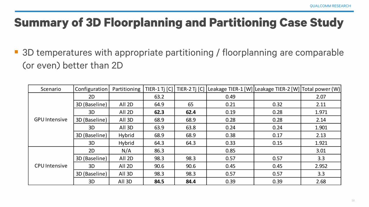
3D temperatures with appropriate partitioning / floorplanning are comparable
(or even) better than 2D
Summary of 3D Floorplanning and Partitioning Case Study
Scenario Configuration Partitioning TIER-1 Tj [C] TIER-2 Tj [C] Leakage TIER-1 [W] Leakage TIER-2 [W] Total power (W)
2D 63.2 0.49 2.07
3D (Baseline) All 2D 64.9 65 0.21 0.32 2.11
3D All 2D 62.3 62.4 0.19 0.28 1.971
3D (Baseline) All 3D 68.9 68.9 0.28 0.28 2.14
3D All 3D 63.9 63.8 0.24 0.24 1.901
3D (Baseline) Hybrid 68.9 68.9 0.38 0.17 2.13
3D Hybrid 64.3 64.3 0.33 0.15 1.921
2D N/A 86.3 0.85 3.01
3D (Baseline) All 2D 98.3 98.3 0.57 0.57 3.3
3D All 2D 90.6 90.6 0.45 0.45 2.952
3D (Baseline) All 3D 98.3 98.3 0.57 0.57 3.3
3D All 3D 84.5 84.4 0.39 0.39 2.68
GPU Intensive
CPU Intensive

59
QUALCOMM RESEARCH
Practical and cost efficient 3DVLSI technologies are emerging
A new generation of implementation tools are required to take full
advantage of 3DVLSI technology
Floorplanner
Place & Route
Extraction
Timing
CTS
New design methodologies are required
New Architectures
New foundation IP structures
Conclusions
Courtesy Saeidi et al., 3DIC’14

60
All data and information contained in or disclosed by this document is confidential and proprietary information of Qualcomm Technologies, Inc. and all rights therein
are expressly reserved. By accepting this material the recipient agrees that this material and the information contained ther ein is to be held in confidence and in trust
and will not be used, copied, reproduced in whole or in part, nor its contents revealed in any manner to others without the e xpress written permission of Qualcomm
Technologies, Inc.
© 2013 QUALCOMM Incorporated and/or its subsidiaries. All Rights Reserved.
Qualcomm is a trademark of Qualcomm Incorporated, registered in the United States and other countries.
Other products and brand names may be trademarks or registered trademarks of their respective owners
References in this presentation to “Qualcomm” may mean Qualcomm Incorporated, Qualcomm Technologies, Inc., and/or other subsi diaries or business units within the
Qualcomm corporate structure, as applicable.
Qualcomm Incorporated includes Qualcomm’s licensing business, QTL, and the vast majority of its patent portfolio. Qualcomm Te chnologies, Inc., a wholly-owned
subsidiary of Qualcomm Incorporated, operates, along with its subsidiaries, substantially all of Qualcomm’s engineering, rese arch and development functions, and
substantially all of its product and services businesses,
including its semiconductor business.
Thank you
Qualcomm Research
www.qualcomm.com/research
Related Documents