Sherwood Parker (U. of Hawaii) Collaborators: High Energy Physics Projects C. Kenney * (Molecular Biology Consortium) C. Da Via, J. Hasi *, A. Kok, S. Watts (Brunel University) S. Seidel, M. Hoeferkamp, I. Gorelov (University of New Mexico) Members of the TOTEM, Czech Technical Univ. and FP420 groups Kevin Einsweiler, Maurice Garcia-Sciveres (LBL) G. Anelli, P. Jarron, M. Despeisse (CERN – Microelectronics group) J. Morse (European Synchrotron Radiation Facility), E. Perozziello * Collaborators: Structural Molecular Biology

3D sensors Sherwood Parker (U. of Hawaii) Collaborators: High Energy Physics Projects C. Kenney * (Molecular Biology Consortium) C. Da Via, J. Hasi *,
Dec 25, 2015
Welcome message from author
This document is posted to help you gain knowledge. Please leave a comment to let me know what you think about it! Share it to your friends and learn new things together.
Transcript
3D sensorsSherwood Parker (U. of Hawaii)
Collaborators: High Energy Physics Projects
C. Kenney * (Molecular Biology Consortium)
C. Da Via, J. Hasi *, A. Kok, S. Watts (Brunel University)
S. Seidel, M. Hoeferkamp, I. Gorelov (University of New Mexico)
Members of the TOTEM, Czech Technical Univ. and FP420 groups
Kevin Einsweiler, Maurice Garcia-Sciveres (LBL)
G. Anelli, P. Jarron, M. Despeisse (CERN – Microelectronics group)
J. Morse (European Synchrotron Radiation Facility), E. Perozziello
* Collaborators: Structural Molecular BiologyE. Westbrook, A. Thompson (MBC), D. Gnani (LBL)
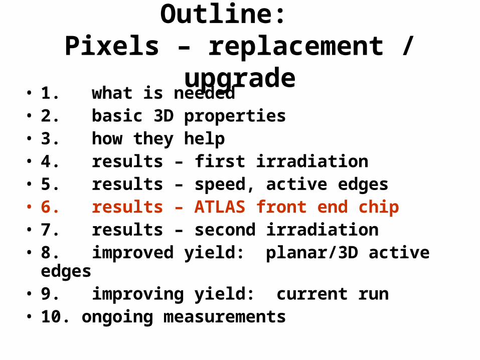
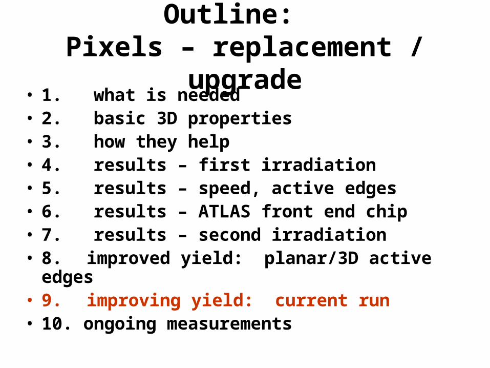
Outline: Pixels – replacement / upgrade
• 1. what is needed• 2. basic 3D properties• 3. how they help• 4. results – first irradiation• 5. results – speed, active edges• 6. results – ATLAS front end chip• 7. results – second irradiation• 8. improved yield: planar/3D active edges• 9. improving yield: current run• 10. ongoing measurements

From:B-Layer Replacement Proposal, Goals
K. Einsweiler, LBNLDecember Pixel Week, 2004
Scope:
•Therefore propose that new B-layer have design goal of 3 times design luminosity both for total dose lifetime and for instantaneous luminosity tolerance. For total dose, assume that a similar several year lifetime is needed, so this would translate to about 3 x 10¹⁵ n equivalent NIEL dose and 150 MRad ionizing dose.
•Of course if this proves too difficult, we can always build several B-Layers using the present technology, and change them each year or two.
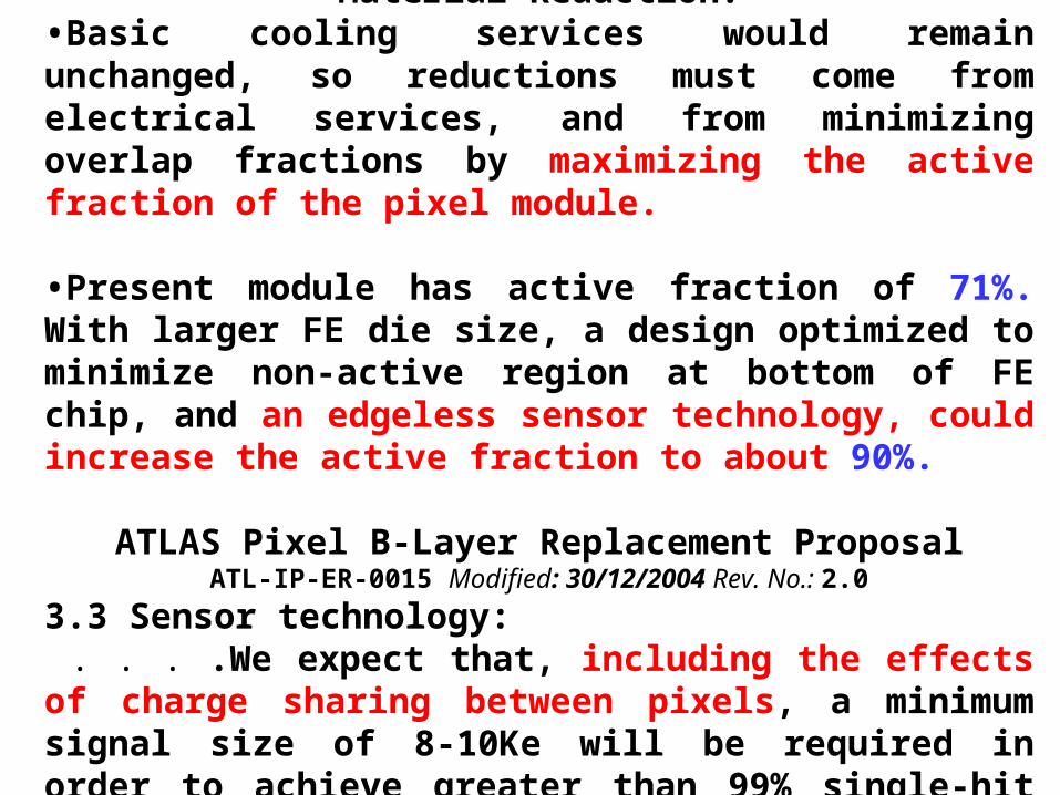
Material Reduction:•Basic cooling services would remain unchanged, so reductions must come from electrical services, and from minimizing overlap fractions by maximizing the active fraction of the pixel module.
•Present module has active fraction of 71%. With larger FE die size, a design optimized to minimize non-active region at bottom of FE chip, and an edgeless sensor technology, could increase the active fraction to about 90%.
ATLAS Pixel B-Layer Replacement ProposalATL-IP-ER-0015 Modified: 30/12/2004 Rev. No.: 2.0
3.3 Sensor technology: . . . .We expect that, including the effects of charge sharing between pixels, a minimum signal size of 8-10Ke will be required in order to achieve greater than 99% single-hit efficiency for the B-Layer.

Outline: Pixels – replacement / upgrade
• 1. what is needed• 2. basic 3D properties• 3. how they help• 4. results – first irradiation• 5. results – speed, active edges• 6. results – ATLAS front end chip• 7. results – second irradiation• 8. improved yield: planar/3D active edges• 9. improving yield: current run• 10. ongoing measurements

3D silicon detectors were proposed in 1995 by S. Parker, and active edges in 1997 by C. Kenney.
Combine traditional VLSI processing andMEMS (Micro Electro Mechanical Systems)technology.
Electrodes are processed inside the detectorbulk instead of being implanted on the Wafer's surface.
The edge is an electrode! Dead volume at the Edge < 2 microns! Essential for -Large area coverage-Forward physics
INTRODUCTION INTRODUCTION
1. NIMA 395 (1997) 328 2. IEEE Trans Nucl Sci 46 (1999) 12243. IEEE Trans Nucl Sci 48 (2001) 1894. IEEE Trans Nucl Sci 48 (2001) 1629 5. IEEE Trans Nucl Sci 48 (2001) 2405 6. CERN Courier, Vol 43, Jan 2003, pp 23-
267. NIMA 509 (2003)86-918. NIMA 524 (2004) 236-244
p
n
100 µm
134 µm
p
200 µm
100 µm
n
nn
n
n n
n
(sig
nal
str
eng
th f
rom
infr
a re
d li
gh
t b
eam
)
+
n-type bulk

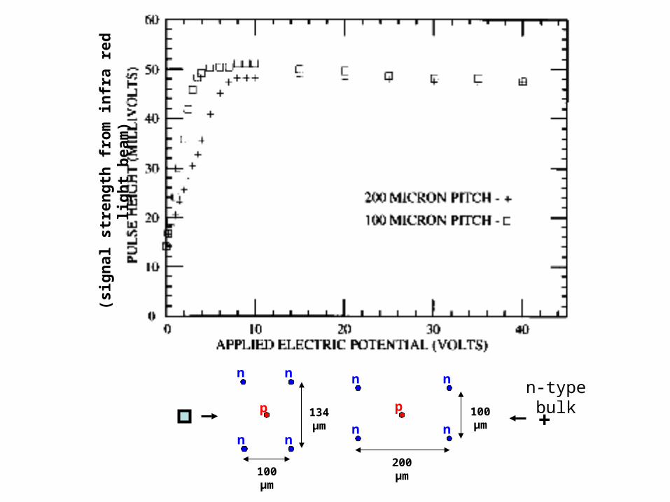
1. 3D lateral cell size can be smaller than wafer thickness, so
2. in 3D, field lines end on cylinders rather than on circles, so
3. most of the signal is induced when the charge is close to theelectrode, where the electrode solid angle is large, so planarsignals are spread out in time as the charge arrives, and
4. Landau fluctuations along track arrive sequentially and may cause secondary peaks (see next slide)
5. if readout has inputs from both n+ and p+ electrodes,
6. for long, narrow pixels and fast electronics,
Speed: planar 3D
1. shorter collection distance
2. higher average fields for any given maximum field (price: larger electrode capacitance)
3. 3D signals are concentrated in time as the track arrives
4. Landau fluctuations arrive nearly simultaneously
5. drift time corrections can be made
6. track locations within the pixel can be found
4.
4.
4.

Potential 3D features from preliminary calculations:
3. Fast pulses. Current to the p electrode and the other 3 n electrodes.
(The track is parallel to the electrodes through a cell center and a null point. V – bias = 10V. Cell centers are in center of any quadrant. Null points are located between pairs of n electrodes.)
1 ns 3 ns
50 µm
p
n
8 µm50 µm

Outline: Pixels – replacement / upgrade
• 1. what is needed• 2. basic 3D properties• 3. how they help• 4. results – first irradiation• 5. results – speed, active edges• 6. results – ATLAS front end chip• 7. results – second irradiation• 8. improved yield: planar/3D active edges• 9. improving yield: current run• 10. ongoing measurements

Useful properties of 3D radiation sensors:
1 Long tracks can have short drift distances.
2 They can be depleted, and have full sensitivity, at lower bias voltages.
3 The geometric nature of this means there will be a low increase of depletion voltage with radiation damage.
4 They have rapid charge collection, and charges from perpendicular tracks come in together, rather than one at a time from the track ends, so they can make order-of-magnitude shorter pulses.

5. This speed is maintained, as expected, in heavily irradiated sensors, and is useful in reducing capture losses regardless of amplifier speeds.
6. With fields directed away from, rather than along pixel or strip boundaries, they have reduced charge-sharing.
Charge-sharing may be used to improve spatial resolution, but may also take tracks below threshold in radiation damaged silicon, particularly with planar sensors.

7. Active edges provide full sensitivity to within a few microns of the physical edges, in contrast with the large dead regions of standard planar technology (1.1 mm in the Atlas and CMS pixel sensors which must allow for many concentric guard rings).
8. Bias voltages can be made to vary across 3D sensors. (useful if radiation damage and so depletion voltages are much higher at, for example, sensor edges near the beam)

BUT
they require more fabrication work.

Outline: Pixels – replacement / upgrade
• 1. what is needed• 2. basic 3D properties• 3. how they help• 4. results – first irradiation• 5. results – speed, active edges• 6. results – ATLAS front end chip• 7. results – second irradiation• 8. improved yield: planar/3D active edges• 9. improving yield: current run• 10. ongoing measurements

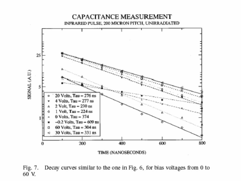
V - bias
Probe point
C - sensorC - probeR - probe

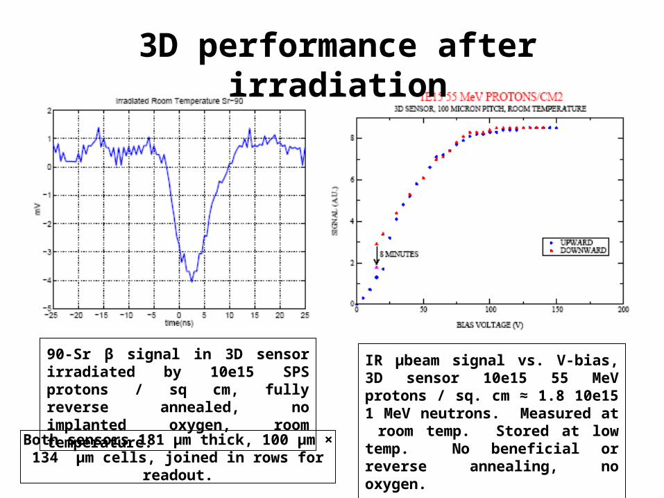
3D performance after irradiation
90-Sr β signal in 3D sensor irradiated by 10e15 SPS protons / sq cm, fully reverse annealed, no implanted oxygen, room temperature.
IR µbeam signal vs. V-bias, 3D sensor 10e15 55 MeV protons / sq. cm ≈ 1.8 10e15 1 MeV neutrons. Measured at room temp. Stored at low temp. No beneficial or reverse annealing, no oxygen.
Both sensors 181 µm thick, 100 µm × 134 µm cells, joined in rows for readout.
Outline: Pixels – replacement / upgrade
• 1. what is needed• 2. basic 3D properties• 3. how they help• 4. results – first irradiation• 5. results – speed, active edges• 6. results – ATLAS front end chip• 7. results – second irradiation• 8. improved yield: planar/3D active edges• 9. improving yield: current run• 10. ongoing measurements

planar sensor pulse shape

rise times ≈ 3.5 ns fall times ≈ 3.5 ns
0.13 µm chips now fabricated – rise, fall times expected to be ≈ 1.5 ns
Resistive (transistor channel) feedback, and so a current amplifier.


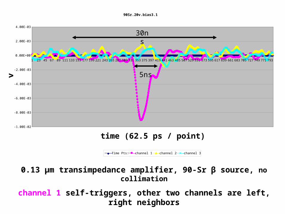
90Sr.20v.bias3.1
-1.00E-02
-8.00E-03
-6.00E-03
-4.00E-03
-2.00E-03
0.00E+00
2.00E-03
4.00E-03
1 23 45 67 89 111 133 155 177 199 221 243 265 287 309 331 353 375 397 419 441 463 485 507 529 551 573 595 617 639 661 683 705 727 749 771 793
time (62.5 ps / point)
v
Time Pts: channel 1 channel 2 channel 3
5ns
30ns
0.13 µm transimpedance amplifier, 90-Sr β source, no collimation
channel 1 self-triggers, other two channels are left, right neighbors

90Sr.20v.bias3.2
-5.00E-03
-4.00E-03
-3.00E-03
-2.00E-03
-1.00E-03
0.00E+00
1.00E-03
2.00E-03
3.00E-03
1 23 45 67 89 111 133 155 177 199 221 243 265 287 309 331 353 375 397 419 441 463 485 507 529 551 573 595 617 639 661 683 705 727 749 771 793
time (62.5 ps / point)
v
Time Pts: channel 1 channel 2 channel 3
5ns
30ns
0.13 µm transimpedance amplifier, 90-Sr β source, no collimationchannel 1 self-triggers, other two channels are left, right neighbors

90Sr.20v.bias3.3
-5.00E-03
-4.00E-03
-3.00E-03
-2.00E-03
-1.00E-03
0.00E+00
1.00E-03
2.00E-03
1 23 45 67 89 111 133 155 177 199 221 243 265 287 309 331 353 375 397 419 441 463 485 507 529 551 573 595 617 639 661 683 705 727 749 771 793
time (62.5 ps / point)
v
Time Pts: channel 1 channel 2 channel 3
5ns
30ns
0.13 µm transimpedance amplifier, 90-Sr β source, no collimationchannel 1 self-triggers, other two channels are left, right neighbors

90Sr.20v.bias3.4
-4.00E-03
-3.00E-03
-2.00E-03
-1.00E-03
0.00E+00
1.00E-03
2.00E-03
1 23 45 67 89 111 133 155 177 199 221 243 265 287 309 331 353 375 397 419 441 463 485 507 529 551 573 595 617 639 661 683 705 727 749 771 793
time (62.5 ps / point)
v
Time Pts: channel 1 channel 2 channel 3
5ns
30ns

-1.20E-02
-1.00E-02
-8.00E-03
-6.00E-03
-4.00E-03
-2.00E-03
0.00E+00
2.00E-03
4.00E-03
1 25 49 73 97 121 145 169 193 217 241 265 289 313 337 361 385 409 433 457 481 505 529 553 577 601 625 649 673 697 721 745 769 793
5ns
Amplifier output, 0.8 ns rise-time step pulse applied to input.
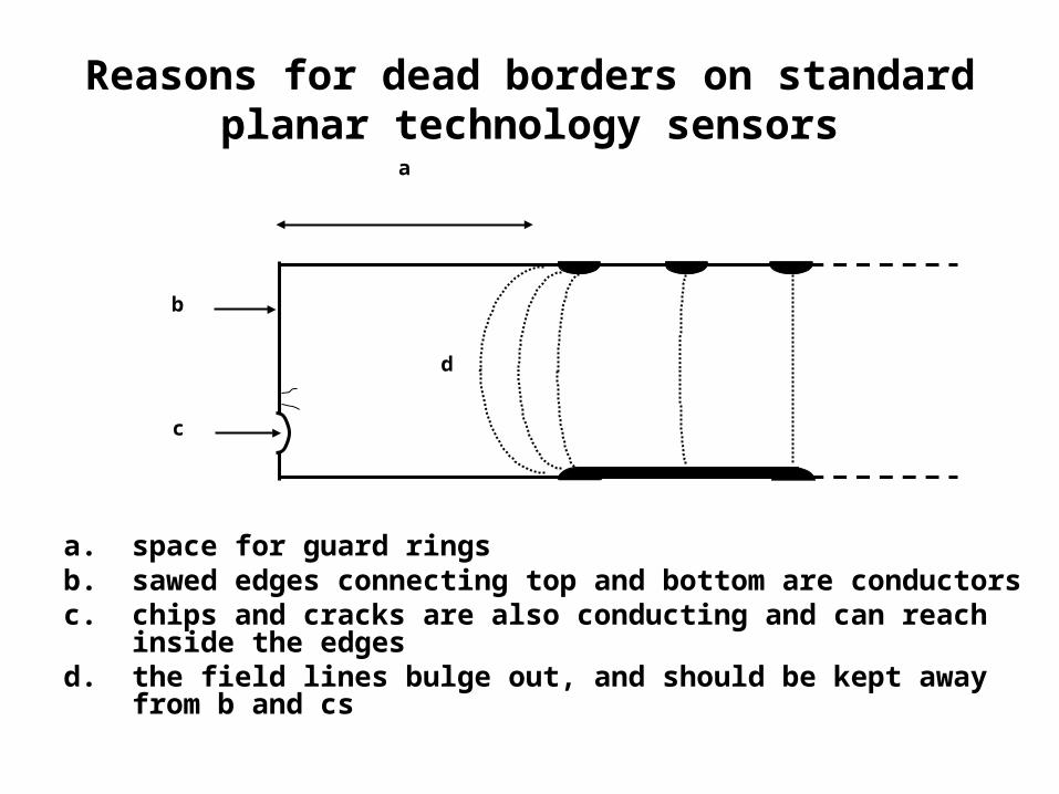
Reasons for dead borders on standard planar technology sensors
a
b
c
d
a. space for guard ringsb. sawed edges connecting top and bottom are conductorsc. chips and cracks are also conducting and can reach inside the
edgesd. the field lines bulge out, and should be kept away from b and
cs

Active Edges
support wafer oxide
sensor wafer
p n n
support wafer oxide
p n
p
n
poxide
1. etch border trenches
2. diffuse in dopant
3. grow protective oxide cover
4. fill trench with poly
5. vertical, directed etch (to dotted lines)
6. turn off sidewall protection step
7. isotropic etch to oxide stop
8. additional steps are not included on this slide (and note, bonding oxide to support wafer not colored )
9. n and p electrodes can be reversed

Some work on deep etching:
1. Process steps to improve depth / diameter ratios, and to make holes and trenches at the same time (middle). Note: s(↕) = s(↔) × cos 20º.
2. True diameter from an angled saw cut: (right). D/d, top holes ≈ 18 / 1.
3. A second, newer STS etcher has just been installed at Stanford. It is faster and should make somewhat narrower holes and trenches.
4. The old etcher will become a “dirty” one, allowing us to make trench “dicing” etches on wafers with indium bumps.
Dd
0. An old hole (filled).
D/d = 121 µm /11µm.

X-ray microbeam results for a 3D sensor
X-ray micro-beam scan, in 2 µm steps, of a 3D, n bulk and edges, 181
µm thick sensor. The left curve is for the edge p channel. The horizontal scale is in µm; the vertical is arbitrary. The small dip in each center is from nearby 3D electrodes. The left edge tail is from reflected gold x-rays and from leakage current.
0
10
20
30
40
0 100 200 300 400
edgeinter-strip
boundaries

0
60
120
180
240
300
360
0918
27
36
45
54
microns
45-54
36-45
27-36
18-27
9-18
0-9
Current from scan in an x-ray microbeam, of another 3D sensor with a photomicrograph of the corresponding part on the right. Grid
lines are spaced 10µm apart.

Some results from the CERN X5 beam test (120 GeV muons)
Measured hit position in 3D sensor plane #3 vs. predicted position from beam telescope.
Fitted 3D sensor width = 3,203 ±4 µm. Drawn width = 3,195 µm. Sensor efficiency = 98%. System efficiency less due to DAQ, triggering electronics.
Outline: Pixels – replacement / upgrade
• 1. what is needed• 2. basic 3D properties• 3. how they help• 4. results – first irradiation• 5. results – speed, active edges• 6. results – ATLAS front end chip• 7. results – second irradiation• 8. improved yield: planar/3D active edges• 9. improving yield: current run• 10. ongoing measurements

More typical spectrum TOT spectrum for the best looking pixel
Possible steps for improvement of fabrication yields:
• Improvement of fabrication steps (as was done for planar / 3D active edge sensors).• Use solder bumps at wafer scale.• 2-3 month fabrication run rather than 5 week run.• Use of P- type bulk so diode junctions always at signal electrodes so one bad junction does not short bias supply.• Probably won’t need to reduce signal electrode capacitance using poly-resistor isolation of bias electrodes, but it remains a possibility.
Outline: Pixels – replacement / upgrade
• 1. what is needed• 2. basic 3D properties• 3. how they help• 4. results – first irradiation• 5. results – speed, active edges• 6. results – ATLAS front end chip• 7. results – second irradiation• 8. improved yield: planar/3D active edges• 9. improving yield: current run• 10. ongoing measurements
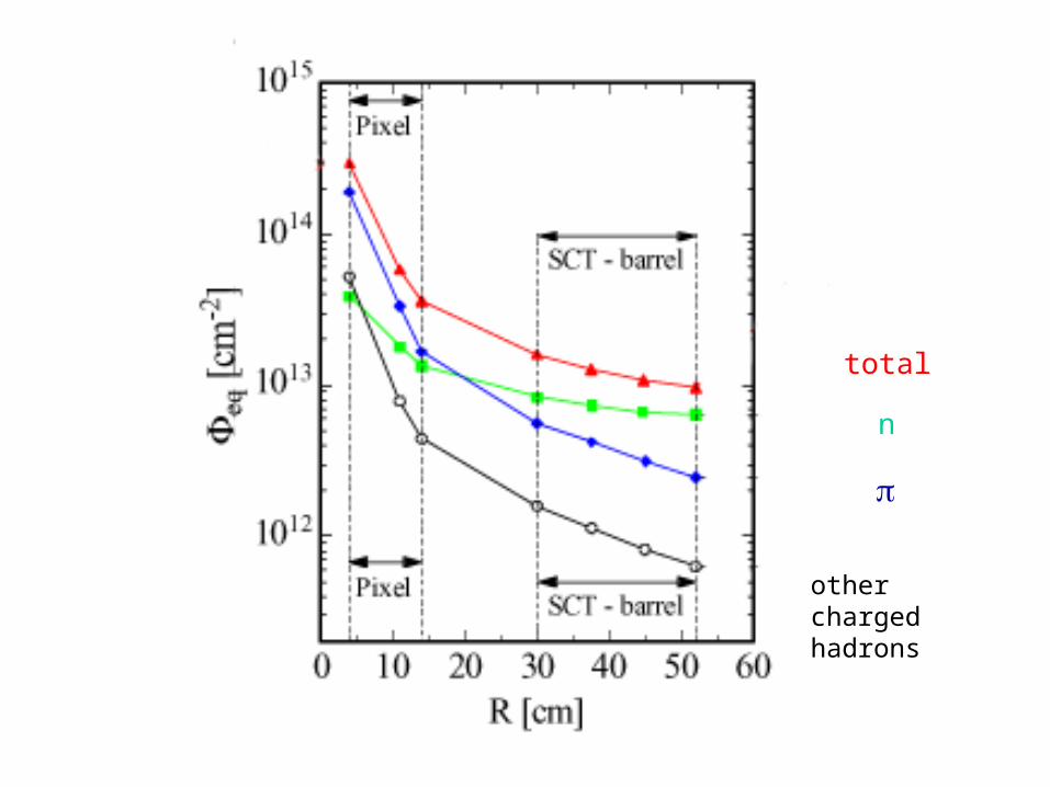
n
otherchargedhadrons
total

Displacement Damage in Silcon for Different Particles
1.0E-05
1.0E-04
1.0E-03
1.0E-02
1.0E-01
1.0E+00
1.0E+01
1.0E+02
1.0E+03
1.0E+04
1.0E-10 1.0E-08 1.0E-06 1.0E-04 1.0E-02 1.0E+00 1.0E+02 1.0E+04
particle energy [MeV]
D/(
95
Me
Vm
b)
protons
neutronselectrons
pions

Second Irradiation
Irradiation and thermal history of the samples. The samples were irradiated with 10MeV reactor neutrons. The integration and scaling of the spectrum gave a 1MeV equivalent damage factor of 1.8. The required, resulting, measured by the dosimeter,
and the corrected fluences are respectively:
requested resulting corrected [n/cm^2] [n/cm^2] [n1MeV eq/cm2] 1e16 4.78e15 8.6 e15 7D 5e15 3.32e15 5.98 e15 7A 3e15 2.08e15 3.74 e15 7F 1e15 8.19e14 1.47e15 7E (unstable before irradiation)5e14 3.57e14 6.43 e14 1B
Vladimir Linhart, Tomas Slavicek and Tomas Horadzov: Praha. C. Da Via’, Brunel. Sample fabricated and checked by J. Hasi and C. Kenney at Stanford Irradiation organised by S. Pospisil, Praha, . Useful discussions with S. Parker, Hawaii and S. Watts, Brunel.
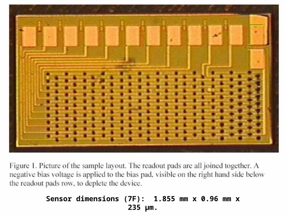
Sensor dimensions (7F): 1.855 mm x 0.96 mm x 235 µm.


Preliminary calculation of the α parameter for a volume of 0.418 mm2 is 3.8 x10⁻¹⁷. This assumes the leakage current to be generated by the device full physical volume.
0.64 3.7 6.0 8.6 x e15

Oscilloscope trace of an alpha particle with the corresponding histogram (generated automatically by the oscilloscope), measured at –15C using the sample 7F with 140V bias. The vertical scale is 500mV/div.
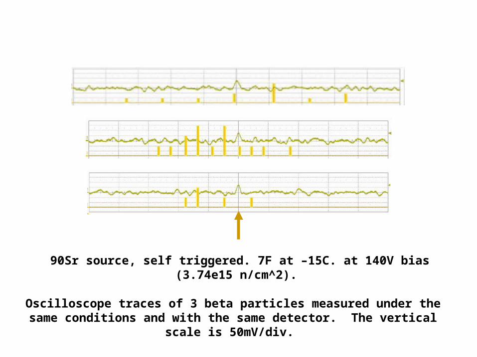
90Sr source, self triggered. 7F at –15C. at 140V bias (3.74e15 n/cm^2).
Oscilloscope traces of 3 beta particles measured under the same conditions and with the same detector. The vertical scale is 50mV/div.

Outline: Pixels – replacement / upgrade
• 1. what is needed• 2. basic 3D properties• 3. how they help• 4. results – first irradiation• 5. results – speed, active edges• 6. results – ATLAS front end chip• 7. results – second irradiation• 8. improved yield: planar/3D active edges• 9. improving yield: current run• 10. ongoing measurements
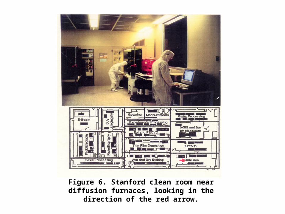
Figure 6. Stanford clean room near diffusion furnaces, looking in the direction of the red arrow.

Pictures of clean rooms like the one preceding are familiar, but many other things are needed for high yield, for example: specific, careful checking of the results of each of the 37 main steps and of the many sub-steps, cleanliness not just of the room and air, but of everything used – tools, chemicals, cassettes, etc.
The deep etching may leave an uneven surface that makes it difficult to spin on a uniform layer of photoresist for a following lithography step. If this step is a deep etch, a thick resist is needed. They seem to have a higher level of particulates and clumps of resist.
Active edge fabrication requires support wafers, which must be oxide-bonded to the sensor wafer under extremely clean conditions.

The following specific steps were added to the fabrication procedure for the two-order-of-magnitude larger, 9 cm2 planar / 3D active edge Totem sensors:
1. The wafers were carefully inspected after every litho step. If defects were seen, the resist was removed, new resist was applied, and the wafers were re-spun and re-exposed.
2. Defects in the thick resist used for the trench etch were covered with polyimide.
3. The surface planarity in the region of the dips at the centers of the poly-filled electrodes was improved by etching the poly off the top surface, and then repeating the fill and etch procedure.
4. The plasma dice lane was widened from 50 microns to 120 microns. The more open trench prevented the formation of silicon chips along the trench edges. This seems to have eliminated this defect class, which caused a 25% loss for the first batch.
5. Evaporated aluminum instead of sputtered gold was used for the backside contact.

In the first Totem fabrication run of full-size sensors, only 1 of 28 sensors had 99% or more good strips. After the 5 yield enhancement steps were added,13 of 20 sensors from the next run had at least 99% good strips:
Now we must produce similar results for full 3D sensors.
Outline: Pixels – replacement / upgrade
• 1. what is needed• 2. basic 3D properties• 3. how they help• 4. results – first irradiation• 5. results – speed, active edges• 6. results – ATLAS front end chip• 7. results – second irradiation• 8. improved yield: planar/3D active edges• 9. improving yield: current run• 10. ongoing measurements
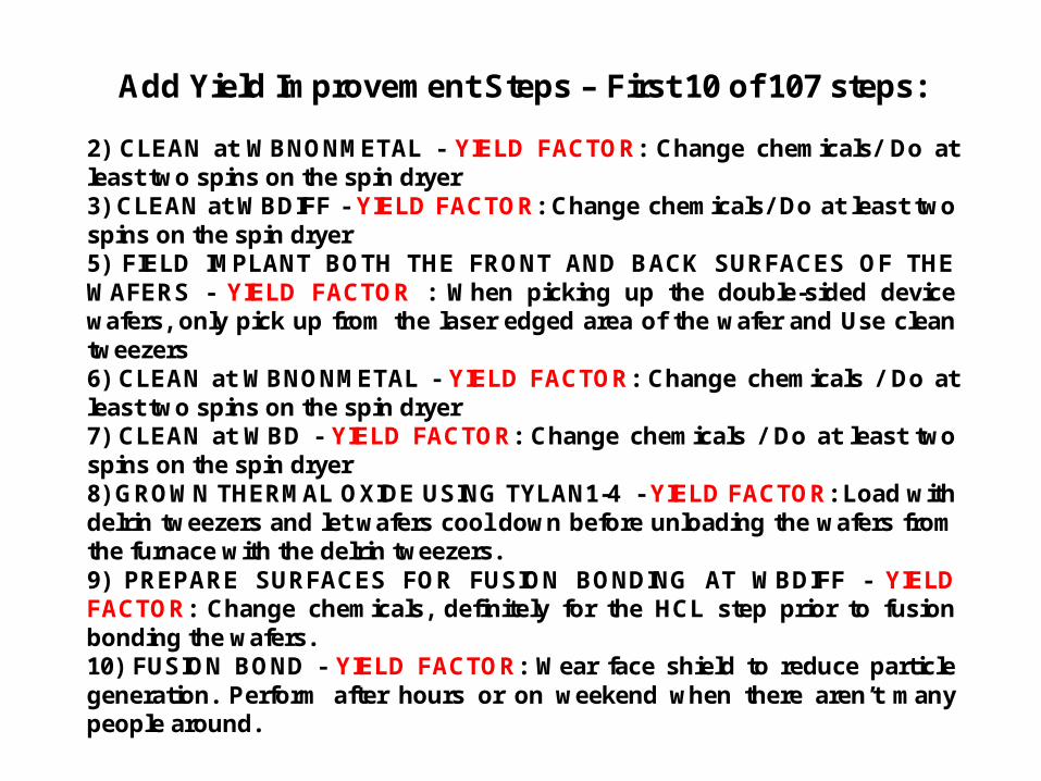
Add Yield Improvement Steps – First 10 of 107 steps:
2) CLEAN at WBNONMETAL - YIELD FACTOR: Change chemicals/ Do at least two spins on the spin dryer3) CLEAN at WBDIFF - YIELD FACTOR: Change chemicals/ Do at least two spins on the spin dryer5) FIELD IMPLANT BOTH THE FRONT AND BACK SURFACES OF THE WAFERS - YIELD FACTOR : When picking up the double-sided device wafers, only pick up from the laser edged area of the wafer and Use clean tweezers6) CLEAN at WBNONMETAL - YIELD FACTOR: Change chemicals / Do at least two spins on the spin dryer7) CLEAN at WBD - YIELD FACTOR: Change chemicals / Do at least two spins on the spin dryer8) GROWN THERMAL OXIDE USING TYLAN1-4 - YIELD FACTOR: Load with delrin tweezers and let wafers cool down before unloading the wafers from the furnace with the delrin tweezers.9) PREPARE SURFACES FOR FUSION BONDING AT WBDIFF - YIELD FACTOR: Change chemicals, definitely for the HCL step prior to fusion bonding the wafers.10) FUSION BOND - YIELD FACTOR: Wear face shield to reduce particle generation. Perform after hours or on weekend when there aren’t many people around.

Outline: Pixels – replacement / upgrade
• 1. what is needed• 2. basic 3D properties• 3. how they help• 4. results – first irradiation• 5. results – speed, active edges• 6. results – ATLAS front end chip• 7. results – second irradiation• 8. improved yield: planar/3D active edges• 9. improving yield: current run• 10. ongoing measurements

1. Univ. of New Mexico (following talk)
2. Praha: Cinzia Da Via will travel there next week to continue her measurements on the irradiated ATLAS pixel spacing sensors:
a. add a trigger for 90-Sr betas after the sensors
b. measurements with flood beam, pulsed, infrared laser illumination
3. infrared laser flood beam measurements: (note: ir diode also ok)
a. pulse time long compared to collection times, short compared to trapping times and to R (probe) x C (probe + electrode)
b. pulse generator triggers digital scope
c. sweep is long enough to get:
noise and baseline (for subtraction) from trace ahead of trigger,trapped-charge release signals after trigger
d. on-time average V-signal vs. V-bias gives depleted volume, collection efficiency
e. RC fall time gives C (electrode); tail gives charge capture information
f. systematic checks will be needed (results should be independent of laser intensity, exact aim of beam, etc.)
Related Documents