metals Review 3D Printing of Highly Pure Copper Thang Q. Tran 1, *, Amutha Chinnappan 1 , Jeremy Kong Yoong Lee 1 , Nguyen Huu Loc 2 , Long T. Tran 2 , Gengjie Wang 3 , Vishnu Vijay Kumar 1 , W. A. D. M. Jayathilaka 1 , Dongxiao Ji 1 , Mrityunjay Doddamani 4 and Seeram Ramakrishna 1, * 1 Department of Mechanical Engineering, National University of Singapore, 9 Engineering Drive 1, EA-07-05, Singapore 117575, Singapore 2 Faculty of Mechanical Engineering, Ho Chi Minh City University of Technology, VNUHCM, 268 Ly Thuong Kiet, District 10, Ho Chi Minh City 740400, Vietnam 3 Institute of Materials Engineering, National Laboratory of Solid State Microstructures, College of Engineering and Applied Sciences, Nanjing University, Nanjing 210093, China 4 Lightweight Materials Laboratory, Department of Mechanical Engineering, National Institute of Technology Karnataka, Surathkal 575025, India * Correspondence: [email protected] (T.Q.T.); [email protected] (S.R.) Received: 14 June 2019; Accepted: 2 July 2019; Published: 5 July 2019 Abstract: Copper has been widely used in many applications due to its outstanding properties such as malleability, high corrosion resistance, and excellent electrical and thermal conductivities. While 3D printing can offer many advantages from layer-by-layer fabrication, the 3D printing of highly pure copper is still challenging due to the thermal issues caused by copper’s high conductivity. This paper presents a comprehensive review of recent work on 3D printing technology of highly pure copper over the past few years. The advantages and current issues of 3D printing methods are compared while different properties of copper parts printed by these methods are summarized. Finally, we provide several potential applications of the 3D printed copper parts and an overview of current developments that could lead to new improvements in this advanced manufacturing field. Keywords: copper; additive manufacturing; selective laser melting; electron beam melting; binder jetting; ultrasonic additive manufacturing 1. Introduction During the last decades, 3D printing of metallic parts directly from 3D computer-aided design (CAD) models has drawn significant attention from both academia and industry [1–6]. One of the important advantages of 3D printing is the higher design freedom compared to conventional fabrication technologies [7–10]. In fact, complex 3D parts such as components with many internal structures or cellular parts can be fabricated by 3D printing without considering specific design rules. Moreover, the topological optimization of 3D CAD models with no additional cost in 3D printing provides many advantages such as complex shapes, short lead times, weight saving, and multifunctional integration [11]. Nowadays, many high-performance metallic alloys and pure metals can be processed successfully with achievable properties comparable to those fabricated by conventional methods such as forming or casting [1–4]. Additionally, parts with epitaxial growth and fine microstructures can be fabricated by process-inherent rapid and direct solidification in 3D printing. This offers a great potential in new design possibilities to achieve locally-desired material properties. Besides, the application of high cooling rates during 3D printing processes provides new possibilities in alloy and metal design [1–4]. 3D printing of highly pure copper with superior electrical and thermal properties has been studied extensively due to its broad potential in many applications including electronic devices [1,12–20], thermal management systems [4,12], and the aerospace industry [4,12,21–25]. Compared to conventional Metals 2019, 9, 756; doi:10.3390/met9070756 www.mdpi.com/journal/metals

Welcome message from author
This document is posted to help you gain knowledge. Please leave a comment to let me know what you think about it! Share it to your friends and learn new things together.
Transcript

metals
Review
3D Printing of Highly Pure Copper
Thang Q Tran 1 Amutha Chinnappan 1 Jeremy Kong Yoong Lee 1 Nguyen Huu Loc 2Long T Tran 2 Gengjie Wang 3 Vishnu Vijay Kumar 1 W A D M Jayathilaka 1 Dongxiao Ji 1Mrityunjay Doddamani 4 and Seeram Ramakrishna 1
1 Department of Mechanical Engineering National University of Singapore 9 Engineering Drive 1EA-07-05 Singapore 117575 Singapore
2 Faculty of Mechanical Engineering Ho Chi Minh City University of Technology VNUHCM268 Ly Thuong Kiet District 10 Ho Chi Minh City 740400 Vietnam
3 Institute of Materials Engineering National Laboratory of Solid State MicrostructuresCollege of Engineering and Applied Sciences Nanjing University Nanjing 210093 China
4 Lightweight Materials Laboratory Department of Mechanical Engineering National Institute of TechnologyKarnataka Surathkal 575025 India
Correspondence tranquyetthangunusedu (TQT) seeramnusedusg (SR)
Received 14 June 2019 Accepted 2 July 2019 Published 5 July 2019
Abstract Copper has been widely used in many applications due to its outstanding properties suchas malleability high corrosion resistance and excellent electrical and thermal conductivities While3D printing can offer many advantages from layer-by-layer fabrication the 3D printing of highlypure copper is still challenging due to the thermal issues caused by copperrsquos high conductivityThis paper presents a comprehensive review of recent work on 3D printing technology of highlypure copper over the past few years The advantages and current issues of 3D printing methodsare compared while different properties of copper parts printed by these methods are summarizedFinally we provide several potential applications of the 3D printed copper parts and an overview ofcurrent developments that could lead to new improvements in this advanced manufacturing field
Keywords copper additive manufacturing selective laser melting electron beam melting binderjetting ultrasonic additive manufacturing
1 Introduction
During the last decades 3D printing of metallic parts directly from 3D computer-aided design(CAD) models has drawn significant attention from both academia and industry [1ndash6] One of theimportant advantages of 3D printing is the higher design freedom compared to conventional fabricationtechnologies [7ndash10] In fact complex 3D parts such as components with many internal structures orcellular parts can be fabricated by 3D printing without considering specific design rules Moreoverthe topological optimization of 3D CAD models with no additional cost in 3D printing provides manyadvantages such as complex shapes short lead times weight saving and multifunctional integration [11]Nowadays many high-performance metallic alloys and pure metals can be processed successfullywith achievable properties comparable to those fabricated by conventional methods such as forming orcasting [1ndash4] Additionally parts with epitaxial growth and fine microstructures can be fabricated byprocess-inherent rapid and direct solidification in 3D printing This offers a great potential in new designpossibilities to achieve locally-desired material properties Besides the application of high cooling ratesduring 3D printing processes provides new possibilities in alloy and metal design [1ndash4]
3D printing of highly pure copper with superior electrical and thermal properties has beenstudied extensively due to its broad potential in many applications including electronic devices [112ndash20]thermal management systems [412] and the aerospace industry [41221ndash25] Compared to conventional
Metals 2019 9 756 doi103390met9070756 wwwmdpicomjournalmetals
Metals 2019 9 756 2 of 24
fabrication methods such as metal casting welding and machining 3D printing can fabricate moreoptimized and complex 3D copper parts without using additional tools [26ndash34] Post-processing methodssuch as abrasive polishing [35] and hot isostatic pressing (HIP) [36ndash39] could enhance physical propertiesof the printed copper parts further However 3D printing of pure copper has several significantprocessing challenges that need to be addressed Due to copperrsquos high thermal conductivity the meltarea experiences rapid heat dissipation and high local thermal gradients resulting in delaminationlayer curling and part failure [4041] Furthermore the post-build powder removal and recovery ofthe printed parts might be impeded by the high ductility of copper while the tendency of powderagglomeration could lower overall flowability and hinder powder deposition Additionally specialhandling and storage of copper are required for 3D printing processes due to the high sensitivity ofcopper to oxidation [40ndash42]
Although many papers have been published on 3D printing of highly pure copper [1221264043]no comprehensive review has been reported Recent rapid growth in research on the 3D printing ofpure copper has motivated this review In Section 2 we present the main 3D printing methods forpure copper over the past few years The advantages and challenges of each 3D printing methodare discussed in Section 3 In Section 4 the potential applications of 3D printed copper parts aresummarized and a brief conclusion is presented in Section 5
2 3D Printing Methods of Highly Pure Copper
21 Selective Laser Melting
Selective laser melting (SLM) is a widely used powder bed-based process to fabricate metallicparts [44ndash48] The building process starts with spreading metal powder in thin layers across a workarea (Figure 1a) [13] The metal powder is usually fed by a hopper while a recoater blade is used toensure uniform powder distribution (Figure 1b Step I) Then a galvanometer scanner is employed todirect a high energy density laser beam across the deposited layer of the metal powder (Figure 1bStep II) According to the CAD data of the fabricated part only metal powder in the selected areas isexposed to the laser beam and melted along the part contour and filling in the XY plane (Figure 1a B-B)The build platform is lowered (Figure 1b Step III) subsequently and a new powder layer is depositedfor the next laser scanning step These three steps are repeated until the required part is fully built
Metals 2019 9 x FOR PEER REVIEW 2 of 24
3D printing of highly pure copper with superior electrical and thermal properties has been studied extensively due to its broad potential in many applications including electronic devices [112ndash20] thermal management systems [412] and the aerospace industry [41221ndash25] Compared to conventional fabrication methods such as metal casting welding and machining 3D printing can fabricate more optimized and complex 3D copper parts without using additional tools [26ndash34] Post-processing methods such as abrasive polishing [35] and hot isostatic pressing (HIP) [36ndash39] could enhance physical properties of the printed copper parts further However 3D printing of pure copper has several significant processing challenges that need to be addressed Due to copperrsquos high thermal conductivity the melt area experiences rapid heat dissipation and high local thermal gradients resulting in delamination layer curling and part failure [4041] Furthermore the post-build powder removal and recovery of the printed parts might be impeded by the high ductility of copper while the tendency of powder agglomeration could lower overall flowability and hinder powder deposition Additionally special handling and storage of copper are required for 3D printing processes due to the high sensitivity of copper to oxidation [40ndash42]
Although many papers have been published on 3D printing of highly pure copper [1221264043] no comprehensive review has been reported Recent rapid growth in research on the 3D printing of pure copper has motivated this review In Section 2 we present the main 3D printing methods for pure copper over the past few years The advantages and challenges of each 3D printing method are discussed in Section 3 In Section 4 the potential applications of 3D printed copper parts are summarized and a brief conclusion is presented in Section 5
2 3D Printing Methods of Highly Pure Copper
21 Selective Laser Melting
Selective laser melting (SLM) is a widely used powder bed-based process to fabricate metallic parts [44ndash48] The building process starts with spreading metal powder in thin layers across a work area (Figure 1a) [13] The metal powder is usually fed by a hopper while a recoater blade is used to ensure uniform powder distribution (Figure 1b Step I) Then a galvanometer scanner is employed to direct a high energy density laser beam across the deposited layer of the metal powder (Figure 1b Step II) According to the CAD data of the fabricated part only metal powder in the selected areas is exposed to the laser beam and melted along the part contour and filling in the XY plane (Figure 1a B-B) The build platform is lowered (Figure 1b Step III) subsequently and a new powder layer is deposited for the next laser scanning step These three steps are repeated until the required part is fully built
Figure 1 (a) Schematics of a selective laser melting (SLM) machine and (b) the three-step process repeated during the build [1] with permission from Elsevier 2019
Figure 1 (a) Schematics of a selective laser melting (SLM) machine and (b) the three-step processrepeated during the build [1] with permission from Elsevier 2019
The build plate is usually connected to support structures which are necessary for the partrsquosfixation in the powder bed and heat dissipation (Figure 1a Detail A) The distortion of the printed partscan be avoided by pre-heating the build plate to lower thermal gradients and reduce residual stressesduring the SLM process Inert gas such as nitrogen or argon is continuously supplied to the buildingchamber to provide an inert atmosphere for protecting the metal powder and the heated metal parts
Metals 2019 9 756 3 of 24
from oxidation Once the printing process is completed the substrate plate can be removed from theprinted part Important process parameters such as layer thickness hatch spacing laser power andscanning speed need to be optimized to fabricate high quality printed parts [13]
211 Indirect Selective Laser Melting
Badrinarayan et al [49] first reported the indirect manufacturing of pure copper parts using theSLM method A powder mixture of copper and poly(methyl methacrylate) (PMMA) was used as afeedstock for the printing process Since PMMA acted as an intermediate binder it was melted duringthe laser scanning process to bind the copper powders and form copper green parts The green partswere debinded under reducing conditions afterwards and the resulting copper parts were sintered forseveral hours However the mixing ratio of PMMA in the fabrication process was too high (8 wt)leading to the low green density (under 27) [4950] Consequently the sintered copper parts had adensity much lower than the theoretical density (about 77ndash88) with the introduction of significantporosity To address the issue polymer-coated granules of small copper particles and bimodal mixedpowders could be used to improve the powder packing density Another drawback of the indirectSLM was that the impurities from the debinding process could be introduced to the final copper partsand might lower their properties [4950]
212 Direct Selective Laser Melting
Most commercial SLM systems use continuous wave and long-pulse lasers working in the nearinfrared radiation (IR) with a wavelength of about 1 microm [5152] Although SLM has been demonstratedfor many materials ranging from metals to polymers and ceramics [53ndash58] the processing of materialswith high thermal conductivities and high melting points such as pure copper is still challenging [5960]In addition to the rapid heat dissipation problems reflectivity of copper to conventional laser lightnear IR is very high [61ndash63] resulting in low deposition of laser energy in the materials for themelting process [51] Therefore to achieve high laser energy density for fabricating dense copperparts greater laser output power and lower scanning speed layer thickness and hatch spacing arerequired [525964]
Generally the minimal laser power for a successful SLM of pure copper is approximately 300W although some studies have reported the fabrication of copper parts at lower laser powers [6566]Lykov et al [65] studied the SLM process of pure copper powder using a system equipped with a200 W CO2 laser source The process used a scanning speed ranging between 100 and 150 mmswhereas the layer thickness and hatch spacing were fixed at 50 microm and 012 mm respectively Althoughthe absorptance of pure copper powder for CO2 laser was very low (only 026) the copper powdercould be selectively melted since the laser beam diameter was adjusted to as small as 35 microm to obtainsufficient power density for the melting process Consequently the printed copper parts had densestructures with good surface finish quality and no dimensional distortions were observed Specificallythe relative density of the printed parts could be as high as 881 while their tensile strength couldreach 149 MPa [65]
In another approach Kaden et al [52] reported a successful SLM process of pure copper byusing ultrashort laser pulses with 500 fs pulse duration at a center wavelength of 1030 nm At a20 MHz repetition rate the lasers could provide extremely high pulse energy (1ndash15 microJ) and line energy(100 Jm) which were sufficient for copper melting The powder layer thickness and laser spot sizewere controlled at 30 microm and of 35 microm respectively to fabricate both bulky and thin-walled copperstructures with thicknesses below 100 microm (Figure 2) The scanning electron microscope (SEM) imagesin Figure 2b suggested that the printed parts had porous structures with melting beads formed duringthe powder melting This might stem from the large powder size (35 microm) compared to the laser spotdiameter (35 microm) employed in the process Therefore the use of copper powder with small grain sizeswas recommended to reduce porous structures of the printed copper parts and improve their relativedensity [52]
Metals 2019 9 756 4 of 24
Metals 2019 9 x FOR PEER REVIEW 4 of 24
laser spot diameter (35 microm) employed in the process Therefore the use of copper powder with small grain sizes was recommended to reduce porous structures of the printed copper parts and improve their relative density [52]
Figure 2 (a) Sample of different thin wall structures and (b) SEM image of a single wall [52] with permission from Springer Nature 2019
By using a laser source with much higher power Ikeshoji et al [64] could fabricate 3D copper parts with a relative density of up to 966 by SLM In the fabrication process the laser power was set at 800 W and the used hatch pitch was in a range of 0025ndash012 mm Additionally the scanning speed and powder bed thickness were fixed at 300 mms and 005 mm respectively As can be seen in Figure 3a the surfaces of all the printed cubes had rough texture and ballshaped asperities with no severe oxidation observed These ball-shaped asperities might stem from the nonmolten residual powder particles while large asperities might be formed by splatter Also the surface texture suggested the presence of voids within the copper structures [64]
Figure 3 (a) Cubes built by SLM of 999 pure copper powder and (b) relative density of SLM-built cubes of pure copper [64] with permission from Springer Nature 2019
Due to the large asperities smooth powder bed surfaces might not be achieved during the squeezing process Internal voids could be formed at the shadow of the laser irradiation under the ball-like asperities and therefore lowered the relative density of the printed parts As shown in Figure 3b the relative density of the printed parts decreased at narrower hatch pitches although the asperities could be exposed to the laser beam several times and melted down to fill the voids during the laser scanning process Besides transient heat transfer including melting and solidification was
Figure 2 (a) Sample of different thin wall structures and (b) SEM image of a single wall [52] withpermission from Springer Nature 2019
By using a laser source with much higher power Ikeshoji et al [64] could fabricate 3D copperparts with a relative density of up to 966 by SLM In the fabrication process the laser power wasset at 800 W and the used hatch pitch was in a range of 0025ndash012 mm Additionally the scanningspeed and powder bed thickness were fixed at 300 mms and 005 mm respectively As can be seenin Figure 3a the surfaces of all the printed cubes had rough texture and ballshaped asperities withno severe oxidation observed These ball-shaped asperities might stem from the nonmolten residualpowder particles while large asperities might be formed by splatter Also the surface texture suggestedthe presence of voids within the copper structures [64]
Metals 2019 9 x FOR PEER REVIEW 4 of 24
laser spot diameter (35 microm) employed in the process Therefore the use of copper powder with small grain sizes was recommended to reduce porous structures of the printed copper parts and improve their relative density [52]
Figure 2 (a) Sample of different thin wall structures and (b) SEM image of a single wall [52] with permission from Springer Nature 2019
By using a laser source with much higher power Ikeshoji et al [64] could fabricate 3D copper parts with a relative density of up to 966 by SLM In the fabrication process the laser power was set at 800 W and the used hatch pitch was in a range of 0025ndash012 mm Additionally the scanning speed and powder bed thickness were fixed at 300 mms and 005 mm respectively As can be seen in Figure 3a the surfaces of all the printed cubes had rough texture and ballshaped asperities with no severe oxidation observed These ball-shaped asperities might stem from the nonmolten residual powder particles while large asperities might be formed by splatter Also the surface texture suggested the presence of voids within the copper structures [64]
Figure 3 (a) Cubes built by SLM of 999 pure copper powder and (b) relative density of SLM-built cubes of pure copper [64] with permission from Springer Nature 2019
Due to the large asperities smooth powder bed surfaces might not be achieved during the squeezing process Internal voids could be formed at the shadow of the laser irradiation under the ball-like asperities and therefore lowered the relative density of the printed parts As shown in Figure 3b the relative density of the printed parts decreased at narrower hatch pitches although the asperities could be exposed to the laser beam several times and melted down to fill the voids during the laser scanning process Besides transient heat transfer including melting and solidification was
Figure 3 (a) Cubes built by SLM of 999 pure copper powder and (b) relative density of SLM-builtcubes of pure copper [64] with permission from Springer Nature 2019
Due to the large asperities smooth powder bed surfaces might not be achieved during thesqueezing process Internal voids could be formed at the shadow of the laser irradiation under theball-like asperities and therefore lowered the relative density of the printed parts As shown inFigure 3b the relative density of the printed parts decreased at narrower hatch pitches although theasperities could be exposed to the laser beam several times and melted down to fill the voids duringthe laser scanning process Besides transient heat transfer including melting and solidification wasanalyzed by the finite element method (FEM) to study the effects of hatch pitches on the SLM process ofpure copper The various predicted dimensions of the melt pool with time indicated a slight overlap for
Metals 2019 9 756 5 of 24
wider hatch pitches and instability for narrower hatch pitches This result suggested that the relativedensity of the printed copper parts was strongly related to the hatch pitch [64]
Later a feasibility window of the SLM process of pure Cu powder was investigated byColopi et al [59] using a 1kW laser source A total of 70 experimental conditions were conducted byvarying the laser power layer thickness and scan speed in ranges of 200ndash1000 W 50ndash100 microm and1000ndash4000 mms respectively The process outcome was classified into three categories not fused(insufficient solidification) delamination (insufficient interlayer bonding) and acceptable (no evidentdefect) As shown in Figure 4a the process using a layer thickness of 50 microm had the widest stabilityregion which might stem from its higher process resolution
Metals 2019 9 x FOR PEER REVIEW 5 of 24
analyzed by the finite element method (FEM) to study the effects of hatch pitches on the SLM process of pure copper The various predicted dimensions of the melt pool with time indicated a slight overlap for wider hatch pitches and instability for narrower hatch pitches This result suggested that the relative density of the printed copper parts was strongly related to the hatch pitch [64]
Later a feasibility window of the SLM process of pure Cu powder was investigated by Colopi et al [59] using a 1kW laser source A total of 70 experimental conditions were conducted by varying the laser power layer thickness and scan speed in ranges of 200ndash1000 W 50ndash100 microm and 1000ndash4000 mms respectively The process outcome was classified into three categories not fused (insufficient solidification) delamination (insufficient interlayer bonding) and acceptable (no evident defect) As shown in Figure 4a the process using a layer thickness of 50 microm had the widest stability region which might stem from its higher process resolution
Figure 4 (a) Qualitative categorization of process outcome Feasibility region for SLM of pure Cu indicated by dashed blue line (b) cross-section of a cubic specimen representative of an ldquoacceptablerdquo processing conditions and (c) final demonstrator of pure Cu powder processability [59] with permission from Elsevier 2019
The ldquodelaminationrdquo defect occurred in both layer thicknesses suggesting the crucial role of inter-layer bonding on obtaining a stable powder bed densification The occurrence of this defect at low laser power indicated the instability of the process melt pool (Figure 4a) Since the previously deposited copper layer had high thermal conductivity thermal cooling could be elevated while melt pool stability might be hindered Besides the formation of the inter-layer defect might lead to thermally insulating gases in between the layers and hence limit the penetration of the melt pool to the previous interlayer defect Consequently the delamination issue might be further worsened due to the formation of thermally-induced stresses resulting in more defect formation and part deformations [59]
As shown in Figure 4bc the relative density of the printed copper parts yielded up to 978 of the separate measurement between the core volume of sections and the border The porosity in the border regions was always higher which might be attributed to the temperature differences between the border and the central region Due to thermal accumulation most internal regions could reach higher temperatures compared to the border Furthermore the border was usually in contact with cooler powder in the powder bed during the scanning process Since copper has very high thermal conductivity strong thermal dissipation could be achieved in the border areas resulting in their partial melting and higher porosity The process parameters optimized the feasibility window which could be used to produce complex 3D copper parts as shown in Figure 4c [59]
Figure 4 (a) Qualitative categorization of process outcome Feasibility region for SLM of pure Cuindicated by dashed blue line (b) cross-section of a cubic specimen representative of an ldquoacceptablerdquoprocessing conditions and (c) final demonstrator of pure Cu powder processability [59] with permissionfrom Elsevier 2019
The ldquodelaminationrdquo defect occurred in both layer thicknesses suggesting the crucial role ofinter-layer bonding on obtaining a stable powder bed densification The occurrence of this defect at lowlaser power indicated the instability of the process melt pool (Figure 4a) Since the previously depositedcopper layer had high thermal conductivity thermal cooling could be elevated while melt pool stabilitymight be hindered Besides the formation of the inter-layer defect might lead to thermally insulatinggases in between the layers and hence limit the penetration of the melt pool to the previous interlayerdefect Consequently the delamination issue might be further worsened due to the formation ofthermally-induced stresses resulting in more defect formation and part deformations [59]
As shown in Figure 4bc the relative density of the printed copper parts yielded up to 978 ofthe separate measurement between the core volume of sections and the border The porosity in theborder regions was always higher which might be attributed to the temperature differences betweenthe border and the central region Due to thermal accumulation most internal regions could reachhigher temperatures compared to the border Furthermore the border was usually in contact withcooler powder in the powder bed during the scanning process Since copper has very high thermalconductivity strong thermal dissipation could be achieved in the border areas resulting in their partialmelting and higher porosity The process parameters optimized the feasibility window which could beused to produce complex 3D copper parts as shown in Figure 4c [59]
Metals 2019 9 756 6 of 24
Jadhav et al [51] studied the influences of different laser scan parameters on the texturaldevelopment of SLM-printed copper parts The fabrication process used a 1 kW laser source with abeam diameter of 40 microm and a layer thickness of 30 microm At optimum processing conditions printedparts with a relative density of more than 98 electrical conductivity of 88 IACS (InternationalAnnealed Copper Standard definition of 58 MSm as 100 IACS for electrical conductivity) andthermal conductivity of up to 336 WmK could be produced (Figure 5ab)
Metals 2019 9 x FOR PEER REVIEW 6 of 24
Jadhav et al [51] studied the influences of different laser scan parameters on the textural development of SLM-printed copper parts The fabrication process used a 1 kW laser source with a beam diameter of 40 microm and a layer thickness of 30 microm At optimum processing conditions printed parts with a relative density of more than 98 electrical conductivity of 88 IACS (International Annealed Copper Standard definition of 58 MSm as 100 IACS for electrical conductivity) and thermal conductivity of up to 336 WmK could be produced (Figure 5ab)
Figure 5 (a) Fabricated cube shaped parts along with the corresponding SLM process parametersmdashP in Watt h in mm and v in mms (b) relative density () of parts versus applied energy densities (Jmm3) Parts with a stable geometry are marked with a circle (c) SEM image of sample top surfaces processed with different SLM scan parameters The laser scan direction is indicated by the white dashed arrows (d) Damages to the optical mirror in the SLM machine after 12 h exposure to laser back reflection [51] with permission from Elsevier 2019
The analysis of the crystallographic texture of the SLM copper parts suggested that the crystal orientation of the YZ and middle (XY-MID) plane was relatively random This result could be attributed to the alteration in the heat gradient directions and subsequent re-melting which were formed by applying a 90deg scan rotation strategy in between the subsequent layers However the top surface (XY-TOP) had strong crystallographic texture owing to the solidification morphology controlled by the temperature gradients within the melt pools Due to the extremely high laser energy density and laser power used in the process damages of the optical coating could be formed on the laser mirror as shown in Figure 5d [51]
22 Electron Beam Melting
Similar to SLM electron beam melting (EBM) is also a common powder bed-based process used to fabricate highly-dense metallic parts [6768] In the EBM process metal powder from a hopper is supplied and spread uniformly on a build plate by a rake (Figure 6) [169] The powder layer thickness is usually in the range of 50ndash200 microm According to the CAD data the powder is melted selectively
Figure 5 (a) Fabricated cube shaped parts along with the corresponding SLM process parametersmdashP inWatt h in mm and v in mms (b) relative density () of parts versus applied energy densities (Jmm3)Parts with a stable geometry are marked with a circle (c) SEM image of sample top surfaces processedwith different SLM scan parameters The laser scan direction is indicated by the white dashed arrows(d) Damages to the optical mirror in the SLM machine after 12 h exposure to laser back reflection [51]with permission from Elsevier 2019
The analysis of the crystallographic texture of the SLM copper parts suggested that the crystalorientation of the YZ and middle (XY-MID) plane was relatively random This result could be attributedto the alteration in the heat gradient directions and subsequent re-melting which were formed byapplying a 90 scan rotation strategy in between the subsequent layers However the top surface(XY-TOP) had strong crystallographic texture owing to the solidification morphology controlled bythe temperature gradients within the melt pools Due to the extremely high laser energy density andlaser power used in the process damages of the optical coating could be formed on the laser mirroras shown in Figure 5d [51]
22 Electron Beam Melting
Similar to SLM electron beam melting (EBM) is also a common powder bed-based process usedto fabricate highly-dense metallic parts [6768] In the EBM process metal powder from a hopper issupplied and spread uniformly on a build plate by a rake (Figure 6) [169] The powder layer thickness
Metals 2019 9 756 7 of 24
is usually in the range of 50ndash200 microm According to the CAD data the powder is melted selectivelyusing an electron beam as a heat source The electron beam is produced by an electron gun andaccelerated with a high acceleration voltage Then electromagnetic lenses are used to focus the beamand a magnetic scan coil is employed to direct it to selected areas of the metal layers in the XY planeImportant EBM process parameters such as electron beam power scan speed and focus of the electronbeam usually depend on the speed function beam current and focus offset respectively [70]
At first a defocused beam pre-heats the powder bed by scanning the powder bed surface severaltimes Then a high beam current and proper scan speed are employed to heat and sinter the powderSimilar to the SLM process the build plate in EBM is then lowered and metal powder is fed and spreaduniformly across the work area The process of powder deposition powder pre-heating electronbeam scanning and build plate lowering is repeated until the part printing is completed The EBMprocess operates under a vacuum and helium is fed to the work area to prevent the metal powder fromelectrical charging while improving the heat conduction and cooling of the melt [171]
Metals 2019 9 x FOR PEER REVIEW 7 of 24
using an electron beam as a heat source The electron beam is produced by an electron gun and accelerated with a high acceleration voltage Then electromagnetic lenses are used to focus the beam and a magnetic scan coil is employed to direct it to selected areas of the metal layers in the XY plane Important EBM process parameters such as electron beam power scan speed and focus of the electron beam usually depend on the speed function beam current and focus offset respectively [70]
At first a defocused beam pre-heats the powder bed by scanning the powder bed surface several times Then a high beam current and proper scan speed are employed to heat and sinter the powder Similar to the SLM process the build plate in EBM is then lowered and metal powder is fed and spread uniformly across the work area The process of powder deposition powder pre-heating electron beam scanning and build plate lowering is repeated until the part printing is completed The EBM process operates under a vacuum and helium is fed to the work area to prevent the metal powder from electrical charging while improving the heat conduction and cooling of the melt [171]
Figure 6 Schematics of electron beam melting (EBM) 1 electron gun 2 lens system 3 deflection lens 4 powder cassettes with feedstock 5 rake 6 building component 7 build table [69] with permission from Elsevier 2019
Since electrons have different absorption and reflection mechanisms compared to photons the EBM method is not affected by the optical reflectivity of materials and most of the energy in EBM is deposited within the materials [144072] Therefore this method has a high potential for the processing of pure copper [7374] Furthermore the sintering step of copper during the EBM process can be extremely short due to its high electrical conductivity In fact the copper powder might not be removed if preheating is too high or too long because it has high sintering activity [1440] Yang et al [28] reported the fabrication of pure copper with orthotropic re-entrant auxetic structures using EBM Because of the high thermal conductivity of copper the dissipation of thermal energy during the melting process was severe resulting in large variations in the dimensions and mechanical performance of the printed copper parts Therefore more process optimization was required to improve the surface quality and accuracy of the printed parts
Since copper is quite sensitive to oxidation its storage and handling should be considered properly [75] Ramirez et al [76] investigated the effects of Cu2O on the microstructure of the EBM-printed copper components with the use of a relatively impure Cu precursor powder (985) The study results showed the formation of precipitationndashdislocation architectures because of directional
Figure 6 Schematics of electron beam melting (EBM) 1 electron gun 2 lens system 3 deflection lens4 powder cassettes with feedstock 5 rake 6 building component 7 build table [69] with permissionfrom Elsevier 2019
Since electrons have different absorption and reflection mechanisms compared to photons the EBMmethod is not affected by the optical reflectivity of materials and most of the energy in EBM is depositedwithin the materials [144072] Therefore this method has a high potential for the processing of purecopper [7374] Furthermore the sintering step of copper during the EBM process can be extremelyshort due to its high electrical conductivity In fact the copper powder might not be removed ifpreheating is too high or too long because it has high sintering activity [1440] Yang et al [28] reportedthe fabrication of pure copper with orthotropic re-entrant auxetic structures using EBM Because of thehigh thermal conductivity of copper the dissipation of thermal energy during the melting processwas severe resulting in large variations in the dimensions and mechanical performance of the printedcopper parts Therefore more process optimization was required to improve the surface quality andaccuracy of the printed parts
Metals 2019 9 756 8 of 24
Since copper is quite sensitive to oxidation its storage and handling should be consideredproperly [75] Ramirez et al [76] investigated the effects of Cu2O on the microstructure of theEBM-printed copper components with the use of a relatively impure Cu precursor powder (985)The study results showed the formation of precipitationndashdislocation architectures because of directionalsolidification during EBM (Figure 7a) Interestingly these precipitationndashdislocation architecturesimproved the hardness of the parts from HV 57 for a base-plate to HV 88 for EBM-printed productsSimilar phenomenon was also observed in their later study of the open-cellular copper structures(Figure 7b) produced by EBM of higher purity copper powder (998) [26]
Metals 2019 9 x FOR PEER REVIEW 8 of 24
solidification during EBM (Figure 7a) Interestingly these precipitationndashdislocation architectures improved the hardness of the parts from HV 57 for a base-plate to HV 88 for EBM-printed products Similar phenomenon was also observed in their later study of the open-cellular copper structures (Figure 7b) produced by EBM of higher purity copper powder (998) [26]
Figure 7 (a) Transmission electron microscopy (TEM) bright-field image showing precipitatendashdislocation arrays corresponding to the horizontal reference plane as illustrated in the optical metallographic image shown in the inset [76] (b) Comparison of non-isotropic geometry for reticulated mesh (A) and isotropic stochastic open cellular foam samples (B) at 90deg (normal face view) and 45deg (along sample diagonal) all fabricated by EBM [26] with permission from Elsevier 2019
A comprehensive performance of pure copper parts fabricated by EBM using three different copper powder configurations was reported by Frigola et al [40] The printed copper parts exhibited good properties with a relative density of 986 electrical conductivity of 97 IACS thermal conductivity of 390 WmK and yield strength of 76 MPa More interestingly the copper cathode fabricated by the EBM process showed good performance during high power radio frequency (RF) testing which was comparable to other cathodes conventionally machined from wrought oxygen free copper material
Later a much higher relative density (up to 9995) of EBM-printed copper parts was achieved by Lodes et al [77] The results in Figure 8 show that the samples fabricated at higher line energies were denser for all beam velocities Part density was lower at the very low line energy input because the powder could not be melted completely resulting in layer defects and porous printed parts However the use of too great an energy input could lead to local overheating and swelling of the sample Additionally overheated copper powder could stick to the melt surface during raking resulting in binding defects and porous areas At optimum line energy the built sample was almost fully dense with no binding defects observed
Figure 7 (a) Transmission electron microscopy (TEM) bright-field image showing precipitatendashdislocationarrays corresponding to the horizontal reference plane as illustrated in the optical metallographic imageshown in the inset [76] (b) Comparison of non-isotropic geometry for reticulated mesh (A) and isotropicstochastic open cellular foam samples (B) at 90 (normal face view) and 45 (along sample diagonal)all fabricated by EBM [26] with permission from Elsevier 2019
A comprehensive performance of pure copper parts fabricated by EBM using three different copperpowder configurations was reported by Frigola et al [40] The printed copper parts exhibited goodproperties with a relative density of 986 electrical conductivity of 97 IACS thermal conductivityof 390 WmK and yield strength of 76 MPa More interestingly the copper cathode fabricated by theEBM process showed good performance during high power radio frequency (RF) testing which wascomparable to other cathodes conventionally machined from wrought oxygen free copper material
Later a much higher relative density (up to 9995) of EBM-printed copper parts was achieved byLodes et al [77] The results in Figure 8 show that the samples fabricated at higher line energies weredenser for all beam velocities Part density was lower at the very low line energy input because thepowder could not be melted completely resulting in layer defects and porous printed parts Howeverthe use of too great an energy input could lead to local overheating and swelling of the sampleAdditionally overheated copper powder could stick to the melt surface during raking resulting inbinding defects and porous areas At optimum line energy the built sample was almost fully densewith no binding defects observed
Metals 2019 9 756 9 of 24
Metals 2019 9 x FOR PEER REVIEW 9 of 24
Figure 8 Micro- and macro-photographs of cube-shaped samples built with different line energies [77] with permission from Elsevier 2019
Raab et al [78] fabricated 3D copper parts with high relative densities (up to 9995) and good physical performance using EBM At volume energies higher than 60 Jmm3 an electrical conductivity of up to 5582 MSm (9624 IACS) and thermal conductivity of 4001 WmK could be achieved The study results also suggested that pores and impurities such as oxides or carbides inside the printed copper parts might lower their electrical and thermal performance due to the reduced conduction cross-section Later Guschlbauer et al [79] reported the fabrication of EBM-printed copper parts with excellent physical properties at different process parameters as shown in Figure 9 At optimum conditions the printed parts could obtain a relative density greater than 995 an electrical conductivity of more than 58 MSm (gt100 IACS) a thermal conductivity of more than 411 WmK and tensile strength of 177 MPa The uniform distribution of oxides in the copper matrix of the printed parts and no elevated oxygen content observed at the grain boundaries suggested that oxygen might have no significant role in crack formation during the tensile test Instead cracks might be generated by internal stresses formed during the manufacturing process [79]
Figure 9 (a) Processing window Green marks represent cuboids higher gt995 relative density blue marks display relative densities lower lt995 and red marks are dense but uneven cuboids due to too much energy and (b) electrical conductivity of the cuboids in (MSm) The black solid lines represent constant line energies [79] with permission from Elsevier 2019
Figure 8 Micro- and macro-photographs of cube-shaped samples built with different line energies [77]with permission from Elsevier 2019
Raab et al [78] fabricated 3D copper parts with high relative densities (up to 9995) and goodphysical performance using EBM At volume energies higher than 60 Jmm3 an electrical conductivity ofup to 5582 MSm (9624 IACS) and thermal conductivity of 4001 WmK could be achieved The studyresults also suggested that pores and impurities such as oxides or carbides inside the printed copperparts might lower their electrical and thermal performance due to the reduced conduction cross-sectionLater Guschlbauer et al [79] reported the fabrication of EBM-printed copper parts with excellentphysical properties at different process parameters as shown in Figure 9 At optimum conditionsthe printed parts could obtain a relative density greater than 995 an electrical conductivity of morethan 58 MSm (gt100 IACS) a thermal conductivity of more than 411 WmK and tensile strength of177 MPa The uniform distribution of oxides in the copper matrix of the printed parts and no elevatedoxygen content observed at the grain boundaries suggested that oxygen might have no significantrole in crack formation during the tensile test Instead cracks might be generated by internal stressesformed during the manufacturing process [79]
Metals 2019 9 x FOR PEER REVIEW 9 of 24
Figure 8 Micro- and macro-photographs of cube-shaped samples built with different line energies [77] with permission from Elsevier 2019
Raab et al [78] fabricated 3D copper parts with high relative densities (up to 9995) and good physical performance using EBM At volume energies higher than 60 Jmm3 an electrical conductivity of up to 5582 MSm (9624 IACS) and thermal conductivity of 4001 WmK could be achieved The study results also suggested that pores and impurities such as oxides or carbides inside the printed copper parts might lower their electrical and thermal performance due to the reduced conduction cross-section Later Guschlbauer et al [79] reported the fabrication of EBM-printed copper parts with excellent physical properties at different process parameters as shown in Figure 9 At optimum conditions the printed parts could obtain a relative density greater than 995 an electrical conductivity of more than 58 MSm (gt100 IACS) a thermal conductivity of more than 411 WmK and tensile strength of 177 MPa The uniform distribution of oxides in the copper matrix of the printed parts and no elevated oxygen content observed at the grain boundaries suggested that oxygen might have no significant role in crack formation during the tensile test Instead cracks might be generated by internal stresses formed during the manufacturing process [79]
Figure 9 (a) Processing window Green marks represent cuboids higher gt995 relative density blue marks display relative densities lower lt995 and red marks are dense but uneven cuboids due to too much energy and (b) electrical conductivity of the cuboids in (MSm) The black solid lines represent constant line energies [79] with permission from Elsevier 2019
Figure 9 (a) Processing window Green marks represent cuboids higher gt995 relative densityblue marks display relative densities lower lt995 and red marks are dense but uneven cuboids dueto too much energy and (b) electrical conductivity of the cuboids in (MSm) The black solid linesrepresent constant line energies [79] with permission from Elsevier 2019
Metals 2019 9 756 10 of 24
23 Binder Jetting
Binder jetting (BJ) is a 3D printing process in which one or two inkjet printheads are used toselectively deposit a liquid binding agent on the top of a powder bed to join powder materials [218081]The schematic of BJ process is shown in Figure 10 [21] In Step 1 a roller is employed to spread metalpowder uniformly across the platform to form a thin layer Then an inkjet printhead moves alongthe X- and Y-directions to selectively distribute binder droplets into the powder layer The binderbonds the powder particles to produce a printed cross-sectional layer Then the build platform lowers(Z direction) for a small distance the roller spreads a new powder layer and the binder injectionprocess repeats
Metals 2019 9 x FOR PEER REVIEW 10 of 24
23 Binder Jetting
Binder jetting (BJ) is a 3D printing process in which one or two inkjet printheads are used to selectively deposit a liquid binding agent on the top of a powder bed to join powder materials [218081] The schematic of BJ process is shown in Figure 10 [21] In Step 1 a roller is employed to spread metal powder uniformly across the platform to form a thin layer Then an inkjet printhead moves along the X- and Y-directions to selectively distribute binder droplets into the powder layer The binder bonds the powder particles to produce a printed cross-sectional layer Then the build platform lowers (Z direction) for a small distance the roller spreads a new powder layer and the binder injection process repeats
Figure 10 Schematic of binder jetting process [36] with permission from Elsevier 2019
When all the layers are deposited the final glued part usually called the lsquolsquogreen partrsquorsquo is formed Then the binder is cured at elevated temperature to improve the green part strength for easy handling The printed part experiences further sintering to achieve its final strength and density During the sintering process the binder is removed and the loosely packed powder is bonded together through powder sintering and densification In the BJ process many processing and post-process sintering parameters such as the binder saturation spreader speed layer thickness and sintering profile affect the final density and properties of the printed parts [82ndash87] Compared to SLM and EBM BJ has several unique characteristics for fabricating complex pure copper parts i) no requirements of support structures expensive energy sources and enclosed chamber ii) scalable technology iii) no concerns over a materialrsquos reactivity melting point thermal conductivity and optical reflectivity iv) leveraged understanding of well-studied powder metallurgy processes due to the separation of part creation and powder sintering steps [21]
Bai et al [21] first studied the 3D printing of pure copper via BJ of copper powders with median diameter of 752 microm 153 microm and 165 microm Large powder size is usually preferred in the BJ process for powder spreading while small powder is crucial for sinterability surface quality and resolution PM-B-SR2-05 a thermosetting polymer was used as a binding agent in the process due to its minimal ash residue after debinding The crucial printing parameters in the green part production were binder saturation ratio and layer thickness The binder saturation ratio (the percentage of air space between the powder particles occupied by the binder volume) needs to be sufficient for the fabrication of a strong green part
After sintering green parts with a maximum relative density of 855 were achieved The shrinkage and sintered density were found to be proportional to the temperature in a range of 1060ndash1090 degC A purity of 973 and improvement of 253 in the sintered density could be achieved by sintering the printed parts in a reduced atmosphere as shown in Figure 11 The printed sintered copper parts could only have a tensile strength of 1167 MPa due to their high porosity One main challenge of the BJ process is to improve the densification and part sinterability while satisfying the size requirements of the copper powder [21]
Figure 10 Schematic of binder jetting process [36] with permission from Elsevier 2019
When all the layers are deposited the final glued part usually called the ldquogreen partrdquo is formedThen the binder is cured at elevated temperature to improve the green part strength for easy handlingThe printed part experiences further sintering to achieve its final strength and density During thesintering process the binder is removed and the loosely packed powder is bonded together throughpowder sintering and densification In the BJ process many processing and post-process sinteringparameters such as the binder saturation spreader speed layer thickness and sintering profile affectthe final density and properties of the printed parts [82ndash87] Compared to SLM and EBM BJ hasseveral unique characteristics for fabricating complex pure copper parts (i) no requirements of supportstructures expensive energy sources and enclosed chamber (ii) scalable technology (iii) no concernsover a materialrsquos reactivity melting point thermal conductivity and optical reflectivity (iv) leveragedunderstanding of well-studied powder metallurgy processes due to the separation of part creation andpowder sintering steps [21]
Bai et al [21] first studied the 3D printing of pure copper via BJ of copper powders with mediandiameter of 752 microm 153 microm and 165 microm Large powder size is usually preferred in the BJ processfor powder spreading while small powder is crucial for sinterability surface quality and resolutionPM-B-SR2-05 a thermosetting polymer was used as a binding agent in the process due to its minimalash residue after debinding The crucial printing parameters in the green part production were bindersaturation ratio and layer thickness The binder saturation ratio (the percentage of air space betweenthe powder particles occupied by the binder volume) needs to be sufficient for the fabrication of astrong green part
After sintering green parts with a maximum relative density of 855 were achieved The shrinkageand sintered density were found to be proportional to the temperature in a range of 1060ndash1090 CA purity of 973 and improvement of 253 in the sintered density could be achieved by sintering theprinted parts in a reduced atmosphere as shown in Figure 11 The printed sintered copper parts couldonly have a tensile strength of 1167 MPa due to their high porosity One main challenge of the BJ processis to improve the densification and part sinterability while satisfying the size requirements of the copperpowder [21]
Metals 2019 9 756 11 of 24Metals 2019 9 x FOR PEER REVIEW 11 of 24
Figure 11 (a) SEM image of the sintered copper particles (b) complex-shaped copper made via binder jetting and (c) sintered densityshrinkage vs sintering time of 15 microm powder (60 and 80 binder saturation) both sintered in hydrogenargon at 1080 degC [21] with permission from Emerald Publishing Limited 2019
In a later study Bai et al [80] reported the benefits of using bimodal powder mixtures in the BJ of copper parts In the process five powder mixtures formed from copper powder with different diameters were employed as the process feedstock The study results showed that the bimodal powder mixtures could improve the powder packing density by 82 and powder flowability by 105 compared to the monosized powder counterparts More importantly the printed green part and the sintered density could increase by up to 94 and 123 respectively while a decrease of 64 in sintering shrinkage was observed due to the use of the bimodal powder mixtures Another benefit was that less energy input might be required for the process using the bimodal powder mixtures as it was less sensitive to the sintering conditions
Since coarse powder and loosely packed powder beds are used in the BJ process the final printed copper parts usually contain high porosity with low mechanical properties One effective approach to address this issue is to apply post-process heat treatments such as hot isostatic pressing (HIP) [8889] Kumar et al [36] applied HIP to the final printed copper parts with three different dimensions (Type A 16 mm times 16 mm times 4 mm type B 32 mm times 8 mm times 4 mm and type C 16 mm times 8 mm times 4 mm) As seen in Figure 12a the relative density of the sintered parts could reach 9947 after HIP treatment This result was supported by a significant decrease in pores observed in the sectioned parts shown in Figure 12b suggesting that HIP could densify the printed copper parts to nearly full density
Figure 11 (a) SEM image of the sintered copper particles (b) complex-shaped copper made via binderjetting and (c) sintered densityshrinkage vs sintering time of 15 microm powder (60 and 80 bindersaturation) both sintered in hydrogenargon at 1080 C [21] with permission from Emerald PublishingLimited 2019
In a later study Bai et al [80] reported the benefits of using bimodal powder mixtures in the BJof copper parts In the process five powder mixtures formed from copper powder with differentdiameters were employed as the process feedstock The study results showed that the bimodalpowder mixtures could improve the powder packing density by 82 and powder flowability by105 compared to the monosized powder counterparts More importantly the printed green partand the sintered density could increase by up to 94 and 123 respectively while a decrease of 64in sintering shrinkage was observed due to the use of the bimodal powder mixtures Another benefitwas that less energy input might be required for the process using the bimodal powder mixtures as itwas less sensitive to the sintering conditions
Since coarse powder and loosely packed powder beds are used in the BJ process the final printedcopper parts usually contain high porosity with low mechanical properties One effective approach toaddress this issue is to apply post-process heat treatments such as hot isostatic pressing (HIP) [8889]Kumar et al [36] applied HIP to the final printed copper parts with three different dimensions (Type A16 mm times 16 mm times 4 mm type B 32 mm times 8 mm times 4 mm and type C 16 mm times 8 mm times 4 mm)
Metals 2019 9 756 12 of 24
As seen in Figure 12a the relative density of the sintered parts could reach 9947 after HIP treatmentThis result was supported by a significant decrease in pores observed in the sectioned parts shown inFigure 12b suggesting that HIP could densify the printed copper parts to nearly full densityMetals 2019 9 x FOR PEER REVIEW 12 of 24
Figure 12 (a) Density improvement upon hot isostatic pressing (HIP) of parts fabricated from powder types A B and C and (b) sample micrographs (type C) indicating density improvement upon HIP of the (left) sintered part 188 porosity (right) HIPed part 013 porosity calculated from image analysis [36] with permission from Elsevier 2019
In a later study Kumar et al [90] investigated the combined effects of bimodal powder mixtures and HIP treatment on the BJ printed copper parts In the process the copper parts were printed from three powder configurations two with 17 and 25 microm powders and one with a bimodal powder mixture of 5 and 30 microm powders The improvement in density shown in Figure 13a indicated that the printed parts with bimodal configuration had the best densification effects with a relative density of 9732 after HIP The results also suggested that HIP was only an effective post-treatment when the sintered BJ parts had a minimum relative density of 90 which could be achieved by using bimodal powder mixtures The relative density of 9947 in their previously study [36] could not be replicated due to the problems with clogged inkjet nozzles and differences in the powder quality More importantly due to the reduction in porosity after HIP application both tensile strength and ductility of the bimodal samples increased from 1449 to 17635 MPa and from 1881 to 3128 respectively
Figure 12 (a) Density improvement upon hot isostatic pressing (HIP) of parts fabricated from powdertypes A B and C and (b) sample micrographs (type C) indicating density improvement upon HIPof the (left) sintered part 188 porosity (right) HIPed part 013 porosity calculated from imageanalysis [36] with permission from Elsevier 2019
In a later study Kumar et al [90] investigated the combined effects of bimodal powder mixturesand HIP treatment on the BJ printed copper parts In the process the copper parts were printed fromthree powder configurations two with 17 and 25 microm powders and one with a bimodal powder mixtureof 5 and 30 microm powders The improvement in density shown in Figure 13a indicated that the printedparts with bimodal configuration had the best densification effects with a relative density of 9732after HIP The results also suggested that HIP was only an effective post-treatment when the sinteredBJ parts had a minimum relative density of 90 which could be achieved by using bimodal powdermixtures The relative density of 9947 in their previously study [36] could not be replicated due tothe problems with clogged inkjet nozzles and differences in the powder quality More importantlydue to the reduction in porosity after HIP application both tensile strength and ductility of the bimodalsamples increased from 1449 to 17635 MPa and from 1881 to 3128 respectively
Metals 2019 9 756 13 of 24
Metals 2019 9 x FOR PEER REVIEW 13 of 24
Figure 13 (a) Density improvement upon HIP (b) porosity in bimodal parts and (c) samples of untested (top) and tested (bottom) bimodal tensile specimens [90] with permission from Elsevier 2019
The effects of binders on the BJ process of pure copper were studied by Bai et al [91] using two different nanoparticle binder systems colloidal organic binder (a conventional polymer binder with suspended copper nanoparticles) and inorganic nanosuspension (an inorganic copper nanosuspension ink) They found that the jetted nanoparticles could produce denser green parts However there were no significant differences in the sintered density compared to copper parts printed by conventional organic binder This might stem from the offset of the reduced sintering densification to the density obtained in the green part However the inkjetted nanoparticles could reduce the grain size of the sintered parts by hindering the grain growth during the sintering process leading to their improved tensile strength Moreover the use of these metal binders could enhance the metal purity and structural integrity of the sintered parts Besides a higher weight percentage of copper nanoparticles in the printed copper parts could be achieved at higher binder saturation ratios resulting in better green part strength as well as higher green part and sintered part density
In another study Bai et al [92] used metal-organic-decomposition (MOD) ink as a binder in the BJ process of copper As the MOD ink is particle-free [9394] it can avoid the common issues found in the BJ process using particle suspensions such as particle oxidation sedimentation and nozzle clog problems To validate this concept copper organometallic complex with a metal content of 74 wt was synthesized for BJ printing of pure copper (Figure 14a) During the fabrication process an overhead heater was used to dry the MOD ink between layers by removing the solvent Then copper nanoparticles were precipitated and sintered from organometallic complex to bond the copper powder when the printed parts were cured in a reducing atmosphere (Figure 14b) However the green parts using MOD ink were weaker than those printed with the conventional polymeric binder Although the sintered copper parts printed by MOD ink had a denser core section their outer shell was more porous This porous shell may stem from the powder loss due to weak powder bonding Consequently the relative density of the copper parts printed by MOD ink was lower than that of the conventional binder counterparts
Figure 13 (a) Density improvement upon HIP (b) porosity in bimodal parts and (c) samples ofuntested (top) and tested (bottom) bimodal tensile specimens [90] with permission from Elsevier 2019
The effects of binders on the BJ process of pure copper were studied by Bai et al [91] using twodifferent nanoparticle binder systems colloidal organic binder (a conventional polymer binder withsuspended copper nanoparticles) and inorganic nanosuspension (an inorganic copper nanosuspensionink) They found that the jetted nanoparticles could produce denser green parts However there wereno significant differences in the sintered density compared to copper parts printed by conventionalorganic binder This might stem from the offset of the reduced sintering densification to the densityobtained in the green part However the inkjetted nanoparticles could reduce the grain size of thesintered parts by hindering the grain growth during the sintering process leading to their improvedtensile strength Moreover the use of these metal binders could enhance the metal purity and structuralintegrity of the sintered parts Besides a higher weight percentage of copper nanoparticles in theprinted copper parts could be achieved at higher binder saturation ratios resulting in better green partstrength as well as higher green part and sintered part density
In another study Bai et al [92] used metal-organic-decomposition (MOD) ink as a binder in theBJ process of copper As the MOD ink is particle-free [9394] it can avoid the common issues foundin the BJ process using particle suspensions such as particle oxidation sedimentation and nozzleclog problems To validate this concept copper organometallic complex with a metal content of74 wt was synthesized for BJ printing of pure copper (Figure 14a) During the fabrication process anoverhead heater was used to dry the MOD ink between layers by removing the solvent Then coppernanoparticles were precipitated and sintered from organometallic complex to bond the copper powderwhen the printed parts were cured in a reducing atmosphere (Figure 14b) However the green partsusing MOD ink were weaker than those printed with the conventional polymeric binder Althoughthe sintered copper parts printed by MOD ink had a denser core section their outer shell was moreporous This porous shell may stem from the powder loss due to weak powder bonding Consequentlythe relative density of the copper parts printed by MOD ink was lower than that of the conventionalbinder counterparts
Metals 2019 9 756 14 of 24Metals 2019 9 x FOR PEER REVIEW 14 of 24
Figure 14 (a) Comparison between jetting a nanoparticle suspension (with particles) and metal-organic-decomposition (MOD) ink (particle-free) as the binder and (b) SEM images of the powder particle formed by sintered copper nanoparticles [92] with permission from Elsevier 2019
24 Ultrasonic Additive Manufacturing (UAM)
Ultrasonic additive manufacturing (UAM) is a manufacturing method using thin metallic foils or tapes as feedstock to fabricate 3D parts [95ndash98] In this method an ultrasonic wave and mechanical pressure are applied on metallic tapes at room temperature to bond the interfaces of the stacked tapes by diffusion [99] 3D parts can be built by bonding the stacked tapes layer-by-layer without the use of any heat source The metallic tapes are usually cut into designed shapes before ultrasonic consolidation bonding To achieve good finishing polishing is usually applied during or after the consolidation process Figure 15 illustrates the working process of an UAM equipment [95]
Figure 15 Schematic of the double transducer-sonotrode system used in ultrasonic additive manufacturing (UAM) [95] with permission from Elsevier 2019
Figure 14 (a)Comparisonbetween jettingananoparticlesuspension(withparticles)andmetal-organic-decomposition(MOD) ink (particle-free) as the binder and (b) SEM images of the powder particle formed by sintered coppernanoparticles [92] with permission from Elsevier 2019
24 Ultrasonic Additive Manufacturing (UAM)
Ultrasonic additive manufacturing (UAM) is a manufacturing method using thin metallic foils ortapes as feedstock to fabricate 3D parts [95ndash98] In this method an ultrasonic wave and mechanicalpressure are applied on metallic tapes at room temperature to bond the interfaces of the stacked tapesby diffusion [99] 3D parts can be built by bonding the stacked tapes layer-by-layer without the use ofany heat source The metallic tapes are usually cut into designed shapes before ultrasonic consolidationbonding To achieve good finishing polishing is usually applied during or after the consolidationprocess Figure 15 illustrates the working process of an UAM equipment [95]
Metals 2019 9 x FOR PEER REVIEW 14 of 24
Figure 14 (a) Comparison between jetting a nanoparticle suspension (with particles) and metal-organic-decomposition (MOD) ink (particle-free) as the binder and (b) SEM images of the powder particle formed by sintered copper nanoparticles [92] with permission from Elsevier 2019
24 Ultrasonic Additive Manufacturing (UAM)
Ultrasonic additive manufacturing (UAM) is a manufacturing method using thin metallic foils or tapes as feedstock to fabricate 3D parts [95ndash98] In this method an ultrasonic wave and mechanical pressure are applied on metallic tapes at room temperature to bond the interfaces of the stacked tapes by diffusion [99] 3D parts can be built by bonding the stacked tapes layer-by-layer without the use of any heat source The metallic tapes are usually cut into designed shapes before ultrasonic consolidation bonding To achieve good finishing polishing is usually applied during or after the consolidation process Figure 15 illustrates the working process of an UAM equipment [95]
Figure 15 Schematic of the double transducer-sonotrode system used in ultrasonic additive manufacturing (UAM) [95] with permission from Elsevier 2019
Figure 15 Schematic of the double transducer-sonotrode system used in ultrasonic additive manufacturing(UAM) [95] with permission from Elsevier 2019
Metals 2019 9 756 15 of 24
The building process starts with the laying out and stacking of a metallic tape on a base plate Thena sonotrode applies ultrasonic vibrations laterally to the tape when it rolls along the tape length [99]This bonds the metallic tape to the previously built parts to form a seam weld During this processthe rapid ldquoscrubbing actionrdquo between the faying surfaces generates the bonding Typically the firsttape is welded onto the base plate followed by the bonding of the next tape After all the layers arebuilt the final part is cut from the base plate and polished for desired surface finishing Thereforethe UAM process can produce metallic parts of complex shapes and designs During the bondingprocess frictional heat at the bonded interfaces is produced leading to the increased temperature ofthe consolidated region Therefore a short cooling period between the manufacturing of each layer isrequired to avoid thermal residual stress [95]
Welding copper tapes are usually difficult due to material hardening and oxidation issues leadingto the requirement of high power used in the process (up to 9 kW) [9596100] Sriraman et al [96]studied the bonding characteristics formed during a very high-power UAM of copper tapes In thestudy C11000 copper tapes (170 mm times 25 mm times 015 mm) were successively bonded via ultrasonicseam welding at room temperature The welding process was conducted at an amplitude of 36 micromstatic force of 67 kN and travel speed of 30 mms The final built part was comprised of 13 layers toreach a height of about 2 mm Figure 16a shows the interfaces of the built sample with wavy featuresIt might stem from the violent plastic flow of the material which was formed along the ridges andvalleys between the contacting layers during the scrubbing process Hardness distribution shown inFigure 16b suggests that the material might be uniformly softened and the hardness values throughoutthe built part were about 11ndash23 lower than those of the as-received foils [96]
Metals 2019 9 x FOR PEER REVIEW 15 of 24
The building process starts with the laying out and stacking of a metallic tape on a base plate Then a sonotrode applies ultrasonic vibrations laterally to the tape when it rolls along the tape length [99] This bonds the metallic tape to the previously built parts to form a seam weld During this process the rapid ldquoscrubbing actionrdquo between the faying surfaces generates the bonding Typically the first tape is welded onto the base plate followed by the bonding of the next tape After all the layers are built the final part is cut from the base plate and polished for desired surface finishing Therefore the UAM process can produce metallic parts of complex shapes and designs During the bonding process frictional heat at the bonded interfaces is produced leading to the increased temperature of the consolidated region Therefore a short cooling period between the manufacturing of each layer is required to avoid thermal residual stress [95]
Welding copper tapes are usually difficult due to material hardening and oxidation issues leading to the requirement of high power used in the process (up to 9 kW) [9596100] Sriraman et al [96] studied the bonding characteristics formed during a very high-power UAM of copper tapes In the study C11000 copper tapes (170 mm times 25 mm times 015 mm) were successively bonded via ultrasonic seam welding at room temperature The welding process was conducted at an amplitude of 36 microm static force of 67 kN and travel speed of 30 mms The final built part was comprised of 13 layers to reach a height of about 2 mm Figure 16a shows the interfaces of the built sample with wavy features It might stem from the violent plastic flow of the material which was formed along the ridges and valleys between the contacting layers during the scrubbing process Hardness distribution shown in Figure 16b suggests that the material might be uniformly softened and the hardness values throughout the built part were about 11ndash23 lower than those of the as-received foils [96]
Figure 16 (a) SEM image of the C11000 Cu built sample etched with 50 HNO3 (b) hardness map of a transverse section of the C11000 Cu built sample (c) grain size distributions and (d) grain misorientations [96] with permission from Elsevier 2019
As seen in Figure 16c the grain size of the copper foils at the foil interface reduced from 25 to 10 microm after the processing [96] Moreover a larger fraction of grains with high-angle misorientations were observed in the built part (Figure 16d) The findings indicated that there was recrystallization
Figure 16 (a) SEM image of the C11000 Cu built sample etched with 50 HNO3 (b) hardness mapof a transverse section of the C11000 Cu built sample (c) grain size distributions and (d) grainmisorientations [96] with permission from Elsevier 2019
Metals 2019 9 756 16 of 24
As seen in Figure 16c the grain size of the copper foils at the foil interface reduced from 25 to 10 micromafter the processing [96] Moreover a larger fraction of grains with high-angle misorientations wereobserved in the built part (Figure 16d) The findings indicated that there was recrystallization followedby the movement of grain boundaries across the interfaces resulting in metallurgical bonding betweenthe layers Additionally the initial coarse grain structure might experience plastic deformation andrecovery during the welding process Their later study on the thermal transients during the processsuggested a strong correlation between the interfacial temperature and plastic deformation heating [95]Moreover vibration amplitude had strongest effects on interfacial temperatures as dynamic plasticshear strains at the asperities were higher with increasing amplitudes Although the UAM processcould produce fully dense parts void defects might be formed within the materialrsquos internal structureduring the fabrication process lowering its electrical and mechanical performance
3 Advantages and Challenges of 3D Printing Methods of Pure Copper
Table 1 compares the characteristics of all 3D printing methods of pure copper In both directSLM and EBM high energy power is required to heat the copper powder to its melting point for partfabrication However the required energy of direct SLM is much higher than that of EBM due to thelow energy absorption of pure copper with conventional lasers (wavelength of 1 microm) [4159101ndash103]Moreover the high reflected laser radiation in direct SLM of pure copper can damage the systemrsquoscomponents These issues can be addressed by (i) improving the optical absorption of copper by usinga green laser with a shorter wavelength (515 nm) or chemically modifying the surface of the copperpowder and melt and (ii) applying advanced multi-variate ray tracings to eliminate the back focalpoints on the locations of the laser mirrors [51] The required energy in the EBM of copper is lowerthan that in direct SLM because optical reflectivity of the materials do not affect the EBM process [440]However the EBM beam size is larger than the laser spot size in direct SLM limiting the fine featuressize of the EBM-printed parts Due to rapid meltingsolidification of copper powder the copperparts fabricated by both SLM and EBM have many issues in the full melting process such as thermalresidual stresses and thermally-induced deformation [227] These issues can be minimized by properlydesigned anchors or support structures which dissipate heat and prevent part deformation [141]
Table 1 Comparison of different methods for 3D printing of pure copper
Process RequirementsPart Characteristics Indirect SLM Direct SLM EBM BJ UAM
Required power Low High High Low HighPrinting temperature Low High High Low Low
Thermal residual stress No Yes Yes No NoPost-processing Yes No No Yes No
Part densitypropertiespurity Low High High High High
The printing temperatures in the indirect SLM BJ and UAM processes are much lower thanthose in direct SLM and EBM (lower than 50 of copperrsquos melting temperature) [212749509596]This prevents many issues formed in full melting processes such as thermally-induced deformationand thermal residual stresses Both indirect SLM and BJ need quite low power to fabricate green partsbut post-processing such as green part curing debinding and sintering is required to achieve the finalmetal parts [21364950] The final sintered parts usually have low density and high porosity whichrequire further post-processing such as HIP to obtain fully dense parts [3690] Residual impurities fromthe debinding process in indirect SLM are usually high and this could affect the performance of thefinal printed parts [4950] The UAM can produce fully dense parts without post-processing Howeverthis process requires high power to process pure copper due to material hardening and oxidationissues [279596]
Metals 2019 9 756 17 of 24
Table 2 compares the relative density electrical mechanical and thermal properties of the printedcopper parts fabricated by different methods Performance of the parts fabricated by UAM is notpresented because no data are available in the literature As can be seen EBM can fabricate copper partswith the best value of relative density (9995) electrical conductivity (102 IACS) tensile strength(177 MPa) and thermal conductivity (41189 WmK) In contrast copper parts from indirect SLM havethe poorest performance with a relative density of 848 and strength of only 8 MPa Interestinglyparts printed by JB have a high relative density and strength of 997 and 17635 MPa respectivelybut no data for electrical and thermal conductivity are available For direct SLM the printed partshave a high relative density (996) and good physical performance with an electrical conductivity of88 IACS tensile strength of 149 MPa and thermal conductivity of 336 WmK
Table 2 Property comparison of copper parts fabricated by different 3D printing methods
3D PrintingMethods
Relative Density()
ElectricalConductivity
(IACS)
Tensile Strength(MPa)
ThermalConductivity
(WmK)
Pure copper 100 100 200 [21] 400 [79]Indirect SLM 848 [49] - 8 [50] -Direct SLM 996 [64] 88 [51] 149 [65] 336 [51]
EBM 9995 [77] 102 [79] 177 [79] 41189 [79]JB 997 [36] - 17635 [90] -
4 Applications and Opportunities
41 Complex Heat Exchanger
One of the common applications for 3D printing of pure copper is complex heat exchangers [1213104ndash106]Heat transfer components such as micro reactors radiators exchangers or coolers could haveimproved function and efficiency by additive manufacturing approaches An effective heat transfer ina liquid cooling system usually has a reliable and complex structure with high surface-volume ratio sothat the flowing liquid can have many contacts with the surface area of the components Moreovertheir structure needs to be reliable to provide high pressure and resistance against fluid crossingbetween channels or fluid leakage Notably heat exchangers fabricated by conventional processessuch as soldering or diffusion bonding are costly and insufficiently reliable because of their complexassembly [1213] Due to the single-step process of 3D printing the printed components have no jointsand therefore lower the risk of leakage [1213] Moreover higher efficiency of the heat transfer canbe achieved by maximizing the surfacendashvolume ratio because many complex internal structures orintricate channels in confined space can be designed and fabricated by 3D printing as shown inFigure 17a [13]
Furthermore many materials with high thermal conductivity such as copper or copper alloyscan be used for 3D printing of heat exchangers Figure 17b presents an example of a compact coolerunit fabricated by SLM The component (46 mm times 59 mm times 15 mm) has many cooling fins with athickness of 03 mm to ensure efficient heat exchange A high surfacendashvolume ratio and turbulent flowof the coolant are achieved by optimizing the ribbing within the component [13] In another approachopen-cellular copper structures with densities ranging from 073 to 667 gcm3 have been fabricated byEBM as shown in Figure 17c [26] The printed structures had hardness values of more than 75 ofcommercial Cu parts exhibiting great potential for complex multi-functional electrical and thermalmanagement systems and heat exchange devices
Metals 2019 9 756 18 of 24Metals 2019 9 x FOR PEER REVIEW 18 of 24
Figure 17 (a) Heat exchanger designs with extremely intricate inner geometry [13] (b) miniature cooler [13] and (c) reticulated copper mesh fabricated by EBM [26] with permission from Emerald Publishing Limited 2019
42 Induction Heat Coil
Generally induction heat coils have various shapes and sizes which are often highly customized for different applications [27] Moreover they usually have complex structures with curved paths or helical shapes and hollow feature for water cooling Therefore the production process of induction coils is usually tedious and time-consuming because they are usually fabricated manually with customized design These features make induction coils a good candidate for 3D printing due to its advantages of fabricating complex and highly customized parts with little lead time Induction coils are usually made of highly pure copper because the coil materials must have high efficiency fpr conducting electricity Martin et al [27] suggested that direct SLM EBM and UAM are suitable for fabricating induction coils with higher precision compared to typical hand-made coils
43 Radio Frequency Cathode
3D printing can be used to fabricate photoinjector cathodes with high RF performance Frigola et al [40107] tested RF performance of the EBM printed copper cathode in a Pegasus 16 cell photoinjector No other heat treatment was performed on the printed cathode before the final machining The study results showed that during high power RF testing the EBM printed copper cathodes had similar performance to wrought oxygen-free (OFE) copper cathodes fabricated by conventional methods During two hours of RF conditioning a peak electric field of 70 MVm a photoelectron beam with a charge of 60 pC energy of 33 MeV and quantum efficiency of ~2 times 10minus5
were achieved with stable operation
5 Conclusions and Future Direction
This paper presents a comprehensive review of research on the 3D printing methods for fabricating highly pure copper including SLM EBM BJ and UAM The advantages challenges and performance of the copper parts fabricated by each method have been identified and compared Additionally potential applications of the 3D printed copper parts in thermal management systems heat exchange devices RF cathodes and induction heat coils have been demonstrated
Figure 17 (a) Heat exchanger designs with extremely intricate inner geometry [13] (b) miniaturecooler [13] and (c) reticulated copper mesh fabricated by EBM [26] with permission from EmeraldPublishing Limited 2019
42 Induction Heat Coil
Generally induction heat coils have various shapes and sizes which are often highly customizedfor different applications [27] Moreover they usually have complex structures with curved paths orhelical shapes and hollow feature for water cooling Therefore the production process of induction coilsis usually tedious and time-consuming because they are usually fabricated manually with customizeddesign These features make induction coils a good candidate for 3D printing due to its advantages offabricating complex and highly customized parts with little lead time Induction coils are usually madeof highly pure copper because the coil materials must have high efficiency fpr conducting electricityMartin et al [27] suggested that direct SLM EBM and UAM are suitable for fabricating induction coilswith higher precision compared to typical hand-made coils
43 Radio Frequency Cathode
3D printing can be used to fabricate photoinjector cathodes with high RF performanceFrigola et al [40107] tested RF performance of the EBM printed copper cathode in a Pegasus 16cell photoinjector No other heat treatment was performed on the printed cathode before the finalmachining The study results showed that during high power RF testing the EBM printed coppercathodes had similar performance to wrought oxygen-free (OFE) copper cathodes fabricated byconventional methods During two hours of RF conditioning a peak electric field of 70 MVma photoelectron beam with a charge of 60 pC energy of 33 MeV and quantum efficiency of ~2 times 10minus5
were achieved with stable operation
5 Conclusions and Future Direction
This paper presents a comprehensive review of research on the 3D printing methods for fabricatinghighly pure copper including SLM EBM BJ and UAM The advantages challenges and performanceof the copper parts fabricated by each method have been identified and compared Additionallypotential applications of the 3D printed copper parts in thermal management systems heat exchangedevices RF cathodes and induction heat coils have been demonstrated
Metals 2019 9 756 19 of 24
In the near future the 3D printing of pure copper will most likely grow further to address allthe current issues of the printing methods while exploring more potential applications of the printedcopper parts For example the TruPrint Laser Metal Fusion (LMF) 3D printer equipped with greenlaser source has been developed to overcome the low absorption of pure copper to conventional lasersources and component damages [108] Heraeus a German technology group has addressed thetechnical issues and optimized the process of 3D printing highly-conductive copper componentswhich opens up new industrial fields of application such as in mobility electronics robotics hydraulicsmedicine and aerospace [109]
Funding This research was funded by Lloydrsquos Register Foundation grant number R-265-000-553-597
Conflicts of Interest The authors declare no conflict of interest
References
1 Herzog D Seyda V Wycisk E Emmelmann C Additive manufacturing of metals Acta Mater 2016 117371ndash392 [CrossRef]
2 Zhang Y Wu L Guo X Kane S Deng Y Jung Y-G Lee J-H Zhang J Additive Manufacturing ofMetallic Materials A Review J Mater Eng Perform 2018 27 1ndash13 [CrossRef]
3 Yap CY Chua CK Dong ZL Liu ZH Zhang DQ Loh LE Sing SL Review of selective lasermelting Materials and applications Appl Phys Rev 2015 2 041101 [CrossRef]
4 Koumlrner C Additive manufacturing of metallic components by selective electron beam meltingmdashA reviewInt Mater Rev 2016 61 361ndash377 [CrossRef]
5 Rahman Z Barakh Ali SF Ozkan T Charoo NA Reddy IK Khan MA Additive Manufacturing with3D Printing Progress from Bench to Bedside AAPS J 2018 20 s12018ndashs12248 [CrossRef] [PubMed]
6 Dilberoglu UM Gharehpapagh B Yaman U Dolen M The Role of Additive Manufacturing in the Era ofIndustry 40 Procedia Manuf 2017 11 545ndash554 [CrossRef]
7 Zhakeyev A Wang P Zhang L Shu W Wang H Xuan J Additive Manufacturing Unlocking theEvolution of Energy Materials Adv Sci 2017 4 [CrossRef] [PubMed]
8 Ngo TD Kashani A Imbalzano G Nguyen KTQ Hui D Additive manufacturing (3D printing)A review of materials methods applications and challenges Compos Part B Eng 2018 143 172ndash196[CrossRef]
9 Ryan MJ Eyers DR Potter AT Purvis L Gosling J 3D printing the future Scenarios for supply chainsreviewed Int J Phys Distrib Logist Manag 2017 47 992ndash1014 [CrossRef]
10 Frazier WE Metal additive manufacturing A review J Mater Eng Perform 2014 23 1917ndash1928 [CrossRef]11 Guo N Leu MC Additive manufacturing Technology applications and research needs Front Mech Eng
2013 8 215ndash243 [CrossRef]12 Singer F Deisenroth DC Hymas DM Ohadi MM Additively manufactured copper components and
composite structures for thermal management applications In Proceedings of the 2017 16th IEEE IntersocietyConference on Thermal and Thermomechanical Phenomena in Electronic Systems (ITherm) Orlando FAUSA 30 Mayndash2 June 2017 pp 174ndash183
13 Neugebauer R Muumlller B Gebauer M Toumlppel T Additive manufacturing boosts efficiency of heat transfercomponents Assem Autom 2011 31 344ndash347 [CrossRef]
14 Yung WKC Sun B Meng Z Huang J Jin Y Choy HS Cai Z Li G Ho CL Yang J et al Additiveand Photochemical Manufacturing of Copper Sci Rep 2016 6 [CrossRef] [PubMed]
15 Wang M Wang X Liu J Wei J Shen Z Wang Y 3-Dimensional ink printing of friction-reducing surfacetextures from copper nanoparticles Surf Coat Technol 2019 364 57ndash62 [CrossRef]
16 Park BK Kim D Jeong S Moon J Kim JS Direct writing of copper conductive patterns by ink-jetprinting Thin Solid Films 2007 515 7706ndash7711 [CrossRef]
17 Hirao T Hamada S Novel Multi-Material 3-Dimensional Low-Temperature Co-Fired Ceramic Base IEEEAccess 2019 7 12959ndash12963 [CrossRef]
18 Ren L Zhou X Song Z Zhao C Liu Q Xue J Li X Process parameter optimization of extrusion-based3D metal printing utilizing PW-LDPE-SA binder system Materials 2017 10 305 [CrossRef]
Metals 2019 9 756 20 of 24
19 Lungen S Tiedje T Meier K Nieweglowski K Bock K Reliability of 3D additive manufactured packagesIn Proceedings of the 2018 7th Electronic System-Integration Technology Conference Dresden Germany18ndash21 September 2018
20 Liu P Cottrill AL Kozawa D Koman VB Parviz D Liu AT Yang J Tran TQ Wong MH Wang Set al Emerging trends in 2D nanotechnology that are redefining our understanding of ldquoNanocompositesrdquoNano Today 2018 21 18ndash40 [CrossRef]
21 Bai Y Williams CB An exploration of binder jetting of copper Rapid Prototyp J 2015 21 177ndash185[CrossRef]
22 Gradl PR Greene SE Protz CS Ellis DL Lerch BA Locci IE Development and hot-fire testing ofadditively manufactured copper combustion chambers for liquid rocket engine applications In Proceedingsof the 53rd AIAASAEASEE Joint Propulsion Conference Atlanta GA USA 10ndash12 July 2017
23 Espalin D Muse DW MacDonald E Wicker RB 3D Printing multifunctionality Structures withelectronics Int J Adv Manuf Technol 2014 72 963ndash978 [CrossRef]
24 Khoshnevis H Mint SM Yedinak E Tran TQ Zadhoush A Youssefi M Pasquali M Duong HMSuper high-rate fabrication of high-purity carbon nanotube aerogels from floating catalyst method for oilspill cleaning Chem Phys Lett 2018 693 146ndash151 [CrossRef]
25 Khoshnevis H Tran TQ Mint SM Zadhoush A Duong HM Youssefi M Effect of alignment andpacking density on the stress relaxation process of carbon nanotube fibers spun from floating catalystchemical vapor deposition method Colloids Surf A Physicochem Eng Asp 2018 558 570ndash578 [CrossRef]
26 Ramirez DA Murr LE Li SJ Tian YX Martinez E Martinez JL Machado BI Gaytan SMMedina F Wicker RB Open-cellular copper structures fabricated by additive manufacturing using electronbeam melting Mater Sci Eng A 2011 528 5379ndash5386 [CrossRef]
27 Martin JD Exploring Additive Manufacturing Processes for Direct 3D Printing of Copper Induction CoilsIn Proceedings of the ASME 2017 International Mechanical Engineering Congress and Exposition TampaFL USA 3ndash9 November 2017 [CrossRef]
28 Yang L Harrysson O West H Cormier D Design and characterization of orthotropic re-entrant auxeticstructures made via EBM using Ti6Al4V and pure copper In Proceedings of the 22nd Annual InternationalSolid Freeform Fabrication SymposiummdashAn Additive Manufacturing Conference SFF Austin TX USA8ndash10 August 2011 pp 464ndash474
29 Fogel O Cohen SS Kotler Z Zalevsky Z Mechanical properties of 3D metallic microstructures printedby laser induced forward transfer Procedia CIRP 2018 74 285ndash289 [CrossRef]
30 Behroozfar A Daryadel S Morsali SR Moreno S Baniasadi M Bernal RA Minary-Jolandan MMicroscale 3D Printing of Nanotwinned Copper Adv Mater 2018 30 [CrossRef] [PubMed]
31 Xu C Quinn B Lebel LL Therriault D LrsquoEspeacuterance G Multi-Material Direct Ink Writing (DIW) forComplex 3D Metallic Structures with Removable Supports ACS Appl Mater Interfaces 2019 11 8499ndash8506[CrossRef] [PubMed]
32 Lin YP Zhang Y Yu MF Parallel Process 3D Metal Microprinting Adv Mater Technol 2019 4 [CrossRef]33 Das S Cormier D Williams S Potential for Multi-functional Additive Manufacturing Using Pulsed
Photonic Sintering Procedia Manuf 2015 1 366ndash377 [CrossRef]34 Singh G Pandey PM Ultrasonic Assisted Pressureless Sintering for rapid manufacturing of complex
copper components Mater Lett 2019 236 276ndash280 [CrossRef]35 Karakurt I Ho KY Ledford C Gamzina D Horn T Luhmann NC Lin L Development of a
magnetically driven abrasive polishing process for additively manufactured copper structures ProcediaManuf 2018 26 798ndash805 [CrossRef]
36 Kumar A Bai Y Eklund A Williams CB Effects of Hot Isostatic Pressing on Copper Parts Fabricated viaBinder Jetting Procedia Manuf 2017 10 935ndash944 [CrossRef]
37 Agarwala M Bourell D Beaman J Marcus H Barlow J Post-processing of selective laser sintered metalparts Rapid Prototyp J 1995 1 36ndash44 [CrossRef]
38 Das S Wohlert M Beaman JJ Bourell DL Producing metal parts with selective laser sinteringhotisostatic pressing JOM 1998 50 17ndash20 [CrossRef]
39 Das S Beaman JJ Bourell MWDL Direct laser freeform fabrication of high performance metalcomponents Rapid Prototyp J 1998 4 112ndash117 [CrossRef]
Metals 2019 9 756 21 of 24
40 Frigola P Harrysson OA Horn TJ West HA Aman RL Rigsbee JM Ramirez DA Murr LEMedina F Wicker RB et al Fabricating copper components with electron beam melting Adv MaterProcess 2014 172 20ndash24
41 El-Wardany TI She Y Jagdale VN Garofano JK Liou JJ Schmidt WR Challenges inThree-Dimensional Printing of High-Conductivity Copper J Electron Packag 2018 140 020907ndash020912[CrossRef]
42 Simar A Godet S Watkins TR Highlights of the special issue on metal additive manufacturing MaterCharact 2018 143 1ndash4 [CrossRef]
43 Visser CW Pohl R Sun C Roumlmer G-W Huis in lsquot Veld B Lohse D Toward 3D Printing of Pure Metalsby Laser-Induced Forward Transfer Adv Mater 2015 27 4087ndash4092 [CrossRef]
44 Gu D Shen Y Fang S Xiao J Metallurgical mechanisms in direct laser sintering of Cu-CuSn-CuP mixedpowder J Alloy Compd 2007 438 184ndash189 [CrossRef]
45 Tang Y Loh HT Wong YS Fuh JYH Lu L Wang X Direct laser sintering of a copper-based alloy forcreating three-dimensional metal parts J Mater Process Technol 2003 140 368ndash372 [CrossRef]
46 Zhu HH Lu L Fuh JYH Development and characterisation of direct laser sintering Cu-based metalpowder J Mater Process Technol 2003 140 314ndash317 [CrossRef]
47 Liu ZH Zhang DQ Sing SL Chua CK Loh LE Interfacial characterization of SLM parts inmulti-material processing Metallurgical diffusion between 316L stainless steel and C18400 copper alloyMater Charact 2014 94 116ndash125 [CrossRef]
48 Sing SL Lam LP Zhang DQ Liu ZH Chua CK Interfacial characterization of SLM parts inmulti-material processing Intermetallic phase formation between AlSi10Mg and C18400 copper alloy MaterCharact 2015 107 220ndash227 [CrossRef]
49 Badrinarayan B Barlow JW Selective laser sintering of a Copper-PMMA system In Proceedings of theSolid Freeform Fabrication Symposium Austin TX USA 12ndash14 August 1991 pp 245ndash250
50 Badrinarayan B Barlow JW Metal parts from selective laser sintering of metal-polymer powdersIn Proceedings of the Solid Freeform Fabrication Symposium Austin TX USA 3ndash5 August 1992 pp 141ndash146
51 Jadhav SD Dadbakhsh S Goossens L Kruth JP Van Humbeeck J Vanmeensel K Influence of selectivelaser melting process parameters on texture evolution in pure copper J Mater Process Technol 2019 27047ndash58 [CrossRef]
52 Kaden L Matthaumlus G Ullsperger T Engelhardt H Rettenmayr M Tuumlnnermann A Nolte SJAPASelective laser melting of copper using ultrashort laser pulses Appl Phys 2017 123 596 [CrossRef]
53 Gustmann T Neves A Kuumlhn U Gargarella P Kiminami CS Bolfarini C Eckert J Pauly S Influenceof processing parameters on the fabrication of a Cu-Al-Ni-Mn shape-memory alloy by selective laser meltingAddit Manuf 2016 11 23ndash31 [CrossRef]
54 Sabelle M Walczak M Ramos-Grez J Scanning pattern angle effect on the resulting properties of selectivelaser sintered monolayers of Cu-Sn-Ni powder Opt Lasers Eng 2018 100 1ndash8 [CrossRef]
55 Popovich A Sufiiarov V Polozov I Borisov E Masaylo D Orlov A Microstructure and mechanicalproperties of additive manufactured copper alloy Mater Lett 2016 179 38ndash41 [CrossRef]
56 Yeong WY Yap CY Mapar M Chua CK State-of-the-art review on selective laser melting of ceramicsIn High Value Manufacturing Advanced Research in Virtual and Rapid Prototyping Proceedings of the 6thInternational Conference on Advanced Research and Rapid Prototyping Leiria Portugal 1ndash5 October 2013 Taylorand Francis Group London UK 2013 pp 65ndash70
57 Yuan S Shen F Chua CK Zhou K Polymeric composites for powder-based additive manufacturingMaterials and applications Prog Polym Sci 2019 91 141ndash168 [CrossRef]
58 Jahangir MN Mamun MAH Sealy MP A review of additive manufacturing of magnesium alloysIn AIP Conference Proceedings AIP Publishing Melville NY USA 2018
59 Colopi M Caprio L Demir AG Previtali B Selective laser melting of pure Cu with a 1 kW single modefiber laser Procedia Cirp 2018 74 59ndash63 [CrossRef]
60 Gu D Shen Y Balling phenomena during direct laser sintering of multi-component Cu-based metal powderJ Alloy Compd 2007 432 163ndash166 [CrossRef]
61 Heider A Sollinger J Abt F Boley M Weber R Graf T High-speed X-ray analysis of spatter formationin laser welding of copper Phys Procedia 2013 41 112ndash118 [CrossRef]
Metals 2019 9 756 22 of 24
62 Heider A Stritt P Hess A Weber R Graf T Process stabilization at welding copper by laser powermodulation Phys Procedia 2011 12 81ndash87 [CrossRef]
63 Gu DD Meiners W Wissenbach K Poprawe R Laser additive manufacturing of metallic componentsMaterials processes and mechanisms Int Mater Rev 2012 57 133ndash164 [CrossRef]
64 Ikeshoji T-T Nakamura K Yonehara M Imai K Kyogoku H Selective Laser Melting of Pure CopperJOM 2018 70 396ndash400 [CrossRef]
65 Lykov PA Safonov EV Akhmedianov AM Selective laser melting of copper In Materials Science ForumTrans Tech Publications Ltd Zurich Switzerland 2016 Volume 843 pp 284ndash288
66 Santo L Quadrini F Bellisario D Tedde GM Zarcone M Di Domenico G DrsquoAngelo P Corona DLocal density measurement of additive manufactured copper parts by instrumented indentation In AIPConference Proceedings AIP Publishing Melville NY USA 2018
67 Ackelid U Svensson M Additive manufacturing of dense metal parts by electron beam meltingIn Proceedings of the Materials Science and Technology Conference and Exhibition MS and Trsquo09 PittsburghPA USA 25ndash29 October 2009 pp 2711ndash2719
68 Heinl P Rottmair A Koumlrner C Singer RF Cellular titanium by selective electron beam melting Adv EngMater 2007 9 360ndash364 [CrossRef]
69 Murr LE Gaytan SM Ceylan A Martinez E Martinez JL Hernandez DH Machado BIRamirez DA Medina F Collins S et al Characterization of titanium aluminide alloy componentsfabricated by additive manufacturing using electron beam melting Acta Mater 2010 58 1887ndash1894[CrossRef]
70 Murr LE Gaytan SM Ramirez DA Martinez E Hernandez J Amato KN Shindo PW Medina FRWicker RB Metal Fabrication by Additive Manufacturing Using Laser and Electron Beam MeltingTechnologies J Mater Sci Technol 2012 28 1ndash14 [CrossRef]
71 Schwerdtfeger J Koumlrner C Selective electron beam melting of Ti-48Al-2Nb-2Cr Microstructure andaluminium loss Intermetallics 2014 49 29ndash35 [CrossRef]
72 Cosslett VE Thomas RN Multiple scattering of 5ndash30 keV electrons in evaporated metal films IIIBackscattering and absorption Br J Appl Phys 1965 16 779ndash796 [CrossRef]
73 Dai D Gu D Thermal behavior and densification mechanism during selective laser melting of coppermatrix composites Simulation and experiments Mater Des 2014 55 482ndash491 [CrossRef]
74 Sing SL An J Yeong WY Wiria FE Laser and electron-beam powder-bed additive manufacturing ofmetallic implants A review on processes materials and designs J Orthop Res 2016 34 369ndash385 [CrossRef][PubMed]
75 Han Z Lu L Zhang HW Yang ZQ Wang FH Lu K Comparison of the oxidation behavior ofnanocrystalline and coarse-grain copper Oxid Met 2005 63 261ndash275 [CrossRef]
76 Ramirez DA Murr LE Martinez E Hernandez DH Martinez JL Machado BI Medina F Frigola PWicker RB Novel precipitatemdashMicrostructural architecture developed in the fabrication of solid coppercomponents by additive manufacturing using electron beam melting Acta Mater 2011 59 4088ndash4099[CrossRef]
77 Lodes MA Guschlbauer R Koumlrner C Process development for the manufacturing of 9994 pure coppervia selective electron beam melting Mater Lett 2015 143 298ndash301 [CrossRef]
78 Raab SJ Guschlbauer R Lodes MA Koumlrner C Thermal and Electrical Conductivity of 999 PureCopper Processed via Selective Electron Beam Melting Adv Eng Mater 2016 18 1661ndash1666 [CrossRef]
79 Guschlbauer R Momeni S Osmanlic F Koumlrner C Process development of 9995 pure copper processedvia selective electron beam melting and its mechanical and physical properties Mater Charact 2018 143163ndash170 [CrossRef]
80 Bai Y Wagner G Williams CB Effect of Particle Size Distribution on Powder Packing and Sintering inBinder Jetting Additive Manufacturing of Metals J Manuf Sci Eng 2017 139 081019 [CrossRef]
81 Sachs E Cima M Cornie J Brancazio D Bredt J Curodeau A Fan T Khanuja S Lauder A Lee Jet al Three-Dimensional Printing The Physics and Implications of Additive Manufacturing Cirp AnnManuf Technol 1993 42 257ndash260 [CrossRef]
82 Turker M Godlinski D Petzoldt F Effect of production parameters on the properties of IN 718 superalloyby three-dimensional printing Mater Charact 2008 59 1728ndash1735 [CrossRef]
Metals 2019 9 756 23 of 24
83 Miyanaji H Zhang S Lassell A Zandinejad AA Yang L Optimal Process Parameters for 3D Printingof Porcelain Structures Procedia Manuf 2016 5 870ndash887 [CrossRef]
84 Shrestha S Manogharan G Optimization of Binder Jetting Using Taguchi Method JOM 2017 69 491ndash497[CrossRef]
85 Gonzalez JA Mireles J Lin Y Wicker RB Characterization of ceramic components fabricated usingbinder jetting additive manufacturing technology Ceram Int 2016 42 10559ndash10564 [CrossRef]
86 Vaezi M Chua CK Effects of layer thickness and binder saturation level parameters on 3D printing processInt J Adv Manuf Technol 2011 53 275ndash284 [CrossRef]
87 Gaytan SM Cadena MA Karim H Delfin D Lin Y Espalin D MacDonald E Wicker RB Fabricationof barium titanate by binder jetting additive manufacturing technology Ceram Int 2015 41 6610ndash6619[CrossRef]
88 Atkinson HV Davies S Fundamental aspects of hot isostatic pressing An overview Metall Mater TransA Phys Metall Mater Sci 2000 31 2981ndash3000 [CrossRef]
89 Qiu C Ravi GA Dance C Ranson A Dilworth S Attallah MM Fabrication of large Ti-6Al-4Vstructures by direct laser deposition J Alloy Compd 2015 629 351ndash361 [CrossRef]
90 Yegyan Kumar A Bai Y Eklund A Williams CB The effects of Hot Isostatic Pressing on parts fabricatedby binder jetting additive manufacturing Addit Manuf 2018 24 115ndash124 [CrossRef]
91 Bai Y Williams CB The effect of inkjetted nanoparticles on metal part properties in binder jetting additivemanufacturing Nanotechnology 2018 29 395706 [CrossRef]
92 Bai Y Williams CB Binder jetting additive manufacturing with a particle-free metal ink as a binderprecursor Mater Des 2018 147 146ndash156 [CrossRef]
93 Perelaer J Smith PJ Mager D Soltman D Volkman SK Subramanian V Korvink JG Schubert USPrinted electronics The challenges involved in printing devices interconnects and contacts based oninorganic materials J Mater Chem 2010 20 8446ndash8453 [CrossRef]
94 Shin DH Woo S Yem H Cha M Cho S Kang M Jeong S Kim Y Kang K Piao Y A self-reducibleand alcohol-soluble copper-based metal-organic decomposition ink for printed electronics ACS Appl MaterInterfaces 2014 6 3312ndash3319 [CrossRef] [PubMed]
95 Sriraman MR Gonser M Fujii HT Babu SS Bloss M Thermal transients during processing of materialsby very high power ultrasonic additive manufacturing J Mater Process Technol 2011 211 1650ndash1657[CrossRef]
96 Sriraman MR Babu SS Short M Bonding characteristics during very high power ultrasonic additivemanufacturing of copper Scr Mater 2010 62 560ndash563 [CrossRef]
97 White DR Ultrasonic consolidation of aluminum tooling Adv Mater Process 2003 161 64ndash6598 Graff KF Short M Norfolk M Very high power ultrasonic additive manufacturing (VHP UAM)
for advanced materials In Proceedings of the 21st Annual International Solid Freeform FabricationSymposiummdashAn Additive Manufacturing Conference Austin TX USA 9ndash11 August 2010 pp 82ndash89
99 Kong CY Soar RC Dickens PM Optimum process parameters for ultrasonic consolidation of 3003aluminium J Mater Process Technol 2004 146 181ndash187 [CrossRef]
100 Truog AG Sriraman RM Babu SS Surface modification of very high power ultrasonic additivemanufactured (VHP UAM) aluminum and copper structures In Proceedings of the ASM InternationalConference Trends in Welding Research Phoenix AZ USA 15ndash19 April 2002 pp 757ndash762
101 Zhang DQ Liu ZH Chua CK Investigation on forming process of copper alloys via Selective LaserMelting In High Value Manufacturing Advanced Research in Virtual and Rapid Prototyping Proceedings of the6th International Conference on Advanced Research and Rapid Prototyping Leiria Portugal 1ndash5 October 2013Taylor and Francis Group London UK 2013 pp 285ndash289
102 Duong HM Gong F Liu P Tran TQ Advanced Fabrication and Properties of Aligned Carbon NanotubeComposites Experiments and Modeling IntechOpen London UK 2016
103 Duong HM Tran TQ Kopp R Myint SM Peng L Chapter 1mdashDirect Spinning of Horizontally AlignedCarbon Nanotube Fibers and Films From the Floating Catalyst Method In Nanotube Superfiber Materials2nd ed Schulz MJ Shanov V Yin Z Cahay M Eds William Andrew Publishing Norwich CT USA2019 pp 3ndash29
104 Pogson SR Fox P Sutcliffe CJ OrsquoNeill W The production of copper parts using DMLR Rapid Prototyp J2003 9 334ndash343 [CrossRef]
Metals 2019 9 756 24 of 24
105 Norfolk M Johnson H Solid-State Additive Manufacturing for Heat Exchangers JOM 2015 67 655ndash659[CrossRef]
106 Serrano-Garcia W Jayathilaka WADM Chinnappan A Tran TQ Baskar C Thomas SWRamakrishna S Nanocomposites for electronic applications that can be embedded for textiles and wearablesSci China Technol Sci 2019 62 895ndash902 [CrossRef]
107 Frigola P Agustsson R Boucher S Murokh A Rosenzweig J Travish G Faillace L Cormier DMahale T A novel fabrication technique for the production of RF photoinjectors In Proceedings of theEPAC 2008 European Particle Accelerator Conference Genoa Italy 23ndash27 June 2008 pp 751ndash753
108 Vialva T Trumpf Introduces Precious Metal and Copper 3d Printing Powered by Green Laser 2018 Availableonline https3dprintingindustrycom (accessed on 15 May 2019)
109 Heraeus Heraeus Boosts Quality in 3D Printing of Highly Conductive Copper 2018 Available onlinewwwheraeuscom (accessed on 15 May 2019)
copy 2019 by the authors Licensee MDPI Basel Switzerland This article is an open accessarticle distributed under the terms and conditions of the Creative Commons Attribution(CC BY) license (httpcreativecommonsorglicensesby40)
- Introduction
- 3D Printing Methods of Highly Pure Copper
-
- Selective Laser Melting
-
- Indirect Selective Laser Melting
- Direct Selective Laser Melting
-
- Electron Beam Melting
- Binder Jetting
- Ultrasonic Additive Manufacturing (UAM)
-
- Advantages and Challenges of 3D Printing Methods of Pure Copper
- Applications and Opportunities
-
- Complex Heat Exchanger
- Induction Heat Coil
- Radio Frequency Cathode
-
- Conclusions and Future Direction
- References
-
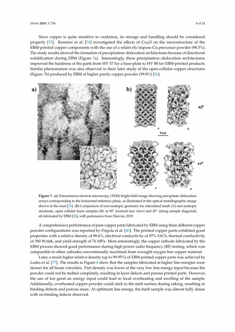
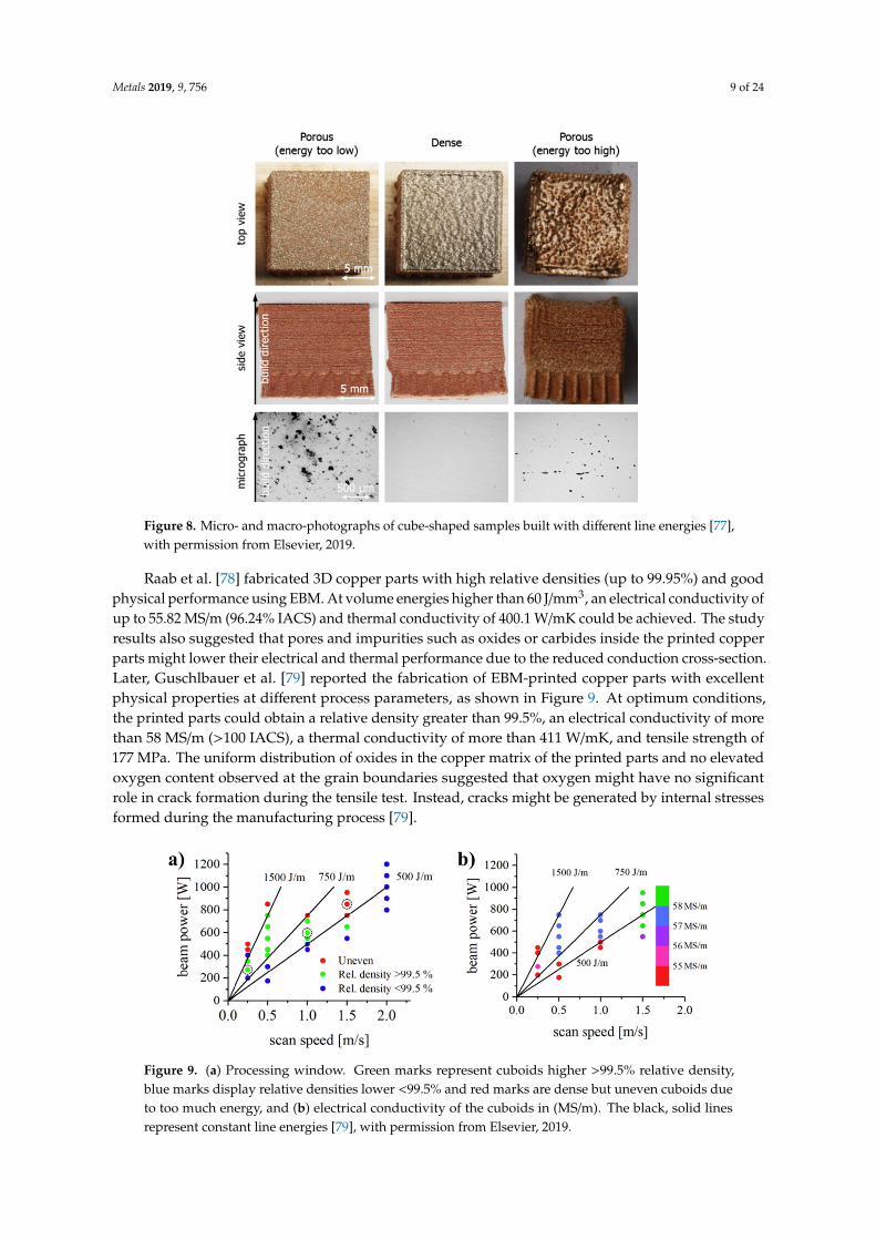
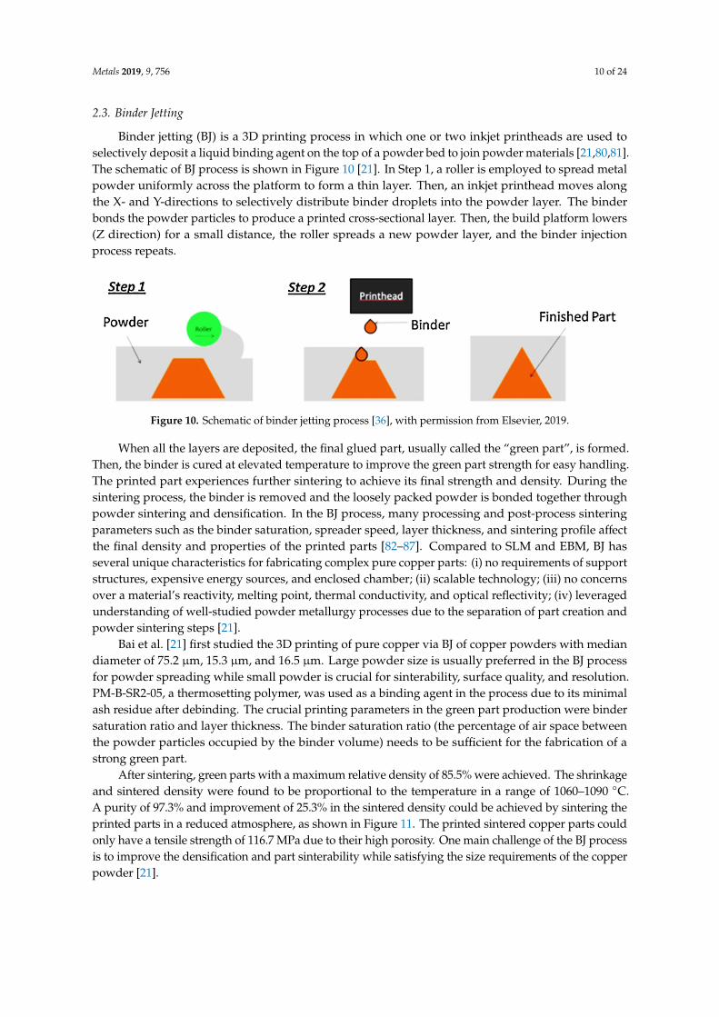
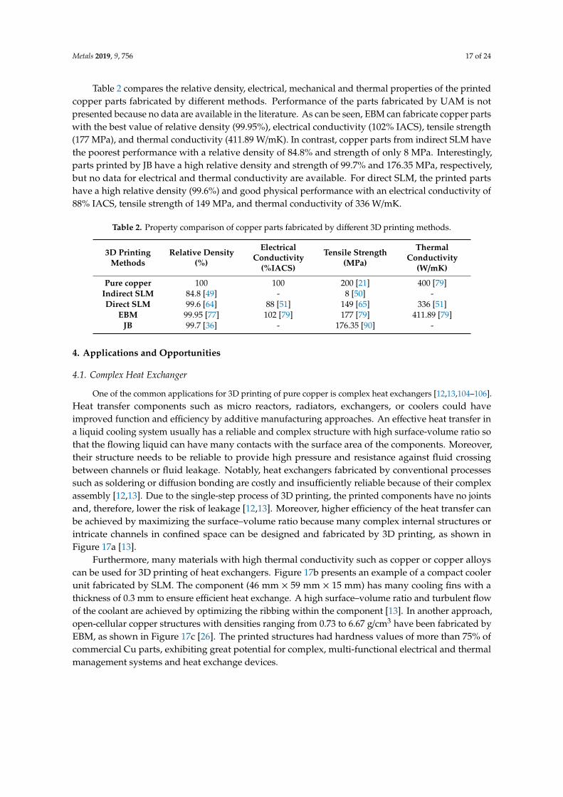
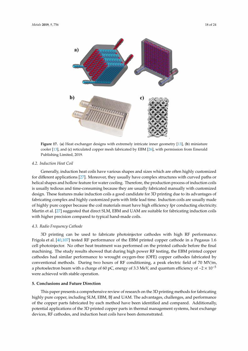
Related Documents