361 datapath.1 361 Computer Architecture Lecture 8: Designing a Single Cycle Datapath

361 datapath.1 361 Computer Architecture Lecture 8: Designing a Single Cycle Datapath.
Dec 19, 2015
Welcome message from author
This document is posted to help you gain knowledge. Please leave a comment to let me know what you think about it! Share it to your friends and learn new things together.
Transcript

361 datapath.1
361Computer Architecture
Lecture 8: Designing a Single Cycle Datapath

361 datapath.2
Outline of Today’s Lecture
° Introduction
° Where are we with respect to the BIG picture?
° Questions and Administrative Matters
° The Steps of Designing a Processor
° Datapath and timing for Reg-Reg Operations
° Datapath for Logical Operations with Immediate
° Datapath for Load and Store Operations
° Datapath for Branch and Jump Operations

361 datapath.3
The Big Picture: Where are We Now?
° The Five Classic Components of a Computer
° Today’s Topic: Design a Single Cycle Processor
Control
Datapath
Memory
ProcessorInput
Output
inst. set design technology
machinedesign Arithmetic
361 datapath.4
The Big Picture: The Performance Perspective° Performance of a machine is determined by:
• Instruction count
• Clock cycle time
• Clock cycles per instruction
° Processor design (datapath and control) will determine:
• Clock cycle time
• Clock cycles per instruction
° Today:
• Single cycle processor:
- Advantage: One clock cycle per instruction
- Disadvantage: long cycle time
CPI
Inst. Count Cycle Time

361 datapath.5
How to Design a Processor: step-by-step
° 1. Analyze instruction set => datapath requirements
• the meaning of each instruction is given by the register transfers
• datapath must include storage element for ISA registers
- possibly more
• datapath must support each register transfer
° 2. Select set of datapath components and establish clocking methodology
° 3. Assemble datapath meeting the requirements
° 4. Analyze implementation of each instruction to determine setting of control points that effects the register transfer.
° 5. Assemble the control logic
361 datapath.6
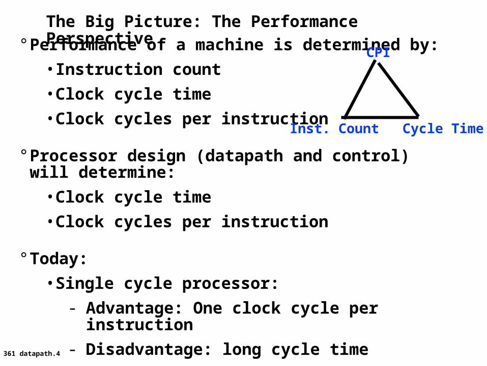
The MIPS Instruction Formats
° All MIPS instructions are 32 bits long. The three instruction formats:
• R-type
• I-type
• J-type
° The different fields are:
• op: operation of the instruction
• rs, rt, rd: the source and destination register specifiers
• shamt: shift amount
• funct: selects the variant of the operation in the “op” field
• address / immediate: address offset or immediate value
• target address: target address of the jump instruction
op target address
02631
6 bits 26 bits
op rs rt rd shamt funct
061116212631
6 bits 6 bits5 bits5 bits5 bits5 bits
op rs rt immediate
016212631
6 bits 16 bits5 bits5 bits

361 datapath.7
Step 1a: The MIPS-lite Subset for today
° ADD and SUB
• addU rd, rs, rt
• subU rd, rs, rt
° OR Immediate:
• ori rt, rs, imm16
° LOAD and STORE Word
• lw rt, rs, imm16
• sw rt, rs, imm16
° BRANCH:
• beq rs, rt, imm16
op rs rt rd shamt funct
061116212631
6 bits 6 bits5 bits5 bits5 bits5 bits
op rs rt immediate
016212631
6 bits 16 bits5 bits5 bits
op rs rt immediate
016212631
6 bits 16 bits5 bits5 bits
op rs rt immediate
016212631
6 bits 16 bits5 bits5 bits

361 datapath.8
Logical Register Transfers
° RTL gives the meaning of the instructions
° All start by fetching the instructionop | rs | rt | rd | shamt | funct = MEM[ PC ]
op | rs | rt | Imm16 = MEM[ PC ]
inst Register Transfers
ADDU R[rd] <– R[rs] + R[rt]; PC <– PC + 4
SUBU R[rd] <– R[rs] – R[rt]; PC <– PC + 4
ORi R[rt] <– R[rs] + zero_ext(Imm16); PC <– PC + 4
LOAD R[rt] <– MEM[ R[rs] + sign_ext(Imm16)]; PC <– PC + 4
STORE MEM[ R[rs] + sign_ext(Imm16) ] <– R[rt]; PC <– PC + 4
BEQ if ( R[rs] == R[rt] ) then PC <– PC + sign_ext(Imm16)] || 00
else PC <– PC + 4

361 datapath.9
Step 1: Requirements of the Instruction Set
° Memory
• instruction & data
° Registers (32 x 32)
• read RS
• read RT
• Write RT or RD
° PC
° Extender
° Add and Sub register or extended immediate
° Add 4 or extended immediate to PC

361 datapath.10
Step 2: Components of the Datapath
° Combinational Elements
° Storage Elements• Clocking methodology

361 datapath.11
Combinational Logic Elements (Basic Building Blocks)
° Adder
° MUX
° ALU
32
32
A
B32
Sum
Carry
32
32
A
B32
Result
OP
32A
B32
Y32
Select
Ad
der
MU
XA
LU
CarryIn

361 datapath.12
Storage Element: Register (Basic Building Block)
° Register
• Similar to the D Flip Flop except
- N-bit input and output
- Write Enable input
• Write Enable:
- negated (0): Data Out will not change
- asserted (1): Data Out will become Data In
Clk
Data In
Write Enable
N N
Data Out

361 datapath.13
Storage Element: Register File
° Register File consists of 32 registers:
• Two 32-bit output busses:
busA and busB
• One 32-bit input bus: busW
° Register is selected by:
• RA (number) selects the register to put on busA (data)
• RB (number) selects the register to put on busB (data)
• RW (number) selects the register to be writtenvia busW (data) when Write Enable is 1
° Clock input (CLK)
• The CLK input is a factor ONLY during write operation
• During read operation, behaves as a combinational logic block:
- RA or RB valid => busA or busB valid after “access time.”
Clk
busW
Write Enable
3232
busA
32busB
5 5 5RWRARB
32 32-bitRegisters

361 datapath.14
Storage Element: Idealized Memory
° Memory (idealized)
• One input bus: Data In
• One output bus: Data Out
° Memory word is selected by:
• Address selects the word to put on Data Out
• Write Enable = 1: address selects the memoryword to be written via the Data In bus
° Clock input (CLK)
• The CLK input is a factor ONLY during write operation
• During read operation, behaves as a combinational logic block:
- Address valid => Data Out valid after “access time.”
Clk
Data In
Write Enable
32 32DataOut
Address

361 datapath.15
Clocking Methodology
° All storage elements are clocked by the same clock edge
° Cycle Time = CLK-to-Q + Longest Delay Path + Setup + Clock Skew
Clk
Don’t Care
Setup Hold
.
.
.
.
.
.
.
.
.
.
.
.
Setup Hold
361 datapath.17
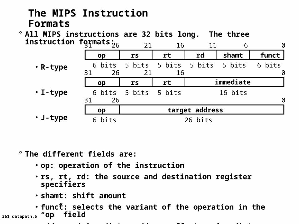
Step 3
° Register Transfer Requirements –> Datapath Assembly
° Instruction Fetch
° Read Operands and Execute Operation

361 datapath.18
3a: Overview of the Instruction Fetch Unit
° The common RTL operations
• Fetch the Instruction: mem[PC]
• Update the program counter:
- Sequential Code: PC <- PC + 4
- Branch and Jump: PC <- “something else”
32
Instruction WordAddress
InstructionMemory
PCClk
Next AddressLogic

361 datapath.19
RTL: The ADD Instruction
° add rd, rs, rt
• mem[PC] Fetch the instruction from memory
• R[rd] <- R[rs] + R[rt] The actual operation
• PC <- PC + 4 Calculate the next instruction’s address
op rs rt rd shamt funct
061116212631
6 bits 6 bits5 bits5 bits5 bits5 bits

361 datapath.20
RTL: The Subtract Instruction
° sub rd, rs, rt
• mem[PC] Fetch the instruction from memory
• R[rd] <- R[rs] - R[rt] The actual operation
• PC <- PC + 4 Calculate the next instruction’s address
op rs rt rd shamt funct
061116212631
6 bits 6 bits5 bits5 bits5 bits5 bits

361 datapath.21
3b: Add & Subtract
° R[rd] <- R[rs] op R[rt] Example: addU rd, rs, rt
• Ra, Rb, and Rw come from instruction’s rs, rt, and rd fields
• ALUctr and RegWr: control logic after decoding the instruction
32
Result
ALUctr
Clk
busW
RegWr
32
32
busA
32
busB
5 5 5
Rw Ra Rb
32 32-bitRegisters
Rs RtRd
AL
U
op rs rt rd shamt funct
061116212631
6 bits 6 bits5 bits5 bits5 bits5 bits

361 datapath.22
Datapath for Register-Register Operations (in general)
° R[rd] <- R[rs] op R[rt] Example: add rd, rs, rt
• Ra, Rb, and Rw comes from instruction’s rs, rt, and rd fields
• ALUctr and RegWr: control logic after decoding the instruction
32
Result
ALUctr
Clk
busW
RegWr
32
32
busA
32
busB
5 5 5
Rw Ra Rb
32 32-bitRegisters
Rs RtRd
AL
U
op rs rt rd shamt funct
061116212631
6 bits 6 bits5 bits5 bits5 bits5 bits
361 datapath.23
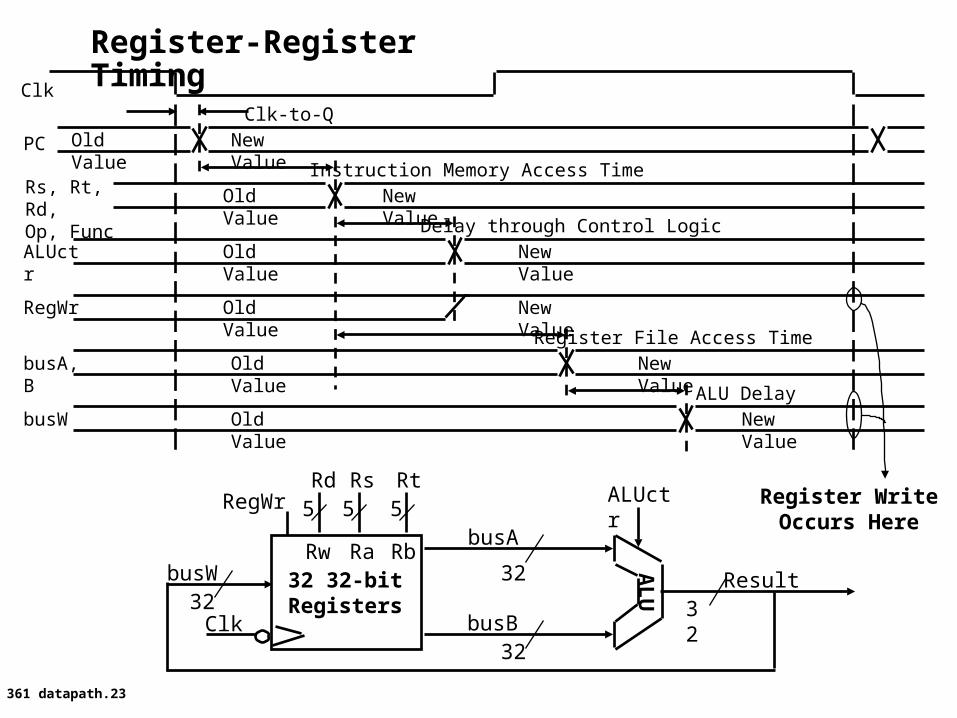
Register-Register Timing
32Result
ALUctr
Clk
busW
RegWr
3232
busA
32busB
5 5 5
Rw Ra Rb32 32-bitRegisters
Rs RtRd
AL
U
Clk
PC
Rs, Rt, Rd,Op, Func
Clk-to-Q
ALUctr
Instruction Memory Access Time
Old Value New Value
RegWr Old Value New Value
Delay through Control Logic
busA, B
Register File Access Time
Old Value New Value
busWALU Delay
Old Value New Value
Old Value New Value
New ValueOld Value
Register WriteOccurs Here

361 datapath.24
RTL: The OR Immediate Instruction
° ori rt, rs, imm16
• mem[PC] Fetch the instruction from memory
• R[rt] <- R[rs] or ZeroExt(imm16)
The OR operation
• PC <- PC + 4 Calculate the next instruction’s address
immediate
016 1531
16 bits16 bits
0 0 0 0 0 0 0 0 0 0 0 0 0 0 0 0
op rs rt immediate
016212631
6 bits 16 bits5 bits5 bits

361 datapath.25
3c: Logical Operations with Immediate° R[rt] <- R[rs] op ZeroExt[imm16] ]
32
Result
ALUctr
Clk
busW
RegWr
32
32
busA
32
busB
5 5 5
Rw Ra Rb
32 32-bitRegisters
Rs
RtRdRegDst
ZeroE
xt
Mu
x
Mux
3216imm16
ALUSrc
AL
U
11
op rs rt immediate
016212631
6 bits 16 bits5 bits5 bits rd?
immediate
016 1531
16 bits16 bits
0 0 0 0 0 0 0 0 0 0 0 0 0 0 0 0
361 datapath.26
RTL: The Load Instruction
° lw rt, rs, imm16
• mem[PC] Fetch the instruction from memory
• Addr <- R[rs] + SignExt(imm16)
Calculate the memory address
R[rt] <- Mem[Addr] Load the data into the register
• PC <- PC + 4 Calculate the next instruction’s address
immediate
016 1531
16 bits16 bits
0 0 0 0 0 0 0 0 0 0 0 0 0 0 0 0 0
016 1531
immediate
16 bits16 bits
1 1 1 1 1 1 1 1 1 1 1 1 1 1 1 1 1
op rs rt immediate
016212631
6 bits 16 bits5 bits5 bits

361 datapath.27
3d: Load Operations
° R[rt] <- Mem[R[rs] + SignExt[imm16]] Example: lw rt, rs, imm16
11
op rs rt immediate
016212631
6 bits 16 bits5 bits5 bits rd
32
ALUctr
Clk
busW
RegWr
32
32
busA
32
busB
5 5 5
Rw Ra Rb
32 32-bitRegisters
Rs
RtRd
RegDst
Exten
der
Mu
x
Mux
3216
imm16
ALUSrc
ExtOp
Clk
Data InWrEn
32
Adr
DataMemory
32
AL
U
MemWr Mu
x
W_Src
361 datapath.28
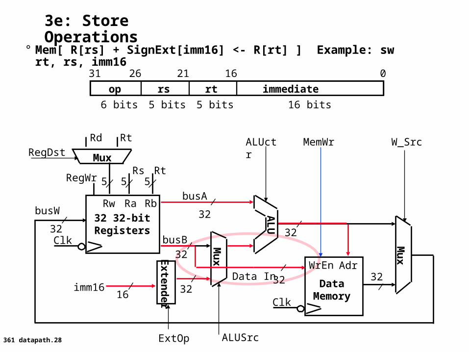
3e: Store Operations
° Mem[ R[rs] + SignExt[imm16] <- R[rt] ] Example: sw rt, rs, imm16
32
ALUctr
Clk
busW
RegWr
32
32
busA
32
busB
55 5
Rw Ra Rb
32 32-bitRegisters
Rs
Rt
Rt
Rd
RegDst
Exten
der
Mu
x
Mux
3216imm16
ALUSrcExtOp
Clk
Data InWrEn
32
Adr
DataMemory
MemWr
AL
U
op rs rt immediate
016212631
6 bits 16 bits5 bits5 bits
32
Mu
x
W_Src

361 datapath.29
3f: The Branch Instruction
° beq rs, rt, imm16
• mem[PC] Fetch the instruction from memory
• Equal <- R[rs] == R[rt] Calculate the branch condition
• if (COND eq 0) Calculate the next instruction’s address
- PC <- PC + 4 + ( SignExt(imm16) x 4 )
• else
- PC <- PC + 4
op rs rt immediate
016212631
6 bits 16 bits5 bits5 bits

361 datapath.30
Datapath for Branch Operations
° beq rs, rt, imm16 Datapath generates condition (equal)
op rs rt immediate
016212631
6 bits 16 bits5 bits5 bits
32
imm16
PC
Clk
00
Ad
der
Mu
x
Ad
der
4nPC_sel
Clk
busW
RegWr
32
busA
32
busB
5 5 5
Rw Ra Rb
32 32-bitRegisters
Rs Rt
Eq
ual
?
Cond
PC
Ext
Inst Address

361 datapath.31
Putting it All Together: A Single Cycle Datapath
imm
16
32
ALUctr
Clk
busW
RegWr
32
32
busA
32
busB
55 5
Rw Ra Rb
32 32-bitRegisters
Rs
Rt
Rt
RdRegDst
Exten
der
Mu
x
3216imm16
ALUSrcExtOp
Mu
x
MemtoReg
Clk
Data InWrEn32 Adr
DataMemory
MemWrA
LU
Equal
Instruction<31:0>
0
1
0
1
01
<21:25>
<16:20>
<11:15>
<0:15>
Imm16RdRtRs
=
Ad
der
Ad
der
PC
Clk
00
Mu
x
4
nPC_sel
PC
Ext
Adr
InstMemory

361 datapath.32
An Abstract View of the Critical Path° Register file and ideal memory:
• The CLK input is a factor ONLY during write operation
• During read operation, behave as combinational logic:
- Address valid => Output valid after “access time.”
Critical Path (Load Operation) = PC’s Clk-to-Q + Instruction Memory’s Access Time + Register File’s Access Time + ALU to Perform a 32-bit Add + Data Memory Access Time + Setup Time for Register File Write + Clock Skew
Clk
5
Rw Ra Rb
32 32-bitRegisters
RdA
LU
Clk
Data In
DataAddress
IdealData
Memory
Instruction
InstructionAddress
IdealInstruction
Memory
Clk
PC
5Rs
5Rt
16Imm
32
323232
A
B
Nex
t A
dd
ress

361 datapath.33
Binary Arithmetics for the Next Address
° In theory, the PC is a 32-bit byte address into the instruction memory:
• Sequential operation: PC<31:0> = PC<31:0> + 4
• Branch operation: PC<31:0> = PC<31:0> + 4 + SignExt[Imm16] * 4
° The magic number “4” always comes up because:
• The 32-bit PC is a byte address
• And all our instructions are 4 bytes (32 bits) long
° In other words:
• The 2 LSBs of the 32-bit PC are always zeros
• There is no reason to have hardware to keep the 2 LSBs
° In practice, we can simply the hardware by using a 30-bit PC<31:2>:
• Sequential operation: PC<31:2> = PC<31:2> + 1
• Branch operation: PC<31:2> = PC<31:2> + 1 + SignExt[Imm16]
• In either case: Instruction Memory Address = PC<31:2> concat “00”

361 datapath.34
Next Address Logic: Expensive and Fast Solution
° Using a 30-bit PC:
• Sequential operation: PC<31:2> = PC<31:2> + 1
• Branch operation: PC<31:2> = PC<31:2> + 1 + SignExt[Imm16]
• In either case: Instruction Memory Address = PC<31:2> concat “00”
3030
Sign
Ext
30
16imm16
Mu
x0
1
Ad
der
“1”
PC
ClkA
dd
er
30
30
Branch Zero
Addr<31:2>
InstructionMemory
Addr<1:0>“00”
32
Instruction<31:0>Instruction<15:0>
30
361 datapath.35
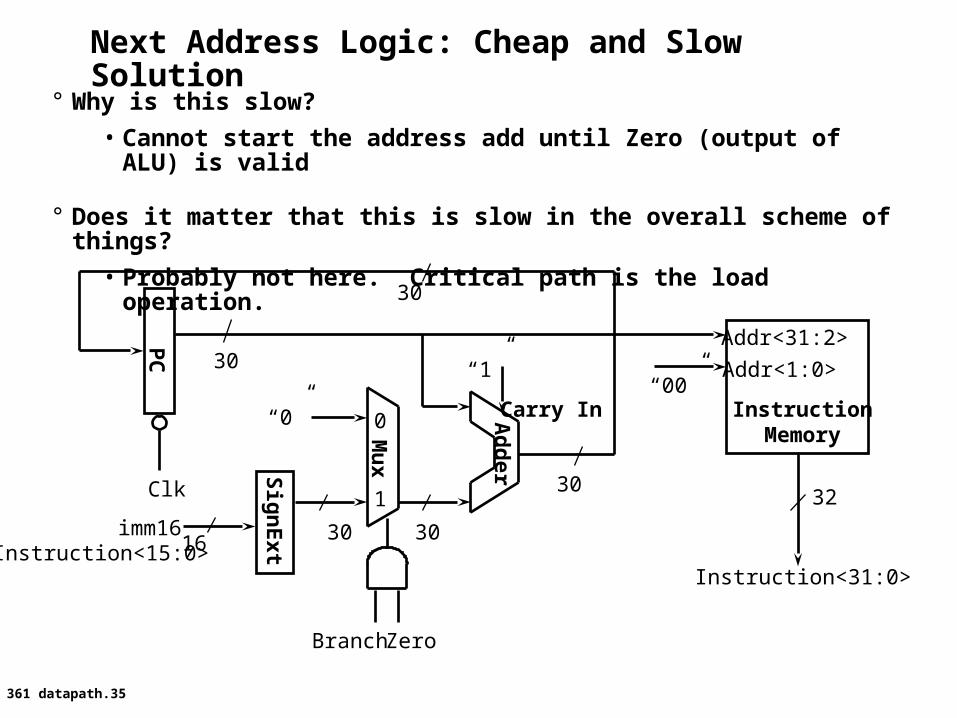
Next Address Logic: Cheap and Slow Solution
° Why is this slow?
• Cannot start the address add until Zero (output of ALU) is valid
° Does it matter that this is slow in the overall scheme of things?
• Probably not here. Critical path is the load operation.
30
30Sign
Ext 3016
imm16
Mu
x
0
1
Ad
der
“0”
PC
Clk
30
Branch Zero
Addr<31:2>
InstructionMemory
Addr<1:0>“00”
32
Instruction<31:0>
30
“1”
Carry In
Instruction<15:0>

361 datapath.36
RTL: The Jump Instruction
° j target
• mem[PC] Fetch the instruction from memory
• PC<31:2> <- PC<31:28> concat target<25:0>
Calculate the next instruction’s address
op target address
02631
6 bits 26 bits

361 datapath.37
Instruction Fetch Unit
3030
Sign
Ext
30
16imm16
Mu
x
0
1
Ad
der
“1”
PC
Clk
Ad
der
30
30
Branch Zero
“00”
Addr<31:2>
InstructionMemory
Addr<1:0>
32
Mu
x1
0
26
4
PC<31:28>
Target30
° j target
• PC<31:2> <- PC<31:28> concat target<25:0>
Jump
Instruction<15:0>
Instruction<31:0>
30
Instruction<25:0>

361 datapath.38
Putting it All Together: A Single Cycle Datapath
32
ALUctr
Clk
busW
RegWr
32
32
busA
32
busB
55 5
Rw Ra Rb
32 32-bitRegisters
Rs
Rt
Rt
RdRegDst
Exten
der
Mu
x
Mux
3216imm16
ALUSrc
ExtOp
Mu
x
MemtoReg
Clk
Data InWrEn
32
Adr
DataMemory
32
MemWrA
LU
InstructionFetch Unit
Clk
Zero
Instruction<31:0>
Jump
Branch
° We have everything except control signals (underline)
0
1
0
1
01<
21:25>
<16:20>
<11:15>
<0:15>
Imm16RdRsRt

361 datapath.39
An Abstract View of the Implementation
° Logical vs. Physical Structure
DataOut
Clk
5
Rw Ra Rb
32 32-bitRegisters
Rd
AL
U
Clk
Data In
DataAddress
IdealData
Memory
Instruction
InstructionAddress
IdealInstruction
Memory
Clk
PC
5Rs
5Rt
32
323232
A
B
Nex
t A
dd
ress
Control
Datapath
Control Signals Conditions

361 datapath.41
Summary
° 5 steps to design a processor• 1. Analyze instruction set => datapath requirements
• 2. Select set of datapath components & establish clock methodology
• 3. Assemble datapath meeting the requirements
• 4. Analyze implementation of each instruction to determine setting of control points that effects the register transfer.
• 5. Assemble the control logic
° MIPS makes it easier• Instructions same size
• Source registers always in same place
• Immediates same size, location
• Operations always on registers/immediates
° Single cycle datapath => CPI=1, CCT => long
° Next time: implementing control (Steps 4 and 5)
Related Documents