MIT OpenCourseWare http://ocw.mit.edu 3.23 Electrical, Optical, and Magnetic Properties of Materials Fall 2007 For information about citing these materials or our Terms of Use, visit: http://ocw.mit.edu/terms.

Welcome message from author
This document is posted to help you gain knowledge. Please leave a comment to let me know what you think about it! Share it to your friends and learn new things together.
Transcript

MIT OpenCourseWare http://ocw.mit.edu
3.23 Electrical, Optical, and Magnetic Properties of MaterialsFall 2007
For information about citing these materials or our Terms of Use, visit: http://ocw.mit.edu/terms.

3.23 Fall 2007 – Lecture 14
INHOMOGENEOUS SEMICONDCUTORS
Russell Ohl Shockley, Bardeen, and Brattain 3.23 Electronic, Optical and Magnetic Properties of Materials - Nicola Marzari (MIT, Fall 2007)
William Shockley
Electronic Bands in Sodium Chloride
(advisor John C. Slater, MIT, 1936)
3.23 Electronic, Optical and Magnetic Properties of Materials - Nicola Marzari (MIT, Fall 2007)
1
Images removed due to copyright restrictions.
http://dspace.mit.edu/handle/1721.1/10879
3.23 Electronic, Optical and Magnetic Properties of Materials Nicola Marzari (MIT, Fall 2007)
3.23 Electronic, Optical and Magnetic Properties of Materials Nicola Marzari (MIT, Fall 2007)
-
-
2

•
Last time
1. Band structure of direct- and indirect-gap semiconductors, in excruciating detailin excruciating detail
2. Carriers in thermal equilibrium, density of available states
3. Law of mass action
4. Consequences for intrinsic semiconductors, extrinsic semiconductors
5. Impurity levels, hydrogen model of donors, acceptor states
6. Temperature dependence of majority carriers: intrinsic range, extrinsic/saturation range, freeze out.
3.23 Electronic, Optical and Magnetic Properties of Materials - Nicola Marzari (MIT, Fall 2007)
Study
• Early part of Chap 29 (InhomogeneousEarly part of Chap 29 (Inhomogeneous semiconductors) ,Ashcroft-Mermin (to be posted, together with Chap 28, really to be posted, s'il vous plaît)
3.23 Electronic, Optical and Magnetic Properties of Materials - Nicola Marzari (MIT, Fall 2007)
3

Density of available states
2.5= ⎛ mc ⎞3/2 ⎛ T ⎞
3/2 19 3
⎜ ⎟ ⎜ ⎟ 10 / cm ⎝ m ⎠ ⎝ 300 K ⎠
3.23 Electronic, Optical and Magnetic Properties of Materials - Nicola Marzari (MIT, Fall 2007)
Law of Mass Action
−E k T n p = N Pe g / Bc v c v
3.23 Electronic, Optical and Magnetic Properties of Materials - Nicola Marzari (MIT, Fall 2007)
4
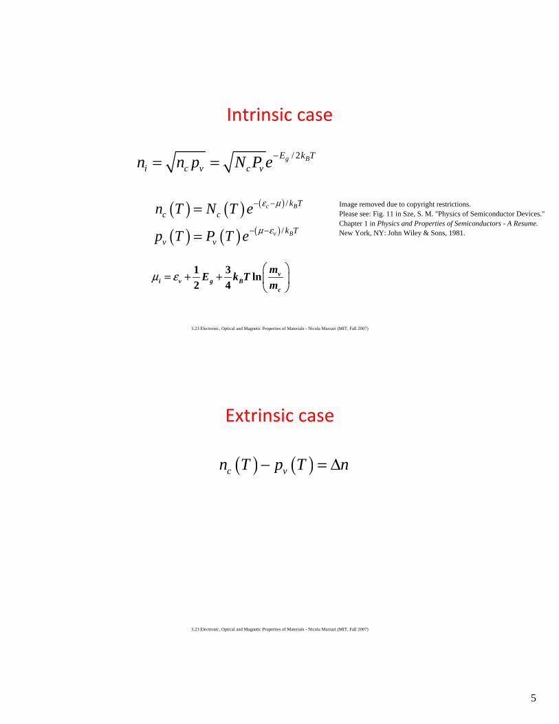
Intrinsic case
Bnii = ncc ppvv = N Pc v c v e −Eg / 2k T
c ( ) = c ( ) (ε µ− ) / Bn T N T e − c k T
( ) v ( ) − −(µ εv ) / k TBp T = P T e v
1 3 ⎛ m ⎞ µ = ε + E + k T lni v 2 g 4 B ⎝⎜ m
v
c ⎠⎟
3.23 Electronic, Optical and Magnetic Properties of Materials - Nicola Marzari (MIT, Fall 2007)
Extrinsic case
n T(( )) − pp ((T )) = ∆ncc vv
3.23 Electronic, Optical and Magnetic Properties of Materials - Nicola Marzari (MIT, Fall 2007)
5
Image removed due to copyright restrictions. Please see: Fig. 11 in Sze, S. M. "Physics of Semiconductor Devices." Chapter 1 in Physics and Properties of Semiconductors - A Resume.New York, NY: John Wiley & Sons, 1981.
Extrinsic case
3.23 Electronic, Optical and Magnetic Properties of Materials - Nicola Marzari (MIT, Fall 2007)
Temperature dependence of majority carriers
3.23 Electronic, Optical and Magnetic Properties of Materials - Nicola Marzari (MIT, Fall 2007)
6
Image removed due to copyright restrictions. Please see Fig. 13.3 in Kittel, Charles, and Herbert Kroemer. Thermal Physics. San Francisco, CA: W. H. Freeman, 1980.
Image removed due to copyright restrictions. Please see Fig. 2.22 in Pierret, Robert F. Semiconductor Device Fundamentals. Reading, MA: Addison-Wesley, 1996.
Impurity types, levels
Population of impurity levels (donor)
3.23 Electronic, Optical and Magnetic Properties of Materials - Nicola Marzari (MIT, Fall 2007)
7
Image removed due to copyright restrictions.
Please see: Fig. 13 in Sze, S. M. "Physics of Semiconductor Devices." Chapter 1 in Physics and Properties of Semiconductors - A Resume. New York, NY: John Wiley & Sons, 1981.
-3.23 Electronic, Optical and Magnetic Properties of Materials - Nicola Marzari (MIT, Fall 2007)
Population of impurity levels (acceptor)
3.23 Electronic, Optical and Magnetic Properties of Materials - Nicola Marzari (MIT, Fall 2007)
Conductivity in semiconductors eτ eτσ = n e e + n e h
e hme mh
eeττ µe = e
me
eτ hµh = me
3.23 Electronic, Optical and Magnetic Properties of Materials - Nicola Marzari (MIT, Fall 2007)
8
Text removed due to copyright restrictions.
Please see: Table 3 in Kittel, Charles. "Introduction to Solid State Physics." Chapter 8 in Semiconductor Crystals. New York, NY: John Wiley & Sons, 2004.

Impurity band conduction
3.23 Electronic, Optical and Magnetic Properties of Materials - Nicola Marzari (MIT, Fall 2007)
Equilibrium carrier densities of impure semiconductors
3.23 Electronic, Optical and Magnetic Properties of Materials - Nicola Marzari (MIT, Fall 2007)
9
–
Equilibrium carrier densities of impure semiconductors
3.23 Electronic, Optical and Magnetic Properties of Materials - Nicola Marzari (MIT, Fall 2007)
Semiconductor carrier engineering
• Adding impurities to determine carrier typeni
2 3n 2 for Si: ~1020cm-3 for Si: 1020cm – Add 1016cm-3 (~1ppm) phosphorous (donors) to Si: nc~Nd
– nc~1016cm-3, pv~104 (ni2/Nd)
• Adding impurities to change carrier density – 1 part in 106 impurity in a crystal (~1022cm-3 atom density) – 1022/ 106 =1016 dopant atoms per cm-3
– conductivity is proportional to the # of carriers leading to 6 orders of magnitude change in conductivity! of magnitude change in conductivity!
Impurities at the ppm level drastically change the conductivity (5-6 orders of
magnitude)
3.23 Electronic, Optical and Magnetic Properties of Materials - Nicola Marzari (MIT, Fall 2007)
10

Simplified expressions
3.23 Electronic, Optical and Magnetic Properties of Materials - Nicola Marzari (MIT, Fall 2007)
Abrupt junction
3.23 Electronic, Optical and Magnetic Properties of Materials - Nicola Marzari (MIT, Fall 2007)
11
Image removed due to copyright restrictions.Please see: Fig. 29.1 in Ashcroft, Neil W., and Mermin, N. David.Solid State Physics. Belmont, CA: Brooks/Cole, 1976.

The p-n junction (diode)
p-type material at equilibrium n-type material at equilibrium
p~NAn~ND
n~ni2/N p~ni
2/N
µ = µA − k T ln ⎛ NA
⎞ µ = µD+ k T ln ⎛ ND
⎞ p i b ⎜ ⎟ n i b ⎜ ⎟
⎝ ni ⎠ ⎝ ni ⎠
E Ec Ec
µ µ Ev Ev
What happens when you join these together?
12
Joining p and n p n
Ecc µ
Ev Carriers flow under driving force of diffusion until µ is horizontal
- -+
+
--++ +
Holes diffuse Electrons diffuse
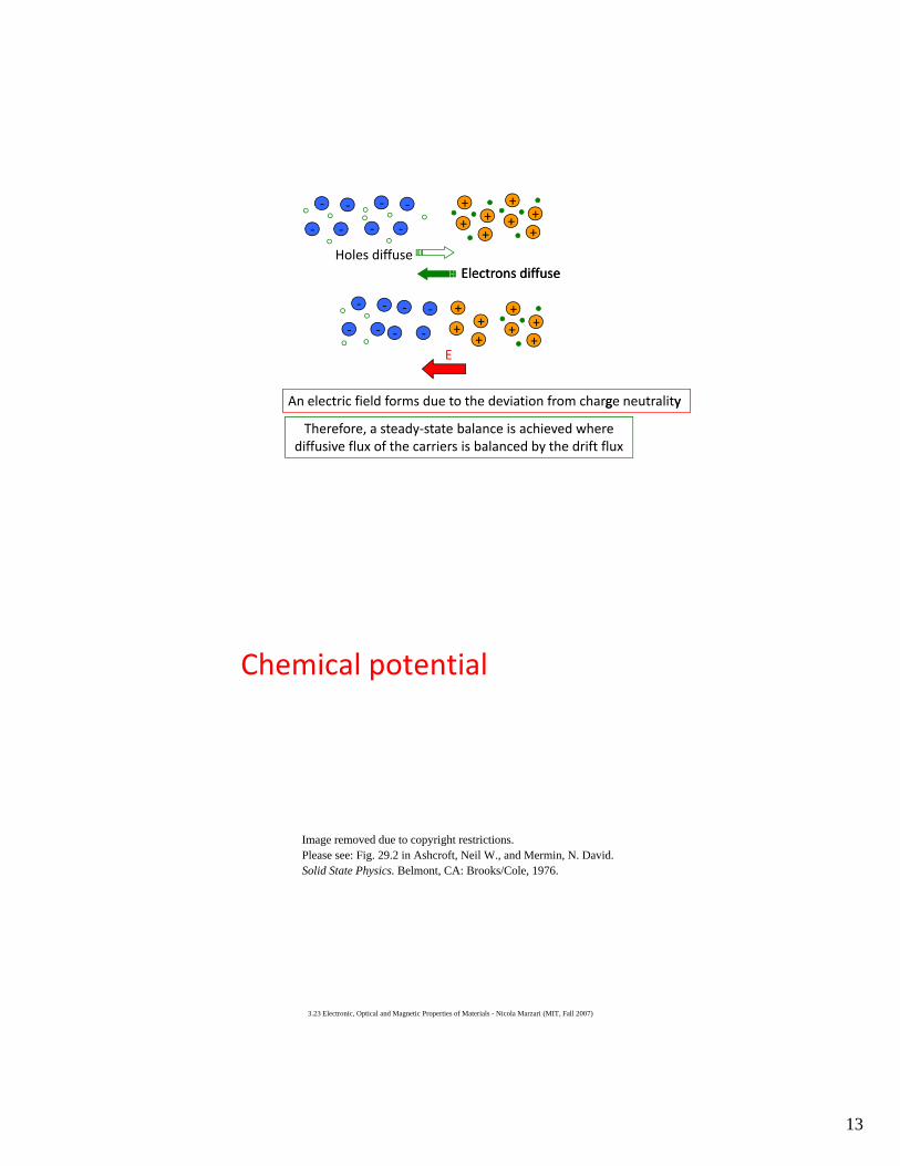
Chemical potential
3.23 Electronic, Optical and Magnetic Properties of Materials - Nicola Marzari (MIT, Fall 2007)
An electric field forms due to the deviation from chargg e neutralityy
Therefore, a steady-state balance is achieved where diffusive flux of the carriers is balanced by the drift flux
Image removed due to copyright restrictions.Please see: Fig. 29.2 in Ashcroft, Neil W., and Mermin, N. David.Solid State Physics. Belmont, CA: Brooks/Cole, 1976.
13
-
--
-++ +
+
Holes diffuse Electrons diffuse
++ +
+-
--
-
Electrons diffuse
-
--
-++ +
+ -
--
-++ +
+
E

Carrier concentration in a p-n junction
14
Images removed due to copyright restrictions. Please see
http://commons.wikimedia.org/wiki/Image:Pn-junction-equilibrium.svg
http://commons.wikimedia.org/wiki/Image:Pn-junction-equilibrium-graphs.png p-n

What is the built-in voltage Vbi?
p nn
Ecµ
Ev
qVbi=µn- µp
ln D n i b
Nk Tµ µ ⎛ ⎞
= + ⎜ ⎟ln a p i b
Nk Tµ µ ⎛ ⎞
= − ⎜ ⎟
nn
pn p
qVbi
qVb
i
n i b in
µ µ ⎜ ⎟ ⎝ ⎠
p i b in
µ µ ⎜ ⎟ ⎝ ⎠
2lnb a d bi
i
k T N N V q n
⎛ ⎞∴ = ⎜ ⎟
⎝ ⎠
p
p
15
dbio
--
- - - - + + - - + + + +
+ +
xp xn Metallurgical
W dW: deplletion or space chharge width junctionti idth junction
r
Nd xn = Na xp
E = ∫ρ(x)dx
E ε x == 2ε rεoVbi Nxp e Na (Nd + Na )
V x 2ε rεoVbi Na=
Vbi n e Nd (Nd + Na )
V E x d( ) x= −∫
d

Operation under bias
3.23 Electronic, Optical and Magnetic Properties of Materials - Nicola Marzari (MIT, Fall 2007)
Rectification
3.23 Electronic, Optical and Magnetic Properties of Materials - Nicola Marzari (MIT, Fall 2007)
16
Image removed due to copyright restrictions.Please see: Fig. 29.4 in Ashcroft, Neil W., and Mermin, N. David.Solid State Physics. Belmont, CA: Brooks/Cole, 1976.
Image removed due to copyright restrictions.Please see: Fig. 29.5 in Ashcroft, Neil W., and Mermin, N. David.Solid State Physics. Belmont, CA: Brooks/Cole, 1976.
Related Documents