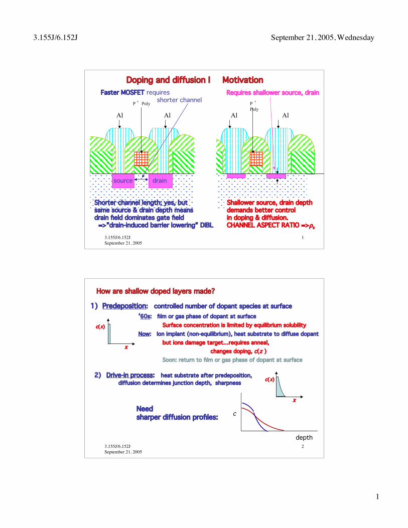
3.155J/6.152J September 21, 2005, Wednesday 1 3.155J/6.152J September 21, 2005 1 P + Poly Al Al P + Poly Al Al Doping and diffusion I Motivation Shorter channel length; yes, but same source & drain depth means drain field dominates gate field =>”drain-induced barrier lowering” DIBL drain source Faster MOSFET requires shorter channel Requires shallower source, drain Shallower source, drain depth demands better control in doping & diffusion. CHANNEL ASPECT RATIO =>ρ s 3.155J/6.152J September 21, 2005 2 Need sharper diffusion profiles: c depth How are shallow doped layers made? 1) Predeposition : controlled number of dopant species at surface ‘60s : film or gas phase of dopant at surface Surface concentration is limited by equilibrium solubility Now : Ion implant (non-equilibrium), heat substrate to diffuse dopant but ions damage target…requires anneal, changes doping, c(z ) Soon: return to film or gas phase of dopant at surface c(x) x 2) Drive-in process : heat substrate after predeposition, diffusion determines junction depth, sharpness c(x) x

Welcome message from author
This document is posted to help you gain knowledge. Please leave a comment to let me know what you think about it! Share it to your friends and learn new things together.
Transcript
3.155J/6.152J September 21, 2005, Wednesday
1
3.155J/6.152JSeptember 21, 2005
1
P + Poly
AlAl
P +
PolyAlAl
Doping and diffusion I Motivation
Shorter channel length; yes, but same source & drain depth meansdrain field dominates gate field =>”drain-induced barrier lowering” DIBL
drainsource
Faster MOSFET requires shorter channel
Requires shallower source, drain
Shallower source, drain depth demands better control in doping & diffusion.CHANNEL ASPECT RATIO =>ρs
3.155J/6.152JSeptember 21, 2005
2
Need sharper diffusion profiles: c
depth
How are shallow doped layers made?
1) Predeposition: controlled number of dopant species at surface‘60s: film or gas phase of dopant at surface
Surface concentration is limited by equilibrium solubility Now: Ion implant (non-equilibrium), heat substrate to diffuse dopant
but ions damage target…requires anneal, changes doping, c(z )
Soon: return to film or gas phase of dopant at surface
c(x)
x
2) Drive-in process: heat substrate after predeposition, diffusion determines junction depth, sharpness c(x)
x
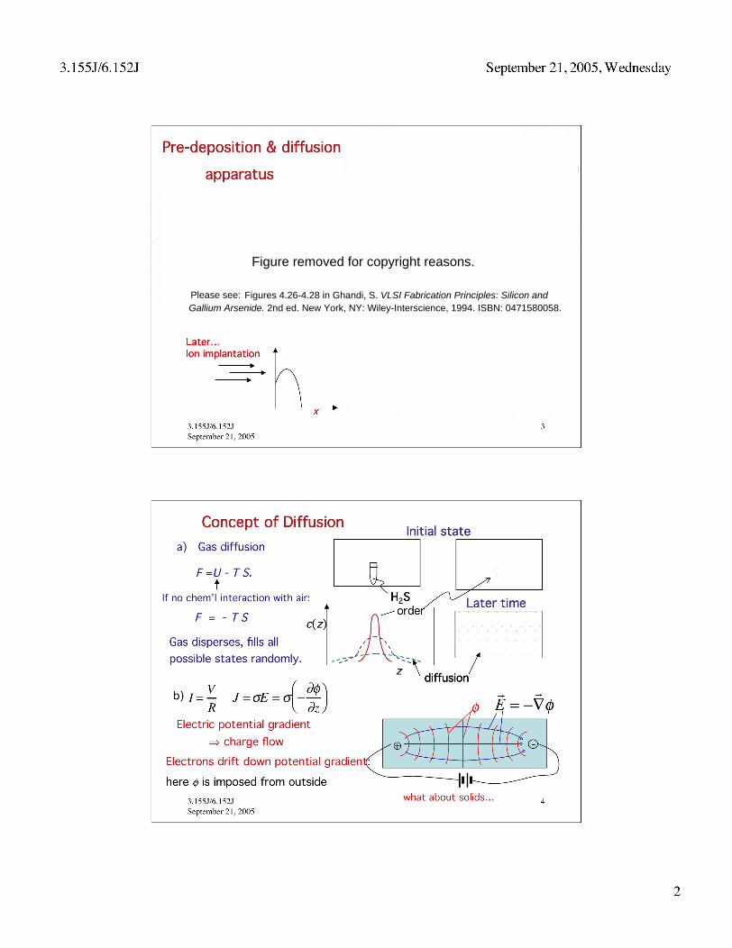
Figures 4.26-4.28 in Ghandi, S. VLSI Fabrication Principles: Silicon and Gallium Arsenide. 2nd ed. New York, NY: Wiley-Interscience, 1994. ISBN: 0471580058.
Figure removed for copyright reasons.
Please see:

3.155J/6.152J September 21, 2005, Wednesday
3
3.155J/6.152JSeptember 21, 2005
5
c) Mass (or heat) flow JJ,
due to concentration gradient
J #area � t( ) = D �
�c�z
���
�� FFiicckk II
t > 0
J = 0c( z, t )
z
d)
z�z
J in = J z( ) Jout = J z + �z( )z z+�z dC z( )
dt�z = +J z( ) � J z + �z( ) #
area � t
dC
dt=J z( ) � J z + �z( )
�z�z�0� ���� �
dJ
dz
TThheessee EEqqss ==>> ttiimmee eevvoolluuttiioonn ooff ssoommee iinniittiiaall ccoonnddiittiioonnss && bboouunnddaarryy ccoonnddiittiioonnss
dC(z)
dt= �
d
dzD �
�C�z
��
��
…or if D is constantdC z, t( )dt
=D�2C z,t( )
FFiicckk IIII
Time dep. Schrödinger Eq.
+ih���t
= �h2
2m� 2� + V�
Diffusingspeciesmust besolubleIn host
Inflow out
3.155J/6.152JSeptember 21, 2005
6
AAttoommiissttiicc ppiiccttuurree ooff ddiiffffuussiioonn iinn ssoolliiddssSSeeee wweebb ssiittee ffoorr mmoovviieess::http://www.tf.uni-kiel.de/matwis/amat/def_en/index.html
Most important is vvaaccaannccyy ddiiffffuussiioonn.
Ea
i f
En
Initial and final states have same energy
Also possible is direct exchange (�� = bbrrookkeenn bboonndd))
Higher energy barrier or break more bonds => lower value of D =D0 exp �E kT( )
����
����
3.155J/6.152J September 21, 2005, Wednesday
4
3.155J/6.152JSeptember 21, 2005
7
2 stepsfor diffusion: 1) create vacancy 2) achieve energy Ea
nv
=N
v
N0
= exp !2.6
kT
"
# $
%
& '
!v
= !0 exp " Ea
kT
#
$ %
&
' (
cm2
s
!
"
# $
%
&
!3
2
kBT
h= 9 "10
12s#1$10
13s#1
Atomistic picture of vacancy diffusion
D ~ a x v
= a2! 0 exp "
Ev
+ Ea
kT
#
$ %
&
' (
D = D0 exp !EVD
kT
"
#
$
%
Contains ν0 ≈ Debye frequency
EVD
a
ν0
Vacancy diffusion
3.155J/6.152JSeptember 21, 2005
8
1022 1021 1020 1019 1018 1017 1016
Impurity content (cm-3)
100 at% 10 at%
Solubility limits
1.0
T/Tm
Si at% dopant
Liquid
Liq + Sol
Solubility dopant in Si Solid
Sample phase diagram 1.0
T/Tm
1020 1021 Impurity content (cm-3)
B As P
From phase diagram:

3.155J/6.152J September 21, 2005, Wednesday
5
3.155J/6.152JSeptember 21, 2005
9
Solubility limits
3.155J/6.152JSeptember 21, 2005
10
Analytic Solution to Diffusion Equations, Fick II:
!C
!t= D
!2C
!z2
In oxidation we assumed steady state :
O2 diffusion through SiO2 , where
flux is same everywhere.
Not necessarily so in diffusion where
non-linear c(z) can exist and be frozen in at D = 0
,J = !D"C
"z= !Db,
There are many different solutions to this or any DE; the correct solution is the one that satisfies the BC.
Implies either a) D = 0 c(z) may be curved
Steady state, dc/dt = 0
C(z) = a + bz
z ∞0
C(z)
or b) d2c/dz2 = 0 c(x) linear
Figure 2-4 in Campbell, S. The Science and Engineering of Microelectronic Fabrication. 1st ed. New York, NY: Oxford University Press, 1996. ISBN: 0195105087.
Figure removed for copyright reasons.
Please see:
3.155J/6.152J September 21, 2005, Wednesday
6
3.155J/6.152JSeptember 21, 2005
11
BBCC IICC
BBCC
Diffusion couple: thin dopant layer on rod face,
press 2 identical pieces together, heat.
Then study diffusion profile in sections.
For solutions, boundary condition, consider classical experiment:
symmetry
z �0
t = 0
dC 0,t( )dz
= 0
C �,t( ) = 0
C z,0( ) = 0 z � 0( )
C z, t( )��
�
� dz =Q = const. (# /area)
3.155J/6.152JSeptember 21, 2005
12
AAnnaallyyttiicc SSoolluuttiioonn ttoo DDiiffffuussiioonn EEqquuaattiioonnss J = �D�c�z
,�c�t
= D� 2c
�z2
t = 0
dc 0,t( )dz
= 0
c �,t( ) = 0
c z,0( ) = 0 z � 0( )
z �0
I. “ Drive in” of fixed amount, Q, of dopant; solution is Gaussian
PPrreeddeeppoossiittiioonn iiss
ddeellttaa ffuunnccttiioonn,, ��((zz))..
C z,t( ) = Q
�Dtexp �
z 2
4Dt
�
���
��t > 0 UUnniittss
Width of Gaussian = = diffusion length a
(a is large relative to width of predeposition)
1
2 a = 2 Dt
DDoossee,, QQ,, aammoouunntt ooff ddooppaanntt iinn ssaammppllee,, iiss ccoonnssttaanntt.. C z, t( )��
�
� dz =Q = const. (# /area)
c z,t( ) = constexp �z2
4Dt
�
��
�
��
##//vvooll == QQ//((lleennggtthh22))11//22
SSoo QQ hhaass uunniittss ##//aarreeaa

3.155J/6.152J September 21, 2005, Wednesday
7
3.155J/6.152JSeptember 21, 2005
13
erf
t = 0C
0
Solutions for other I.C./B.C. can be obtained by superposition:
II. Limitless source
of dopant(e.g. growth inpresence of vapor)
! 2 =z2
4Dt"(z # z
0)2
4Dt
Cimp z, t( ) =2
!exp "# 2[ ]
0
u=z
2 Dt
$ d# % erf u( ) = erfz
2 Dt
&
'
(
)
C (∞, t )
C 0, t( ) = C0
C z,0( ) = 0
z
Const C0
t
C !,t( ) = 0
0
BC
IC BC
3.155J/6.152JSeptember 21, 2005
14
Other I.C./B.C. (cont.):
C z,t( ) = Csurferfc
z
2 Dt
!
" # $
% & ,t > 0
a = diffusion length
= 2 Dt
(D ≈ 10-15) × (t = 103) ⇒ a ≈ 0.2 µm
erfc u( ) =1! erf u( )
z
c
z
erf z( )
0 1 2
1 0.995
c(∞, t) = 0
C 0, t( ) = C0
C z,0( ) = 0
z
Const c0
t
Dose !Q = C(z,t)dz =2 Dt
"0
#
$ C0
=a
!C0
c0 limited by solid solubility
Dose, Q,amount of dopantin sample,increases as t1/2.
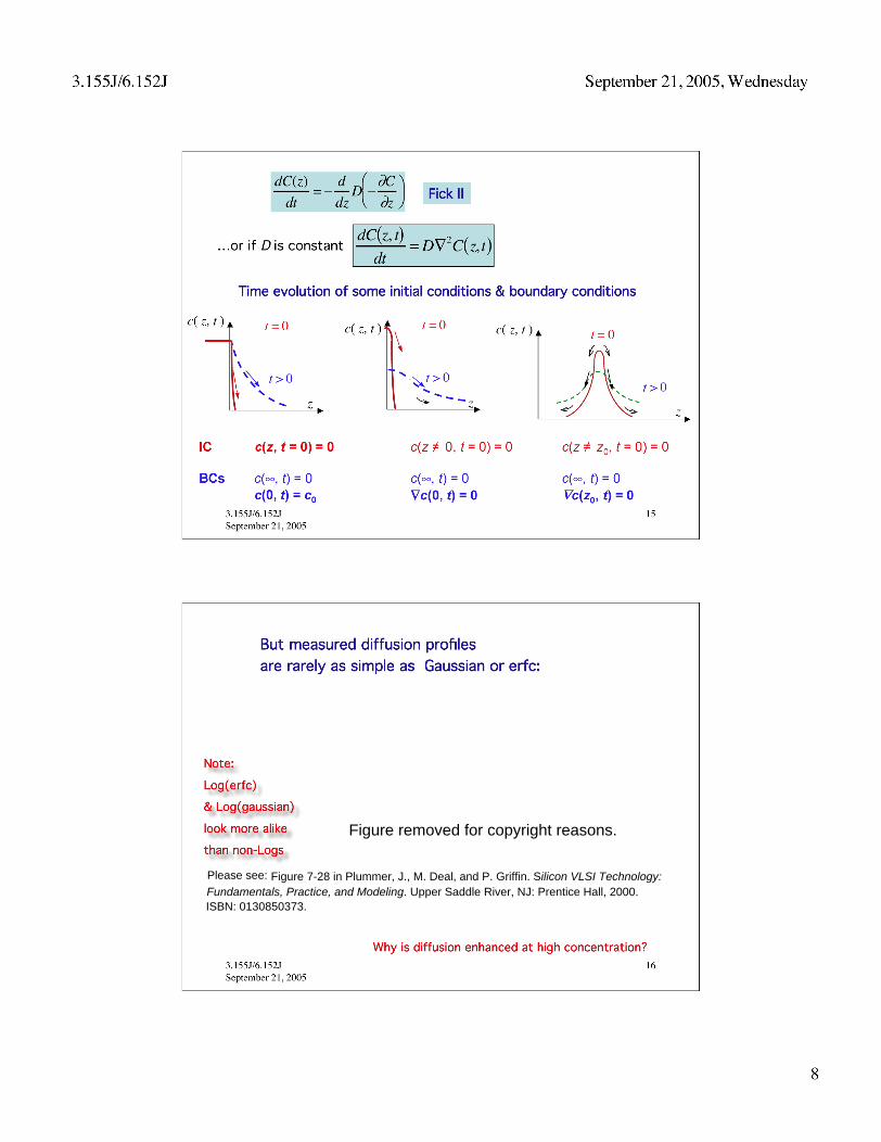
Figure 7-28 in Plummer, J., M. Deal, and P. Griffin. Silicon VLSI Technology: Fundamentals, Practice, and Modeling. Upper Saddle River, NJ: Prentice Hall, 2000. ISBN: 0130850373.
Figure removed for copyright reasons.
Please see:
3.155J/6.152J September 21, 2005, Wednesday
9
3.155J/6.152JSeptember 21, 2005
17
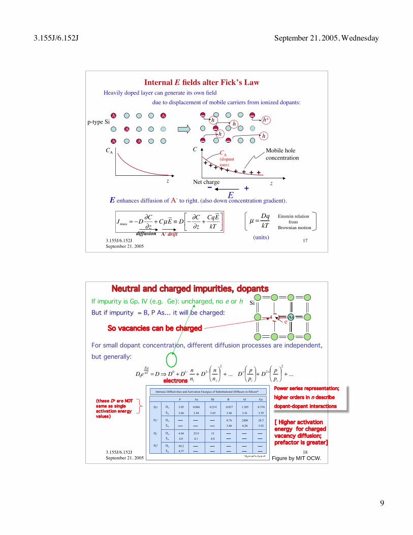
Heavily doped layer can generate its own fielddue to displacement of mobile carriers from ionized dopants:
p-type SiA A
A
A A
z
CA
+ + + + + + + + +z
C CA(dopantions)
Mobile holeconcentration
Net charge- +EE enhances diffusion of A- to right, (also down concentration gradient).
Internal E fields alter Fick’s Law
Jmass
= !D"C
"z+ CµE
!"# D !
"C
"z+CqE!"
kT
$
%&
'
()
diffusion A- drift
µ =Dq
kT
Einstein relation from Brownian motion
− −
−
− −
h hh h
h+
(units)
3.155J/6.152JSeptember 21, 2005
18
Neutral and charged impurities, dopantsIf impurity is Gp. IV (e.g. Ge): uncharged, no e or h
But if impurity = B, P As… it will be charged:
[ Higher activationenergy for chargedvacancy diffusion;prefactor is greater]
So vacancies can be chargedAs
e-
Si
electronsholes
For small dopant concentration, different diffusion processes are independent,
but generally:
D0e
Ea
kT = D! D0
+ D1" n
ni+ D
2" n
ni
#
$
% &
'
(
2
+ ... D+ p
pi
#
$
% &
'
( + D2+ p
pi
#
$
% &
'
(
2
+ ...
(these Do are NOTsame as singleactivation energyvalues)
Power series representation;
higher orders in n describe
dopant-dopant interactions
Figure by MIT OCW.
Dio Do
Eo
Do
Eo
Do
Eo
Do
Eo
Di+
Di-
Di2
3.85
3.66
4.44
4.0
44.2
4.37
0.066
3.44
22.9
4.1
0.214
3.65
13
4.0
0.037
3.46
0.76
3.46
1.385
3.41
2480
4.20
0.374
3.39
28.5
3.92
P As Sb B Al Ga
* D0 in cm2/s; E0 in eV.
Intrinsic Diffusivities and Activation Energies of Substitutional Diffusers in Silicon*
3.155J/6.152J September 21, 2005, Wednesday
10
3.155J/6.152JSeptember 21, 2005
19
Doff
= D0
+ D! n
ni
"
#
$ $
%
&
' ' + D2! n
ni
"
#
$ $
%
&
' '
2
+ ...+ D+ p
ni
"
#
$ $
%
&
' ' + D2+ p
ni
"
#
$ $
%
&
' '
2
+ ...
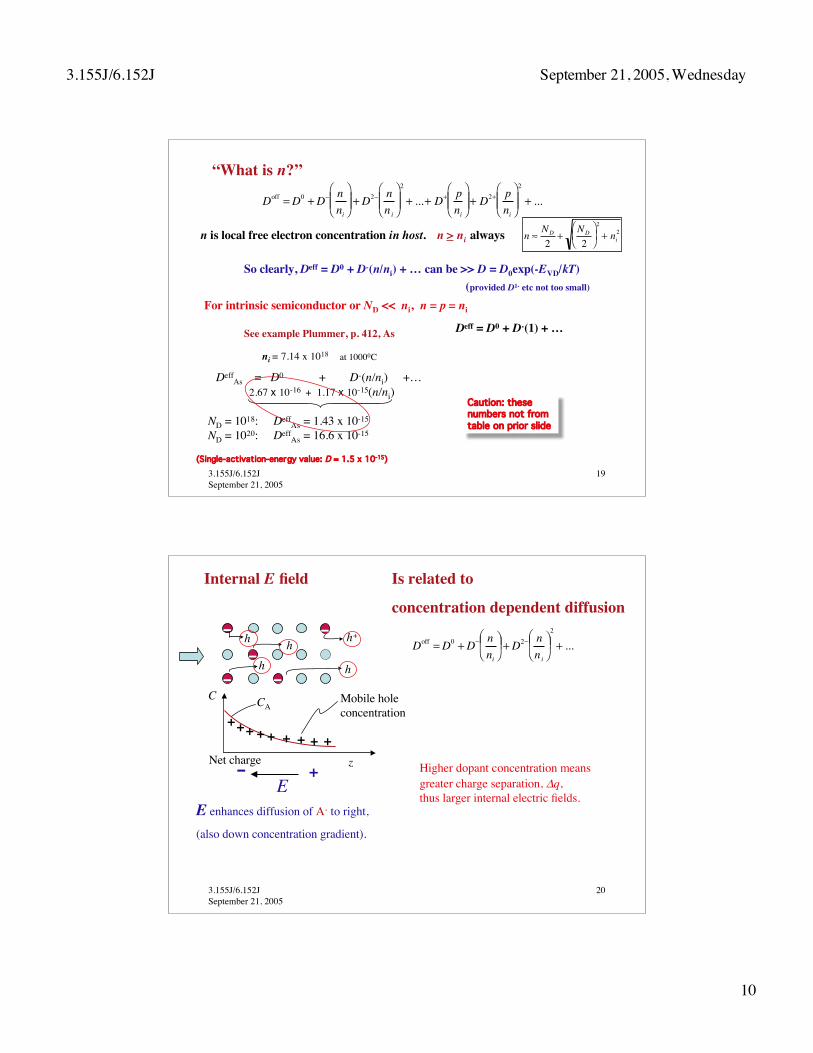
“What is n?”
n is local free electron concentration in host. n > ni always
So clearly, Deff = D0 + D-(n/ni) + … can be >> D = D0exp(-EVD/kT) (provided D1- etc not too small)
For intrinsic semiconductor or ND << ni, n = p = ni
Deff = D0 + D-(1) + …
DeffAs = D0 + D-(n/ni) +…
2.67 x 10⁻¹⁶ + 1.17 x 10⁻¹⁵(n/ni)
ND = 1018: DeffAs = 1.43 x 10⁻¹⁵
ND = 1020: DeffAs = 16.6 x 10⁻¹⁵
See example Plummer, p. 412, As
at 10000Cni = 7.14 x 10¹⁸
(Single-activation-energy value: D = 1.5 x 10⁻¹⁵)
Caution: thesenumbers not fromtable on prior slide
n !N
D
2+
ND
2
"
# $
%
& '
2
+ ni
2
3.155J/6.152JSeptember 21, 2005
20
+++ + + + + + +z
C CAMobile holeconcentration
Net charge- +E
E enhances diffusion of A- to right,
(also down concentration gradient).
Internal E field
− −
−
− −
h hh h
h+
Higher dopant concentration meansgreater charge separation, Δq,thus larger internal electric fields.
Doff
= D0
+ D! n
ni
"
#
$ %
&
' + D2! n
ni
"
#
$ %
&
'
2
+ ...
Is related to
concentration dependent diffusion

3.155J/6.152J September 21, 2005, Wednesday
11
3.155J/6.152JSeptember 21, 2005
21
ExerciseCalculate diffusivity of P in Si at 1000° C for a) cP < ni b) cP = 4 × 1019 cm-3
c) compare diffusion length b) with uncharged estimate
a) cP < ni = 1019
from Fig 1.16
3.155J/6.152JSeptember 21, 2005
22
ExerciseCalculate diffusivity of P in Si at 1000° C for a) cP < ni b) cP = 4 × 1019 cm-3
c) compare diffusion length b) with uncharged estimate
a) cP < ni = 1019
DP
!= 4.4exp !
4
kT
"
#
$
% = 6.63&10!16(cm2
s!1)
D = DP
0+ D
P
! n
ni
"
#
$ %
&
' =1.37 (10!14(cm2s!1)
Diffusion of P in Si D0 Ea D0
- Ea-
(cm2/s) (eV) (cm2/s) (eV)
3.85 3.66 4.4 4.0
Better than single-activation-energy :
DP
= 4.7exp !3.68
kT
"
# $
%
& ' =1.3(10
!14 (cm2s!1)
10
8nni 6
4
2
0 2 4 6 8 10ND/ni
n !N
D
2+
ND
2
"
# $
%
& '
2
+ ni
2
Plummer, Eq. 1.16
Linear approximation
Single-valued D
DP
0= 3.85exp !
3.66
kT
"
# $
%
& ' =1.3(10
!14 (cm2s!1)
Figure 1.16 in Plummer et al., 2000.
Figure removed for copyright reasons.
Please see:
3.155J/6.152J September 21, 2005, Wednesday
12
3.155J/6.152JSeptember 21, 2005
23
D = DP
0+ D
P
! n
ni
"
#$%
&'= 1.3(10!14
+ 6.63(10!16 4.24
1
"#$
%&'= 1.57 (10!14
(cm2s!1) vs 1.37
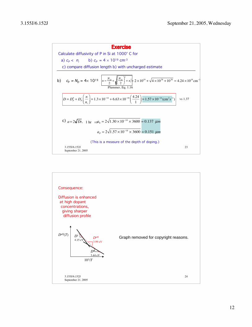
ExerciseCalculate diffusivity of P in Si at 1000° C for a) cP < ni b) cP = 4 × 1019 cm-3
c) compare diffusion length b) with uncharged estimate
b) cP = ND = 4× 10¹⁹
n !N
D
2+
ND
2
"
# $
%
& '
2
+ ni
2
= 2 !1019+ 4 !10
38+10
38= 4.24 !10
19cm
"3
a = 2 Dt, a0= 2 1.30 !10
"14! 3600 = 0.137 µm1 hr ⇒c)
aP= 2 1.57 !10
"14! 3600 = 0.151 µm
Plummer, Eq. 1.16
(This is a measure of the depth of doping.)
3.155J/6.152JSeptember 21, 2005
24
Consequence:
Diffusion is enhanced at high dopant concentrations, giving sharper diffusion profile
D1
4.15 eV
103/T
Deff(T)
D0
3.44 eV
Deff
3.99 eVGraph removed for copyright reasons.
3.155J/6.152J September 21, 2005, Wednesday
13
3.155J/6.152JSeptember 21, 2005
25
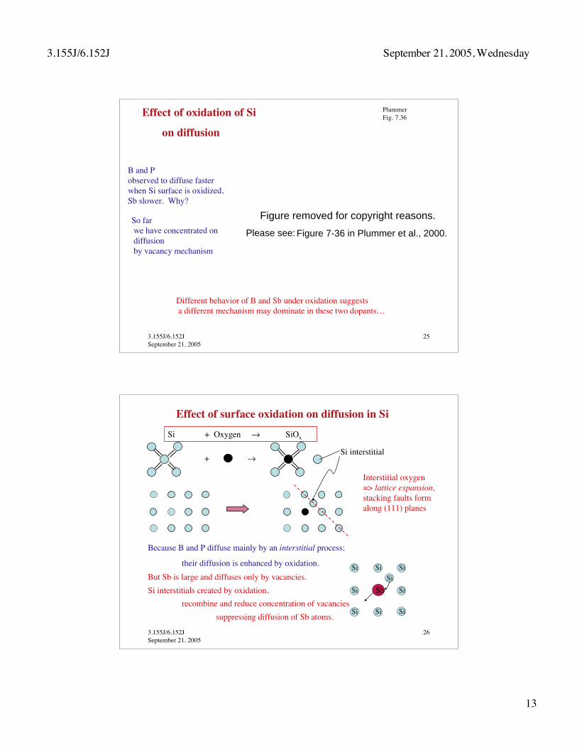
Effect of oxidation of Si
on diffusion
PlummerFig. 7.36
B and P observed to diffuse faster when Si surface is oxidized,Sb slower. Why?
Different behavior of B and Sb under oxidation suggests a different mechanism may dominate in these two dopants…
So far we have concentrated on diffusion by vacancy mechanism
3.155J/6.152JSeptember 21, 2005
26
Effect of surface oxidation on diffusion in SiSi + Oxygen → SiOx
+ →Si interstitial
Because B and P diffuse mainly by an interstitial process;
their diffusion is enhanced by oxidation.But Sb is large and diffuses only by vacancies.Si interstitials created by oxidation,
recombine and reduce concentration of vacanciessuppressing diffusion of Sb atoms.
Sb
SiSi
SiSi
Si
Si
Si
SiSi
Interstitial oxygen=> lattice expansion,stacking faults formalong (111) planes
Figure 7-36 in Plummer et al., 2000.
Figure removed for copyright reasons.Please see:
3.155J/6.152J September 21, 2005, Wednesday
14
3.155J/6.152JSeptember 21, 2005
27
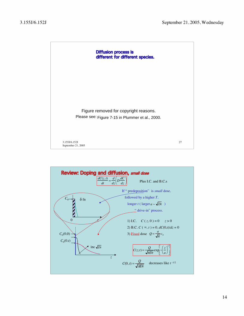
Diffusion process is different for different species.
3.155J/6.152JSeptember 21, 2005
28
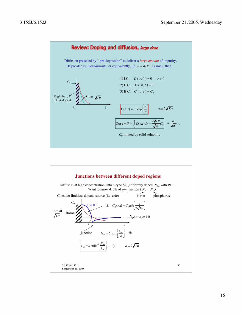
Review: Doping and diffusion, small dose
δ fnC0
0 z
If “ predeposition” is small dose,
followed by a higher T,
longer t ( larger )
“ drive-in” process.
a ~ Dt
C(z,t) =Q
!Dtexp "
z
a
#
$
%
&
2'
( )
*
+ ,
C(0, t) =Q
!Dtdecreases like t -1/2
1) I.C. C ( z, 0 ) = 0 z > 0
2) B.C. C ( ∞, t ) = 0, dC(0,t)/dz = 0
3) Fixed dose
Q =a
!c0
z
inc
Dt
C0(0,0)
C0(0,t)
dC(z, t)
dt=d
dzDdC
dz
!
"
#
$ Plus I.C. and B.C.s
Figure 7-15 in Plummer et al., 2000.Figure removed for copyright reasons.
Please see:
3.155J/6.152J September 21, 2005, Wednesday
15
3.155J/6.152JSeptember 21, 2005
29
Diffusion preceded by “ pre-deposition” to deliver a large amount of impurity. If pre-dep is inexhaustible or equivalently, if is small, then
a ~ Dt
C(z,t) = C0erfc
z
a
!
"
#
$
a = 2 Dt
Dose !Q = C(z,t)dz =2 Dt
"0
#
$ C0
=a
!C0
C0 limited by solid solubility
Review: Doping and diffusion, large dose
1) I.C. C ( z, 0 ) = 0 z > 0
2) B.C. C ( ∞, t ) = 0
3) B.C. C ( 0, t ) = C0Might beSiO2+ dopant
inc
Dt
C0
0 z
3.155J/6.152JSeptember 21, 2005
30
Junctions between different doped regionsDiffuse B at high concentration, into n-type Si, (uniformly doped, ND, with P).
Want to know depth of p-n junction ( NA = ND)
boron phosphorus
ND
= C0erfczjct
a
!
" #
$
% & junction
zjct = a erfc-1 ND
C0
!
" #
$
% &
a = 2 Dt
Consider limitless dopant source (i.e. erfc)
Small
Dt
CBz, t( ) = C
0erfc
z
2 Dt
!
" # $
% &
Boron
C0
z
ND (n-type Si)
Log |C|
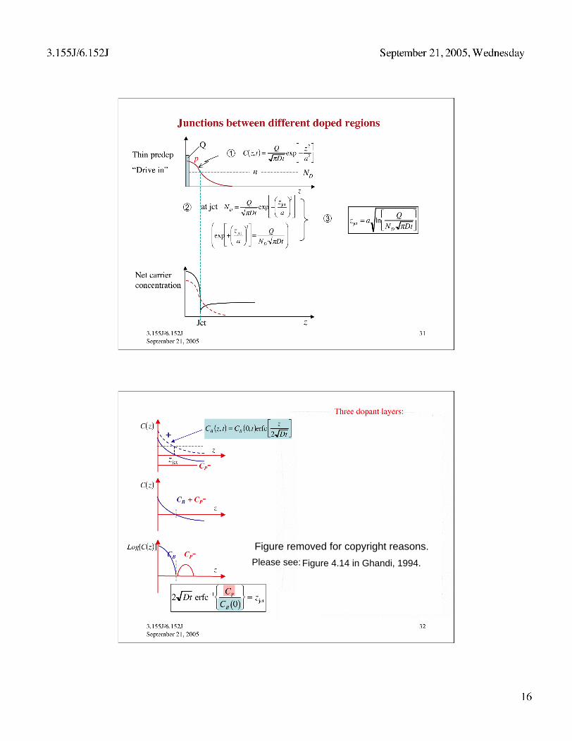
Figure 4.14 in Ghandi, 1994.
Figure removed for copyright reasons.Please see:

3.155J/6.152J September 21, 2005, Wednesday
17
3.155J/6.152JSeptember 21, 2005
33
Internal E fields alter Fick’s LawD is not a constant, but depends on c(x)
3.155J/6.152JSeptember 21, 2005
34
n-type Si, ND = 1016 cm-3 is doped with boron
from a const source with C0 (boron) = 1018 cm -3
Question:
If exposed to c0 at 1000°C for 1 hr,
what is junction depth?
From appendix, x = 1.82 = z/[2(Dt)1/2 ]
D boron( ) = 0.037exp !3.46
kT
"
# $
%
& ' 7.6 × 10⁻¹⁶ cm2/s1273 K
a = 2 Dt = 3.31!10"6cm = 0.033µm
zjct = 0.033!1.82 = 0.06µm
Exercise
ND = 1016 cm-3
C z,t( ) = C0erfc
z
a
!
"
#
$ ,
C0(boron)1018/cm3
zjct = a erfc-1 ND
C0
!
" #
$
% &
= 2 Dt erfc-110
'2[ ]
Let erfc-1 [10-2] = x , erfc[x] = 0.01 = 1-erf[x], erf [x] = 0.99
Figure 7-26 in Plummer et al., 2000.
Figure removed for copyright reasons.
Please see:

3.155J/6.152J September 21, 2005, Wednesday
18
3.155J/6.152JSeptember 21, 2005
35
Q = C z,1hr( )! dz =aC
0
"=1.87 #1012cm-2
7.57 !10"15cm
2
sD (boron)
1373 K
Dt = 5.22 !10"6cm
zjct = 0.033!1.82 = 0.06µm
From zjct(t) and zjct(0) = 0, you can calculate junction depth at different time:
z jct
1 hr t
zjct = 2 Dt erfc-110
!2[ ]
Question: Now constant source is removed
and this dose,C(z, 1hr) , is “ driven in”farther for 1 hr at 1100°C.
Now where is junction?
zjct = a lnQ
ND
!Dt
"
# $ %
& ' =1.8 (10)5cm = 0.18µm
3.155J/6.152JSeptember 21, 2005
36
Measuring diffusion profiles
R = !L
A("),
! =1
"= nqµ
! =RA
L("m)
But n, µ are functions of position due to doping
! =q
tn z( )
0
t
" µ n( )dz
! =1
"=
t
q nµdz#Define
sheet resistance
!
t" Rs =
RA
Lt= R
W
L(#
sq) an average measurement of n
AtI
L
Resistance resistivity conductivity
+ _
φ
Spreading resistance probe:(Developed at Bell Labs in ‘40s)

3.155J/6.152J September 21, 2005, Wednesday
19
3.155J/6.152JSeptember 21, 2005
37
4-point probe
I
V
Equipotentials
These � average n if done from surface.
These are most useful if done on beveled wafer: sample
Polish off � depth profile
Measuring diffusion profiles
Also square array
(Van der Pauw method)
I
V
�25 micronspacing
3.155J/6.152JSeptember 21, 2005
38
Hall effect: electrical transport in magnetic field.
F = q v � B
J = nq v
B I
V
++
++
___
__ e-
e-v
e-
e-
I
Again an average measurement
I
I
+
+
+ –
––
h+
h+v
V
B
F
q= EH =
J
nqB EH = RH J � B( )
RH =1
nqHall coefficient => charge signand concentrationRH is slope of V vs B data
B
VHLarge holeConcentration p
Small electronconcentration n
3.155J/6.152J September 21, 2005, Wednesday
20
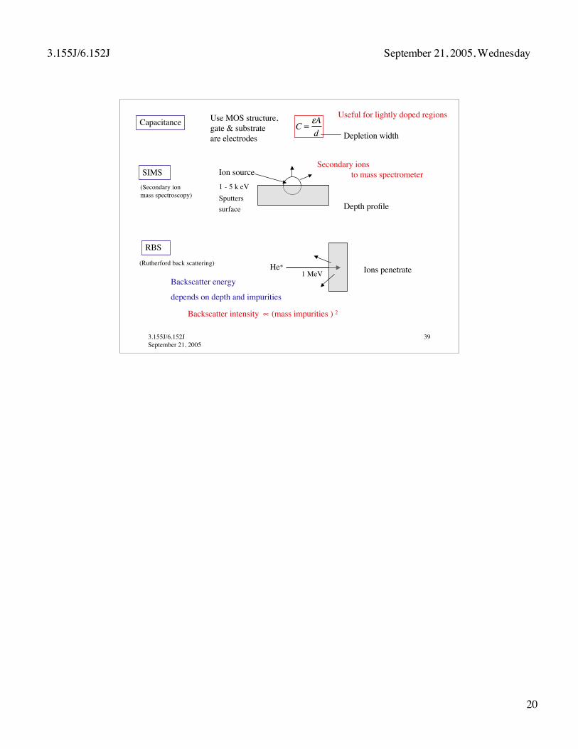
3.155J/6.152JSeptember 21, 2005
39
C =!A
d Depletion widthCapacitance
Useful for lightly doped regionsUse MOS structure, gate & substrate are electrodes
SIMS
Depth profile
Ion source1 - 5 k eVSputterssurface
Secondary ionsto mass spectrometer
(Secondary ionmass spectroscopy)
RBS
Ions penetrate
Backscatter intensity ∝ (mass impurities ) 2
Backscatter energy
depends on depth and impurities
He+1 MeV
(Rutherford back scattering)
Related Documents


![WORLD ANTI-DOPING AGENCY and THE ANTI-DOPING ORGANIZATION · world anti-doping agency and the anti-doping organization [insert name] _____ agreement governing the use and sharing](https://static.cupdf.com/doc/110x72/5c1bae9309d3f2826b8b8c64/world-anti-doping-agency-and-the-anti-doping-organization-world-anti-doping.jpg)