ECE-305: Spring 2016 MOS Band Bending Professor Mark Lundstrom Electrical and Computer Engineering Purdue University, West Lafayette, IN USA [email protected] 3/29/16 Pierret, Semiconductor Device Fundamentals (SDF) pp. 567-575

Welcome message from author
This document is posted to help you gain knowledge. Please leave a comment to let me know what you think about it! Share it to your friends and learn new things together.
Transcript
Lundstrom ECE 305 F16
ECE-305: Spring 2016
MOS Band Bending
Professor Mark Lundstrom Electrical and Computer Engineering
Purdue University, West Lafayette, IN USA [email protected]
3/29/16
Pierret, Semiconductor Device Fundamentals (SDF) pp. 567-575
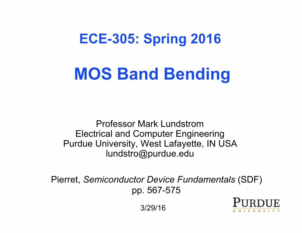
MOS capacitor
2
VG
p-Si
metal or
heavily doped “polysilicon”
SiO2
tox ≈ 1− 2 nm
Lundstrom ECE 305 F16
What happens as we sweep the gate voltage from negative to positive?

band banding in an MOS device
3 Fig. 16.6, Semiconductor Device Fundamentals, R.F. Pierret Flat band Accumulation Depletion Inversion
′VG = 0 ′VG < 0 0 < ′VG <VT ′VG > ′VT
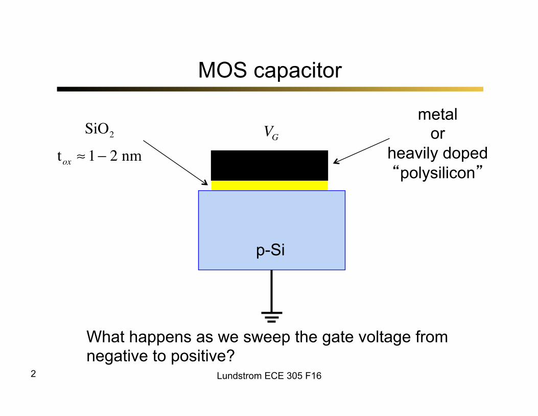
MOS capacitor (flatband)
4
′VG = 0
p-Si
ρ = 0 p0 = NA−
No metal-semiconductor workfunction difference
′VG = 0

MOS capacitor (accumulation)
5
′VG < 0
p-Si
ρ > 0 p0 > NA−
′VG < 0
Lundstrom ECE 305 F16

MOS capacitor (depletion)
6
′VG > 0
p-Si
ρ ≈ −qNA p0 << NA−
W
0 < ′VG < ′VT
Lundstrom ECE 305 F16
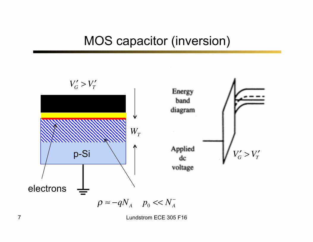
MOS capacitor (inversion)
7
′VG > ′VT
p-Si
ρ ≈ −qNA p0 << NA−
WT
electrons
′VG > ′VT
Lundstrom ECE 305 F16

band banding in an MOS device
8 Fig. 16.6, Semiconductor Device Fundamentals, R.F. Pierret Flat band Accumulation Depletion Inversion
′VG = 0 ′VG < 0 0 < ′VG <VT ′VG > ′VT
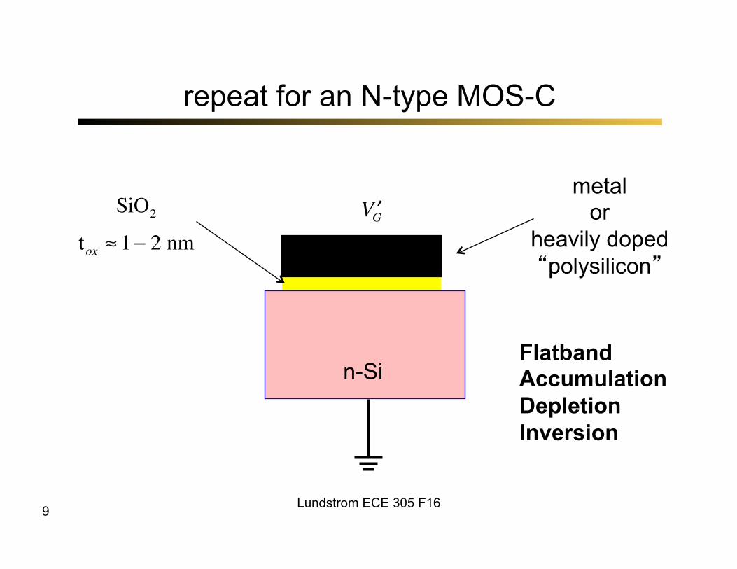
repeat for an N-type MOS-C
9
′VG
n-Si
metal or
heavily doped “polysilicon”
SiO2
tox ≈ 1− 2 nm
Lundstrom ECE 305 F16
Flatband Accumulation Depletion Inversion

hole density in the bulk
10
EC
EV
Ei
EF
Si
qφ x( ) φ = 0
W
x
qφF
φF =kBTqln NA
ni
⎛⎝⎜
⎞⎠⎟
φS
depletion:
pbulk = NA = nieEi bulk( )−EF( ) kBT
pbulk = NA = nieqφF kBT
Lundstrom ECE 305 F16
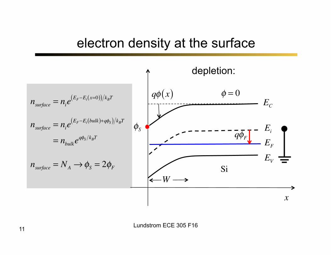
electron density at the surface
11
EC
EV
Ei
EF
Si
qφ x( ) φ = 0
W
x
qφF
nsurface = NA →φS = 2φF
φS
depletion:
nsurface = nieEF−Ei x=0( )( ) kBT
nsurface = nieEF−Ei bulk( )+qφS( ) kBT
= nbulkeqφS kBT
Lundstrom ECE 305 F16

onset of inversion
12
EC
EV
Ei
EF
Si
qφ x( ) φ = 0
W
x
qφF
φS = 2φF
depletion:
φF =kBTqln NA
ni
⎛⎝⎜
⎞⎠⎟
Lundstrom ECE 305 F16
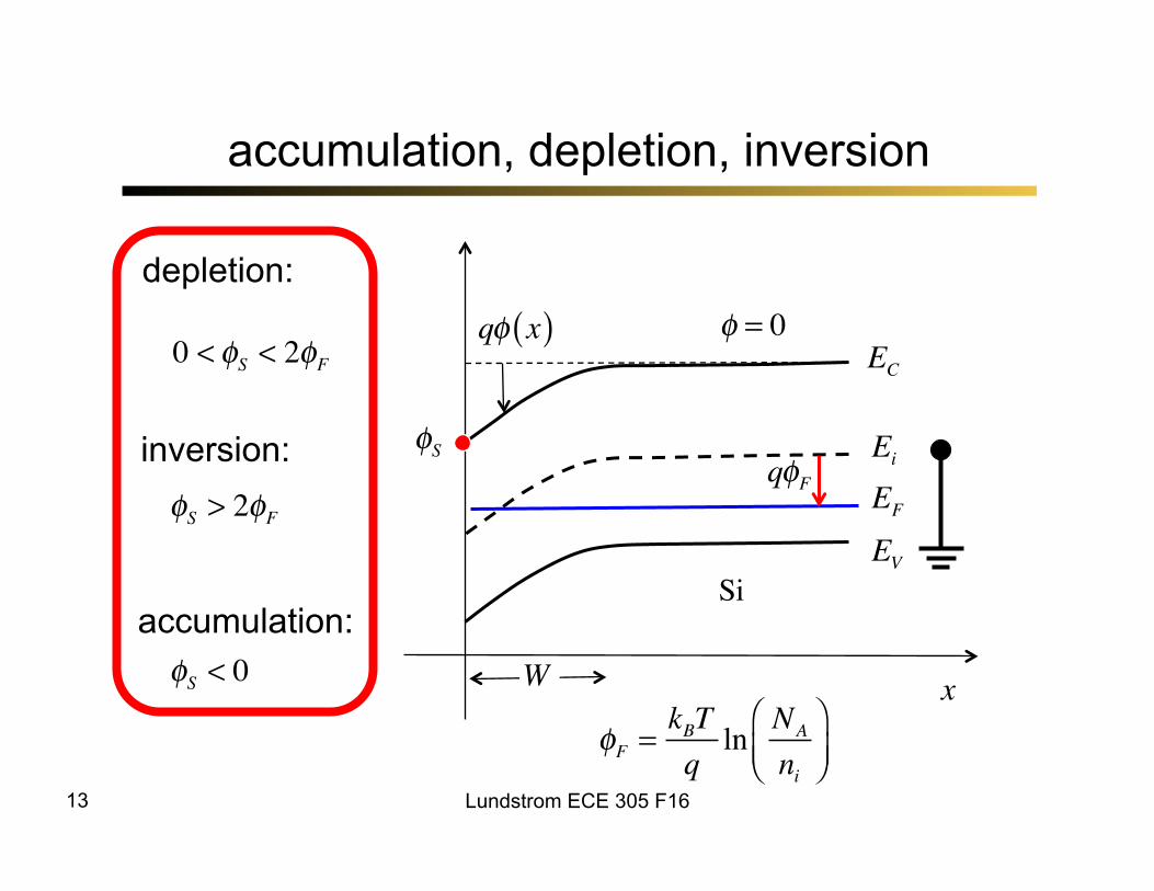
accumulation, depletion, inversion
13
EC
EV
Ei
EF
Si
qφ x( ) φ = 0
W x
qφF
φF =kBTqln NA
ni
⎛⎝⎜
⎞⎠⎟
φS
φS < 0
0 < φS < 2φF
φS > 2φF
accumulation:
depletion:
inversion:
Lundstrom ECE 305 F16
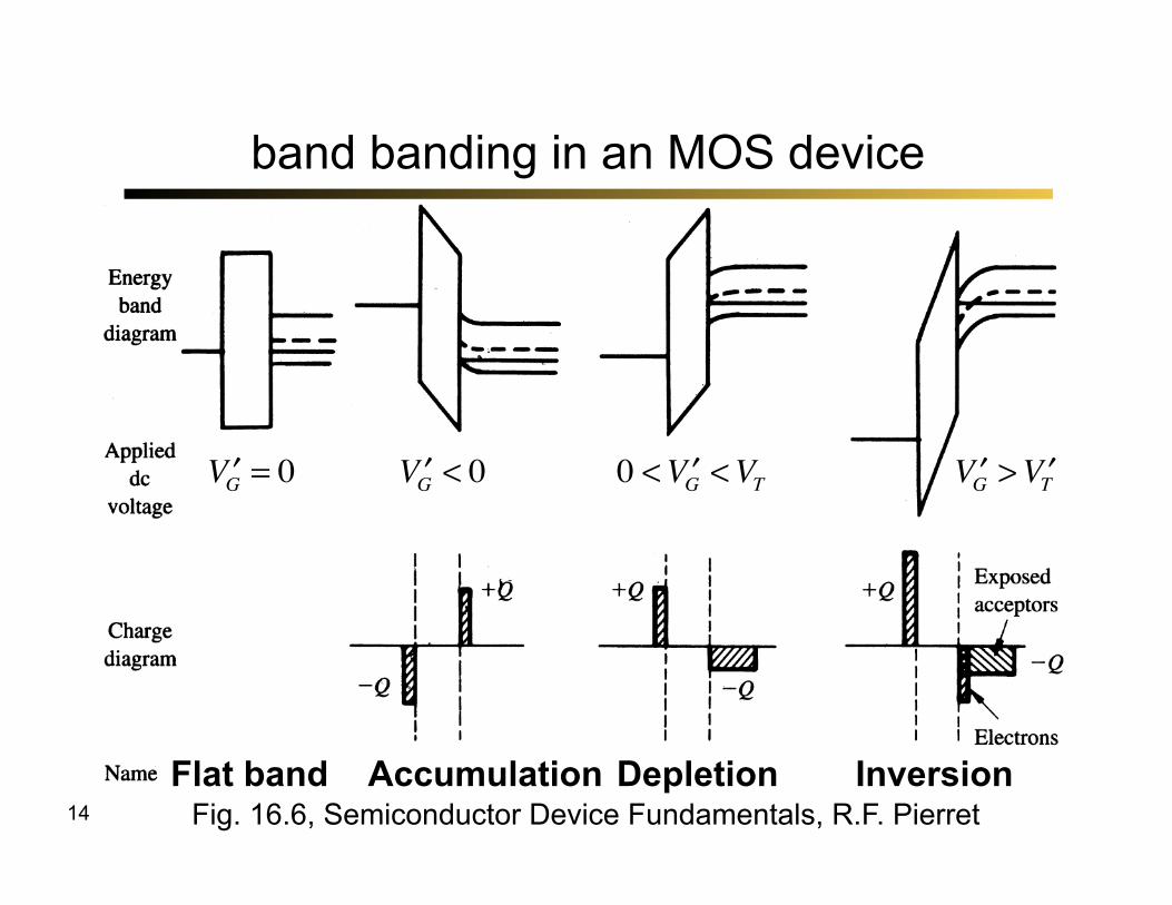
band banding in an MOS device
14 Fig. 16.6, Semiconductor Device Fundamentals, R.F. Pierret Flat band Accumulation Depletion Inversion
′VG = 0 ′VG < 0 0 < ′VG <VT ′VG > ′VT
Related Documents