Simulation Methodology Chapter 3 47 3 Simulation Methodology This chapter discusses the simulation methodologies which have been adopted during the course of this research programme. The first section discusses the principal concepts and the overall structure of the integrated atomistic process and device simulation strategy implemented with Technology Computer Aided Design (TCAD) device modelling tools. Detailed descriptions of the models involved in the process simulation of device fabrication sequences; including ion implantation, deposition, etching, diffusion and oxidation is the subject of the second section. The last section in this chapter provides an overview of device simulation methodology, by reviewing some of the physical models and simulation approaches used in this work. All the simulation techniques discussed in the three sections of this chapter have been calibrated and validated against real 35nm physical gate length MOSFETs fabricated and reported by Toshiba [3.1]. They have been used subsequently to scale the transistors according to the requirements of the ITRS (2003 edition) and to study the impact of intrinsic parameter fluctuations on such scaled devices. 3.1 TCAD and Integrated process & device simulation The state of the art in modelling and simulation covers a wide range of specialist areas related to the entire process of integrated semiconductor device manufacturing. The following are some of the main areas of modelling and simulation [3.2] typically covered by state of the art TCAD simulation tools:

Welcome message from author
This document is posted to help you gain knowledge. Please leave a comment to let me know what you think about it! Share it to your friends and learn new things together.
Transcript
Simulation Methodology Chapter 3
47
3
Simulation Methodology
This chapter discusses the simulation methodologies which have been adopted
during the course of this research programme. The first section discusses the principal
concepts and the overall structure of the integrated atomistic process and device
simulation strategy implemented with Technology Computer Aided Design (TCAD)
device modelling tools.
Detailed descriptions of the models involved in the process simulation of device
fabrication sequences; including ion implantation, deposition, etching, diffusion and
oxidation is the subject of the second section. The last section in this chapter provides
an overview of device simulation methodology, by reviewing some of the physical
models and simulation approaches used in this work.
All the simulation techniques discussed in the three sections of this chapter have
been calibrated and validated against real 35nm physical gate length MOSFETs
fabricated and reported by Toshiba [3.1]. They have been used subsequently to scale the
transistors according to the requirements of the ITRS (2003 edition) and to study the
impact of intrinsic parameter fluctuations on such scaled devices.
3.1 TCAD and Integrated process & device simulation
The state of the art in modelling and simulation covers a wide range of specialist areas
related to the entire process of integrated semiconductor device manufacturing. The
following are some of the main areas of modelling and simulation [3.2] typically
covered by state of the art TCAD simulation tools:
Simulation Methodology Chapter 3
48
• Front-end process modelling that characterizes the essential steps for device
manufacturing,
• Device modelling and simulation in order to understand how the devices operate
by studying their electrical characteristics and intrinsic physical properties,
• Compact modelling to perform circuit level device simulation
• Circuit modelling which simulates the behaviour of the integrated circuit as a
module,
• Modelling of equipment to study the general features of the deposition, etching
and other manufacturing processes.
However, a detailed discussion of all these physical models and simulation
methodologies is not the aim of this section. Therefore, the emphasis has been limited to
cover only the front end process and device modelling related to the aim and objectives
of this thesis.
3.1.1 The role of TCAD in advanced device design an d characterisation
As the processing power of computer technology doubles roughly every two
years, according to Moore’s law [3.3], the requirements of TCAD for advanced device
modelling, simulation and design expands considerably. TCAD is the synthesis of
process, device and circuit simulations using state of the art computer technology. One
of the most important advantages of using TCAD simulation and modelling is to
produce deep insight and understanding of the physical process involved in the
operation of the modern semiconductor devices.
Another dimension of the importance of TCAD in industry and research
environments is its role in reducing the time required for the development of new
generations of devices. This has an enormous implication on the over-all cost associated
with scaling and new product development. With the present day’s availability of
supercomputer technology it is possible to have a virtual simulation laboratory that is
capable of predicting the behaviour of new devices, and their electrical parameters,
resulting from a particular fabrication sequence with a reasonable degree of accuracy
[3.4]. This capability permits the design of an optimized prototype device and
technology in a relatively short period of time and with reduced development cost.
Simulation Methodology Chapter 3
49
In addition, TCAD modelling and simulation is also a vital tool in failure
analysis, trouble-shooting and inverse modelling. By incorporating statistical functions
into the TCAD package, it is possible to perform failure analysis and reliability tests. In
the inverse modelling process, the initial point is a device with a poorly-defined
structure, but known electrical parameters.
Using device simulation and calibration, one can deduce the realistic device
structure so that it can be used for further development purposes or scaling studies. This
will also be an important tool in the investigation of new materials and their impact on
device performance. Using simulation tools, one can perform not only a preliminary
analysis on the new material’s (for example high-κ dielectrics), reproducibility,
reliability and interface properties, but could also study their impact on the behaviour of
the new device.
The ever decreasing dimensions of CMOS devices, (now down to the sub
100nm technology nodes) together with the ever increasing complexity of
manufacturing technology [3.5] highlight the necessity of process and device simulation
more than ever. Technologically demanding and financially costly experimental
procedures can now be modelled and thoroughly analysed in a relatively short time
period.
All the benefits mentioned above emphasise the importance of TCAD
simulation as a tool in the field of device research and development. Despite all the
advantages in the development of new generation devices, TCAD has its own
drawbacks. There is always some degree of a mismatch between the measured data and
the simulated values. It is also possible to obtain completely misleading results from
device or process simulations.
The reasons could be the use of unphysical models, inappropriate simulation
techniques, and inaccurate default material and transport parameters. Moreover, most
simulation models are to some degree empirical, and require numerical calibration to
experimental data at each technology node. This means that simulation accuracy cannot
automatically be extended to the next generation of devices and technology nodes. This
is particularly true for the present generation of sub-100 nm devices where the short
channel effect, non-equilibrium transport, and quantum mechanics govern their
operation.
It is also very important to underline that computer simulation is not the final
word in overcoming the challenges in developing present and future technology

Simulation Methodology Chapter 3
50
generations. It can only be used as a probing instrument and predictive tool that
facilitates the environment for advanced MOSFET design and fabrication. Definite
analysis and conclusions still require confirmation, obtained from experimental results.
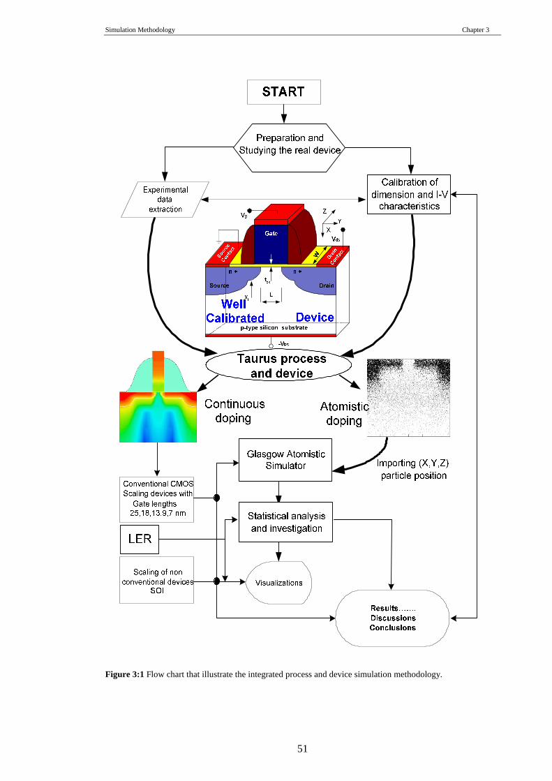
3.1.2 Integrated process and device simulation in 3 D
The underlying philosophy behind the integrated process and device simulation
of decanano-meter MOSFETs [3.6] is the systematic and methodological selection and
linking of various types of semiconductor TCAD tools efficiently. It is a “divide and
conquer” strategic approach which applies the best available models and tools for
designing and understanding scaled devices of succeeding generations of semiconductor
technology.
One of the main aims of this PhD work is to study the impact of different
sources of intrinsic parameter fluctuations on “real devices” created by the simulation of
a realistic process sequence. The nature of the fabrications requires a complete 3D
process and device simulation and is an example of the most demanding application of
TCAD tools.
In order to make 3D process model as realistic as possible, a well behaved 35
nm physical gate length MOSFET reported by Toshiba [3.1] has been adopted as a
bench mark device for this work. Here we will use the simulation of this device as an
example of the 3D integrated device simulation approach. Initially, comprehensive 3D
process simulation of the 35 nm device based on the real device fabrication sequence
was carried out with the 3D process simulator, Taurus, in order to deduce the device
geometry and doping profile. This information was subsequently exported to the device
part of the simulator, which gives electrical characteristics. These were then compared
with the experimental data in order to adjust the transport parameters and validate the
simulators.
The overall methodology of integrated process and device simulation used in
this work is illustrated on figure 3:1. The scaling of the 35 nm MOSFETs to the smaller
dimensions which correspond to the future technology nodes was then performed using
a continuous doping Taurus process and device simulator. The impact of Line Edge
Roughness (LER) was also studied using continuous doping effects.
Simulation Methodology Chapter 3
51
Figure 3:1 Flow chart that illustrate the integrated process and device simulation methodology.
Simulation Methodology Chapter 3
52
In order to study more accurately the effect of discrete random dopants on the
critical device parameters, statistical process simulations were carried out based on the
well calibrated model by using the kinetic Monte Carlo process simulator, DADOS
[3.7][3.8].
The DADOS* atomistic diffusion simulator, which is incorporated into the
Taurus process simulator, provides the positions of the discrete dopants in the channel
source and drain regions. This extracted data was then imported into the Glasgow
Atomistic Device Simulator [3.9] to perform atomistic device simulations. Moreover,
(in chapter 5) the integrated device simulation methodology has been used to investigate
LER as one of the sources of intrinsic parameter fluctuations.
3.2 Front end Process Simulation – 3D
Process simulation deals with most of the technology steps involved in
semiconductor device fabrication. It enables engineers and technologists to predict the
most effective device structure, to optimize the critical device parameters and to perfect
the fabrication process flow environment and technology. It is also an instrumental tool
in the progression of successive generations of semiconductor technology and enhances
the research opportunities for creation of new non-classical device structures such as the
silicon on insulator structures and the multi gate devices [3.10].
Moreover, it sheds light on the effects of the actual fabrication processing on the
functionality and physical properties of resulting devices. Using the well calibrated
device structure obtained from process flow simulations, one can carry out device
simulations in order to analyze their electrical parameters (for example, threshold
voltage, and drive current and device behaviour). It is also possible to investigate the
possible performance and interactions when these devices are integrated in to a system.
To summarize, process simulation is important for modelling, design, prototype
evaluation, parameter optimization and at the same time enables the development of
new generations of devices and advanced integrated systems. Therefore, process
simulation has made an enormous contribution to the field of semiconductor process
integration.
* More discussions on DADOS is given in section 3.2.5
Simulation Methodology Chapter 3
53
As mentioned in the previous sections, the research presented in the thesis is
underpinned by data extracted from realistic MOSFETs. The calibration of the
simulation methodology in respect of these devices, which involves a painstaking
process simulation, is a vital ingredient of the overall simulation methodology. Taking
this into consideration, a step-by-step calibration strategy (described in detail in chapter
4) was employed to perform process and device simulations.
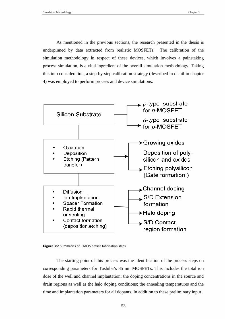
Figure 3:2 Summaries of CMOS device fabrication steps
The starting point of this process was the identification of the process steps on
corresponding parameters for Toshiba’s 35 nm MOSFETs. This includes the total ion
dose of the well and channel implantation; the doping concentrations in the source and
drain regions as well as the halo doping conditions; the annealing temperatures and the
time and implantation parameters for all dopants. In addition to these preliminary input
Simulation Methodology Chapter 3
54
data required to run process simulations, it is also equally important to extract the
device dimensions such as the gate length, oxide thickness, the source/drain shallow
junction depth and to define a computationally reasonable size of simulation domain.
Such extraction is mainly based on high resolution TEM images. Once the above
information has been obtained, ‘Taurus Process and Device’ simulation software [3.11]
was employed to perform a realistic device process flow simulation. Taurus Process and
Device simulation is a commercial TCAD tool enhanced by a 3D simulation capability
with a wide range of physical simulation model options.
In the course of this research project, the main fabrication processes steps
involved in the device process simulation sequences are: ion implantation, deposition,
etching, and diffusion as a result of rapid thermal annealing (RTA). The steps are
summarised in figure 3.2. Although this section does not attempt to give a
comprehensive review of these device fabrication steps, a general discussion of the
processes involved with the process flow steps included in the integrated device
simulation methodology will be presented in the following sections.
3.2.1 Implantation – The Introduction of impurities in to Si crystal
A pure, intrinsic silicon crystal has a poor electrical conduction due to a low
intrinsic carrier concentration (1.4×1010 cm-3) at 300K [3.12]. However, it is possible to
significantly change the local electrical conductivity or the conductivity type of the
silicon crystal by introducing a controlled amount of impurity atoms (dopants) [3.13].
Currently, there are two ways to achieve this: the first method is the diffusion of dopant
atoms from gaseous, liquid, or solid sources and the second is via ion implantation into
the host semiconductor. In order to be consistent with the Toshiba MOSFETs
fabrication sequence, this discussion concentrates on ion implantation.
The process of selectively incorporating extrinsic ions into semiconductor
materials through surface bombardment of high velocity (and energy) is known as ion
implantation [3.14]. It has been used for over two decades in silicon integrated process
technology.
Simulation Methodology Chapter 3
55
Ion implantation has several important advantages over the process of diffusion
of dopant atoms into semiconductors. One of the main advantages is that there is a great
deal of control over the amount of introduced impurities and over the impurity profile,
i.e. the ability to locate the impurities at the desired depth of the host semiconductor
[3.15] [3.16]. Another advantage is the possibility of using various types of ions which
are otherwise difficult to introduce by diffusion [3.17]. The capability of performing ion
implantation within a room temperature environment (reducing the effects of out-
diffusion and the undesirable spread of the intended profile) and in a relatively short
period of time is also another advantage.
Generally, elements in group III (old group nomenclature) (trivalent impurities)
and group V (pentavalent impurities) of the periodic table have been used as dopants in
silicon crystals by semiconductor manufacturers for decades. The chemical properties of
group-III elements initiate a p-type conductivity (generally known as acceptors) by
creating hole or electron deficiency. On the other hand group-V elements initiate n-type
conductivity (donors), by providing an extra electron. Accordingly, indium for the n-
MOSFET and arsenic for the p-MOSFET channel doping have been used to
manufacture the 35nm Toshiba MOSFETs, which are at the focus of this research.
Boron and (BF2) + are the most commonly used impurities in semiconductors in
the past as well as at the present time. Recently, however, indium is beginning to
replace these materials as recent research has shown that indium, due to its low
diffusion coefficient, is a good choice to form the super steep retrograde channel
(SSRC) doping profiles required beyond the 0.18µm technology node. The SSRC
doping profile can be achieved by using a heavy ion with shallow projected range of
distribution in the silicon crystal. Indium has properties that make it a good candidate to
form SSRC doping profile as has been shown in [3.18] [3.19] [3.20]. More discussion
on SSRC is given in section 2.2.3
There are three ion implantation models (Monte Carlo, Dual Pearson and
Gaussian) which are incorporated into the Taurus Process and Device simulation
software [3.11], to approximate the ion range distributions in the silicon substrate. This
work considers the Dual-Pearson distribution model during the process simulation.
However the Gaussian distribution has been used to specify an initial estimation of the
projection range (Rp) and the standard deviation, σ. These two models will be discussed
in section 3.2.3. No effort will be made to discuss the Monte Carlo implantation model
Simulation Methodology Chapter 3
56
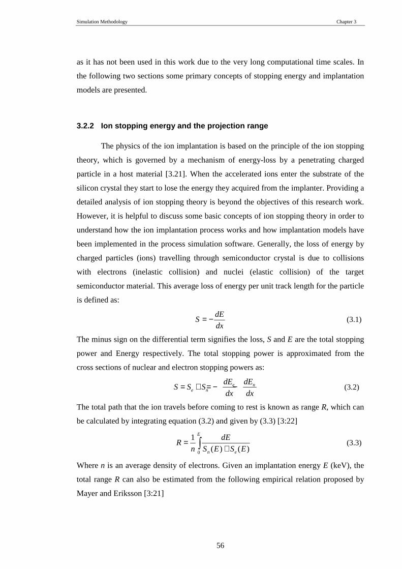
as it has not been used in this work due to the very long computational time scales. In
the following two sections some primary concepts of stopping energy and implantation
models are presented.
3.2.2 Ion stopping energy and the projection range The physics of the ion implantation is based on the principle of the ion stopping
theory, which is governed by a mechanism of energy-loss by a penetrating charged
particle in a host material [3.21]. When the accelerated ions enter the substrate of the
silicon crystal they start to lose the energy they acquired from the implanter. Providing a
detailed analysis of ion stopping theory is beyond the objectives of this research work.
However, it is helpful to discuss some basic concepts of ion stopping theory in order to
understand how the ion implantation process works and how implantation models have
been implemented in the process simulation software. Generally, the loss of energy by
charged particles (ions) travelling through semiconductor crystal is due to collisions
with electrons (inelastic collision) and nuclei (elastic collision) of the target
semiconductor material. This average loss of energy per unit track length for the particle
is defined as:
dx
dES −= (3.1)
The minus sign on the differential term signifies the loss, S and E are the total stopping
power and Energy respectively. The total stopping power is approximated from the
cross sections of nuclear and electron stopping powers as:
e ne n
dE dES S S
dx dx= + = − − (3.2)
The total path that the ion travels before coming to rest is known as range R, which can
be calculated by integrating equation (3.2) and given by (3.3) [3:22]
0
1
( ) ( )
E
n e
dER
n S E S E=
+∫ (3.3)
Where n is an average density of electrons. Given an implantation energy E (keV), the
total range R can also be estimated from the following empirical relation proposed by
Mayer and Eriksson [3:21]
Simulation Methodology Chapter 3
57
12 2 2
3 3
60 i ss i s
s i i
Z ZM M MER
g Z M Z
+ + =
(3.4)
where g is the density of the host semiconductor, Ms and Mi are the atomic mass of the
semiconductor material and the implanted atom, Zs and Zi are atomic numbers of the
semiconductor material and the implanted atoms respectively. The average depth, which
is the perpendicular distance from the crystal surface to the projection plane of the
implanted ions, is known as the projected range Rp. It is one of the important parameters
of ion implantation in semiconductor technology [3.21] [3.23]. The total path the ion
travels, R, could be shorter or longer than its projected range Rp. Using the results from
the empirical formula (3.4) the projection range Rp can be estimated from (3.5) and is
given by
1 3p
s i
RR
M M=
+ (3.5)
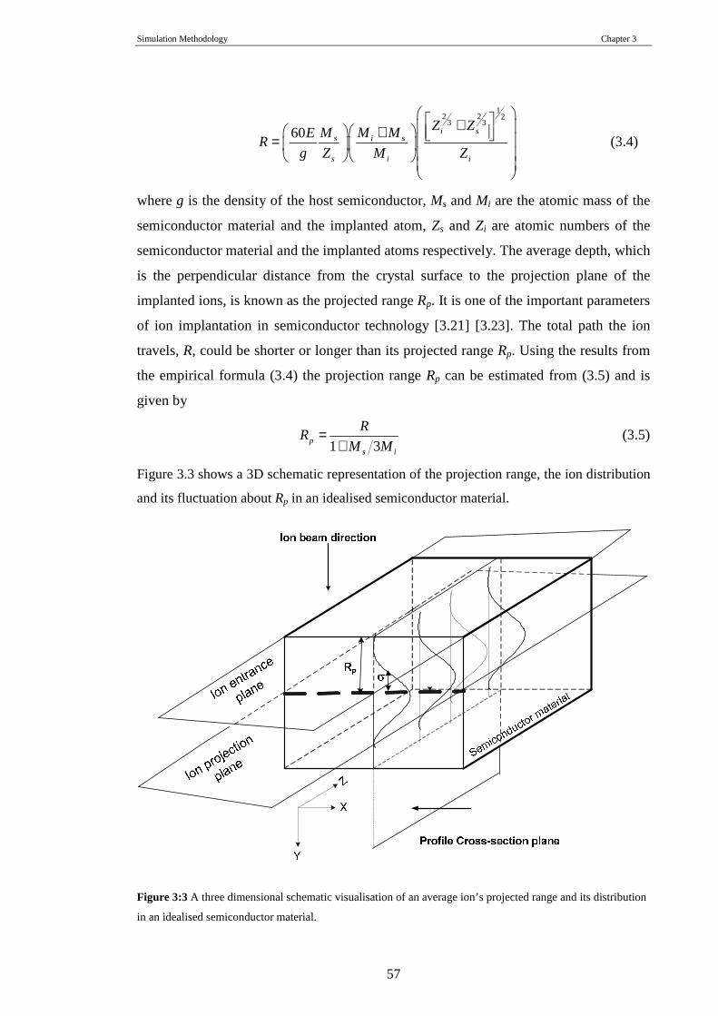
Figure 3.3 shows a 3D schematic representation of the projection range, the ion distribution
and its fluctuation about Rp in an idealised semiconductor material.
Figure 3:3 A three dimensional schematic visualisation of an average ion’s projected range and its distribution
in an idealised semiconductor material.

Simulation Methodology Chapter 3
58
The ion beam direction for the channel doping usually perpendicular to the
entrance plane. However, in some cases ion implantation may be performed with the
projection angle up to 30o off the vertical axis. The projection plane is where one
expects the maximum concentration of doped ions. For example in the case of our
reference (Toshiba) device, the halo doping implantation is performed with tilt angle of
30o off the perpendicular to the target plane. The vertical distance between the
projection plane and ion entrance plane is equivalent to the average projection distance,
Rp. By rotating the cross-section plane 90o about the Y-axis to bring it in parallel to X-Y
plane, the 1-D implanted ion (generally Gaussian) distribution profile could be seen
clearly. Statistically speaking, the range distribution is random event and it is expected
to have a profile close to a Gaussian distribution as depicted in figure 3.3 above.
3.2.3 The Gaussian and dual Pearson implantation mo dels
The realistic channel profile in the Toshiba MOSFETs has been approximated
by incorporating two virtual implantation stages in the Taurus process simulations
(described in chapter 4), from which the average depth of the implanted ions and their
distribution about the vertical depth have been extracted. Generally, according to the
LSS theory of the projected range, [3.22] the ion distribution within semiconductors and
in amorphous materials is assumed to be a near Gaussian distribution given by equation
(3.6) below. This is due to the statistical nature of ion stopping and scattering
mechanisms.
2( )1
( ) exp22
p
pp
x RN x
σπσ
−Φ = −
(3.6)
Here Φ is the ion flux, generally known as total ion dose of implantation per unit area
[ions/cm2]. It is the total number of ions per unit area enclosed by the Gaussian curve on
the projection plane.
If the maximum doping concentration is denoted by No [ions/cm3], it can be
directly obtained from equation (3.6) for px R= .
Simulation Methodology Chapter 3
59
0.4
2o
pp
Nσπσ
Φ Φ= ≅ (3.7)
The Gaussian distribution has been used for preliminary estimations of the two
statistical moments of ion distribution, namely the ion projected range and the standard
deviation about the mean. However, the Gaussian distribution is not a particularly good
model to approximate the ion implantation profile in sub-50 nanometre devices. Since
the main focus of this work deals with the scaling of nano-MOSFET devices right up to
the end of semiconductor technology roadmap’s prediction, it is a vital to implement the
correct implantation model that describes the doping profile of such devices more
accurately.
The Dual Person statistical model (courtesy of the applied mathematician and
statistician Karl Pearson) is a better description of the ion distribution as it includes the
ion channelling effect in the silicon lattice in contrast to the simpler Gaussian
distribution model, which is appropriate for another targets. Unlike the Gaussian
distribution, however, the Person IV family of distributions require the third and fourth
moments of the distribution in addition to the first and second moments. The first of
these extra moments is the skewness of the distribution, which indicates the degree of
departure from symmetry in the distribution. The second moment is kurtosis, which is
the measure of how sharp the peak (leptokurtic) is, or alternatively how flat (platykurtic)
the top of the distribution is. The measures of skewness and kurtosis have often been
taken relative to the normal distribution. In this work, the shape of the channel profile is
better described as leptokurtic rather than platykurtic (figure 4:6 in chapter 4).
Since the Pearson distribution family is a better approximation to the doping
distribution compared to the simple Gaussian mode, the Dual Person implantation
model has been adopted for device process simulation in this work. Therefore we, will
revisit some of the basic properties and equations of the dual Person statistical
distribution. The Person distribution is given by the solution of the following
differential equation: [3.24, 3.25, 3.26]
2
210
)()()(
xbxbb
xfax
dx
xdf
++−= (3.8)
Simulation Methodology Chapter 3
60
Where the coefficients (a, b0, b1, and b2) of the quadratic terms are constants that
can be described in terms of the four moments calculated from an arbitrary
experimentally obtained distribution ( )f x . The detailed solution and analysis of the
deferential equation of ( )f x (3.8) is given in references [3.24]. The first moment about
the origin is the mean value (which is equivalent to the average projection range Rp), is
given by (3.9)
∫∞
∞−Φ== dxxxfmRp )(
11 (3.9)
The peak value of the ion concentration (No) is at the position determined by the
projected range. The higher moments (m2, m3, and m4) are calculated about the first
moment using equation (3.9). For most impurities these parameters have been tabulated
as a function of implantation energies. The major early works on implantation by
Gibbons et al [23] were based on a Gaussian distribution and applied to amorphous
materials; it is not suitable for use in the implantation model adopted in this work.
Other work on ion projection statistics calculation was reported by Peterson and
Fichtner [27]. However, this work offers limited data for the indium impurity
distribution properties within the silicon crystal. Therefore, it is necessary to estimate
the Pearson distribution parameters for indium from the empirically calibrated equation
which will be discussed in the next section. For this purpose the set of equations (3.10-
3.11c) were used.
The general expression of the kth moment of the distribution about the average
projection range, Rp, is given by
( )∫∞
∞−
−Φ
= dxxfRxm kpk )(
1 (3.10)
From which the standard deviation, Skewness, and Kurtosis of the distribution may be
determined.
Standard deviation 2mp =σ (3.11a)
Skew 33
σγ m
= (3.11b)
Kurtosis 44
σβ m
= (3.11c)
The constants a, b0, b1, and b2 in equation (3.8) are, therefore, given in terms of the
distribution moments described in (3.11a, b, c) as follows.
Simulation Methodology Chapter 3
61
( )
181210
342
2
−−−
−=γβ
γβma (3.12a)
( )181210
32
20 −−
−−==
γββγm
ba (3.12b)
2
2
(2 3 6)
10 12 18c
β γβ γ
− −= −− −
(3.12c)
3.2.4 Diffusion
Diffusion, from a device’s fabrication point of view, accompanies every high
temperature process step. The initial application of diffusion was for introducing
dopants into a semiconductor material, changing the conductivity of a selected substrate
region of interest; the formation of source and drain region of MOSFETs prior to the
advent of implantation. The other process step that involves diffusion is the oxidation of
the silicon surface, leading to the formation of the Si/SiO2 interface [3.28]. This is
usually accompanied by segregation which affects the doping profile of the interface.
The diffusion process is also the responsible for doping redistribution during the post
implantation rapid thermal annealing needed for the electrical activation of implanted
ions [3.29].
As the energy of implantation and dose are vital parameters in the ion
implantation process, the diffusion time and the temperature are the two major
parameters governing the diffusion process [3.30]. Implantation of ions is usually done
at room temperature. By contrast, the diffusion of ions needs a high temperature in the
region of 800o-1200o centigrade [3.31] for silicon. In this work diffusion is mainly
associated with the annealing process step. For example, in the formation of very
narrow source and drain junction depths ( 20 xj nm≤ ), spike rapid thermal annealing
(RTA) and damage recovery annealing after high energy (100-240keV) well and
channel implantation were applied. In the final part of this section a brief overview of
the basic equations and major types of diffusion are presented. For further reading and
extensive discussions see the recommended references [3.29-3.30].
The diffusion equation used by the Taurus process simulator is based on Fick’s
law of solid-state diffusion given by
Simulation Methodology Chapter 3
62
NF D
x
∂= −∂
(3.13)
Where F is the diffusion flux defined as the rate of ion transfer per unit area, D and N
are diffusivity [cm2/sec] and ion concentration [atoms/cm3] respectively. The minus
sign signifies that the direction of the flux is opposite to the direction of the gradient.
Rearranging the terms, and considering the fact that the rate of change in concentration
with respect to time and the decrease in flux with respect to depth of diffusion are equal
(N F
t x
∂ ∂= −∂ ∂
), equation (3.13) can be generalised to give Fick’s second law of diffusion
given by:
2
2
( , ) ( , )N x t N x tD
t x
∂ ∂=∂ ∂
(3.14)
In order to solve equation (3.14) various diffusion conditions have been considered. For
example, concentration dependant diffusivity, constant diffusivity and temperature
dependant diffusivity have all been studied [3.29].
In most cases of the present fabrication technology of CMOS devices, diffusion
processes have been supplanted by ion implantation as the main method of impurity
introduction to the silicon crystal. The main reasons for this were discussed above
3.2.5 Diffusion and Defects, Object-oriented Simula tor (DADOS)
As CMOS devices are heading towards decananometer dimensions, variations in
dopant number and their position in the channel will make device parameters vary from
device to device. The threshold voltage and drive current variations are the most
important parameters affected by this phenomenon. Information on the microscopically
varying distribution of the dopants from realistic process simulation is vital in order to
perform statistical device simulation.
In a ‘standard’ statistical atomistic process simulation, a continuous doping
profile (obtained analytically or by using PED based process simulators) is used to
generate the random discrete dopant distribution in large samples of macroscopically
identical but microscopically different devices, using a variety of stochastic techniques
[3.32, 3.33 ]. In this work we explore the possibility of using DADOS [3.7] [3.34] as a
Simulation Methodology Chapter 3
63
direct source of stochastic discrete dopants distribution for statistical atomistic device
simulation. DADOS is an integrated part of the Taurus Process and Device simulator. It
is a 3D atomistic process simulator based on the kinetic Monte Carlo algorithm
designed to study the fundamental physical diffusion phenomena in silicon. It performs
atomistic level process simulation during the implantation and diffusion processes as
they happen, i.e., it simulates the sequence of happenings (like point defect and
emissions) at any given time and calculates ∆∆∆∆t between individual events. That means
the simulation time step is not constant [3.35].
DADOS’s integration to Taurus enables it to perform the complete atomistic
process simulation steps (for example: implantation, deposition, annealing, oxidation)
of realistic devices. Figure 3.4 depicts the 3D discrete doping profile of the 35 nm
device, from which the dopant positions are imported from DADOS simulation.
Figure 3:4 Discrete dopant distribution imported from DADOS in to the 35 nm test MOSFET. The solution
domain is 240×150×35 (in nm)
Simulation Methodology Chapter 3
64
3.2.6 Oxidation
The oxidation process is one of the most important steps in semiconductor
fabrication resulting in grow of insulators like silicon dioxide or silicon oxy-nitride.
Insulating layers are mainly used in CMOS devices for the purposes of surface
protection, passivation and as a gate insulator between the gate electrode and the silicon
substrate. Dielectrics may be grown using wet or dry oxidation in an oxygen rich
atmosphere or by the direct deposition method on the silicon substrate (chemical-vapour
deposition in the conditions of low or atmospheric pressure or plasma assisted). Figure
3.4 depicts the conventional oxidation process adopted in the standard Deal-Grove
model [3.36].
In Taurus, the simulation of the oxide growth is based on the Deal-Grove model.
The Deal-Grove model describes the different phases of the oxidation process which
take place during device fabrication as illustrated in figure 3.5.
Figure 3:5 Illustration of the oxidation process adapted from [3.36]
Simulation Methodology Chapter 3
65
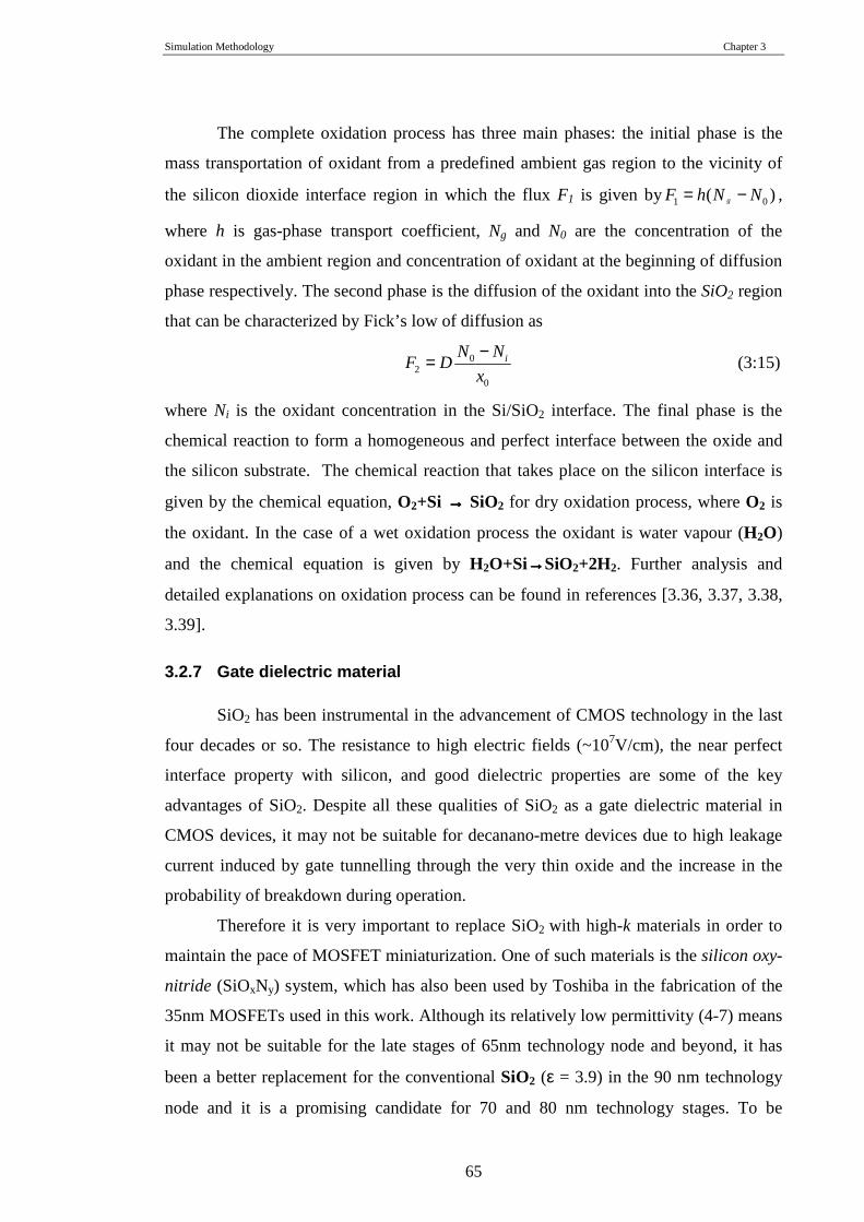
The complete oxidation process has three main phases: the initial phase is the
mass transportation of oxidant from a predefined ambient gas region to the vicinity of
the silicon dioxide interface region in which the flux F1 is given by 1 0( )gF h N N= − ,
where h is gas-phase transport coefficient, Ng and N0 are the concentration of the
oxidant in the ambient region and concentration of oxidant at the beginning of diffusion
phase respectively. The second phase is the diffusion of the oxidant into the SiO2 region
that can be characterized by Fick’s low of diffusion as
02
0
iN NF D
x
−= (3:15)
where Ni is the oxidant concentration in the Si/SiO2 interface. The final phase is the
chemical reaction to form a homogeneous and perfect interface between the oxide and
the silicon substrate. The chemical reaction that takes place on the silicon interface is
given by the chemical equation, O2+Si →→→→ SiO2 for dry oxidation process, where O2 is
the oxidant. In the case of a wet oxidation process the oxidant is water vapour (H2O)
and the chemical equation is given by H2O+Si→→→→SiO2+2H2. Further analysis and
detailed explanations on oxidation process can be found in references [3.36, 3.37, 3.38,
3.39].
3.2.7 Gate dielectric material
SiO2 has been instrumental in the advancement of CMOS technology in the last
four decades or so. The resistance to high electric fields (~107V/cm), the near perfect
interface property with silicon, and good dielectric properties are some of the key
advantages of SiO2. Despite all these qualities of SiO2 as a gate dielectric material in
CMOS devices, it may not be suitable for decanano-metre devices due to high leakage
current induced by gate tunnelling through the very thin oxide and the increase in the
probability of breakdown during operation.
Therefore it is very important to replace SiO2 with high-k materials in order to
maintain the pace of MOSFET miniaturization. One of such materials is the silicon oxy-
nitride (SiOxNy) system, which has also been used by Toshiba in the fabrication of the
35nm MOSFETs used in this work. Although its relatively low permittivity (4-7) means
it may not be suitable for the late stages of 65nm technology node and beyond, it has
been a better replacement for the conventional SiO2 (ε = 3.9) in the 90 nm technology
node and it is a promising candidate for 70 and 80 nm technology stages. To be
Simulation Methodology Chapter 3
66
consistent with fabrication process of the realistic Toshiba device, SiOxNy has been
adopted as the gate dielectric material rather than the conventional silicon dioxide for
this project.
In the case of the Toshiba device, the SiOxNy gate dielectric was grown by
performing an NO (for nitridation) gas annealing on very thin (1-1.2nm) base oxide
surface [3.1]. 2D growth of gate oxides of 1.2nm thickness in the process simulator is
computationally time consuming. Therefore, a deposition technique was used during the
device calibration process.
However, by doing this one neglects segregation and the effect of stress on the
process flow and eventually the likely effect of stress on the electrical characteristics of
the devices during the device simulation is nullified. It should be also noticed that the
permittivity of the resulting oxy-nitride system varies greatly with its stoichiometry. As
the exact composition of the oxy-nitride is unknown, it may only be approximated. The
approximation is given in section 4.
3.3 Device simulation
In order to understand the electrical properties of the modelled semiconductor
devices one has to perform device simulations. Device simulation provides a clear
understanding of general device operations, how the key parameters like threshold
voltage, subthreshold slope, off and on currents behave in relation to device dimensions,
and doping concentrations. It also provides microscopic information about potential
carrier concentrations, field, and current distribution within the device.
In this work, 2-D and 3-D device simulations techniques have been adapted in the
process of calibration, scaling and the investigation of intrinsic parameter fluctuations in
MOSFETs. In this section the basic governing equations are reviewed. A brief
comparison of different approaches to device simulation and concise overview of
physical models used in this work are presented.
3.3.1 Equations governing device operation
In the drift diffusion approximation, operation of semiconductor devices including
MOSFETs can be described by using three main equations solved self consistently,
which are the building blocks of computer aided device simulation tools. One of these
fundamental equations is the classical Poisson equation that describes the electrostatic
Simulation Methodology Chapter 3
67
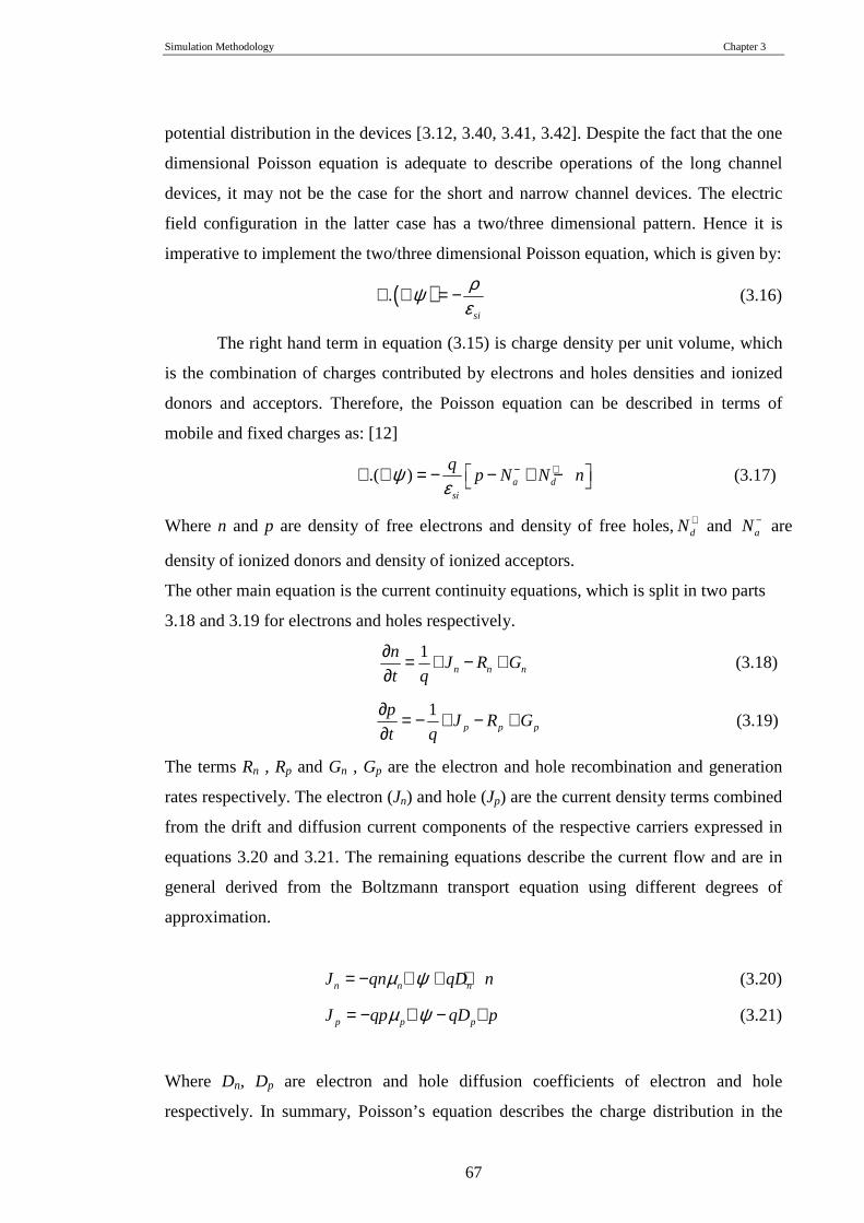
potential distribution in the devices [3.12, 3.40, 3.41, 3.42]. Despite the fact that the one
dimensional Poisson equation is adequate to describe operations of the long channel
devices, it may not be the case for the short and narrow channel devices. The electric
field configuration in the latter case has a two/three dimensional pattern. Hence it is
imperative to implement the two/three dimensional Poisson equation, which is given by:
( ).si
ρψε
∇ ∇ = − (3.16)
The right hand term in equation (3.15) is charge density per unit volume, which
is the combination of charges contributed by electrons and holes densities and ionized
donors and acceptors. Therefore, the Poisson equation can be described in terms of
mobile and fixed charges as: [12]
.( ) a dsi
qp N N nψ
ε− + ∇ ∇ = − − + − (3.17)
Where n and p are density of free electrons and density of free holes, dN+ and aN− are
density of ionized donors and density of ionized acceptors.
The other main equation is the current continuity equations, which is split in two parts
3.18 and 3.19 for electrons and holes respectively.
1
n n n
nJ R G
t q
∂ = ∇ − +∂
(3.18)
1
p p p
pJ R G
t q
∂ = − ∇ − +∂
(3.19)
The terms Rn , Rp and Gn , Gp are the electron and hole recombination and generation
rates respectively. The electron (Jn) and hole (Jp) are the current density terms combined
from the drift and diffusion current components of the respective carriers expressed in
equations 3.20 and 3.21. The remaining equations describe the current flow and are in
general derived from the Boltzmann transport equation using different degrees of
approximation.
n n nJ qn qD nµ ψ= − ∇ + ∇ (3.20)
p p pJ qp qD pµ ψ= − ∇ − ∇ (3.21)
Where Dn, Dp are electron and hole diffusion coefficients of electron and hole
respectively. In summary, Poisson’s equation describes the charge distribution in the
Simulation Methodology Chapter 3
68
semiconductor devices and the continuity equation treats the transport property of
carriers and the current generated by the dynamics of these carriers.
3.3.2 Comparisons of the diverse approaches to tran sport simulation
More complex but time consuming quantum techniques like non-equilibrium
Green’s function (NEGF) [3.43][3.44] and Wigner-function [3.45][3.46] are beyond the
scope of this work. Therefore, this work focuses mainly on the classical simulations
with quantum corrections which may be implemented to capture some of the quantum
mechanical effect on sub 100 nm MOSFETs. Generally there are three main categories
of device simulation methods applied to TCAD, namely the drift diffusion (DD), the
hydrodynamic (HD), and the Monte Carlo (MC) device simulation approaches.
Figure 3:6 illustrates the hierarchy and the relative accuracy of the
approximation of the carrier transport by the different device simulation models [3.47].
Since detailed analysis of these models is not the intention of this work, only a
comparative over view of the leading concepts of the three (highlighted in figure 3:6)
main approaches will be discussed.
One of the three main streams of device simulation approaches is the MC. It is a
particle approach that combines periods of deterministic free-flight with stochastic
scattering process implemented to approximate carrier dynamics in MOSFETs. MC uses
random number generator to calculate the stochastic motion of particles and their scattering
mechanisms [3.47]. The bigger the statistical sampling of the particle motion the better MC
simulation approximates the distribution function.
There are different types of MC simulation methods (single particle, ensemble, and
self consistent MC). For device simulations the self consistent MC approach is suitable,
since it solves the Poisson equation self consistently to determine electrostatic potential
distribution in the device. MC simulation does not make any assumption about the
distribution function to approximate the carrier transport [3.47] [3.48] and the carriers are
considered as a particles rather than as a fluid, which makes the MC approach more general
and accurate in approximating the carrier transport than the other two approaches.
The second approach to device simulation is the HD. In addition to the charge
conservation approach inherent in the DD model (explained next), the HD model
incorporates conservation of momentum (p) and energy (W) [3.49]. This will give the HD
approach a better approximation of the carrier energy and temperature gradient than the DD
approach. However the HD model has its own limitation. The problem with HD approach is
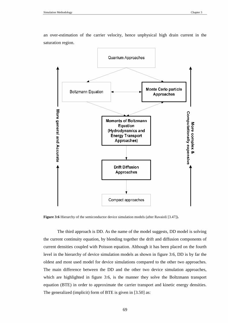
Simulation Methodology Chapter 3
69
an over-estimation of the carrier velocity, hence unphysical high drain current in the
saturation region.
Figure 3:6 Hierarchy of the semiconductor device simulation models (after Ravaioli [3.47]).
The third approach is DD. As the name of the model suggests, DD model is solving
the current continuity equation, by blending together the drift and diffusion components of
current densities coupled with Poisson equation. Although it has been placed on the fourth
level in the hierarchy of device simulation models as shown in figure 3:6, DD is by far the
oldest and most used model for device simulations compared to the other two approaches.
The main difference between the DD and the other two device simulation approaches,
which are highlighted in figure 3:6, is the manner they solve the Boltzmann transport
equation (BTE) in order to approximate the carrier transport and kinetic energy densities.
The generalized (implicit) form of BTE is given in [3.50] as:
Simulation Methodology Chapter 3
70
. ( , , )F.r pc
F fu f F s x p t
t t
∂ ∂+ ∇ + ∇ = +∂ ∂
(3.22)
where r is the particle position, p is the momentum, F is the electric field and the right
hand side of the equation describes all the scattering and collision events. The solution
of BTE is the distribution function (f) with seven dimensional spaces. [3.51]
The DD approach is based on the assumptions that electrons are in thermal
equilibrium with lattice temperature, therefore the continuity equation is based on the
conservation of charges given by
( ).n t nv∂ ∂ = ∇ (3.23)
but at high electric field-region carriers gain more kinetic energy influenced by the
strong field. This affects the average carrier temperature which is directly proportional
to the thermal kinetic energy (32 BTk ). As a result of an increase in the average total
energy ( 23 12 2Bk T mv+ ), there will be a high carrier temperature and velocity overshoot.
As reported in [3.52] it is possible that the carrier temperature could reach up to
twice the lattice temperature. Generally speaking the DD model does not estimate the
carrier velocity properly [3.53], which results in drain current underestimation. The
other assumption made by the DD model is to neglect the external forces during the
calculation of carrier energy. This means the carrier energy is approximated solely on
the basis of the local electric field [3.51] [3.54] but it depends on the global transport
state of the inversion layer [3.47].
3.3.3 Implemented physical models
The device structure that will be used as a prototype model for device simulation
is process simulated based on the continuous doping process. The introduction of
discrete doping and atomistic aspect of device simulation will be discussed elsewhere in
the thesis. Information of the device structure and doping profiles were fed into the
device simulation models as an input. The drift diffusion approach has been used
predominantly in the project as a compromise between accuracy and the computational
demand of the 3D statistical simulations of intrinsic parameter fluctuations effects. The
perpendicular electric field, the parallel electric field, and the concentration dependant
mobility models were used. We have also used a modified local density approximation
Simulation Methodology Chapter 3
71
(MLDA) model to approximate the quantum mechanical effect in the simulated deep
sub-micron devices. The brief review on each of these models has been presented.
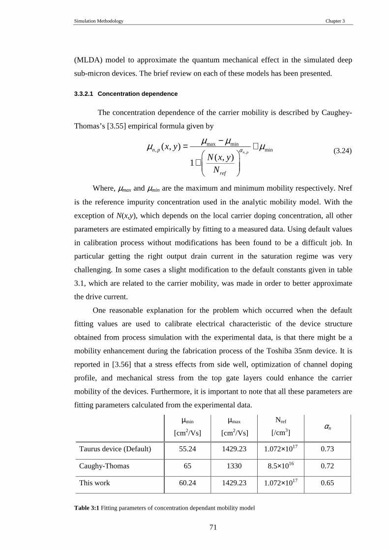
3.3.2.1 Concentration dependence
The concentration dependence of the carrier mobility is described by Caughey-
Thomas’s [3.55] empirical formula given by
,
max min, min( , )
( , )1
n pn p
ref
x yN x y
N
αµ µµ µ−= +
+
(3.24)
Where, µmax and µmin are the maximum and minimum mobility respectively. Nref
is the reference impurity concentration used in the analytic mobility model. With the
exception of N(x,y), which depends on the local carrier doping concentration, all other
parameters are estimated empirically by fitting to a measured data. Using default values
in calibration process without modifications has been found to be a difficult job. In
particular getting the right output drain current in the saturation regime was very
challenging. In some cases a slight modification to the default constants given in table
3.1, which are related to the carrier mobility, was made in order to better approximate
the drive current.
One reasonable explanation for the problem which occurred when the default
fitting values are used to calibrate electrical characteristic of the device structure
obtained from process simulation with the experimental data, is that there might be a
mobility enhancement during the fabrication process of the Toshiba 35nm device. It is
reported in [3.56] that a stress effects from side well, optimization of channel doping
profile, and mechanical stress from the top gate layers could enhance the carrier
mobility of the devices. Furthermore, it is important to note that all these parameters are
fitting parameters calculated from the experimental data.
Table 3:1 Fitting parameters of concentration dependant mobility model
µmin
[cm2/Vs]
µmax
[cm2/Vs]
Nref
[/cm3] αn
Taurus device (Default) 55.24 1429.23 1.072×10¹⁷ 0.73
Caughy-Thomas 65 1330 8.5×10¹⁶ 0.72
This work 60.24 1429.23 1.072×10¹⁷ 0.65
Simulation Methodology Chapter 3
72
For the sake of clarity, default values for Taurus device simulator, and the original
values estimated numerically in [3.55] are given in table 3.1. With the exception of αn,
all the default fitting parameters recommended in the Taurus device simulator have been
maintained as they are specified in table 3.1. During the device simulation of the 35nm
Toshiba device, we have changed αn, for n-type MOSFET, from its default value of 0.73
to 0.65 in order to calibrate the saturation drain current with the experimental data.
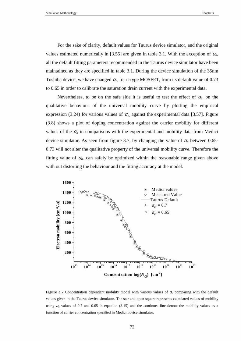
Nevertheless, to be on the safe side it is useful to test the effect of αn, on the
qualitative behaviour of the universal mobility curve by plotting the empirical
expression (3.24) for various values of αn, against the experimental data [3.57]. Figure
(3.8) shows a plot of doping concentration against the carrier mobility for different
values of the αn in comparisons with the experimental and mobility data from Medici
device simulator. As seen from figure 3.7, by changing the value of αn between 0.65-
0.73 will not alter the qualitative property of the universal mobility curve. Therefore the
fitting value of αn. can safely be optimized within the reasonable range given above
with out distorting the behaviour and the fitting accuracy at the model.
1013 1014 1015 1016 1017 1018 1019 1020 1021 1022
200
400
600
800
1000
1200
1400
1600
Ele
ctro
n m
obili
ty [
cm/V
-s]
Concentration log(Na) [cm-3]
Medici values Measured ValueTaurus Default αn = 0.7
αn = 0.65
Figure 3:7 Concentration dependant mobility model with various values of αn comparing with the default
values given in the Taurus device simulator. The star and open square represents calculated values of mobility
using αn values of 0.7 and 0.65 in equation (3.15) and the continues line denote the mobility values as a
function of carrier concentration specified in Medici device simulator.
Simulation Methodology Chapter 3
73
3.3.2.2 Perpendicular Electric-Field Dependence
The perpendicular electric-field dependence of the carrier mobility accounts for
the mobility reduction due to interface roughness scattering. The model used is based on
the works of Yamaguchi [3.58]. The original model was proposed to treat the mobility
as function of both parallel and perpendicular fields which is given by
( , , ) ( , ) ( )d o dN E E f N E g Eµ µ⊥ ⊥=� � (3.25)
In the Taurus device simulator, equation (3.25) has been modified as shown in (3.26) so
that it will take in to account only the perpendicular component of the field.
( ) ( )oE g Eµ µ⊥ ⊥= (3.26)
Where 0.5(1 )g Eα −⊥= + accounts for the property of the surface mobility and α is a
fitting parameter determined from the experimental data and is estimated as
51.539 10 /cm V−× for n-channel device and 55.35 10 /cm V−× for p-channel devices. ||E
and ⊥E are the parallel and perpendicular electric fields respectively.
3.3.2.3 Parallel Electric-Field Dependant Mobility Model:
The parallel electric field dependence of the mobility model is modified using
the expression reported in [3.55] given by:
0
1c
E
E
β
β
µµ =
+
(3.27)
Where E and Ec are the electric field and critical electric field and 0 /sat cv Eµ = is low
field mobility for constant concentration. In Taurus Device simulation software
equation (3.27) is modified to accommodate saturation velocity and the parallel electric
field component in a modified form given as
//1
s
s
satv
β
β
µµµ
= Ε+
(3.27b)
Simulation Methodology Chapter 3
74
Since the doping concentration is not constant µ0 is replaced by µs, which may take into
account the carrier scattering effects. The constant 1β = for holes and 2β = for
electrons are determined by fitting to experimental data [3.55].
3.3.2.4 Quantum Mechanical Effect - Modified Local Density Gradient Approximation
Quantum mechanical (QM) effect has a big influence on the operation of nano
scale CMOS device parameters and their electrical characteristics. The miniaturization
of electronic devices to a physical gate length of 7nm at the end of current ITRS
roadmap demands extraordinarily thin gate oxide (0.5 – 0.6nm) and very high channel
doping (well above the solid-solubility limit of known dopants in silicon). This creates a
strong electric field ( a
si
qNE
x ε∂ ≈∂
;ox
1
tE ∝ ) responsible for the quantization of carrier
motion in the direction normal to the interface [3.59]. This quantization of carriers
influences the device behaviour by, for example, increasing the subthreshold voltage
and decreasing the drive current of MOSFETs. To account for the QM effect during the
calibration and simulation of scaled devices, the modified local density gradient
approximation (MLDA) [3.60] has been included.
3.3.2.5 Glasgow Atomistic Device Simulator: 3-D
In order to investigate the intrinsic parameter fluctuations due to the discreteness
and randomness of dopants position and their number, the Glasgow atomistic device
simulator has been employed [3.9][3.33][3.61]. The 3-D Glasgow atomistic simulator is
based on the drift diffusion approach to solve the semiconductor equations (Poisson and
current continuity) with a quantum correction (density gradient).
To perform 3-D atomistic device simulation, the discrete random doping
distribution of devices must be generated. It can be generated from the continuous
doping profile by placing the dopant atom on the node and then deciding (by a rejection
technique) whether the placed atom is a silicon or a dopant by using the probability that
a dopant exists at a particular node ( ap N V= ). Alternatively, the discrete doping profile
can be extracted from the output device structure obtained by DADOS process
simulator (for further explanation see section 3.25).
Furthermore, the 3D Glasgow atomistic device simulator is fairly generic. It can
be adapted to perform atomistic device simulation on device structures different than the
conventional MOSFET ones. For example, the silicon on insulator (SOI) [3.62] and
Simulation Methodology Chapter 3
75
double gate devices have been investigated for intrinsic parameter fluctuations [3.63].
Recently, the density gradient transport model has been incorporated to the 3-D
atomistic device simulator so that it is possible to investigate the quantum mechanical
effect in the presence of discrete random dopants in decanano devices [3.64]. Practically
the major causes intrinsic parameter fluctuation, for example LER, random dopants, and
oxide thickness fluctuations can be simulated using the 3-D Glasgow atomistic device
simulator.
3.4 Chapter summary
In this chapter, the main simulation methodologies and TCAD tools have been
described. This includes the explanation of the fundamental concept of an integrated
process and device simulation in 3D. It has been illustrated in detail how different
TCAD simulation tools are systematically used during the process of this research work.
By doing so, we have introduced a consistent process and device simulation approach
for investigating the intrinsic parameter fluctuation due to the random dopants position
and number in scaled devices according to the technology roadmap.
Comparative descriptions of the mainstream approaches of solving the
semiconductor equations are presented. While the particle based Monte Carlo device
simulation approach captures more accurately the high-field carrier transport the
hydrodynamic model over-estimates the drive current. Although drift-diffusion is most
suitable for the long channel devices, with the introduction of quantum correction it can
captures reasonably well both the electrostatic behaviour and the properties of carrier in
the saturated region.
When the dimensions of semiconductor devices decrease the electric field
distribution increasingly shows two/three dimensional characteristics. This is due to the
inhomogeneous property of the parallel electric field in the depletion region. Therefore
the consideration of both the parallel electric field and the perpendicular electric field
mobility model is important. In addition, to account for the spatial variations of carrier
concentration, the concentration dependent mobility model has been used. Finally
quantum mechanical effects have also to be taken into account by including the local
density gradient approximation model. In the next chapter, the implementations of all
the methodologies, which have been discussed here, are presented.
Simulation Methodology Chapter 3
76
3.5 Chapter 3 references [3.1] S. Inaba et al., “High Performance 35nm Gate Length CMOS with NO Oxynitride
Gate Dielectric and Ni Salicide”, IEDM Technical Digest, pp. 641, 2001
[3.2] Semiconductor Industry Association, International Technology Roadmap for
Semiconductor Industry: ITRS’03 edition, Austin, Texas: 2003
[3.3] G. E. Moore, “Cramming more components onto integrated circuit”, Electronics,
April 19, 1965
[3.4] F.M. Schellenberg, “Lithography: The integration of TCAD and EDA”
Semiconductor International, Vol.27 (2), February 2004
[3.5] M. E. Law, “Process modelling for future technologies”, IBM J. RES. & DEV, Vol.
46, NO. 2/3, March/May 2002
[3.6] A. Asenov, M. Jaraiz, S. Roy, G. Roy, F. Adamu-Lema, A. R. Brown, V. Moroz,
and R. Gafiteanu, “Integrated Atomistic Process and Device Simulation of
Decananometer MOSFETs”, SISPAD 2001, pp.
[3.7] M. Jaraiz, P. Castrillo, R. Pinacho, I. Martin-Bragado, and J. Barbolla, “Atomistic
Front-End Process Modelling: A Powerful Tool for Deep-Submicron Device
Fabrication,” Proc. SISPAD 2001, pp. 10-17, 2001.
[3.8] N. Strecker, V. Moroz, and M. Jaraiz, “Introducing Monte Carlo Diffusion
Simulation into TCAD Tools,” Proc. ICCN 2002, pp. 247-250, 2002.)
[3.9] A. Asenov, “Random dopant Induced Threshold Voltage Lowering and Fluctuations
in Sub-0.1 µm MOSFET’s: A 3-D “Atomistic” Simulation study”, IEEE Tras.
Electron Devices. Vol. 45(12), pp. 2505-2513, 1998
[3.10] N. E. B. Cowen, M. Jaraiz, F. Cristiano, A. Claverie, and G. Mannino,
“Fundamental Diffusion Issues for Deep-Submicron Device Processing”, IEDM
Tech. Dig. pp. 333-336, 1999
[3.11] Synopsys Taurus-TSUPREM4, Taurus-Process Reference manual, Version V2003-
12, December 2003
[3.12] Y. Taur, T. H. Ning, “Fundamentals of modern VLSI devices ”, Cambridge
University Press, Cambridge, UK, 1998
[3.13] M.D.Giles, “Ion implantation”, in VLSI Technology, edited by S. M. Sze, 2nd
Edition, McGraw-Hill International Edition, pp. 327-375, 1988
[3.14] W. Shockley, “Forming Semi-conductive Devices by Ionic Bombardment”, US
Patent number 2787564

Simulation Methodology Chapter 3
77
[3.15] B. R. Fair, “History of Some Early Developments in on-Implantation
Technology Leading to Silicon Transistor Manufacturing”, Proceedings of the
IEEE, VOL. 86, NO. 1, pp. 111-137, January 1998
[3.16] S. Tian, M. F. Morris, S. J. Morris, B. Obradovic, G. Wang, Al F. Tasch, and C. M.
Snell, “A detail Physical Model For Ion Implant Induced Damage in Silicon”, IEEE
Tran. Elec. Dev. Vol. 45, pp. 1226 June 1998
[3.17] K. W. Böer, “Survey of Semiconductor Physics” Volume 2, Barriers, Junctions,
Surfaces, and Devices, Van Nostrand Reinhold, New York, 1992
[3.18] P.Bouillon, et al., “Re-Examination of Indium implantation for a low power 0.1µm
technology”, IEDM95 Tech. Dig. , pp. 897-900, 1995
[3. 19] P.B. Griffin, M. Cao, P. Vande Voorde, Y. –L. Chang, and W. M. Greene, “Indium
transient enhanced diffusion”, Applied Physics Letters, Vlo. 73, pp. 2986,
November 1998
[3.20] H. Liao, D. S. Ang and C. H. Ling, “A Comprehensive Study of Indium
Implantation-Induced Damage in Deep Sub-micrometer n-MOSFET: Device
Characterization and Damage Assessment”, IEEE Trans. Elec. Dev. Vol. 49,
pp.2254, December 2002.
[3.21] J. W. Mayer, L. Eriksson, and J. A. Davies, “Ion Implantation in Semiconductors:
Silicon and Germanium ”, Academic Press, New York, 1970
[3.22] J. Lindhard, M. Scharff, and H.E. Schioit, “Range Concepts and Heavy ion
Rangers”, Notes on Atomic Collisions, II Mat.-Fys Med. Dan Vid Selsk., Bind 33,
No. 14, 1963
[3.23] J. F. Gibbons, W. S. Johnson, S. W. Mylroie, “Projected Range Statistics,
Semiconductors and Related Materials”, Dowden, Hutchinson & Ross, 2nd Edition,
1975
[3.24] A. Stuart, J. K. Ord, Kendall’s Advanced Theory of Statistics, Volume 1,
Distribution Theory, 2nd Edition, Edward Arnold, London 1994
[3.25] Al. F. Tasch, H. Shin, C. Park, J. Alvis, S. Novak, “An Improved Approach to
Accuratly Model Shallow B and BF2 Implants in Silicon”, J. Electrochemical Soc.
Vol. 136, No. 3, pp. 810-814, 1989
[3.26] S. Selberherr, “Process and Device Modelling for VLSI”, Macroelectron Reliab.,
Vol. 24, No. 2, pp. 225-257, 1984
Simulation Methodology Chapter 3
78
[3.27] W. P. Peterson, W. Fichtner, and E. H. targets, “Vectorized Monte Carlo
Calculation for the Transport of Ions in Amorphous Targets”, IEEE Trans. Electron
Devices, Vol. 30, No. 9, pp. 1011-1017, 1983
[3.28] P. M. Fahey, P. B. Griffin, and J. D. Plummer, “Point defects and dopant diffusion
in silicon”, Review of Modern Physics, Vol. 61, No. 2, pp. 289, April 1989
[3.29] J. C. C. Tsai, “Diffusion”, in VLSI Technology, 2nd Edition, Edited by S. M. Sze,
McGraw-Hill International Edition, pp. 272-326, 1988
[3.30] A. M. Smith, in Fundamentals of Silicon Integrated Device Technology, Volume I,
Edited by Burger and Donovan, Series in Solid State Physical Electronics, Prentice
Hall, pp. 181-345, 1967
[3.31] S.M. Sze, Semiconductor Devices: Physics and Technology, 2nd Edition, John Wiley
and Sons, USA, 2002
[3.32] D. J. Frank, Y. Taur, M. Ieong, and H.-S. P. Wong, “Monte Carlo Modelling of
Threshold Variation due to Dopant Fluctuation”, Symposium on VLSI circuit Digest
of technical Papers, pp. 171-172, 1999
[3.33] A. Asenov, Gabriela Slavcheva, Andrew R.Brown, John H. Davis, and Subhash
Saini, “Increase in the Random Dopant Induced Threshold Fluctuations and
Lowering in Sub-100nm MOSFETs Due to Quantum Effects: A 3-D Density
Gradient Simulation Study”, IEEE Trans. Electron Devices, Vol. 48(4), pp. 722-
729, 2001
[3.34] M. Jaraiz, G.H. Gilmer, J. M. Poate, and T.D. de la Rubia, “Atomistic calculation of
ion implantation in Si: Point defect and transient enhanced diffusion phenomena”,
Apply. Phys. Lett. Vol. 68(3), pp. 409-411, 1996
[3.35] M. Jaraiz, P. Castrillo, R. Pinacho, L. Pelaz, J. Barbolla, G. H. Gilmer and S. C.
Rafferty, “Atomistic Modeling of Complex Silicon Processing Scenarios ” Mat.
Res. Soc. Symp. Proc. Vol. 610 p.B11.1-7, 2001
[3.36] B. E. Deal and A.S. Grove, “General relationship for Thermal Oxidation of
Silicon”, Journal of Applied Physics, Vol.36 (12), pp. 3770-3778, Dec. 1965
[3.37] R. P. Donovan, in Fundamentals of Silicon Integrated Device Technology, Volume
I, Edited by Burger and Donovan, Series in Solid State Physical Electronics,
Prentice Hall, pp. 3-180, 1967
[3.38] B. E. Deal, “Thermal Oxidation Kinetics of Silicon in Pyrogenic H2O and 5%
HCl/H2O Mixtures ”, Journal of Electrochemical Society, Vol. 125 (4), pp. 576,
1978
Simulation Methodology Chapter 3
79
[3.39] C. P. Ho. and J.D. Plummer, “Si/SiO2 Interface Oxidation Kinetics: A Physical
Model for the Influence of High Substrate Doping Levels”, Journal of
Electrochemical Society, Vol.126(9), pp. 1516-1530, 1979
[3.40] T. Ando, B. A. Fowler, F. Stren, “Electronic properties of two dimensional
systems”, Reviews of Modern Physics, Vol. 54, No. 2, pp. 437, April 1982
[3.41] S. M. Sze, Physics of Semiconductor Devices, Wiley International science, 1981
[3.42] S. Selberherr, “MOS Device Modelling at 77 K”, IEEE Trans. Electron Dev.
Vol.36, pp. 1464-1474, 1989
[3.43] Z. Ren, R. Venugopal, S., Datta, and M. Lundstrom, “Examination of design and
manufacturing issues in a 10 nm double gate MOSFET using non-equilibrium
Green's function simulation”, IEDM Tech. Dig., pp, 107-110, December 2001
[3.44] S. Datta, “The non-equilibrium Green function (NEGF) formalism: An elementary
introduction”, IEDM Tech. Dig., pp, 703-706, December 2002
[3.45] L. Shifren, and D. K. Ferry, “Wigner Function Based Monte Carlo Approach for
Accurate Incorporation of Quantum Effects in Device Simulation”, Journal of
Computational Electronics, 1: 55-58, 2002
[3.46] P. Bordone, and C. Jacoboni “Wigner Paths for Quantum Transport”, Journal of
Computational Electronics, 1: 67-73, 2002
[3.47] U. Ravaioli “Hierarchy of simulation approaches for hot carrier transport in deep
submicron devices”, Semicond. Sci. Technol., Vol. 13, pp. 1-10, 1998
[3.48] K. Tomizawa, Numerical Simulation of Submicron Semiconductor Devices, Artech
House, Boston, London, 1993
[3.49] P. Lugli, “The Monte Carlo Method for Semiconductor device and Process
Modelling”, IEEE Trans. On Computer-aided Design, Vol. 9(11), 1999
[3.50] M. Lundstrom, Fundamentals of carrier transport, Second edition, Cambridge, UK:
Cambridge University Press, pp. 119-157 , 2000
[3.51] S. Selberherr, Analysis and Simulation of Semiconductor devices, New York:
Springer-Verlag, 1984
[3.52] T. Grasser, T - W. Tang, H. Kosina, S. Selberherr, “A Review of Hydrodinamic and
Energy-Transport Models for Semiconductor Device Simulation”, Proceedings of
the IEEE, Vol. 91(2), pp. 251-274, 2003
[3.53] J.D. Bude “MOSFET Modelling Into Ballistic Regime”, in Proc. Simulation
Semiconductor Processes and Devices, SISPAD 2000, pp. 23-26, 2000
Simulation Methodology Chapter 3
80
[3.54] T. Grasser, H. Kosina, and S. Selberher, “Consistent Comparison of Drift-Diffusion
and Hydro-Dynamic Device Simulations”, in Proc. Simulation Semiconductor
Processes and Devices, SISPAD’ 99, pp.151-154, 1999
[3.55] D.M. Caughey, and R. E. Thomas, “Carrier Motilities in Silicon Empirically
Related to Doping and Field”, Proceedings of the IEEE, Vol. 55, pp. 2192, 1967
[3.56] T. Sugii, K. Watanabe, and S. Sugatani, “Transistor Design for 90nm-Generation
and Beyond”, Fujitsu Sci. Tech. J., Special Issue: Advanced Silicon Device
Technologies, Vol. 39 (1), pp.9-22, 2003
[3.57] W.R.Thurber, R. L. Mattis, and Y.M. Liu, and J. J. Filliben, “Resistivity-Dopant
Density Relationship for Phosphorus-Doped Silicon”, J. Electrochem. Soc. Vol. (8),
1807-1812, 1980
[3.58] K. Yamaguchi, “Field-Dependant Mobility Model for analysis of MOSFET’s”,
IEEE Trans. Electron Dev., Vol. 26, No. 7, pp. 1068-1074, 1979
[3.59] F. Stern, and W. E. Howard, “Properties of Semiconductor Inversion Layers in The
Electric Quantum Limit”, Phys. Rev. Vol. 163 (3), 1967
[3.60] G. Paasch and H.Ubensee, “A Modified Local Density Approximation”, Phys. Stat.
Sol. (b), Vol. 113, pp. 165-178, 1982
[3.61] A. Asenov, Andrew R. John H. Davies, and Subhash Saini “Hierachical Approach
to “Atomistic” 3-D MOSFET Simulation”, IEEE Trans. Computer-Aided Design of
integrated Circuit and Systems, Vol. 18 (11), pp. 1558-1565, 1999
[3.62] A. R. Brown, FikruAdamu-Lema, and Asen Asenov, “Intrinsic parameter
fluctuations in nanometre scale thin-body SOI devices introduced by interface
roughness”, Super lattices and Microstructures, Vol. 34, pp. 283–291, 2003
[3.63] A. R. Brown, J. R. Watling, and A. Asenov, “Intrinsic Fluctuations in Sub 10-nm
Double-Gate MOSFETs Introduced by Discreteness of Charge and Matter”, IEEE
Trans on Nanotechnology , Vol. 1(4), pp. 195 – 200, 2002
[3.64] A. Asenov, G. Slavcheva, A. R. Brown, J. H. Davies, and S. Saini, “Increase in
the Random Dopant Induced Threshold Fluctuations and Lowering in Sub-100
nm MOSFETs Due to Quantum Effects: A 3-D Density-Gradient Simulation
Study”, IEEE Trans. Electron Devices, Vol. 48 (4), pp. 722-729, 2001
Related Documents