1718 IEEE JOURNAL OF SOLID-STATE CIRCUITS, VOL. 41, NO. 8, AUGUST 2006 3-D Silicon Integration and Silicon Packaging Technology Using Silicon Through-Vias John U. Knickerbocker, Member, IEEE, Chirag S. Patel, Paul S. Andry, Cornelia K. Tsang, L. Paivikki Buchwalter, Edmund J. Sprogis, Hua Gan, Raymond R. Horton, Robert J. Polastre, Steven L. Wright, and John M. Cotte Abstract—System-on-Chip (SOC) and System-on-Package (SOP) technologies each have advantages depending on ap- plication needs. As system architects and designers leverage ever-increasing CMOS technology densities, a range of two- and three-dimensional silicon integration technologies are emerging which will likely support next-generation high-volume electronic applications and may serve high-performance computing applica- tions. This paper will discuss a few emerging technologies which offer opportunities for enhanced circuit performance, or reduced power as one example. Silicon-on-silicon integration may include three-dimensional (3-D) integration on-chip or may leverage chip stacking or chip integration on package. Common technology features include silicon through-vias, high-I/O interconnection and silicon-on-silicon either as 3-D integrated circuits, integrated chip stacks or silicon-on-silicon packages with passive function or high-bandwidth wiring. Silicon chips on silicon interposers with integrated function such as decoupling capacitors may provide a better module architecture compared to increased on-chip decoupling or off chip discrete capacitors mounted on package at the chip perimeter or underside of the package. Advanced silicon carrier package technology with fine pitch (50 m) interconnec- tion is described. This silicon carrier package contains silicon through-vias and offers 16 increase over standard chip I/O, a 20 to 100 increase in wiring density over traditional organic and ceramic packaging, and allows for integrated high-perfor- mance passives. Silicon carrier technology supports lithographic scaling and provides a basis for known good die (KGD) wafer testing. It may be considered for use in a number of applications including optoelectronic (OE) transceivers, silicon interposers with integrated decoupling capacitors, and mini-multi-chip mod- ules (MMCMs) which integrate heterogeneous dies forming a single “virtual chip.” Index Terms—Chip integration, high bandwidth, integrated decoupling capacitors, interconnection, silicon packaging, silicon through-vias, 3-D. I. INTRODUCTION S YSTEM-ON-CHIP (SOC) has supported reduced costs and improved time-to-market [1] and has fueled semicon- ductor growth from pervasive electronic applications through Manuscript received December 5, 2005; revised March 17, 2006. This work was supported in part by the Defense Advanced Research Projects Agency (DARPA) under the Chip-to-Chip Optical Interconnects (C2OI) Program, Agreement MDA972-03-3-0004, in part by DARPA under the PERCS Pro- gram, Agreement NBCH30390004, and in part by the Maryland Procurement Office under Contract H98230-04-C-0920. J. U. Knickerbocker, C. S. Patel, P. S. Andry, C. K. Tsang, L. P. Buchwalter, R. R. Horton, R. J. Polastre, S. L. Wright, and J. M. Cotte are with the IBM T. J. Watson Research Center, Yorktown Heights, NY 10598 USA (e-mail: [email protected]). E. J. Sprogis is with the IBM T. J. Watson Research Center, Essex Junction, VT 05452 USA. H. Gan is with the IBM T. J. Watson Research Center, Hopewell Junction, NY 12533 USA. Digital Object Identifier 10.1109/JSSC.2006.877252 Fig. 1. Evolution of memory density over time [2]. more complex computing products. An example shown in Fig. 1 is the evolution of memory density over time [2] which shows support to Moore’s law [3] through 1998. Moore’s law states chip integration advancements are comprised of 50% lithography, 25% device and circuit innovations and 25% from chip size which collectively provide a performance doubling every 18 months. Fig. 1 also shows a slow down in memory density scaling post 1998. Is Moore’s law borken? Is circuit scaling coming to an end? Should we be considering alternate technologies? Chen has reported an expectation for continued CMOS circuit scaling but also shows a parallel roadmap ap- proach to provide subsystem scaling over time and development of post CMOS technologies and quantum computing [4]. For subsystem research, subsystem scaling may include 3-D silicon integration and 3-D packaging especially where increasing cores per processor chip need increasing bandwidth to memory for high-performance operation [4]. Package integration has also progressed over time with increasing perimeter and area array interconnection density, but the rate of integration has fallen far behind chip circuit integra- tion and has clearly not kept pace with Moore’s law even if the rate of chip integration has been reduced in recent years. For chip-to-package interconnection, area array (flip-chip) tech- nology has provided the highest level of chip integration using traditional organic and ceramic packages at I/O per cm . Higher density chip-to-package or three-dimensional (3-D) chip-to-chip integration may leverage silicon through-via in- terconnection, as is illustrated in Fig. 2. Chip stacking, silicon carrier packaging, and 3-D chip circuit and wiring integration offer an even higher level of silicon integration where orders of magnitude I/O density advancement may be possible. Tech- nology advancements and manufacturing learning are required 0018-9200/$20.00 © 2006 IEEE

Welcome message from author
This document is posted to help you gain knowledge. Please leave a comment to let me know what you think about it! Share it to your friends and learn new things together.
Transcript
1718 IEEE JOURNAL OF SOLID-STATE CIRCUITS, VOL. 41, NO. 8, AUGUST 2006
3-D Silicon Integration and Silicon PackagingTechnology Using Silicon Through-Vias
John U. Knickerbocker, Member, IEEE, Chirag S. Patel, Paul S. Andry, Cornelia K. Tsang, L. Paivikki Buchwalter,Edmund J. Sprogis, Hua Gan, Raymond R. Horton, Robert J. Polastre, Steven L. Wright, and John M. Cotte
Abstract—System-on-Chip (SOC) and System-on-Package(SOP) technologies each have advantages depending on ap-plication needs. As system architects and designers leverageever-increasing CMOS technology densities, a range of two- andthree-dimensional silicon integration technologies are emergingwhich will likely support next-generation high-volume electronicapplications and may serve high-performance computing applica-tions. This paper will discuss a few emerging technologies whichoffer opportunities for enhanced circuit performance, or reducedpower as one example. Silicon-on-silicon integration may includethree-dimensional (3-D) integration on-chip or may leverage chipstacking or chip integration on package. Common technologyfeatures include silicon through-vias, high-I/O interconnectionand silicon-on-silicon either as 3-D integrated circuits, integratedchip stacks or silicon-on-silicon packages with passive function orhigh-bandwidth wiring. Silicon chips on silicon interposers withintegrated function such as decoupling capacitors may providea better module architecture compared to increased on-chipdecoupling or off chip discrete capacitors mounted on package atthe chip perimeter or underside of the package. Advanced siliconcarrier package technology with fine pitch (50 m) interconnec-tion is described. This silicon carrier package contains siliconthrough-vias and offers 16 increase over standard chip I/O, a20 to 100 increase in wiring density over traditional organicand ceramic packaging, and allows for integrated high-perfor-mance passives. Silicon carrier technology supports lithographicscaling and provides a basis for known good die (KGD) wafertesting. It may be considered for use in a number of applicationsincluding optoelectronic (OE) transceivers, silicon interposerswith integrated decoupling capacitors, and mini-multi-chip mod-ules (MMCMs) which integrate heterogeneous dies forming asingle “virtual chip.”
Index Terms—Chip integration, high bandwidth, integrateddecoupling capacitors, interconnection, silicon packaging, siliconthrough-vias, 3-D.
I. INTRODUCTION
SYSTEM-ON-CHIP (SOC) has supported reduced costsand improved time-to-market [1] and has fueled semicon-
ductor growth from pervasive electronic applications through
Manuscript received December 5, 2005; revised March 17, 2006. This workwas supported in part by the Defense Advanced Research Projects Agency(DARPA) under the Chip-to-Chip Optical Interconnects (C2OI) Program,Agreement MDA972-03-3-0004, in part by DARPA under the PERCS Pro-gram, Agreement NBCH30390004, and in part by the Maryland ProcurementOffice under Contract H98230-04-C-0920.
J. U. Knickerbocker, C. S. Patel, P. S. Andry, C. K. Tsang, L. P. Buchwalter,R. R. Horton, R. J. Polastre, S. L. Wright, and J. M. Cotte are with the IBMT. J. Watson Research Center, Yorktown Heights, NY 10598 USA (e-mail:[email protected]).
E. J. Sprogis is with the IBM T. J. Watson Research Center, Essex Junction,VT 05452 USA.
H. Gan is with the IBM T. J. Watson Research Center, Hopewell Junction,NY 12533 USA.
Digital Object Identifier 10.1109/JSSC.2006.877252
Fig. 1. Evolution of memory density over time [2].
more complex computing products. An example shown inFig. 1 is the evolution of memory density over time [2] whichshows support to Moore’s law [3] through 1998. Moore’s lawstates chip integration advancements are comprised of 50%lithography, 25% device and circuit innovations and 25% fromchip size which collectively provide a performance doublingevery 18 months. Fig. 1 also shows a slow down in memorydensity scaling post 1998. Is Moore’s law borken? Is circuitscaling coming to an end? Should we be considering alternatetechnologies? Chen has reported an expectation for continuedCMOS circuit scaling but also shows a parallel roadmap ap-proach to provide subsystem scaling over time and developmentof post CMOS technologies and quantum computing [4]. Forsubsystem research, subsystem scaling may include 3-D siliconintegration and 3-D packaging especially where increasingcores per processor chip need increasing bandwidth to memoryfor high-performance operation [4].
Package integration has also progressed over time withincreasing perimeter and area array interconnection density, butthe rate of integration has fallen far behind chip circuit integra-tion and has clearly not kept pace with Moore’s law even if therate of chip integration has been reduced in recent years. Forchip-to-package interconnection, area array (flip-chip) tech-nology has provided the highest level of chip integration usingtraditional organic and ceramic packages at I/O per cm .Higher density chip-to-package or three-dimensional (3-D)chip-to-chip integration may leverage silicon through-via in-terconnection, as is illustrated in Fig. 2. Chip stacking, siliconcarrier packaging, and 3-D chip circuit and wiring integrationoffer an even higher level of silicon integration where ordersof magnitude I/O density advancement may be possible. Tech-nology advancements and manufacturing learning are required
0018-9200/$20.00 © 2006 IEEE
KNICKERBOCKER et al.: 3-D SILICON INTEGRATION AND SILICON PACKAGING TECHNOLOGY USING SILICON THROUGH-VIAS 1719
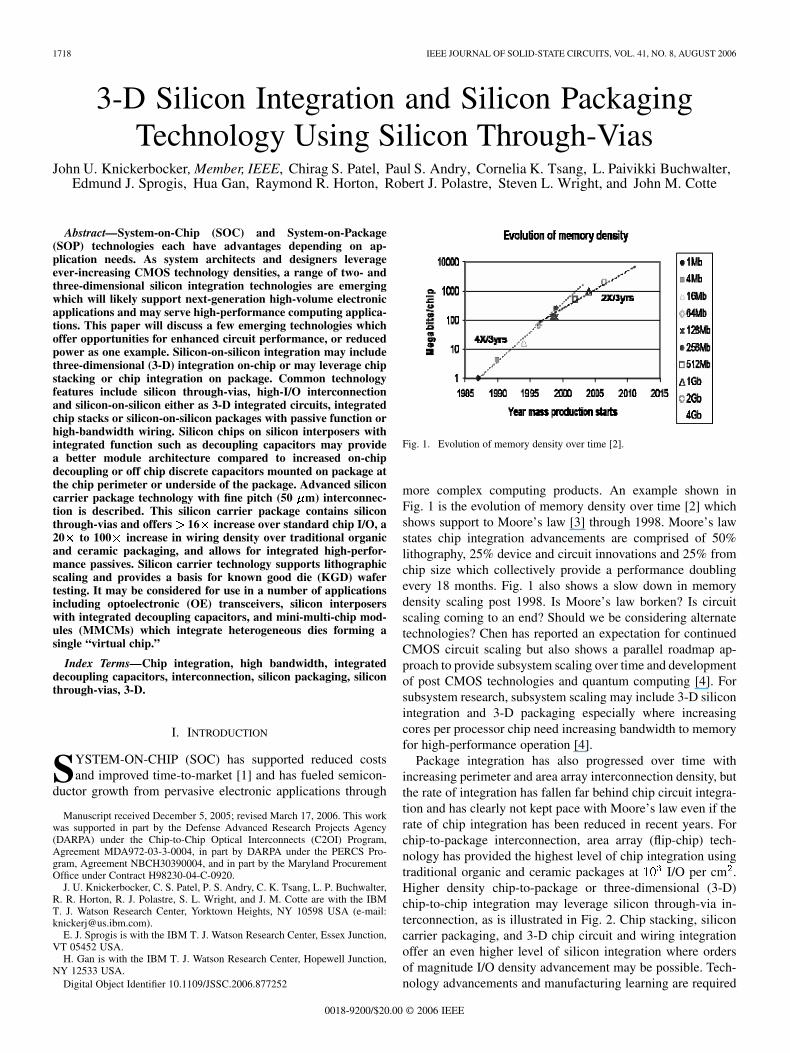
Fig. 2. Silicon integration comparison for ceramic and organic packaging, sil-icon carrier and chip stack and 3-D silicon circuits and wiring.
to overcome key challenges and to achieve lower costs. Ad-vantages include minaturization, increased bandwidth, higherperformance, reduced power, and the ability to integrate hetero-geneous technologies [5]–[7]. As depicted in Fig. 2, 3-D circuitintegration may hold the opportunity for the highest level ofcircuit integration with stacked active devices [5], [8] and mayrequire complete circuit and architecture design innovations ateach level or 3-D design tools to best take advantage of thisemerging technology. Chip stacking, silicon carrier, or siliconpackaging technologies shown with intermediate interconnec-tion density in Fig. 2 may provide another means to develop 3-Dstructures which enhance system integration and performance.Key technology challenges include design, design tools, test,alignment and assembly, and cooling, depending on the level ofintegration and power. Benefits in product quality and cost canbe expected as industry 3-D infrastructure and manufacturingmature.
Examples of silicon integration using SOP and SOC at IBMhave been reported for manufactured products and in researchdemonstrations. In high-performance server products usingSOP thin-film multi-chip modules [9] and ceramic modules[10], 97-3 PbSn solder interconnections up to 7018 signalI/O were used at 200- m pitch for a density up to 2500 I/Oper cm . Research on SOC advanced interconnection densityMEMS or VLSI-MEMS [6] has demonstrated interconnectiondensity at 300 electrical connections per mm (30 000 per cm )using 15- m-diameter copper studs with a tin cap and reporteda 99.9% yield. Research on a SOP silicon carrier used for aparallel optical tranceiver [7] demonstrated 25- m solder inter-connection at a 50- m pitch with a limited number of total I/Obut with a density of 40 000 I/O per cm using AuSn eutecticsolder to create a terabit per second parallel tranceiver module.A recent electrical integrity demonstration of a transferredring ocillator using 130-nm silicon-on-insulator (SOI) CMOSdevices and circuits [5] illustrates the potential opportunity toscale 3-D integrated circuits to a much higher level of SOCintegration. In each of these research demonstrations, a path
TABLE IEMERGING 3-D TECHNOLOGIES
forward to volume manufacturing should consider the businessapplications and manufacturing practices to enable productvalue at low cost. Practical considerations influencing 3-Dproduct definition using SOC versus SOP include the numberof devices to be integrated, testability and overall yield. Asummary of emerging 3-D technology integration is shownin Table I which includes 3-D circuits connected with areaarray silicon through-vias, 3-D cooling, 3-D MEMS, siliconpackaging and integration of these structures by SOC andSOP/SIP. An example of emerging technology is the newsilicon through-via compared to traditional back-end of linewiring and vias in the wafer build up layers.
Recent publications have described research including ap-proaches for 3-D integrated circuits and chip stacking, eachhaving vias which permit silicon-on-silicon stacking. In one ap-proach, SOI technology permitted very small vias to join activecircuits in two layers of silicon [5], [8]. In another approach,10- m copper conductors provided through silicon electrical in-terconnection at 20- m pitch [11]. Limited or no informationwas reported on the robustness of these via structures basedon application or reliability stressing. Fine-pitch interconnec-tion for silicon-on-silicon has also been reported with a widevariety of bonding and electrical interconnection approachesbetween silicon die in chip stacks or packages using silicon.For example, anistropic conductive polymers were used to bond25- m thinned die [12]. Fifty- m AuSn bumps [13] and fine-pitch solder have been reported to join silicon chips to stackedsilicon packages [14]. Cu studs with Sn cap have also been usedto join fine-pitch features between silicon chips in a stack [15].Limited data was reported on the manufacturability of thesetechnologies and their reliability toward product applications.
In this paper, we show examples of potential product appli-cations for 3-D silicon-on-silicon technology and silicon carrierpackaging technology. Examples of process flow for fabrica-tion and assembly are reported. A comparison of bandwidthbetween package options is shown. Examples of technologydemonstrations include: 1) silicon through-via structures; 2)
1720 IEEE JOURNAL OF SOLID-STATE CIRCUITS, VOL. 41, NO. 8, AUGUST 2006
electrical characterization of wiring on a silicon package; 3)assembly using PbSn and SnCu solder microbumps; 4) anexample of fine-pitch probes for wafer level testing; and 5)a summary of reliability testing results for the 50- m-pitchsolder interconnections.
II. SILICON CARRIER PACKAGING TECHNOLOGY
AND APPLICATIONS
Silicon carrier packaging technology includes: 1) siliconthrough-vias; 2) high-density signal wiring and voltage dis-tribution; 3) fine-pitch interconnection such as permanentcopper-to-copper stud bonding or reworkable high-I/O solderinterconnection; 4) high-I/O testing such as known good die(KGD) testing and assembled module testing; and 5) integratedfunction such as decoupling capacitors. The critical technologyneeds vary based on design, manufacturing, application andrelative cost compared to competing solutions. Discussedbelow are three potential applications of IBM’s silicon carriertechnology.
First, a parallel optical transceiver integrating heterogeneouscomponents on a silicon carrier package as has been previouslyreported by Patel et al. [7] is discussed. Second, a silicon car-rier package having integrated decoupling capacitance as aninterposer directly under an active chip is presented. Third, ahigh-density package with high-density interconnection for in-terconnecting multiple chips or chip stacks as a mini-multi-chipmodule (MMCM) or “virtual chip” is detailed.
III. PARALLEL OPTICAL TRANSCEIVER
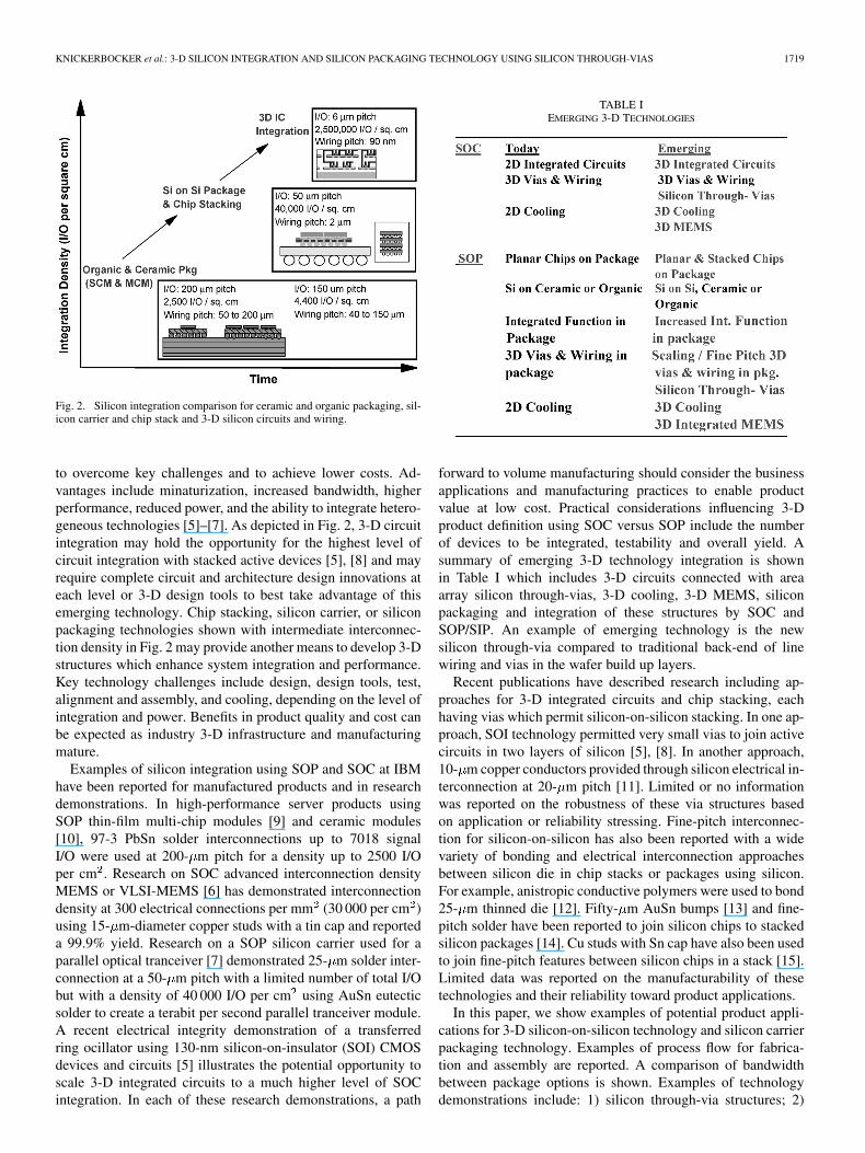
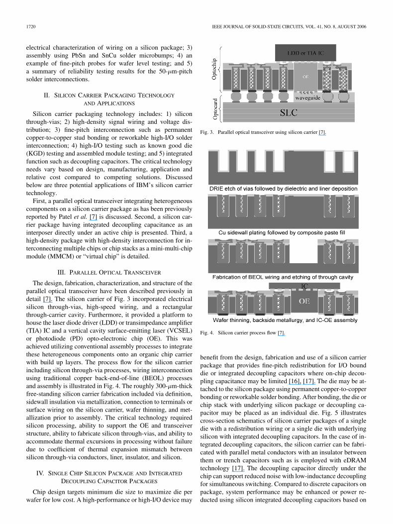
The design, fabrication, characterization, and structure of theparallel optical transceiver have been described previously indetail [7]. The silicon carrier of Fig. 3 incorporated electricalsilicon through-vias, high-speed wiring, and a rectangularthrough-carrier cavity. Furthermore, it provided a platform tohouse the laser diode driver (LDD) or transimpedance amplifier(TIA) IC and a vertical cavity surface-emitting laser (VCSEL)or photodiode (PD) opto-electronic chip (OE). This wasachieved utilizing conventional assembly processes to integratethese heterogeneous components onto an organic chip carrierwith build up layers. The process flow for the silicon carrierincluding silicon through-via processes, wiring interconnectionusing traditional copper back-end-of-line (BEOL) processesand assembly is illustrated in Fig. 4. The roughly 300- m-thickfree-standing silicon carrier fabrication included via definition,sidewall insulation via metallization, connection to terminals orsurface wiring on the silicon carrier, wafer thinning, and met-allization prior to assembly. The critical technology requiredsilicon processing, ability to support the OE and transceiverstructure, ability to fabricate silicon through-vias, and ability toaccommodate thermal excursions in processing without failuredue to coefficient of thermal expansion mismatch betweensilicon through-via conductors, liner, insulator, and silicon.
IV. SINGLE CHIP SILICON PACKAGE AND INTEGRATED
DECOUPLING CAPACITOR PACKAGES
Chip design targets minimum die size to maximize die perwafer for low cost. A high-performance or high-I/O device may
Fig. 3. Parallel optical transceiver using silicon carrier [7].
Fig. 4. Silicon carrier process flow [7].
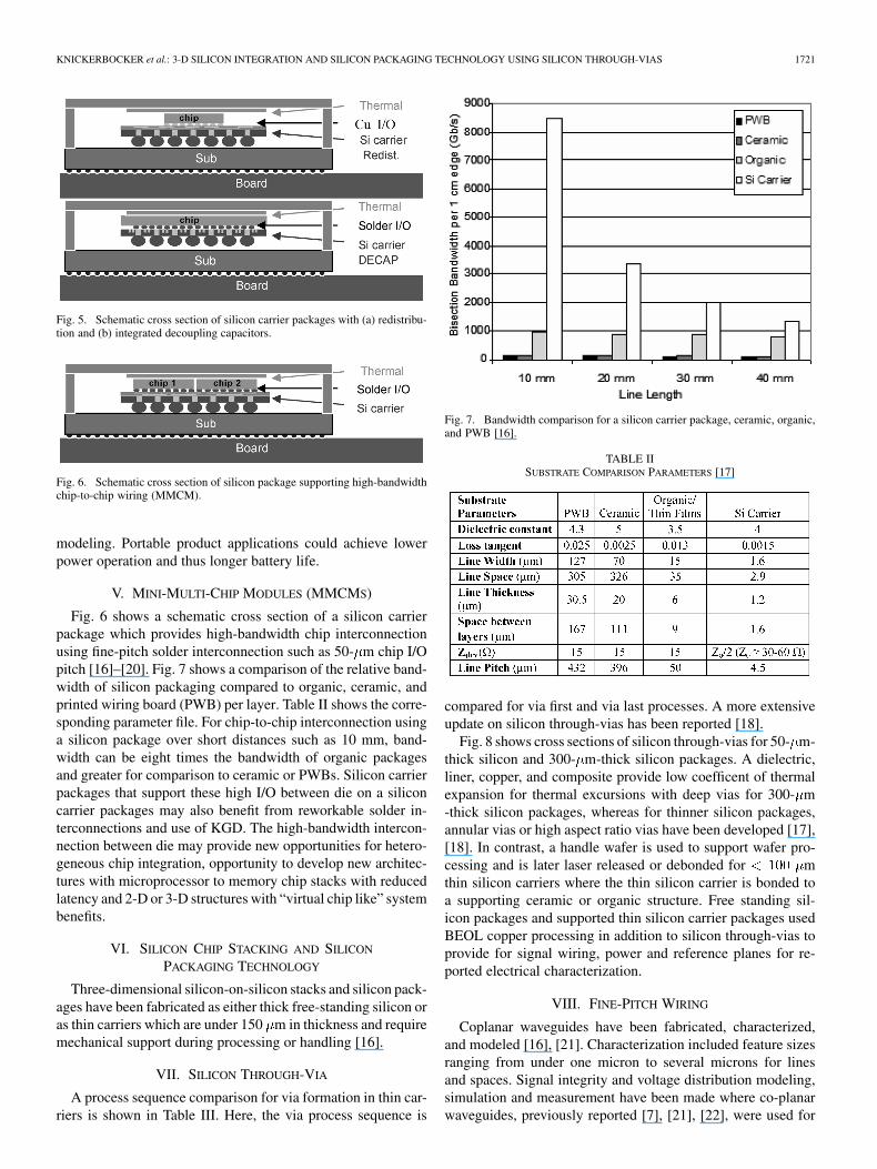
benefit from the design, fabrication and use of a silicon carrierpackage that provides fine-pitch redistribution for I/O bounddie or integrated decoupling capacitors where on-chip decou-pling capacitance may be limited [16], [17]. The die may be at-tached to the silicon package using permanent copper-to-copperbonding or reworkable solder bonding. After bonding, the die orchip stack with underlying silicon package or decoupling ca-pacitor may be placed as an individual die. Fig. 5 illustratescross-section schematics of silicon carrier packages of a singledie with a redistribution wiring or a single die with underlyingsilicon with integrated decoupling capacitors. In the case of in-tegrated decoupling capacitors, the silicon carrier can be fabri-cated with parallel metal conductors with an insulator betweenthem or trench capacitors such as is employed with eDRAMtechnology [17]. The decoupling capacitor directly under thechip can support reduced noise with low-inductance decouplingfor simultaneous switching. Compared to discrete capacitors onpackage, system performance may be enhanced or power re-ducted using silicon integrated decoupling capacitors based on
KNICKERBOCKER et al.: 3-D SILICON INTEGRATION AND SILICON PACKAGING TECHNOLOGY USING SILICON THROUGH-VIAS 1721
Fig. 5. Schematic cross section of silicon carrier packages with (a) redistribu-tion and (b) integrated decoupling capacitors.
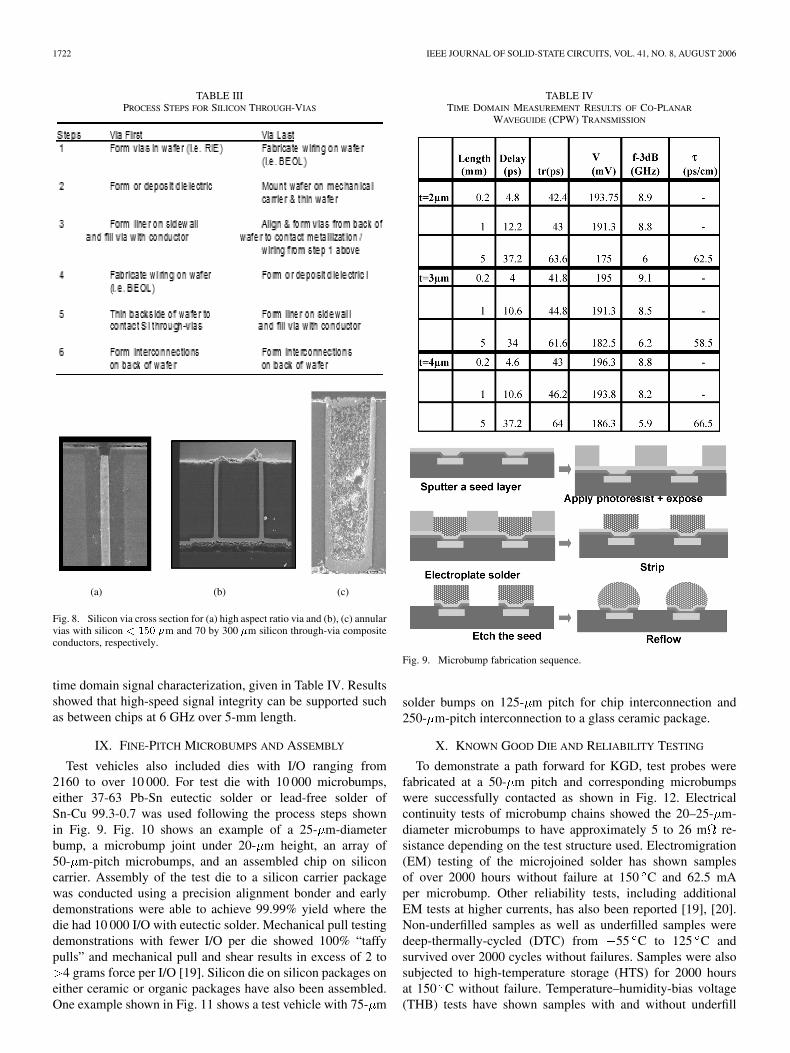
Fig. 6. Schematic cross section of silicon package supporting high-bandwidthchip-to-chip wiring (MMCM).
modeling. Portable product applications could achieve lowerpower operation and thus longer battery life.
V. MINI-MULTI-CHIP MODULES (MMCMS)
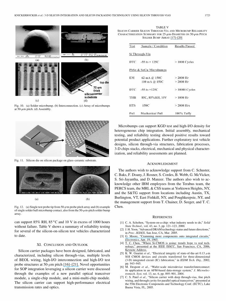
Fig. 6 shows a schematic cross section of a silicon carrierpackage which provides high-bandwidth chip interconnectionusing fine-pitch solder interconnection such as 50- m chip I/Opitch [16]–[20]. Fig. 7 shows a comparison of the relative band-width of silicon packaging compared to organic, ceramic, andprinted wiring board (PWB) per layer. Table II shows the corre-sponding parameter file. For chip-to-chip interconnection usinga silicon package over short distances such as 10 mm, band-width can be eight times the bandwidth of organic packagesand greater for comparison to ceramic or PWBs. Silicon carrierpackages that support these high I/O between die on a siliconcarrier packages may also benefit from reworkable solder in-terconnections and use of KGD. The high-bandwidth intercon-nection between die may provide new opportunities for hetero-geneous chip integration, opportunity to develop new architec-tures with microprocessor to memory chip stacks with reducedlatency and 2-D or 3-D structures with “virtual chip like” systembenefits.
VI. SILICON CHIP STACKING AND SILICON
PACKAGING TECHNOLOGY
Three-dimensional silicon-on-silicon stacks and silicon pack-ages have been fabricated as either thick free-standing silicon oras thin carriers which are under 150 m in thickness and requiremechanical support during processing or handling [16].
VII. SILICON THROUGH-VIA
A process sequence comparison for via formation in thin car-riers is shown in Table III. Here, the via process sequence is
Fig. 7. Bandwidth comparison for a silicon carrier package, ceramic, organic,and PWB [16].
TABLE IISUBSTRATE COMPARISON PARAMETERS [17]
compared for via first and via last processes. A more extensiveupdate on silicon through-vias has been reported [18].
Fig. 8 shows cross sections of silicon through-vias for 50- m-thick silicon and 300- m-thick silicon packages. A dielectric,liner, copper, and composite provide low coefficent of thermalexpansion for thermal excursions with deep vias for 300- m-thick silicon packages, whereas for thinner silicon packages,annular vias or high aspect ratio vias have been developed [17],[18]. In contrast, a handle wafer is used to support wafer pro-cessing and is later laser released or debonded for mthin silicon carriers where the thin silicon carrier is bonded toa supporting ceramic or organic structure. Free standing sil-icon packages and supported thin silicon carrier packages usedBEOL copper processing in addition to silicon through-vias toprovide for signal wiring, power and reference planes for re-ported electrical characterization.
VIII. FINE-PITCH WIRING
Coplanar waveguides have been fabricated, characterized,and modeled [16], [21]. Characterization included feature sizesranging from under one micron to several microns for linesand spaces. Signal integrity and voltage distribution modeling,simulation and measurement have been made where co-planarwaveguides, previously reported [7], [21], [22], were used for
1722 IEEE JOURNAL OF SOLID-STATE CIRCUITS, VOL. 41, NO. 8, AUGUST 2006
TABLE IIIPROCESS STEPS FOR SILICON THROUGH-VIAS
(a) (b) (c)
Fig. 8. Silicon via cross section for (a) high aspect ratio via and (b), (c) annularvias with silicon < 150 �m and 70 by 300 �m silicon through-via compositeconductors, respectively.
time domain signal characterization, given in Table IV. Resultsshowed that high-speed signal integrity can be supported suchas between chips at 6 GHz over 5-mm length.
IX. FINE-PITCH MICROBUMPS AND ASSEMBLY
Test vehicles also included dies with I/O ranging from2160 to over 10 000. For test die with 10 000 microbumps,either 37-63 Pb-Sn eutectic solder or lead-free solder ofSn-Cu 99.3-0.7 was used following the process steps shownin Fig. 9. Fig. 10 shows an example of a 25- m-diameterbump, a microbump joint under 20- m height, an array of50- m-pitch microbumps, and an assembled chip on siliconcarrier. Assembly of the test die to a silicon carrier packagewas conducted using a precision alignment bonder and earlydemonstrations were able to achieve 99.99% yield where thedie had 10 000 I/O with eutectic solder. Mechanical pull testingdemonstrations with fewer I/O per die showed 100% “taffypulls” and mechanical pull and shear results in excess of 2 to
4 grams force per I/O [19]. Silicon die on silicon packages oneither ceramic or organic packages have also been assembled.One example shown in Fig. 11 shows a test vehicle with 75- m
TABLE IVTIME DOMAIN MEASUREMENT RESULTS OF CO-PLANAR
WAVEGUIDE (CPW) TRANSMISSION
Fig. 9. Microbump fabrication sequence.
solder bumps on 125- m pitch for chip interconnection and250- m-pitch interconnection to a glass ceramic package.
X. KNOWN GOOD DIE AND RELIABILITY TESTING
To demonstrate a path forward for KGD, test probes werefabricated at a 50- m pitch and corresponding microbumpswere successfully contacted as shown in Fig. 12. Electricalcontinuity tests of microbump chains showed the 20–25- m-diameter microbumps to have approximately 5 to 26 m re-sistance depending on the test structure used. Electromigration(EM) testing of the microjoined solder has shown samplesof over 2000 hours without failure at 150 C and 62.5 mAper microbump. Other reliability tests, including additionalEM tests at higher currents, has also been reported [19], [20].Non-underfilled samples as well as underfilled samples weredeep-thermally-cycled (DTC) from 55 C to 125 C andsurvived over 2000 cycles without failures. Samples were alsosubjected to high-temperature storage (HTS) for 2000 hoursat 150 C without failure. Temperature–humidity-bias voltage(THB) tests have shown samples with and without underfill
KNICKERBOCKER et al.: 3-D SILICON INTEGRATION AND SILICON PACKAGING TECHNOLOGY USING SILICON THROUGH-VIAS 1723
Fig. 10. (a) Solder microbump. (b) Interconnection. (c) Array of microbumpsat 50-�m pitch. (d) Assembly.
Fig. 11. Silicon die on silicon package on glass–ceramic substrate.
(a) (b)
Fig. 12. (a) Single test probe tip from 50-�m probe pitch array and (b) exampleof single solder ball microbump contact, also from the 50-�m-pitch solder bumparray.
can support 85% RH, 85 C and 10 V in excess of 1000 hourswithout failure. Table V shows a summary of reliability testingfor several of the silicon-on-silicon test vehicles characterizedto date.
XI. CONCLUSION AND OUTLOOK
Silicon carrier packages have been designed, fabricated, andcharacterized, including silicon through-vias, multiple levelsof BEOL wiring, high-I/O interconnection and high-I/O testprobe structures at 50- m pitch [16]–[21]. Novel opportunitiesfor SOP integration leveraging a silicon carrier were discussedthrough the examples of a new parallel optical tranceivermodule, a single-chip module, and a mini-multi-chip module.The silicon carrier can support high-performance electricaltransmission rates and optics.
TABLE VSILICON CARRIER SILICON THROUGH-VIA AND MICROBUMP RELIABILITY
CHARACTERIZATION SUMMARY FOR 25-�m-DIAMETER ON 50-�m PITCH
SOLDER BUMP ARRAY [17]–[20]
Microbumps can support KGD test and high-I/O density forheterogeneous chip integration. Initial assembly, mechanicaltesting, and reliability testing showed positive results towardpotential product applications. Further exploratory test vehicledesigns, silicon through-via structures, fabrication processes,3-D chips stacks, electrical, mechanical and physical character-ization, and reliability assessments are planned.
ACKNOWLEDGMENT
The authors wish to acknowledge support from C. Schuster,C. Baks, F. Doany, J. Rosner, S. Cordes, B. Webb, G. McVicker,S. Sri-Jayantha, and D. Manzer. The authors also wish to ac-knowledge other IBM employees from the Terabus team, thePERCS team, the MRL & CSS teams at Yorktown Heights, NY,and the S&TG support from locations including Austin, TX,Burlington, VT, East Fishkill, NY, and Poughkeepsie, NY, andthe management support from T. Chainer, D. Seeger, and T. C.Chen.
REFERENCES
[1] C. A. Scholten, “System-on-a-chip: what industry needs to do,” SolidState Technol., vol. 43, no. 3, pp. 121–123, 2000.
[2] J. H. Yoon, “Advanced DRAM technology status and future directions,”in Proc. JEDEX, San Jose, CA, Mar. 2005.
[3] G. Moore, “Cramming more components onto integrated circuits,”Electronics, Apr. 19, 1965.
[4] T. C. Chen, “Where Si-CMOS is going: trendy hype vs real tech-nology,” presented at the IEEE ISSCC, San Francisco, CA, 2006,Keynote Address.
[5] K. W. Guarini et al., “Electrical integrity of state-of-the-art 0.13 �mSOI CMOS devices and circuits transferred for three-dimensional(3-D) integrated circuit (IC) fabrication,” in IEDM Tech. Dig., 2002,pp. 943–945.
[6] M. Despont et al., “Wafer-scale microdevice transfer/interconnect:its application in an AFM-based data-storage system,” J. Microelec-tromech. Syst, vol. 13, no. 6, pp. 895–901, 2004.
[7] C. S. Patel et al., “Silicon carrier with deep through-vias, fine pitchwiring, and through cavity for parallel optical transceiver,” presented atthe 55th Electronic Components and Technology Conf. (ECTC), LakeBuena Vista, FL, 2005.
1724 IEEE JOURNAL OF SOLID-STATE CIRCUITS, VOL. 41, NO. 8, AUGUST 2006
[8] A. W. Topol, “ Enabling SOI-based assembly technology for three-dimensional (3d) integrated circuits (ICs),” in IEDM Tech. Dig., 2005,pp. 352–355.
[9] E. D. Perfecto et al., “Thin-film multichip module packages forhigh-end IBM servers,” IBM J. Res. Develop., vol. 42, no. 5, pp.597–606, 1998.
[10] J. U. Knickerbocker et al., “An advanced multichip module (MCM) forhigh-performance UNIX servers,” IBM J. Res. Develop., vol. 46, no. 6,2002.
[11] K. Takahaski et al., ASET (Japan), “Process integration of 3-D chipstack with vertical interconnection,” presented at the 54th ElectronicComponents and Technology Conf. (ECTC), Las Vegas, NV, 2004.
[12] M. Feil et al., “The challenge of ultra thin chip assembly,” presented atthe 54th Electronic Components and Technology Conf. (ECTC), LasVegas, NV, 2004.
[13] M. Hunter et al., “Assembly and reliability of flip chip solder jointsusing miniaturized Au/Sn bumps,” presented at the 54th ElectronicComponents and Technology Conf. (ECTC), Las Vegas, NV, 2004.
[14] V. Kripesh et al., “Three-dimensional system-in-package using stackedsilicon platform technology,” IEEE Trans. Adv. Packag., vol. 28, no. 3,pp. 377–386, Aug. 2005.
[15] M. Umemoto et al., ASET (Japan), “High-performance vertical inter-connection for high-density 3D chip stacking package,” presented atthe 54th Electronic Components and Technology Conf. (ECTC), LasVegas, NV, 2004.
[16] J. U. Knickerbocker et al., “Development of next-generationsystem-on-package (SOP) technology based on silicon carrierswith fine pitch chip interconnection,” IBM J. Res. Develop., vol. 49,no. 4/5, pp. 725–753, 2005.
[17] J. U. Knickerbocker et al., “System-on-package (SOP) technology,characterization and applications,” presented at the 56th ElectronicComponents and Technology Conf. (ECTC), San Diego, CA, 2006.
[18] P. Andry et al., “A CMOS-compatible process for fabricating electricalthrough-vias in silicon,” presented at the 56th Electronic Componentsand Technology Conf. (ECTC), San Diego, CA, 2006.
[19] H. Gan et al., “Pb-free micro-joints for the next generation micro-systems: the fabrication, assembly and characterization,” presented atthe 56th Electronic Components and Technology Conf. (ECTC), SanDiego, CA, 2006.
[20] S. L. Wright et al., “Characterization of micro-bump C4 interconnectsfor Si-Carrier SOP applications,” presented at the 56th Electronic Com-ponents and Technology Conf. (ECTC), San Diego, CA, 2006.
[21] C. S. Patel, IBM Internal Communication and Reports. IBM T. J.Watson Research, Yorktown Heights, NY, 2005–2006.
[22] A. Deutsch et al., “Frequency-dependent losses on high-performanceinterconnections,” IEEE Trans. Electromagn. Compat., vol. 43, no. 4,pp. 446–465, Nov. 2001.
John U. Knickerbocker (M’06) received the B.S.and M.S. degrees in ceramic engineering from theState University of New York at Alfred, and the Ph.D.degree in ceramic engineering from the University ofIllinois at Urbana-Champaign.
He is currently an IBM Distinguished Engineerand the manager of the System-on-Package (SOP)Group. In 1983, he joined the IBM facility at EastFishkill, NY, where he held a series of engineeringand management positions, including Director ofIBM worldwide packaging development, manager
of package lead reduction and packaging strategist. In 2003, he joined the IBMResearch Division, Yorktown Heights, NY, where he has led the developmentof next-generation silicon carrier packaging and integration. He has authoredor coauthored 130 patents or patent applications and more than 26 papers andpublications.
Dr. Knickerbocker has received an IBM Corporate Award and three DivisionAwards, including IBM Outstanding Achievement Awards, three IBM PatentPortfolio Award Awards, and 30 Invention achievement awards. He serves as amember of the SEMATECH 3-D working group and has served on the technicaladvisory boards of multiple universities. He is a member of IMAPS and a Fellowof the American Ceramic Society.
Chirag S. Patel (M’03) received B.S., M.S. and PhD degrees in electrical en-gineering from the Georgia Institute of Technology, Atlanta, in 1995, 1996, and2001, respectively.
He is currently a Research Staff Member in the Science and Technology De-partment at the IBM Thomas J. Watson Research Center, Yorktown Heights,
NY. He joined the IBM Research Division in 2001, where he has worked onadvanced and exploratory packaging technologies. He is an author or coauthorof more than 35 technical papers.
Paul S. Andry received the B.Sc. degree in physicsfrom the University of Waterloo, ON, Canada,in 1986, the M.Sc. degree in physics from theUniversité de Sherbrooke, QC, Canada, in 1990,and the Ph.D. degree in materials science from theUniversity of Vermont, Burlington, in 1997.
He is currently a Research Staff Member atthe IBM T. J. Watson Research Center, YorktownHeights, NY. He joined IBM in 1997, working inthe Advanced Display Technology Laboratory on avariety of projects including prototypes of world’s
highest information content display, as well as the world’s first a-Si drivenOLED display. After serving as Technical Assistant to the VP of Science andTechnology, he returned to technical work in the System on Package Groupwhere he has been working on development of key technology elements andapplications of silicon carrier technology. He is a coeditor of the book ThinFilm Transistors (Marcell-Dekker, 2003), author or coauthor of more than 20professional publications, and holder of 20 issued or pending patents.
Cornelia K. Tsang received the B.S. and M.S. de-grees in materials science and engineering from theMassachusetts Institute of Technology, Cambridge,in 2000 and 2001, respectively.
She joined the IBM Research Division, YorktownHeights, NY, in 2001 and has worked since then inthe System-on-Package Group on novel process de-velopment and integration of silicon carrier packages.
L. Paivikki Buchwalter received her Diploma En-gineer (M.Sc. equivalent) and Doctor of Technologydegrees, both in chemical engineering, from HelsinkiUniversity of Technology, Finland in 1976 and 1997,respectively.
She is a Senior Scientist in the System-on-PackageGroup at the IBM Thomas J. Watson ResearchCenter, Yorktown Heights, NY. She joined IBMin 1980 at the IBM East Fishkill facility in thePolymer Science and Technology Group, movingto the Research Division in 1990. The bulk of her
professional career has focused on adhesion and related fields as they pertainto microelectronics conductor/insulator interfaces, in particular the adhesionof polyimide to inorganic surfaces. Throughout her 25 years at IBM, she hasworked on many interesting and diverse projects ranging from Cu/PI chipback-end-of-line processes to the application of MEMS to wireless communi-cation. More recently she has been working to develop processes related to Sicarrier build including Si through-vias, lamination, laser release, C4 joining,and under fill.
Dr. Buchwalter has received an IBM Research Division Award, an IBM Out-standing Technical Achievement Award, and several IBM Patent Awards. Sheholds 11 patents and is a Master Inventor.
Edmund J. Sprogis received the B.S.E.E. degreefrom Worcester Polytechnic Institute, Worcester,MA, in 1978, and the M.S.E.E. degree from theUniversity of Vermont, Burlington, in 1982.
He joined IBM, Essex Junction, VT, in 1978, andis currently a Senior Engineer in the Systems andTechnology Group, developing advanced 3-D semi-conductor packaging technology and applications.
KNICKERBOCKER et al.: 3-D SILICON INTEGRATION AND SILICON PACKAGING TECHNOLOGY USING SILICON THROUGH-VIAS 1725
Hua Gan received the B.S., M.S., and Ph.D. degrees in materials science andengineering from Southeast University, China, Northeastern University, Boston,MA, and the University of California at Los Angeles, respectively.
Following her study in electromigration and reliability in microelectronic in-terconnections, she joined IBM T. J Watson Center in 2004 as a post-doctorate,focusing on micro-joint development and reliability for silicon-on-packageproject. In 2005, she joined the IBM System And Technology Group, HopewellJunction, NY, as an Advisory Engineer, working on C4 interconnects develop-ment. She is an author or coauthor of more than 15 technical papers.
Dr. Gan is a member of the Material Research Society.
Raymond R. Horton is a Staff Engineer at theIBM Thomas J. Watson Research Center, York-town Heights, NY, where he is a member of theSystem-on-Package Group and is responsible forbonding, assembly, and testing of interconnections.His work experience includes at-panel displayassembly and test and packaging. He is a coauthorof numerous technical publications and patents.
Mr. Horton has received an IBM OutstandingTechnical Achievement Award.
Robert J. Polastre received the Associate degree inelectronic technology and the Bachelor’s degree fromLaSalle University, Philadelphia, PA.
He joined the IBM Research Division, YorktownHeights, NY, in 1983. He is currently a Staff Engi-neer working in the System-on-Package Group. He isthe author or coauthor of several papers on automatedand thermal testing and is a coinventor of patents inthese areas.
Mr. Polastre received IBM Outstanding TechnicalAchievement Awards in 1990 and 1999 and an IBM
Corporate Award in 1993 for his work on array testing of thin-film transistors.
Steven L. Wright did graduate student work in elec-trical engineering at the University of Colorado andthe University of California at Santa Barbara.
He joined IBM in 1982 as a Research StaffMember. During his career at IBM, he has workedin four areas: materials science and device physicsof III-V compound heterojunctions, liquid-crystalflat-panel display technology, development andmarketing of high-resolution visualization tech-nology and products, and silicon carrier packagingtechnology. He is currently a member of the
System-on-Package Group in the Department of Electronic and OpticalPackaging, IBM Thomas J. Watson Research Center, Yorktown Heights, NY,focusing on test and reliability issues for silicon carrier technology. He hascontributed to more than 150 publications.
Dr. Wright has received six IBM Invention Achievement Awards and threeIBM Research Division Awards.
John M. Cotte received the B.S. degree in chemicalengineering from Bucknell University, Lewisburg,PA, in 1984, and the M.S. degree in materials scienceand engineering from the University of Pittsburgh,Pittsburgh, PA, in 1988.
He is an Advisory Engineer at the IBM Thomas J.Watson Research CenterYorktown Heights, NY. Hejoined the IBM Research Division in 1988 and hasworked in the Physical Sciences, Manufacturing Re-search, Silicon Technology and Electronic and Op-tical Packaging organizations. He has extensive expe-
rience in surface analysis and materials characterization, as well as unit processdevelopment in the areas of backend interconnects and chip packaging. Cur-rently, he is working on novel processes to fabricate and integrate rf MEMSfor communication applications, and through-via fabrication for 3-D integra-tion and silicon packaging. He holds 39 U.S. patents
Mr. Cotte has received 15 IBM Invention Achievement Awards.
Related Documents