EC6302 DIGITAL ELECTRONICS L T P C 3 0 0 3 OBJECTIVES: To introduce basic postulates of Boolean algebra and shows the correlation between Boolean expressions To introduce the methods for simplifying Boolean expressions To outline the formal procedures for the analysis and design of combinational circuits and sequential circuits To introduce the concept of memories and programmable logic devices. To illustrate the concept of synchronous and asynchronous sequential circuits UNIT I MINIMIZATION TECHNIQUES AND LOGIC GATES 9 Minimization Techniques: Boolean postulates and laws – De-Morgan‟s Theorem - Principle of Duality - Boolean expression - Minimization of Boolean expressions –– Minterm - Maxterm - Sum of Products (SOP) – Product of Sums (POS) – Karnaugh map Minimization – Don‟t care conditions – Quine - McCluskey method of minimization. Logic Gates: AND, OR, NOT, NAND, NOR, Exclusive–OR and Exclusive–NOR Implementations of Logic Functions using gates, NAND–NOR implementations – Multi level gate implementations- Multi output gate implementations. TTL and CMOS Logic and their characteristics – Tristate gates UNIT II COMBINATIONAL CIRCUITS 9 Design procedure – Half adder – Full Adder – Half subtractor – Full subtractor – Parallel binary adder, parallel binary Subtractor – Fast Adder - Carry Look Ahead adder – Serial Adder/ Subtractor - BCD adder – Binary Multiplier – Binary Divider - Multiplexer/ Demultiplexer – decoder - encoder – parity checker – parity generators – code converters – Magnitude Comparator. UNIT III SEQUENTIAL CIRCUITS 9 Latches, Flip-flops - SR, JK, D, T, and Master-Slave – Characteristic table and equation – Application table – Edge triggering – Level Triggering – Realization of one flip flop using other flip flops – serial adder/subtractor- Asynchronous Ripple or serial counter – Asynchronous Up/Down counter - Synchronous counters – Synchronous Up/Down counters – Programmable counters – Design of Synchronous counters: state diagram- State table – State minimization – State assignment - Excitation table and maps-Circuit implementation - Modulo–n counter, Registers – shift registers - Universal shift registers – Shift register counters – Ring counter – Shift counters - Sequence generators. UNIT IV MEMORY DEVICES 9 Classification of memories – ROM - ROM organization - PROM – EPROM – EEPROM – EAPROM, RAM – RAM organization – Write operation – Read operation – Memory cycle - Timing wave forms – Memory decoding – memory expansion – Static RAM Cell- Bipolar RAM cell – MOSFET RAM cell – Dynamic RAM cell –Programmable Logic Devices – Programmable Logic Array (PLA) - Programmable Array Logic (PAL) – Field Programmable Gate Arrays (FPGA) - Implementation of combinational logic circuits using ROM, PLA, PAL.

Welcome message from author
This document is posted to help you gain knowledge. Please leave a comment to let me know what you think about it! Share it to your friends and learn new things together.
Transcript

EC6302 DIGITAL ELECTRONICS L T P C
3 0 0 3
OBJECTIVES:
To introduce basic postulates of Boolean algebra and shows the correlation between
Boolean expressions
To introduce the methods for simplifying Boolean expressions
To outline the formal procedures for the analysis and design of combinational circuits
and sequential circuits
To introduce the concept of memories and programmable logic devices.
To illustrate the concept of synchronous and asynchronous sequential circuits
UNIT I MINIMIZATION TECHNIQUES AND LOGIC GATES 9
Minimization Techniques: Boolean postulates and laws – De-Morgan‟s Theorem - Principle
of Duality - Boolean expression - Minimization of Boolean expressions –– Minterm -
Maxterm - Sum of Products (SOP) – Product of Sums (POS) – Karnaugh map Minimization
– Don‟t care conditions – Quine - McCluskey method of minimization.
Logic Gates: AND, OR, NOT, NAND, NOR, Exclusive–OR and Exclusive–NOR
Implementations of Logic Functions using gates, NAND–NOR implementations – Multi
level gate implementations- Multi output gate implementations. TTL and CMOS Logic and
their characteristics – Tristate gates
UNIT II COMBINATIONAL CIRCUITS 9
Design procedure – Half adder – Full Adder – Half subtractor – Full subtractor – Parallel
binary adder, parallel binary Subtractor – Fast Adder - Carry Look Ahead adder – Serial
Adder/ Subtractor - BCD adder – Binary Multiplier – Binary Divider - Multiplexer/
Demultiplexer – decoder - encoder – parity checker – parity generators – code converters –
Magnitude Comparator.
UNIT III SEQUENTIAL CIRCUITS 9
Latches, Flip-flops - SR, JK, D, T, and Master-Slave – Characteristic table and equation –
Application table – Edge triggering – Level Triggering – Realization of one flip flop using
other flip flops – serial adder/subtractor- Asynchronous Ripple or serial counter –
Asynchronous Up/Down counter - Synchronous counters – Synchronous Up/Down counters
– Programmable counters – Design of Synchronous counters: state diagram- State table –
State minimization – State assignment - Excitation table and maps-Circuit implementation -
Modulo–n counter, Registers – shift registers - Universal shift registers – Shift register
counters – Ring counter – Shift counters - Sequence generators.
UNIT IV MEMORY DEVICES 9
Classification of memories – ROM - ROM organization - PROM – EPROM – EEPROM –
EAPROM, RAM – RAM organization – Write operation – Read operation – Memory cycle -
Timing wave forms – Memory decoding – memory expansion – Static RAM Cell- Bipolar
RAM cell – MOSFET RAM cell – Dynamic RAM cell –Programmable Logic Devices –
Programmable Logic Array (PLA) - Programmable Array Logic (PAL) – Field
Programmable Gate Arrays (FPGA) - Implementation of combinational logic circuits using
ROM, PLA, PAL.

UNIT V SYNCHRONOUS AND ASYNCHRONOUS SEQUENTIAL CIRCUITS 9
Synchronous Sequential Circuits: General Model – Classification – Design – Use of
Algorithmic State Machine – Analysis of Synchronous Sequential Circuits
Asynchronous Sequential Circuits: Design of fundamental mode and pulse mode circuits –
Incompletely specified State Machines – Problems in Asynchronous Circuits – Design of
Hazard Free Switching circuits. Design of Combinational and Sequential circuits using
VERILOG.
TOTAL: 45 PERIODS
OUTCOMES: Students will be able to:
Analyze different methods used for simplification of Boolean expressions.
Design and implement Combinational circuits.
Design and implement synchronous and asynchronous sequential circuits.
Write simple HDL codes for the circuits.
TEXT BOOK:
1. M. Morris Mano, “Digital Design”, 4th Edition, Prentice Hall of India Pvt. Ltd., 2008 /
Pearson Education (Singapore) Pvt. Ltd., New Delhi, 2003.
REFERENCES:
1. John F.Wakerly, “Digital Design”, Fourth Edition, Pearson/PHI, 2008
2. John.M Yarbrough, “Digital Logic Applications and Design”, Thomson Learning, 2006.
3. Charles H.Roth. “Fundamentals of Logic Design”, 6th Edition, Thomson Learning, 2013.
4. Donald P.Leach and Albert Paul Malvino, “Digital Principles and Applications”, 6th
Edition, TMH,2006.

LIST OF TABLE CONTENTS
Unit
No Name of the Content
Page
No
1 MINIMIZATION TECHNIQUES AND LOGIC GATES 1
1.1 Boolean postulates and laws 1
1.2 De-Morgan’s Theorem 2
1.2.1 Application of Demorgan's theorems 3
1.3 Principle of Duality 4
1.4 Boolean expression 4
1.5Minimization of Boolean Expressions 4
1.6 Sum-of-Products (SOP) Form 5
1.6.1 Canonical Form 5
1.6.2 MINTERM ( Canonical SOP) 5
1.6.3 MAXTERM (Canonical POS) 6
1.7 Standard Sop Form & Minterms 8
1.7.1 Characteristics of A Minterm 8
1.8 Product-of-Sums (POS) Form 9
1.8.1 Product-of-Sums (POS) Form 9
1.8.2 Implementation of POS Expression 9
1.9 Standard POS Form & Maxterms 10
1.9.1 Standard POS Form 10
1.9.2 Characteristics of a Maxterm 10
1.10 Keeping Circuits Simple (Karnaugh Maps) 11
1.10.1Three Variable Karnaughmap 12
1.10.2 Map From 4 Variables Truth Table or SOP Form Boolean
Expression 16
1.10.3 Five Variable Karnaugh Map 19
1.11Quine-Mccluskey (Tabular) Minimization 20
1.12logic Gates 27
1.13 NAND–NOR Implementations 33
1.14 TTL Family of ICS 38
1.15 CMOS Family of ICS 40
1.16 Tristate Gates 40
2 COMBINATIONAL CIRCUITS 42
2.1 Half Adder 42
2.2 Full-Adder 42
2.2.1 Full Adder Circuit Using And-Or 44
2.2.2 Full Adder Circuit Using Xor 44
2.3 Subtractor 44
2.3.1 Half Subtractor 45
2.3.2 Full Subtractor 46
2.4-Bit Binary Parallel Adder And Subtractor 48
2.5 Carry Propagation and The Look-Ahead Carry Circuit 49
2.6 Serial Adder With Accumulator 51
2.7 Serial Subtractor 52
2.8 BCD Adder 53

2.9 Cascading BCD Adders 54
2.10 Binary Multiplier 55
2.10.1 2-Bit By 2-Bit Binary Multiplier 56
2.11 Multiplexer 57
2.12 De-Multiplexers 61
2.13 Encoders 62
2.14 Decoders 63
2.15 Parity Generator And Checker: 66
2.16 Code Converters 68
2.17 Comparator 70
3 SEQUENTIAL CIRCUITS 73
3.1.Sr Flip-Flop 73
3.1.1the Nand Gate SR Flip-Flop 73
3.1.2 Switch Debounce Circuits 75
3.1.3gated Or Clocked SR Flip-Flop 76
3.1.4 Edge-Triggered SR Flip-Flops 77
3.2.D Flipflop 78
3.3 JK Flip-Flops 80
3.4.Master-Slave Flip-Flops 81
3.4.1 Level-Triggered SR Flip-Flop 81
3.4.2 Ripple Counter (Asynchronous Counter) 82
3.5 Synchronous Counter 84
3.5.1synchronous Up /Down Counter 85
3.6 Asynchronous Up /Down Counter 86
3.6.1 Design Of Synchronous Counters 87
3.7.The Shift Register 94
3.7.1.Serial-In To Parallel-Out 96
3.7.2 Serial-In To Serial-Out 97
3.7.3 Parallel-In To Serial-Out (PISO) 98
3.7.4 Parallel-In To Parallel-Out (PIPO) 98
3.8 Universal Shift Register 99
3.9.The Ring Counter 100
3.10 Johnson Ring Counter 102
4 MEMORY DEVICES 105
4.1. Classifications of Memory 105
4.2 Types of RAM 105
4.3. Types of Rom 105
4.4 Hybrid Types 106
4.5. Programmable Logic Devices 108
4.6 Programmable Logic Devices 108
4.7 Fixed Logic Versus Programmable Logic 109
4.8 Programmable Logic Devices 111
4.8.1 Programmable ROMs 111
4.8.2 Programmable Logic Array 112
4.8.3 Complex Programmable Logic Device 113
4.8.4 Field-Programmable Gate Array 113
4.9Memory Hierarchy 114
4.10Random-Access Memory (RAM) 116

4.11 Memory Details 118
5 SYNCHRONOUS AND ASYNCHRONOUS SEQUENTIAL
CIRCUITS
119
5.1 Introduction 119
5.2 Synchronous Sequential Circuit 119
5.3 Concept of Sequential Logic 120
5.3.1 Level Sensitive 121
5.3.2 Edge Sensitive 122
5.4 Latches and Flip-Flops 123
5.4.1 RS Latch 124
5.4.2 RS Latch with Clock 124
5.4.2.1 Set up and Hold time 125
5.4.3 D Latch 125
5.4.4 JK Latch 126
5.4.5 T Latch 127
5.4.6 JK Master Slave Flip-Flop 128
5.5 Sequential Circuits Design Procedures 128
5.5.1 State Diagram 129
5.5.2 State Table 129
5.5.3 K-map 129
5.5.4 Circuit 130
5.6 Sequential Circuits Analysis Procedures 130
5.6.1 State Equations 130
5.6.2 State Table 132
5.6.3 State Diagram 132
5.6.4 Flip-Flop Input Equations 133
5.7 Analysis With D Flip-Flops 134
5.8 Analysis With Jk Flip-Flops 135
5.9 Analysis With T Flip-Flops 137
5.10 Mealy And Moore Models 139
5.11 State Reduction & Assignment 140
5.12 Shift Registers 142
5.12.1 Introduction 142
5.12.2 Serial In - Serial Out Shift Registers 143
5.12.3 Serial In - Parallel Out Shift Registers 143
5.12.4 Parallel In - Serial Out Shift Registers 144
5.12.5 Parallel In - Parallel Out Shift Registers 144
5.13 Counters 145
5.13.1 Benefits of counters 145
5.13.2 Design Example: Synchronous BCD Counter 145
5.13.3 Counter Types 146
5.14 HDL For Sequential Circuits 146
5.14.1 Behavioral Modeling 146
5.14.2 Descriptions of Circuits 147
5.14.3 Flip-Flops and Latches 147
5.15 Asynchronous Sequential Circuits – Introduction 148
5.16 Analysis Procedure 149
5.16.1 Transition Table 149
5.17 Flow Table 151
5.17.1 Race Conditions 151
5.17.2 Analysis Example 153
5.17.3 Design Procedure 154
5.17.4 Design Example – Specification 154
5.17.5 Reduction of State and Flow Tables 158
5.17.6 Implication Table 158
5.17.7 Merging of the Flow Table 160
5.17.8 Compatible Pairs 161
5.17.9 Maximal Compatibles 161
5.18 Race-Free State Assignment 162
5.19 Three-Row Flow Table Example 162
5.20 Four-Row Flow Table Example 163
5.21Hazards 164
5.22 Hazards in Combinational Circuits 165
5.23 Hazards in Sequential Circuits 167
5.24 Essential Hazards 167
5.25 ASM Chart 167
5.27.1 The ASM Block Diagram 168
5.27.2 Certain Rules 168
5.27.3 Parallel vs. Serial 169
5.27.4 Sequence Detector Example 169
5.27.5 Event Tables 170
5.27.6 Asynchronous and Synchronous Output Example 170
5.27.7 Clock Enable 171
Unit 1 Part A Question with Answer 172
Unit 2 Part A Question with Answer 178
Unit 3 Part A Question with Answer 184
Unit 4 Part A Question with Answer 188
Unit 5 Part A Question with Answer 192
Question bank with unit wise 195

EC6302 DIGITAL ELECTRONICS
SCE 1 ECE
UNIT 1-MINIMIZATION TECHNIQUES AND LOGIC GATES
1.1 BOOLEAN POSTULATES AND LAWS:
T1 : Commutative Law
(a) A + B = B + A
(b) A B = B A
T2 : Associate Law (a) (A + B) + C = A + (B + C)
(b) (A B) C = A (B C)
T3 : Distributive Law
(a) A (B + C) = A B + A C
(b) A + (B C) = (A + B) (A + C)
T4 : Identity Law (a) A + A = A
(b) A A = A
T5 :
(a)
(b)
T6 : Redundance Law
(a) A + A B = A
(b) A (A + B) = A
T7 : (a) 0 + A = A
(b) 0 A = 0
T8 :
(a) 1 + A = 1
(b) 1 A = A
T9 :
(a)
(b)
T10 :
(a)
(b)
Boolean Theorems
Investigating the various Boolean theorems (rules) can help us to simplify logic
expressions and logic circuits.

EC6302 DIGITAL ELECTRONICS
SCE 2 ECE
Boolean postulates are
— The Commutative Law of addition for two variable.
A + B = B +
A
— The Commutative Law of multiplication for two variable.
A . B = B
. A
— The Associative law of addition with multiplication is written as
A + (B + C) = A +B +C
— The Associative law of multiplication with addition is written as
A . (B
. C) = (A
. B)
. C
— The Associative law of multiplication with addition is written as
A . (B + C) = A
. B + A
. C
— The Associative law of addition with multiplication is written as
A + (B . C) = (A + B) . (A + C)
(1) A + 0 = A A · 1 = A identity
(2) A + [A] ' = 1 A · [A] ' = 0 complement
(3) A + B = B + A A · B = B · A commutative law
(4) A + (B + C) = (A + B) + C A · (B · C) = (A · B) · C associative law
(5) A + (B · C) = (A + B) · (A + C) A · (B + C) = (A · B) + (A ·
C) distributive law
(6) A + A = A A · A = A
(7) A + 1 = 1 A · 0 = 0
(8) A + (A · B) = A A · ( A + B) = A
(9) A + ([A] ' · B) = A + B A · ([A] ' + B) = A · B
(10) A + (B . C) = (A + B) . (A + C) A · (B + C) = (A · B) + (A ·
C)
(11) [A + B] ' = [A] ' · [B] ' [A · B] ' = [A] ' + [B] ' de Morgan's
theorem

EC6302 DIGITAL ELECTRONICS
SCE 3 ECE
1.2 DE-MORGAN’S THEOREM:
De Morgan suggested two theorems that form important part of Boolean algebra.
They are,
1) The complement of a product is equal to the sum of the complements.
(AB)' = A' + B'
• FIRST THEOREM
2) The complement of a sum term is equal to the product of the complements.
(A + B)' = A'B'
• SECOND THEOREM
1.2.1 APPLICATION OF DEMORGAN'S THEOREMS:
BABA .
A
BB.A
A
B
BA
BABA .
A
BBA
A
B
B.A

EC6302 DIGITAL ELECTRONICS
SCE 4 ECE
Apply to any number of variables:
Apply to combination of variables:
1.3 PRINCIPLE OF DUALITY:
Principle of Duality theorem says,
Changing each OR sign to an AND sign
Changing each AND sign to an OR sign
Complementing any 0 or 1 appearing in the expression
1.4 BOOLEAN EXPRESSION:
Boolean expressions are minimized by using Boolean laws and postulates.
1.5 MINIMIZATION OF BOOLEAN EXPRESSIONS
Simplify the Boolean expression F=x′y′z′+x′yz+xy′z′+xyz′
Given
F=x′y′z′+x′yz+xy′z′+xyz′
=x′y′z′+x′yz+xz′(y′+y)
=x′y′z′+x′yz+xz′
=x′yz+ z′(x′y′+x)
= x′yz+z′(x′+x)(y′+x)
F=x′yz+xz′+z′y′
– Sum-of-Products (SOP) Form
– Product-of-Sums (POS) Form
– Each form may contain single variable terms
– May contain complemented and un-complemented terms
– A SOP and POS expression can’t have a term of more than one variable having an
over bar extending over the entire term
• Sum-of-Product (SOP) form: When two or more product terms are summed by
Boolean addition, the result is a Sum-of-Product or SOP expression
• Product-of-Sum (POS) form: When two or more sum terms are multiplied by Boolean
multiplication, the result is a Product-of-Sum or POS expression
• The Domain of an SOP and POS expression is the set of variables contained in the
expression, both complemented and un-complemented.
• A SOP and POS expression can have a single variable term such as A
).().().).(.( BCACBABCACBA
BCACBA .).().(.
BCACBA ).().(
CBBACABA ....
CBCABA ...
ZYXZYX ..
Z.Y.XZYX

EC6302 DIGITAL ELECTRONICS
SCE 5 ECE
• A SOP and POS expression cannot have a term of more than one variable having an
over bar extending over the entire term.
1.6 SUM-OF-PRODUCTS (SOP) FORM:
Two or more product terms summed by Boolean addition
Any expression -> SOP using Boolean algebra
Example:
A + BC
Sum-of-Products (SOP) Form:
Implementation of SOP Expression by using basic gates
B+AC+AD
1.6.1 CANONICAL FORM:
In SOP and POS, if all the term contains all the variables either in true or in
complementary form then its said to be canonical SOP or canonical POS.
1.6.2 MINTERM ( canonical SOP)
In a Boolean function, a binary variable (x) may appear either in its normal form (x)
or in its complement form (x’).Consider 2 binary variables x and y and an AND operation,
there are 4 and only 4 possible combinations: x’•y’, x’•y, x•y’ & x•y.
Each of the 4 product terms is called a MINTERM or STANDARD PRODUCT
By definition, a Minterm is a product which consists of all the variables in the normal
form or the complement form but NOT BOTH.
e.g. for a function with 2 variables x and y:
x•y’ is a minterm but x’ is NOT a minterm
e.g. for a function with 3 variables x, y andz:
BEFBCDAB)EFCD(BAB*
BDBCBADACAB)DCB)(BA(*
BADAC
CBCAC)BA(C)BA(C)BA(*
A
B
C
B+AC+AD
A
D
EC6302 DIGITAL ELECTRONICS
SCE 6 ECE
x’yz’ is a minterm but xy’ is NOT a minterm
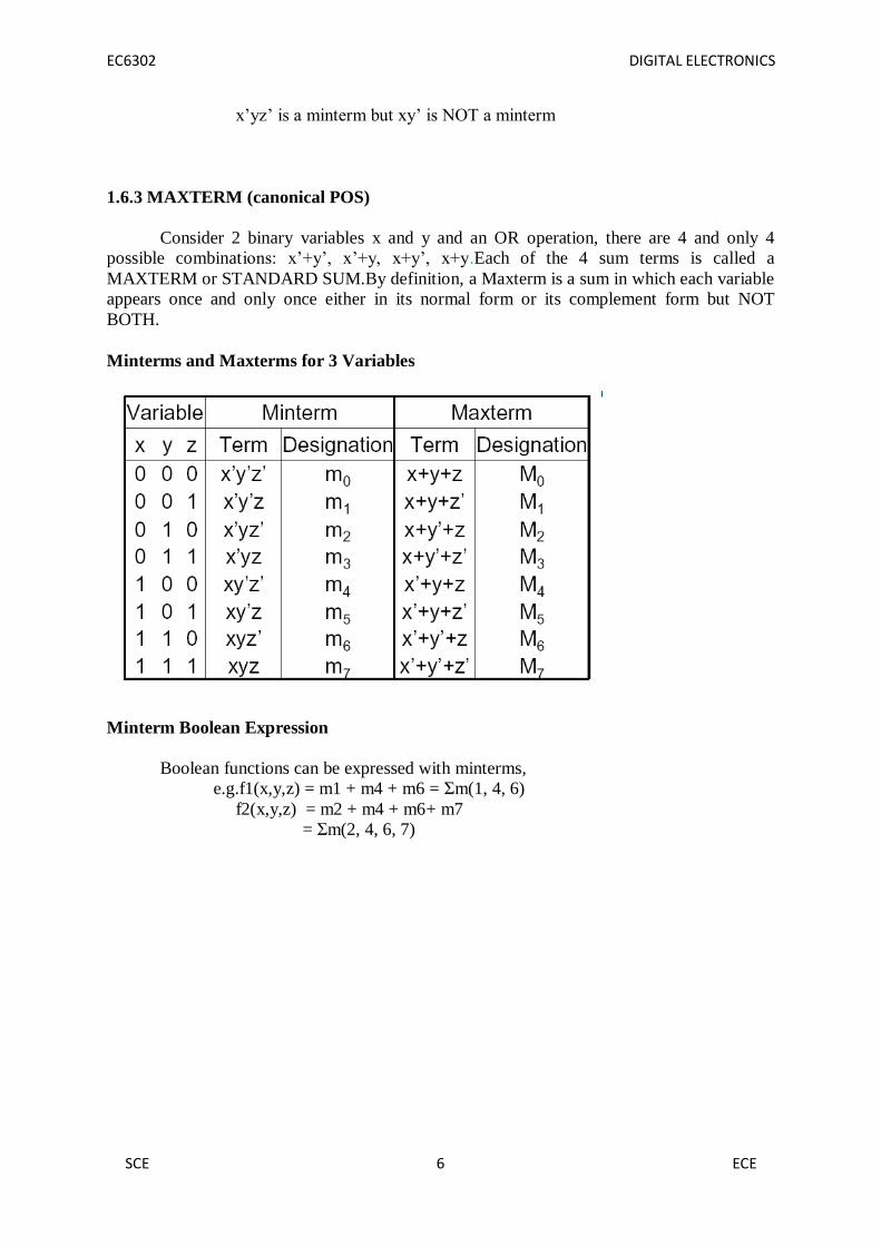
1.6.3 MAXTERM (canonical POS)
Consider 2 binary variables x and y and an OR operation, there are 4 and only 4
possible combinations: x’+y’, x’+y, x+y’, x+y.Each of the 4 sum terms is called a
MAXTERM or STANDARD SUM.By definition, a Maxterm is a sum in which each variable
appears once and only once either in its normal form or its complement form but NOT
BOTH.
Minterms and Maxterms for 3 Variables
Minterm Boolean Expression
Boolean functions can be expressed with minterms,
e.g.f1(x,y,z) = m1 + m4 + m6 = Σm(1, 4, 6)
f2(x,y,z) = m2 + m4 + m6+ m7
= Σm(2, 4, 6, 7)

EC6302 DIGITAL ELECTRONICS
SCE 7 ECE
Maxterm Boolean Expression
Boolean functions can also be expressed with maxterms,
e.g.f1’ = x’y’z’+x’yz’+x’yz+xy’z+xyz
f1 = (x’y’z’+x’yz’+x’yz+xy’z+xyz)’
= (x+y+z)(x+y’+z)(x+y’+z’)(x’+y+z’)(x’+y’+z’)
= M0•M2•M3•M5•M7
= Π M(0, 2, 3, 5, 7)
f2 = M0•M1•M3•M5
= Π M(0, 1, 3, 5)
Express Boolean Functions in Minterms
If product terms in a Boolean function are not minterms, they can be converted to minterms
e.g. f(a,b,c) = a’ + bc’ + ab’c
Function f has 3 variables, therefore, each minterm must have 3 literals.
Neither a’ nor bc’ are minterms.They can be converted to minterm.ab’c is a minterm
Conversion to Minterms
e.g. f(a,b,c) = a’ + bc’ + ab’c
To convert a’ to a minterm, the 2 variables (b, c) must be added, without changing its
functionality .Since a’=a’•1 & 1 = b+b’, a’= a’(b + b’) = a’b + a’b’
Similarly, a’b = a’b(c + c’) = a’bc + a’bc’ and a’b’ = a’b’(c+c’) = a’b’c + a’b’c’
bc’ = bc’(a+a’) = abc’ + a’bc’
EC6302 DIGITAL ELECTRONICS
SCE 8 ECE
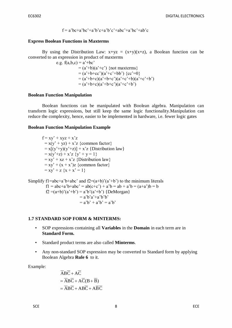
f = a’bc+a’bc’+a’b’c+a’b’c’+abc’+a’bc’+ab’c
Express Boolean Functions in Maxterms
By using the Distribution Law: x+yz = (x+y)(x+z), a Boolean function can be
converted to an expression in product of maxterms
e.g. f(a,b,c) = a’+bc’
= (a’+b)(a’+c’) {not maxterms}
= (a’+b+cc’)(a’+c’+bb’) {cc’=0}
= (a’+b+c)(a’+b+c’)(a’+c’+b)(a’+c’+b’)
= (a’+b+c)(a’+b+c’)(a’+c’+b’)
Boolean Function Manipulation
Boolean functions can be manipulated with Boolean algebra. Manipulation can
transform logic expressions, but still keep the same logic functionality.Manipulation can
reduce the complexity, hence, easier to be implemented in hardware, i.e. fewer logic gates
Boolean Function Manipulation Example
f = xy’ + xyz + x’z
= x(y’ + yz) + x’z {common factor}
= x[(y’+y)(y’+z)] + x’z {Distribution law}
= x(y’+z) + x’z {y’ + y = 1}
= xy’ + xz + x’z {Distribution law}
= xy’ + (x + x’)z {common factor}
= xy’ + z {x + x’ = 1}
Simplify f1=abc+a’b+abc’ and f2=(a+b)’(a’+b’) to the minimum literals
f1 = abc+a’b+abc’ = ab(c+c’) + a’b = ab + a’b = (a+a’)b = b
f2 =(a+b)’(a’+b’) = a’b’(a’+b’) {DeMorgan}
= a’b’a’+a’b’b’
= a’b’ + a’b’ = a’b’
1.7 STANDARD SOP FORM & MINTERMS:
• SOP expressions containing all Variables in the Domain in each term are in
Standard Form.
• Standard product terms are also called Minterms.
• Any non-standard SOP expression may be converted to Standard form by applying
Boolean Algebra Rule 6 to it.
Example:
CBACABCBA
)BB(CACBA
CACBA

EC6302 DIGITAL ELECTRONICS
SCE 9 ECE
Example: Determine Standard SOP expression
Introduce all possible combinations of the missing variables AND’ed with the original term
1.7.1 CHARACTERISTICS OF A MINTERM:
• Minterm is a standard product term in which all variables appear exactly once
(complemented or uncomplemented)
• Represents exactly one combination of the binary variables in a truth table for which
the function produces a “1” output. That is the binary representation or value.
• Has value of 1 for that combination and 0 for all others
• For n variables, there are 2n distinct minterms
Example:
Express the Boolean function F=A+B′C in sum of min terms.
Given
F=A+B′C
=A(B+ B′)(C+C′)+ B′C(A+A′)
=(AB+A B′)(C+C′)+B′C(A+A′)
=ABC+ABC′+AB′C+AB′C′+AB′C+A′B′C
= ABC+ABC′+AB′C+AB′C+A′B′C
F=m1+m4+m5+m6+m7
1.8 PRODUCT-OF-SUMS (POS) FORM:
• Two or more sum terms multiplied by Boolean multiplication
• Any expression -> POS using Boolean algebra
• Examples:
(A+B)(B+C)(A+B+C)
1.8.1 PRODUCT-OF-SUMS (POS) FORM:
• Conversion to POS Form:
CBACBACABABCCBA
)CBCBCBBC(ACBA
)CC)(BB(ACBA
ACBA
1010
DCBA
)DCA(B)DC(BAB*
)DB)(CB(A)CDB(AACDAB*
C)BA(C)BA(C)BA(*

EC6302 DIGITAL ELECTRONICS
SCE 10 ECE
1.8.2 IMPLEMENTATION OF POS EXPRESSION:
(A+B)(B+C+D)(A+C)
1.9 STANDARD POS FORM & MAXTERMS:
• POS expressions containing all Variables in the Domain in each term are in
Standard Form.
• Standard sum terms are also called Maxterms. A Maxterm is a NOT Minterm.
• Any non-standard POS expression may be converted to Standard form by applying
Boolean Algebra Rule 8 and Rule 12 A+BC=(A+B)(A+C) to it.
1.9.1 STANDARD POS FORM:
Example:
SHORTCUT: Introduce all possible combinations of the missing variables OR’ed with the
original term
1.9.2 CHARACTERISTICS OF A MAXTERM:
• Maxterm is a standard sum term in which all variables appear exactly once
(complemented or uncomplemented)
• Represents exactly one combination of the binary variables in a truth table for which
the function produces a “0” output. That is the binary representation or value.
• Has value of 0 for that combination and 1 for all others
• For n variables, there are 2n distinct maxterms
Example:
D
C
(A+B)(B+C+D)(A+C)
A
B
)CBA)(CBA)(CBA(
)BCA)(BCA)(CBA(
)BBCA)(CBA(
)CA)(CBA(
)1100(
)DCBA(

EC6302 DIGITAL ELECTRONICS
SCE 11 ECE
Why Standard SOP and POS Forms?
• Direct mapping of Standard Form expressions and Truth Table entries.
• Alternate Mapping methods for simplification of expressions
• Minimal Circuit implementation by switching between Standard SOP or POS
• PLD based function implementation
Express the Boolean function as
1) POS form
2) SOP form
D=(A′+B)(B′+C)
POS form:
Given
D=(A′+B)(B′+C)
=A′B′+A′C+BB′+BC
= A′B′+A′C+BC
= A′+B′+ A′C+BC
= A′(1+C)+B′+BC
= A′+B′+BC
D= A′B′+BC
Using missed terms formulae;
= A′B′(C+C′)+(A+A′)BC
= A′B′C+ A′B′C′+ABC+A′BC
D(A,B,C)= Σ m(1,0,7,3)
D= A′B′+BC
SOP form:
D(A,B,C)= πM(1,0,7,3)
D′=(A′+B′)(B+C)

EC6302 DIGITAL ELECTRONICS
SCE 12 ECE
1.10 KEEPING CIRCUITS SIMPLE (KARNAUGH MAPS)
We have just seen how using the logic identities can simplify a Boolean expression. This is
important because it reduces the number of gates needed to construct the logic circuit.
However, as I am sure you will agree, having to work out Boolean problems in longhand is
not easy. It takes time and ingenuity Here’s a basic outline showing how to apply Karnaugh
mapping to a three-input system:
1. First, select a desired truth table.
2. Next, translate the truth table into a Karnaugh map. AKarnaugh map is similar to a truth
table but has its variables represented along two axes. Translating the truth table into a
Karnaugh map reduces the number of 1s and 0s needed to present the information. Figure
shows how the translation is carried out.
3. After you create the Karnaugh map, you proceed to encircle adjacent cells of 1s into
groups of 2, 4, or 8. The more groups you can encircle, the simpler the final equation will
be. In other words, take all possible loops.
4. Now, identify the variables that remain constant within each loop, and write out an SOP
equation by ORing these variables together. Here, constant means that a variable and its
inverse are not present together within the loop. For example, the top horizontal loop in
Fig. yields A_B_ (the first term in the SOP expression), since A_’s and B_’s inverses (A
and B) are not present. However, the C variable is omitted from this term because C and
C_ are both present.
5. The SOP expression you end up with is the simplest possible expression. With it you can
create your logic circuit. You may have to apply some bubble pushing to make the final
circuit practical, as shown in the figure below.
To apply Karnaugh mapping to four-input circuits, you apply the same basic steps used in the
three-input scheme. However, now you use must use a 4 × 4 Karnaugh map to hold all the
necessary information. Here is an example of how a four-input truth table (or unsimplified
four-variable SOP expression) can be mapped and converted into a simplified SOP
expression that can be used to create the final logic circuit:
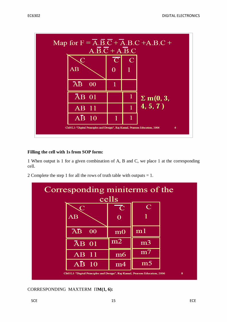
Filling the cell with 1s from SOP form:
1 When output is 1 for a given combination of A, B and C, we place 1 at the corresponding
cell.
2 Complete the step 1 for all the rows of truth table with outputs = 1.
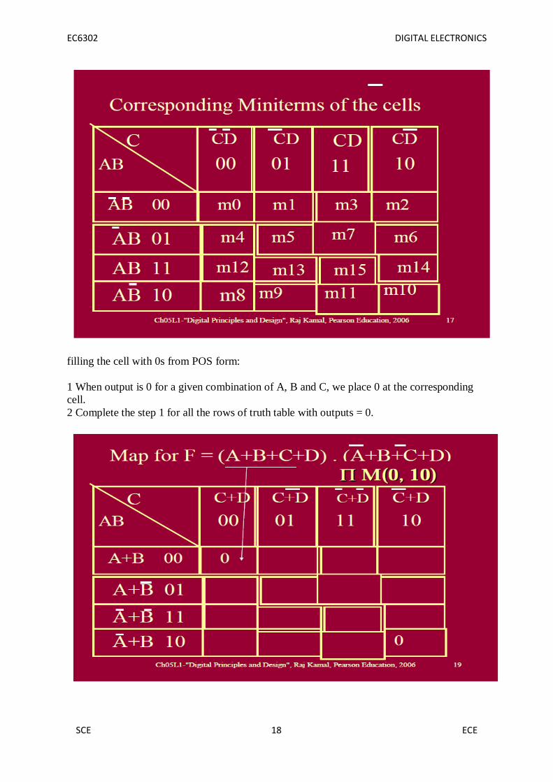
Filling the cell with 0s from POS form:
1 When output is 0 for a given combination of A, B and C, we place 0 at the corresponding
cell.

EC6302 DIGITAL ELECTRONICS
SCE 13 ECE
2 Complete the step 1 for all 8 rows of truth table with outputs = 0.
Map from 3 variables Truth table or SOP form Boolean Expression:
_ A two-dimensional map built from a truth table or 3 variables SOP form Boolean
Expression _ Since number of rows in three variable (three inputs) truth table are 8, the map
has 8 cells _ Two cells horizontal and four cells vertical. [It can also be vice versa.
Σ m(1,3,5,6,7,9,11,13,15) corresponding miniterm of the cells
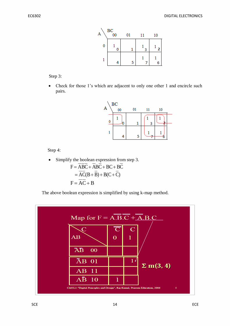
1.10.1THREE VARIABLE KARNAUGHMAP:
Step 1:
Simplify the following Boolean functions, using three variable maps F(A,B,C) =
∑(0,2,3,6,7)?
Draw the K-map diagram for three variable method.
A three variable method contains 23 = 8 cells.
Assign the three variable as A,B,C. for this method in K-map table value
should be in 0 to 7 because its an three variable method.
Step 2:
From the given example enter the value ‘1’ for given decimal value in K-map
diagram.
EC6302 DIGITAL ELECTRONICS
SCE 14 ECE
Step 3:
Check for those 1’s which are adjacent to only one other 1 and encircle such
pairs.
Step 4:
Simplify the boolean expression from step 3.
CBBCCBACBAF
)CC(B)BB(CA
BCAF
The above boolean expression is simplified by using k-map method.
EC6302 DIGITAL ELECTRONICS
SCE 15 ECE
Filling the cell with 1s from SOP form:
1 When output is 1 for a given combination of A, B and C, we place 1 at the corresponding
cell.
2 Complete the step 1 for all the rows of truth table with outputs = 1.
CORRESPONDING MAXTERM ΠM(1, 6):

EC6302 DIGITAL ELECTRONICS
SCE 16 ECE
filling the cell with 0s from POS form:
1 When output is 0 for a given combination of A, B and C, we place 0 at the corresponding
cell.
2 Complete the step 1 for all 8 rows of truth table with outputs = 0.

EC6302 DIGITAL ELECTRONICS
SCE 17 ECE
1.10.2 MAP FROM 4 VARIABLES TRUTH TABLE OR SOP FORM BOOLEAN
EXPRESSION:
_ A two-dimensional map built from a truth table or 4 variables SOP form Boolean
Expression _ Since number of rows in a four variable (three inputs) truth table are 16, the
map has 16 cells _ Four cells horizontal and four cells vertical.
filling the cell with 1s:
1. When output is 1 for a given combination of A, B, C and D, we place 1 at the
corresponding cell.
2. Complete the step 1 for all 16 rows of truth table with outputs = 1.
EC6302 DIGITAL ELECTRONICS
SCE 18 ECE
filling the cell with 0s from POS form:
1 When output is 0 for a given combination of A, B and C, we place 0 at the corresponding
cell.
2 Complete the step 1 for all the rows of truth table with outputs = 0.

EC6302 DIGITAL ELECTRONICS
SCE 19 ECE
1.10.3 FIVE VARIABLE KARNAUGH MAP:
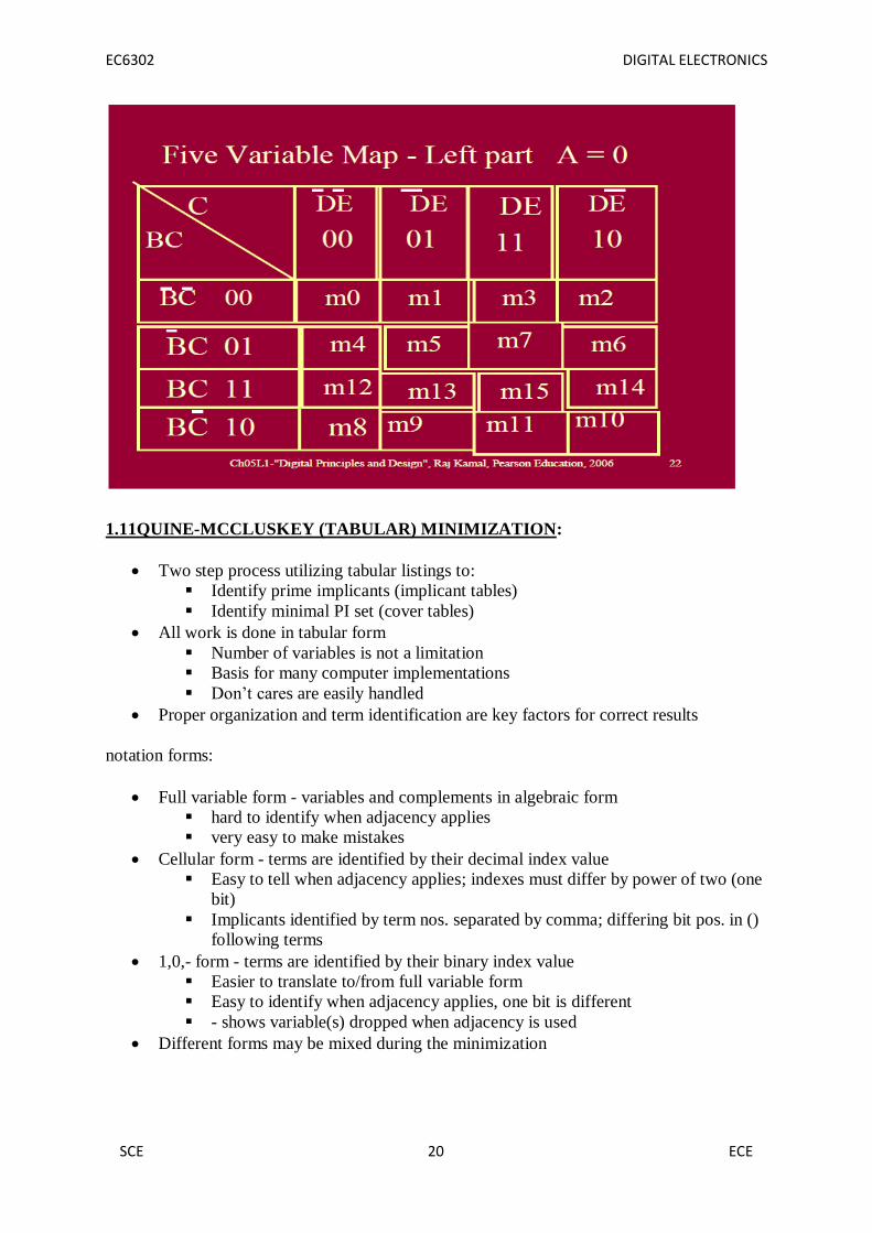
EC6302 DIGITAL ELECTRONICS
SCE 20 ECE
1.11QUINE-MCCLUSKEY (TABULAR) MINIMIZATION:
Two step process utilizing tabular listings to:
Identify prime implicants (implicant tables)
Identify minimal PI set (cover tables)
All work is done in tabular form
Number of variables is not a limitation
Basis for many computer implementations
Don’t cares are easily handled
Proper organization and term identification are key factors for correct results
notation forms:
Full variable form - variables and complements in algebraic form
hard to identify when adjacency applies
very easy to make mistakes
Cellular form - terms are identified by their decimal index value
Easy to tell when adjacency applies; indexes must differ by power of two (one
bit)
Implicants identified by term nos. separated by comma; differing bit pos. in ()
following terms
1,0,- form - terms are identified by their binary index value
Easier to translate to/from full variable form
Easy to identify when adjacency applies, one bit is different
- shows variable(s) dropped when adjacency is used
Different forms may be mixed during the minimization

EC6302 DIGITAL ELECTRONICS
SCE 21 ECE

EC6302 DIGITAL ELECTRONICS
SCE 22 ECE

EC6302 DIGITAL ELECTRONICS
SCE 23 ECE

EC6302 DIGITAL ELECTRONICS
SCE 24 ECE

EC6302 DIGITAL ELECTRONICS
SCE 25 ECE

EC6302 DIGITAL ELECTRONICS
SCE 26 ECE

EC6302 DIGITAL ELECTRONICS
SCE 27 ECE
1.12 LOGIC GATES:
In Boolean algebra, there are three basic logic operations: AND, OR, and NOT.
These logic gates are digital circuits constructed from diodes, transistors, and resistors
connected in such a way that the circuit output is the result of a basic logic operation (OR,
AND, NOT) performed on the inputs.
OR OPERATION
The expression X = A + B reads as "X equals A OR B". The + sign stands for the OR
operation, not for ordinary addition.
The OR operation produces a result of 1 when any of the input variable is 1.
The OR operation produces a result of 0 only when all the input variables are 0.
An example of three input OR gate and its truth table is as follows:

EC6302 DIGITAL ELECTRONICS
SCE 28 ECE
With the OR operation, 1 + 1 = 1, 1+ 1 + 1 = 1 and so on.
AND Operation
The expression X = A * B reads as "X equals A AND B".
The multiplication sign stands for the AND operation, same for ordinary multiplication of 1s
and 0s.The AND operation produces a result of 1 occurs only for the single case when all of
the input variables are 1.The output is 0 for any case where one or more inputs are 0.
An example of three input AND gate and its truth table is as follows:
With the AND operation, 1*1 = 1, 1*1*1 = 1 and so on.
NOT Operation
The NOT operation is unlike the OR and AND operations in that it can be performed on a
single input variable. For example, if the variable A is subjected to the NOT operation, the
result x can be expressed as x = A' where the prime (') represents the NOT operation. This

EC6302 DIGITAL ELECTRONICS
SCE 29 ECE
expression is read as:
x equals NOT A
x equals the inverse of A
x equals the complement of A
Each of these is in common usage and all indicate that the logic value of x = A' is opposite to
the logic value of A. The truth table of the NOT operation is as follows:
1'=0 because NOT 1 is 0
0' = 1 because NOT 0 is 1
The NOT operation is also referred to as inversion or complementation, and these terms are
used interchangeably.
NOR Operation
NOR and NAND gates are used extensively in digital circuitry. These gates combine the
basic operations AND, OR and NOT, which make it relatively easy to describe then using
Boolean algebra.NOR gate symbol is the same as the OR gate symbol except that it has a
small circle on the output. This small circle represents the inversion operation. Therefore the
output expression of the two input NOR gate is:
X = (A + B)'

EC6302 DIGITAL ELECTRONICS
SCE 30 ECE
An example of three inputs OR gate can be constructed by a NOR gate plus a NOT gate:
NAND Operation
NAND gate symbol is the same as the AND gate symbol except that it has a small circle on
the output. This small circle represents the inversion operation. Therefore the output
expression of the two input NAND gate is:
X = (AB)'
Ex-NOR Gate Equivalent
EC6302 DIGITAL ELECTRONICS
SCE 31 ECE
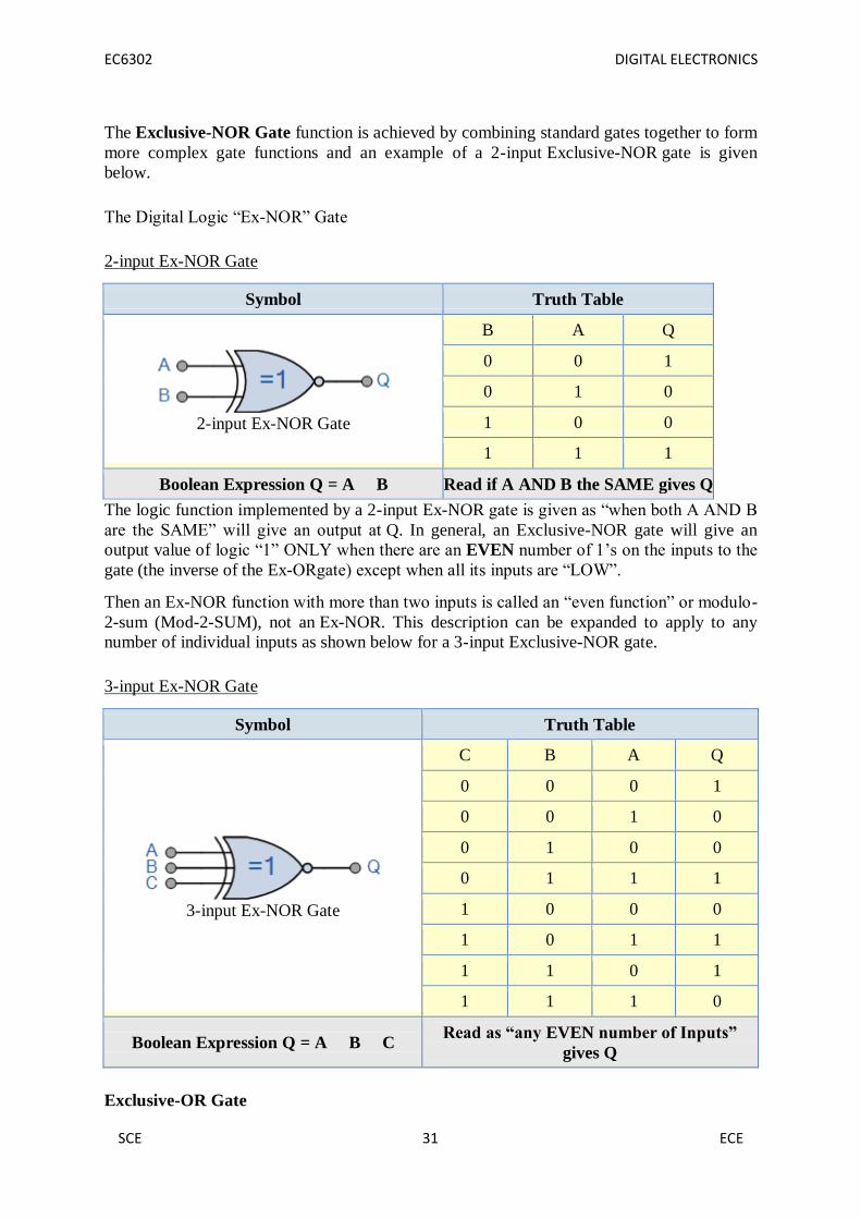
The Exclusive-NOR Gate function is achieved by combining standard gates together to form
more complex gate functions and an example of a 2-input Exclusive-NOR gate is given
below.
The Digital Logic “Ex-NOR” Gate
2-input Ex-NOR Gate
Symbol Truth Table
2-input Ex-NOR Gate
B A Q
0 0 1
0 1 0
1 0 0
1 1 1
Boolean Expression Q = A B Read if A AND B the SAME gives Q
The logic function implemented by a 2-input Ex-NOR gate is given as “when both A AND B
are the SAME” will give an output at Q. In general, an Exclusive-NOR gate will give an
output value of logic “1” ONLY when there are an EVEN number of 1’s on the inputs to the
gate (the inverse of the Ex-ORgate) except when all its inputs are “LOW”.
Then an Ex-NOR function with more than two inputs is called an “even function” or modulo-
2-sum (Mod-2-SUM), not an Ex-NOR. This description can be expanded to apply to any
number of individual inputs as shown below for a 3-input Exclusive-NOR gate.
3-input Ex-NOR Gate
Symbol Truth Table
3-input Ex-NOR Gate
C B A Q
0 0 0 1
0 0 1 0
0 1 0 0
0 1 1 1
1 0 0 0
1 0 1 1
1 1 0 1
1 1 1 0
Boolean Expression Q = A B C Read as “any EVEN number of Inputs”
gives Q
Exclusive-OR Gate

EC6302 DIGITAL ELECTRONICS
SCE 32 ECE
2-input Ex-OR Gate
Symbol Truth Table
2-input Ex-OR Gate
B A Q
0 0 0
0 1 1
1 0 1
1 1 0
Boolean Expression Q = A B A OR B but NOT BOTH gives Q
The truth table above shows that the output of an Exclusive-OR gate ONLY goes “HIGH”
when both of its two input terminals are at “DIFFERENT” logic levels with respect to each
other. If these two inputs, A and B are both at logic level “1” or both at logic level “0” the
output is a “0” making the gate an “odd but not the even gate”.
This ability of the Exclusive-OR gate to compare two logic levels and produce an output
value dependent upon the input condition is very useful in computational logic circuits as it
gives us the following Boolean expression of:
Q = (A B) = A.B + A.B
The logic function implemented by a 2-input Ex-OR is given as either: “A OR B but NOT
both” will give an output at Q. In general, an Ex-OR gate will give an output value of logic
“1” ONLY when there are an ODD number of 1’s on the inputs to the gate, if the two
numbers are equal, the output is “0”.
Then an Ex-OR function with more than two inputs is called an “odd function” or modulo-2-
sum (Mod-2-SUM), not an Ex-OR. This description can be expanded to apply to any number
of individual inputs as shown below for a 3-input Ex-OR gate.
3-input Ex-OR Gate
Symbol Truth Table
3-input Ex-OR Gate
C B A Q
0 0 0 0
0 0 1 1
0 1 0 1
0 1 1 0
1 0 0 1
1 0 1 0
1 1 0 0
1 1 1 1
Boolean Expression Q = A B C “Any ODD Number of Inputs” gives Q

EC6302 DIGITAL ELECTRONICS
SCE 33 ECE
1.13 NAND–NOR IMPLEMENTATIONS
Universal gates are the ones which can be used for implementing any gate like AND, OR and
NOT, or any combination of these basic gates; NAND and NOR gates are universal gates.
But there are some rules that need to be followed when implementing NAND or NOR based
gates.
To facilitate the conversion to NAND and NOR logic, we have two new graphic symbols for
these gates.
NAND Gate

EC6302 DIGITAL ELECTRONICS
SCE 34 ECE
NOR Gate
Realization of logic function using NAND gates Any logic function can be implemented using NAND gates. To achieve this, first the logic
function has to be written in Sum of Product (SOP) form. Once logic function is converted
to SOP, then is very easy to implement using NAND gate. In other words any logic circuit
with AND gates in first level and OR gates in second level can be converted into a NAND-
NAND gate circuit.
Consider the following SOP expression
F = W.X.Y + X.Y.Z + Y.Z.W
The above expression can be implemented with three AND gates in first stage and one OR
gate in second stage as shown in figure.
If bubbles are introduced at AND gates output and OR gates inputs (the same for NOR
gates), the above circuit becomes as shown in figure.
Now replace OR gate with input bubble with the NAND gate. Now we have circuit which is
fully implemented with just NAND gates.

EC6302 DIGITAL ELECTRONICS
SCE 35 ECE
Realization of logic gates using NAND gates
Implementing an inverter using NAND gate
Input Output Rule
(X.X)' = X' Idempotent
Implementing AND using NAND gates
Input Output Rule
((XY)'(XY)')' = ((XY)')' Idempotent
= (XY) Involution
Implementing OR using NAND gates
Input Output Rule
((XX)'(YY)')' = (X'Y')' Idempotent
= X''+Y'' DeMorgan
= X+Y Involution

EC6302 DIGITAL ELECTRONICS
SCE 36 ECE
Implementing NOR using NAND gates
Input Output Rule
((XX)'(YY)')' =(X'Y')' Idempotent
=X''+Y'' DeMorgan
=X+Y Involution
=(X+Y)' Idempotent
Realization of logic function using NOR gates Any logic function can be implemented using NOR gates. To achieve this, first the logic
function has to be written in Product of Sum (POS) form. Once it is converted to POS, then
it's very easy to implement using NOR gate. In other words any logic circuit with OR gates
in first level and AND gates in second level can be converted into a NOR-NOR gate circuit.
Consider the following POS expression
F = (X+Y) . (Y+Z)
The above expression can be implemented with three OR gates in first stage and one AND
gate in second stage as shown in figure.
If bubble are introduced at the output of the OR gates and the inputs of AND gate, the above
circuit becomes as shown in figure.

EC6302 DIGITAL ELECTRONICS
SCE 37 ECE
Now replace AND gate with input bubble with the NOR gate. Now we have circuit which is
fully implemented with just NOR gates.
Realization of logic gates using NOR gates
Implementing an inverter using NOR gate
Input Output Rule
(X+X)' = X' Idempotent
Implementing AND using NOR gates
Input Output Rule
((X+X)'+(Y+Y)')' =(X'+Y')' Idempotent
= X''.Y'' DeMorgan
= (X.Y) Involution

EC6302 DIGITAL ELECTRONICS
SCE 38 ECE
Implementing OR using NOR gates
Input Output Rule
((X+Y)'+(X+Y)')' = ((X+Y)')' Idempotent
= X+Y Involution
Implementing NAND using NOR gates
Input Output Rule
((X+Y)'+(X+Y)')' = ((X+Y)')' Idempotent
= X+Y Involution
= (X+Y)' Idempotent
1.14 TTL FAMILY OF ICS:
The TTL NAND gate is broken up into three basic sections: multiemitter input, control
section, and totem-pole output stage. In the multiemitter input section, a multiemitter bipolar
transistor Q1 acts like a two-input ANDgate, while diodesD1 andD2 act as negative clamping
diodes used to protect the inputs from any short-term negative input voltages that could
damage the ransistor. Q2 provides control and current boosting to the totem-pole output
stage; when the output is high (1), Q4 is off (open) and Q3 is on (short).When the output is
low (0), Q4 is on and Q3 is off. Because one or the other transistor is always off, the current

EC6302 DIGITAL ELECTRONICS
SCE 39 ECE
flow from VCC to ground in that section of the circuit is minimized. The lower figures show
both a high and low output state, along with the approximate voltages present at various
locations.
Notice that the actual output voltages are not exactly 0 or +5V—a result of internal voltage
drops across resistor, transistor, and diode. Instead, the outputs are around 3.4V for high and
0.3V for low. As a note, to create, say, an eight-input NAND gate, the multiemitter input
transistor would have eight emitters instead of just two as shown.
Asimple modification to the standard TTL series was made early on by reducing all the
internal resistor values in order to reduce the RC time constants and thus increase the speed
(reduce propagation delays). This improvement to the original TTL series marked the 74H
series. Although the 74H series offered improved speed (about twice as fast) over the 74
series, it had more than double the power consumption. Later, the 74L series emerged. Unlike
the 74H, the 74L took the 74 and increased all internal resistances. The net effect lead to a
reduction in power but increased propagation delay. A significant improvement in speed
within the TTL line emerged with the development of the 74Sxx series (Schottky TTL series).
The key modifications involved placing Schottky diodes across the base-to-collector
junctions of the transistors. These Schottky diodes eliminated capacitive effects caused by
charge buildup in the transistor’s base region by passing the charge to the collector region.
Schottky diodes were the best choice because of their inherent low charge buildup
characteristics. The overall effect was an increase in speed by a factor of 5 and only a
doubling in power. Continually over time, by using different integration techniques and
increasing the values of the internal resistors, more power-efficient series emerged, like the
lowpower Schottky 74LS series, with about one-third the power dissipation of the 74S. After
EC6302 DIGITAL ELECTRONICS
SCE 40 ECE
the 74LS, the advanced-low-power Schottky 74ALS series emerged, which had even better
performance. Another series developed around this time was the 74F series, or FAST logic,
which used a new process of integration called oxide isolation (also used in the ALS series)
that led to reduced propagation delays and decreased the overall size.
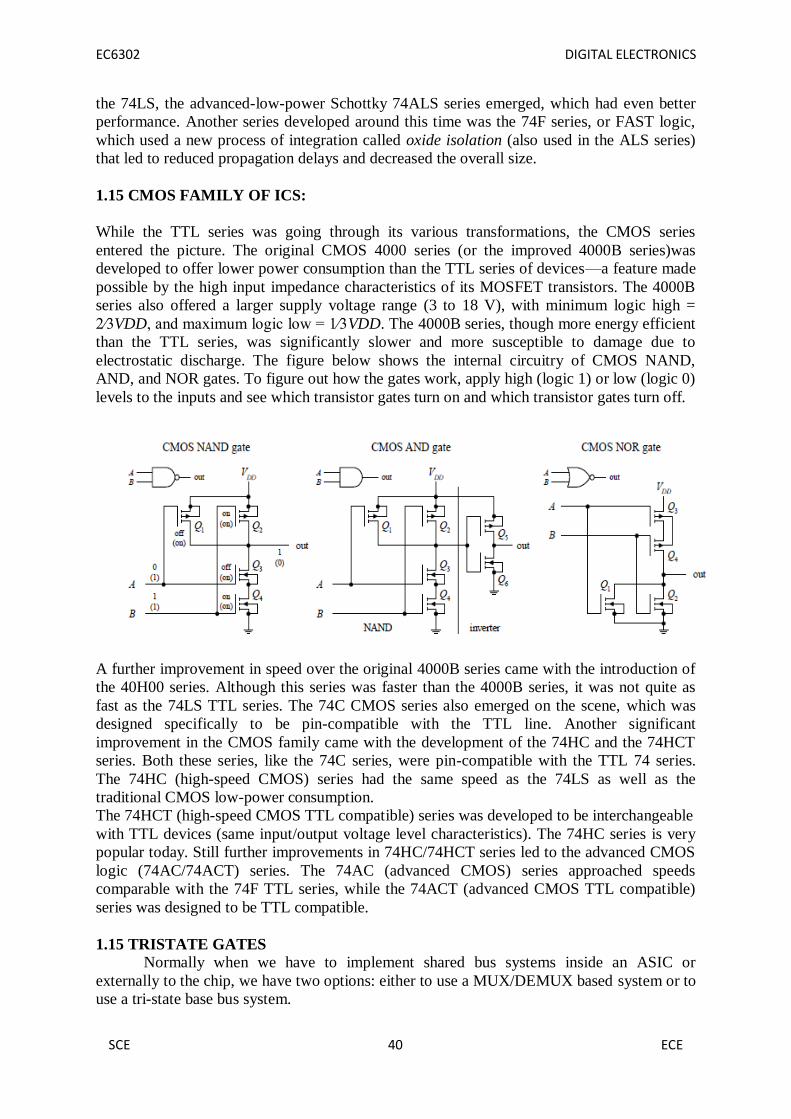
1.15 CMOS FAMILY OF ICS:
While the TTL series was going through its various transformations, the CMOS series
entered the picture. The original CMOS 4000 series (or the improved 4000B series)was
developed to offer lower power consumption than the TTL series of devices—a feature made
possible by the high input impedance characteristics of its MOSFET transistors. The 4000B
series also offered a larger supply voltage range (3 to 18 V), with minimum logic high =
2⁄3VDD, and maximum logic low = 1⁄3VDD. The 4000B series, though more energy efficient
than the TTL series, was significantly slower and more susceptible to damage due to
electrostatic discharge. The figure below shows the internal circuitry of CMOS NAND,
AND, and NOR gates. To figure out how the gates work, apply high (logic 1) or low (logic 0)
levels to the inputs and see which transistor gates turn on and which transistor gates turn off.
A further improvement in speed over the original 4000B series came with the introduction of
the 40H00 series. Although this series was faster than the 4000B series, it was not quite as
fast as the 74LS TTL series. The 74C CMOS series also emerged on the scene, which was
designed specifically to be pin-compatible with the TTL line. Another significant
improvement in the CMOS family came with the development of the 74HC and the 74HCT
series. Both these series, like the 74C series, were pin-compatible with the TTL 74 series.
The 74HC (high-speed CMOS) series had the same speed as the 74LS as well as the
traditional CMOS low-power consumption.
The 74HCT (high-speed CMOS TTL compatible) series was developed to be interchangeable
with TTL devices (same input/output voltage level characteristics). The 74HC series is very
popular today. Still further improvements in 74HC/74HCT series led to the advanced CMOS
logic (74AC/74ACT) series. The 74AC (advanced CMOS) series approached speeds
comparable with the 74F TTL series, while the 74ACT (advanced CMOS TTL compatible)
series was designed to be TTL compatible.
1.15 TRISTATE GATES Normally when we have to implement shared bus systems inside an ASIC or
externally to the chip, we have two options: either to use a MUX/DEMUX based system or to
use a tri-state base bus system.

EC6302 DIGITAL ELECTRONICS
SCE 41 ECE
In the latter, when logic is not driving its output, it does not drive LOW neither
HIGH, which means that logic output is floating. Well, one may ask, why not just use an
open collector for shared bus systems? The problem is that open collectors are not so good
for implementing wire-ANDs.
The circuit below is a tri-state NAND gate; when Enable En is HIGH, it works like
any other NAND gate. But when Enable En is driven LOW, Q1 Conducts, and the diode
connecting Q1 emitter and Q2 collector, conducts driving Q3 into cut-off. Since Q2 is not
conducting, Q4 is also at cut-off. When both pull-up and pull-down transistors are not
conducting, output Z is in high-impedance state.

EC6302 DIGITAL ELECTRONICS
SCE 42 ECE
UNIT 2-COMBINATIONAL CIRCUITS
2.1 HALF ADDER:
• Design a logic circuit to add two bits and produce a sum bit and a carry bit. Two
inputs and two outputs are needed. Let us call the inputs x and y, and the outputs S
and C.
• A half adder
– For adding 2 bits
– Gives “carry out” and “sum”
– 1 AND and 1 XOR gate
2.2 FULL-ADDER:
Adding two single-bit binary values, X, Y with a carry input bit C-in produces a sum bit S
and a carry out C-out bit.

EC6302 DIGITAL ELECTRONICS
SCE 43 ECE
• A full adder
– For adding 2 bits plus a “carry in”
– Gives “carry out” and “sum”
– 2 ANDs, 2 XORs, and 1 OR

EC6302 DIGITAL ELECTRONICS
SCE 44 ECE
2.2.1 FULL ADDER CIRCUIT USING AND-OR:
2.2.2 FULL ADDER CIRCUIT USING XOR:
2.3 SUBTRACTOR
Subtractor circuits take two binary numbers as input and subtract one binary number
input from the other binary number input. Similar to adders, it gives out two outputs,
difference and borrow (carry-in the case of Adder). There are two types of subtractors.
Half Subtractor

EC6302 DIGITAL ELECTRONICS
SCE 45 ECE
Full Subtractor
2.3.1 Half Subtractor
The half-subtractor is a combinational circuit which is used to perform subtraction of
two bits. It has two inputs, X (minuend) and Y (subtrahend) and two outputs D (difference)
and B (borrow). The logic symbol and truth table are shown below.
Symbol
Truth Table
X Y D B
0 0 0 0
0 1 1 1
1 0 1 0
1 1 0 0
From the above table we can draw the Kmap as shown below for "difference" and
"borrow". The boolean expression for the difference and Borrow can be written.
From the equation we can draw the half-subtractor as shown in the figure below.
EC6302 DIGITAL ELECTRONICS
SCE 46 ECE
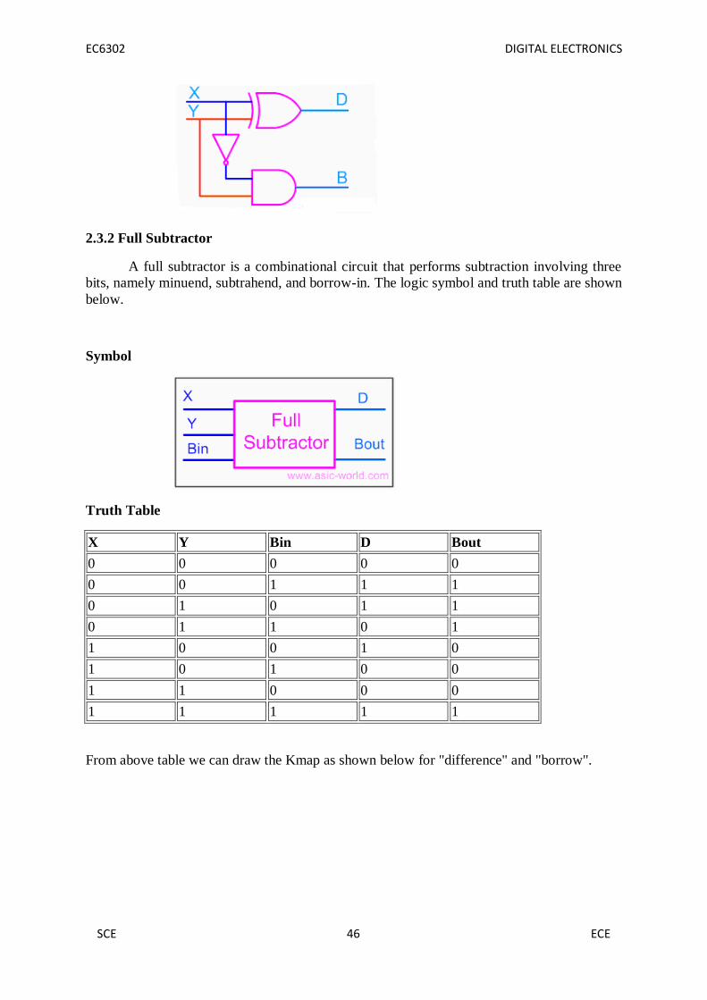
2.3.2 Full Subtractor
A full subtractor is a combinational circuit that performs subtraction involving three
bits, namely minuend, subtrahend, and borrow-in. The logic symbol and truth table are shown
below.
Symbol
Truth Table
X Y Bin D Bout
0 0 0 0 0
0 0 1 1 1
0 1 0 1 1
0 1 1 0 1
1 0 0 1 0
1 0 1 0 0
1 1 0 0 0
1 1 1 1 1
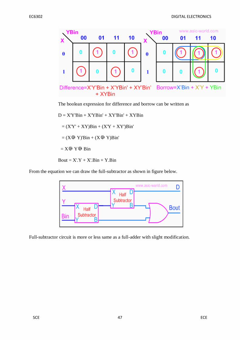
From above table we can draw the Kmap as shown below for "difference" and "borrow".
EC6302 DIGITAL ELECTRONICS
SCE 47 ECE
The boolean expression for difference and borrow can be written as
D = X'Y'Bin + X'YBin' + XY'Bin' + XYBin
= (X'Y' + XY)Bin + (X'Y + XY')Bin'
= (X Y)'Bin + (X Y)Bin'
= X Y Bin
Bout = X'.Y + X'.Bin + Y.Bin
From the equation we can draw the full-subtractor as shown in figure below.
Full-subtractor circuit is more or less same as a full-adder with slight modification.

EC6302 DIGITAL ELECTRONICS
SCE 48 ECE
2.4-BIT BINARY PARALLEL ADDER AND SUBTRACTOR:
To add two 4-bit binary number, we proceed as shown in the table. The table shows the role
of carry-in and carry-out.
4-bit binary parallel adder can be implemented in integrated circuit form by cascading 4 full
adders as shown below. The disadvantage of this adder is the possible slowing down of the
addition due to the carry propagation time.

EC6302 DIGITAL ELECTRONICS
SCE 49 ECE
The 4-bit parallel adder can be modified to work as 4-bit parallel adder/subtractor b including
4 exclusive-OR gates to provide the 1's complement of B and adding 1 from the M input to
make it the 2's complement.
2.5 CARRY PROPAGATION AND THE LOOK-AHEAD CARRY CIRCUIT:
The carry propagate (Pi) and carry generate (Gi) variables are shown on the full adder logic
circuit. The carries C1, C2, and C3 can be expressed in SOP form as functions of C0 and the
different (Pi) and (Gi) as follows:
The logic diagram of the look-ahead generator is implemented in a two level form as shown
in the following logic circuit.

EC6302 DIGITAL ELECTRONICS
SCE 50 ECE

EC6302 DIGITAL ELECTRONICS
SCE 51 ECE
The 4-bit adder with the carry look-ahead circuit is implemented as shown in the following
circuit.
2.6 SERIAL ADDER WITH ACCUMULATOR:
• The full adder is used to perform bit by bit addition and D-Flip flop is used to store
the
• carry output generated after addition.
• This carry is used to carry input for the next addition. Initially the D Flip flop is
cleared and addition starts with the least significant bits of both register.

EC6302 DIGITAL ELECTRONICS
SCE 52 ECE
• After each clock pulse data within the right shift registers are shifted right 1-bit and
We get from next digit and carry of precious addition as new inputs for the full adder.
2.7 SERIAL SUBTRACTOR:
In this circuit, we have Input number coming bit by bit and output comes bit by bit and the
final borrow at the end:
Serial Subtractor

EC6302 DIGITAL ELECTRONICS
SCE 53 ECE
2.8 BCD ADDER:
When the sum of two digits is less than or equal to 9 then the ordinary 4-bit adder can
be used
But if the sum of two digits is greater than 9 then a correction must be added “I.e
adding 0110”
We need to design a circuit that is capable of doing the correct addition
The cases where the sum of two 4-bit numbers is greater than 9 are in the following
table:
S4 S3 S2 S1 S0
0 1 0 1 0 10
0 1 0 1 1 11
0 1 1 0 0 12
0 1 1 0 1 13
0 1 1 1 0 14
0 1 1 1 1 15
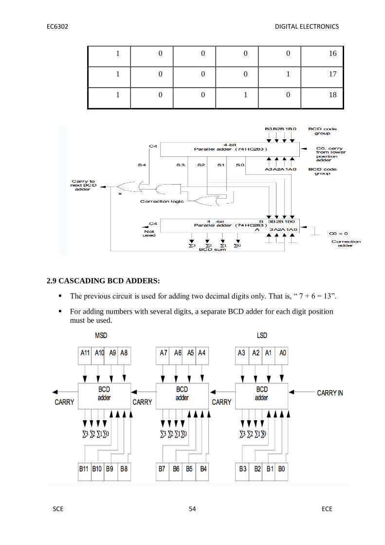
EC6302 DIGITAL ELECTRONICS
SCE 54 ECE
1 0 0 0 0 16
1 0 0 0 1 17
1 0 0 1 0 18
2.9 CASCADING BCD ADDERS:
The previous circuit is used for adding two decimal digits only. That is, “ 7 + 6 = 13”.
For adding numbers with several digits, a separate BCD adder for each digit position
must be used.

EC6302 DIGITAL ELECTRONICS
SCE 55 ECE
Example:
Determine the inputs and the outputs when the above circuit is used to add 538 to 247.
Assume a CARRY IN = 0
Solution:
Represent the decimal numbers in BCD
247 = 0010 0100 0111
538 = 0101 0011 1000
Put these numbers in registers [A] and [B]
[A] = 0010 0100 0111
[B] = 0101 0011 1000
Example:
?
2.10 BINARY MULTIPLIER:
Multiplication of binary numbers is performed in the same way as in decimal numbers –
partial product: the multiplicand is multiplied by each bit of the multiplier starting from the
least significant bit

EC6302 DIGITAL ELECTRONICS
SCE 56 ECE
Multiplication of two bits = A * B (AND)
0 * 0 = 0 0 * 1 = 0 1 * 0 = 0 1 * 1 = 1
2.10.1 2-BIT BY 2-BIT BINARY MULTIPLIER:
2.10.2 4-BIT BY 3-BIT BINARY MULTIPLIER:

EC6302 DIGITAL ELECTRONICS
SCE 57 ECE
2.11 MULTIPLEXER:
A multiplexer (MUX) is a digital switch which connects data from one of n sources to
the output. A number of select inputs determine which data source is connected to the output.
The block diagram of MUX with n data sources of b bits wide and s bits wide select line is
shown in below figure.
MUX acts like a digitally controlled multi-position switch where the binary code
applied to the select inputs controls the input source that will be switched on to the output as
shown in the figure below. At any given point of time only one input gets selected and is
connected to output, based on the select input signal.
The operation of a multiplexer can be better explained using a mechanical switch as
shown in the figure below. This rotary switch can touch any of the inputs, which is connected
to the output. As you can see at any given point of time only one input gets transferred to
output.
2x1 MUX
A 2 to 1 line multiplexer is shown in figure below, each 2 input lines A to B is applied
to one input of an AND gate. Selection lines S are decoded to select a particular AND gate.
The truth table for the 2:1 mux is given in the table below.
Design of a 2:1 Mux
To derive the gate level implementation of 2:1 mux we need to have truth table as
shown in figure. And once we have the truth table, we can draw the K-map as shown in
figure for all the cases when Y is equal to '1'.Combining the two 1' as shown in figure, we can
drive the output y as shown below
Y = A.S’ + B.S
Truth Table
B A S Y

EC6302 DIGITAL ELECTRONICS
SCE 58 ECE
0 0 0 0
0 0 1 0
0 1 0 1
0 1 1 0
1 0 0 0
1 0 1 1
1 0 1
1 1 1 1
Kmap
Circuit
LARGER MULTIPLEXERS
Larger multiplexers can be constructed from smaller ones. An 8-to-1 multiplexer can
be constructed from smaller multiplexers as shown below.
8-to-1 multiplexer from Smaller MUX

EC6302 DIGITAL ELECTRONICS
SCE 59 ECE
16-to-1 multiplexer from 4:1 mux
Quadruple 2-to-1 MUX
It is 2-to-1 MUX with 4 bits for each input
There is 1 output of 4 bits
There is 1 select signal
When 1 input is selected, the whole group of 4 bits goes to the output
3-variable Function Using 8-to-1 mux
Implement the function F(X,Y,Z) = S(1,3,5,6) using an 8-to-1 mux. Connect the input
variables X, Y, Z to mux select lines. Mux data input lines 1, 3, 5, 6 that correspond to the
function minterms are connected to 1. The remaining mux data input lines 0, 2, 4, 7 are
connected to 0.

EC6302 DIGITAL ELECTRONICS
SCE 60 ECE
3-variable Function Using 4-to-1 mux
Implement the function F(X,Y,Z) = S(0,1,3,6) using a single 4-to-1 mux and an
inverter. We choose the two most significant inputs X, Y as mux select lines.
Truth Table
Select i X Y Z F Mux Input
i
0 0 0 0 1 1
0 0 0 1 1 1
1 0 1 0 0 Z
1 0 1 1 1 Z
2 1 0 0 0 0
2 1 0 1 0 0
3 1 1 0 1 Z'
3 1 1 1 0 Z'
We determine multiplexer input line i values by comparing the remaining input variable Z
and the function F for the corresponding selection lines value i
when XY=00 the function F is 1 (for both Z=0, Z=1) thus mux input0 = 1
when XY=01 the function F is Z thus mux input1 = Z
when XY=10 the function F is 0 (for both Z=0, Z=1) thus mux input2 = 0
when XY=11 the function F is Z' thus mux input3 = Z'

EC6302 DIGITAL ELECTRONICS
SCE 61 ECE
2.12 DE-MULTIPLEXERS
They are digital switches which connect data from one input source to one of n
outputs.Usually implemented by using n-to-2n binary decoders where the decoder enable line
is used for data input of the de-multiplexer.The figure below shows a de-multiplexer block
diagram which has got s-bits-wide select input, one b-bits-wide data input and n b-bits-wide
outputs.
The operation of a de-multiplexer can be better explained using a mechanical switch
as shown in the figure below. This rotary switch can touch any of the outputs, which is
connected to the input. As you can see at any given point of time only one output gets
connected to input.

EC6302 DIGITAL ELECTRONICS
SCE 62 ECE
1-to-4 De-multiplexer
Truth Table
S1 S0 F0 F1 F2 F3
0 0 D 0 0 0
0 1 0 D 0 0
1 0 0 0 D 0
1 1 0 0 0 D
2.13 ENCODERS
An encoder is a combinational circuit that performs the inverse operation of a
decoder. If a device output code has fewer bits than the input code has, the device is usually
called an encoder. e.g. 2n-to-n, priority encoders.
The simplest encoder is a 2n-to-n binary encoder, where it has only one of 2
n inputs =
1 and the output is the n-bit binary number corresponding to the active input. It can be built
from OR gates
e.g. 4-to-2 Encoder
Octal-to-Binary Encoder
Octal-to-Binary take 8 inputs and provides 3 outputs, thus doing the opposite of what
the 3-to-8 decoder does. At any one time, only one input line has a value of 1. The figure
below shows the truth table of an Octal-to-binary encoder.
Truth Table
I0 I1 I2 I3 I4 I5 I6 I7 Y2 Y1 Y0
1 0 0 0 0 0 0 0 0 0 0

EC6302 DIGITAL ELECTRONICS
SCE 63 ECE
0 1 0 0 0 0 0 0 0 0 1
0 0 1 0 0 0 0 0 0 1 0
0 0 0 1 0 0 0 0 0 1 1
0 0 0 0 1 0 0 0 1 0 0
0 0 0 0 0 1 0 0 1 0 1
0 0 0 0 0 0 1 0 1 1 0
0 0 0 0 0 0 0 1 1 1 1
For an 8-to-3 binary encoder with inputs I0-I7 the logic expressions of the outputs Y0-Y2
are:
Y0 = I1 + I3 + I5 + I7
Y1= I2 + I3 + I6 + I7
Y2 = I4 + I5 + I6 +I7
Based on the above equations, we can draw the circuit as shown below
2.14 DECODERS:
A combinational circuit that converts binary information from n input lines to a maximum of
2n unique output lines
n-to-m-line decoders: generate m (=2n or fewer) minterms of n input variables A n-to-2n
decoder takes an n-bit input and produces 2n outputs. The n inputs represent a binary number
that determines which of the 2n outputs is uniquely true.
• A 2-to-4 decoder operates according to the following truth table. – The 2-bit input is called
S1S0, and the four outputs are Q0-Q3. – If the input is the binary number i, then output Qi is
uniquely true.
• For instance, if the input S1 S0 = 10 (decimal 2), then output Q2 is
true, and Q0, Q1, Q3 are all false.
• This circuit “decodes” a binary number into a “one-of-four” code.
Follow the design procedures from last time! We have a truth table, so we can write
equations for each of the four outputs (Q0-Q3), based on the two inputs (S0-S1).
EC6302 DIGITAL ELECTRONICS
SCE 64 ECE
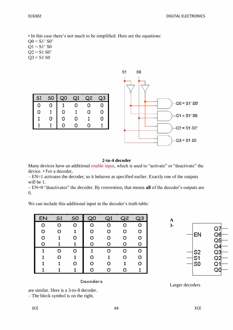
• In this case there’s not much to be simplified. Here are the equations:
Q0 = S1’ S0’
Q1 = S1’ S0
Q2 = S1 S0’
Q3 = S1 S0
2-to-4 decoder
Many devices have an additional enable input, which is used to “activate” or “deactivate” the
device. • For a decoder,
– EN=1 activates the decoder, so it behaves as specified earlier. Exactly one of the outputs
will be 1.
– EN=0 “deactivates” the decoder. By convention, that means all of the decoder’s outputs are
0.
We can include this additional input in the decoder’s truth table:
A
3-
Larger decoders
are similar. Here is a 3-to-8 decoder.
– The block symbol is on the right.

EC6302 DIGITAL ELECTRONICS
SCE 65 ECE
– A truth table (without EN) is below.
– Output equations are at the bottom right.
• Again, only one output is true for any input combination
3-TO-8 DECODER

EC6302 DIGITAL ELECTRONICS
SCE 66 ECE
2.15 PARITY GENERATOR AND CHECKER:
A parity bit added to n-bit code to produce an n + 1 bit code:
• Add odd parity bit to generate code words with even parity
• Add even parity bit to generate code words with odd parity
• Use odd parity circuit to check code words with even parity
• Use even parity circuit to check code words with odd parity
Example: n = 3. Generate even parity code words of length four
with odd parity generator:
Check even parity code words of length four with odd parity checker:
Operation: (X,Y,Z) = (0,0,1) gives (X,Y,Z,P) = (0,0,1,1) and E = 0.
If Y changes from 0 to 1 between generator and checker, then E = 1 indicates an error
Often, external noise will corrupt binary information (cause a bit to flip from one
logic state to the other) as it travels along a conductor from one device to the next. For
example, in the 4-bit system shown in Fig. 12.51, a BCD 4 (0100) picks up noise and
becomes 0101 (or 5) before reaching its destination. Depending on the application, this type
of error could lead to some serious problems.
To avoid problems caused by unwanted data corruption, a parity generator/ checker
system, like the one shown in Fig can be used.

EC6302 DIGITAL ELECTRONICS
SCE 67 ECE
The basic idea is to add an extra bit, called a parity bit, to the digital information being
transmitted. If the parity bit makes thesumof all transmitted bits (including the parity bit) odd,
the transmitted information is of odd parity.
If the parity bit makes the sum even, the transmitted information is of even parity.Aparity
generator circuit creates the parity bit, while the parity checker on the receiving end
determines if the information sent is of the proper parity.
The type of parity (odd or even) is agreed to beforehand, so the parity checker knows what to
look for. The parity bit can be placed next to the MSB or the LSB, provided the device on the
receiving end knows which bit is the parity bit and which bits are the data. The arrangement
shown in Fig is designed with an even-parity error-detection system.
If you want to avoid building parity generators and checkers from scratch, use a parity
generator/checker IC like the 74F280 9-bit odd-even parity generator/checker shown below.
To make a complete error-detection system, two 74F280s are used—one acts as the parity
generator; the other acts as the parity checker. The generator’s inputs A through H are
connected to the eight data lines of the transmitting portion of the circuit. The ninth input (I)
is grounded when the device is used as a generator. If you want to create an odd-parity
generator, you tap the Σodd output; for even parity, you tap Σeven. The 74F280 checker taps
the main line at the receiving end and also accepts the parity bit line at input I. The figure
below shows an odd-parity error-detection system used with an 8-bit system. If an error
occurs, a high (1) is generated at the Σodd output.

EC6302 DIGITAL ELECTRONICS
SCE 68 ECE
2.16 CODE CONVERTERS
Binary-to-Gray
The table that follows shows natural-binary numbers (upto 4-bit) and corresponding gray
codes.
Looking at gray-code (G3G2G1G0), we find that any two subsequent numbers differ in only
one bit-change.
The same table is used as truth-table for designing a logic circuitry that converts a given 4-bit
natural binary number into gray number. For this circuit, B3 B2 B1 B0 are inputs while
G3 G2 G1 G0 are outputs.
K-map for the outputs:
And G3 = B3
EC6302 DIGITAL ELECTRONICS
SCE 69 ECE
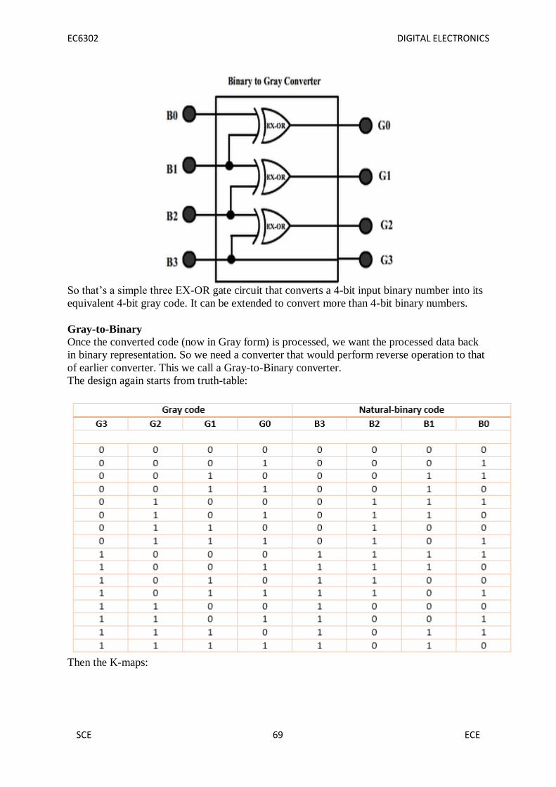
So that’s a simple three EX-OR gate circuit that converts a 4-bit input binary number into its
equivalent 4-bit gray code. It can be extended to convert more than 4-bit binary numbers.
Gray-to-Binary
Once the converted code (now in Gray form) is processed, we want the processed data back
in binary representation. So we need a converter that would perform reverse operation to that
of earlier converter. This we call a Gray-to-Binary converter.
The design again starts from truth-table:
Then the K-maps:

EC6302 DIGITAL ELECTRONICS
SCE 70 ECE
And B3 = G3
The realization of Gray-to-Binary converter is
2.17 COMPARATOR :
Comparator compares binary numbers.
Logic comparing 2 bits: a and b
Magnitude Comparator
Comparator compares binary numbers
4-bit Magnitude Comparator:
Inputs: A3A2A1A0 & B3B2B1B0
Outputs: Y A>B, Y A<B, Y A=B
For each bit, let:
Si = AiBi + Ai’Bi’ = (AiBi’ + Ai’Bi)’

EC6302 DIGITAL ELECTRONICS
SCE 71 ECE
Si is true when Ai = Bi
For A = B, we must have:
A3=B3 and A2=B2 and A1=B1 and A0=B0
Hence, Y A=B = S3•S2•S1•S0 136
Logic For A > B
For A > B, there are 4 cases:
1. A3B3 is 10 and A2A1A0 & B2B1B0 can be anything:
A=1xxx, B=0xxx
2. A3=B3 and A2B2 is 10 and A1A0 & B1B0 can be
anything: A=11xx, B=10xx or A=01xx, B=00xx
3. A3=B3 and A2=B2 and A1B1=10 and A0B0 is xx: e.g.
A=011x, B=010x
4. A3=B3 and A2=B2 and A1=B1 and A0B0 is 10: e.g.
A=1011, B=1010
Y A>B=A3B3’+S3A2B2’+S3S2A1B1’+S3S2S1A0B0’
Logic For A < B
For A < B, there are also 4 cases:
1) A3B3 is 01 and A2A1A0 & B2B1B0 can be anything:
1. A=0xxx, B=1xxx
2) A3=B3 and A2B2 is 01 and A1A0 & B1B0 can be
1. anything: A=10xx, B=11xx or A=00xx, B=01xx
3) A3=B3 and A2=B2 and A1B1=01 and A0B0 is xx: e.g.
1. A=110x, B=111x
4) A3=B3 and A2=B2 and A1=B1 and A0B0 is 01: e.g.
1. A=1000, B=1001
Y A<B=A3 ’B3+S3A2 ’B2+S3S2A1 ’ B1+S3S2S1A0 ’ B0
4-bit Comparator Logic Circuit

EC6302 DIGITAL ELECTRONICS
SCE 72 ECE
MSI: 7485 4-bit Magnitude Comparator
Comparison of 4-bit Numbers
Comparison of 8 - bit Numbers

EC6302 DIGITAL ELECTRONICS
SCE 73 ECE
UNIT 3- SEQUENTIAL CIRCUITS
3.1.SR FLIP-FLOP:
The SR flip-flop can be considered as one of the most basic sequential logic circuit possible.
The flip-flop is basically a one-bit memory bistable device that has two inputs, one which
will "SET" the device (meaning the output = "1"), and is labelled S and another which will
"RESET" the device (meaning the output = "0"), labelled R. Then the SR description stands
for set/reset. The reset input resets the flip-flop back to its original state with an output Q that
will be either at a logic level "1" or logic "0" depending upon this set/reset condition.
A basic NAND gate SR flip-flop circuit provides feedback from both of its outputs back to its
inputs and is commonly used in memory circuits to store data bits. Then the SR flip-flop
actually has three inputs, Set, Reset and its current output Q relating to it's current state or
history. The term "Flip-flop" relates to the actual operation of the device, as it can be
"flipped" into one logic state or "flopped" back into another.
3.1.1THE NAND GATE SR FLIP-FLOP:
The simplest way to make any basic one-bit set/reset SR flip-flop is to connect together a pair
of cross-coupled 2-input NAND gates to form a set-reset bistable or an active LOW SR
NAND Gate Latch, so that there is feedback from each output to one of the other NAND gate
inputs. This device consists of two inputs, one called the set, S and the other called the reset,
R with two corresponding outputs Q and its inverse or complement Q as shown below.
The Basic SR Flip-flop
The Set State
Consider the circuit shown above. If the input R is at logic level "0" (R = 0) and input S is at
logic level "1" (S = 1), the NAND gate Y has at least one of its inputs at logic "0" therefore,
its output Q must be at a logic level "1" (NAND Gate principles). Output Q is also fed back
to input "A" and so both inputs to NAND gate X are at logic level "1", and therefore its
output Q must be at logic level "0". Again NAND gate principals. If the reset input R changes
state, and goes HIGH to logic "1" with S remaining HIGH also at logic level "1", NAND gate
Y inputs are now R = "1" and B = "0". Since one of its inputs is still at logic level "0" the
output at Q still remains HIGH at logic level "1" and there is no change of state. Therefore,
the flip-flop circuit is said to be "Latched" or "Set" with Q = "1" and Q = "0".

EC6302 DIGITAL ELECTRONICS
SCE 74 ECE
Reset State
In this second stable state, Q is at logic level "0", not Q = "0" its inverse output Q is at logic
level "1", Q = "1", and is given by R = "1" and S = "0". As gate X has one of its inputs at
logic "0" its output Q must equal logic level "1" (again NAND gate principles). Output Q is
fed back to input "B", so both inputs to NAND gate Y are at logic "1", therefore, Q = "0". If
the set input, S now changes state to logic "1" with input R remaining at logic "1", output Q
still remains LOW at logic level "0" and there is no change of state. Therefore, the flip-flop
circuits "Reset" state has been latched. We can define this "set/reset" action in the following
truth table.
Truth Table for this Set-Reset Function
State S R Q Q Description
Set 1 0 1 0 Set Q » 1
1 1 1 0 no change
Reset 0 1 0 1 Reset Q » 0
1 1 0 1 no change
Invalid 0 0 0 1 memory with Q = 0
0 0 1 0 memory with Q = 1
It can be seen that when both inputs S = "1" and R = "1" the outputs Q and Q can be at either
logic level "1" or "0", depending upon the state of inputs S or R BEFORE this input condition
existed. However, input state R = "0" and S = "0" is an undesirable or invalid condition and
must be avoided because this will give both outputs Q and Q to be at logic level "1" at the
same time and we would normally want Q to be the inverse of Q. However, if the two inputs
are now switched HIGH again after this condition to logic "1", both the outputs will go LOW
resulting in the flip-flop becoming unstable and switch to an unknown data state based upon
the unbalance. This unbalance can cause one of the outputs to switch faster than the other
resulting in the flip-flop switching to one state or the other which may not be the required
state and data corruption will exist. This unstable condition is known as its Meta-stable state.
Then, a bistable SR flip-flop or SR latch is activated or set by a logic "1" applied to its S
input and deactivated or reset by a logic "1" applied to its R. The SR flip-flop is said to be in
an "invalid" condition (Meta-stable) if both the set and reset inputs are activated
simultaneously.
As well as using NAND gates, it is also possible to construct simple one-bit SR Flip-flops
using two cross-coupled NOR gates connected in the same configuration. The circuit will
work in a similar way to the NAND gate circuit above, except that the inputs are active HIGH
and the invalid condition exists when both its inputs are at logic level "1", and this is shown
below.
The NOR Gate SR Flip-flop

EC6302 DIGITAL ELECTRONICS
SCE 75 ECE
3.1.2 SWITCH DEBOUNCE CIRCUITS:
Edge-triggered flip-flops require a nice clean signal transition, and one practical use of this
type of set-reset circuit is as a latch used to help eliminate mechanical switch "bounce". As its
name implies, switch bounce occurs when the contacts of any mechanically operated switch,
push-button or keypad are operated and the internal switch contacts do not fully close
cleanly, but bounce together first before closing (or opening) when the switch is pressed. This
gives rise to a series of individual pulses which can be as long as tens of milliseconds that an
electronic system or circuit such as a digital counter may see as a series of logic pulses
instead of one long single pulse and behave incorrectly. For example, during this bounce
period the output voltage can fluctuate wildly and may register multiple input counts instead
of one single count. Then set-reset SR Flip-flops or Bistable Latch circuits can be used to
eliminate this kind of problem and this is demonstrated below.
SR Bistable Switch Debounce Circuit
Depending upon the current state of the output, if the set or reset buttons are depressed the
output will change over in the manner described above and any additional unwanted inputs
(bounces) from the mechanical action of the switch will have no effect on the output at Q.
When the other button is pressed, the very first contact will cause the latch to change state,
but any additional mechanical switch bounces will also have no effect. The SR flip-flop can
then be RESET automatically after a short period of time, for example 0.5 seconds, so as to

EC6302 DIGITAL ELECTRONICS
SCE 76 ECE
register any additional and intentional repeat inputs from the same switch contacts, for
example multiple inputs from a keyboards "RETURN" key.
Commonly available IC's specifically made to overcome the problem of switch bounce are
the MAX6816, single input, MAX6817, dual input and the MAX6818 octal input switch
debouncer IC's. These chips contain the necessary flip-flop circuitry to provide clean
interfacing of mechanical switches to digital systems.
Set-Reset bistable latches can also be used as Monostable (one-shot) pulse generators to
generate a single output pulse, either high or low, of some specified width or time period for
timing or control purposes. The 74LS279 is a Quad SR Bistable Latch IC, which contains
four individual NAND type bistable's within a single chip enabling switch debounce or
monostable/astable clock circuits to be easily constructed.
Quad SR Bistable Latch 74LS279
3.1.3GATED OR CLOCKED SR FLIP-FLOP:
It is sometimes desirable in sequential logic circuits to have a bistable SR flip-flop that only
changes state when certain conditions are met regardless of the condition of either the Set or
the Reset inputs. By connecting a 2-input AND gate in series with each input terminal of the
SR Flip-flop a Gated SR Flip-flop can be created. This extra conditional input is called an
"Enable" input and is given the prefix of "EN". The addition of this input means that the
output at Q only changes state when it is HIGH and can therefore be used as a clock (CLK)
input making it level-sensitive as shown below.
Gated SR Flip-flop

EC6302 DIGITAL ELECTRONICS
SCE 77 ECE
When the Enable input "EN" is at logic level "0", the outputs of the two AND gates are also
at logic level "0", (AND Gate principles) regardless of the condition of the two inputs S and
R, latching the two outputs Q and Q into their last known state. When the enable input "EN"
changes to logic level "1" the circuit responds as a normal SR bistable flip-flop with the two
AND gates becoming transparent to the Set and Reset signals. This enable input can also be
connected to a clock timing signal adding clock synchronisation to the flip-flop creating what
is sometimes called a "Clocked SR Flip-flop". So a Gated Bistable SR Flip-flop operates as
a standard bistable latch but the outputs are only activated when a logic "1" is applied to its
EN input and deactivated by a logic "0".
In the next tutorial about Sequential Logic Circuits, we will look at another type of edge-
triggered flip-flop which is very similar to the RS flip-flop called a JK Flip-flop named after
its inventor, Jack Kilby. The JK flip-flop is the most widely used of all the flip-flop designs
as it is considered to be a universal device.
3.1.4 EDGE-TRIGGERED SR FLIP-FLOPS:
Now there is an annoying feature with the last level-triggered flip-flop; its S and R inputs
have to be held at the desired input condition (set, reset, no change) for the entire time that
the clock signal is enabling the flip-flop. With a slight alteration, however, you can make the
level-triggered flip-flop more flexible (in terms of timing control) by turning it into an edge-
triggered flip-flop. An edge-triggered flipflop samples the inputs only during either a positive
or negative clock edge (↑ = positive edge, ↓ = negative edge).
Any changes that occur before or after the clock edge are ignored—the flip-flop will be
placed in hold mode. To make an edgetriggered flip-flop, introduce either a positive or a
negative level-triggered clock pulse generator network into the previous level-triggered flip-
flop, as shown in Fig.In a positive edge-triggered generator circuit, a NOT gate with
propagation delay is added.
Since the clock signal is delayed through the inverter, the output of the AND gate will not
provide a low (as would be the case without a propagation delay) but will provide a pulse that
begins at the positive edge of the clock signal and lasts for a duration equal to the propagation
delay of the NOT gate. It is this pulse that is used to clock the flip-flop. Within the negative
edge-triggered generator network, the clock signal is first inverted and then applied through
the same NOT/AND network.
The pulse begins at the negative edge of the clock and lasts for a duration equal to the
propagation delay of the NOT gate. The propagation delay is typically so small (in
nanoseconds) that the pulse is essentially an “edge.”

EC6302 DIGITAL ELECTRONICS
SCE 78 ECE
3.2.D FLIPFLOP:
A D-type flip-flop (data flip-flop) is a single input device. It is basically an SR flipflop, where
S is replaced with D and R is replaced D_ (inverted D)—the inverted input is tapped from the
D input through an inverter to the R input, as shown below. The inverter ensures that the
indeterminate condition (race, or not used state, S = 1, R = 1) never occurs. At the same time,
the inverter eliminates the hold condition so that you are left with only set (D = 1) and reset
(D = 0) Conditions. The circuit below represents a level-triggered D-type flip-flop.

EC6302 DIGITAL ELECTRONICS
SCE 79 ECE
D FILPFLOP
To create a clocked D-type level-triggered flip-flop, first start with the clocked
level-triggered SR flip-flop and throw in the inverter To create a clocked, edge-triggered D-
type flip-flop, take a clocked edge-triggered SR flip-flop and add an inverter
3.3 JK FLIP-FLOPS:
Proposed to get rid of the forbidden I/P problem of R-S
I) J=1, K=0: (a) Let Q=1, → R=0, S=0
→ Hold state of R-S → Q=1,
Q =1 Q = 0
Q = 0 Q = 0
ii) J=0, K=1 Q=0, using a similar analysis
iii) J=K=0 ≡ Hold state
A JK flip-flop resembles an SR flip-flop, where J acts like S and K acts like R. Likewise, it
has a set mode (J = 1, K = 0), a reset mode ( J = 0, K = 1), and a hold mode ( J = 0, K = 0).
However, unlike the SR flip-flop, which has an indeterminate mode when S = 1, R = 1, the
JK flip-flop has a toggle mode when J = 1, K = 1. Toggle means that the Q and Q_ outputs

EC6302 DIGITAL ELECTRONICS
SCE 80 ECE
switch to their opposite states at each active clock edge. To make a JK flip-flop, modify the
SR flip flop’s internal logic circuit to include two cross-coupled feedback lines between the
output and input. This modification, however, means that the JK flip-flop cannot be level-
triggered; it can only be edge-triggered or pulse-triggered. Fig shows how you can create
edge-triggered flip-flops based on the cross-NAND SR edge triggered flip-flop.
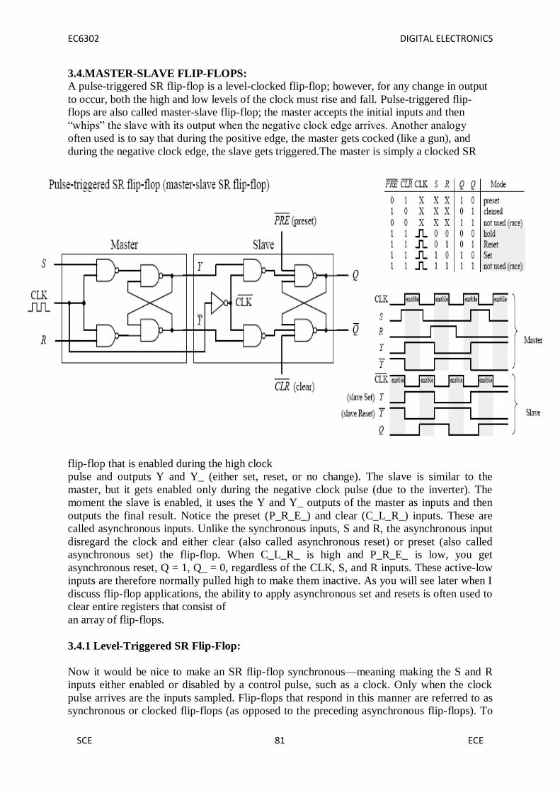
EC6302 DIGITAL ELECTRONICS
SCE 81 ECE
3.4.MASTER-SLAVE FLIP-FLOPS:
A pulse-triggered SR flip-flop is a level-clocked flip-flop; however, for any change in output
to occur, both the high and low levels of the clock must rise and fall. Pulse-triggered flip-
flops are also called master-slave flip-flop; the master accepts the initial inputs and then
“whips” the slave with its output when the negative clock edge arrives. Another analogy
often used is to say that during the positive edge, the master gets cocked (like a gun), and
during the negative clock edge, the slave gets triggered.The master is simply a clocked SR
flip-flop that is enabled during the high clock
pulse and outputs Y and Y_ (either set, reset, or no change). The slave is similar to the
master, but it gets enabled only during the negative clock pulse (due to the inverter). The
moment the slave is enabled, it uses the Y and Y_ outputs of the master as inputs and then
outputs the final result. Notice the preset (P_R_E_) and clear (C_L_R_) inputs. These are
called asynchronous inputs. Unlike the synchronous inputs, S and R, the asynchronous input
disregard the clock and either clear (also called asynchronous reset) or preset (also called
asynchronous set) the flip-flop. When C_L_R_ is high and P_R_E_ is low, you get
asynchronous reset, Q = 1, Q_ = 0, regardless of the CLK, S, and R inputs. These active-low
inputs are therefore normally pulled high to make them inactive. As you will see later when I
discuss flip-flop applications, the ability to apply asynchronous set and resets is often used to
clear entire registers that consist of
an array of flip-flops.
3.4.1 Level-Triggered SR Flip-Flop:
Now it would be nice to make an SR flip-flop synchronous—meaning making the S and R
inputs either enabled or disabled by a control pulse, such as a clock. Only when the clock
pulse arrives are the inputs sampled. Flip-flops that respond in this manner are referred to as
synchronous or clocked flip-flops (as opposed to the preceding asynchronous flip-flops). To

EC6302 DIGITAL ELECTRONICS
SCE 82 ECE
make the preceding SR flip-flop into a synchronous or clocked device, simply attach enable
gates to the inputs of the flip-flop, as shown in Fig.(Here, the cross-NAND arrangement is
used, though a cross-NOR arrangement also can be used.) Only when the clock is high are the
S and R inputs enabled. When the clock is low, the inputs are disabled, and the flip-flop is
placed in hold mode. The truth table and timing diagram below help illustrate how this device
works.
3.4.2 Ripple Counter (Asynchronous Counter) :

EC6302 DIGITAL ELECTRONICS
SCE 83 ECE
Asimple counter, called a MOD-16 ripple counter (or asynchronous counter), can be
constructed by joining four JK flop-flops together, as shown in Fig. (MOD-16, or modulus
16, means that the counter has 16 binary states.) This means that it can count from 0 to 15—
the zero is one of the counts. Each flip-flop in the ripple counter is fixed in toggle mode (J
and K are both held high). The clock signal applied to the first flip-flop causes the flip-flop to
divide the clock signal’s frequency by 2 at its Q0 output—a result of the toggle. The second
flip-flop receives Q0’s output at its clock input and likewise divides by 2. The process
continues down the line. What you get in the end is a binary counter with four digits. The
least significant bit (LSB) is Q0, while the most significant bit (MSB) is Q4. When the count
reaches 1111, the counter recycles back to 0000 and continues from there. To reset the
counter at any given time, the active-low clear line is pulsed low.To make the counter count
backward from 1111 to 0000, you would simply use the Q_ outputs.
The ripple counter above also can be used as a divide-by-2,4,8,16 counter. Here, you simply
replace the clock signal with any desired input signal that you wish to divide in frequency. To
get a divide-by-2 counter, you only need the first flip-flop; to get a divide-by-8 counter, you
need the first three flip-flops. Ripple counters with higher MOD values can be constructed by
slapping on more flip-flops to the MOD-16 counter. But how do you create a ripple counter
with a MOD value other than 2, 4, 8, 16, etc.? For example, say you want to create a MOD-
10 (0 to 9) ripple counter. Likewise, what do you do if you want to stop the counter after a
particular count has been reached and then trigger some device, such as an LED or buzzer.
The figure below shows just such a circuit.

EC6302 DIGITAL ELECTRONICS
SCE 84 ECE
To make a MOD-10 counter, you simply start with the MOD-16 counter and connect the Q0
and Q3 outputs to a NAND gate, as shown in the figure.When the counter reaches 9 (1001),
Q0 and Q3 will both go high, causing the NAND gate’s output to go low. The NAND gate
then sinks current, turning the LED on, while at the same time disabling the clock-enable gate
and stopping the count. (When the NAND gate is high, there is no potential difference across
the LED to light it up.) To start a new count, the active-low clear line is momentarily pulsed
low. Now, to make a MOD-15 counter, you would apply the same basic approach used to the
left, but you would connect Q1,Q2, and Q3 to a three-input NAND gate.
3.5 SYNCHRONOUS COUNTER:
There is a problem with the ripple counter just discussed. The output stages of the flip-flops
further down the line (from the first clocked flip-flop) take time to respond to changes that
occur due to the initial clock signal. This is a result of the internal propagation delay that
occurs within a given flip-flop.
A standard TTL flip-flop may have an internal propagation delay of 30 ns. If you join four
flip-flops to create a MOD-16 counter, the accumulative propagation delay at the highest-
order output will be 120 ns. When used in high-precision synchronous systems, such large
delays can lead to timing problems.
To avoid large delays, you can create what is called a synchronous counter. Synchronous
counters, unlike ripple (asynchronous) counters, contain flip-flops whose clock inputs are
driven at the same time by a common clock line. This means that output transitions for each
flip-flop will occur at the same time. Now, unlike the ripple counter, you must use some
additional logic circuitry placed between various flip-flop inputs and outputs to give the
desired count waveform.

EC6302 DIGITAL ELECTRONICS
SCE 85 ECE
For example, to create a 4-bit MOD-16 synchronous counter requires adding two additional
AND gates, as shown below. The AND gates act to keep a flip-flop in hold mode (if both
input of the gate are low) or toggle mode (if both inputs of the gate are high). So, during the
0–1 count, the first flip-flop is in toggle mode (and always is); all the rest are held in hold
mode. When it is time for the 2–4 count, the first and second flip-flops are placed in toggle
mode; the last two are held in hold mode.
When it is time for the 4–8 count, the first AND gate is enabled, allowing the the third flip-
flop to toggle. When it is time for the 8–15 count, the second AND gate is enabled, allowing
the last flip-flop to toggle. You can work out the details for yourself by studying the circuit
and timing waveforms.
The ripple (asynchronous) and synchronous counters discussed so far are simple but hardly
ever used. In practice, if you need a counter, be it ripple or synchronous, you go out and
purchase a counter IC. These ICs are often MOD-16 or MOD-10 counters and usually come
with many additional features. For example, many ICs allow you to preset the count to a
desired number via parallel input lines. Others allow you to count up or to count down by
means of control inputs. I will talk in great detail about counter ICs in a moment.
3.5.1SYNCHRONOUS UP /DOWN COUNTER:
The down counter counts in reverse from 1111 to 0000 and then goes to 1111. If we inspect
the count cycle, we find that each flip-flop will complement when the previous flip-flops are
all 0 (this is the opposite of the up counter). The down counter can be implemented similar to
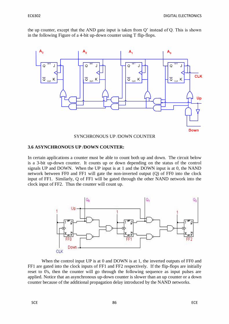
EC6302 DIGITAL ELECTRONICS
SCE 86 ECE
the up counter, except that the AND gate input is taken from Q’ instead of Q. This is shown
in the following Figure of a 4-bit up-down counter using T flip-flops.
SYNCHRONOUS UP /DOWN COUNTER
3.6 ASYNCHRONOUS UP /DOWN COUNTER:
In certain applications a counter must be able to count both up and down. The circuit below
is a 3-bit up-down counter. It counts up or down depending on the status of the control
signals UP and DOWN. When the UP input is at 1 and the DOWN input is at 0, the NAND
network between FF0 and FF1 will gate the non-inverted output (Q) of FF0 into the clock
input of FF1. Similarly, Q of FF1 will be gated through the other NAND network into the
clock input of FF2. Thus the counter will count up.
When the control input UP is at 0 and DOWN is at 1, the inverted outputs of FF0 and
FF1 are gated into the clock inputs of FF1 and FF2 respectively. If the flip-flops are initially
reset to 0's, then the counter will go through the following sequence as input pulses are
applied. Notice that an asynchronous up-down counter is slower than an up counter or a down
counter because of the additional propagation delay introduced by the NAND networks.

EC6302 DIGITAL ELECTRONICS
SCE 87 ECE
3.6.1 DESIGN OF SYNCHRONOUS COUNTERS:
This section begins our study of designing an important class of clocked sequential logic
circuits-synchronous finite-state machines. Like all sequential circuits, a finite-state machine
determines its outputs and its next state from its current inputs and current state. A
synchronous finite state machine changes state only on the clocking event.
COUNTER DESIGN PROCEDURE:
Describe a general sequential circuit in terms of its basic parts and its input and outputs.
Develop a state diagram for a given sequence. Develop a next-state table for a specific
counter sequence. Create a FF transition table. Use K-map to derive the logic equations.
Implement a counter to produce a specified sequence of states.
Design the 3-bit Gray code counter
Step 1: State Diagram
State Diagram for a 3-bit Gray code counter:
Step 2: Next-State Table
Next state table for a 3-bit Gray code counter

EC6302 DIGITAL ELECTRONICS
SCE 88 ECE
Step 3: Flip-Flop Transition Table
Transition table for a J-K Flip-Flop
Step 4: Karnaugh Maps
The following diagram shows the steps to create separate next states of
separate J and K from the current states of J and K.
Karnaugh maps for present-state J and K inputs for the 3-bit Gray code
counter..

EC6302 DIGITAL ELECTRONICS
SCE 89 ECE
Step 5: Logic Expressions for Flip-flop Inputs
The next-state J and K outputs for a 3-bit Gray code counter.
Step 6: Counter Implementation
The hardware diagram of the 3-bit Gray code counter
1. Design – Example 1
Design a counter with the irregular binary count sequence shown in the
state diagram of Figure 4.1.
Step 1: State Diagram

EC6302 DIGITAL ELECTRONICS
SCE 90 ECE
Step 2: Next-State Table
Step 3: Flip-Flop Transition Table
Transition table for a J-K Flip-Flop
Step 4: Karnaugh Maps
Step 5: Logic Expressions for Flip-flop Inputs
The expression for each J and K input taken from the maps is as follows:
J0 = 1, K0 = Q2

EC6302 DIGITAL ELECTRONICS
SCE 91 ECE
J1 = K1 = 1
J2 = K2 = Q1
Step 6: Counter Implementation
Example 2 - Design the 3 Up/down counter (Gray code sequence)
Step 1: State Diagram
Step 2: Next-State Table

EC6302 DIGITAL ELECTRONICS
SCE 92 ECE
.
Step 3: Flip-Flop Transition Table
Transition table for a J-K Flip-Flop
Here X denotes the don’t care condition Qn is the present state of transition output and
Qn+1 is the next state of the transition output
Step 4: Karnaugh Maps

EC6302 DIGITAL ELECTRONICS
SCE 93 ECE
Step 5: Logic Expressions for Flip-flop Inputs

EC6302 DIGITAL ELECTRONICS
SCE 94 ECE
Step 6: Counter Implementation
3.7.THE SHIFT REGISTER:
The Shift Register is another type of sequential logic circuit that is used for the storage or
transfer of data in the form of binary numbers and then "shifts" the data out once every clock
cycle, hence the name shift register. It basically consists of several single bit "D-Type Data
Latches", one for each bit (0 or 1) connected together in a serial or daisy-chain arrangement
so that the output from one data latch becomes the input of the next latch and so on. The data

EC6302 DIGITAL ELECTRONICS
SCE 95 ECE
bits may be fed in or out of the register serially, i.e. one after the other from either the left or
the right direction, or in parallel, i.e. all together. The number of individual data latches
required to make up a single Shift Register is determined by the number of bits to be stored
with the most common being 8-bits wide, i.e. eight individual data latches.
Shift Registers are used for data storage or data movement and are used in calculators or
computers to store data such as two binary numbers before they are added together, or to
convert the data from either a serial to parallel or parallel to serial format. The individual data
latches that make up a single shift register are all driven by a common clock (Clk) signal
making them synchronous devices. Shift register IC's are generally provided with a clear or
reset connection so that they can be "SET" or "RESET" as required.
Generally, shift registers operate in one of four different modes with the basic movement of
data through a shift register being:
Serial-in to Parallel-out (SIPO) - the register is loaded with serial data, one bit at a
time, with the stored data being available in parallel form.
Serial-in to Serial-out (SISO) - the data is shifted serially "IN" and "OUT" of the
register, one bit at a time in either a left or right direction under clock control.
Parallel-in to Serial-out (PISO) - the parallel data is loaded into the register
simultaneously and is shifted out of the register serially one bit at a time under clock
control.
Parallel-in to Parallel-out (PIPO) - the parallel data is loaded simultaneously into the
register, and transferred together to their respective outputs by the same clock pulse.
The effect of data movement from left to right through a shift register can be presented
graphically as:
Also, the directional movement of the data through a shift register can be either to the left,
(left shifting) to the right, (right shifting) left-in but right-out, (rotation) or both left and right
shifting within the same register thereby making it bidirectional. In this tutorial it is assumed
that all the data shifts to the right, (right shifting).

EC6302 DIGITAL ELECTRONICS
SCE 96 ECE
3.7.1.SERIAL-IN TO PARALLEL-OUT (SIPO)
4-bit Serial-in to Parallel-out Shift Register
The operation is as follows. Lets assume that all the flip-flops (FFA to FFD) have just been
RESET (CLEAR input) and that all the outputs QA to QD are at logic level "0" i.e, no parallel
data output. If a logic "1" is connected to the DATA input pin of FFA then on the first clock
pulse the output of FFA and therefore the resulting QA will be set HIGH to logic "1" with all
the other outputs still remaining LOW at logic "0". Assume now that the DATA input pin of
FFA has returned LOW again to logic "0" giving us one data pulse or 0-1-0.
The second clock pulse will change the output of FFA to logic "0" and the output of FFB and
QB HIGH to logic "1" as its input D has the logic "1" level on it from QA. The logic "1" has
now moved or been "shifted" one place along the register to the right as it is now at QA.
When the third clock pulse arrives this logic "1" value moves to the output of FFC (QC) and
so on until the arrival of the fifth clock pulse which sets all the outputs QA to QD back again
to logic level "0" because the input to FFA has remained constant at logic level "0".
The effect of each clock pulse is to shift the data contents of each stage one place to the right,
and this is shown in the following table until the complete data value of 0-0-0-1 is stored in
the register. This data value can now be read directly from the outputs of QA to QD. Then the
data has been converted from a serial data input signal to a parallel data output. The truth
table and following waveforms show the propagation of the logic "1" through the register
from left to right as follows.
Basic Movement of Data through a Shift Register
Clock Pulse No QA QB QC QD
0 0 0 0 0
1 1 0 0 0
2 0 1 0 0
3 0 0 1 0
4 0 0 0 1
5 0 0 0 0
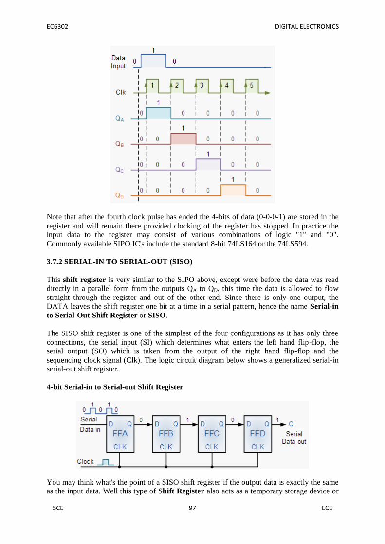
EC6302 DIGITAL ELECTRONICS
SCE 97 ECE
Note that after the fourth clock pulse has ended the 4-bits of data (0-0-0-1) are stored in the
register and will remain there provided clocking of the register has stopped. In practice the
input data to the register may consist of various combinations of logic "1" and "0".
Commonly available SIPO IC's include the standard 8-bit 74LS164 or the 74LS594.
3.7.2 SERIAL-IN TO SERIAL-OUT (SISO)
This shift register is very similar to the SIPO above, except were before the data was read
directly in a parallel form from the outputs QA to QD, this time the data is allowed to flow
straight through the register and out of the other end. Since there is only one output, the
DATA leaves the shift register one bit at a time in a serial pattern, hence the name Serial-in
to Serial-Out Shift Register or SISO.
The SISO shift register is one of the simplest of the four configurations as it has only three
connections, the serial input (SI) which determines what enters the left hand flip-flop, the
serial output (SO) which is taken from the output of the right hand flip-flop and the
sequencing clock signal (Clk). The logic circuit diagram below shows a generalized serial-in
serial-out shift register.
4-bit Serial-in to Serial-out Shift Register
You may think what's the point of a SISO shift register if the output data is exactly the same
as the input data. Well this type of Shift Register also acts as a temporary storage device or

EC6302 DIGITAL ELECTRONICS
SCE 98 ECE
as a time delay device for the data, with the amount of time delay being controlled by the
number of stages in the register, 4, 8, 16 etc or by varying the application of the clock pulses.
Commonly available IC's include the 74HC595 8-bit Serial-in/Serial-out Shift Register all
with 3-state outputs.
3.7.3 PARALLEL-IN TO SERIAL-OUT (PISO)
The Parallel-in to Serial-out shift register acts in the opposite way to the serial-in to parallel-
out one above. The data is loaded into the register in a parallel format i.e. all the data bits
enter their inputs simultaneously, to the parallel input pins PA to PD of the register. The data is
then read out sequentially in the normal shift-right mode from the register at Q representing
the data present at PA to PD. This data is outputted one bit at a time on each clock cycle in a
serial format. It is important to note that with this system a clock pulse is not required to
parallel load the register as it is already present, but four clock pulses are required to unload
the data.
4-bit Parallel-in to Serial-out Shift Register
As this type of shift register converts parallel data, such as an 8-bit data word into serial
format, it can be used to multiplex many different input lines into a single serial DATA
stream which can be sent directly to a computer or transmitted over a communications line.
Commonly available IC's include the 74HC166 8-bit Parallel-in/Serial-out Shift Registers.
3.7.4 PARALLEL-IN TO PARALLEL-OUT (PIPO)
The final mode of operation is the Parallel-in to Parallel-out Shift Register. This type of
register also acts as a temporary storage device or as a time delay device similar to the SISO
configuration above. The data is presented in a parallel format to the parallel input pins PA to
PD and then transferred together directly to their respective output pins QA to QA by the same
clock pulse. Then one clock pulse loads and unloads the register. This arrangement for
parallel loading and unloading is shown below.

EC6302 DIGITAL ELECTRONICS
SCE 99 ECE
4-bit Parallel-in to Parallel-out Shift Register
The PIPO shift register is the simplest of the four configurations as it has only three
connections, the parallel input (PI) which determines what enters the flip-flop, the parallel
output (PO) and the sequencing clock signal (Clk).
Similar to the Serial-in to Serial-out shift register, this type of register also acts as a
temporary storage device or as a time delay device, with the amount of time delay being
varied by the frequency of the clock pulses. Also, in this type of register there are no
interconnections between the individual flip-flops since no serial shifting of the data is
required.
3.8 UNIVERSAL SHIFT REGISTER
Today, high speed bi-directional "universal" type Shift Registers such as the TTL 74LS194,
74LS195 or the CMOS 4035 are available as a 4-bit multi-function devices that can be used
in either serial-to-serial, left shifting, right shifting, serial-to-parallel, parallel-to-serial, and as
a parallel-to-parallel multifunction data register, hence the name "Universal". These devices
can perform any combination of parallel and serial input to output operations but require
additional inputs to specify desired function and to pre-load and reset the device.
4-bit Universal Shift Register 74LS194

EC6302 DIGITAL ELECTRONICS
SCE 100 ECE
Universal shift registers are very useful digital devices. They can be configured to respond to
operations that require some form of temporary memory, delay information such as the SISO
or PIPO configuration modes or transfer data from one point to another in either a serial or
parallel format. Universal shift registers are frequently used in arithmetic operations to shift
data to the left or right for multiplication or division.
3.9.THE RING COUNTER:
In the previous Shift Register tutorial we saw that if we apply a serial data signal to the input
of a serial-in to serial-out shift register, the same sequence of data will exit from the last flip-
flip in the register chain after a preset number of clock cycles thereby acting as a sort of time
delay circuit to the original signal. But what if we were to connect the output of this shift
register back to its input so that the output from the last flip-flop, QD becomes the input of the
first flip-flop, DA. We would then have a closed loop circuit that "recirculates" the DATA
around a continuous loop for every state of its sequence, and this is the principal operation of
a Ring Counter. Then by looping the output back to the input, we can convert a standard
shift register into a ring counter. Consider the circuit below.
4-bit Ring Counter

EC6302 DIGITAL ELECTRONICS
SCE 101 ECE
The synchronous Ring Counter example above, is preset so that exactly one data bit in the
register is set to logic "1" with all the other bits reset to "0". To achieve this, a "CLEAR"
signal is firstly applied to all the flip-flops together in order to "RESET" their outputs to a
logic "0" level and then a "PRESET" pulse is applied to the input of the first flip-flop (FFA)
before the clock pulses are applied. This then places a single logic "1" value into the circuit of
the ring counter . On each successive clock pulse, the counter circulates the same data bit
between the four flip-flops over and over again around the "ring" every fourth clock cycle.
But in order to cycle the data correctly around the counter we must first "load" the counter
with a suitable data pattern as all logic "0"'s or all logic "1"'s outputted at each clock cycle
would make the ring counter invalid.
This type of data movement is called "rotation", and like the previous shift register, the effect
of the movement of the data bit from left to right through a ring counter .
Rotational Movement of a Ring Counter
Since the ring counter example shown above has four distinct states, it is also known as a
"modulo-4" or "mod-4" counter with each flip-flop output having a frequency value equal to
one-fourth or a quarter (1/4) that of the main clock frequency.
The "MODULO" or "MODULUS" of a counter is the number of states the counter counts or
sequences through before repeating itself and a ring counter can be made to output any

EC6302 DIGITAL ELECTRONICS
SCE 102 ECE
modulo number. A "mod-n" ring counter will require "n" number of flip-flops connected
together to circulate a single data bit providing "n" different output states. For example, a
mod-8 ring counter requires eight flip-flops and a mod-16 ring counter would require sixteen
flip-flops. However, as in our example above, only four of the possible sixteen states are
used, making ring counters very inefficient in terms of their output state usage.
3.10 JOHNSON RING COUNTER:
The Johnson Ring Counter or "Twisted Ring Counters", is another shift register with
feedback exactly the same as the standard Ring Counter above, except that this time the
inverted output Q of the last flip-flop is now connected back to the input D of the first flip-
flop as shown below. The main advantage of this type of ring counter is that it only needs
half the number of flip-flops compared to the standard ring counter then its modulo number is
halved. So a "n-stage" Johnson counter will circulate a single data bit giving sequence of 2n
different states and can therefore be considered as a "mod-2n counter".
4-bit Johnson Ring Counter
This inversion of Q before it is fed back to input D causes the counter to "count" in a
different way. Instead of counting through a fixed set of patterns like the normal ring counter
such as for a 4-bit counter, "0001"(1), "0010"(2), "0100"(4), "1000"(8) and repeat, the
Johnson counter counts up and then down as the initial logic "1" passes through it to the right
replacing the preceding logic "0". A 4-bit Johnson ring counter passes blocks of four logic
"0" and then four logic "1" thereby producing an 8-bit pattern. As the inverted output Q is
connected to the input D this 8-bit pattern continually repeats. For example, "1000", "1100",
"1110", "1111", "0111", "0011", "0001", "0000" and this is demonstrated in the following
table below.
Truth Table for a 4-bit Johnson Ring Counter
Clock Pulse No FFA FFB FFC FFD
0 0 0 0 0
1 1 0 0 0
2 1 1 0 0

EC6302 DIGITAL ELECTRONICS
SCE 103 ECE
3 1 1 1 0
4 1 1 1 1
5 0 1 1 1
6 0 0 1 1
7 0 0 0 1
As well as counting or rotating data around a continuous loop, ring counters can also be used
to detect or recognise various patterns or number values within a set of data. By connecting
simple logic gates such as the AND or the OR gates to the outputs of the flip-flops the circuit
can be made to detect a set number or value. Standard 2, 3 or 4-stage Johnson ring counters
can also be used to divide the frequency of the clock signal by varying their feedback
connections and divide-by-3 or divide-by-5 outputs are also available.
A 3-stage Johnson Ring Counter can also be used as a 3-phase, 120 degree phase shift square
wave generator by connecting to the data outputs at A, B and NOT-B. The standard 5-stage
Johnson counter such as the commonly available CD4017 is generally used as a synchronous
decade counter/divider circuit. The smaller 2-stage circuit is also called a "Quadrature"
(sine/cosine) Oscillator/Generator and is used to produce four individual outputs that are each
"phase shifted" by 90 degrees with respect to each other, and this is shown below.
2-bit Quadrature Generator
Output A B C D
QA+QB 1 0 0 0
QA+QB 0 1 0 0
QA+QB 0 0 1 0

EC6302 DIGITAL ELECTRONICS
SCE 104 ECE
QA+QB 0 0 0 1
2-bit Quadrature Oscillator, Count Sequence
As the four outputs, A to D are phase shifted by 90 degrees with regards to each other, they
can be used with additional circuitry, to drive a 2-phase full-step stepper motor for position
control or the ability to rotate a motor to a particular location as shown below.
Stepper Motor Control
2-phase (unipolar) Full-Step Stepper Motor Circuit
The speed of rotation of the Stepper Motor will depend mainly upon the clock frequency and
additional circuitry would be require to drive the "power" requirements of the motor. As this
section is only intended to give the reader a basic understanding of Johnson Ring Counters
and its applications, other good websites explain in more detail the types and drive
requirements of stepper motors.
Johnson Ring Counters are available in standard TTL or CMOS IC form, such as the
CD4017 5-Stage, decade Johnson ring counter with 10 active HIGH decoded outputs or the
CD4022 4-stage, divide-by-8 Johnson counter with 8 active HIGH decoded outputs.

EC6302 DIGITAL ELECTRONICS
SCE 105 ECE
UNIT 4 - MEMORY DEVICES
4.1. Classifications of Memory:
Many types of memory devices are available for use in modern computer systems. As an
embedded software engineer, you must be aware of the differences between them and
understand how to use each type effectively. In our discussion, we will approach these
devices from a software viewpoint. As you are reading, try to keep in mind that the
development of these devices took several decades. The names of the memory types
frequently reflect the historical nature of the development process.
Most software developers think of memory as being either RAM or ROM. But, in fact, there
are subtypes of each class, and even a third class of hybrid memories that exhibit some of the
characteristics of both RAM and ROM. In a RAM device, the data stored at each memory
location can be read or written, as desired. In a ROM device, the data stored at each memory
location can be read at will, but never written. The hybrid devices offer ROM-like
permanence, but under some conditions it is possible to overwrite their data provides a
classification system for the memory devices that are commonly found in embedded systems.
Common memory types in embedded systems
4.2 Types of RAM:
There are two important memory devices in the RAM family: SRAM and DRAM. The main
difference between them is the duration of the data stored. Static RAM (SRAM) retains its
contents as long as electrical power is applied to the chip. However, if the power is turned off
or lost temporarily, its contents will be lost forever. Dynamic RAM (DRAM), on the other
hand, has an extremely short data lifetimeusually less than a quarter of a second. This is true
even when power is applied continuously.
In short, SRAM has all the properties of the memory you think of when you hear the word
RAM. Compared with that, DRAM sounds kind of useless. What good is a memory device
that retains its contents for only a fraction of a second? By itself, such a volatile memory is
indeed worthless. However, a simple piece of hardware called a DRAM controller can be
used to make DRAM behave more like SRAM.The job of the DRAM controller, often
included within the processor, is to periodically refresh the data stored in the DRAM. By

EC6302 DIGITAL ELECTRONICS
SCE 106 ECE
refreshing the data several times a second, the DRAM controller keeps the contents of
memory alive for as long as they are needed. So, DRAM is as useful as SRAM after all.
When deciding which type of RAM to use, a system designer must consider access time and
cost. SRAM devices offer extremely fast access times (approximately four times faster than
DRAM) but are much more expensive to produce. Generally, SRAM is used only where
access speed is crucial. However, if a system requires only a small amount of memory,
SRAM may make more sense because you could avoid the cost of a DRAM controller.
A much lower cost-per-byte makes DRAM attractive whenever large amounts of RAM are
required. DRAM is also available in much larger capacities than SRAM. Many embedded
systems include both types: a small block of SRAM (a few hundred kilobytes) along a critical
data path and a much larger block of DRAM (in the megabytes) for everything else. Some
small embedded systems get by without any added memory: they use only the
microcontroller's on-chip memory.
4.3. Types of Rom:
Memories in the ROM family are distinguished by the methods used to write new data
to them (usually called programming or burning) and the number of times they can be
rewritten. This classification reflects the evolution of ROM devices from hardwired to one-
time programmable to erasable-and-programmable. A common feature across all these
devices is their ability to retain data and programs forever, even when power is removed.
The very first ROMs were hardwired devices that contained a preprogrammed set of
data or instructions. The contents of the ROM had to be specified before chip production, so
the actual data could be used to arrange the transistors inside the chip! Hardwired memories
are still used, though they are now called masked ROMs to distinguish them from other types
of ROM. The main advantage of a masked ROM is a low production cost. Unfortunately, the
cost is low only when hundreds of thousands of copies of the same ROM are required, and no
changes are ever needed.
Another type of ROM is the programmable ROM (PROM), which is purchased in an
unprogrammed state. If you were to look at the contents of an unprogrammed PROM, you
would see that all the bits are 1s. The process of writing your data to the PROM involves a
special piece of equipment called a device programmer, which writes data to the device by
applying a higher-than-normal voltage to special input pins of the chip. Once a PROM has
been programmed in this way, its contents can never be changed. If the code or data stored in
the PROM must be changed, the chip must be discarded and replaced with a new one. As a
result, PROMs are also known as one-time programmable (OTP) devices. Many small
embedded microcontrollers are also considered one-time programmable, because they contain
built-in PROM.
An erasable-and-programmable ROM (EPROM) is programmed in exactly the same
manner as a PROM. However, EPROMs can be erased and reprogrammed repeatedly. To
erase an EPROM, simply expose the device to a strong source of ultraviolet light. (There is a
"window" in the top of the device to let the ultraviolet light reach the silicon. You can buy an
EPROM eraser containing this light.) By doing this, you essentially reset the entire chip to its
initialunprogrammedstate. The erasure time of an EPROM can be anything from 10 to 45
minutes, which can make software debugging a slow process.

EC6302 DIGITAL ELECTRONICS
SCE 107 ECE
Though more expensive than PROMs, their ability to be reprogrammed made
EPROMs a common feature of the embedded software development and testing process for
many years. It is now relatively rare to see EPROMs used in embedded systems, as they have
been supplanted by newer technologies.
4.4 Hybrid Types:
As memory technology has matured in recent years, the line between RAM and ROM
devices has blurred. There are now several types of memory that combine the best features of
both. These devices do not belong to either group and can be collectively referred to as
hybrid memory devices. Hybrid memories can be read and written as desired, like RAM, but
maintain their contents without electrical power, just like ROM. Write cycles to hybrid
memories are similar to RAM, but they take significantly longer than writes to a RAM, so
you wouldn't want to use this type for your main system memory. Two of the hybrid devices,
EEPROM and flash, are descendants of ROM devices; the third, NVRAM, is a modified
version of SRAM.
An electrically-erasable-and-programmable ROM (EEPROM) is internally similar to
an EPROM, but with the erase operation accomplished electrically. Additionaly, a single byte
within an EEPROM can be erased and rewritten. Once written, the new data will remain in
the device foreveror at least until it is electrically erased. One tradeoff for this improved
functionality is higher cost; another is that typically EEPROM is good for 10,000 to 100,000
write cycles.
EEPROMs are available in a standard (address and data bus) parallel interface as well
as a serial interface. In many designs, the Inter-IC (I2C) or Serial Peripheral Interface (SPI)
buses are used to communicate with serial EEPROM devices. We'll take a look at the I2C and
SPI buses in Flash is the most important recent advancement in memory technology. It
combines all the best features of the memory devices described thus far. Flash memory
devices are high-density, low-cost, nonvolatile, fast (to read, but not to write), and electrically
reprogrammable. These advantages are overwhelming, and the use of flash memory has
increased dramatically in embedded systems as a direct result.
Erasing and writing data to a flash memory requires a specific sequence of writes
using certain data values. From a software viewpoint, flash and EEPROM technologies are
very similar. The major difference is that flash devices can be erased only one sector at a
time, not byte by byte. Typical sector sizes range from 8 KB to 64 KB. Despite this
disadvantage, flash is much more popular than EEPROM and is rapidly displacing many of
the ROM devices as well.
The third member of the hybrid memory class is nonvolatile RAM (NVRAM).
Nonvolatility is also a characteristic of the ROM and hybrid memories discussed earlier.
However, an NVRAM is physically very different from those devices. An NVRAM is
usually just an SRAM with a battery backup. When the power is on, the NVRAM operates
just like any other SRAM. But when the power is off, the NVRAM draws just enough
electrical power from the battery to retain its current contents. NVRAM is sometimes found
in embedded systems to store system-critical information. Incidentally, the "CMOS" in an
IBM-compatible PC was historically an NVRAM.

EC6302 DIGITAL ELECTRONICS
SCE 108 ECE
4.5. Programmable Logic Devices
PLD's are devices that can implement a wide variety of logic functions.
The programming may be permanent or reprogrammable.
Examples of common types of PROM's:
o ROM - (Read Only Memory) Is programmed by the manufacturer and can not
be altered by the user (you, the engineer).
o PROM -(Programmable ROM) can be programmed once. These are
programmed by frying a set of fuses in the device that permanently break
connections between wires. Thus, these devices can not be reprogrammed.
o EPROM - (Erasable PROM) can be programmed and reprogrammed. To
reprogram this device you have to put it under ultraviolet light for an extended
period of time.
o EEPROM - (Electricallly Erasable PROM) This device can be erased
electrically and is therefore much easier and quicker to work with than a
EPROM.
The other types of PLD's have similar technologies for programming them.
Common PLD's include:
o PROM's (I'll use this term generically to include all types of PROM's)
o PLA's - Programmable Array Logic. This technology is obsolete so I will not
discuss it.
o PAL Devices - Programmable Array Logic Devices. A very popular device for
implementing combinational logic, the type that we've been discussing.
o GAL Devices - Gate Array Logic. Similar to PAL Devices, but these have
additional flexibility.
o PGA - Programmable Gate Arrays. These are even more flexible than GAL's.
o FPGA's - Field Programmable Gate Arrays. These devices are very elaborate
and can be reprogrammed while being in complete system.
4.6 Programmable Logic Devices Logic devices constitute one of the three important classes of devices used to build digital
electronics systems, memory devices and microprocessors being the other two. Memory
devices such as ROM and RAM are used to store information such as the software
instructions of a program or the contents of a database, and microprocessors execute
software instructions to perform a variety of functions, from running a word-processing
program to carrying out far more complex tasks.
Logic devices implement almost every other function that the system must perform,
including device-to-device interfacing, data timing, control and display operations and so
on. So far, we have discussed those logic devices that perform fixed logic functions
decided upon at the manufacturing stage. Logic gates, multiplexers, demultiplexers,
arithmetic circuits, etc., are some examples. Sequential logic devices such as flip-flops,
counters, registers, etc., to be discussed in the following chapters, also belong to this
category of logic devices. In the present chapter, we will discuss a new category of
logic devices called programmable logic devices (PLDs).
The function to be performed by a programmable logic device is undefined at the time of
its manufacture. These devices are programmed by the user to perform a range of
functions depending upon the logic capacity and other features offered by the device.

EC6302 DIGITAL ELECTRONICS
SCE 109 ECE
We will begin with a comparison of fixed and programmable logic, and then follow
this up with a detailed description of different types of PLDs in terms of operational
fundamentals, salient features, architecture and typical applications. A brief
introduction to the devices offered by some of the major manufacturers of PLDs and
PLD programming languages is given towards the end of the chapter.
4.7 Fixed Logic Versus Programmable Logic
As outlined in the introduction, there are two broad categories of logic devices,
namely fixed logic devices and programmable logic devices. Whereas a fixed logic
device such as a logic gate or a multiplexer or a flip-flop performs a given logic
function that is known at the time of device manufacture, a programmable logic device
can be configured by the user to perform a large variety of logic functions. In terms of the
internal schematic arrangement of the two types of device, the circuits or building blocks
and their interconnections in a fixed logic device are permanent and cannot be altered
after the device is manufactured.
A programmable logic device offers to the user a wide range of logic capacity in
terms of digital building blocks, which can be configured by the user to perform the
intended function or set of functions. This configuration can be modified or altered any
number of times by the user by reprogramming the device. Figure shows a simple logic
circuit comprising four three-input AND gates and a four-input OR gate. This circuit
produces an output that is the sum output of a full adder. Here, A and B are the two bits
to be added, and C is the carry-in bit. It is a fixed logic device as the circuit is
unalterable from outside owing to fixed interconnections between the various building
blocks. Figure shows the logic diagram of a simple programmable device.
The device has an array of four six-input AND gates at the input and a four-
input OR gate at the output. Each AND gate can handle three variables and thus
can produce a product term of three variables.
The three variables (A, B and C in this case) or their complements can be
programmed to appear at the inputs of any of the four AND gates through fusible
links called antifuses. This means that each AND gate can produce the desired three-
variable product term. It may be mentioned here that an antifuse performs a function
that is opposite to that performed by a conventional electrical fuse.
A fuse has a low initial resistance and permanently breaks an electrically
conducting path when current through it exceeds a certain limiting value. In the case of
an antifuse, the initial resistance is very high and it is designed to create a low-
resistance electrically conducting path when voltage across it exceeds a certain level. As
a result, this circuit can be programmed to generate any three- variable sum-of-products
Boolean function having four minterms by activating the desired fusible links. For
example, the circuit could be programmed to produce the sum output resulting from the
addition of three bits (the sum output in the case of a full adder) or to produce
difference outputs resulting from subtraction of two bits with a borrow-in (the difference
output in the case of a full subtractor).

EC6302 DIGITAL ELECTRONICS
SCE 110 ECE
We can visualize that the logic circuit of Fig has a programmable AND array at the
input and a fixed OR gate at the output. Incidentally, this is the architecture of
programmable logic devices called programmable array logic (PAL). Practical PAL
devices have a much larger number of programmable AND gates and fixed OR gates to
have enhanced logic capacity and performance capability. PAL devices are discussed in
detail in the latter part of the chapter.
A B C
A
B
C Y
A B C
A
B
C
Fixed logic circuit.
A
B
C
+V
+V
Y
+V

EC6302 DIGITAL ELECTRONICS
SCE 111 ECE
Advantages and Disadvantages: 1. If we want to build a fixed logic device to perform a certain specific function, the time
required from design to the final stage when the manufactured device is actually
available for use could easily be several months to a year or so. PLD-based design
requires much less time from design cycle to production run.
2. In the case of fixed logic devices, the process of design validation followed by
incorporation of changes, if any, involves substantial nonrecurring engineering (NRE) costs,
which leads to an enhanced cost of the initial prototype device. In the case of PLDs,
inexpensive software tools can be used for quick validation of designs. The programmable
feature of these devices allows quick incorporation of changes and also a quick testing of the
device in an actual application environment.
In this case, the device used for prototyping is the same as the one that would qualify for
use in the end equipment.
3. In the case of programmable logic devices, users can change the circuit as
often as they want to until the design operates to their satisfaction. PLDs offer to the
users much more flexibility during the design cycle. Design iterations are nothing but
changes to the programming file.
4. Fixed logic devices have an edge for large-volume applications as they can be
mass produced more economically. They are also the preferred choice in
applications requiring the highest performance level.
4.8 Programmable Logic Devices – An Overview
There are many types of programmable logic device, distinguishable from one
another in terms of architecture, logic capacity, programmability and certain other
specific features. In this section, we will briefly discuss commonly used PLDs and their
salient features. A detailed description of each of them will follow in subsequent sections. 4.8.1 Programmable ROMs
PROM (Programmable Read Only Memory) and EPROM (Erasable
Programmable Read Only Memory) can be considered to be predecessors to PLDs. The
architecture of a programmable ROM allows the user to hardware-implement an arbitrary
combinational function of a given number of inputs. When used as a memory device, n
inputs of the ROM (called address lines in this case) and m outputs (called data lines) can
be used to store 2n m-bit words.
When used as a PLD, it can be used to implement m different combinational
functions, with each function being a chosen function of n variables. Any conceivable n-
variable Boolean function can be made to appear at any of the m output lines. A
generalized ROM device with n inputs and m outputs has 2n hard-wired AND gates at the
input and m programmable OR gates at the output. Each AND gate has n inputs, and each
OR gate has 2n inputs. Thus, each OR gate can be used to generate any conceivable
Boolean function of n variables, and this generalized ROM can be used to produce m
arbitrary n-variable Boolean functions.

EC6302 DIGITAL ELECTRONICS
SCE 112 ECE
The AND array produces all possible minterms of a given number of input variables,
and the programmable OR array allows only the desired minterms to appear at their inputs.
Figure shows the internal architecture
of a PROM having four input lines, a hard-wired array of 16 AND gates and a
programmable array of four OR gates.
A cross (×) indicates an intact (or unprogrammed) fusible link or interconnection, and
a dot (•) indicates a hard-wired interconnection. PROMs, EPROMs and EEPROMs
(Electrically Erasable Programmable Read Only Memory) can be programmed using
standard PROM programmers. One of the major disadvantages of PROMs is their inefficient
use of logic capacity. It is not economical to use PROMs for all those applications where
only a few minterms are needed.
Other disadvantages include relatively higher power consumption and an inability to
provide safe covers for asynchronous logic transitions. They are usually much slower than
the dedicated logic circuits. Also, they cannot be used to implement sequential logic owing
to the absence of flip-flops.
4.8.2 Programmable Logic Array
A programmable logic array (PLA) device has a programmable AND array
at the input and a programmable OR array at the output, which makes it one of the most
versatile PLDs. Its architecture differs from that of a PROM in the following respects. It
has a programmable AND array rather than a hard-wired AND array. The number of AND
gates in an m-input PROM is always equal to 2m . In the case of a PLA, the number of
AND gates in the programmable AND array for m input variables is usually much less
than 2m , and the number of inputs of each of the OR gates equals the number of AND
gates. Each OR gate can generate an arbitrary Boolean function with a maximum of
minterms equal to the number of AND gates. Figure 9.4 shows the internal architecture of
a PLA device with four input lines, a programmable array of eight AND gates at the input
and a programmable array of two OR gates at the output. A PLA device makes more
efficient use of logic capacity than a PROM. However, it has its own disadvantages
resulting from two sets of programmable fuses, which makes it relatively more difficult to
manufacture, program and test.
a GAL device can be erased and reprogrammed. Also, it has reprogrammable

EC6302 DIGITAL ELECTRONICS
SCE 113 ECE
output logic. This feature makes it particularly attractive at the device
prototyping stage, as any bugs in the logic can be corrected by reprogramming.
A similar device called PEEL (Programmable Electrically Erasable Logic) was
introduced by the International CMOS Technology (ICT) Corporation.
4.8.5 Complex Programmable Logic Device
Programmable logic devices such as PLAs, PALs, GALs and other PAL-like devices
are often grouped into a single category called simple programmable logic devices (SPLDs)
to distinguish them from the ones that are far more complex.
A complex programmable logic device (CPLD), as the name suggests, is a much
more complex device than any of the programmable logic devices discussed so far. A
CPLD may contain circuitry equivalent to that of several PAL devices linked to each other
by programmable interconnections. Figure shows the internal structure of a typical
CPLD. Each of the four logic blocks is equivalent to a PLD such as a PAL device.
The number of logic blocks in a CPLD could be more or less than four. Each of the
logic blocks has programmable interconnections. A switch matrix is used for logic block
to logic block interconnections. Also, the switch matrix in a CPLD may or may not
be fully connected. That is, some of the possible connections between logic block outputs
and inputs may not be supported by a given CPLD.
While the complexity of a typical PAL device may be of the order of a few hundred
logic gates, a CPLD may have a complexity equivalent to tens of thousands of logic gates.
When compared with FPGAs, CPLDs offer predictable timing characteristics owing to
their less flexible internal architecture and are thus ideal for critical control applications and
other applications where a high performance level is required. Also, because of their
relatively much lower power consumption and lower cost, CPLDs are an ideal solution for
battery-operated portable applications such as mobile phones, digital assistants and so on.
A CPLD can be programmed either by using a PAL programmer or by feeding it
with a serial data stream from a PC after soldering it on the PC board. A circuit on the
CPLD decodes the data stream and configures it to perform the intended logic function. 4.8.6 Field-Programmable Gate Array
A field-programmable gate array (FPGA) uses an array of logic blocks, which can
be configured by the user. The term ‘field-programmable’ here signifies that the
device is programmable outside the factory where it is manufactured. The internal
architecture of an FPGA device has three main parts, namely the array of logic blocks, the
programmable interconnects and the I/O blocks.
Figure shows the architecture of a typical FPGA. Each of the I/O blocks provides an
individually selectable input, output or bidirectional access to one of the general-purpose
I/O pins on the FPGA package. The logic blocks in an FPGA are no more complex
than a couple of logic gates or a look-up table feeding a flip-flop. The programmable
interconnects connect logic blocks to logic blocks and also I/O blocks to logic blocks.
FPGAs offer a much higher logic density and much larger performance features
compared with CPLDs. Some of the contemporary FPGA devices offer a logic

EC6302 DIGITAL ELECTRONICS
SCE 114 ECE
complexity equivalent to that of eight million system gates. Also, these devices offer
features such as built-in hard-wired processors,
Programmable Interconnect
I/O Blocks
Logic Blocks
FPGA Architecture large memory, clock management systems and support for many of the contemporary device-to- device signalling technologies. FPGAs find extensive use in a variety of applications, which include data processing and storage, digital signal processing, instrumentation and telecommunications
4.9Memory Hierarchy
Introduction
• Memory unit is an essential component in any digital computer as it is needed for
storing programs and data.
• A computer is equipped with a hierarchy of memory subsystems, some internal to the
system (directly accessible by the processor), and some external (accessible by the
processor via an I/O module)
• External memory consists of peripheral storage devices, such as disk and tape, that
are accessible to the CPU via I/O controllers. External memory can also be referred as
secondary memory or auxiliary memory.
• Internal memory is equated with main memory. But there are other forms of internal
memory like CPU requires its own local memory in the form of registers. Internal
memory is also called as main memory/Primary memory.

EC6302 DIGITAL ELECTRONICS
SCE 115 ECE
Main memory can be classified as
1) Volatile: -- RAM (Random Access Memory)
-- RAM is working memory. Data can be read or written in RAM with the help of
address location and when the data is no longer needed we can use the storage
location for writing again.
-- Contents of volatile memory are vanished when power supply is switched off.
2) Non Volatile :
-- ROM (Read Only Memory)
-- It is useful to have instructions that are used often , permanently stored inside the
computer. Programs and data on the ROM are not lost if the computer is powered down
There are three key characteristics of memory:
• COST
• CAPACITY
• ACCESS TIME
The relationship between them is as follows:
Greater capacity, smaller cost per bit
Greater capacity, greater access time
Smaller access time, greater cost per bit
The overall goal of using a memory hierarchy is to obtain the highest possible average
access speed while minimizing total cost of entire memory system.

EC6302 DIGITAL ELECTRONICS
SCE 116 ECE
4.10Random-Access Memory (RAM)
• Key features
– RAM is packaged as a chip.
– Basic storage unit is a cell (one bit per cell).
– Multiple RAM chips form a memory.
– It is possible to both read data from and write data to memory easily and
rapidly.
– Two additional forms of RAM are as follows…
• Static RAM (SRAM)
– Each cell stores bit with inverter, transistor circuit.
– Retains value indefinitely, as long as it is kept powered.
– Relatively insensitive to disturbances such as electrical noise.
– Faster and more expensive than DRAM.
– Access time is about 10 ns
Memory hierarchy
L0:
L1:
L2:
L3:
L4:
Registers
Cache
Magnetic disk
Magnetic tape
Main Memory
Larger,
slower,
and
cheaper
(per byte)
Smaller,
faster,
and
costlier
(per byte)

EC6302 DIGITAL ELECTRONICS
SCE 117 ECE
– Used for cache memory
• Dynamic RAM (DRAM)
– Each cell stores bit with a capacitor and transistor.
– Because the capacitors have a natural tendency to discharge, value must be
refreshed every 10-100 ms.
– Sensitive to disturbances.
– Slower and cheaper than SRAM.
– Read and write operations are suspended when the refresh cycle is going on,
this increases the effective access time to 50ns.
– Used for main memory
Advanced DRAM Organization
• Enhanced DRAM
• Cache DRAM
• Synchronous DRAM
• Rambus DRAM
• Enhanced DRAM
Simplest of new DRAM architectures
Developed by Ramtron
Integrates a small SRAM cache onto a DRAM chip
Refresh operation can be conducted in parallel with cache read operation
It has separate read path and write path so it enables a subsequent read access
to cache in parallel with the completion of write operation.
• Cache DRAM
Developed by Mitsubishi
Similar to EDRAM, includes a larger SRAM cache than the EDRAM
SRAM on CDRAM can be used as either true cache or as a buffer to support
the serial access to a block of data.
Buffer stores most recently accessed data.
• Synchronous DRAM
Jointly developed by no of companies
It exchanges data with the processor synchronized to an external clock signal
It runs at speed equivalent to that of processor/memory bus without imposing
wait states.
Data moves in and out from DRAM under the control of system clock.
It has dual bank internal architecture
SDRAM includes important key features like Mode register and associated
control logic. It provides a mechanism to customize SDRAM according to
system needs.
It performs best when transferring large blocks of data serially, e.g. in word
processing, multimedia etc.
• Rambus DRAM
Developed by Rambus
RDRAM chips are vertical packages, with all pins on one side.
fastest current memory technologies used by PCs. Normally SRAM can
deliver data at a maximum speed of about 100 MHz, RDRAM transfers data at
up to 800 MHz
RDRAM is used with Pentium III Xeon processors and more recently it is
being used with Pentium 4 processors.

EC6302 DIGITAL ELECTRONICS
SCE 118 ECE
4.11 MEMORY DETAILS:

EC6302 DIGITAL ELECTRONICS
SCE 119 ECE
UNIT 5 - SYNCHRONOUS AND ASYNCHRONOUS SEQUENTIAL CIRCUITS
5.1 INTRODUCTION
Digital electronics is classified into combinational logic and sequential logic.
Combinational logic output depends on the inputs levels, whereas sequential logic output
depends on stored levels and also the input levels.
The memory elements are devices capable of storing binary info. The binary info
stored in the memory elements at any given time defines the state of the sequential circuit.
The input and the present state of the memory element determines the output. Memory
elements next state is also a function of external inputs and present state. A sequential circuit
is specified by a time sequence of inputs, outputs, and internal states.
There are two types of sequential circuits. Their classification depends on the timing of
their signals:
Asynchronous sequential circuits
synchronous sequential circuits
5.2 SYNCHRONOUS SEQUENTIAL CIRCUIT
This type of system uses storage elements called flip-flops that are employed to
change their binary value only at discrete instants of time. Synchronous sequential circuits
use logic gates and flip-flop storage devices. Sequential circuits have a clock signal as one of
their inputs. All state transitions in such circuits occur only when the clock value is either 0 or
1 or happen at the rising or falling edges of the clock depending on the type of memory
elements used in the circuit. Synchronization is achieved by a timing device called a clock
pulse generator. Clock pulses are distributed throughout the system in such a way that the
flip-flops are affected only with the arrival of the synchronization pulse. Synchronous
sequential circuits that use clock pulses in the inputs are called clocked-sequential circuits.
They are stable and their timing can easily be broken down into independent discrete steps,
each of which is considered separately.

EC6302 DIGITAL ELECTRONICS
SCE 120 ECE
A clock signal is a periodic square wave that indefinitely switches from 0 to 1 and
from 1 to 0 at fixed intervals. Clock cycle time or clock period: the time interval between two
consecutive rising or falling edges of the clock.
Clock Frequency = 1 / clock cycle time (measured in cycles per second or Hz)
Example: Clock cycle time = 10ns clock frequency = 100M
5.3 CONCEPT OF SEQUENTIAL LOGIC
A sequential circuit as seen in the last page, is combinational logic with some
feedback to maintain its current value, like a memory cell. To understand the basics let's
consider the basic feedback logic circuit below, which is a simple NOT gate whose output is
connected to its input. The effect is that output oscillates between HIGH and LOW (i.e. 1 and
0). Oscillation frequency depends on gate delay and wire delay. Assuming a wire delay of 0
and a gate delay of 10ns, then oscillation frequency would be (on time + off time = 20ns)
50Mhz.
The basic idea of having the feedback is to store the value or hold the value, but in the
above circuit, output keeps toggling. We can overcome this problem with the circuit below,
which is basically cascading two inverters, so that the feedback is in-phase, thus avoids
toggling. The equivalent circuit is the same as having a buffer with its output connected to its
input.

EC6302 DIGITAL ELECTRONICS
SCE 121 ECE
But there is a problem here too: each gate output value is stable, but what will it be?
Or in other words buffer output can not be known. There is no way to tell. If we could know
or set the value we would have a simple 1-bit storage/memory element.
The circuit below is the same as the inverters connected back to back with provision to set the
state of each gate (NOR gate with both inputs shorted is like a inverter). I am not going to
explain the operation, as it is clear from the truth table. S is called set and R is called Reset.
S R Q Q+
0 0 0 0
0 0 1 1
0 1 X 0
1 0 X 1
1 1 X 0
There still seems to be some problem with the above configuration, we can not control when
the input should be sampled, in other words there is no enable signal to control when the
input is sampled. Normally input enable signals can be of two types.
Level sensitive or (Latch)
Edge Sensitive or (Flip-Flop)
5.3.1 Level Sensitive
The circuit below is a modification of the above one to have level sensitive enable
input. Enable, when LOW, masks the input S and R. When HIGH, presents S and R to the
sequential logic input (the above circuit two NOR Gates). Thus Enable, when HIGH,
transfers input S and R to the sequential cell transparently, so this kind of sequential circuits
are called transparent Latch. The memory element we get is an RS Latch with active high
Enable.

EC6302 DIGITAL ELECTRONICS
SCE 122 ECE
5.3.2 Edge Sensitive
The circuit below is a cascade of two level sensitive memory elements, with a phase
shift in the enable input between first memory element and second memory element. The first
RS latch (i.e. the first memory element) will be enabled when CLK input is HIGH and the
second RS latch will be enabled when CLK is LOW. The net effect is input RS is moved to Q
and Q' when CLK changes state from HIGH to LOW, this HIGH to LOW transition is called
falling edge. So the Edge Sensitive element we get is called negative edge RS flip-flop.
Now that we know the sequential circuits basics, let's look at each of them in detail in
accordance to what is taught in colleges. You are always welcome to suggest if this can be
written better in any way.
5.4 LATCHES AND FLIP-FLOPS
There are two types of sequential circuits.
Synchronous Circuits.
Asynchronous Circuits.
As seen in last section, Latches and Flip-flops are one and the same with a slight
variation: Latches have level sensitive control signal input and Flip-flops have edge sensitive
control signal input. Flip-flops and latches which use this control signals are called
synchronous circuits. So if they don't use clock inputs, then they are called asynchronous
circuits.
5.4.1 RS Latch
RS latch have two inputs, S and R. S is called set and R is called reset. The S input is
used to produce HIGH on Q ( i.e. store binary 1 in flip-flop). The R input is used to produce
LOW on Q (i.e. store binary 0 in flip-flop). Q' is Q complementary output, so it always holds
the opposite value of Q. The output of the S-R latch depends on current as well as previous
inputs or state, and its state (value stored) can change as soon as its inputs change. The circuit
and the truth table of RS latch is shown below.

EC6302 DIGITAL ELECTRONICS
SCE 123 ECE
S R Q Q+
0 0 0 0
0 0 1 1
0 1 X 0
1 0 X 1
1 1 X 0
The operation has to be analyzed with the 4 inputs combinations together with the 2 possible
previous states.
When S = 0 and R = 0: If we assume Q = 1 and Q' = 0 as initial condition, then output
Q after input is applied would be Q = (R + Q')' = 1 and Q' = (S + Q)' = 0. Assuming Q
= 0 and Q' = 1 as initial condition, then output Q after the input applied would be Q =
(R + Q')' = 0 and Q' = (S + Q)' = 1. So it is clear that when both S and R inputs are
LOW, the output is retained as before the application of inputs. (i.e. there is no state
change).
When S = 1 and R = 0: If we assume Q = 1 and Q' = 0 as initial condition, then output
Q after input is applied would be Q = (R + Q')' = 1 and Q' = (S + Q)' = 0. Assuming Q
= 0 and Q' = 1 as initial condition, then output Q after the input applied would be Q =
(R + Q')' = 1 and Q' = (S + Q)' = 0. So in simple words when S is HIGH and R is
LOW, output Q is HIGH.
When S = 0 and R = 1: If we assume Q = 1 and Q' = 0 as initial condition, then output
Q after input is applied would be Q = (R + Q')' = 0 and Q' = (S + Q)' = 1. Assuming Q
= 0 and Q' = 1 as initial condition, then output Q after the input applied would be Q =
(R + Q')' = 0 and Q' = (S + Q)' = 1. So in simple words when S is LOW and R is
HIGH, output Q is LOW.
When S = 1 and R =1 : No matter what state Q and Q' are in, application of 1 at input
of NOR gate always results in 0 at output of NOR gate, which results in both Q and Q'
set to LOW (i.e. Q = Q'). LOW in both the outputs basically is wrong, so this case is
invalid.
It is possible to construct the RS latch using NAND gates (of course as seen in Logic
gates section). The only difference is that NAND is NOR gate dual form (Did I say that in

EC6302 DIGITAL ELECTRONICS
SCE 124 ECE
Logic gates section?). So in this case the R = 0 and S = 0 case becomes the invalid case. The
circuit and Truth table of RS latch using NAND is shown below.
S R Q Q+
1 1 0 0
1 1 1 1
0 1 X 0
1 0 X 1
0 0 X 1
If you look closely, there is no control signal (i.e. no clock and no enable), so this kind of
latches or flip-flops are called asynchronous logic elements. Since all the sequential circuits
are built around the RS latch, we will concentrate on synchronous circuits and not on
asynchronous circuits.
5.4.2 RS Latch with Clock
We have seen this circuit earlier with two possible input configurations: one with
level sensitive input and one with edge sensitive input. The circuit below shows the level
sensitive RS latch. Control signal "Enable" E is used to gate the input S and R to the RS
Latch. When Enable E is HIGH, both the AND gates act as buffers and thus R and S appears
at the RS latch input and it functions like a normal RS latch. When Enable E is LOW, it
drives LOW to both inputs of RS latch. As we saw in previous page, when both inputs of a
NOR latch are low, values are retained (i.e. the output does not change).

EC6302 DIGITAL ELECTRONICS
SCE 125 ECE
5.4.2.1 Set up and Hold time
For synchronous flip-flops, we have special requirements for the inputs with respect
to clock signal input. They are
Setup Time: Minimum time period during which data must be stable before the clock
makes a valid transition. For example, for a posedge triggered flip-flop, with a setup
time of 2 ns, Input Data (i.e. R and S in the case of RS flip-flop) should be stable for
at least 2 ns before clock makes transition from 0 to 1.
Hold Time: Minimum time period during which data must be stable after the clock
has made a valid transition. For example, for a posedge triggered flip-flop, with a hold
time of 1 ns. Input Data (i.e. R and S in the case of RS flip-flop) should be stable for
at least 1 ns after clock has made transition from 0 to 1.
If data makes transition within this setup window and before the hold window, then
the flip-flop output is not predictable, and flip-flop enters what is known as meta stable state.
In this state flip-flop output oscillates between 0 and 1. It takes some time for the flip-flop to
settle down. The whole process is called metastability. You could refer to tidbits section to
know more information on this topic.
The waveform below shows input S (R is not shown), and CLK and output Q (Q' is not
shown) for a SR posedge flip-flop.
5.4.3 D Latch
The RS latch seen earlier contains ambiguous state; to eliminate this condition we can
ensure that S and R are never equal. This is done by connecting S and R together with an
inverter. Thus we have D Latch: the same as the RS latch, with the only difference that there
is only one input, instead of two (R and S). This input is called D or Data input. D latch is
called D transparent latch for the reasons explained earlier. Delay flip-flop or delay latch is
another name used. Below is the truth table and circuit of D latch.
In real world designs (ASIC/FPGA Designs) only D latches/Flip-Flops are used.

EC6302 DIGITAL ELECTRONICS
SCE 126 ECE
D Q Q+
1 X 1
0 X 0
Below is the D latch waveform, which is similar to the RS latch one, but with R
removed.
5.4.4 JK Latch
The ambiguous state output in the RS latch was eliminated in the D latch by joining
the inputs with an inverter. But the D latch has a single input. JK latch is similar to RS latch
in that it has 2 inputs J and K as shown figure below. The ambiguous state has been
eliminated here: when both inputs are high, output toggles. The only difference we see here is
output feedback to inputs, which is not there in the RS latch.

EC6302 DIGITAL ELECTRONICS
SCE 127 ECE
J K Q
1 1 0
1 1 1
1 0 1
0 1 0
5.4.5 T Latch
When the two inputs of JK latch are shorted, a T Latch is formed. It is called T latch as, when
input is held HIGH, output toggles.
T Q Q+
1 0 1
1 1 0
0 1 1
0 0 0

EC6302 DIGITAL ELECTRONICS
SCE 128 ECE
5.4.6 JK Master Slave Flip-Flop
All sequential circuits that we have seen in the last few pages have a problem (All
level sensitive sequential circuits have this problem). Before the enable input changes state
from HIGH to LOW (assuming HIGH is ON and LOW is OFF state), if inputs changes, then
another state transition occurs for the same enable pulse. This sort of multiple transition
problem is called racing.
If we make the sequential element sensitive to edges, instead of levels, we can
overcome this problem, as input is evaluated only during enable/clock edges.
In the figure above there are two latches, the first latch on the left is called master
latch and the one on the right is called slave latch. Master latch is positively clocked and
slave latch is negatively clocked.
5.5 SEQUENTIAL CIRCUITS DESIGN PROCEDURES
We saw in the combinational circuits section how to design a combinational circuit from
the given problem. We convert the problem into a truth table, then draw K-map for the truth
table, and then finally draw the gate level circuit for the problem. Similarly we have a flow
for the sequential circuit design. The steps are given below.
Draw state diagram.
Draw the state table (excitation table) for each output.
Draw the K-map for each output.
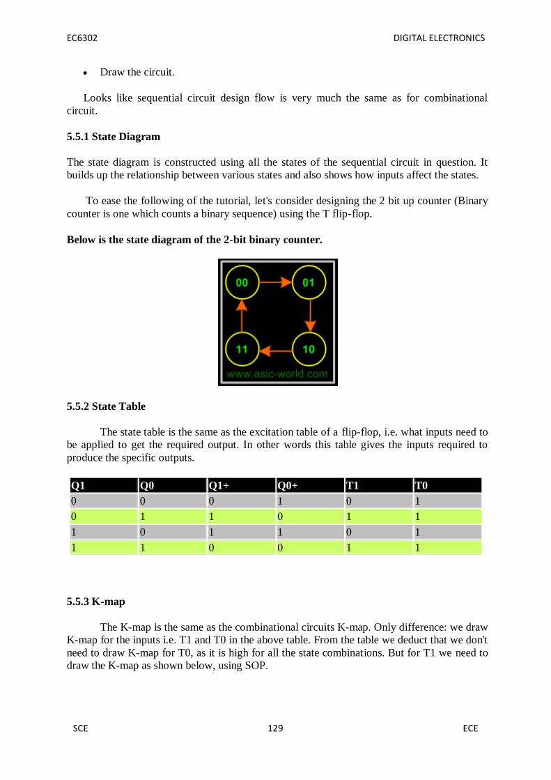
EC6302 DIGITAL ELECTRONICS
SCE 129 ECE
Draw the circuit.
Looks like sequential circuit design flow is very much the same as for combinational
circuit.
5.5.1 State Diagram
The state diagram is constructed using all the states of the sequential circuit in question. It
builds up the relationship between various states and also shows how inputs affect the states.
To ease the following of the tutorial, let's consider designing the 2 bit up counter (Binary
counter is one which counts a binary sequence) using the T flip-flop.
Below is the state diagram of the 2-bit binary counter.
5.5.2 State Table
The state table is the same as the excitation table of a flip-flop, i.e. what inputs need to
be applied to get the required output. In other words this table gives the inputs required to
produce the specific outputs.
Q1 Q0 Q1+ Q0+ T1 T0
0 0 0 1 0 1
0 1 1 0 1 1
1 0 1 1 0 1
1 1 0 0 1 1
5.5.3 K-map
The K-map is the same as the combinational circuits K-map. Only difference: we draw
K-map for the inputs i.e. T1 and T0 in the above table. From the table we deduct that we don't
need to draw K-map for T0, as it is high for all the state combinations. But for T1 we need to
draw the K-map as shown below, using SOP.
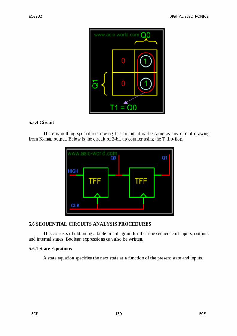
EC6302 DIGITAL ELECTRONICS
SCE 130 ECE
5.5.4 Circuit
There is nothing special in drawing the circuit, it is the same as any circuit drawing
from K-map output. Below is the circuit of 2-bit up counter using the T flip-flop.
5.6 SEQUENTIAL CIRCUITS ANALYSIS PROCEDURES
This consists of obtaining a table or a diagram for the time sequence of inputs, outputs
and internal states. Boolean expressions can also be written.
5.6.1 State Equations
A state equation specifies the next state as a function of the present state and inputs.

EC6302 DIGITAL ELECTRONICS
SCE 131 ECE
Consider the following sequential circuit:
Since the D input of a flip-flop determines the value of the next state, the equations for the
next state are:
A(t+1) = A(t) x(t) + B(t) x(t)
B(t+1) = A’(t) x(t)
The left-side of each equation denotes the next state of the flip-flop and the right-side
specifies the present state and the conditions that make the next state equal to 1. These can be
expressed in a more compact form by omitting the (t):

EC6302 DIGITAL ELECTRONICS
SCE 132 ECE
A(t+1) = Ax + Bx
B(t+1) = A’x
The present state value of the output can be expressed as:
y(t) =[A(t) + B(t)]x’(t)
The above output equation can be expressed in a more compact form as:
y = (A + B)x’
5.6.2 State Table
The time sequence of inputs, outputs, and flip-flop states can be enumerated in a state
table. This can be generated from the logic diagram or the state equations.
Two alternative forms for the sequential circuit shown previously are as follows:
5.6.3 State Diagram
The information available in a state table can be represented graphically in a form of a
state diagram. In this diagram, a state is represented by a circle, and the transitions between
states by directed lines connecting the circles:

EC6302 DIGITAL ELECTRONICS
SCE 133 ECE
Each directed lines are labelled with two binary numbers separated by a slash. The
input value during the present state is labelled first, and the number after the slash gives the
output during the present state with the given input. A directed line connecting a circle with
itself indicates that no change of state occurs.
5.6.4 Flip-Flop Input Equations
These fully specify the combinational logic that drives the flip-flops and they imply
the type of flipflop from the letter symbol. The input equations for the circuit analysed before
and shown below are:

EC6302 DIGITAL ELECTRONICS
SCE 134 ECE
For a D flip-flop, the state equation is the same as the input equation. Input equations
are sometimes called excitation equations.
5.7 ANALYSIS WITH D FLIP-FLOPS
Example: Analyze the clocked sequential circuit described by the input equation:
DA = A x y
Solution:
The DA symbol implies a D flip-flop with output A. The x and y variables are the
inputs to the circuit. Since no output equations are given, the output is implied to come from
the output of the flip-flop.The next state values are obtained from the state equation:
A(t+1) = A x y

EC6302 DIGITAL ELECTRONICS
SCE 135 ECE
5.8 ANALYSIS WITH JK FLIP-FLOPS
The next state values of a sequential circuit that uses JK or T flip-flops can be derived
from:
A) the characteristic table, or
B) the characteristic equation.
Procedure:
Determine the flip-flop input equations in terms of the present state and input
variables.
List the binary values of each equation.
Use the flip-flop characteristic table to find the next state values in the state
table.
As an example consider the following circuit:

EC6302 DIGITAL ELECTRONICS
SCE 136 ECE
The circuit can be specified by the flip-flop input equations:
JA = B KA = BX’
JB = X’ KB = A’X + AX’
The state table is:
The next state of each flip-flop is determined from the corresponding J and K inputs
and the characteristic table of the JK flip-flop listed below:

EC6302 DIGITAL ELECTRONICS
SCE 137 ECE
5.9 ANALYSIS WITH T FLIP-FLOPS
As with JK flip-flops, the next state values can be obtained either by using the characteristic
table:
or by the characteristic equation:
Q(t+1) = T Q
Consider the following sequential circuit:
It can be described algebraically by two input equations and an output equation:
TA = BX TB = X y = AB

EC6302 DIGITAL ELECTRONICS
SCE 138 ECE
The state table for this circuit is listed below:
The values for y are obtained from the output equation. The values for the next state
can be derived from the state equations by substituting TA and TB in the characteristic
equations, yielding:
A(t+1) = (BX)’A + (BX)A’ = AB’ + AX’ + A’BX
B(t+1) = X B
The state diagram for the circuit is shown below:
As long as input x is equal to 1, the circuit behaves as a binary counter with a
sequence of states 00, 01, 10, 11, and back to 00.
When x = 0, the circuit remains in the same state. Output y is equal to 1 when the
present state is 11. The output depends on the present state only and is independent of the
input.
The two values inside each circle separated by a slash are for the present state and
output.

EC6302 DIGITAL ELECTRONICS
SCE 139 ECE
5.10 MEALY AND MOORE MODELS
The most general model of a sequential circuit has inputs, outputs and internal states. It is
common to distinguish between two models of sequential circuits:
Mealy model – The output is a function of both the present state and input.
Moore model – The output is a function of the present state only.
An example of a Mealy model is:
An example of a Moore model is:

EC6302 DIGITAL ELECTRONICS
SCE 140 ECE
In a Moore model, the outputs of the sequential circuit are synchronized with the
clock because they depend on only flip-flop outputs that are synchronized with the clock
In a Mealy model, the outputs may change if the inputs change during the clock cycle.
To achieve synchronization, the inputs must be synchronized with the clock and the outputs
must be sampled only during the clock edge.
5.11 STATE REDUCTION & ASSIGNMENT
Sometimes certain properties of sequential circuits may be used to reduce the number
of gates and flip-flops during the design.
The problem of state reduction is to find ways of reducing the number of states in a
sequential circuit, while keeping the external input-output relationships unchanged.
For example, suppose a sequential circuit is specified by the following seven-state
diagram:
There are an infinite number of input sequences that may be applied; each results in a
unique output sequence. Consider the input sequence 01010110100 starting from the initial
state a:
An algorithm for the state reduction quotes that:
“Two states are said to be equivalent if, for each member of the set of inputs, they
give exactly the same output and send the circuit either to the same state or to an equivalent
state.”
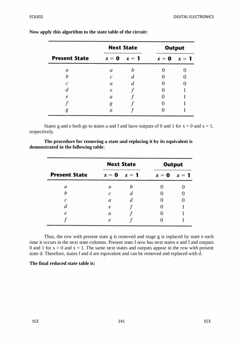
EC6302 DIGITAL ELECTRONICS
SCE 141 ECE
Now apply this algorithm to the state table of the circuit:
States g and e both go to states a and f and have outputs of 0 and 1 for x = 0 and x = 1,
respectively.
The procedure for removing a state and replacing it by its equivalent is
demonstrated in the following table:
Thus, the row with present state g is removed and stage g is replaced by state e each
time it occurs in the next state columns. Present state f now has next states e and f and outputs
0 and 1 for x = 0 and x = 1. The same next states and outputs appear in the row with present
state d. Therefore, states f and d are equivalent and can be removed and replaced with d.
The final reduced state table is:

EC6302 DIGITAL ELECTRONICS
SCE 142 ECE
The state diagram for the above reduced table is:
This state diagram satisfies the original input output specifications.
Applying the input sequence previously used, the following list is obtained:
Note that the same output sequence results, although the state sequence is different.
5.12 SHIFT REGISTERS
5.12.1 Introduction
Shift registers are a type of sequential logic circuit, mainly for storage of digital data.
They are a group of flip-flops connected in a chain so that the output from one flip-flop
becomes the input of the next flip-flop. Most of the registers possess no characteristic
internal sequence of states. All the flip-flops are driven by a common clock, and all are set or
reset simultaneously.
The basic types of shift registers are such as Serial In - Serial Out, Serial In - Parallel
Out, Parallel In - Serial Out, Parallel In - Parallel Out, and bidirectional shift registers.

EC6302 DIGITAL ELECTRONICS
SCE 143 ECE
5.12.2 Serial In - Serial Out Shift Registers
A basic four-bit shift register can be constructed using four D flip-flops, as shown
below. The operation of the circuit is as follows. The register is first cleared, forcing all four
outputs to zero. The input data is then applied sequentially to the D input of the first flip-flop
on the left (FF0). During each clock pulse, one bit is transmitted from left to right. Assume a
data word to be 1001. The least significant bit of the data has to be shifted through the
register from FF0 to FF3.
In order to get the data out of the register, they must be shifted out serially. This can
be done destructively or non-destructively. For destructive readout, the original data is lost
and at the end of the read cycle, all flip-flops are reset to zero.
To avoid the loss of data, an arrangement for a non-destructive reading can be done
by adding two AND gates, an OR gate and an inverter to the system. The construction of this
circuit is shown below.
The data is loaded to the register when the control line is HIGH (ie WRITE). The
data can be shifted out of the register when the control line is LOW (ie READ).
5.12.3 Serial In - Parallel Out Shift Registers
For this kind of register, data bits are entered serially in the same manner as discussed
in the last section. The difference is the way in which the data bits are taken out of the
register. Once the data are stored, each bit appears on its respective output line, and all bits
are available simultaneously. A construction of a four-bit serial in - parallel out register is
shown below.

EC6302 DIGITAL ELECTRONICS
SCE 144 ECE
5.12.4 Parallel In - Serial Out Shift Registers
A four-bit parallel in - serial out shift register is shown below. The circuit uses D flip-
flops and NAND gates for entering data (ie writing) to the register.
D0, D1, D2 and D3 are the parallel inputs, where D0 is the most significant bit and
D3 is the least significant bit. To write data in, the mode control line is taken to LOW and
the data is clocked in. The data can be shifted when the mode control line is HIGH as SHIFT
is active high. The register performs right shift operation on the application of a clock pulse.
5.12.5 Parallel In - Parallel Out Shift Registers
For parallel in - parallel out shift registers, all data bits appear on the parallel outputs
immediately following the simultaneous entry of the data bits. The following circuit is a
four-bit parallel in - parallel out shift register constructed by D flip-flops.
The D's are the parallel inputs and the Q's are the parallel outputs. Once the register is
clocked, all the data at the D inputs appear at the corresponding Q outputs simultaneously.

EC6302 DIGITAL ELECTRONICS
SCE 145 ECE
5.13 COUNTERS
• Counters are a specific type of sequential circuit.
• Like registers, the state, or the flip-flop values themselves, serves as the “output.”
• The output value increases by one on each clock cycle.
• After the largest value, the output “wraps around” back to 0.
5.13.1 Benefits of counters
• Counters can act as simple clocks to keep track of “time.”
• You may need to record how many times something has happened.
– How many bits have been sent or received?
– How many steps have been performed in some computation?
• All processors contain a program counter, or PC.
– Programs consist of a list of instructions that are to be executed one after
another (for the most part).
– The PC keeps track of the instruction currently being executed.
– The PC increments once on each clock cycle, and the next program instruction
is then executed.
5.13.2 Design Example: Synchronous BCD Counter
Use the sequential logic model to design a synchronous BCD counter
with D flip-flops
State Table =>
Input combinations 1010 through 1111 are don’t cares
Use K-Maps to two-level optimize the next state equations and
manipulate into forms containing XOR gates:
D1 = Q1’
D2 = Q2 Q1Q8’
D4 = Q4 Q1Q2
D8 = Q8 (Q1Q8 + Q1Q2Q4)
The logic diagram can be draw from these equations

EC6302 DIGITAL ELECTRONICS
SCE 146 ECE
5.13.3 COUNTER TYPES
Asynchronous Counter (Ripple or Serial Counter)
Each FF is triggered one at a time with output of one FF serving as clock input of next
FF in the chain.
Synchronous Counter (a.k.a. Parallel Counter)
All the FF’s in the counter are clocked at the same time.
Up Counter
Counter counts from zero to a maximum count.
Down Counter
Counter counts from a maximum count down to zero.
BCD Counter
Counter counts from 0000 to 1001 before it recycles.
Pre-settable Counter
Counter that can be preset to any starting count either synchronously or
asynchronously
Ring Counter
Shift register in which the output of the last FF is connected back to the input of the
first FF.
Johnson Counter
Shift register in which the inverted output of the last FF is connected to the input of
the first FF.
5.14 HDL FOR SEQUENTIAL CIRCUITS
5.14.1 Behavioral Modeling
//Behavioral description of 4-to-1 line mux
module mux4x1_bh (i0,i1,i2,i3,select,y);
input i0,i1,i2,i3;
input [1:0] select;
output y;
reg y;
always @(i0 or i1 or i2 or i3 or select)

EC6302 DIGITAL ELECTRONICS
SCE 147 ECE
case (select)
2'b00: y = i0;
2'b01: y = i1;
2'b10: y = i2;
2'b11: y = i3;
endcase
endmodule
In 4-to-1 line multiplexer, the select input is defined as a 2-bit vector and output y is
declared as a reg data.
The always block has a sequential block enclosed between the keywords case and
endcase.
The block is executed whenever any of the inputs listed after the @ symbol changes
in value.
A test bench is an HDL program used for applying stimulus to an HDL design in
order to test it and observe its response during simulation.
In addition to the always statement, test benches use the initial statement to provide a
stimulus to the circuit under test.
The always statement executes repeatedly in a loop. The initial statement executes
only once starting from simulation time=0 and may continue with any operations that
are delayed by a given number of units as specified by the symbol #.
5.14.2 Descriptions of Circuits
Structural Description – This is directly equivalent to the schematic of a circuit and is
specifically oriented to describing hardware structures using the components of a
circuit.
Dataflow Description – This describes a circuit in terms of function rather than
structure and is made up of concurrent assignment statements or their equivalent.
Concurrent assignments statements are executed concurrently, i.e. in parallel
whenever one of the values on the right hand side of the statement changes.
Hierarchical Description – Descriptions that represent circuits using hierarchy have
multiple entities, one for each element of the Hierarchy.
Behavioral Description – This refers to a description of a circuit at a level higher than
the logic level. This type of description is also referred to as the register transfers
level.
5.14.3 Flip-Flops and Latches
module D_latch(Q,D,control);
output Q;
input D,control;
reg Q;
always @(control or D)

EC6302 DIGITAL ELECTRONICS
SCE 148 ECE
if(control) Q = D; //Same as: if(control=1)
endmodule
//T flip-flop from D flip-flop and gates
module TFF (Q,T,CLK,RST);
output Q;
input T,CLK,RST;
wire DT;
assign DT = Q ^ T ;
//Instantiate the D flip-flop
DFF TF1 (Q,DT,CLK,RST);
endmodule
//JK flip-flop from D flip-flop and gates
module JKFF (Q,J,K,CLK,RST);
output Q;
input J,K,CLK,RST;
wire JK;
assign JK = (J & ~Q) | (~K & Q);
//Instantiate D flipflop
DFF JK1 (Q,JK,CLK,RST);
Endmodule
5.15 ASYNCHRONOUS SEQUENTIAL CIRCUITS – INTRODUCTION
Do not use clock pulses. The change of internal state occurs when there is a change in
the input variable.
Their memory elements are either unclocked flip-flops or time-delay elements.
They often resemble combinational circuits with feedback.
Their synthesis is much more difficult than the synthesis of clocked synchronous
sequential circuits.
They are used when speed of operation is important.
The communication of two units, with each unit having its own independent clock, must
be done with asynchronous circuits.

EC6302 DIGITAL ELECTRONICS
SCE 149 ECE
The general structure of an asynchronous sequential circuit is as follows:
There are n input variables, m output variables, and k internal states.
Fundamental-mode operation assumes that the input signals change one at a time
and only when the circuit is in a stable condition.
5.16 ANALYSIS PROCEDURE
The analysis of asynchronous sequential circuits proceeds in much the same way as
that of clocked synchronous sequential circuits. From a logic diagram, Boolean expressions
are written and then transferred into tabular form.
5.16.1 Transition Table
An example of an asynchronous sequential circuit is shown below:

EC6302 DIGITAL ELECTRONICS
SCE 150 ECE
The analysis of the circuit starts by considering the excitation variables (Y1 and Y2)
as outputs and the secondary variables (y1 and y2) as inputs.
The next step is to plot the Y1 and Y2 functions in a map:
Combining the binary values in corresponding squares the following transition
table is obtained:
The transition table shows the value of Y = Y1Y2 inside each square. Those entries
where Y = y are circled to indicate a stable condition.
The circuit has four stable total states – y1y2x = 000, 011, 110, and 101 – and four
unstable total states – 001, 010, 111, and 100.
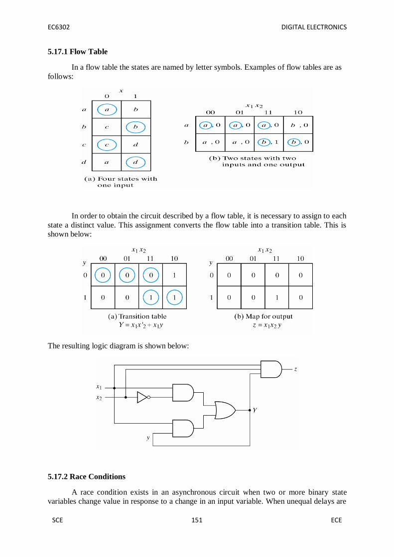
EC6302 DIGITAL ELECTRONICS
SCE 151 ECE
5.17.1 Flow Table
In a flow table the states are named by letter symbols. Examples of flow tables are as
follows:
In order to obtain the circuit described by a flow table, it is necessary to assign to each
state a distinct value. This assignment converts the flow table into a transition table. This is
shown below:
The resulting logic diagram is shown below:
5.17.2 Race Conditions
A race condition exists in an asynchronous circuit when two or more binary state
variables change value in response to a change in an input variable. When unequal delays are

EC6302 DIGITAL ELECTRONICS
SCE 152 ECE
encountered, a race condition may cause the state variable to change in an unpredictable
manner.
If the final stable state that the circuit reaches does not depend on the order in which
the state variables change, the race is called a non critical race. Examples of non critical
races are illustrated in the transition tables below:
The transition tables below illustrate critical races:
Races can be avoided by directing the circuit through a unique sequence of
intermediate unstable states. When a circuit does that, it is said to have a cycle.
Examples of cycles are:

EC6302 DIGITAL ELECTRONICS
SCE 153 ECE
5.17.3 ANALYSIS EXAMPLE
Consider the following circuit:
The first step is to obtain the Boolean functions for the S and R inputs in each latch:
S1 = X1y2 S2 = X1 X2 R1 = X1’X2’ R2 = X2’y1
The next step is to check if SR = 0 is satisfied:
The next step is to derive the transition table of the circuit. The excitation functions
are derived from the relation Y = S + R′y as:
Next a composite map for Y = Y1Y2 is developed:

EC6302 DIGITAL ELECTRONICS
SCE 154 ECE
Investigation of the transition table reveals that the circuit is stable. There is a critical race
condition when the circuit is initially in total state y1y2x1x2 = 1101 and x2 changes from 1 to
0. If Y1 changes to 0 before Y2, the circuit goes to total state 0100 instead of 0000.
5.17.4 DESIGN PROCEDURE
There are a number of steps that must be carried out in order to minimize the circuit
complexity and to produce a stable circuit without critical races. Briefly, the design steps are
as follows:
1. Obtain a primitive flow table from the given specification.
2. Reduce the flow table by merging rows in the primitive flow table.
3. Assign binary states variables to each row of the reduced flow table to
obtain the transition table.
4. Assign output values to the dashes associated with the unstable states to
obtain the output maps.
5. Simplify the Boolean functions of the excitation and output variables and
draw the logic diagram.
The design process will be demonstrated by going through a specific example:
5.17.5 Design Example – Specification
Design a gated latch circuit with two inputs, G (gate) and D (data), and one output Q.
The gated latch is a memory element that accepts the value of D when G = 1 and retains this
value after G goes to 0. Once G = 0, a change in D does not change the value of the output Q.
Step 1: Primitive Flow Table
A primitive flow table is a flow table with only one stable total state in each row. The
total state consists of the internal state combined with the input.
To derive the primitive flow table, first a table with all possible total states in the
system is needed:
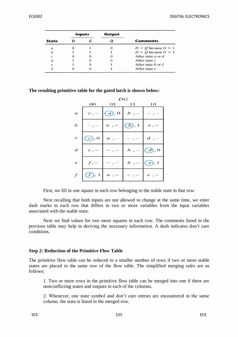
EC6302 DIGITAL ELECTRONICS
SCE 155 ECE
The resulting primitive table for the gated latch is shown below:
First, we fill in one square in each row belonging to the stable state in that row.
Next recalling that both inputs are not allowed to change at the same time, we enter
dash marks in each row that differs in two or more variables from the input variables
associated with the stable state.
Next we find values for two more squares in each row. The comments listed in the
previous table may help in deriving the necessary information. A dash indicates don’t care
conditions.
Step 2: Reduction of the Primitive Flow Table
The primitive flow table can be reduced to a smaller number of rows if two or more stable
states are placed in the same row of the flow table. The simplified merging rules are as
follows:
1. Two or more rows in the primitive flow table can be merged into one if there are
nonconflicting states and outputs in each of the columns.
2. Whenever, one state symbol and don’t care entries are encountered in the same
column, the state is listed in the merged row.

EC6302 DIGITAL ELECTRONICS
SCE 156 ECE
3. If the state is circled in one of the rows, it is also circled in the merged row.
4. The output state is included with each stable state in the merged row.
Now apply these rules to the primitive flow table shown previously.
To see how this is done the primitive flow table is separated into two parts of three rows
each:
Each part shows three stable states that can be merged because there no conflicting
entries in each of the four columns. Since a dash represents a don’t care condition it can be
associated with any state or output. The first column of can be merged into a stable state c
with output 0, the second into a stable state a with output 0, etc.
The resulting reduced flow table is as follows:
Step 3: Transition Table and Logic Diagram
To obtain the circuit described by the reduced flow table, a binary value must be
assigned to each state. This converts the flow table to a transition table.
In assigning binary states, care must be taken to ensure that the circuit will be free of
critical races. No critical races can occur in a two-row flow table.
Assigning 0 to state a and 1 to state b in the reduced flow table, the following
transition table is obtained:

EC6302 DIGITAL ELECTRONICS
SCE 157 ECE
The transition table is, in effect, a map for the excitation variable Y. The simplified
Boolean function for Y as obtained from the map is:
Y = DG +G′’y
There are two don’t care outputs in the final reduced flow table. By assigning values
to the output as shown below:
It is possible to make output Q equal to Y. If the other possible values are assigned to
the don’t care outputs, output Q is made equal to y. In either case, the logic diagram of the
gated latch is as follows:
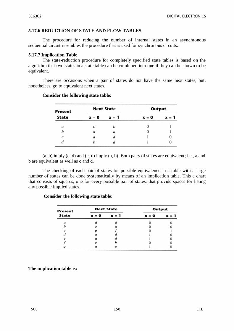
EC6302 DIGITAL ELECTRONICS
SCE 158 ECE
5.17.6 REDUCTION OF STATE AND FLOW TABLES
The procedure for reducing the number of internal states in an asynchronous
sequential circuit resembles the procedure that is used for synchronous circuits.
5.17.7 Implication Table
The state-reduction procedure for completely specified state tables is based on the
algorithm that two states in a state table can be combined into one if they can be shown to be
equivalent.
There are occasions when a pair of states do not have the same next states, but,
nonetheless, go to equivalent next states.
Consider the following state table:
(a, b) imply (c, d) and (c, d) imply (a, b). Both pairs of states are equivalent; i.e., a and
b are equivalent as well as c and d.
The checking of each pair of states for possible equivalence in a table with a large
number of states can be done systematically by means of an implication table. This a chart
that consists of squares, one for every possible pair of states, that provide spaces for listing
any possible implied states.
Consider the following state table:
The implication table is:
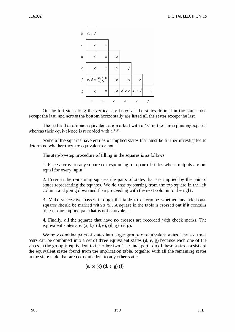
EC6302 DIGITAL ELECTRONICS
SCE 159 ECE
On the left side along the vertical are listed all the states defined in the state table
except the last, and across the bottom horizontally are listed all the states except the last.
The states that are not equivalent are marked with a ‘x’ in the corresponding square,
whereas their equivalence is recorded with a ‘√’.
Some of the squares have entries of implied states that must be further investigated to
determine whether they are equivalent or not.
The step-by-step procedure of filling in the squares is as follows:
1. Place a cross in any square corresponding to a pair of states whose outputs are not
equal for every input.
2. Enter in the remaining squares the pairs of states that are implied by the pair of
states representing the squares. We do that by starting from the top square in the left
column and going down and then proceeding with the next column to the right.
3. Make successive passes through the table to determine whether any additional
squares should be marked with a ‘x’. A square in the table is crossed out if it contains
at least one implied pair that is not equivalent.
4. Finally, all the squares that have no crosses are recorded with check marks. The
equivalent states are: (a, b), (d, e), (d, g), (e, g).
We now combine pairs of states into larger groups of equivalent states. The last three
pairs can be combined into a set of three equivalent states (d, e, g) because each one of the
states in the group is equivalent to the other two. The final partition of these states consists of
the equivalent states found from the implication table, together with all the remaining states
in the state table that are not equivalent to any other state:
(a, b) (c) (d, e, g) (f)

EC6302 DIGITAL ELECTRONICS
SCE 160 ECE
The reduced state table is:
5.17.8 Merging of the Flow Table
There are occasions when the state table for a sequential circuit is incompletely
specified.
Incompletely specified states can be combined to reduce the number of states in the
flow table. Such states cannot be called equivalent,
but, instead they are said to be compatible.
The process that must be applied in order to find a suitable group of compatibles for
the purpose of merging a flow table is divided into three steps:
1. Determine all compatible pairs by using the implication table.
2. Find the maximal compatibles using a merger diagram.
3. Find a minimal collection of compatibles that covers all the states and is closed.
We will now proceed to show and explain the three procedural steps using the
following primitive flow table:

EC6302 DIGITAL ELECTRONICS
SCE 161 ECE
5.17.9 Compatible Pairs
Two states are compatible if in every column of the corresponding rows in the flow
table, they are identical or compatible states and if there is no conflict in the output values.
The compatible pairs (√) are:
(a, b) (a, c) (a, d) (b, e) (b, f) (c, d) (e, f)
5.17.10 Maximal Compatibles
The maximal compatible is a group of compatibles that contains all the possible
combinations of compatible states. The maximal compatible can be obtained from a merger
diagram:
The above merger diagram is obtained from the list of compatible pairs derived from
the previous implication table. A line represents a compatible pair. A triangle constitutes a
compatible with three states. The maximal compatibles are:
(a, b) (a, c, d) (b, e, f)
In the case where a state is not compatible to any other state, an isolated dot
represents this state.

EC6302 DIGITAL ELECTRONICS
SCE 162 ECE
5.20. RACE-FREE STATE ASSIGNMENT
The main objective in choosing a proper binary state assignment is the prevention of
critical races.
Critical races are avoided when states between which transitions occur in a flow table
are given adjacent assignments. (e.g., 010 and 111 are adjacent).
No critical races can occur in a two-row flow table.
5.21 Three-Row Flow Table Example
Consider the following reduced flow-table. For simplicity the outputs have been
omitted:
In row a there is a transition from state a to state c and from state a to state c.
This information is transferred into a transition diagram:
The binary state assignment in the transition table will cause a critical race during the
transition from a to c because there are two changes in the binary state variables.
A race-free assignment can be obtained by adding an extra row to the flow table:

EC6302 DIGITAL ELECTRONICS
SCE 163 ECE
The use of a fourth row does not increase the number of binary state variables, but
allows the formation of cycles between two stable states.
The two dashes represent unspecified states and can be considered don’t care
conditions. However, 10 must not be assigned to these squares to avoid an unwanted stable
state in the fourth row.
5.22 Four-Row Flow Table Example
A flow table with four rows requires a minimum of two state variables.
Consider the following flow table and its corresponding transition diagram:
A state assignment map that is suitable for any four-row flow table is shown
below:

EC6302 DIGITAL ELECTRONICS
SCE 164 ECE
States a, b, c, and d are the original states, and e, f, and g are extra states. The
assignment ensures that a cycle is produced so that only one binary variable changes at a
time.
By using the assignment given by the map, the four-row table can be expanded to
a seven-row table that is free of critical races:
5.23HAZARDS
Hazards are unwanted switching transients that may appear at the output of a circuit
because different paths exhibit different propagation delays.
Hazards occur in combinational circuits, where they may cause a temporary false-
output value. When this condition occurs in asynchronous sequential circuits, it may result in
a transition to a wrong stable state.

EC6302 DIGITAL ELECTRONICS
SCE 165 ECE
5.24 Hazards in Combinational Circuits
The following circuit demonstrates the occurrence of a hazard:
Assume that all three inputs are initially equal to 1. Then consider a change of x2
from 1 to 0. The output momentarily may go to 0 if the propagation through the inverter is
taken into account.
The circuit implements the Boolean function in sum-of-products
Y = x1x2 + x2’ x3
This type of implementation may cause the output to go to 0 when it should remain a
1. This is known as a static 1-hazard:
If the circuit was implemented in product-of-sums, namely:
Y = (x1 + x2’ )(x2 + x3 )
Then the output may momentarily go to 1 when it should remain 0. This is referred to
as a static 0-hazard:
A third type of hazard, known as dynamic hazard causes the output to change 2 or 3
time when it should be change from 1 to 0 or 0 to 1:

EC6302 DIGITAL ELECTRONICS
SCE 166 ECE
The occurrence of the hazard can be detected by inspecting the map of the particular
circuit:
Y = x1x2 + x2’x3
The remedy for eliminating a hazard is to enclose the two minterms in question with
another product term that overlaps both groupings:
Y = x1x2 + x2’x3 + x1x3
The hazard-free circuit is:

EC6302 DIGITAL ELECTRONICS
SCE 167 ECE
5.25 Hazards in Sequential Circuits
Consider the following asynchronous sequential circuit:
If the circuit is in total state yx1x2 = 111 and input x2 changes from 1 to 0, the next
total state should be 110. However, because of the hazard, output Y may go 0 momentarily.
If this false signal feeds back into gate 2 before the output of the inverter goes to 1,
the output of gate 2 will remain at 0 and the circuit will switch to the incorrect total state 010.
This can be eliminated by adding an extra gate.
5.26 Essential Hazards
An essential hazard is the result of the effects of a single input variable change
reaching one feedback path before another feedback path.
Essential hazards cannot be corrected by adding redundant gates as in static hazards.
They can always be eliminated in a realization by the insertion of sufficient delays in
the feedback paths. Facility in doing this comes only with experience.
5.27 ASM CHART
Sooner or later you will discover that state diagrams can become very messy. In many
cases just drawing a state diagram includes certain assumptions that are not true in general.
Perhaps certain cases of inputs will never happen, hence the corresponding arcs are simply
not drawn. Certain cases of outputs are not significant and sometimes are left out. An
algorithmic state machine (ASM) diagram offers several advantages over state diagrams:
For larger state diagrams, often are easier to intpret
conditions for a proper state diagram are automatically satisfied
may be easily coverted to other forms
A key point to remember about ASM charts is that given a state, they do not enumerate all
the possible inputs and outputs. Only the inputs that matter and the outputs that are asserted
are indicated. It must be known whether a signal is positive or negative logic:

EC6302 DIGITAL ELECTRONICS
SCE 168 ECE
Positive logic signals that are high are said to be asserted
Negative logic singals that are low are said to be asserted
In this document, a _n suffix is added to indicate negative logic signals.
5.27.1 The ASM Block Diagram
An ASM chart has an entry point and is constructed with blocks. A block is
constucted with the following type of symbols.
One state box. The state box has a name and lists
outputs that are asserted when the system is in that
state. These outputs are called synchronous or Moore
type outputs.
Optional decision box(es). A decision box may be
conditioned on a signal or a test of some kind.
Optional conditional output box(es). Such an ouput
box indicates outputs that are conditionally asserted.
These outputs are called asynchrous or Mealy outputs.
There is no rule saying that outputs are exclusively inside an a conditional output box
or in a state box. An output written inside a state box is simply independent of the input,
while in that state.
The idea is that flow passes from ASM block to ASM block, the decisision boxes
decide the next state and conditional output. Consider the following example of an ASM
diagram block. When state S0 is entered, output Z5 is always asserted. Z1_n however is
asserted only if X2 is also high. Otherwise Z2 is asserted.
An ASM block
5.27.2 Certain Rules
The drawing of ASM charts must follow certain necessary rules:
The entrance paths to an ASM block lead to only one state box Of 'N' possible exit
paths, for each possible valid input combination, only one exit path can be followed, that is
there is only one valid next state.
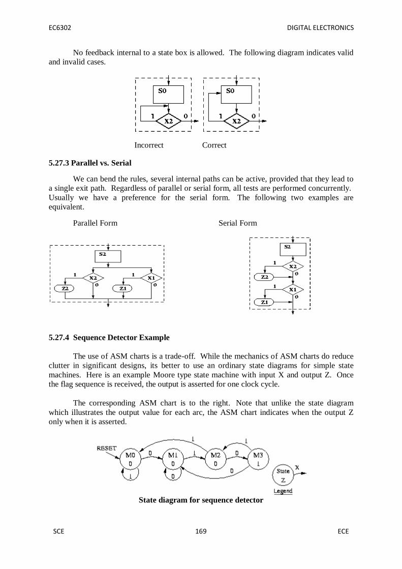
EC6302 DIGITAL ELECTRONICS
SCE 169 ECE
No feedback internal to a state box is allowed. The following diagram indicates valid
and invalid cases.
Incorrect Correct
5.27.3 Parallel vs. Serial
We can bend the rules, several internal paths can be active, provided that they lead to
a single exit path. Regardless of parallel or serial form, all tests are performed concurrently.
Usually we have a preference for the serial form. The following two examples are
equivalent.
Parallel Form Serial Form
5.27.4 Sequence Detector Example
The use of ASM charts is a trade-off. While the mechanics of ASM charts do reduce
clutter in significant designs, its better to use an ordinary state diagrams for simple state
machines. Here is an example Moore type state machine with input X and output Z. Once
the flag sequence is received, the output is asserted for one clock cycle.
The corresponding ASM chart is to the right. Note that unlike the state diagram
which illustrates the output value for each arc, the ASM chart indicates when the output Z
only when it is asserted.
State diagram for sequence detector

EC6302 DIGITAL ELECTRONICS
SCE 170 ECE
The following timing diagram illustrates the detection of the desired sequence. Here
it is assumed that the state is updated with a rising clock edge. The key concept to observe is
that regardless of the input, the output can only be asserted for one entire clock cycle.
Timing diagram
5.27.5 Event Tables
Simply stated, timing diagrams are prone to a particular problem for the reader, in that
there can be too much to see. Timing diagrams clearly expresses time relationships and
delay. However, in synchonous sequential logic, all registers are updated at the rising edge of
the system clock. The clock period is just set to an arbitrarily value. Provided that the input
setup-and-hold requirements are satisfied, the details of the timing diagram are distracting.
The goal of an event table is that given a scenario, to neatly summarize the resultant
behavior of synchronous sequential logic. In writing an event table, capitol T refers to the
system clock period and nT means n times the system clock period. For asynchronous input
changes, the time is given, assuming that the system output reacts instantaneously. For
synchronous signals, the + symbol means a moment suitably after the given time, for the
system to become settled. The - symbol however, means a moment suitably before the given
time, satisfying the necessary setup time.
To reduce the clutter, be sure to fill in those signals that change state or are updated.
The following event table summarizes the behavior in the above timing diagram. An empty
entry will be interpreted to mean no-change to the corresponding signal during the
corresponding clock cycle.
Event Table
Time Reset X State Z
0T 1 0 M0 0
0.4T 0
1T+ M1
1.3T 1
2T+ M2
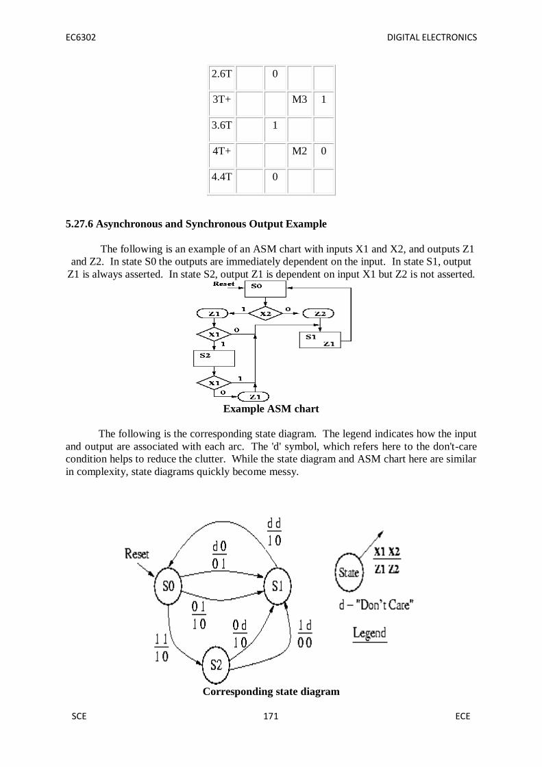
EC6302 DIGITAL ELECTRONICS
SCE 171 ECE
2.6T 0
3T+ M3 1
3.6T 1
4T+ M2 0
4.4T 0
5.27.6 Asynchronous and Synchronous Output Example
The following is an example of an ASM chart with inputs X1 and X2, and outputs Z1
and Z2. In state S0 the outputs are immediately dependent on the input. In state S1, output
Z1 is always asserted. In state S2, output Z1 is dependent on input X1 but Z2 is not asserted.
Example ASM chart
The following is the corresponding state diagram. The legend indicates how the input
and output are associated with each arc. The 'd' symbol, which refers here to the don't-care
condition helps to reduce the clutter. While the state diagram and ASM chart here are similar
in complexity, state diagrams quickly become messy.
Corresponding state diagram

EC6302 DIGITAL ELECTRONICS
SCE 172 ECE
5.27.7 Clock Enable
Simply stated, a clock enable indicates when a state machine must pay attention to the
system clock. The figure below has a clock signal and a clock enable, note that this clock
enable is asserted for one clock period at a time. The clock enable concept is powerful as it
allows a device to effectively be clocked at a rate slower than the system clock, while
remaining entirely synchronous with the rest of the system. In this case the effective clock
rate is one-third that of the system clock.
Clock and enable
In the spirit of reducing clutter, a clock enable can be written next to a state box.
When not asserted, the device remains in its current state. The following figues are
equivalent. Further, it is assumed that devices controlled by such a state, as directly or
indirectly enabled by the clock enable as well.
Equivalent enables.

EC6302 DIGITAL ELECTRONICS
SCE 173 ECE
UNIT 1-MINIMIZATION TECHNIQUES AND LOGIC GATES
PART-A
1. State Demorgan’s Theorem.[April/May-2010,2011,May/June-2013, Nov/Dec-
2010]
De Morgan suggested two theorems that form important part of Boolean algebra.
They are,
1) The complement of a product is equal to the sum of the complements.
(AB)' = A' + B'
2) The complement of a sum term is equal to the product of the complements.
(A + B)' = A'B'
2. Draw an active-high tri-state buffer and write its truth table. [April/May-2010]
Enable Input Output
0 X Z
1 0 0
1 1 1
3. What is a totem pole output? [April/May-2011]
Totem pole output is a standard output of a TTL gate. It is specifically designed to
reduce the propagation delay in the circuit and to provide sufficient output power for
high fan-out.

EC6302 DIGITAL ELECTRONICS
SCE 174 ECE
4. Draw the TTL Inverter (NOT) Circuit. [April/May-2012]
5. Implement using NAND gates only, F=xyz+x′y′.[April/May-2012]
6. What are Don’t care terms? [May/June-2013]
In some logic circuits certain input conditions never occur, therefore the
corresponding output never appears. In such cases the output level is not defined, it
can be either high or low. These output levels are indicated by ‘X’ or ‘d’ in the truth
tables and are called don’t care conditions or incompletely specified functions.
7. Apply De-Morgan’s theorem to [(A+B)+C] ′.[May/June-2014]
Given [(A+B)+C] ′= (A+B) ′.C′
= (A′.B′).C′
[(A+B)+C] ′ = A′B′C′
8. Convert 0.35 to equivalent hexadecimal number. [May/June-2014]
Given (0.35)10 =0.35 x 16=5.60
=0.60 x 16=9.60
=0.60 x 16=9.60
(0.35)10 =(0.599)16
9. Convert Y=A+BC′+AB+A′BC into canonical form. [April/May-2015]
Given Y=A+BC′+AB+A′BC
Y=A(B+B′)(C+C′)+(A+A′)BC′+AB(C+C′)+A′BC
Y=ABC+ABC′+AB′C+AB′C′+ABC′+A′BC′+ABC+ABC′+A′BC
Y=ABC+ABC′+AB′C+AB′C′+A′BC′+A′BC

EC6302 DIGITAL ELECTRONICS
SCE 175 ECE
10. State the advantages of CMOS logic. [April/May-2015]
Consumes less power.
Can be operated at high voltages, resulting in improved noise immunity.
Fan-out is more.
Better noise margin.
11. Define ‘min term’ and ‘max term’. [April/May-2015]
(i) A product term containing all the variables of the function in either
complemented or uncomplemented form is called a min term.
(ii) A sum term containing all the variables of the function in either complemented
or uncomplemented form is called a max term.
12. Write a note on tri-state gates. [April/May-2015]
It is a digital circuit that exhibits three states. Two of the states are signals equivalent
to logic1 and logic 0. The third state is high impedance state. High impedance state
behaves like a open circuit.
13. Prove that the logical sum of all min terms of a Boolean function of 2 variables is
1. [Nov/Dec-2009]
Consider two variables as A and B. For two variables A and B minterms are:
A′B′,A′B,AB′,AB. The logical sum of these minterms are given by
F= A′B′+A′B+AB′+AB
= A′(B′+B)+A(B′+B) (B′+B=1)
= A′(1)+A(1) (A′+A=1)
F=1
Hence it is to be proved.
14. Show that a positive logic NAND gate is a negative logic NOR gate. [Nov/Dec-
2009]

EC6302 DIGITAL ELECTRONICS
SCE 176 ECE
Truth table for positive logic NAND gate and negative logic NOR gates are same and
hence a positive logic NAND gate is negative logic NOR gate.
15. What is the significance of high impedance state in tri-state gates? [Nov/Dec-
2010]
High impedance state of a three-state gate provides a special feature not available in
other gates.
Because of this features a larger number of three state gate output can be connected
with wires to form a common line without endangering loading effects.
16. Simplify the following Boolean Expression to a minimum number of literals.
(BC′+A′D)(AB′+CD′)[Nov/Dec-2011] F=(BC′+A′D)(AB′+CD′)
=BC′AB′+BC′CD′+A′DAB′+A′DCD′ (A.A′=0)
= AB B′C′+BCC′D′+AA′ B′D+A′CDD′
F=0
17. Define the term Fan out. [Nov/Dec-2011]
It is the maximum number of inputs which have same family that the gate can drive
maintaining its output within the specified limits.
18. Simplify the given Boolean Expression F=x′+xy+xz′+xy′z′.[Nov/Dec-2012]
F=x′+xy+xz′+xy′z′
= x′+x(y+z′+y′z′) (A+A′B=A+B)
= x′+y+z′+y′z′
= x′+y+z′(1+y′) (1+A′=1)
F = x′+y+z′
19. Implement the given function using NAND gates F(x,y,z)= Σm(0,6). [Nov/Dec-
2012]
F(x,y,z)=x′y′z′+xyz′
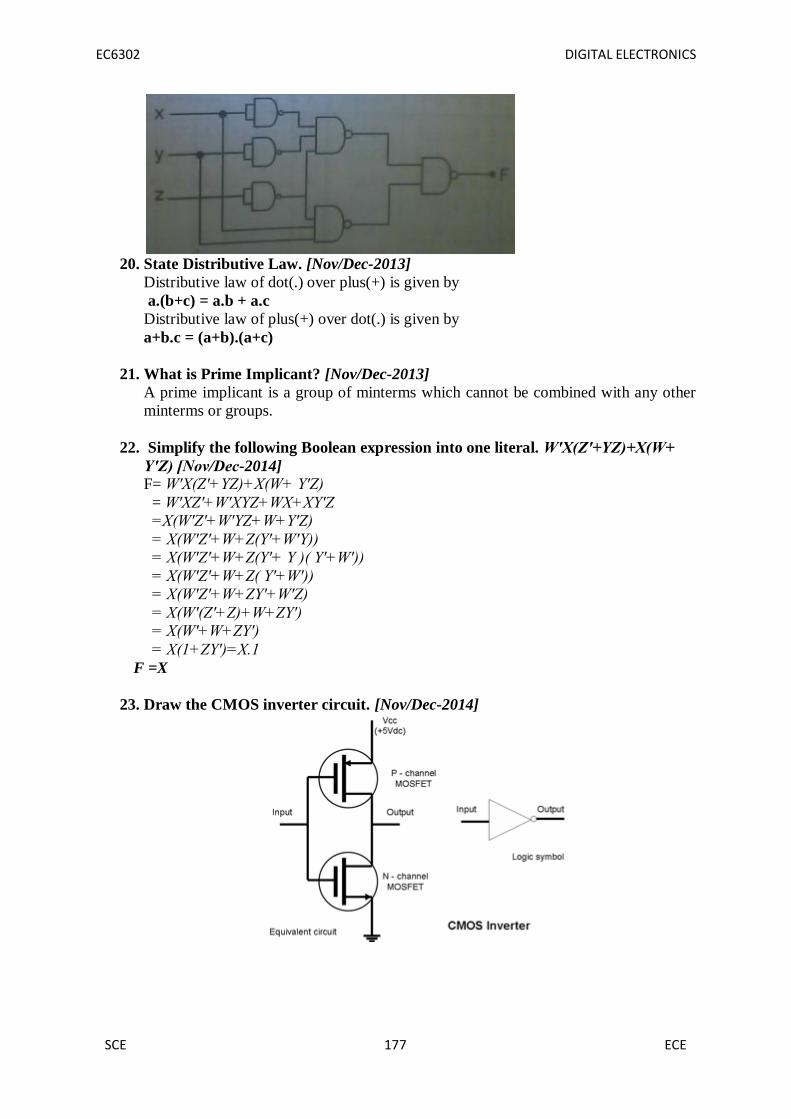
EC6302 DIGITAL ELECTRONICS
SCE 177 ECE
20. State Distributive Law. [Nov/Dec-2013]
Distributive law of dot(.) over plus(+) is given by
a.(b+c) = a.b + a.c
Distributive law of plus(+) over dot(.) is given by
a+b.c = (a+b).(a+c)
21. What is Prime Implicant? [Nov/Dec-2013]
A prime implicant is a group of minterms which cannot be combined with any other
minterms or groups.
22. Simplify the following Boolean expression into one literal. W′X(Z′+YZ)+X(W+
Y′Z) [Nov/Dec-2014]
F= W′X(Z′+YZ)+X(W+ Y′Z)
= W′XZ′+W′XYZ+WX+XY′Z
=X(W′Z′+W′YZ+W+Y′Z)
= X(W′Z′+W+Z(Y′+W′Y))
= X(W′Z′+W+Z(Y′+ Y )( Y′+W′))
= X(W′Z′+W+Z( Y′+W′))
= X(W′Z′+W+ZY′+W′Z)
= X(W′(Z′+Z)+W+ZY′)
= X(W′+W+ZY′)
= X(1+ZY′)=X.1
F =X
23. Draw the CMOS inverter circuit. [Nov/Dec-2014]

EC6302 DIGITAL ELECTRONICS
SCE 178 ECE
UNIT 2- COMBINATIONAL CIRCUITS
PART-A
1 Write an expression for borrow and difference in a full subtractor circuit.
[April/May-2010]
Difference=A′B+AB′=A⊕B
Borrow=A′B
2 Draw the circuits diagram for 4-bit odd parity generator.[April/May-2010]
3 Design a single bit magnitude comparator to compare two words A and B.
[April/May-2011]
4 What is an encoder?[May/June-2012]
An encoder has 2n input lines and n output lines. In encoder the output lines generate the
binary code corresponding to the input value.
5 List few applications of multiplexer.[May/June-2012, Nov/Dec-2013]
Data Selector.
Implement combinational logic circuit.
Time multiplexing systems
Frequency multiplexing systems.
D/A and A/D converter
Data acquisition systems.

EC6302 DIGITAL ELECTRONICS
SCE 179 ECE
6 Design a half subtractor using basic gates.[May/June-2013, Nov/Dec-2010]
Difference=A′B+AB′=A⊕B
Borrow=A′B
7 Draw the logic diagram of a 4 line to 1 line multiplexer. [May/June-2013]
8 What is priority Encoder?[May/June-2014]
A priority encoder is an encoder circuit that includes the priority function. In priority
encoder, if 2 or more inputs are equal to 1 at the same time, the input having the
highest priority will take precedence.

EC6302 DIGITAL ELECTRONICS
SCE 180 ECE
9 Write down the difference between demultiplexer and decoder.[April/May-2015]
Demultiplexer Decoder
Definition 1 data input
2^n outputs
It has n inputs
2^n outputs
It has n control inputs
Characteristic Connects the data input to
the data output
Selects one of the 2^n outputs by
decoding the binary value on the basis of
n inputs
Reverse of Multiplexer Encoder
10 Give the logic expression for sum and carry in full adder circuit.[April/May-
2015]
Sum= (A⊕B)⊕Cin
Carry=AB+BCin+A Cin
11 Give examples for combinational circuit.[April/May-2015, Nov/Dec-2013]
i. Adders
ii. Subtractors
iii. Multiplexers
iv. Demultiplexers
v. Encoders
vi. Decoders
12 Draw the logic circuit of a 2-bit comparator.[April/May-2015,2014]

EC6302 DIGITAL ELECTRONICS
SCE 181 ECE
13 Suggest a solution to overcome the limitation on the speed of an adder.[Nov/Dec-
2009]
It is possible to increase speed of adder by eliminating inter-stage carry delay. This
method utilizes logic gates to look at the lower-order bits of the augend and addend to
see if a higher-order carry is to be generated.
14 Relate carry generate, Carry propagate, Sum and Carry-out of a Carry look a
head adder.[Nov/Dec-2010]
15 Realize the Boolean function using appropriate multiplexer F(A,B,C)= Σ (0,1,3,7)
[Nov/Dec-2010]
16 Compare the performance of binary serial and parallel adders.[Nov/Dec-2011]
Serial Adder:
Serial adder uses shift registers
The serial adder requires only one full adder circuit
The serial adder is a sequential circuit
Time required for addition depends on the number of bits
It is slower
parallel adder:
Parallel adder uses registers with parallel load capacity
It is faster
Time required for addition does not depend on number of bits
Excluding the registers, the parallel adder is a purely combinational circuit

EC6302 DIGITAL ELECTRONICS
SCE 182 ECE
17 Design of three bit parity generator.[Nov/Dec-2012]
Odd parity generator:
Even Parity generator:
18 Draw the logic diagram of serial adder.[Nov/Dec-2012]

EC6302 DIGITAL ELECTRONICS
SCE 183 ECE
19 Construct a two-4-bit parallel adder/subtractor using Full Adders and XOR
gates. [Nov/Dec-2014]
20 Convert a two-to-four line decoder with enable input to 1X4 Demultiplexer.
[Nov/Dec-2014]

EC6302 DIGITAL ELECTRONICS
SCE 184 ECE
UNIT 3- SEQUENTIAL CIRCUITS
PART-A
1. Mention any two differences between the edge triggering and level triggering.
[April/May-2010]
Level Triggering:
1) The input signal is sampled when the clock signal is either HIGH or LOW.
2) It is sensitive to Glitches.
Example: Latch.
Edge Triggering:
1) The input signal is sampled at the RISING EDGE or FALLING EDGE of the clock
signal.
2) It is not-sensitive to Glitches.
Example: Flipflop.
2. What is meant by programmable counter? Mention its application. [April/May-
2010]
A counter that divides an input frequency by a number which can be programmed
into decades of synchronous down counters.
Decades, with additional decoding and control logic, give the equivalent of a divide-
by N counter system, where N can be made equal to any number.
Appication:
Microprocessor.
Traffic light controller.
Street light controller.
3. Write the characteristic equation of a JK flip-flop. [April/May-2011, Nov/Dec-
2009]
The characteristic equation of a JK flip-flop is given by
Q(next) = JQ' + K'Q
4. State the differences between Moore and mealy state machine. [April/May-
2011,Nov/Dec-2010,2011]
1)Mealy Machines tend to have less states
a) Different outputs on arcs (n^2) rather than states (n).
2) Moore Machines are safer to use
a) Outputs change at clock edge (always one cycle later).
b) In Mealy machines, input change can cause output change as soon as logic is done
– a big problem when two machines are interconnected asynchronous feedback.
3) Mealy Machines react faster to inputs
b) React in same cycle – don't need to wait for clock.
c) In Moore machines, more logic may be necessary to decode state into outputs –
more gate delays after.

EC6302 DIGITAL ELECTRONICS
SCE 185 ECE
5. Realise T-FF from JK-FF. [April/May-2012]
6. Convert JK flip-flop to T flip-flop. [April/May-2013, 2012]
7. How many flip-flops are required to build a binary counter that counts from 0 to
1023? [April/May-2013]
If the number of flip-flops required is n, then
2n-1=1023 n=10 since 2
10=1024
8. Compare the logics of synchronous counter and ripple counter. [April/May-2014,
Nov/Dec-2009]
Asynchronous counter:
1. In this type of counter flipflop are connected in such a way that output of first
flip-flop drives the clock for next flip-flop.
2. All the flip-flop are not clocked simultaneously.
3. Logic circuit is very simple even for more number of states.
synchronous counter:
1. In this type there is no connection between output of first flip-flop and clock
input of the next flip-flop.
2. All the flip-flop are clocked simultaneously.
3. Design involves complex logic circuit as number of states increases.
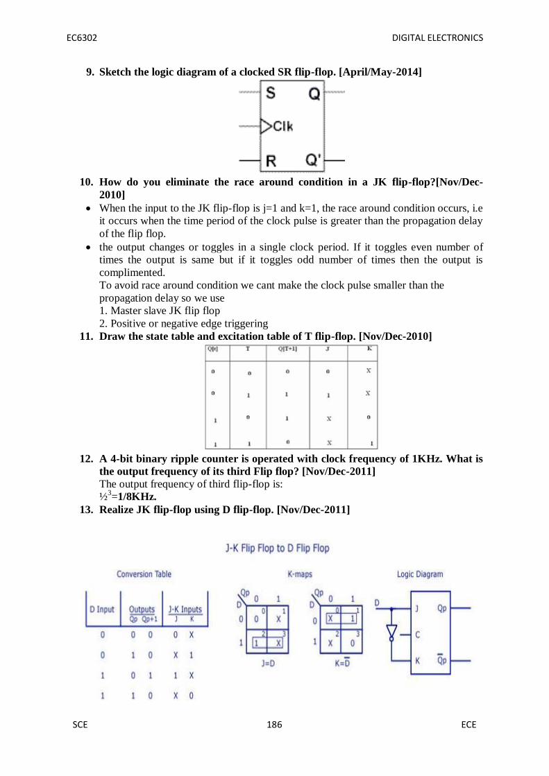
EC6302 DIGITAL ELECTRONICS
SCE 186 ECE
9. Sketch the logic diagram of a clocked SR flip-flop. [April/May-2014]
10. How do you eliminate the race around condition in a JK flip-flop?[Nov/Dec-
2010]
When the input to the JK flip-flop is j=1 and k=1, the race around condition occurs, i.e
it occurs when the time period of the clock pulse is greater than the propagation delay
of the flip flop.
the output changes or toggles in a single clock period. If it toggles even number of
times the output is same but if it toggles odd number of times then the output is
complimented.
To avoid race around condition we cant make the clock pulse smaller than the
propagation delay so we use
1. Master slave JK flip flop
2. Positive or negative edge triggering
11. Draw the state table and excitation table of T flip-flop. [Nov/Dec-2010]
12. A 4-bit binary ripple counter is operated with clock frequency of 1KHz. What is
the output frequency of its third Flip flop? [Nov/Dec-2011]
The output frequency of third flip-flop is:
½3=1/8KHz.
13. Realize JK flip-flop using D flip-flop. [Nov/Dec-2011]

EC6302 DIGITAL ELECTRONICS
SCE 187 ECE
14. Design a 3-bit ring counter and find the mod of the designed counter. [Nov/Dec-
2012]
15. Define latches. [Nov/Dec-2013]
Latch is a simple memory element, which consists of a pair of logic gates with their
inputs and outputs inter connected in a feedback arrangement, which permits a single
bit to be stored.
16. Write short notes on Digital Clock. [Nov/Dec-2013]
A digital clock is a simplified logic diagram of a digital clock that displays seconds,
minutes, and hours. First, a 60 Hz sinusoidal ac voltage is converted to a 60 Hz pulse
waveform and divided own to a 1Hz pulse waveform by a divide-by-60 counter
formed by a divide-by-10 counter allowed by a divide-by-6 counter. Both the seconds
and minutes counts are also produced by divide-by-60 counters.

EC6302 DIGITAL ELECTRONICS
SCE 188 ECE
UNIT 4 - MEMORY DEVICES
PART-A
1. What is meant by memory Expansion? Mention its limit. [April/May-2010]
The memory expansion can be achieved in two ways: by expanding word size and
expanding memory capacity.
Limitations:
1. Memory capacity upto 16Mbytes.
2. 24 address lines and 16 data lines.
2. What are the advantages of static RAM and Dynamic Ram? [April/May-
2010,Nov/Dec-2009]
Static RAM:
Access time is less.
Fast operation.
Dynamic Ram
It consumes less power.
Cost is low.
3. What is difference between PAL and PLA? [April/May-2011, 2013, Nov/Dec-
2010]
PLA:
Both AND and OR arrays are programmable and Complex
Costlier than PAL
PAL:
AND arrays are programmable OR arrays are fixed
Cheaper and Simpler
4. Implement the exclusive or function using ROM. [April/May-2011]
Can implement multi-input/multi-output logic functions inside of ROM.
Data outputs are the logic functions and the address lines are the logic function
inputs.
We create a ROM Table to store the logic functions.
When an input (or address) is presented, the value stored in the specified memory
location appears at the data outputs.
Each data output represents the correct value for its logic function
5. Compare Dynamic RAM with Static RAM. [April/May-2012]
Static Ram is very costly.
Dynamic Ram is cheaper.
Static Ram contains Transistors.
Dynamic Ram contains Capacitors.
Static Ram is used in L1 and L2 cache.
Dynamic Ram is used in system RAM.

EC6302 DIGITAL ELECTRONICS
SCE 189 ECE
6. Mention few applications of PLA and PAL. [April/May-2012]
Implement combinational circuits
Implement sequential circuits
Code converters
Microprocessor based systems
7. What are the different types of programmable logic devices? [April/May-2013]
PROM
PLA
PAL
GAL
8. Draw the structure of a static RAM cell. [April/May-2014]
9. List the advantages of PLDs. [April/May-2014, Nov/Dec-2010]
low and fixed (two gate) propagation delays (typically down to 5 ns),
simple,
low-cost (free),
design tools.
10. What is PAL? [Nov/Dec-2009]
PAL is programmable array logic, PAL consists of a programmable AND array and a
fixed OR array with output logic.
11. What is access time and cycle time of a memory? [Nov/Dec-2010]
Access time is the maximum specified time within which a valid new data is put on
the data bus after an address is applied.
Cycle time is the minimum time for which an address must be held stable on the
address bus in read cycle.

EC6302 DIGITAL ELECTRONICS
SCE 190 ECE
12. Implement a 2-bit multiplier using ROM. [Nov/Dec-2010]
13. How the memories are classified?
It is classified into two types:
volatile
non-volatile memory
14. Draw the logic diagram of a static RAM cell and Bipolar cell. [Nov/Dec-2012]

EC6302 DIGITAL ELECTRONICS
SCE 191 ECE
15. What is volatile and non-volatile memory? [Nov/Dec-2013]
The memory which cannot hold the data when power is turned off is known as
volatile memory.
The memory which can hold the data when power is turned off is known as non-
volatile memory
16. Give the advantages of RAM. [Nov/Dec-2013]
Read and write the data.
Data is accessed by using address of the memory location.
Higher speed.

EC6302 DIGITAL ELECTRONICS
SCE 192 ECE
UNIT-5 SYNCHRONOUS AND ASYNCHRONOUS SEQUENTIAL CIRCUITS
PART-A
1. Draw the block diagram for Moore model. [April/May-2010, 2012]
2. What are hazard free digital circuits? [April/May-2010]
A circuit which has no hazard like static-0-hazard and static-1-hazard is called hazard
free digital circuit.
3. What are the basic building blocks of a algorithmic state machine chart?
[April/May-2011]
4. What are the two types of asynchronous sequential circuits? [April/May-2011]
Fundamental mode circuit
Pulse mode circuit
5. What is state table? [April/May-2012]
The state table representation of a sequential circuit consists of three sections
labelled present state, next state and output. The present state designates the state of
flip-flops before the occurrence of a clock pulse. The next state shows the states of
flip-flops after the clock pulse, and the output section lists the value of the output
variables during the present state.
6. What are Hazards? [April/May-2013, Nov/Dec-2009]
The unwanted switching transients (glitches) that may appear at the output of a circuit
are called Hazards.

EC6302 DIGITAL ELECTRONICS
SCE 193 ECE
7. Distinguish between a flowchart and an ASM chart. [April/May-2013, Nov/Dec-
2009]
A conventional flow chart describes the square of procedural steps and decision
paths for an algorithm without concern for their time relationship.
The ASM chart describes the sequence of event as well as timing relationship
between the states of a sequential controller and the events that occur while going
from one state to the next.
8. What is a state diagram? Give an example. [April/May-2014]
A state diagram is a type of diagram used in computer science and related fields to
describe the behaviour of systems. State diagrams require that the system described is
composed of a finite number of states; sometimes, this is indeed the case, while at
other times this is a reasonable abstraction. Many forms of state diagrams exist, which
differ slightly and have different semantics.
9. Write the VHDL code for a half adder. [April/May-2014]
HALF ADDER –
Entity entity
HALFADD is port ( A,B : in bit; S,C : out bit );
end HALFADD; --
Architecture
Architecture struct of HALFADD is
begin S <= A xor B;
C <= A and B;
end struct;
10. Write a verilog model of a full subtractor circuit. [Nov/Dec-2010]
module full_subtractor ( a ,b ,c ,diff ,borrow );
output diff ;
output borrow ;
input a ;
input b ;
input c ;
assign diff = a ^ b ^ c;
assign borrow = ((~a) & b) | (b & c) | (c & (~a));
endmodule
11. Under what circumstances asynchronous circuits are prepared. [Nov/Dec-2011]
(i) Fundamental mode asynchronous circuits
(ii) Pulse mode asynchronous circuits
12. Differentiate fundamental mode and pulse mode asynchronous sequential
circuits. [Nov/Dec-2012]
Fundamental mode sequential circuits Pulse mode sequential circuits.
(i)Memory elements are clocked flip-flops (i) Memory elements are either unlocked flip -flops or time delay elements.
(ii)Easier to design (ii)More difficult to design

EC6302 DIGITAL ELECTRONICS
SCE 194 ECE
13. Design a 3 input AND gate using verilog. [Nov/Dec-2012]
module and ( a ,b ,c ,f);
output diff ;
input a ;
input b ;
input c ;
assign f = a &b & c;
endmodule
14. What is synchronous sequential circuit? [Nov/Dec-2013]
In synchronous circuits the input are pulses (or levels and pulses) with certain
restrictions on pulse width and circuit propagation delay. Therefore synchronous
circuits can be divided into clockedsequential circuits and uncklocked or
pulsed sequential circuits.
In a clocked sequential circuit which has flip-flops or, in some instances, gated
latches, for its memory elements there is a (synchronizing) periodic clock connected
to the clock inputs of all the memory elements of the circuit, to synchronize all
internal changes of state
15. Write short notes on Hazards. [Nov/Dec-2013]
The unwanted switching transients (glitches) that may appear at the output of a circuit
are called Hazards.
Static-0-Hazard
Static-1-Hazard

EC6302 DIGITAL ELECTRONICS
SCE 195 ECE
QUESTION BANK
UNIT-I
MINIMIZATION TECHNIQUES AND LOGIC GATES
PART-A
1. State Demorgan’s Theorem.[April/May-2010,2011,May/June-2013, Nov/Dec-2010]
2. Draw an active-high tri-state buffer and write its truth table. [April/May-201
3. What is a totem pole output? [April/May-2011]
4. Draw the TTL Inverter (NOT) Circuit. [April/May-2012]
5. Implement using NAND gates only, F=xyz+x′y′.[April/May-2012]
6. What are Don’t care terms? [May/June-2013]
7. Apply De-Morgan’s theorem to [(A+B)+C] ′.[May/June-2014]
8. Convert 0.35 to equivalent hexadecimal number. [May/June-2014]
9. Convert Y=A+BC′+AB+A′BC into canonical form. [April/May-2015]
10. State the advantages of CMOS logic. [April/May-2015]
11. Define ‘min term’ and ‘max term’. [April/May-2015]
12. Write a note on tri-state gates. [April/May-2015]
13. Prove that the logical sum of all min terms of a Boolean function of 2 variables is 1.
[Nov/Dec-2009]
14. Show that a positive logic NAND gate is a negative logic NOR gate. [Nov/Dec-2009]
15. What is the significance of high impedance state in tri-state gates? [Nov/Dec-2010]
16. Simplify the following Boolean Expression to a minimum number of literals.
(BC′+A′D)(AB′+CD′)[Nov/Dec-2011]
17. Define the term Fan out. [Nov/Dec-2011]
18. Simplify the given Boolean Expression F=x′+xy+xz′+xy′z′.[Nov/Dec-2012]
19. Implement the given function using NAND gates F(x,y,z)= Σm(0,6). [Nov/Dec-2012]
20. State Distributive Law. [Nov/Dec-2013]
21. What is Prime Implicant? [Nov/Dec-2013]
22. Simplify the following Boolean expression into one literal. W′X(Z′+YZ)+X(W+ Y′Z)
[Nov/Dec-2014]
23. Draw the CMOS inverter circuit. [Nov/Dec-2014]
PART-B
1. Express the Boolean function as
1) POS form
2) SOP form
D=(A′+B)(B′+C)[April/May-2010] (4)
2. Minimize the given terms πM (0, 1, 4, 11, 13, 15) + πd (5, 7, 8) using Quine-
McClusky methods and verify the results using K-map methods.[April/May-2010]
(12)
3. Implement the following function using NOR gates. [April/May-2010] (8)

EC6302 DIGITAL ELECTRONICS
SCE 196 ECE
Output = 1 when the inputs are Σ m(0,1,2,3,4)
= 0 when the inputs are Σ m(5,6,7) .
4. Discuss the general characteristic of TTL and CMOS logic families. [April/May-
2010] (8)
5. Express the Boolean function F=A+B′C in sum of min terms[April/May-2011] (6)
6. Simplify the Boolean function using K-map. F (w, x , y, z ) = Σ(0, 1, 2, 4, 5, 6, 8, 9,
12, 13, 14 ) [April/May-2011] (10)
7. Draw the schematic and explain the operation of a CMOS inverter. Also explain its
characteristics. [April/May-2011] (8)
8. State and verify DeMorgan’s Law. [April/May-2012] (3)
9. Simplify the Boolean expression
F=x′y′z′+x′yz+xy′z′+xyz′[April/May-2012] (5)
10. Minimize the Function, F using Quine Mcclusky Method.
F= Σ(0,1,2,8,10,11,14,15) [April/May-2012,2013] (8)
11. Differentiate between Min Term and Max Term.[April/May-2012] (4)
12. Using Karnaugh map simplify the following expressions and implement using basic
gates. [April/May-2012] (12)
1) F= Σ(1,3,4,6)
2) F= Σ(1,3,7,11,15)+d(0,2,5)
13. Simplify the Boolean function into[April/May-2013]
(i) Sum of product form. (8)
(ii) Product of sum form. (8)
F(A,B,C,D)= Σ(0,1,2,5,8,9,10)
14. Express the Boolean function F=XY+X′Z in product of Maxterm.[Nov/Dec-2009]
Given (6)
15. Reduce the following function using K-map technique. [Nov/Dec-2009] (10)
F(A,B,C,D)= π(0,3,4,7,8,10,12,14)+d(2,6)
16. Simplify the following Boolean function by using a Quine-McCluskey method.
F (A, B, C, D) = Σm(0, 2, 3, 6, 7, 8, 10, 12, 13 ) [Nov/Dec-2009] (16)
17. Simplify the following Boolean function using 4-variable map
F (w,x,y,z) = Σ( 2, 3, 10,11,12, 13,14,15) [Nov/Dec-2010] (8)
18. Draw a NAND logic diagram that implements the complement of the following
function.
F (A, B, C, D) = Σ(0,1,2, 3,4,8,9,12) [Nov/Dec-2010] (8)
19. Draw and explain Tri-state TTL inverter circuit diagram and explain its operation.
[Nov/Dec-2014] (12)
UNIT-II
COMBINATIONAL CIRCUITS
PART-A
1 Write an expression for borrow and difference in a full subtractor circuit. [April/May-
2010]
2 Draw the circuits diagram for 4-bit odd parity generator.[April/May-2010]
3 Design a single bit magnitude comparator to compare two words A and B.

EC6302 DIGITAL ELECTRONICS
SCE 197 ECE
[April/May-2011]
4 What is an encoder?[May/June-2012]
5 List few applications of multiplexer.[May/June-2012, Nov/Dec-2013]
6 Design a half subtractor using basic gates.[May/June-2013, Nov/Dec-2010]
7 Draw the logic diagram of a 4 line to 1 line multiplexer. [May/June-2013]
8 What is priority Encoder?[May/June-2014]
9 Write down the difference between demultiplexer and decoder.[April/May-2015]
10 Give the logic expression for sum and carry in full adder circuit.[April/May-2015]
11 Give examples for combinational circuit.[April/May-2015, Nov/Dec-2013]
12 Draw the logic circuit of a 2-bit comparator.[April/May-2015,2014]
13 Suggest a solution to overcome the limitation on the speed of an adder.[Nov/Dec-
2009]
14 Relate carry generate, Carry propagate, Sum and Carry-out of a Carry look a head
adder.[Nov/Dec-2010]
15 Realize the Boolean function using appropriate multiplexer F(A,B,C)= Σ (0,1,3,7)
[Nov/Dec-2010]
16 Compare the performance of binary serial and parallel adders.[Nov/Dec-2011]
17 Design of three bit parity generator.[Nov/Dec-2012]
18 Draw the logic diagram of serial adder.[Nov/Dec-2012]
19 Construct a two-4-bit parallel adder/subtractor using Full Adders and XOR gates.
[Nov/Dec-2014]
20 Convert a two-to-four line decoder with enable input to 1X4
Demultiplexer.[Nov/Dec-2014]
PART-B
1. Derive the equation for a 4-bit look ahead carry adder circuit.[April/May-
2010,2014,2015, Nov/Dec-2009,2010]
2. Draw and explain the block diagram of a 4-bit serial adder to add the contents of two
registers. [April/May-2010]
3. Multiply(1011)2 by (1101)2 using addition and shifting operation also draw the block
diagram of the 4-bit by 4-bit parallel multiplier. [April/May-2010]
4. Design and implement the conversion circuits for binary code to gray code.
[April/May-2010,2014,2015]
5. Design a full adder using two half adders and an OR gate. [April/May-2011]
6. Explain the operation of a BCD adder. [April/May-2011,2012,2013,2015, Nov/Dec-
2012]
7. Draw the logic diagram of a 2-bit by 2-bit binary multiplier and explain its operation.
[April/May-2011,Nov/Dec-2010]
8. Implement the following function using suitable multiplexer. [April/May-2011,2015]
F(A,B,C,D)= Σ (1,3,4,11,12,13,14,15)
9. Design a 4-bit word comparator, so that the output follows the table 1. [April/May-
2011,2013,2015, Nov/Dec-2011,2013]
10. Design a 3:8 decoder using basic gates. [April/May-2014, Nov/Dec-2011]
EC6302 DIGITAL ELECTRONICS
SCE 198 ECE
11. Design a full subtractor using demultiplexer. [April/May-2014,Nov/Dec-2009]
12. Implement the given Boolean function using 8:1 multiplexer
F(A,B,C)= Σ (1,3,5,6)
13. Define Fan-in, Fan-out and Noise margin.[Nov/Dec-2010]
14. Design 4:1 Encoder using basic gates.[Nov/Dec-2011]
UNIT-III
SEQUENTIAL CIRCUITS
PART-A
1. Mention any two differences between the edge triggering and level triggering.
[April/May-2010]
2. What is meant by programmable counter? Mention its application. [April/May-2010]
3. Write the characteristic equation of a JK flip-flop. [April/May-2011, Nov/Dec-2009]
4. State the differences between Moore and mealy state machine. [April/May-
2011,Nov/Dec-2010,2011]
5. Realise T-FF from JK-FF. [April/May-2012]
6. Convert JK flip-flop to T flip-flop. [April/May-2013, 2012]
7. How many flip-flops are required to build a binary counter that counts from 0 to
1023? [April/May-2013]
8. Compare the logics of synchronous counter and ripple counter. [April/May-2014,
Nov/Dec-2009]
9. Sketch the logic diagram of a clocked SR flip-flop. [April/May-2014]
10. How do you eliminate the race around condition in a JK flip-flop?[Nov/Dec-2010]
11. Draw the state table and excitation table of T flip-flop. [Nov/Dec-2010]
12. A 4-bit binary ripple counter is operated with clock frequency of 1KHz. What is the
output frequency of its third Flip flop? [Nov/Dec-2011]
13. Realize JK flip-flop using D flip-flop. [Nov/Dec-2011]
14. Design a 3-bit ring counter and find the mod of the designed counter. [Nov/Dec-2012]
15. Define latches. [Nov/Dec-2013]
16. Write short notes on Digital Clock. [Nov/Dec-2013]
PART-B
1. Construct a clocked JK flip-flop which is triggered at the positive edge of the clock
pulse from a clocked SR flip-flop consisting of NOR gates.[April/May-2010,
Nov/Dec-2013]
2. Write down the characteristic table for the JK flip-flop with NOR gates. [April/May-
2010]
3. What is meant by universal counter? Explain the principles of operation of 4-bit
universal shift register. [April/May-2011]
4. Convert D flip-flop to T flip-flop. [April/May-2011]
5. Design serial binary adder. [April/May-2011]
6. Explain the operation of a BCD ripple counter with JK flip-flops. [April/May-
2011,2012,April/May-2013,Nov/Dec-2009]

EC6302 DIGITAL ELECTRONICS
SCE 199 ECE
7. Explain the operation of shift and ring counters. [April/May-2012]
8. Draw the Schematic diagram of up/down counter and explain its operations.
[April/May-2013]
UNIT-IV
MEMORY DEVICES
PART-A
1. What is meant by memory Expansion? Mention its limit. [April/May-2010]
2. What are the advantages of static RAM and Dynamic Ram? [April/May-
2010,Nov/Dec-2009]
3. What is difference between PAL and PLA? [April/May-2011, 2013, Nov/Dec-2010]
4. Implement the exclusive or function using ROM. [April/May-2011]
5. Compare Dynamic RAM with Static RAM. [April/May-2012]
6. Mention few applications of PLA and PAL. [April/May-2012]
7. What are the different types of programmable logic devices? [April/May-2013]
8. Draw the structure of a static RAM cell. [April/May-2014]
9. List the advantages of PLDs. [April/May-2014, Nov/Dec-2010]
10. What is PAL? [Nov/Dec-2009]
11. What is access time and cycle time of a memory? [Nov/Dec-2010]
12. Implement a 2-bit multiplier using ROM. [Nov/Dec-2010]
13. How the memories are classified?
14. Draw the logic diagram of a static RAM cell and Bipolar cell. [Nov/Dec-2012]
15. What is volatile and non-volatile memory? [Nov/Dec-2013]
16. Give the advantages of RAM. [Nov/Dec-2013]
.
PART-B
1. Explain the principle of operation of bipolar SRAM cell. [April/May-2010]
2. Write a note on SRAM based FPGA. [April/May-2010]
3. Design a combinational circuit using a ROM. The circuit accepts a 3-bit number and
generates an output binary number equal to the square of the input number.
[April/May-2011]
4. Briefly explain the EPROM and EEPROM technology. [April/May-2011]
5. With the logic diagram explain the basic macrocell. [April/May-2012]
6. Design 32X8 ROM. [April/May-2013]
7. Discuss the classification of memories. [April/May-,2012,2013,2015]
8. Discuss in detail about the FPGA with suitable diagrams. [April/May-2013,2015]

EC6302 DIGITAL ELECTRONICS
SCE 200 ECE
UNIT-V
SYNCHRONOUS AND ASYNCHRONOUS SEQUENTIAL
CIRCUITS
PART-A
1. Draw the block diagram for Moore model. [April/May-2010, 2012]
2. What are hazard free digital circuits? [April/May-2010]
3. What are the basic building blocks of a algorithmic state machine chart? [April/May-
2011]
4. What are the two types of asynchronous sequential circuits? [April/May-2011]
5. What is state table? [April/May-2012]
6. What are Hazards? [April/May-2013, Nov/Dec-2009]
7. Distinguish between a flowchart and an ASM chart. [April/May-2013, Nov/Dec-
2009]
8. What is a state diagram? Give an example. [April/May-2014]
9. Write the VHDL code for a half adder. [April/May-2014]
10. Write a verilog model of a full subtractor circuit. [Nov/Dec-2010]
11. Under what circumstances asynchronous circuits are prepared. [Nov/Dec-2011]
12. Differentiate fundamental mode and pulse mode asynchronous sequential circuits.
[Nov/Dec-2012]
13. Design a 3 input AND gate using verilog. [Nov/Dec-2012]
14. What is synchronous sequential circuit? [Nov/Dec-2013]
15. Write short notes on Hazards. [Nov/Dec-2013]
PART-B
1. What are called as essential hazards? How does the hazard occur in sequential circuits?
How can the same be eliminated using SR latches? Give an example. [April/May-
2010,2011,2012, Nov/Dec-2012,2013]
2. Write short notes on Hazard free switching circuits. [April/May-2010,2012, 2013]
3. With an example, explain the use of algorithmic state machines. [April/May-
2012,2013]
4. Design a full adder using two half adders by writing Verilog program. [April/May-
2013,2015]
5. Derive the ASM chart for binary multiplier. [April/May-2015]
6. Differentiate critical races from non-critical races. [Nov/Dec-2010]
7. Explain the steps involved in the reduction of state table. [Nov/Dec-2010]
8. Design a JK flip-flop by writing Verilog program. [April/May-2015]
Related Documents


![Three Phase Synchronous Generators - K Power …€¦ · · 2015-11-21Three Phase Synchronous Generators ... Nominal output [kVA] INDUSTRIAL LOW VOLTAGE 0 1000 2000 3000 4000 6](https://static.cupdf.com/doc/110x72/5ac10ee57f8b9ad73f8c7e6a/three-phase-synchronous-generators-k-power-2015-11-21three-phase-synchronous.jpg)