I Code t 9EE'-24 Register Nwnber II Semester Diploma Examination, Nov./Dec., Time Note: : 3 Hours I IMax. Marks : 100 5x1:5 r- I 2. (a) (b) 3. (a) (b) 5 I ELECTRONICS - I Section -l is compulsoryt. (ii) Answer any six fulI questions taking two fulI questions from each section. SECTION _ I 1. (a) Fill in the blanks : (i) If the PN junction is heavily doped, Breakdown voltage will (ii) A semiconductor is temperature co-efficient of resistance. (iii) There are digits in decimal number systems. (iv) In p type semiconductor are the minority carriers. (v) A Boolean expression for two input AND Gate s (b) Explain thermal runway. SECTION _ II Explain the structure of Germanium Silicon. Di fferentiate between intrinsic extrinsic semi conductor. Explain the working PN Junction diode in Forward Bias Reverse Bias with neat diagram. Explain Zener diode as voltage Regulator with neat circuit diagram. 5 Derive the relationship between cr B. 4 [Turn over For More Question Papers Visit - www.pediawikiblog.com For More Question Papers Visit - www.pediawikiblog.com

Welcome message from author
This document is posted to help you gain knowledge. Please leave a comment to let me know what you think about it! Share it to your friends and learn new things together.
Transcript
8/20/2019 2nd SEM Electronics 1 - Dec 2014.pdf
http://slidepdf.com/reader/full/2nd-sem-electronics-1-dec-2014pdf 1/3
I
Code
t
9EE'-24
Register
Nwnber
II Semester
Diploma
Examination,
Nov./Dec.,
Time
Note:
:
3
Hours
I
IMax.
Marks
:
100
5x1:5
2.
(a)
(b)
(c)
3.
(a)
(b)
5
I
ELECTRONICS
-
I
(i)
Section
-l
is
compulsoryt.
(ii)
Answer
any six
fulI
questions taking
two fulI
questions
from
each section.
SECTION
_
I
1.
(a)
Fill
in the blanks
:
(i)
If the PN
junction
is
heavily
doped, Breakdown
voltage
will
(ii)
A
semiconductor
is temperature
co-efficient of
resistance.
(iii)
There
are
digits
in decimal number
systems.
(iv)
In
p
type semiconductor
are
the
minority carriers.
(v)
A Boolean expression
for two input
AND
Gate
is
(b)
Explain thermal runway.
SECTION
_
II
Explain
the structure of Germanium
Silicon.
Di
fferentiate between
intrinsic
extrinsic semi
conductor.
Explain the working
of
PN
Junction
diode
in
Forward
Bias Reverse Bias
with
neat diagram.
Explain
Zener diode
as
voltage Regulator
with neat circuit
diagram.
5
Derive
the relationship between
cr
B.
4
For More Question Papers Visit - www.pediawikiblog.com
8/20/2019 2nd SEM Electronics 1 - Dec 2014.pdf
http://slidepdf.com/reader/full/2nd-sem-electronics-1-dec-2014pdf 2/3
vEE-24
(c)
4.
(a)
7.
(a)
Convert
the
following
:
(i)
(t234.56)rcto
Octal
(ii)
(Vgg.t2)rcto
Hexadecimal
(iii)
(123.236)Bto
Decimal
(b)
Define:
(i)
Bit
(ii)
Nibbte
(iii)
Byte
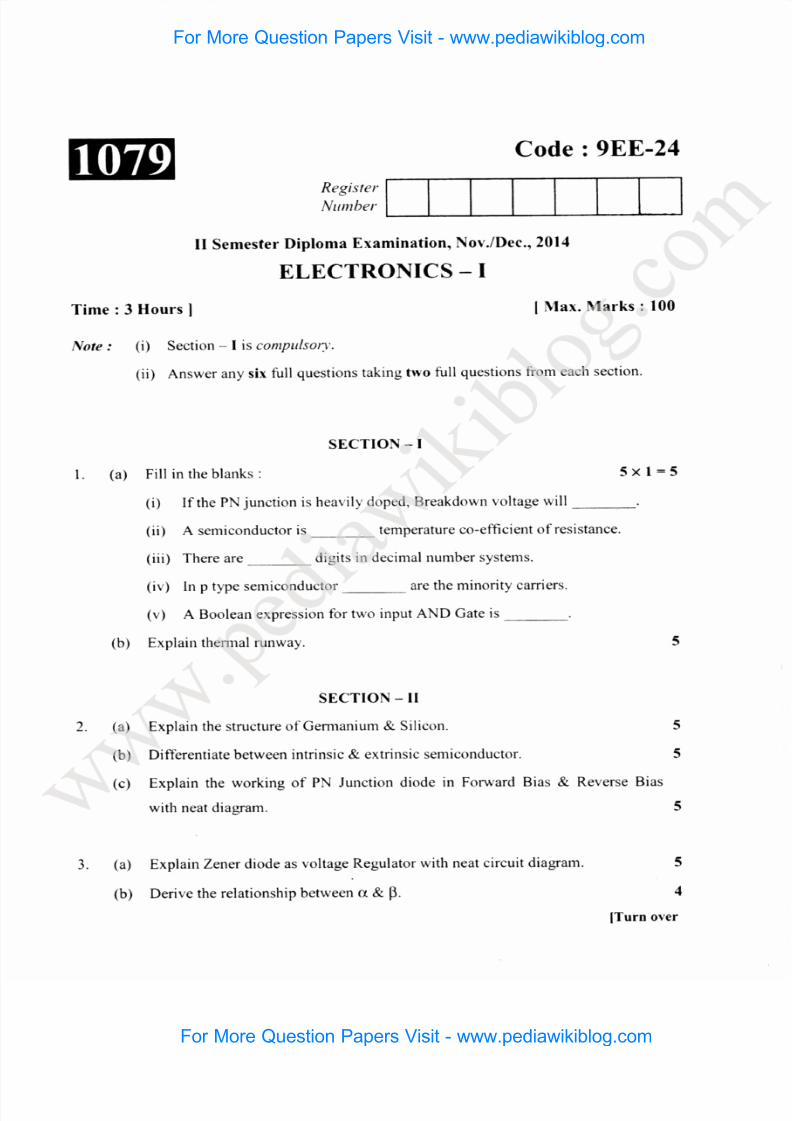
:
't,,,
For
the
circuit,given
below,
Find
(a)
Output
voltage
(b)
Voltage
drop
across
series
resistance
R
(c)
The current
through Zenerdiode
R=2kQ
r
Explain
the
three
regions
of
operation,
saturation,
CE
configuration.
Explain
with
sketch,
the
working
of
MOSFET.
List
the
applications
of
JFET.
R1=
4
kf,)
active
and
cut
offregion
f
(b)
(c)
(a)
(b)
(c)
(a)
(b)
(c)
5.
.
SECTION
_
III
Explain
the
necessity
of
heat
sink
for power
transistor.
Explain
working
of photo
voltaic
cell.
List
any
two applications
each
for LED, LCD
LDR.
Define
SSI,
MSI,
LSI,
VLSI
and
ULSI.
Subtract
(l1000)2
from (1001l),
using
2,s
compliment
method.
Convert
the
following
:
(i)
(35)ro
to
Binary
(ii)
(ABC),6
to Decimal
For More Question Papers Visit - www.pediawikiblog.com
For More Question Papers Visit - www.pediawikiblog.com
8/20/2019 2nd SEM Electronics 1 - Dec 2014.pdf
http://slidepdf.com/reader/full/2nd-sem-electronics-1-dec-2014pdf 3/3
(a)
o)
(c)
3
SECTION
-
IV
Explain
different
laws
in
Boolean
Algebra.
Realize
oR
Gate,
Nor
Gate
Ex-oR
Gate
using
NAND
Gates
only.
Minimize
the following
Boolean
expression
:
Y=(AE(C+B)+As)C
(a)
Draw
Logic
Diagram,
Logic
Symbol,
Expression
and
Truth
Table
for
universal
Gates.
O)
Define
:
(i)
Threshold
voltage
(ii)
Propagation
Delay
(iiD
Noise
Margin
(c)
List
any three
characteristics
of
TTL
family.
(a)
State
Demargon's
Th@re,rns.
p)
Explain
how to
interface
TTL
with LEDS.
(c)
Explain
how to
interface
CMOS
with
motors.
6
6
3
6
6
4
6
5
3
For More Question Papers Visit - www.pediawikiblog.com
For More Question Papers Visit - www.pediawikiblog.com
Related Documents