2018 Microchip Technology Inc. DS20005797A-page 1 2N7002 Features • Free from Secondary Breakdown • Low Power Drive Requirement • Ease of Paralleling • Low C ISS and Fast Switching Speeds • Excellent Thermal Stability • Integral Source-Drain Diode • High Input Impedance and High Gain Applications • Motor Controls • Converters • Amplifiers • Switches • Power Supply Circuits • Drivers (Relays, Hammers, Solenoids, Lamps, Memories, Displays, Bipolar Transistors, etc.) General Description The 2N7002 is a low-threshold, Enhancement-mode (normally-off) transistor that uses a vertical DMOS structure and a well-proven silicon-gate manufacturing process. This combination produces a device with the power handling capabilities of bipolar transistors and the high input impedance and positive temperature coefficient inherent in MOS devices. Characteristic of all MOS structures, this device is free from thermal runaway and thermally induced secondary breakdown. Microchip’s vertical DMOS FETs are ideally suited to a wide range of switching and amplifying applications where very low threshold voltage, high breakdown voltage, high input impedance, low input capacitance and fast switching speeds are desired. Package Type 3-lead SOT-23 (Top view) See Table 3-1 for pin information. DRAIN SOURCE GATE N-Channel Enhancement-Mode Vertical DMOS FET

Welcome message from author
This document is posted to help you gain knowledge. Please leave a comment to let me know what you think about it! Share it to your friends and learn new things together.
Transcript
2N7002N-Channel Enhancement-Mode Vertical DMOS FET
Features
• Free from Secondary Breakdown
• Low Power Drive Requirement
• Ease of Paralleling
• Low CISS and Fast Switching Speeds
• Excellent Thermal Stability
• Integral Source-Drain Diode
• High Input Impedance and High Gain
Applications
• Motor Controls
• Converters
• Amplifiers
• Switches
• Power Supply Circuits
• Drivers (Relays, Hammers, Solenoids, Lamps, Memories, Displays, Bipolar Transistors, etc.)
General Description
The 2N7002 is a low-threshold, Enhancement-mode (normally-off) transistor that uses a vertical DMOS structure and a well-proven silicon-gate manufacturing process. This combination produces a device with the power handling capabilities of bipolar transistors and the high input impedance and positive temperature coefficient inherent in MOS devices. Characteristic of all MOS structures, this device is free from thermal runaway and thermally induced secondary breakdown.
Microchip’s vertical DMOS FETs are ideally suited to a wide range of switching and amplifying applications where very low threshold voltage, high breakdown voltage, high input impedance, low input capacitance and fast switching speeds are desired.
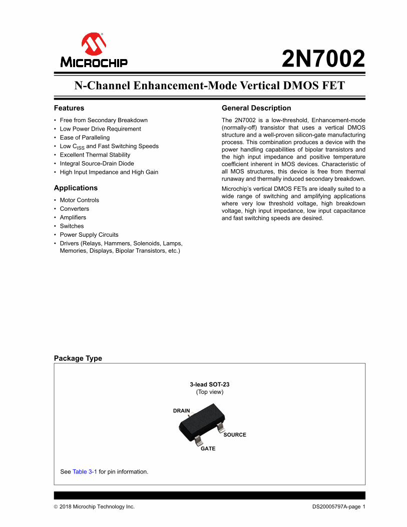
Package Type
3-lead SOT-23(Top view)
See Table 3-1 for pin information.
DRAIN
SOURCE
GATE
2018 Microchip Technology Inc. DS20005797A-page 1
2N7002
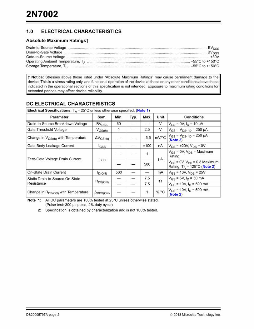
1.0 ELECTRICAL CHARACTERISTICS
Absolute Maximum Ratings†
Drain-to-Source Voltage ...................................................................................................................................... BVDSSDrain-to-Gate Voltage ......................................................................................................................................... BVDGSGate-to-Source Voltage ......................................................................................................................................... ±30VOperating Ambient Temperature, TA ................................................................................................... –55°C to +150°CStorage Temperature, TS ..................................................................................................................... –55°C to +150°C
† Notice: Stresses above those listed under “Absolute Maximum Ratings” may cause permanent damage to the device. This is a stress rating only, and functional operation of the device at those or any other conditions above those indicated in the operational sections of this specification is not intended. Exposure to maximum rating conditions for extended periods may affect device reliability.
DC ELECTRICAL CHARACTERISTICS Electrical Specifications: TA = 25°C unless otherwise specified. (Note 1)
Parameter Sym. Min. Typ. Max. Unit Conditions
Drain-to-Source Breakdown Voltage BVDSS 60 — — V VGS = 0V, ID = 10 µA
Gate Threshold Voltage VGS(th) 1 — 2.5 V VGS = VDS, ID = 250 µA
Change in VGS(th) with Temperature ∆VGS(th) — — –5.5 mV/°CVGS = VDS, ID = 250 µA (Note 2)
Gate Body Leakage Current IGSS — — ±100 nA VGS = ±20V, VDS = 0V
Zero-Gate Voltage Drain Current IDSS
— — 1µA
VGS = 0V, VDS = Maximum Rating
— — 500VGS = 0V, VDS = 0.8 Maximum Rating, TA = 125°C (Note 2)
On-State Drain Current ID(ON) 500 — — mA VGS = 10V, VDS = 25V
Static Drain-to-Source On-State Resistance
RDS(ON)— — 7.5
ΩVGS = 5V, ID = 50 mA
— — 7.5 VGS = 10V, ID = 500 mA
Change in RDS(ON) with Temperature ∆RDS(ON) — — 1 %/°CVGS = 10V, ID = 500 mA (Note 2)
Note 1: All DC parameters are 100% tested at 25°C unless otherwise stated. (Pulse test: 300 µs pulse, 2% duty cycle)
2: Specification is obtained by characterization and is not 100% tested.
DS20005797A-page 2 2018 Microchip Technology Inc.
2N7002
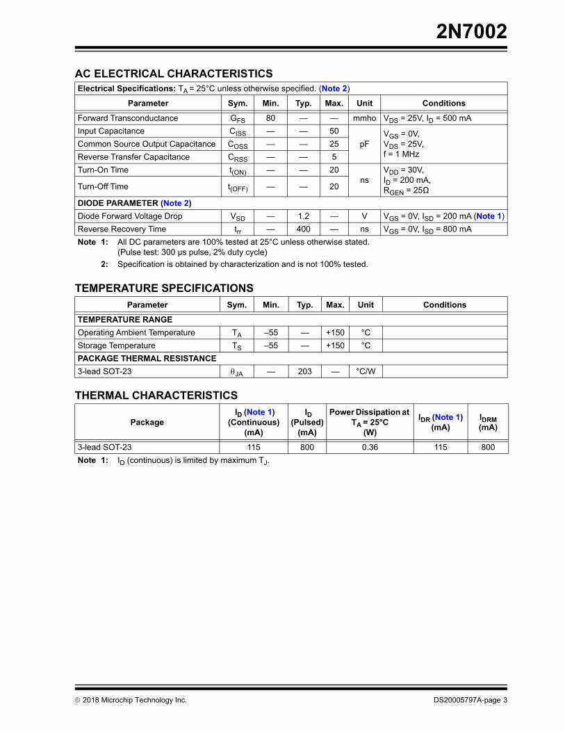
AC ELECTRICAL CHARACTERISTICSElectrical Specifications: TA = 25°C unless otherwise specified. (Note 2)
Parameter Sym. Min. Typ. Max. Unit Conditions
Forward Transconductance GFS 80 — — mmho VDS = 25V, ID = 500 mA
Input Capacitance CISS — — 50
pFVGS = 0V, VDS = 25V, f = 1 MHz
Common Source Output Capacitance COSS — — 25
Reverse Transfer Capacitance CRSS — — 5
Turn-On Time t(ON) — — 20ns
VDD = 30V, ID = 200 mA, RGEN = 25ΩTurn-Off Time t(OFF) — — 20
DIODE PARAMETER (Note 2)
Diode Forward Voltage Drop VSD — 1.2 — V VGS = 0V, ISD = 200 mA (Note 1)
Reverse Recovery Time trr — 400 — ns VGS = 0V, ISD = 800 mA
Note 1: All DC parameters are 100% tested at 25°C unless otherwise stated. (Pulse test: 300 µs pulse, 2% duty cycle)
2: Specification is obtained by characterization and is not 100% tested.
TEMPERATURE SPECIFICATIONS
Parameter Sym. Min. Typ. Max. Unit Conditions
TEMPERATURE RANGE
Operating Ambient Temperature TA –55 — +150 °C
Storage Temperature TS –55 — +150 °C
PACKAGE THERMAL RESISTANCE
3-lead SOT-23 JA — 203 — °C/W
THERMAL CHARACTERISTICS
Package ID (Note 1)
(Continuous)(mA)
ID(Pulsed)
(mA)
Power Dissipation at TA = 25°C
(W)
IDR (Note 1)(mA)
IDRM(mA)
3-lead SOT-23 115 800 0.36 115 800
Note 1: ID (continuous) is limited by maximum TJ.
2018 Microchip Technology Inc. DS20005797A-page 3

2N7002
2.0 TYPICAL PERFORMANCE CURVES
2.0
1.6
1.2
0.8
0.4
00 10 20 30 40 50
4V3V
7V
9V
8V
6V
5V
VGS = 10V
I D (a
mpe
res)
VDS (volts)
Note: The graphs and tables provided following this note are a statistical summary based on a limited number of samples and are provided for informational purposes only. The performance characteristics listed herein are not tested or guaranteed. In some graphs or tables, the data presented may be outside the specified operating range (e.g. outside specified power supply range) and therefore outside the warranted range.
FIGURE 2-1: Output Characteristics. 0.5
0.4
0.3
0.2
0.1
00 0.2 0.4 0.6 0.8 10
TA = -55OC
VDS = 25V
25OC
125OCGFS
(sei
men
s)
ID (amperes)
FIGURE 2-2: Transconductance vs. Drain Current.
0.1 1.0 10 100
1.0
0.1
0.01
0.001
TA = 25OC
SOT-23 (DC)
SOT-23 (pulsed)
VDS (volts)
I D (a
mpe
res)
FIGURE 2-3: Maximum Rated Safe Operating Area.
FIGURE 2-4: Saturation Characteristics.
0 2 4 6 8 10
4V3V
7V
9V
8V
6V
5V
VDS (volts)
I D (a
mpe
res)
VGS = 10V
2.0
1.6
1.2
0.8
0.4
0
0 25 50 75 100 125 150
SOT-23
PD
(wat
ts)
TC (OC)
0.5
0.4
0.3
0.2
0.1
0
FIGURE 2-5: Power Dissipation vs. Case Temperature.
1.0
0.8
0.6
0.4
0.2
00.001 0.01 0.1 1.0 10
SOT-23TA = 25OCPD = 0.36W
Ther
mal
Res
ista
nce
(nor
mal
ized
)
tp (seconds)
FIGURE 2-6: Thermal Response Characteristics.
DS20005797A-page 4 2018 Microchip Technology Inc.

2N7002
FIGURE 2-7:
-50 0 50 100 150
1.1
1.0
0.9
BV
DS
S (n
orm
aliz
ed)
Tj (OC)
BVDSS Variation with Temperature.
0 2 4 6 8 10
2.0
1.6
1.2
0.8
0.4
0
TA = -55OC
VDS = 25V
125OC
25OC
I D (a
mpe
res)
VGS (volts)
FIGURE 2-8: Transfer Characteristics.
50
25
00 10 20 30 40
f = 1.0MHz
CISS
COSS
CRSS
C (p
icof
arad
s)
VDS (volts)
FIGURE 2-9: Capacitance vs. Drain-to-Source Voltage.
FIGURE 2-10:
10
8
6
4
2
0
VGS = 5.0V
0 0.5 1.0 1.5 2.0 2.5
ID (amperes)
RD
SS
(ON
) (oh
ms) VGS = 10V
On-Resistance vs. Drain Current.
1.4
1.2
1.0
0.8
0.6
2.0
1.6
1.2
0.8
0.4
0
VGS(th) @ 1.0mA
RDS(ON) @ 10V, 0.5A
VG
S(th
) (no
rmal
ized
)
RD
S(O
N) (
norm
aliz
ed)
Tj (OC)
-50 0 50 100 150
FIGURE 2-11: VGS(th) and RDS(ON) Variation with Temperature.
10
8
6
4
2
0 0 0.2 0.4 0.6 0.8 1.0
30 pF
VDS = 40V
VDS = 10V
90 pF
QG (nanocoulombs)
VG
S (v
olts
)
FIGURE 2-12: Gate Drive Dynamic Characteristics.
2018 Microchip Technology Inc. DS20005797A-page 5
2N7002
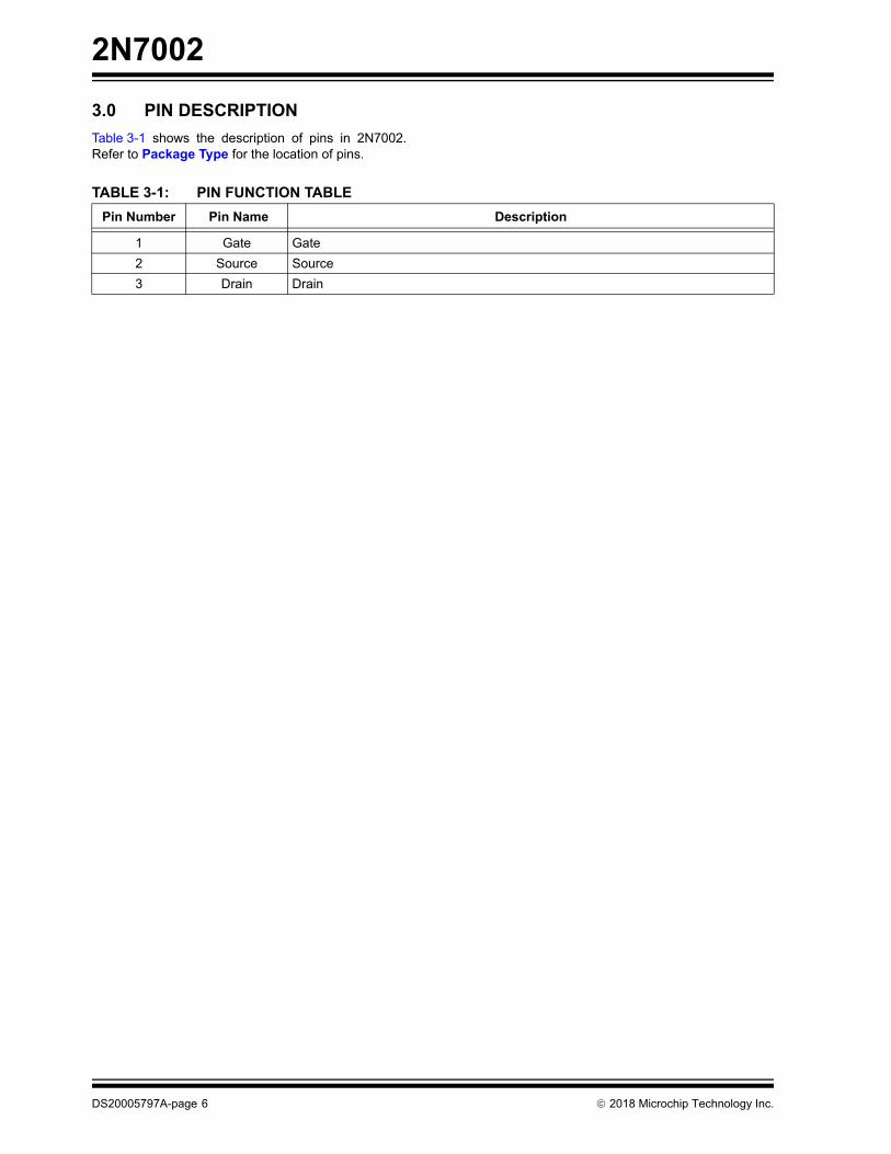
3.0 PIN DESCRIPTION
Table 3-1 shows the description of pins in 2N7002. Refer to Package Type for the location of pins.
TABLE 3-1: PIN FUNCTION TABLE
Pin Number Pin Name Description
1 Gate Gate
2 Source Source
3 Drain Drain
DS20005797A-page 6 2018 Microchip Technology Inc.
2N7002
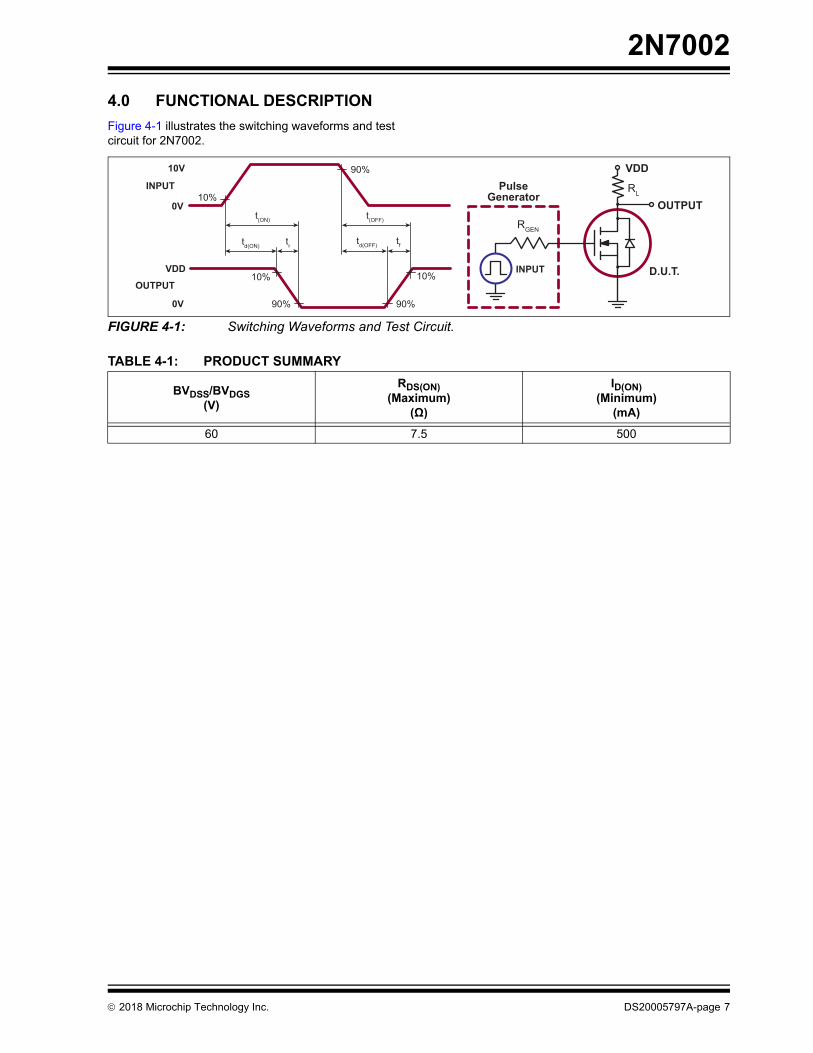
4.0 FUNCTIONAL DESCRIPTION
Figure 4-1 illustrates the switching waveforms and test circuit for 2N7002.
90%
10%
90% 90%
10%10%
PulseGenerator
VDD
RL
OUTPUT
D.U.T.
t(ON)
td(ON)
t(OFF)
td(OFF)tr
INPUT
INPUT
OUTPUT
10V
VDD
RGEN
0V
0V
tf
FIGURE 4-1: Switching Waveforms and Test Circuit.
TABLE 4-1: PRODUCT SUMMARY
BVDSS/BVDGS(V)
RDS(ON)(Maximum)
(Ω)
ID(ON)(Minimum)
(mA)
60 7.5 500
2018 Microchip Technology Inc. DS20005797A-page 7
2N7002
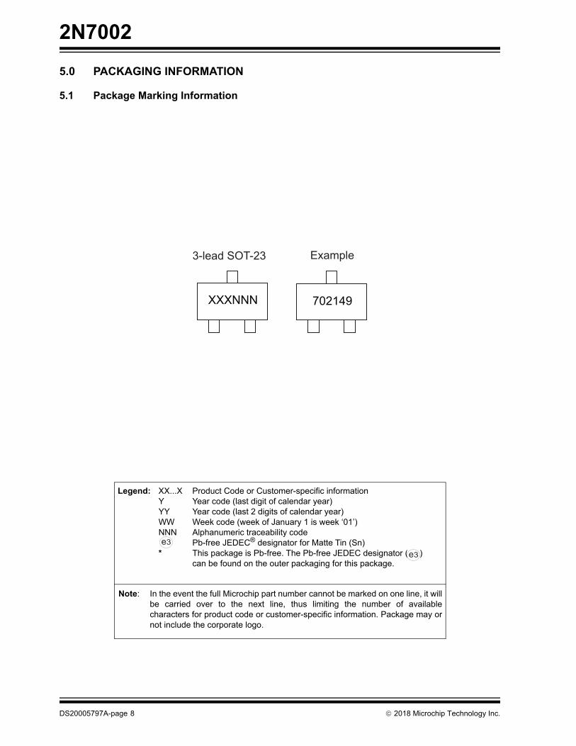
5.0 PACKAGING INFORMATION
5.1 Package Marking Information
Legend: XX...X Product Code or Customer-specific informationY Year code (last digit of calendar year)YY Year code (last 2 digits of calendar year)WW Week code (week of January 1 is week ‘01’)NNN Alphanumeric traceability code Pb-free JEDEC® designator for Matte Tin (Sn)* This package is Pb-free. The Pb-free JEDEC designator ( )
can be found on the outer packaging for this package.
Note: In the event the full Microchip part number cannot be marked on one line, it will be carried over to the next line, thus limiting the number of available characters for product code or customer-specific information. Package may or not include the corporate logo.
3e
3e
XXXNNN 702149
3-lead SOT-23 Example
DS20005797A-page 8 2018 Microchip Technology Inc.
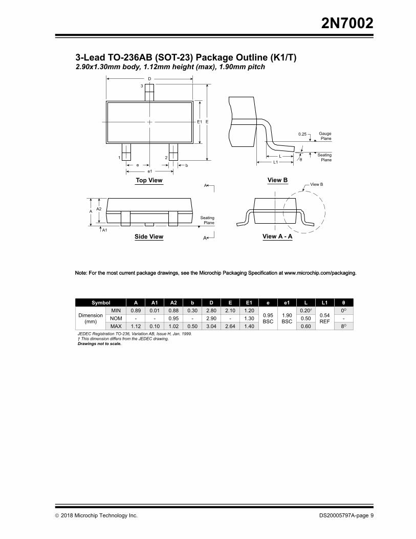
2N7002
3-Lead TO-236AB (SOT-23) Package Outline (K1/T)2.90x1.30mm body, 1.12mm height (max), 1.90mm pitch
Symbol A A1 A2 b D E E1 e e1 L L1
Dimension(mm)
MIN 0.89 0.01 0.88 0.30 2.80 2.10 1.200.95BSC
1.90BSC
0.20†
0.54REF
0O
NOM - - 0.95 - 2.90 - 1.30 0.50 -MAX 1.12 0.10 1.02 0.50 3.04 2.64 1.40 0.60 8O
JEDEC Registration TO-236, Variation AB, Issue H, Jan. 1999.† This dimension differs from the JEDEC drawing.Drawings not to scale.
View B
View A - ASide View
Top ViewView B
GaugePlane
SeatingPlane
0.25
L1L
E1 E
D
3
1 2
ee1
b
A
A
SeatingPlane
A A2
A1
Note: For the most current package drawings, see the Microchip Packaging Specification at www.microchip.com/packaging.Note: For the most current package drawings, see the Microchip Packaging Specification at www.microchip.com/packaging.
2018 Microchip Technology Inc. DS20005797A-page 9
2N7002
NOTES:
DS20005797A-page 10 2018 Microchip Technology Inc.
2018 Microchip Technology Inc. DS20005797A-page 11
2N7002
APPENDIX A: REVISION HISTORY
Revision A (September 2018)
• Converted Supertex Doc# DSFP-2N7002 to Microchip DS20005797A
• Changed the package marking format
• Added some sections to comply with standard Microchip Technology documentation format
• Made minor text changes throughout the docu-ment
2N7002
DS20005797A-page 12 2018 Microchip Technology Inc.
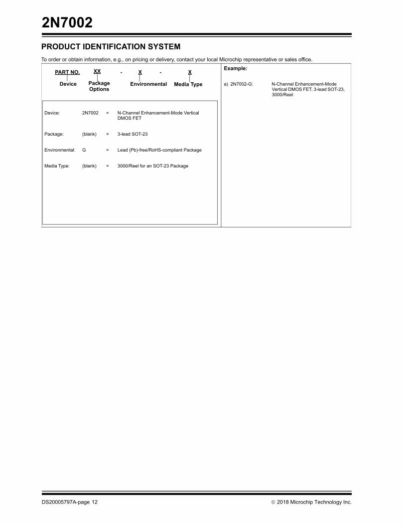
PRODUCT IDENTIFICATION SYSTEM
To order or obtain information, e.g., on pricing or delivery, contact your local Microchip representative or sales office.
Example:
a) 2N7002-G: N-Channel Enhancement-Mode Vertical DMOS FET, 3-lead SOT-23, 3000/Reel
PART NO.
Device
Device: 2N7002 = N-Channel Enhancement-Mode Vertical DMOS FET
Package: (blank) = 3-lead SOT-23
Environmental: G = Lead (Pb)-free/RoHS-compliant Package
Media Type: (blank) = 3000/Reel for an SOT-23 Package
XX
Package
- X - X
Environmental Media Type Options
Note the following details of the code protection feature on Microchip devices:
• Microchip products meet the specification contained in their particular Microchip Data Sheet.
• Microchip believes that its family of products is one of the most secure families of its kind on the market today, when used in the intended manner and under normal conditions.
• There are dishonest and possibly illegal methods used to breach the code protection feature. All of these methods, to our knowledge, require using the Microchip products in a manner outside the operating specifications contained in Microchip’s Data Sheets. Most likely, the person doing so is engaged in theft of intellectual property.
• Microchip is willing to work with the customer who is concerned about the integrity of their code.
• Neither Microchip nor any other semiconductor manufacturer can guarantee the security of their code. Code protection does not mean that we are guaranteeing the product as “unbreakable.”
Code protection is constantly evolving. We at Microchip are committed to continuously improving the code protection features of our products. Attempts to break Microchip’s code protection feature may be a violation of the Digital Millennium Copyright Act. If such acts allow unauthorized access to your software or other copyrighted work, you may have a right to sue for relief under that Act.
Information contained in this publication regarding device applications and the like is provided only for your convenience and may be superseded by updates. It is your responsibility to ensure that your application meets with your specifications. MICROCHIP MAKES NO REPRESENTATIONS OR WARRANTIES OF ANY KIND WHETHER EXPRESS OR IMPLIED, WRITTEN OR ORAL, STATUTORY OR OTHERWISE, RELATED TO THE INFORMATION, INCLUDING BUT NOT LIMITED TO ITS CONDITION, QUALITY, PERFORMANCE, MERCHANTABILITY OR FITNESS FOR PURPOSE. Microchip disclaims all liability arising from this information and its use. Use of Microchip devices in life support and/or safety applications is entirely at the buyer’s risk, and the buyer agrees to defend, indemnify and hold harmless Microchip from any and all damages, claims, suits, or expenses resulting from such use. No licenses are conveyed, implicitly or otherwise, under any Microchip intellectual property rights unless otherwise stated.
2018 Microchip Technology Inc.
Microchip received ISO/TS-16949:2009 certification for its worldwide headquarters, design and wafer fabrication facilities in Chandler and Tempe, Arizona; Gresham, Oregon and design centers in California and India. The Company’s quality system processes and procedures are for its PIC® MCUs and dsPIC® DSCs, KEELOQ® code hopping devices, Serial EEPROMs, microperipherals, nonvolatile memory and analog products. In addition, Microchip’s quality system for the design and manufacture of development systems is ISO 9001:2000 certified.
QUALITYMANAGEMENTSYSTEMCERTIFIEDBYDNV
== ISO/TS16949==
Trademarks
The Microchip name and logo, the Microchip logo, AnyRate, AVR, AVR logo, AVR Freaks, BitCloud, chipKIT, chipKIT logo, CryptoMemory, CryptoRF, dsPIC, FlashFlex, flexPWR, Heldo, JukeBlox, KeeLoq, Kleer, LANCheck, LINK MD, maXStylus, maXTouch, MediaLB, megaAVR, MOST, MOST logo, MPLAB, OptoLyzer, PIC, picoPower, PICSTART, PIC32 logo, Prochip Designer, QTouch, SAM-BA, SpyNIC, SST, SST Logo, SuperFlash, tinyAVR, UNI/O, and XMEGA are registered trademarks of Microchip Technology Incorporated in the U.S.A. and other countries.
ClockWorks, The Embedded Control Solutions Company, EtherSynch, Hyper Speed Control, HyperLight Load, IntelliMOS, mTouch, Precision Edge, and Quiet-Wire are registered trademarks of Microchip Technology Incorporated in the U.S.A.
Adjacent Key Suppression, AKS, Analog-for-the-Digital Age, Any Capacitor, AnyIn, AnyOut, BodyCom, CodeGuard, CryptoAuthentication, CryptoAutomotive, CryptoCompanion, CryptoController, dsPICDEM, dsPICDEM.net, Dynamic Average Matching, DAM, ECAN, EtherGREEN, In-Circuit Serial Programming, ICSP, INICnet, Inter-Chip Connectivity, JitterBlocker, KleerNet, KleerNet logo, memBrain, Mindi, MiWi, motorBench, MPASM, MPF, MPLAB Certified logo, MPLIB, MPLINK, MultiTRAK, NetDetach, Omniscient Code Generation, PICDEM, PICDEM.net, PICkit, PICtail, PowerSmart, PureSilicon, QMatrix, REAL ICE, Ripple Blocker, SAM-ICE, Serial Quad I/O, SMART-I.S., SQI, SuperSwitcher, SuperSwitcher II, Total Endurance, TSHARC, USBCheck, VariSense, ViewSpan, WiperLock, Wireless DNA, and ZENA are trademarks of Microchip Technology Incorporated in the U.S.A. and other countries.
SQTP is a service mark of Microchip Technology Incorporated in the U.S.A.
Silicon Storage Technology is a registered trademark of Microchip Technology Inc. in other countries.
GestIC is a registered trademark of Microchip Technology Germany II GmbH & Co. KG, a subsidiary of Microchip Technology Inc., in other countries.
All other trademarks mentioned herein are property of their respective companies.
© 2018, Microchip Technology Incorporated, All Rights Reserved.
ISBN: 978-1-5224-3477-1
DS20005797A-page 13

DS20005797A-page 14 2018 Microchip Technology Inc.
AMERICASCorporate Office2355 West Chandler Blvd.Chandler, AZ 85224-6199Tel: 480-792-7200 Fax: 480-792-7277Technical Support: http://www.microchip.com/supportWeb Address: www.microchip.com
AtlantaDuluth, GA Tel: 678-957-9614 Fax: 678-957-1455
Austin, TXTel: 512-257-3370
BostonWestborough, MA Tel: 774-760-0087 Fax: 774-760-0088
ChicagoItasca, IL Tel: 630-285-0071 Fax: 630-285-0075
DallasAddison, TX Tel: 972-818-7423 Fax: 972-818-2924
DetroitNovi, MI Tel: 248-848-4000
Houston, TX Tel: 281-894-5983
IndianapolisNoblesville, IN Tel: 317-773-8323Fax: 317-773-5453Tel: 317-536-2380
Los AngelesMission Viejo, CA Tel: 949-462-9523Fax: 949-462-9608Tel: 951-273-7800
Raleigh, NC Tel: 919-844-7510
New York, NY Tel: 631-435-6000
San Jose, CA Tel: 408-735-9110Tel: 408-436-4270
Canada - TorontoTel: 905-695-1980 Fax: 905-695-2078
ASIA/PACIFICAustralia - SydneyTel: 61-2-9868-6733
China - BeijingTel: 86-10-8569-7000
China - ChengduTel: 86-28-8665-5511
China - ChongqingTel: 86-23-8980-9588
China - DongguanTel: 86-769-8702-9880
China - GuangzhouTel: 86-20-8755-8029
China - HangzhouTel: 86-571-8792-8115
China - Hong Kong SARTel: 852-2943-5100
China - NanjingTel: 86-25-8473-2460
China - QingdaoTel: 86-532-8502-7355
China - ShanghaiTel: 86-21-3326-8000
China - ShenyangTel: 86-24-2334-2829
China - ShenzhenTel: 86-755-8864-2200
China - SuzhouTel: 86-186-6233-1526
China - WuhanTel: 86-27-5980-5300
China - XianTel: 86-29-8833-7252
China - XiamenTel: 86-592-2388138
China - ZhuhaiTel: 86-756-3210040
ASIA/PACIFICIndia - BangaloreTel: 91-80-3090-4444
India - New DelhiTel: 91-11-4160-8631
India - PuneTel: 91-20-4121-0141
Japan - OsakaTel: 81-6-6152-7160
Japan - TokyoTel: 81-3-6880- 3770
Korea - DaeguTel: 82-53-744-4301
Korea - SeoulTel: 82-2-554-7200
Malaysia - Kuala LumpurTel: 60-3-7651-7906
Malaysia - PenangTel: 60-4-227-8870
Philippines - ManilaTel: 63-2-634-9065
SingaporeTel: 65-6334-8870
Taiwan - Hsin ChuTel: 886-3-577-8366
Taiwan - KaohsiungTel: 886-7-213-7830
Taiwan - TaipeiTel: 886-2-2508-8600
Thailand - BangkokTel: 66-2-694-1351
Vietnam - Ho Chi MinhTel: 84-28-5448-2100
EUROPEAustria - WelsTel: 43-7242-2244-39Fax: 43-7242-2244-393
Denmark - CopenhagenTel: 45-4450-2828 Fax: 45-4485-2829
Finland - EspooTel: 358-9-4520-820
France - ParisTel: 33-1-69-53-63-20 Fax: 33-1-69-30-90-79
Germany - GarchingTel: 49-8931-9700
Germany - HaanTel: 49-2129-3766400
Germany - HeilbronnTel: 49-7131-67-3636
Germany - KarlsruheTel: 49-721-625370
Germany - MunichTel: 49-89-627-144-0 Fax: 49-89-627-144-44
Germany - RosenheimTel: 49-8031-354-560
Israel - Ra’anana Tel: 972-9-744-7705
Italy - Milan Tel: 39-0331-742611 Fax: 39-0331-466781
Italy - PadovaTel: 39-049-7625286
Netherlands - DrunenTel: 31-416-690399 Fax: 31-416-690340
Norway - TrondheimTel: 47-7288-4388
Poland - WarsawTel: 48-22-3325737
Romania - BucharestTel: 40-21-407-87-50
Spain - MadridTel: 34-91-708-08-90Fax: 34-91-708-08-91
Sweden - GothenbergTel: 46-31-704-60-40
Sweden - StockholmTel: 46-8-5090-4654
UK - WokinghamTel: 44-118-921-5800Fax: 44-118-921-5820
Worldwide Sales and Service
08/15/18
Related Documents