International Journal of Advances in Engineering & Technology, May, 2014. ©IJAET ISSN: 22311963 308 Vol. 7, Issue 2, pp. 308-317 A NEW ADDITION DESIGN PRINCIPLE BASED ON TERNARY OPTICAL PROCESSOR Alaa A. Al-Saffar and Qabeela Q. Thabit Foundation of Technical Education, Basrah Technical College, Basrah City, Iraq Department of Electrical Engineering, Basrah University, Basrah City, Iraq ABSTRACT A three-step Ternary optical modified signed digit (MSD) adder is proposed based on decrease-radix design principle (DRDP) which constructs all dualistic ternary logic operators. In this present work all optical scheme of the different ternary logical states are represented by vertical and horizontal polarized state of light. The basic operational unit (BOU) of the adder is implemented with LCD, vertical and horizontal polarizer and suitable control circuit (CC). Optical tri-state gates has been used in the control circuit to have minimal number of BOUs. To further reducing the number of BOUs, pipeline principle has been successfully used in (n+2) cycles to get the final results of two arrays MSD numbers where n is the number of elements in each array. Theoretical design is presented and verified through numerical simulation of the three steps of the MSD addition. The method promises both accuracy and higher processing speed. KEYWORDS: Ternary optical computer(TOC), decrease-radix design principle (DRDP), modified signed- digit numbers (MSD), basic operation units (BOUs), polarizer light, addition operation, and liquid crystal. I. INTRODUCTION The advent of digital-computing techniques has already produced tremendous increases in speed, accuracy , and flexibility over analog-computing techniques. However, digital computing is constrained mainly by Von Neumann interconnection bottleneck, which makes the computation process inherently sequential in nature [1]. Optical computing provides an attractive approach of attaining ultra-high- speed computing since it can process enormous amounts of data in parallel, at a high speed, with high temporal/spatial bandwidth and non-interfering communications [2]. Several nonbinary-number representation schemes, such as multiple-valued fixed radix-number, residue-number, redundant- number, and signed-digit-number representations have been reported in the past decade to increase the speed of computation and to implement these nonbinary-based arithmetic operations digitally and optically. Signed-digit number representations limit carry propagation to one (two) positions to the left during the operations of addition(subtraction) in digital computers. The carry-propagation chains are eliminated by use of redundant representation for operands [3]. In 2000, Jin Yi proposed a new optical computer structure ternary optical computer using light intensity and polarization to denote ternary value:0, 1, 2[4]. In early 2007, Yan JunYang, Jin Yi, and Kaizhong find the rule of multi-valued logic processor and setup the DRDP [5]. After that in 2010, Jin Yi et al. proposed the principle and organization of modified signed-digit (MSD) adder, and designed the MSD adder for TOC [6]. In 2011, Ouyang Shan et al. ternary optical processor TOP construction via the reconfiguration circuit, to an operator demanded byusers dynamically, and namely the limited optical hardware resource can be reused to construct any one of the 19 683 two-input tri-value logic operators [7, 8]. The design of an all-optical system for some basic tri-state logic operations (trinary OR, trinary AND, trinary XOR, Inverter (IN), Truth detector (TD), False detector (FD)) which exploits the polarization properties of light. Nonlinear material based optical switch can play an important role. Tri-state logic can play a significant role towards carry and borrow free arithmetic operations [9, 10].

Welcome message from author
This document is posted to help you gain knowledge. Please leave a comment to let me know what you think about it! Share it to your friends and learn new things together.
Transcript
International Journal of Advances in Engineering & Technology, May, 2014.
©IJAET ISSN: 22311963
308 Vol. 7, Issue 2, pp. 308-317
A NEW ADDITION DESIGN PRINCIPLE BASED ON TERNARY
OPTICAL PROCESSOR
Alaa A. Al-Saffar and Qabeela Q. Thabit Foundation of Technical Education, Basrah Technical College, Basrah City, Iraq
Department of Electrical Engineering, Basrah University, Basrah City, Iraq
ABSTRACT A three-step Ternary optical modified signed digit (MSD) adder is proposed based on decrease-radix design
principle (DRDP) which constructs all dualistic ternary logic operators. In this present work all optical scheme
of the different ternary logical states are represented by vertical and horizontal polarized state of light. The
basic operational unit (BOU) of the adder is implemented with LCD, vertical and horizontal polarizer and
suitable control circuit (CC). Optical tri-state gates has been used in the control circuit to have minimal number
of BOUs. To further reducing the number of BOUs, pipeline principle has been successfully used in (n+2)
cycles to get the final results of two arrays MSD numbers where n is the number of elements in each array.
Theoretical design is presented and verified through numerical simulation of the three steps of the MSD
addition. The method promises both accuracy and higher processing speed.
KEYWORDS: Ternary optical computer(TOC), decrease-radix design principle (DRDP), modified signed-
digit numbers (MSD), basic operation units (BOUs), polarizer light, addition operation, and liquid crystal.
I. INTRODUCTION
The advent of digital-computing techniques has already produced tremendous increases in speed,
accuracy , and flexibility over analog-computing techniques. However, digital computing is constrained
mainly by Von Neumann interconnection bottleneck, which makes the computation process inherently
sequential in nature [1]. Optical computing provides an attractive approach of attaining ultra-high-
speed computing since it can process enormous amounts of data in parallel, at a high speed, with high
temporal/spatial bandwidth and non-interfering communications [2]. Several nonbinary-number
representation schemes, such as multiple-valued fixed radix-number, residue-number, redundant-
number, and signed-digit-number representations have been reported in the past decade to increase the
speed of computation and to implement these nonbinary-based arithmetic operations digitally and
optically. Signed-digit number representations limit carry propagation to one (two) positions to the left
during the operations of addition(subtraction) in digital computers. The carry-propagation chains are
eliminated by use of redundant representation for operands [3]. In 2000, Jin Yi proposed a new optical
computer structure ternary optical computer using light intensity and polarization to denote ternary
value:0, 1, 2[4]. In early 2007, Yan JunYang, Jin Yi, and Kaizhong find the rule of multi-valued logic
processor and setup the DRDP [5]. After that in 2010, Jin Yi et al. proposed the principle and
organization of modified signed-digit (MSD) adder, and designed the MSD adder for TOC [6]. In 2011,
Ouyang Shan et al. ternary optical processor TOP construction via the reconfiguration circuit, to an
operator demanded byusers dynamically, and namely the limited optical hardware resource can be
reused to construct any one of the 19 683 two-input tri-value logic operators [7, 8]. The design of an
all-optical system for some basic tri-state logic operations (trinary OR, trinary AND, trinary XOR,
Inverter (IN), Truth detector (TD), False detector (FD)) which exploits the polarization properties of
light. Nonlinear material based optical switch can play an important role. Tri-state logic can play a
significant role towards carry and borrow free arithmetic operations [9, 10].
International Journal of Advances in Engineering & Technology, May, 2014.
©IJAET ISSN: 22311963
309 Vol. 7, Issue 2, pp. 308-317
The main aim of this study is to get suitable design, the control circuit is employed in a new form to
obtain less number of basic operation units BOUs which are used in addition operation. We attempt to
rise the performance of TOP to higher level comparison with the previous design, some developments
have been added in order to obtain an efficient design. In this paper three-step MSD addition optical
TOC structure is presented based on DRDP principle. The paper is organized as follows. In Section II
design principle of DRDP, the structure of the ternary optical processor and the three-step addition
algorithm are discussed. Section III explains with suitable tables the correct operation of the addition.
Section IV discusses simulation results of two MSD arrays and discussion. Section V discusses
conclusion and suggests a roadmap for future works.
II. EXPERIMENTAL MATERIALS AND PROCEDURE
A. Decrease-Radix Design Principle (DRDP)
The principle of decrease-radix design principle for making multi-valued logic unit, which proposed
by Prof. Yi Jin and his PhD candidates Yan Jun-Yong and Zuo Kaizhong, gives a technological guide
for the design of multi-valued computer and become the fundamental theory of ternary optical
computer. The main conclusion of the decrease-radix design theory, is that , if the D-state is include
as one of the n physical states (n >1) for information representation, then each of the 2-input, n-valued
logic operators without carry generation (referred to as an n-valued logic operator in the sequel), can
be constructed from no more than nx(n-1) singleton basic operation units (singleton BOUs)following
a determinate procedure, with up to n x n x (n-1) types of singleton BOUs. The total number of
different 2-input n-valued logic operators is known to be n(nxn)[5,11].
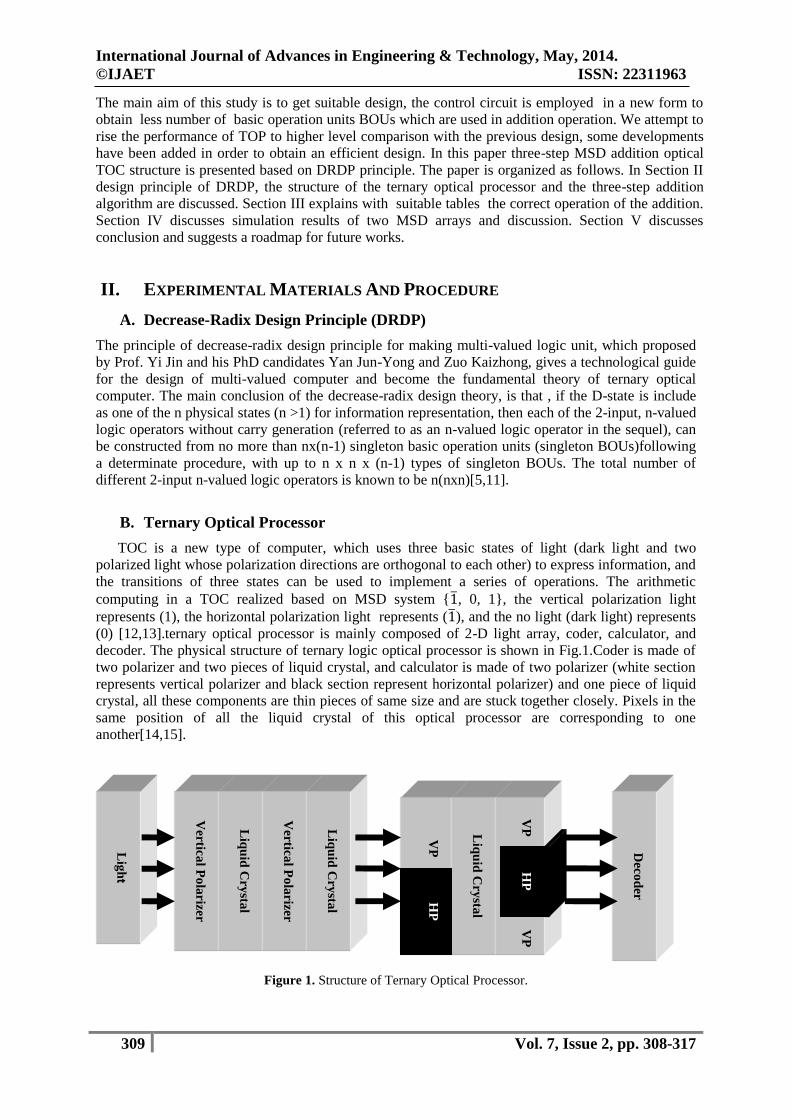
B. Ternary Optical Processor
TOC is a new type of computer, which uses three basic states of light (dark light and two
polarized light whose polarization directions are orthogonal to each other) to express information, and
the transitions of three states can be used to implement a series of operations. The arithmetic
computing in a TOC realized based on MSD system {1̅, 0, 1}, the vertical polarization light
represents (1), the horizontal polarization light represents (1̅), and the no light (dark light) represents
(0) [12,13].ternary optical processor is mainly composed of 2-D light array, coder, calculator, and
decoder. The physical structure of ternary logic optical processor is shown in Fig.1.Coder is made of
two polarizer and two pieces of liquid crystal, and calculator is made of two polarizer (white section
represents vertical polarizer and black section represent horizontal polarizer) and one piece of liquid
crystal, all these components are thin pieces of same size and are stuck together closely. Pixels in the
same position of all the liquid crystal of this optical processor are corresponding to one
another[14,15].
Figure 1. Structure of Ternary Optical Processor.
Lig
ht
Ver
tical P
ola
rizer
Liq
uid
Cry
stal
Ver
tical P
ola
rizer
Liq
uid
Cry
stal
VP
Liq
uid
Cry
stal
VP
VP
Dec
od
er
HP
HP
International Journal of Advances in Engineering & Technology, May, 2014.
©IJAET ISSN: 22311963
310 Vol. 7, Issue 2, pp. 308-317
C. Three-Step Algorithm for MSD Addition Operation
MSD was proposed by Avizienis in 1961[16], and was first used on optical computing by
Draker in 1986. A number x can be represented in MSD by the following equation:
X=∑ 𝑥𝑖2𝑖 𝑥𝑖 ∈ { ̅1,0,1} (1)
𝑖 Suppose the MSD representation of augends X and addend Y are :-
XMSD = Xn-1,…., Xi, …..., X0. Table 4. Truth Table of W'-Transformation.
YMSD = Yn-1,….., Yi, …..., Y0. The three-step addition is performed according to the following:-
Step 1: The T- transformation (carry) and W- transformation (sum) on every couple of bits of Xi and
Yi of the MSD addition are shown in Table 1 and Table 2, respectively[17,18].
Compute Xi + Yi = 2Ti+1 + Wi (i=0, ….., n-1). (2)
Table 1.Truth Table of T-Transformation. Table 2. Truth Table of W-Transformation.
T 1 0 �̅�
1 1 1 0
0 1 0 �̅�
�̅� 0 �̅� �̅�
Step 2: The T'-transformation and W'-transformation on every couple of bits of Ti and Wi, we get
T'i+1 and W'i as shown in Table 3 and Table 4, respectively.
Compute Ti + Wi = 2T'i+1 + W'i (i=0, ….., n-1) (3)
Table 3. Truth Table of T'-Transformation. Table 4. Truth Table of W'-Transformation.
Step 3: The truth table of final sum Si on every couple of bits of T'i and W'i is seen as the
T-transformation shown in Table 1.
Compute Si = W'i + T'i (i=0, ….., n-1) (4)
W 1 0 �̅�
1 0 �̅� 0
0 �̅� 0 1
�̅� 0 1 0
W' 1 0 �̅�
1 0 1 0
0 1 0 �̅�
�̅� 0 �̅� 0
T' 1 0 �̅�
1 1 0 0
0 0 0 0
�̅� 0 0 �̅�
International Journal of Advances in Engineering & Technology, May, 2014.
©IJAET ISSN: 22311963
311 Vol. 7, Issue 2, pp. 308-317
III. NEW DESIGN OF OPTICAL ADDER USING A TERNARY OPTICAL
PROCESSOR
The use of the optical tri-state gates has been suggested as away to eliminate the number of BOUs
which are considering the main component of control circuit. The arithmetic operations form the
largest field of computer optical arithmetic which operates on one or more operands depending on the
operation. The operation is selected from allowable set, which is usually includes addition,
subtraction, multiplication, division, and so on. Addition process for two operands which is an
arithmetic operation has three steps to be calculated, obtained intermediate results and then compute
final sum. The main problem with addition operation is the word length from side and the circuit
complexity in the other side, therefore, we will focus on designing an efficient signed-digit adder for
two or more operands.
Step One of Design:
T-Transformation:
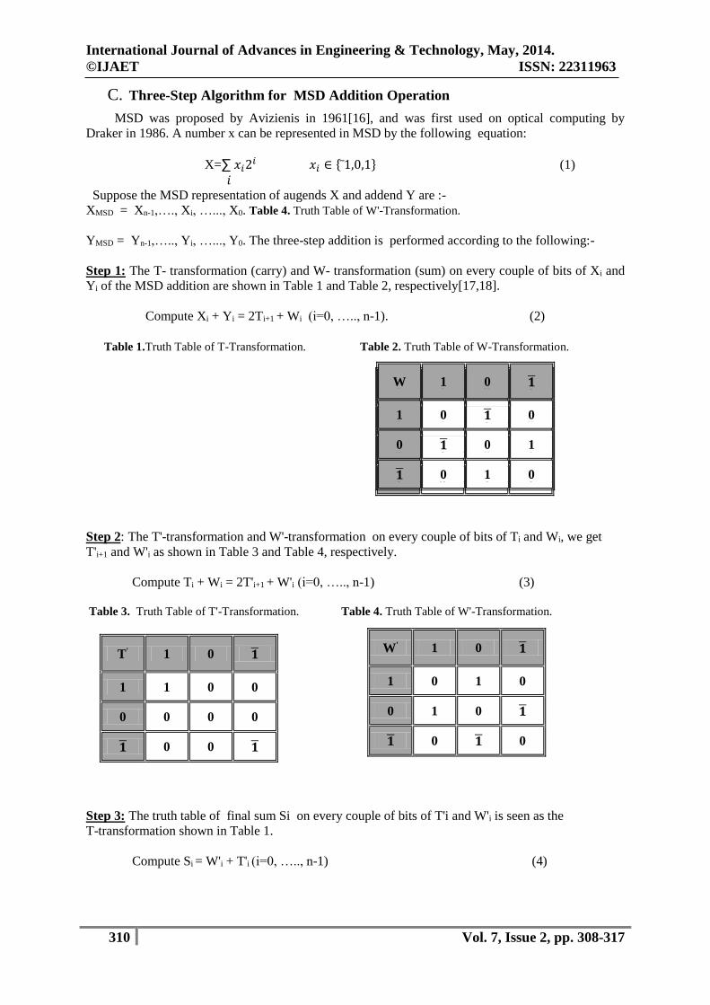
By using tri-state optical gates (OR & False Detector FD) with suitable design, the three cases
combinations{(1+1), (1+0), and (0+1)} can be implemented using one BOU as shown in Fig. 2. The
output of this circuit is equal to 1 only for the combinations{ (1+1) or (1+0) or (0+1)}. While the
three cases combinations{(1̅+1̅), (1̅+0), and (0+1̅)} is constructed based on single BOU by using tri-
state optical gates (OR & Truth Detector TD) with suitable design. The three cases
combination{(1̅+1̅), (1̅+0), and (0+1̅)} can be implemented as shown in Fig. 3. The output of this
circuit is equal to 1̅ only for the combination{(1̅+1̅) or (1̅+0) or (0+1̅)}. The two BOUs are
accumulated to form adder in step one (T-transformation ) as shown in Fig. 2. Note that only one sub-
output (t1, and t2) is activated for any combination of the inputs.
Figure 2. Structure of ATOP for Addition Operation.
(T-Transformation of Step One Addition).
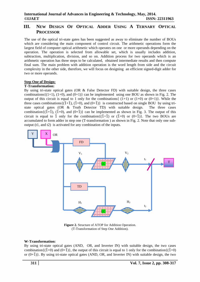
W-Transformation: By using tri-state optical gates (AND, OR, and Inverter IN) with suitable design, the two cases
combination{(1̅+0) and (0+1̅)}, the output of this circuit is equal to 1 only for the combination{(1̅+0)
or (0+1̅)}. By using tri-state optical gates (AND, OR, and Inverter IN) with suitable design, the two
OR
2t
1t
2V
1H
1V
LC
LC
2H
TD
FD
T
X Y
International Journal of Advances in Engineering & Technology, May, 2014.
©IJAET ISSN: 22311963
312 Vol. 7, Issue 2, pp. 308-317
cases combination{(1+0) and (0+1)}, the output of this circuit is equal to 1̅ only for the combination
{(1+0) or (0+1)}. The two BOUs are accumulated to form adder in step one (W-transformation ) as
shown in Fig. 3. Note that only one sub-output (w1 and w2) is activated for any combination of the
inputs.
Figure 3. Structure of MTOP for Addition Operation.
(W-Transformation of Step One Addition ).
Step Two of Design:
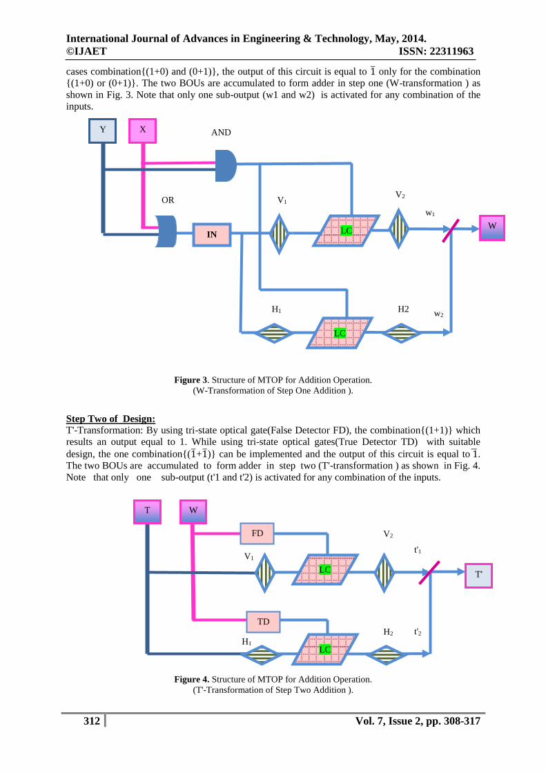
T'-Transformation: By using tri-state optical gate(False Detector FD), the combination{(1+1)} which
results an output equal to 1. While using tri-state optical gates(True Detector TD) with suitable
design, the one combination{(1̅+1̅)} can be implemented and the output of this circuit is equal to 1̅.
The two BOUs are accumulated to form adder in step two (T'-transformation ) as shown in Fig. 4.
Note that only one sub-output (t'1 and t'2) is activated for any combination of the inputs.
Figure 4. Structure of MTOP for Addition Operation.
(T'-Transformation of Step Two Addition ).
2t'
2w
2V 1V
H2 1H
LC
LC
X Y
W
1w
IN
AND
OR
2V
1V
1H 2H
LC
FD
LC
TD
TD
T W
T'
1t'
International Journal of Advances in Engineering & Technology, May, 2014.
©IJAET ISSN: 22311963
313 Vol. 7, Issue 2, pp. 308-317
Step Three of Design : The structure and components of step three (T- transformation ) are the same
as (T-transformation) in step one.
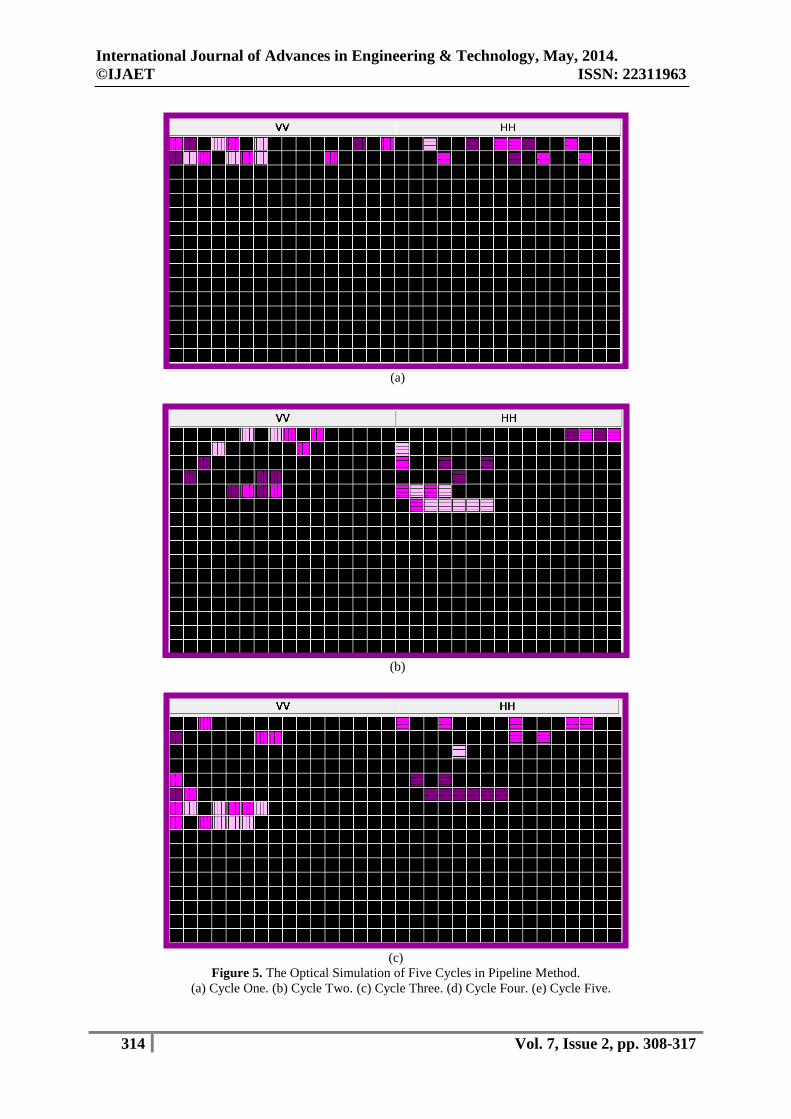
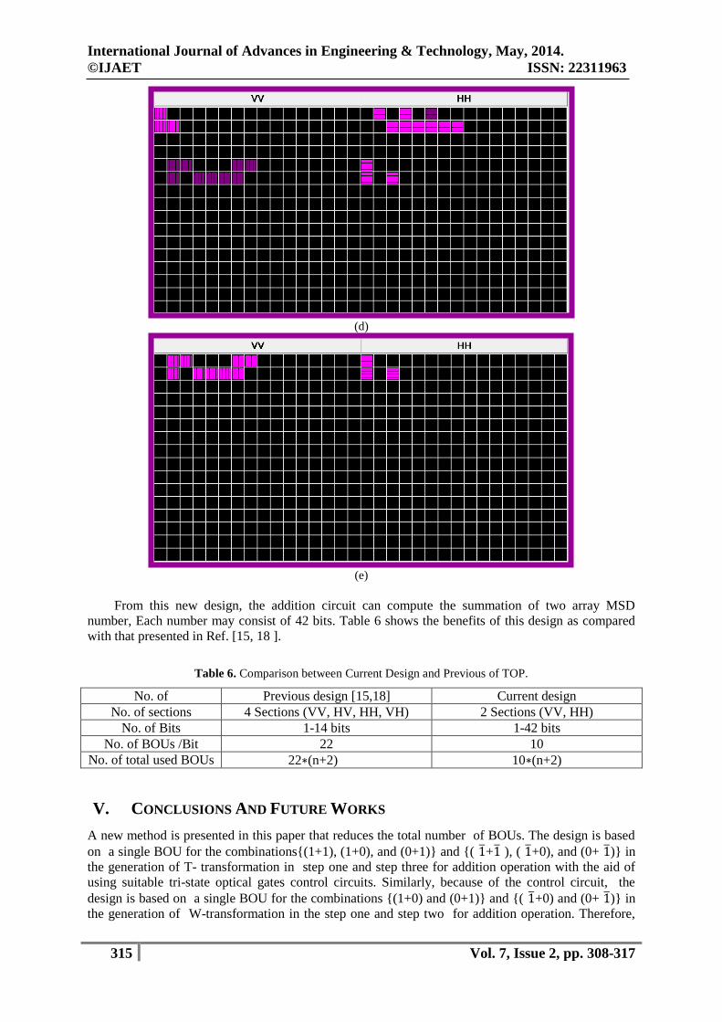
IV. SIMULATION RESULTS
Optical Simulation of Three-Step Adder : The number of BOUs in this method depends only on the
number bits in each operand. Therefore, the number of BOUs is calculated as in Eq.(5):-
B = 10 x (n + 2)
Where B:Number of basic operation units
n: Number of bits in each operands
Example:- For the following addition operation:-
B. + =
C.
The addition operation consists of five cycles as shown in Table 5. The total numbers of the used
BOUs in this design is equal to (238) for the five cycles. The optical simulation of the five cycles is
shown in Fig. 5:
Table 5. The Three-Step of Addition Operation for the Five Cycles That are used to get the Final Results.
No. of Cycle
Step One
Step Two
Step Three
Cycle 1 X1 + Y1 ---------- ----------
Cycle 2 X2 + Y2 T1 + W1 ----------
Cycle 3 X3 + Y3 T2 + W2 T'1 + W'1
Cycle 4 ---------- T3 + W3 T'2 + W'2
Cycle 5 ---------- ---------- T'3 + W'3
MSD)0011011̅011̅10(101
=
+
MSD)1̅1̅1̅1̅1̅1̅010101̅1̅1̅1̅)
MSD)1̅1101̅10111̅01(111
10(21286)
2S
3S
2X
3Y
2Y
3X
10(32767)
1031674)-(
102618)-(
=
1032111)-( +
1X 1Y 1S 10(28117)
MSD1111111111111111))
=
10(49403)
1063785)-(
10(30149)
(5)
+
MSD)1100000100001̅101̅(
MSD1)1̅1̅1̅1̅1̅1̅11001̅01̅01̅(
MSD)11111̅11̅11000111̅(
MSD)1̅11101̅01̅10011̅10)
MSD)1̅1̅1̅1̅1̅0001011̅01̅0)
International Journal of Advances in Engineering & Technology, May, 2014.
©IJAET ISSN: 22311963
314 Vol. 7, Issue 2, pp. 308-317
(a)
(b)
(c)
Figure 5. The Optical Simulation of Five Cycles in Pipeline Method.
(a) Cycle One. (b) Cycle Two. (c) Cycle Three. (d) Cycle Four. (e) Cycle Five.
International Journal of Advances in Engineering & Technology, May, 2014.
©IJAET ISSN: 22311963
315 Vol. 7, Issue 2, pp. 308-317
(d)
(e)
From this new design, the addition circuit can compute the summation of two array MSD
number, Each number may consist of 42 bits. Table 6 shows the benefits of this design as compared
with that presented in Ref. [15, 18 ].
Table 6. Comparison between Current Design and Previous of TOP.
No. of Previous design [15,18] Current design
No. of sections 4 Sections (VV, HV, HH, VH) 2 Sections (VV, HH)
No. of Bits 1-14 bits 1-42 bits
No. of BOUs /Bit 22 10
No. of total used BOUs 22∗(n+2) 10∗(n+2)
V. CONCLUSIONS AND FUTURE WORKS
A new method is presented in this paper that reduces the total number of BOUs. The design is based
on a single BOU for the combinations{(1+1), (1+0), and (0+1)} and {( 1̅+1̅ ), ( 1̅+0), and (0+ 1̅)} in
the generation of T- transformation in step one and step three for addition operation with the aid of
using suitable tri-state optical gates control circuits. Similarly, because of the control circuit, the
design is based on a single BOU for the combinations {(1+0) and (0+1)} and {( 1̅+0) and (0+ 1̅)} in
the generation of W-transformation in the step one and step two for addition operation. Therefore,
International Journal of Advances in Engineering & Technology, May, 2014.
©IJAET ISSN: 22311963
316 Vol. 7, Issue 2, pp. 308-317
the total number of BOUs /bit in this design becomes equal to 10 BOUs/bit. Thus, reducing number
of used BOUs and increasing the speed of operations. We attempt to rise the performance of TOP to
higher level as compared with the design in Ref. [14 ]. The procedure and design used in this paper
can be used for the multiplication operation after computing the partial product results with suitable
design of BOUs. Also, the work can be extended to develop a TOC that can compute the arithmetic
operation of number with higher radix such as trinary and quaternary singed digit numbers (TSD) and
(QSD) by using suitable optical circuit that converts these numbers to MSD numbers.
REFERENCES
[1] M. S. Alam, M. A. Karim, A. A. S. Awwal, and J. J. Westerkamp, Optical processing based on
conditional higher-order trinary modified signed-digit symbolic substitution, App. Opt., 31(26) 5614-
5621. 1992.
[2] J. U. Ahmed, A. A. S. Awwal, and M. A. Karim, Two-bit trinary full adder design based on
restricted signed-digit numbers, Optics & Laser Technology , 26(4) 225-228. 1994.
[3] K. Cherri, M. K. Habib, and M. S. Alam, "Optoelectronic Recoded and Nonrecoded Trinary Signed-
Digit Adder That Uses Optical Correlation", App. Opt., 37(11) 2153-2163. 1998.
[4] J. Yi, H. Hua-Can, and L. Yangtian, "Ternary Optical Computer Principle", Science In China(Series
F), 46( 2) 145-150. April 2003.
[5] Yan Junyong, Jin Yi, and Zuo Kaizhong, "Decrease –Radix Design Principle for Carrying/Borrowing
Free Multi-Valued and Application in Ternary Optical Computer", Science In China(Series F):
Information Sciences, 51 (10) 1415-1426. Oct. 2008.
[6] J. Yi, S. Y. Fu, P. J. Jie, X. S. Yi, D. G. Tai, Y. D. Jian, and Y. H. Hang, "Principle and Construction
of MSD Adder in Ternary Optical Computer", Science China , 53 ( 11) 2159-2168. 2010 .
[7] O. Shan, J. Yi, Z. Yu, and W. Hong-jain, "Principle and Architecture of Parallel Reconfiguration
Circuit for Ternary Optical Computer", JShanghai Univ (Eng Ed), 15 ( 5) 397-404. 2011.
[8] J. Yi, W. Hong-jain, O. Shan, Z. Yu, S. Y. Fu, P. J. Jie, and L. X. Min, "Principle, Structures, and
Implementation of Reconfigurable Ternary Optical Processor", Science China , 54 (11) 2236-2246.
2011.
[9] T. Chattopadhyay, G. K. Maity, and J. N. Roy, "Designing Of All-Optical Tri-State Logic System
with the Help of Optical Nonlinear Material", Journal of Nonlinear Optical Physics & Materials, 17(
3) 315-328. 2008.
[10] P. Bhowmik, T. Chattopadhyay, C. Taraphdar, and J. N. Roy, "Designing of All Optical Circuit for
Two Input Ternary Min Logical Operation", Convergence of Optics and Electronics & JIS College of
Engineering, 94-101. 2011.
[11] Chunzhi Li, and Junyong Yan," Design Method and Implementation of Ternary Logic Optical
Calculator", IFIP AICT , 347. 147-166. 2011.
[12] X. Wang, P. J. Jie, L. Mei, Z. Shen, and O. Shan," Carry Vector-Matrix Multiplication on A
Dynamically Reconfigurable Optical Platform", Applied Optics , 49(12) 2352-2362. 20th April 2010.
[13] Y. Shen, P. Hu, and H. Wang, "The Computational Complexity of Arithmetic Based on Ternary
Optical Computer", Journal of Information & Computational Science , 8 ( 5) 850-857. 2011.
[14] L. Yanping, P. J. Jie, C. Yuanyuan, and H. Hui, "A New Carry-Free Adder Model for Ternary
Optical Computer",10th International Symposium on Distributed Computing and Applications to
Business, Engineering and Science, 6. 64-68. 2011.
[15] H. He, J. Peng, Y. Liu, X. Wang, and K. Song, "Research and Design of A MSD Adder of Ternary
Optical Computer", Springer- V ICAIC-228, 413-420. 2011.
[16] A. Avizienis, "Signed-Digit Number Representation for Fast Parallel Arithmetic", IRE Trans.
Electron. Comput., EC-10, pp. 389-400, 1961.
[17] J. Yi, X. Wang, P. J. Jie, L. Mei, S. Yi, and O. Shan, "Vector-Matrix Multiplication in Ternary
Optical Computer", International Journal of Numerical Analysis and Modeling , 9 ( 2) 401-409.
2012.
[18] X. Wang, P. J. Jie, J. Yi, L. Mei, Z. Shen, and O. Shan, "Vector-Matrix Multiplication Based on
Ternary Optical Computer", In: Proceeding of the 2nd International Conference on High Performance
Computing and Application, Shanghai University, China, 2009.
International Journal of Advances in Engineering & Technology, May, 2014.
©IJAET ISSN: 22311963
317 Vol. 7, Issue 2, pp. 308-317
AUTHORS
Alaa A. Al-Saffar was born in Basrah, Iraq, in 1957. He received the B.Sc, M.Sc and PHD
from the University of Basarh, College of Engineering, Electrical Engineering Department
in 1979, 1982 and 2001, respectively. His current research interests include optical
computing and robotic control.
Qabeela Q. Thabit - She obtained her B. Eng. in Computer Engineering and M. Eng.
degrees Electronics Engineering. from the University of Basrah, College of Engineering in
2004, and 2013, respectively. Her research areas include Computer architecture and optical
Computing .
Related Documents