PN 942615 March 1995 © 1995 Fluke Corporation, Inc. All rights reserved. Printed in U.S.A. All product names are trademarks of their respective companies. ® 2640A/2645A NetDAQ Data Acquisition Tools Service Manual

Welcome message from author
This document is posted to help you gain knowledge. Please leave a comment to let me know what you think about it! Share it to your friends and learn new things together.
Transcript
PN 942615March 1995© 1995 Fluke Corporation, Inc. All rights reserved. Printed in U.S.A.All product names are trademarks of their respective companies. ®
2640A/2645ANetDAQ Data Acquisition Tools
Service Manual

LIMITED WARRANTY & LIMITATION OF LIABILITY
Each Fluke product is warranted to be free from defects in material and workmanship undernormal use and service. The warranty period is one year and begins on the date of shipment.Parts, product repairs and services are warranted for 90 days. This warranty extends only to theoriginal buyer or end-user customer of a Fluke authorized reseller, and does not apply to fuses,disposable batteries or to any product which, in Fluke’s opinion, has been misused, altered,neglected or damaged by accident or abnormal conditions of operation or handling. Flukewarrants that software will operate substantially in accordance with its functional specifications for90 days and that it has been properly recorded on non-defective media. Fluke does not warrantthat software will be error free or operate without interruption.
Fluke authorized resellers shall extend this warranty on new and unused products to end-usercustomers only but have no authority to extend a greater or different warranty on behalf of Fluke.Warranty support is available if product is purchased through a Fluke authorized sales outlet orBuyer has paid the applicable international price. Fluke reserves the right to invoice Buyer forimportation costs of repair/replacement parts when product purchased in one country is submittedfor repair in another country.
Fluke’s warranty obligation is limited, at Fluke’s option, to refund of the purchase price, free ofcharge repair, or replacement of a defective product which is returned to a Fluke authorizedservice center within the warranty period.
To obtain warranty service, contact your nearest Fluke authorized service center or send theproduct, with a description of the difficulty, postage and insurance prepaid (FOB Destination), tothe nearest Fluke authorized service center. Fluke assumes no risk for damage in transit.Following warranty repair, the product will be returned to Buyer, transportation prepaid (FOBDestination). If Fluke determines that the failure was caused by misuse, alteration, accident orabnormal condition of operation or handling, Fluke will provide an estimate of repair costs andobtain authorization before commencing the work. Following repair, the product will be returned tothe Buyer transportation prepaid and the Buyer will be billed for the repair and returntransportation charges (FOB Shipping Point).
THIS WARRANTY IS BUYER’S SOLE AND EXCLUSIVE REMEDY AND IS IN LIEU OF ALLOTHER WARRANTIES, EXPRESS OR IMPLIED, INCLUDING BUT NOT LIMITED TO ANYIMPLIED WARRANTY OF MERCHANTABILITY OR FITNESS FOR A PARTICULAR PURPOSE.FLUKE SHALL NOT BE LIABLE FOR ANY SPECIAL, INDIRECT, INCIDENTAL ORCONSEQUENTIAL DAMAGES OR LOSSES, INCLUDING LOSS OF DATA, WHETHERARISING FROM BREACH OF WARRANTY OR BASED ON CONTRACT, TORT, RELIANCE ORANY OTHER THEORY.
Since some countries or states do not allow limitation of the term of an implied warranty, orexclusion or limitation of incidental or consequential damages, the limitations and exclusions ofthis warranty may not apply to every buyer. If any provision of this Warranty is held invalid orunenforceable by a court of competent jurisdiction, such holding will not affect the validity orenforceability of any other provision.
Fluke Corporation Fluke Europe B.V.P.O. Box 9090 P.O. Box 1186Everett WA 5602 B.D. Eindhoven98206-9090 The Netherlands
5/94
SAFETY TERMS IN THIS MANUAL
This instrument has been designed and tested in accordance with IEC publication1010-1 (1992-1), Safety Requirements for Electrical Measuring, Control and LaboratoryEquipment, and ANSI/ISA-582.01-1994, and CAN/CSA-C22.2 No. 1010.1-92. This UserManual contains information, warning, and cautions that must be followed to ensuresafe operation and to maintain the instrument in a safe condition. Use of this equipmentin a manner not specified herein may impair the protection provided by the equipment.
This instrument is designed for IEC 1010-1 Installation Category II use. It is notdesigned for connection to circuits rated over 4800 VA.
WARNING statements identify conditions or practices that could result in personal injuryor loss of life.
CAUTION statements identify conditions or practices that could result in damage toequipment.
SYMBOLS MARKED ON EQUIPMENT
WARNING Risk of electric shock. Refer to the manual.
GROUND Ground terminal to chassis (earth).
Attention Refer to the manual. This symbol indicates that informationabout usage of a feature is contained in the manual. This symbolappears on the rear panel ground post and by the fuse compartment.
AC POWER SOURCE
The instrument is intended to operate from an ac power source that will not apply morethan 264V ac rms between the supply conductors or between either supply conductorand ground. A protective ground connection by way of the grounding conductor in thepower cord is required for safe operation.
USE THE PROPER FUSE
To avoid fire hazard, for fuse replacement use only the specified unit: 15/100 ampere,250V, time delay.
GROUNDING THE INSTRUMENT
The instrument utilizes controlled overvoltage techniques that require the instrument tobe grounded whenever normal mode or common mode ac voltages or transient voltagesmay occur. The enclosure must be grounded through the grounding conductor of thepower cord, or through the rear panel ground binding post.

USE THE PROPER POWER CORD
Use only the power cord and connector appropriate for the voltage and plugconfiguration in your country.
Use only a power cord that is in good condition.
Refer power cord and connector changes to qualified service personnel.
DO NOT OPERATE IN EXPLOSIVE ATMOSPHERES
To avoid explosion, do not operate the instrument in an atmosphere of explosive gas.
DO NOT REMOVE COVER DURING OPERATION
To avoid personal injury or death, do not remove the instrument cover without firstremoving the power source connected to the rear panel. Do not operate the instrumentwithout the cover properly installed. Normal calibration is accomplished with the coverclosed. Access procedures and the warnings for such procedures are contained in thismanual. Service procedures are for qualified service personnel only.
DO NOT ATTEMPT TO OPERATE IF PROTECTION MAY BE IMPAIRED
If the instrument appears damaged or operates abnormally, protection may be impaired.Do not attempt to operate the instrument under these conditions. Refer all questions ofproper instrument operation to qualified service personnel.
i
Table of Contents
Chapter Title Page
1 Introduction and Specification............................................................ 1-1
1-1. Introduction ............................................................................................ 1-31-2. Options and Accessories ........................................................................ 1-61-3. Instrument Connector Set, 2620A-100 .............................................. 1-61-4. Host Computer Ethernet Interfaces.................................................... 1-61-5. Interconnection Cables and Components........................................... 1-61-6. Operating Instructions ............................................................................ 1-71-7. Organization of the Service Manual....................................................... 1-71-8. Conventions............................................................................................ 1-81-9. Specifications ......................................................................................... 1-81-10. 2640A/2645A Combined Specifications ........................................... 1-81-11. 2640A/2645A General Specifications. .......................................... 1-91-12. 2640A/2645A Environmental Specifications................................ 1-101-13. 2640A/2645A Input/Output Capabilities....................................... 1-101-18. 2640A/2645A Totalizer ................................................................. 1-121-19. 2640A/2645A Real-Time Clock and Calendar.............................. 1-121-20. 2640A Specifications ......................................................................... 1-131-21. 2640A DC Voltage Measurement Specifications.......................... 1-131-22. 2640A AC Voltage Measurement Specifications.......................... 1-141-23. 2640A Four-Wire Resistance Measurement Specifications.......... 1-161-24. 2640A Two-Wire Resistance Measurement Specifications .......... 1-161-25. 2640A Four-Wire RTD per ITS-1990 Measurement
Specifications.............................................. .................................. 1-171-26. 2640A Two-Wire RTD per ITS-1990 Measurement
Specifications.............................................. .................................. 1-171-27. 2640A Thermocouple per ITS-1990 Measurement
Specifications.............................................. .................................. 1-181-28. 2640A Frequency Measurement Specifications ............................ 1-191-29. 2645A Specifications ......................................................................... 1-201-30. 2645A DC Voltage Measurement Specifications.......................... 1-201-31. 2645A AC Voltage Measurement Specifications.......................... 1-211-32. 2645A Four-Wire Resistance Measurement Specifications.......... 1-231-33. 2645A Two-Wire Resistance Measurement Specifications .......... 1-23
NetDAQService Manual
ii
1-34. 2645A Four-Wire RTD per ITS-1990 MeasurementSpecifications................................................................................. 1-24
1-35. 2645A Thermocouple per ITS-1990 MeasurementSpecifications................................................................................. 1-24
1-36. 2645A Frequency Measurement Specifications. ........................... 1-26
2 Theory of Operation............................................................................. 2-1
2-1. Introduction ............................................................................................ 2-52-2. Functional Block Description................................................................. 2-52-3. A1 Main PCA Block Description ...................................................... 2-72-4. Power Supply................................................................................. 2-72-5. Digital Kernel ................................................................................ 2-72-6. Serial Communication (Guard Crossing) ...................................... 2-82-7. Digital Inputs and Outputs............................................................. 2-82-8. Ethernet Interface .......................................................................... 2-82-9. A2 Display PCA Block Description .................................................. 2-82-10. A3 A/D Converter PCA Block Description....................................... 2-82-11. Analog Measurement Processor .................................................... 2-92-12. Input Protection ............................................................................. 2-92-13. Input Signal Conditioning.............................................................. 2-92-14. Analog-to-Digital (a/d) Converter ................................................. 2-92-15. Inguard Microcontroller ................................................................ 2-92-16. Channel Selection. ......................................................................... 2-92-17. Open Thermocouple Check ........................................................... 2-102-18. A4 Analog Input PCA Block Description.......................................... 2-102-19. 20-Channel Terminals ................................................................... 2-102-20. Reference Junction Temperature................................................... 2-102-21. Detailed Circuit Description .................................................................. 2-102-22. A1 Main PCA Circuit Description..................................................... 2-102-23. Power Supply Circuit Description................................................. 2-102-31. Digital Kernel ................................................................................ 2-132-42. Digital Inputs and Outputs............................................................. 2-242-48. A2 Display PCA Circuit Description................................................. 2-262-49. Main PCA Connector .................................................................... 2-262-50. Front Panel Switches ..................................................................... 2-272-51. Display........................................................................................... 2-282-52. Beeper Drive Circuit...................................................................... 2-282-53. Watchdog Timer and Reset Circuit ............................................... 2-292-54. Display Controller ......................................................................... 2-292-55. A3 A/D Converter PCA Circuit Description ..................................... 2-312-56. Stallion Chip .................................................................................. 2-332-57. Input Protection ............................................................................. 2-332-58. Input Signal Conditioning.............................................................. 2-332-59. Function Relays ............................................................................. 2-332-60. Channel Selection Circuitry........................................................... 2-342-61. DC Volts and Thermocouples Measurement Circuitry ................. 2-342-62. Ohms and RTD Measurement Circuitry........................................ 2-362-63. AC Volts Measurement Circuitry.................................................. 2-372-64. Frequency Measurements .............................................................. 2-372-65. Active Filter (ACV Filter) ............................................................. 2-372-66. Voltage Reference Circuit ............................................................. 2-382-67. Analog/Digital Converter Circuit .................................................. 2-392-73. Inguard Digital Kernel Circuitry ................................................... 2-422-74. Open Thermocouple Detect Circuitry............................................. 2-43
Contents (continued)
iii
2-75. A4 Analog Input PCA Circuit Description ........................................ 2-432-76. A1 Main to A3 A/D Converter Communications................................... 2-442-77. Special Codes..................................................................................... 2-442-78. Resets ................................................................................................. 2-442-79. Commands.......................................................................................... 2-452-80. Perform Scan ................................................................................. 2-452-81. Perform Self-Test........................................................................... 2-462-82. Return Main Firmware Version..................................................... 2-462-83. Return Boot Firmware Version ..................................................... 2-472-84. Set Global Configuration............................................................... 2-472-85. Set Channel Configuration ............................................................ 2-472-86. Do Housekeeping........................................................................... 2-482-87. Checksums ......................................................................................... 2-482-88. Errors.................................................................................................. 2-482-89. Power-Up Protocol............................................................................. 2-492-90. Inguard Unresponsive ........................................................................ 2-492-91. Inguard Software Description ................................................................ 2-492-92. Hardware Elements ............................................................................ 2-492-93. Channel MUX.... ........................................................................... 2-492-94. Function Relays . ........................................................................... 2-512-95. Stallion Chip and Signal Conditioning.......................................... 2-512-96. A/D ................................................................................................ 2-532-101. DISCHARGE Signal. .................................................................... 2-572-102. Open-Thermocouple Detector. ...................................................... 2-572-103. Channel Measurements ...................................................................... 2-572-104. Reading Rates. ............................................................................... 2-572-105. Measurement Types....................................................................... 2-582-112. Autoranging. .................................................................................. 2-602-113. Overload ........................................................................................ 2-612-114. Housekeeping Readings ..................................................................... 2-612-115. Reading Types ............................................................................... 2-612-118. Housekeeping Schedule................................................................. 2-622-119. Self-Tests ........................................................................................... 2-622-120. Power-Up Self-Tests...................................................................... 2-622-121. Self-Test Command ....................................................................... 2-63
3 General Maintenance........................................................................... 3-1
3-1. Introduction ............................................................................................ 3-33-2. Warranty Repairs and Shipping ............................................................. 3-33-3. General Maintenance.............................................................................. 3-33-4. Required Equipment .......................................................................... 3-33-5. Power Requirements .......................................................................... 3-33-6. Static-Safe Handling .......................................................................... 3-33-7. Servicing Surface-Mount Assemblies................................................ 3-43-8. Cleaning.................................................................................................. 3-43-9. Replacing the Line Fuse ......................................................................... 3-53-10. Disassembly Procedures......................................................................... 3-73-11. Removing the Instrument Case .......................................................... 3-73-12. Removing the Front Panel Assembly................................................. 3-73-13. Disassembling the Front Panel Assembly.......................................... 3-113-14. Removing the A1 Main PCA ............................................................. 3-113-15. Removing the A2 Display PCA ......................................................... 3-123-16. Removing the A3 A/D Converter PCA.............................................. 3-123-17. Removing the A4 Analog Input PCA ................................................ 3-12
NetDAQService Manual
iv
3-18. Removing Miscellaneous Chassis Components ................................ 3-123-19. Removing the Power Switch/Input Connector .............................. 3-123-20. Removing the Fuseholder .............................................................. 3-133-21. Removing the Power Transformer................................................. 3-133-22. Assembly Procedures ............................................................................. 3-133-23. Installing Miscellaneous Chassis Components .................................. 3-133-24. Installing the Power Transformer .................................................. 3-133-25. Installing the Fuseholder ............................................................... 3-143-26. Installing the Power Switch/Input Connector................................ 3-143-27. Installing the A1 Main PCA............................................................... 3-153-28. Installing the A2 Display PCA........................................................... 3-153-29. Installing the A3 A/D Converter PCA ............................................... 3-153-30. Installing the A4 Analog Input PCA.................................................. 3-153-31. Assembling the Front Panel Assembly .............................................. 3-163-32. Installing the Front Panel Assembly .................................................. 3-163-33. Installing the Instrument Case............................................................ 3-16
4 Performance Testing and Calibration................................................. 4-1
4-1. Introduction ............................................................................................ 4-34-2. Performance Test ................................................................................... 4-34-3. Configuring the Performance Test Setup........................................... 4-34-4. Initializing the Performance Test Setup............................................. 4-64-5. Accuracy Performance Tests ............................................................. 4-74-6. Volts DC Accuracy Test (2640A) ................................................. 4-84-7. Volts DC Accuracy Test (2645A) ................................................. 4-94-8. Volts AC Accuracy Test................................................................ 4-104-9. Frequency Accuracy Test .............................................................. 4-104-10. Analog Channel Integrity Test....................................................... 4-114-11. Computed Channel Integrity Test.................................................. 4-114-12. Thermocouple Temperature Accuracy Test .................................. 4-124-13. Open Thermocouple Response Test .............................................. 4-124-14. Two-Terminal Resistance Accuracy Test (2640A) ....................... 4-134-15. Two-Terminal Resistance Accuracy Test (2645A) ....................... 4-144-16. Four-Terminal Resistance Accuracy Test (2640A)....................... 4-154-17. Four-Terminal Resistance Accuracy Test (2645A)....................... 4-174-18. RTD Temperature Accuracy Test (Resistance) (2640A) .............. 4-184-19. RTD Temperature Accuracy Test (Resistance) (2645A) .............. 4-194-20. RTD Temperature Accuracy Test (DIN/IEC 751 RTD) ............... 4-194-21. Digital Input/Output Tests ................................................................. 4-204-22. Digital I/O Output Test.................................................................. 4-204-23. Digital Input Test........................................................................... 4-214-24. Totalizer Tests ........................................................................................ 4-224-25. Totalizer Count Test ...................................................................... 4-224-26. Totalizer Sensitivity Test............................................................... 4-234-27. Master Alarm Output Test ................................................................. 4-234-28. Trigger Input Test .............................................................................. 4-244-29. Trigger Output Test............................................................................ 4-244-30. Calibration.............................................................................................. 4-254-31. Methods of Calibration ...................................................................... 4-254-32. Preparing for Calibration ................................................................... 4-264-33. Ending Calibration ............................................................................. 4-284-34. RS-232 Instrument Configuration Parameters ................................... 4-284-35. Calibration Procedure (Automatic).................................................... 4-284-36. Calibration Procedure (Semiautomatic)............................................. 4-28
Contents (continued)
v
4-37. VDC Calibration Procedure........................................................... 4-314-38. VAC Calibration Procedure........................................................... 4-324-39. Resistance Calibration Procedure.................................................. 4-334-40. Frequency Calibration Procedure .................................................. 4-344-41. Calibration Procedure (Manual) ........................................................ 4-344-42. Manual Calibration Commands..................................................... 4-364-43. Manual VDC Calibration Procedure ............................................. 4-374-44. Manual VAC Calibration Procedure ............................................. 4-384-45. Manual Resistance Calibration Procedure..................................... 4-394-46. Manual Frequency Calibration Procedure..................................... 4-41
5 Diagnostic Testing and Troubleshooting........................................... 5-1
5-1. Introduction ............................................................................................ 5-35-2. Servicing Surface-Mount Assemblies .................................................... 5-35-3. Error Detection....................................................................................... 5-45-4. FLASH ROM Parameter Defaults ..................................................... 5-55-5. Background Testing ........................................................................... 5-55-6. Internal Software Errors..................................................................... 5-65-7. Retrieving Error Codes using RS-232................................................ 5-65-8. Retrieving Error Codes using the Network........................................ 5-65-9. Selecting the Diagnostic Tools............................................................... 5-65-10. Diagnostic Tool dio............................................................................ 5-75-11. Diagnostic Tool idS ........................................................................... 5-75-12. Diagnostic Tool conF......................................................................... 5-85-13. Diagnostic Display Test ..................................................................... 5-95-14. COMM Parameter Reset .................................................................... 5-95-15. Using the RS-232 Interface .................................................................... 5-95-16. Command Processing......................................................................... 5-105-17. Instrument Configuration................................................................... 5-115-18. Command Set ......................................................................................... 5-125-19. Troubleshooting the Instrument ............................................................. 5-195-20. General Troubleshooting ................................................................... 5-195-21. A1 Main PCA Troubleshooting ......................................................... 5-275-22. Troubleshooting the A1 Main PCA Digital Kernel....................... 5-275-23. Troubleshooting the RS-232 Interface........................................... 5-285-24. Troubleshooting the Ethernet Interface ......................................... 5-285-25. Troubleshooting the Digital I/O Lines and Trigger Out Lines...... 5-285-26. Troubleshooting the Totalizer and Trigger In Lines ..................... 5-285-27. Troubleshooting the Power Supply ............................................... 5-295-28. A2 Display PCA Troubleshooting ..................................................... 5-295-29. Variations in the Display ............................................................... 5-315-30. A3 A/D Converter PCA Troubleshooting.......................................... 5-315-31 A3 Kernel. ..................................................................................... 5-325-32. Break/Reset Circuit........................................................................ 5-325-33. Out of Tolerance Readings ............................................................ 5-325-34. Troubleshooting Relay Problems .................................................. 5-335-35. A4 Analog Input PCA Troubleshooting ............................................ 5-335-36. Troubleshooting Calibration Failures .................................................... 5-345-37. Retrieving Calibration Constants....................................................... 5-345-38. Loading Embedded Instrument Firmware.............................................. 5-365-39. Firmware Diskette.............................................................................. 5-365-40. Loading the Main Firmware .............................................................. 5-375-41. Loading the A/D Firmware ................................................................ 5-38

NetDAQService Manual
vi
6 List of Replaceable Parts .................................................................... 6-1
6-1. Introduction ............................................................................................ 6-36-2. How To Obtain Parts.............................................................................. 6-36-3. Manual Status Information..................................................................... 6-36-4. Newer Instruments.................................................................................. 6-46-5. Service Centers....................................................................................... 6-4
7 Schematic Diagrams............................................................................ 7-1
vii
List of Tables
Table Title Page
1-1. Summary of 2640A/2645A Specifications............................................. 1-41-2. Summary of 2640A/2645A Measurement Capabilities ......................... 1-41-3. Summary of 2640A/2645A Features...................................................... 1-51-4. Models, Options and Accessories .......................................................... 1-61-5. 2640A/2645A General Specifications.................................................... 1-91-6. Environmental Specifications ................................................................ 1-101-7. 2640A/2645A DIGITAL I/O Specification............................................ 1-101-8. 2640A/2645A Trigger In (TI) Specification .......................................... 1-111-9. 2640A/2645A Trigger Out (TO) Specification...................................... 1-111-10. 2640A/2645A Master Alarm (MA) Specification ................................. 1-111-11. 2640A/2645A Totalizer Specification ................................................... 1-121-12. 2640A/2645A Real-Time Clock and Calendar ...................................... 1-121-13. 2640A DC Voltage General Specifications ........................................... 1-131-14. 2640A DC Voltage Range and Resolution Specifications..................... 1-131-15. 2640A DC Voltage Accuracy Specifications......................................... 1-141-16. 2640A AC Voltage General Specifications ........................................... 1-141-17. 2640A AC Voltage Range and Resolution Specifications..................... 1-151-18. 2640A AC Voltage Accuracy Specifications......................................... 1-151-19. 2640A Four-Wire Resistance Temperature Coefficient......................... 1-161-20. 640A Four-Wire Resistance Range and Resolution Specifications ....... 1-161-21. 2640A Four-Wire Resistance Accuracy Specifications ......................... 1-161-22. 2640A Four-Wire RTD Temperature Coefficient.................................. 1-171-23. 2640A Four-Wire RTD Specifications .................................................. 1-171-24. 2640A Thermocouple General Specifications ....................................... 1-181-25. 2640A Thermocouple Specifications ..................................................... 1-181-26. 2640A Frequency Accuracy Specifications ........................................... 1-191-27. 2640A Frequency Sensitivity Specifications ......................................... 1-201-28. 2645A DC Voltage General Specifications ........................................... 1-201-29. 2645A DC Voltage Resolution and Repeatability Specifications.......... 1-211-30. 2645A DC Voltage Accuracy Specifications......................................... 1-211-31. 2645A AC Voltage General Specifications ........................................... 1-211-32. 2645A AC Voltage Range and Resolution Specifications..................... 1-221-33. 2645A AC Voltage Accuracy Specifications......................................... 1-221-34. 2645A Four-Wire Resistance Temperature Coefficient......................... 1-231-35. 2645A Four-Wire Resistance Range and Resolution Specifications ..... 1-23
NetDAQService Manual
viii
1-36. 2645A Four-Wire Resistance Accuracy Specifications ......................... 1-231-37. 2645A Four-Wire RTD Temperature Coefficient.................................. 1-241-38. 2645A Four-Wire RTD Specifications .................................................. 1-241-39. 2645A Thermocouple General Specifications ....................................... 1-241-40. 2645A Thermocouple Specifications ..................................................... 1-251-41. 2645A Frequency Accuracy Specifications ........................................... 1-261-42. 2645A Frequency Sensitivity Specifications ......................................... 1-262-1. Microprocessor Interrupt Sources .......................................................... 2-162-2. Booting Microprocessor Memory Map.................................................. 2-172-3. nstrument Microprocessor Memory Map............................................... 2-172-4. A2 Display Power Supply Connections ................................................. 2-272-5. Front Panel Switch Scanning ................................................................. 2-282-6. Display Initialization Modes .................................................................. 2-302-7. Range of Buffer Amplifier ..................................................................... 2-342-8. Measurement Matrix for DC Volts ........................................................ 2-352-9. Measurement Matrix for Ohms .............................................................. 2-362-10. Measurement Matrix for AC Volts ........................................................ 2-372-11. Analog/Digital Converter Measurement Cycle ...................................... 2-392-12. Tree Bits ................................................................................................. 2-502-13. Channel Bits ........................................................................................... 2-502-14. Tree and Channel Switch Settling Times............................................... 2-502-15. Function Relays...................................................................................... 2-512-16. Function Relay Settling Time................................................................. 2-512-17. Stallion Switch Settings ......................................................................... 2-522-18. Signal Conditioning Settling Time......................................................... 2-532-19. A/D Command Codes............................................................................. 2-552-20. A/D Readings to Average to Obtain a Measurement ............................. 2-582-21. Frequency Sensitivity ............................................................................. 2-602-22. A/D Readings to Average to Obtain a Reference
Balance Measurement ............................................................................ 2-614-1. Recommended Test Equipment.............................................................. 4-44-2. RS-232 Instrument Configuration for Calibration Procedures............... 4-284-3. Calibration Commands........................................................................... 4-364-4. Manual Calibration Command Responses ............................................. 4-374-5. Manual VDC Calibration ....................................................................... 4-374-6. Manual VAC Calibration ....................................................................... 4-394-7. Manual Resistance Calibration .............................................................. 4-404-8. Manual Frequency Calibration............................................................... 4-415-1. Selftest Error Codes ............................................................................... 5-45-2. FLASH ROM Parameter Defaults ......................................................... 5-55-3. Corrective Action for Background Error Checking ............................... 5-65-4. Instrument Firmware Descriptions......................................................... 5-85-5. Instrument Default COMM Parameters ................................................. 5-95-6. Instrument Configuration ....................................................................... 5-115-7. RS232 Command Set ............................................................................. 5-125-8. Power-on/Reset Instrument State ........................................................... 5-145-9. Range Settings........................................................................................ 5-185-10. Selftest Error Codes ............................................................................... 5-205-10. Relating Selftest Errors to Instrument Problems.................................... 5-215-10. Relating Selftest Errors to Instrument Problems.................................... 5-225-10. Relating Selftest Errors to Instrument Problems.................................... 5-235-10. Relating Selftest Errors to Instrument Problems.................................... 5-245-10. Relating Selftest Errors to Instrument Problems.................................... 5-255-11. Hints for Troubleshooting ...................................................................... 5-265-12. A1 Main PCA Jumper Positions ............................................................ 5-27
Tables (continued)
ix
5-13. A2 Display PCA Initialization Routines ................................................ 5-295-14. A3 A/D Converter PCA Jumper Positions ............................................. 5-325-15. Calibration Constants ............................................................................. 5-355-16. Files on the Firmware Diskette .............................................................. 5-376-1. 2640A/2645A Final Assembly............................................................... 6-56-2. A1 Main PCA Assembly ........................................................................ 6-106-3. A2 Display PCA Assembly .................................................................... 6-156-4. 2640A A3 A/D Converter PCA Assembly............................................. 6-176-5. 2645A A3 A/D Converter PCA Assembly............................................. 6-226-6. A4 Analog Input PCA Assembly ........................................................... 6-27

NetDAQService Manual
x
xi
List of Figures
Figure Title Page
1-1. 2640A/2645A NetDAQ Networked Data Acquisition Units ................. 1-32-1. Interconnection Diagram........................................................................ 2-52-2. Overall Functional Block Diagram ........................................................ 2-62-3. Power Supply Block Diagram................................................................ 2-72-4. Command Byte Transfer Waveforms..................................................... 2-292-5. Grid Control Signal Timing ................................................................... 2-302-6. Grid-Anode Timing Relationships ......................................................... 2-312-7. A3 A/D Converter Block Diagram......................................................... 2-322-8. DC Volts 300V Range Simplified Schematic ........................................ 2-352-9. RTD Measurement Simplified Schematic.............................................. 2-362-10. AC Volts 3V Range Simplified Schematic ............................................ 2-382-11. Integrator Output Waveform for Input Near 0 ....................................... 2-402-12. Integrator Output Waveform for Input Near + Full Scale...................... 2-412-13. Integrator Output Waveform for Input Near - Full Scale....................... 2-412-14. A/D Timing (2645A Normal Reading) .................................................. 2-542-15. A/D Timing (2640A Normal Reading, 2640A and
2645A Reference Balance)..................................................................... 2-542-16. A/D Status Signals.................................................................................. 2-553-1. Replacing the Fuse ................................................................................. 3-63-2. 2640A and 2645A Assembly Details ..................................................... 3-83-3. Power Input Connections at the Power Switch ...................................... 3-144-1. Performance Test Setup ......................................................................... 4-54-2. Two-Terminal Connections to 5700A.................................................... 4-54-3. Four-Terminal Connections to the Universal Input Module (Resistor) . 4-154-4. Four-Terminal Connections to the Universal Input Module (5700A) ... 4-164-5. Instrument and Host Computer Calibration Setup ................................. 4-274-6. Universal Input Module Calibration Connections ................................. 4-274-7. Two-Wire Calibration Connection......................................................... 4-294-8. Four-Wire Calibration Connection......................................................... 4-295-1. Display Test Pattern #1 .......................................................................... 5-295-2. Display Test Pattern #2 .......................................................................... 5-305-3. Connection to A3P1 for Loading A/D Firmware................................... 5-396-1. 2640A/264A5 Final Assembly............................................................... 6-96-1. 701/702 Final Assembly......................................................................... 6-96-2. A1 Main PCA Assembly ........................................................................ 6-14

NetDAQService Manual
xii
6-2. A1 Power Supply PCA........................................................................... 6-146-3. A2 Display PCA Assembly .................................................................... 6-166-4. 2640A A3 A/D Converter PCA Assembly............................................. 6-216-5. 2645A A3 A/D Converter PCA Assembly............................................. 6-266-6. A4 Analog Input PCA Assembly ........................................................... 6-28
1-1
Chapter 1Introduction and Specification
Title Page
1-1. Introduction ............................................................................................ 1-31-2. Options and Accessories ........................................................................ 1-61-3. Instrument Connector Set, 2620A-100.............................................. 1-61-4. Host Computer Ethernet Interfaces ................................................... 1-61-5. Interconnection Cables and Components .......................................... 1-61-6. Operating Instructions ............................................................................ 1-71-7 Organization of the Service Manual ...................................................... 1-71-8. Conventions............................................................................................ 1-81-9. Specifications ......................................................................................... 1-81-10. 2640A/2645A Combined Specifications........................................... 1-81-11. 2640A/2645A General Specifications.......................................... 1-91-12. 2640A/2645A Environmental Specifications............................... 1-101-13. 2640A/2645A Input/Output Capabilities ..................................... 1-101-14. Digital I/O.................................................................................1-101-15. Trigger In..................................................................................1-111-16. Trigger Out ...............................................................................1-111-17. Master Alarm............................................................................1-111-18. 2640A/2645A Totalizer................................................................ 1-121-19. 2640A/2645A Real-Time Clock and Calendar ............................ 1-121-20. 2640A Specifications ........................................................................ 1-131-21. 2640A DC Voltage Measurement Specifications ........................ 1-131-22. 2640A AC Voltage Measurement Specifications ........................ 1-141-23. 2640A Four-Wire Resistance Measurement Specifications......... 1-161-24. 2640A Two-Wire Resistance Measurement Specifications......... 1-161-25. 2640A Four-Wire RTD per ITS-1990 Measurement
Specifications ............................................................................... 1-171-26. 2640A Two-Wire RTD per ITS-1990 Measurement
Specifications ............................................................................... 1-171-27. 2640A Thermocouple per ITS-1990 Measurement
Specifications. .............................................................................. 1-181-28. 2640A Frequency Measurement Specifications........................... 1-19
NetDAQService Manual
1-2
1-29. 2645A Specifications ........................................................................ 1-201-30. 2645A DC Voltage Measurement Specifications ........................ 1-201-31. 2645A AC Voltage Measurement Specifications ........................ 1-211-32. 2645A Four-Wire Resistance Measurement Specifications......... 1-231-33. 2645A Two-Wire Resistance Measurement Specifications......... 1-231-34. 2645A Four-Wire RTD per ITS-1990 Measurement
Specifications ............................................................................... 1-241-35. 2645A Thermocouple per ITS-1990 Measurement
Specifications. .............................................................................. 1-241-36. 2645A Frequency Measurement Specifications........................... 1-26
Introduction and SpecificationIntroduction 1
1-3
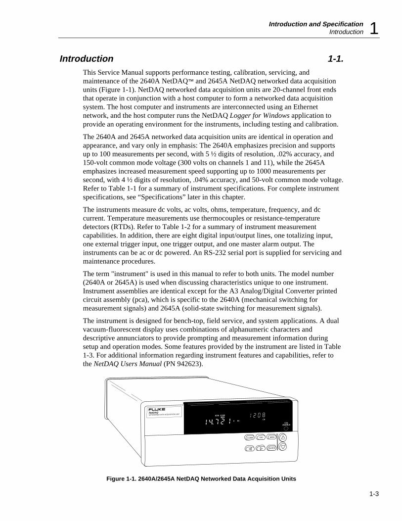
Introduction 1-1.This Service Manual supports performance testing, calibration, servicing, andmaintenance of the 2640A NetDAQ™ and 2645A NetDAQ networked data acquisitionunits (Figure 1-1). NetDAQ networked data acquisition units are 20-channel front endsthat operate in conjunction with a host computer to form a networked data acquisitionsystem. The host computer and instruments are interconnected using an Ethernetnetwork, and the host computer runs the NetDAQ Logger for Windows application toprovide an operating environment for the instruments, including testing and calibration.
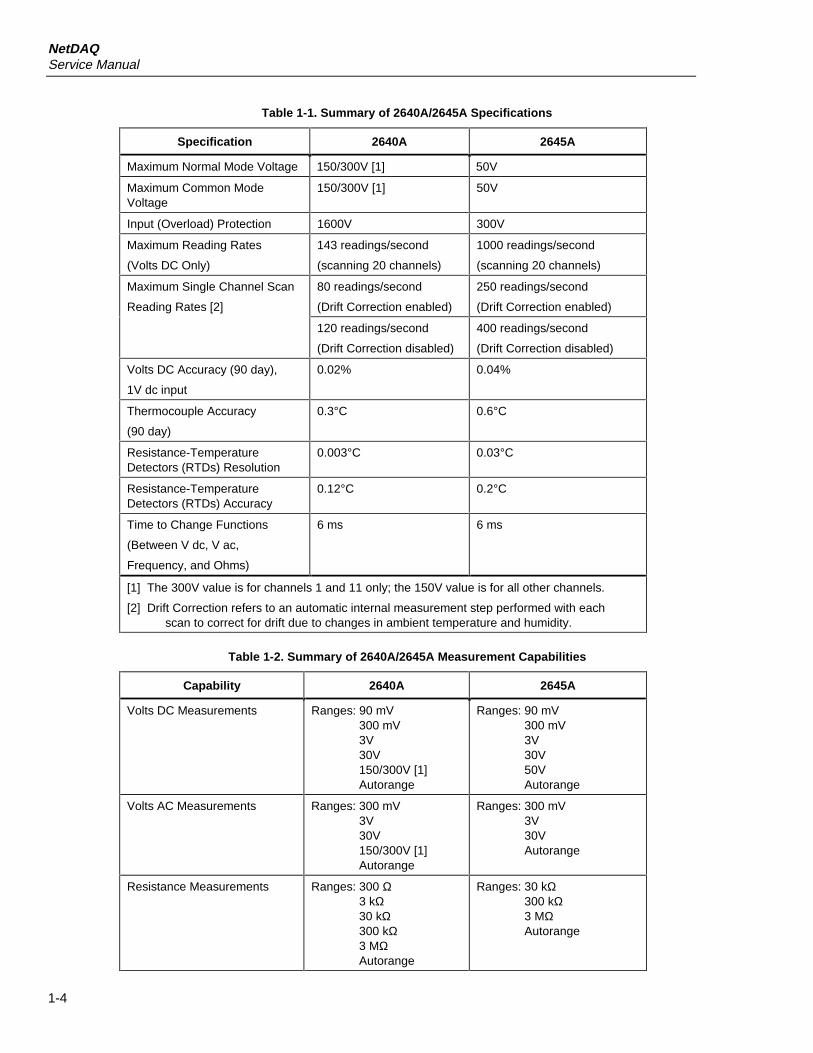
The 2640A and 2645A networked data acquisition units are identical in operation andappearance, and vary only in emphasis: The 2640A emphasizes precision and supportsup to 100 measurements per second, with 5 ½ digits of resolution, .02% accuracy, and150-volt common mode voltage (300 volts on channels 1 and 11), while the 2645Aemphasizes increased measurement speed supporting up to 1000 measurements persecond, with 4 ½ digits of resolution, .04% accuracy, and 50-volt common mode voltage.Refer to Table 1-1 for a summary of instrument specifications. For complete instrumentspecifications, see “Specifications” later in this chapter.
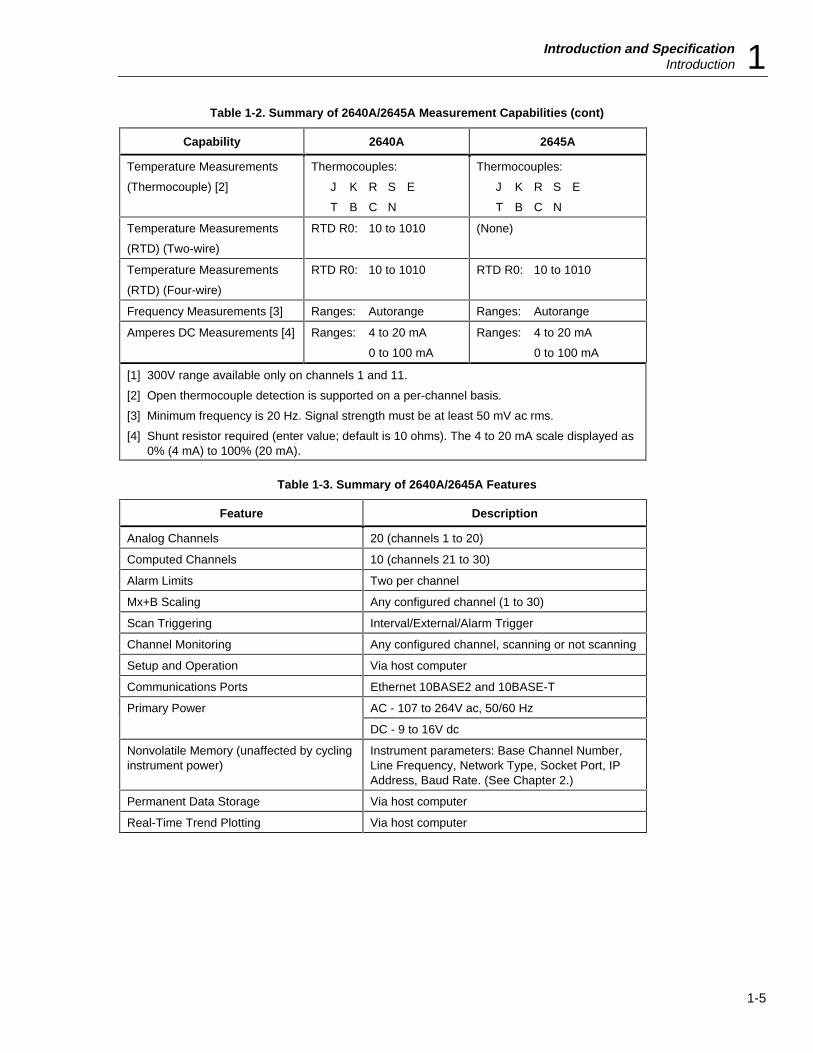
The instruments measure dc volts, ac volts, ohms, temperature, frequency, and dccurrent. Temperature measurements use thermocouples or resistance-temperaturedetectors (RTDs). Refer to Table 1-2 for a summary of instrument measurementcapabilities. In addition, there are eight digital input/output lines, one totalizing input,one external trigger input, one trigger output, and one master alarm output. Theinstruments can be ac or dc powered. An RS-232 serial port is supplied for servicing andmaintenance procedures.
The term "instrument" is used in this manual to refer to both units. The model number(2640A or 2645A) is used when discussing characteristics unique to one instrument.Instrument assemblies are identical except for the A3 Analog/Digital Converter printedcircuit assembly (pca), which is specific to the 2640A (mechanical switching formeasurement signals) and 2645A (solid-state switching for measurement signals).
The instrument is designed for bench-top, field service, and system applications. A dualvacuum-fluorescent display uses combinations of alphanumeric characters anddescriptive annunciators to provide prompting and measurement information duringsetup and operation modes. Some features provided by the instrument are listed in Table1-3. For additional information regarding instrument features and capabilities, refer tothe NetDAQ Users Manual (PN 942623).
NetDAQNETWORKED DATA ACQUISITION UNIT
COMM DIO MON
ENTER
CALENABLE
REM SCANMON
V DC
CH
Figure 1-1. 2640A/2645A NetDAQ Networked Data Acquisition Units
NetDAQService Manual
1-4
Table 1-1. Summary of 2640A/2645A Specifications
Specification 2640A 2645A
Maximum Normal Mode Voltage 150/300V [1] 50V
Maximum Common ModeVoltage
150/300V [1] 50V
Input (Overload) Protection 1600V 300V
Maximum Reading Rates
(Volts DC Only)
143 readings/second
(scanning 20 channels)
1000 readings/second
(scanning 20 channels)
Maximum Single Channel Scan
Reading Rates [2]
80 readings/second
(Drift Correction enabled)
250 readings/second
(Drift Correction enabled)
120 readings/second
(Drift Correction disabled)
400 readings/second
(Drift Correction disabled)
Volts DC Accuracy (90 day),
1V dc input
0.02% 0.04%
Thermocouple Accuracy
(90 day)
0.3°C 0.6°C
Resistance-TemperatureDetectors (RTDs) Resolution
0.003°C 0.03°C
Resistance-TemperatureDetectors (RTDs) Accuracy
0.12°C 0.2°C
Time to Change Functions
(Between V dc, V ac,
Frequency, and Ohms)
6 ms 6 ms
[1] The 300V value is for channels 1 and 11 only; the 150V value is for all other channels.
[2] Drift Correction refers to an automatic internal measurement step performed with eachscan to correct for drift due to changes in ambient temperature and humidity.
Table 1-2. Summary of 2640A/2645A Measurement Capabilities
Capability 2640A 2645A
Volts DC Measurements Ranges: 90 mV300 mV3V30V150/300V [1]Autorange
Ranges: 90 mV300 mV3V30V50VAutorange
Volts AC Measurements Ranges: 300 mV3V30V150/300V [1]Autorange
Ranges: 300 mV3V30VAutorange
Resistance Measurements Ranges: 300 Ω3 kΩ30 kΩ300 kΩ3 MΩAutorange
Ranges: 30 kΩ300 kΩ3 MΩAutorange
Introduction and SpecificationIntroduction 1
1-5
Table 1-2. Summary of 2640A/2645A Measurement Capabilities (cont)
Capability 2640A 2645A
Temperature Measurements
(Thermocouple) [2]
Thermocouples:
J K R S E
T B C N
Thermocouples:
J K R S E
T B C N
Temperature Measurements
(RTD) (Two-wire)
RTD R0: 10 to 1010 (None)
Temperature Measurements
(RTD) (Four-wire)
RTD R0: 10 to 1010 RTD R0: 10 to 1010
Frequency Measurements [3] Ranges: Autorange Ranges: Autorange
Amperes DC Measurements [4] Ranges: 4 to 20 mA
0 to 100 mA
Ranges: 4 to 20 mA
0 to 100 mA
[1] 300V range available only on channels 1 and 11.
[2] Open thermocouple detection is supported on a per-channel basis.
[3] Minimum frequency is 20 Hz. Signal strength must be at least 50 mV ac rms.
[4] Shunt resistor required (enter value; default is 10 ohms). The 4 to 20 mA scale displayed as 0% (4 mA) to 100% (20 mA).
Table 1-3. Summary of 2640A/2645A Features
Feature Description
Analog Channels 20 (channels 1 to 20)
Computed Channels 10 (channels 21 to 30)
Alarm Limits Two per channel
Mx+B Scaling Any configured channel (1 to 30)
Scan Triggering Interval/External/Alarm Trigger
Channel Monitoring Any configured channel, scanning or not scanning
Setup and Operation Via host computer
Communications Ports Ethernet 10BASE2 and 10BASE-T
Primary Power AC - 107 to 264V ac, 50/60 Hz
DC - 9 to 16V dc
Nonvolatile Memory (unaffected by cyclinginstrument power)
Instrument parameters: Base Channel Number,Line Frequency, Network Type, Socket Port, IPAddress, Baud Rate. (See Chapter 2.)
Permanent Data Storage Via host computer
Real-Time Trend Plotting Via host computer
NetDAQService Manual
1-6
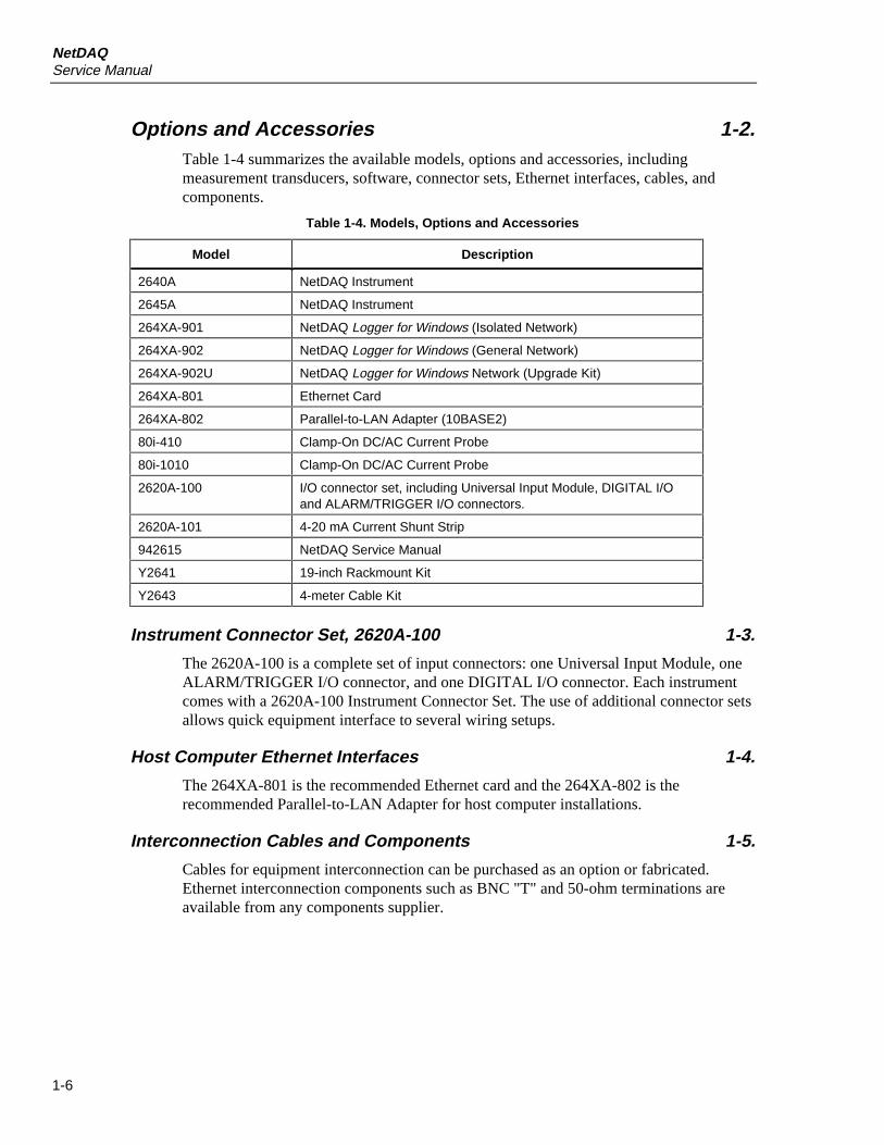
Options and Accessories 1-2.Table 1-4 summarizes the available models, options and accessories, includingmeasurement transducers, software, connector sets, Ethernet interfaces, cables, andcomponents.
Table 1-4. Models, Options and Accessories
Model Description
2640A NetDAQ Instrument
2645A NetDAQ Instrument
264XA-901 NetDAQ Logger for Windows (Isolated Network)
264XA-902 NetDAQ Logger for Windows (General Network)
264XA-902U NetDAQ Logger for Windows Network (Upgrade Kit)
264XA-801 Ethernet Card
264XA-802 Parallel-to-LAN Adapter (10BASE2)
80i-410 Clamp-On DC/AC Current Probe
80i-1010 Clamp-On DC/AC Current Probe
2620A-100 I/O connector set, including Universal Input Module, DIGITAL I/Oand ALARM/TRIGGER I/O connectors.
2620A-101 4-20 mA Current Shunt Strip
942615 NetDAQ Service Manual
Y2641 19-inch Rackmount Kit
Y2643 4-meter Cable Kit
Instrument Connector Set, 2620A-100 1-3.
The 2620A-100 is a complete set of input connectors: one Universal Input Module, oneALARM/TRIGGER I/O connector, and one DIGITAL I/O connector. Each instrumentcomes with a 2620A-100 Instrument Connector Set. The use of additional connector setsallows quick equipment interface to several wiring setups.
Host Computer Ethernet Interfaces 1-4.
The 264XA-801 is the recommended Ethernet card and the 264XA-802 is therecommended Parallel-to-LAN Adapter for host computer installations.
Interconnection Cables and Components 1-5.
Cables for equipment interconnection can be purchased as an option or fabricated.Ethernet interconnection components such as BNC "T" and 50-ohm terminations areavailable from any components supplier.
Introduction and SpecificationOperating Instructions 1
1-7
Operating Instructions 1-6.Full operating instructions are provided in the NetDAQ User Manual (PN 942623). Referto the User Manual as necessary during the maintenance and repair procedures presentedin this Service Manual.
Organization of the Service Manual 1-7.This manual focuses on performance tests, calibration procedures, and component-levelrepair of the 2640A and 2645A networked data acquisition units. To that end, manualchapters are often interdependent; effective troubleshooting may require not onlyreference to the troubleshooting procedures in Chapter 5, but also some understanding ofthe detailed Theory of Operation in Chapter 2 and some tracing of circuit operation inthe Schematic Diagrams presented in Chapter 7.
Often, scanning the table of contents yields an appropriate place to start using themanual. A comprehensive table of contents is presented at the front of the manual; localtables of contents are also presented at the beginning of each chapter for ease ofreference. If you know the topic name, the index at the end of the manual is probably agood place to start.
The following descriptions introduce the manual:
Chapter 1 - Introduction and Specifications Introduces the instrument, describing itsfeatures, options, and accessories. This chapter also discusses use of the Service Manualand the various conventions used in describing the circuitry. Finally, a complete set ofspecifications is presented.
Chapter 2 - Theory of Operation This chapter first categorizes the instrument’scircuitry into functional blocks, with a description of each block’s role in overalloperation. A detailed circuit description is then given for each block. These descriptionsexplore operation to the component level and fully support troubleshooting proceduresdefined in Chapter 5.
Chapter 3 - General Maintenance Provides maintenance information coveringhandling, cleaning, and fuse replacement. Access and reassembly procedures are alsoexplained in this chapter.
Chapter 4 - Performance Testing and Calibration This chapter provides performanceverification procedures, which relate to the specifications presented in Chapter 1. Tomaintain these specifications, a full calibration procedure is also presented.
Chapter 5 - Diagnostic Testing and Troubleshooting The troubleshooting procedurespresented in this chapter rely closely on both the Theory of Operation presented inChapter 2, the Schematic Diagrams shown in Chapter 7, and the access informationprovided in Chapter 3.
Chapter 6 - List of Replaceable Parts Includes parts lists for all standard assemblies.Information on how and where to order parts is also provided.
Chapter 7 - Schematic Diagrams Includes schematic Diagrams for all standard andoptional assemblies. A list of mnemonic definitions is also included to aid in identifyingsignal name abbreviations.
NetDAQService Manual
1-8
Conventions 1-8.Throughout the manual set, certain notational conventions are used. A summary of theseconventions follows:
• Instrument Reference The term "instrument" is used in this manual to refer to boththe 2640A NetDAQ and 2645A NetDAQ networked data acquisition units. Themodel number (2640A or 2645A) is used when discussing characteristics unique toone instrument.
• Printed Circuit Assembly The term "pca" is used to represent a printed circuitboard and its attached parts.
• Signal Logic Polarity On schematic Diagrams, a signal name followed by a "*"character is active (or asserted) low. Signals not so marked are active high.
• Circuit Nodes Individual pins or connections on a component are specified with adash (-) following the assembly and component reference designators. For example,pin 19 of U30 on assembly A1 would be A1U30-19.
• Front Panel Interface User Notation For front panel operation, XXX, anuppercase word or symbol without parentheses indicates a button to be pressed bythe user. Buttons can be pressed in four ways:
1. Press a single button to select a function or operation.
2. Press a combination of buttons, one after the other.
3. Press and hold down a button; then press another button.
4. Press multiple buttons simultaneously.
• Computer Interface User Notation For computer interface operation:
XXX An uppercase word without parentheses identifies a command by name.
<XXX> Angle brackets around all uppercase letters mean press the <XXX> key.
(xxx) A lowercase word in parentheses indicates a keyboard input.
Specifications 1-9.Specifications are divided into three sections. The first section contains the combinedspecifications that apply equally to both the 2640A and 2645A instruments. The secondsection contains specifications that apply only to the 2640A instrument. The third sectioncontains specifications that apply only to the 2645A instrument.
2640A/2645A Combined Specifications 1-10.
The following specifications apply equally to both the 2640A and 2645A instruments.The topics include:
• 2640A/2645A General Specifications
• 2640A/2645A Environmental Specifications
• 2640A/2645A Digital I/O and Totalizer Interface
Introduction and SpecificationSpecifications 1
1-9
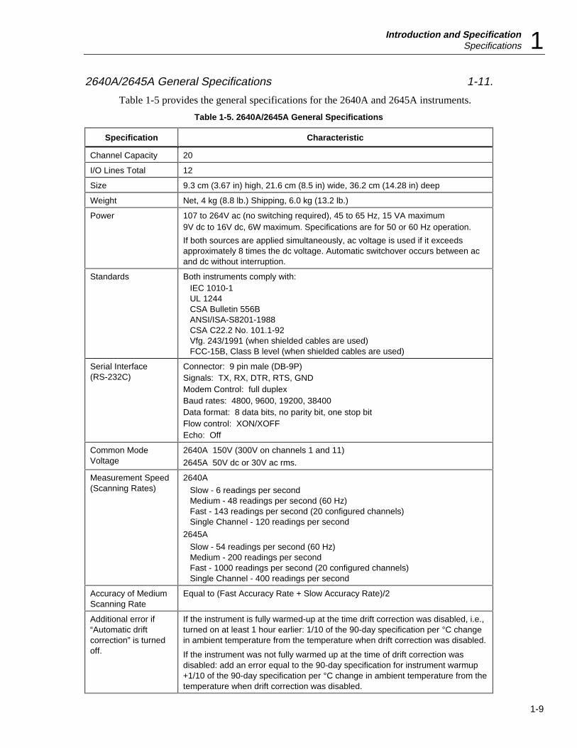
2640A/2645A General Specifications 1-11.
Table 1-5 provides the general specifications for the 2640A and 2645A instruments.
Table 1-5. 2640A/2645A General Specifications
Specification Characteristic
Channel Capacity 20
I/O Lines Total 12
Size 9.3 cm (3.67 in) high, 21.6 cm (8.5 in) wide, 36.2 cm (14.28 in) deep
Weight Net, 4 kg (8.8 lb.) Shipping, 6.0 kg (13.2 lb.)
Power 107 to 264V ac (no switching required), 45 to 65 Hz, 15 VA maximum9V dc to 16V dc, 6W maximum. Specifications are for 50 or 60 Hz operation.
If both sources are applied simultaneously, ac voltage is used if it exceedsapproximately 8 times the dc voltage. Automatic switchover occurs between acand dc without interruption.
Standards Both instruments comply with:IEC 1010-1UL 1244CSA Bulletin 556BANSI/ISA-S8201-1988CSA C22.2 No. 101.1-92Vfg. 243/1991 (when shielded cables are used)FCC-15B, Class B level (when shielded cables are used)
Serial Interface(RS-232C)
Connector: 9 pin male (DB-9P)Signals: TX, RX, DTR, RTS, GNDModem Control: full duplexBaud rates: 4800, 9600, 19200, 38400Data format: 8 data bits, no parity bit, one stop bitFlow control: XON/XOFFEcho: Off
Common ModeVoltage
2640A 150V (300V on channels 1 and 11)
2645A 50V dc or 30V ac rms.
Measurement Speed(Scanning Rates)
2640A
Slow - 6 readings per secondMedium - 48 readings per second (60 Hz)Fast - 143 readings per second (20 configured channels)Single Channel - 120 readings per second
2645A
Slow - 54 readings per second (60 Hz)Medium - 200 readings per secondFast - 1000 readings per second (20 configured channels)Single Channel - 400 readings per second
Accuracy of MediumScanning Rate
Equal to (Fast Accuracy Rate + Slow Accuracy Rate)/2
Additional error if“Automatic driftcorrection” is turnedoff.
If the instrument is fully warmed-up at the time drift correction was disabled, i.e.,turned on at least 1 hour earlier: 1/10 of the 90-day specification per °C changein ambient temperature from the temperature when drift correction was disabled.
If the instrument was not fully warmed up at the time of drift correction wasdisabled: add an error equal to the 90-day specification for instrument warmup+1/10 of the 90-day specification per °C change in ambient temperature from thetemperature when drift correction was disabled.
NetDAQService Manual
1-10
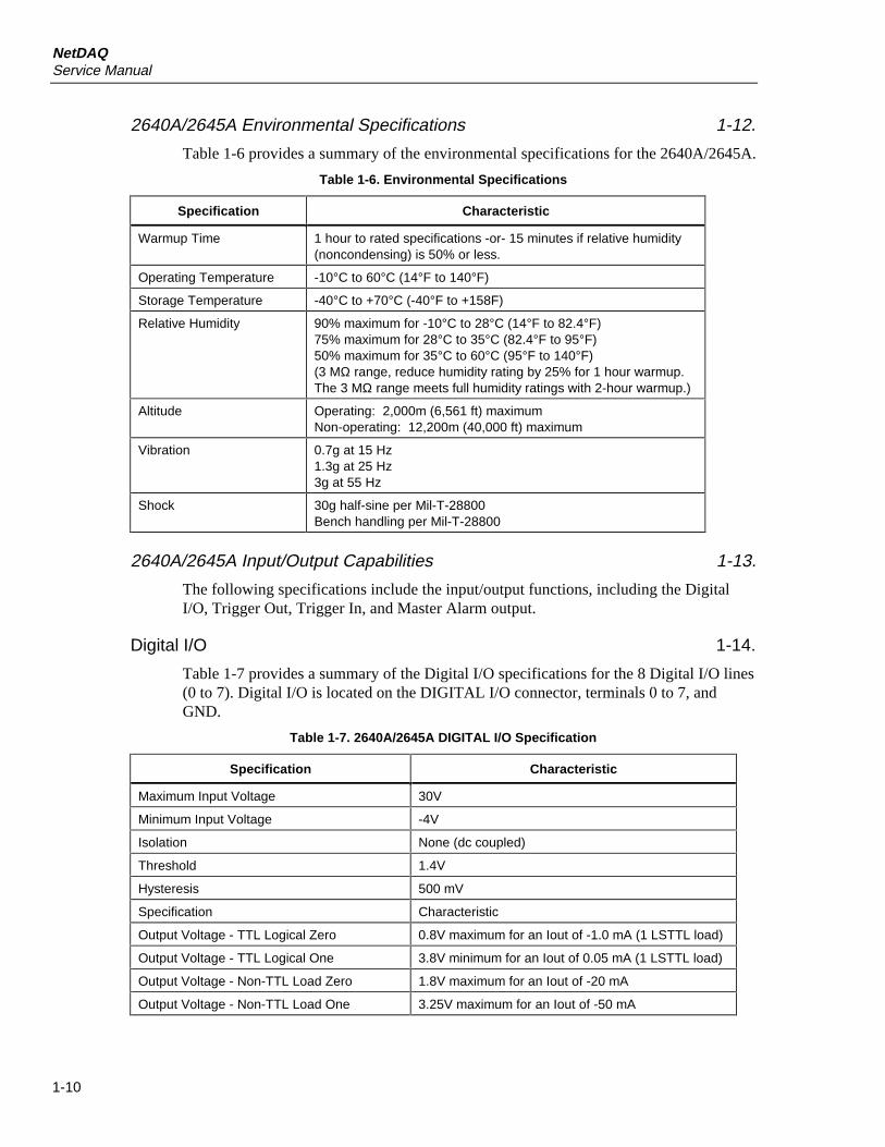
2640A/2645A Environmental Specifications 1-12.
Table 1-6 provides a summary of the environmental specifications for the 2640A/2645A.
Table 1-6. Environmental Specifications
Specification Characteristic
Warmup Time 1 hour to rated specifications -or- 15 minutes if relative humidity(noncondensing) is 50% or less.
Operating Temperature -10°C to 60°C (14°F to 140°F)
Storage Temperature -40°C to +70°C (-40°F to +158F)
Relative Humidity 90% maximum for -10°C to 28°C (14°F to 82.4°F)75% maximum for 28°C to 35°C (82.4°F to 95°F)50% maximum for 35°C to 60°C (95°F to 140°F)(3 MΩ range, reduce humidity rating by 25% for 1 hour warmup.The 3 MΩ range meets full humidity ratings with 2-hour warmup.)
Altitude Operating: 2,000m (6,561 ft) maximumNon-operating: 12,200m (40,000 ft) maximum
Vibration 0.7g at 15 Hz1.3g at 25 Hz3g at 55 Hz
Shock 30g half-sine per Mil-T-28800Bench handling per Mil-T-28800
2640A/2645A Input/Output Capabilities 1-13.
The following specifications include the input/output functions, including the DigitalI/O, Trigger Out, Trigger In, and Master Alarm output.
Digital I/O 1-14.
Table 1-7 provides a summary of the Digital I/O specifications for the 8 Digital I/O lines(0 to 7). Digital I/O is located on the DIGITAL I/O connector, terminals 0 to 7, andGND.
Table 1-7. 2640A/2645A DIGITAL I/O Specification
Specification Characteristic
Maximum Input Voltage 30V
Minimum Input Voltage -4V
Isolation None (dc coupled)
Threshold 1.4V
Hysteresis 500 mV
Specification Characteristic
Output Voltage - TTL Logical Zero 0.8V maximum for an Iout of -1.0 mA (1 LSTTL load)
Output Voltage - TTL Logical One 3.8V minimum for an Iout of 0.05 mA (1 LSTTL load)
Output Voltage - Non-TTL Load Zero 1.8V maximum for an Iout of -20 mA
Output Voltage - Non-TTL Load One 3.25V maximum for an Iout of -50 mA
Introduction and SpecificationSpecifications 1
1-11
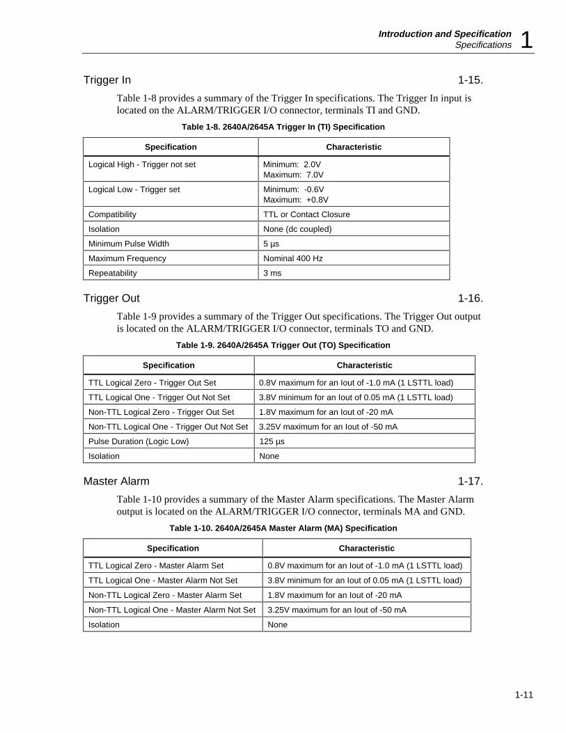
Trigger In 1-15.
Table 1-8 provides a summary of the Trigger In specifications. The Trigger In input islocated on the ALARM/TRIGGER I/O connector, terminals TI and GND.
Table 1-8. 2640A/2645A Trigger In (TI) Specification
Specification Characteristic
Logical High - Trigger not set Minimum: 2.0VMaximum: 7.0V
Logical Low - Trigger set Minimum: -0.6VMaximum: +0.8V
Compatibility TTL or Contact Closure
Isolation None (dc coupled)
Minimum Pulse Width 5 µs
Maximum Frequency Nominal 400 Hz
Repeatability 3 ms
Trigger Out 1-16.
Table 1-9 provides a summary of the Trigger Out specifications. The Trigger Out outputis located on the ALARM/TRIGGER I/O connector, terminals TO and GND.
Table 1-9. 2640A/2645A Trigger Out (TO) Specification
Specification Characteristic
TTL Logical Zero - Trigger Out Set 0.8V maximum for an Iout of -1.0 mA (1 LSTTL load)
TTL Logical One - Trigger Out Not Set 3.8V minimum for an Iout of 0.05 mA (1 LSTTL load)
Non-TTL Logical Zero - Trigger Out Set 1.8V maximum for an Iout of -20 mA
Non-TTL Logical One - Trigger Out Not Set 3.25V maximum for an Iout of -50 mA
Pulse Duration (Logic Low) 125 µs
Isolation None
Master Alarm 1-17.
Table 1-10 provides a summary of the Master Alarm specifications. The Master Alarmoutput is located on the ALARM/TRIGGER I/O connector, terminals MA and GND.
Table 1-10. 2640A/2645A Master Alarm (MA) Specification
Specification Characteristic
TTL Logical Zero - Master Alarm Set 0.8V maximum for an Iout of -1.0 mA (1 LSTTL load)
TTL Logical One - Master Alarm Not Set 3.8V minimum for an Iout of 0.05 mA (1 LSTTL load)
Non-TTL Logical Zero - Master Alarm Set 1.8V maximum for an Iout of -20 mA
Non-TTL Logical One - Master Alarm Not Set 3.25V maximum for an Iout of -50 mA
Isolation None
NetDAQService Manual
1-12
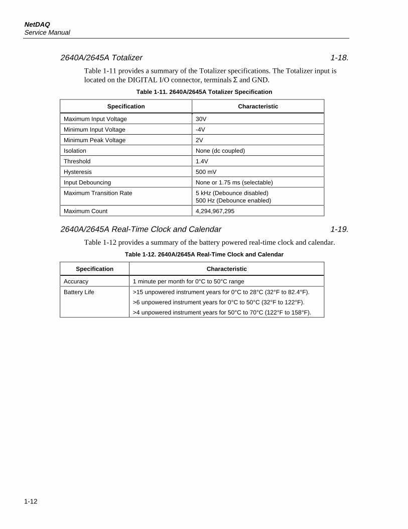
2640A/2645A Totalizer 1-18.
Table 1-11 provides a summary of the Totalizer specifications. The Totalizer input islocated on the DIGITAL I/O connector, terminals Σ and GND.
Table 1-11. 2640A/2645A Totalizer Specification
Specification Characteristic
Maximum Input Voltage 30V
Minimum Input Voltage -4V
Minimum Peak Voltage 2V
Isolation None (dc coupled)
Threshold 1.4V
Hysteresis 500 mV
Input Debouncing None or 1.75 ms (selectable)
Maximum Transition Rate 5 kHz (Debounce disabled)500 Hz (Debounce enabled)
Maximum Count 4,294,967,295
2640A/2645A Real-Time Clock and Calendar 1-19.
Table 1-12 provides a summary of the battery powered real-time clock and calendar.
Table 1-12. 2640A/2645A Real-Time Clock and Calendar
Specification Characteristic
Accuracy 1 minute per month for 0°C to 50°C range
Battery Life >15 unpowered instrument years for 0°C to 28°C (32°F to 82.4°F).
>6 unpowered instrument years for 0°C to 50°C (32°F to 122°F).
>4 unpowered instrument years for 50°C to 70°C (122°F to 158°F).
Introduction and SpecificationSpecifications 1
1-13
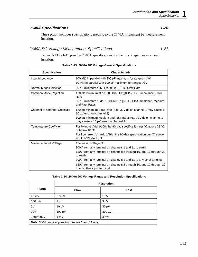
2640A Specifications 1-20.
This section includes specifications specific to the 2640A instrument by measurementfunction.
2640A DC Voltage Measurement Specifications 1-21.
Tables 1-13 to 1-15 provide 2640A specifications for the dc voltage measurementfunction.
Table 1-13. 2640A DC Voltage General Specifications
Specification Characteristic
Input Impedance 100 MΩ in parallel with 300 pF maximum for ranges <=3V
10 MΩ in parallel with 100 pF maximum for ranges >3V
Normal Mode Rejection 50 dB minimum at 50 Hz/60 Hz +0.1%, Slow Rate
Common Mode Rejection 120 dB minimum at dc, 50 Hz/60 Hz +0.1%, 1 kΩ imbalance, Slow Rate
80 dB minimum at dc, 50 Hz/60 Hz +0.1%, 1 kΩ imbalance, Medium and Fast Rates
Channel-to-Channel Crosstalk 120 dB minimum Slow Rate (e.g., 30V dc on channel 1 may cause a30 µV error on channel 2)
100 dB minimum Medium and Fast Rates (e.g., 1V dc on channel 1may cause a 10 µV error on channel 2)
Temperature Coefficient For % input: Add 1/10th the 90-day specification per °C above 28 °Cor below 18 °CFor floor error (V): Add 1/20th the 90-day specification per °C above28 °C or below 18 °C
Maximum Input Voltage The lesser voltage of:
300V from any terminal on channels 1 and 11 to earth;
150V from any terminal on channels 2 through 10, and 12 through 20to earth;
300V from any terminal on channels 1 and 11 to any other terminal;
150V from any terminal on channels 2 through 10, and 12 through 20to any other input terminal
Table 1-14. 2640A DC Voltage Range and Resolution Specifications
Resolution
Range Slow Fast
90 mV 0.3 µV 1 µV
300 mV 1 µV 3 µV
3V 10 µV 30 µV
30V 100 µV 300 µV
150V/300V 1 mV 3 mV
Note 300V range applies to channels 1 and 11 only.
NetDAQService Manual
1-14
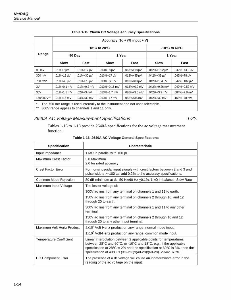
Table 1-15. 2640A DC Voltage Accuracy Specifications
Accuracy, 3σ + (% input + V)
18°C to 28°C -10°C to 60°C
Range 90 Day 1 Year 1 Year
Slow Fast Slow Fast Slow Fast
90 mV .01%+7 µV .01%+17 µV .013%+8 µV .013%+18 µV .042%+18.2 µV .042%+44.2 µV
300 mV .01%+15 µV .01%+30 µV .013%+17 µV .013%+35 µV .042%+39 µV .042%+78 µV
750 mV* .01%+40 µV .01%+70 µV .013%+50 µV .013%+80 µV .042%+104 µV .042%+182 µV
3V .01%+0.1 mV .01%+0.2 mV .013%+0.15 mV .013%+0.2 mV .042%+0.26 mV .042%+0.52 mV
30V .01%+1.5 mV .02%+3 mV .013%+1.7 mV .026%+3.5 mV .042%+3.9 mV .084%+7.8 mV
150/300V** .01%+15 mV .04%+30 mV .013%+17 mV .052%+35 mV .042%+39 mV .168%+78 mV
* The 750 mV range is used internally to the instrument and not user selectable.** 300V range applies to channels 1 and 11 only.
2640A AC Voltage Measurement Specifications 1-22.
Tables 1-16 to 1-18 provide 2640A specifications for the ac voltage measurementfunction.
Table 1-16. 2640A AC Voltage General Specifications
Specification Characteristic
Input Impedance 1 MΩ in parallel with 100 pF
Maximum Crest Factor 3.0 Maximum2.0 for rated accuracy
Crest Factor Error For nonsinusoidal input signals with crest factors between 2 and 3 andpulse widths >=100 µs, add 0.2% to the accuracy specifications.
Common Mode Rejection 80 dB minimum at dc, 50 Hz/60 Hz +0.1%, 1 kΩ imbalance, Slow Rate
Maximum Input Voltage The lesser voltage of:
300V ac rms from any terminal on channels 1 and 11 to earth.
150V ac rms from any terminal on channels 2 through 10, and 12through 20 to earth.
300V ac rms from any terminal on channels 1 and 11 to any otherterminal.
150V ac rms from any terminal on channels 2 through 10 and 12through 20 to any other input terminal.
Maximum Volt-Hertz Product 2x10⁶ Volt-Hertz product on any range, normal mode input.
1x10⁶ Volt-Hertz product on any range, common mode input.
Temperature Coefficient Linear interpolation between 2 applicable points for temperaturesbetween 28°C and 60°C, or -10°C and 18°C, e.g., if the applicablespecification at 28°C is 2% and the specification at 60°C is 3%, then thespecification at 40°C is (3%-2%)x(40-28)/(60-28)+2%=2.375%.
DC Component Error The presence of a dc voltage will cause an indeterminate error in thereading of the ac voltage on the input.
Introduction and SpecificationSpecifications 1
1-15
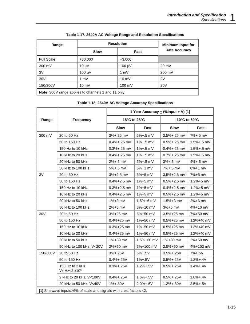
Table 1-17. 2640A AC Voltage Range and Resolution Specifications
Range Resolution Minimum Input for
Slow Fast Rate Accuracy
Full Scale +30,000 +3,000
300 mV 10 µV 100 µV 20 mV
3V 100 µV 1 mV 200 mV
30V 1 mV 10 mV 2V
150/300V 10 mV 100 mV 20V
Note 300V range applies to channels 1 and 11 only.
Table 1-18. 2640A AC Voltage Accuracy Specifications
1 Year Accuracy + (%input + V) [1]
Range Frequency 18°C to 28°C -10°C to 60°C
Slow Fast Slow Fast
300 mV 20 to 50 Hz 3%+.25 mV 6%+.5 mV 3.5%+.25 mV 7%+.5 mV
50 to 150 Hz 0.4%+.25 mV 1%+.5 mV 0.5%+.25 mV 1.5%+.5 mV
150 Hz to 10 kHz 0.3%+.25 mV 1%+.5 mV 0.4%+.25 mV 1.5%+.5 mV
10 kHz to 20 kHz 0.4%+.25 mV 1%+.5 mV 0.7%+.25 mV 1.5%+.5 mV
20 kHz to 50 kHz 2%+.3 mV 3%+.5 mV 3%+.3 mV 4%+.5 mV
50 kHz to 100 kHz 5%+.5 mV 5%+1 mV 7%+.5 mV 8%+1 mV
3V 20 to 50 Hz 3%+2.5 mV 6%+5 mV 3.5%+2.5 mV 7%+5 mV
50 to 150 Hz 0.4%+2.5 mV 1%+5 mV 0.5%+2.5 mV 1.2%+5 mV
150 Hz to 10 kHz 0.3%+2.5 mV 1%+5 mV 0.4%+2.5 mV 1.2%+5 mV
10 kHz to 20 kHz 0.4%+2.5 mV 1%+5 mV 0.5%+2.5 mV 1.2%+5 mV
20 kHz to 50 kHz 1%+3 mV 1.5%+6 mV 1.5%+3 mV 2%+6 mV
50 kHz to 100 kHz 2%+5 mV 3%+10 mV 3%+5 mV 4%+10 mV
30V 20 to 50 Hz 3%+25 mV 6%+50 mV 3.5%+25 mV 7%+50 mV
50 to 150 Hz 0.4%+25 mV 1%+50 mV 0.5%+25 mV 1.2%+40 mV
150 Hz to 10 kHz 0.3%+25 mV 1%+50 mV 0.5%+25 mV 1.2%+40 mV
10 kHz to 20 kHz 0.4%+25 mV 1%+50 mV 0.5%+25 mV 1.2%+40 mV
20 kHz to 50 kHz 1%+30 mV 1.5%+60 mV 1%+30 mV 2%+50 mV
50 kHz to 100 kHz, V<20V 2%+50 mV 3%+100 mV 2.5%+50 mV 4%+100 mV
150/300V 20 to 50 Hz 3%+.25V 6%+.5V 3.5%+.25V 7%+.5V
50 to 150 Hz 0.4%+.25V 1%+.5V 0.5%+.25V 1.2%+.4V
150 Hz to 2 kHzVx Hz<2 x10⁶
0.3%+.25V 1.2%+.5V 0.5%+.25V 1.4%+.4V
2 kHz to 20 kHz, V<100V 0.4%+.25V 1.6%+.5V 0.5%+.25V 1.8%+.4V
20 kHz to 50 kHz, V<40V 1%+.30V 2.0%+.6V 1.2%+.30V 2.5%+.5V
[1] Sinewave inputs>6% of scale and signals with crest factors <2.
NetDAQService Manual
1-16
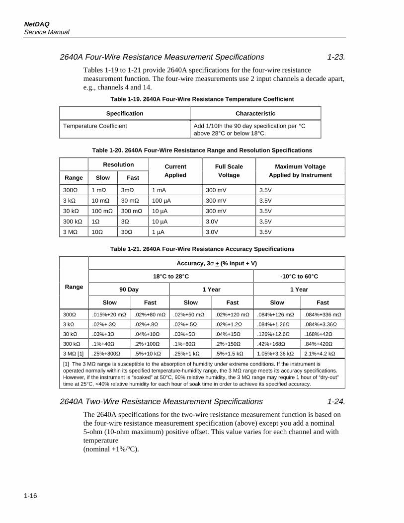
2640A Four-Wire Resistance Measurement Specifications 1-23.
Tables 1-19 to 1-21 provide 2640A specifications for the four-wire resistancemeasurement function. The four-wire measurements use 2 input channels a decade apart,e.g., channels 4 and 14.
Table 1-19. 2640A Four-Wire Resistance Temperature Coefficient
Specification Characteristic
Temperature Coefficient Add 1/10th the 90 day specification per °Cabove 28°C or below 18°C.
Table 1-20. 2640A Four-Wire Resistance Range and Resolution Specifications
Resolution Current Full Scale Maximum Voltage
Range Slow Fast Applied Voltage Applied by Instrument
300Ω 1 mΩ 3mΩ 1 mA 300 mV 3.5V
3 kΩ 10 mΩ 30 mΩ 100 µA 300 mV 3.5V
30 kΩ 100 mΩ 300 mΩ 10 µA 300 mV 3.5V
300 kΩ 1Ω 3Ω 10 µA 3.0V 3.5V
3 MΩ 10Ω 30Ω 1 µA 3.0V 3.5V
Table 1-21. 2640A Four-Wire Resistance Accuracy Specifications
Accuracy, 3σ + (% input + V)
18°C to 28°C -10°C to 60°C
Range 90 Day 1 Year 1 Year
Slow Fast Slow Fast Slow Fast
300Ω .015%+20 mΩ .02%+80 mΩ .02%+50 mΩ .02%+120 mΩ .084%+126 mΩ .084%+336 mΩ
3 kΩ .02%+.3Ω .02%+.8Ω .02%+.5Ω .02%+1.2Ω .084%+1.26Ω .084%+3.36Ω
30 kΩ .03%+3Ω .04%+10Ω .03%+5Ω .04%+15Ω .126%+12.6Ω .168%+42Ω
300 kΩ .1%+40Ω .2%+100Ω .1%+60Ω .2%+150Ω .42%+168Ω .84%+420Ω
3 MΩ [1] .25%+800Ω .5%+10 kΩ .25%+1 kΩ .5%+1.5 kΩ 1.05%+3.36 kΩ 2.1%+4.2 kΩ
[1] The 3 MΩ range is susceptible to the absorption of humidity under extreme conditions. If the instrument isoperated normally within its specified temperature-humidity range, the 3 MΩ range meets its accuracy specifications.However, if the instrument is “soaked” at 50°C, 90% relative humidity, the 3 MΩ range may require 1 hour of “dry-out”time at 25°C, <40% relative humidity for each hour of soak time in order to achieve its specified accuracy.
2640A Two-Wire Resistance Measurement Specifications 1-24.
The 2640A specifications for the two-wire resistance measurement function is based onthe four-wire resistance measurement specification (above) except you add a nominal5-ohm (10-ohm maximum) positive offset. This value varies for each channel and withtemperature(nominal +1%/ºC).
Introduction and SpecificationSpecifications 1
1-17
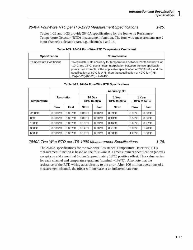
2640A Four-Wire RTD per ITS-1990 Measurement Specifications 1-25.
Tables 1-22 and 1-23 provide 2640A specifications for the four-wire Resistance-Temperature Detector (RTD) measurement function. The four-wire measurements use 2input channels a decade apart, e.g., channels 4 and 14.
Table 1-22. 2640A Four-Wire RTD Temperature Coefficient
Specification Characteristic
Temperature Coefficient To calculate RTD accuracy for temperatures between 28°C and 60°C, or-10°C and 18°C, use a linear interpolation between the two applicablepoints. For example, if the applicable specification at 28°C is 0.2 and thespecification at 60°C is 0.75, then the specification at 40°C is =(.75-.2)x(40-28)/(60-28)+.2=0.406.
Table 1-23. 2640A Four-Wire RTD Specifications
Accuracy, 3σ
TemperatureResolution 90 Day
18°C to 28°C1 Year
18°C to 28°C1 Year
-10°C to 60°C
Slow Fast Slow Fast Slow Slow Fast
-200°C 0.003°C 0.007°C 0.06°C 0.16°C 0.09°C 0.33°C 0.63°C
0°C 0.003°C 0.007°C 0.09°C 0.20°C 0.13°C 0.53°C 0.86°C
100°C 0.003°C 0.007°C 0.10°C 0.23°C 0.16°C 0.63°C 0.97°C
300°C 0.003°C 0.007°C 0.14°C 0.30°C 0.21°C 0.83°C 1.20°C
600°C 0.003°C 0.007°C 0.19°C 0.53°C 0.30°C 1.20°C 1.60°C
2640A Two-Wire RTD per ITS-1990 Measurement Specifications 1-26.
The 2640A specifications for the two-wire Resistance-Temperature Detector (RTD)measurement function is based on the four-wire RTD measurement specification (above)except you add a nominal 5-ohm (approximately 13°C) positive offset. This value variesfor each channel and temperature gradient (nominal +1%/ºC). Also note that theresistance of the RTD wiring adds directly to the error. After 100 million operations of ameasurement channel, the offset will increase at an indeterminate rate.
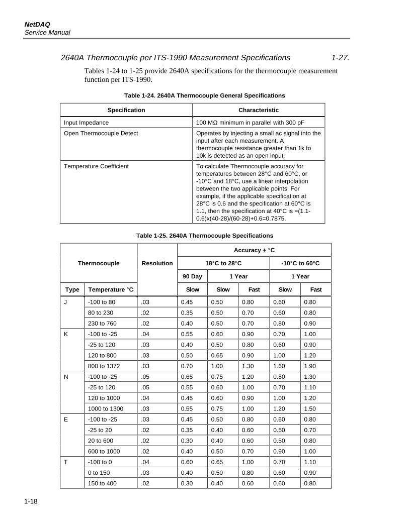
NetDAQService Manual
1-18
2640A Thermocouple per ITS-1990 Measurement Specifications 1-27.
Tables 1-24 to 1-25 provide 2640A specifications for the thermocouple measurementfunction per ITS-1990.
Table 1-24. 2640A Thermocouple General Specifications
Specification Characteristic
Input Impedance 100 MΩ minimum in parallel with 300 pF
Open Thermocouple Detect Operates by injecting a small ac signal into theinput after each measurement. Athermocouple resistance greater than 1k to10k is detected as an open input.
Temperature Coefficient To calculate Thermocouple accuracy fortemperatures between 28°C and 60°C, or-10°C and 18°C, use a linear interpolationbetween the two applicable points. Forexample, if the applicable specification at28°C is 0.6 and the specification at 60°C is1.1, then the specification at 40°C is =(1.1-0.6)x(40-28)/(60-28)+0.6=0.7875.
Table 1-25. 2640A Thermocouple Specifications
Accuracy + °C
Thermocouple Resolution 18°C to 28°C -10°C to 60°C
90 Day 1 Year 1 Year
Type Temperature °C Slow Slow Fast Slow Fast
J -100 to 80 .03 0.45 0.50 0.80 0.60 0.80
80 to 230 .02 0.35 0.50 0.70 0.60 0.80
230 to 760 .02 0.40 0.50 0.70 0.80 0.90
K -100 to -25 .04 0.55 0.60 0.90 0.70 1.00
-25 to 120 .03 0.40 0.50 0.80 0.60 0.90
120 to 800 .03 0.50 0.65 0.90 1.00 1.20
800 to 1372 .03 0.70 1.00 1.30 1.60 1.90
N -100 to -25 .05 0.65 0.75 1.20 0.80 1.30
-25 to 120 .05 0.55 0.60 1.00 0.70 1.10
120 to 1000 .04 0.45 0.60 0.90 1.00 1.20
1000 to 1300 .03 0.55 0.75 1.00 1.20 1.50
E -100 to -25 .03 0.45 0.50 0.80 0.60 0.80
-25 to 20 .02 0.35 0.40 0.60 0.50 0.70
20 to 600 .02 0.30 0.40 0.60 0.50 0.80
600 to 1000 .02 0.40 0.50 0.70 0.90 1.00
T -100 to 0 .04 0.60 0.65 1.00 0.70 1.10
0 to 150 .03 0.40 0.50 0.80 0.60 0.90
150 to 400 .02 0.30 0.40 0.60 0.60 0.80
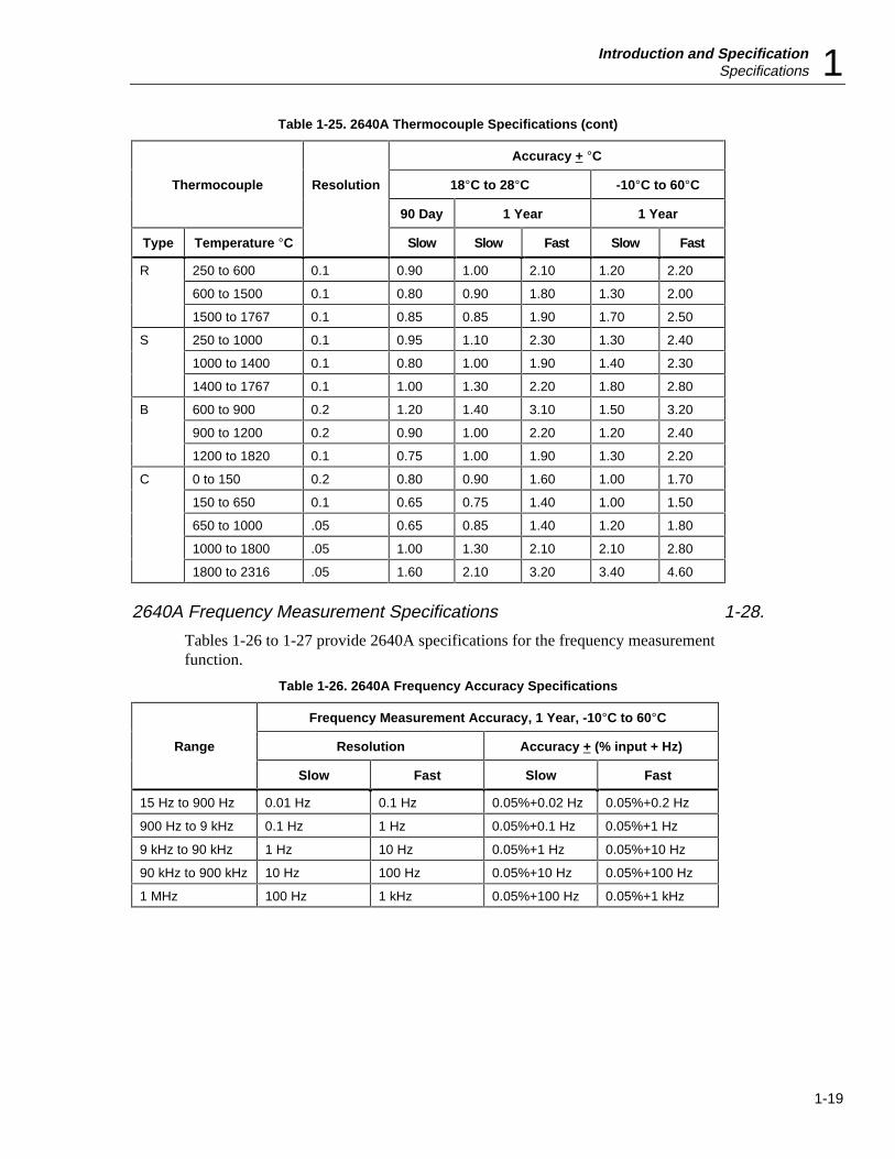
Introduction and SpecificationSpecifications 1
1-19
Table 1-25. 2640A Thermocouple Specifications (cont)
Accuracy + °C
Thermocouple Resolution 18°C to 28°C -10°C to 60°C
90 Day 1 Year 1 Year
Type Temperature °C Slow Slow Fast Slow Fast
R 250 to 600 0.1 0.90 1.00 2.10 1.20 2.20
600 to 1500 0.1 0.80 0.90 1.80 1.30 2.00
1500 to 1767 0.1 0.85 0.85 1.90 1.70 2.50
S 250 to 1000 0.1 0.95 1.10 2.30 1.30 2.40
1000 to 1400 0.1 0.80 1.00 1.90 1.40 2.30
1400 to 1767 0.1 1.00 1.30 2.20 1.80 2.80
B 600 to 900 0.2 1.20 1.40 3.10 1.50 3.20
900 to 1200 0.2 0.90 1.00 2.20 1.20 2.40
1200 to 1820 0.1 0.75 1.00 1.90 1.30 2.20
C 0 to 150 0.2 0.80 0.90 1.60 1.00 1.70
150 to 650 0.1 0.65 0.75 1.40 1.00 1.50
650 to 1000 .05 0.65 0.85 1.40 1.20 1.80
1000 to 1800 .05 1.00 1.30 2.10 2.10 2.80
1800 to 2316 .05 1.60 2.10 3.20 3.40 4.60
2640A Frequency Measurement Specifications 1-28.
Tables 1-26 to 1-27 provide 2640A specifications for the frequency measurementfunction.
Table 1-26. 2640A Frequency Accuracy Specifications
Frequency Measurement Accuracy, 1 Year, -10°C to 60°C
Range Resolution Accuracy + (% input + Hz)
Slow Fast Slow Fast
15 Hz to 900 Hz 0.01 Hz 0.1 Hz 0.05%+0.02 Hz 0.05%+0.2 Hz
900 Hz to 9 kHz 0.1 Hz 1 Hz 0.05%+0.1 Hz 0.05%+1 Hz
9 kHz to 90 kHz 1 Hz 10 Hz 0.05%+1 Hz 0.05%+10 Hz
90 kHz to 900 kHz 10 Hz 100 Hz 0.05%+10 Hz 0.05%+100 Hz
1 MHz 100 Hz 1 kHz 0.05%+100 Hz 0.05%+1 kHz
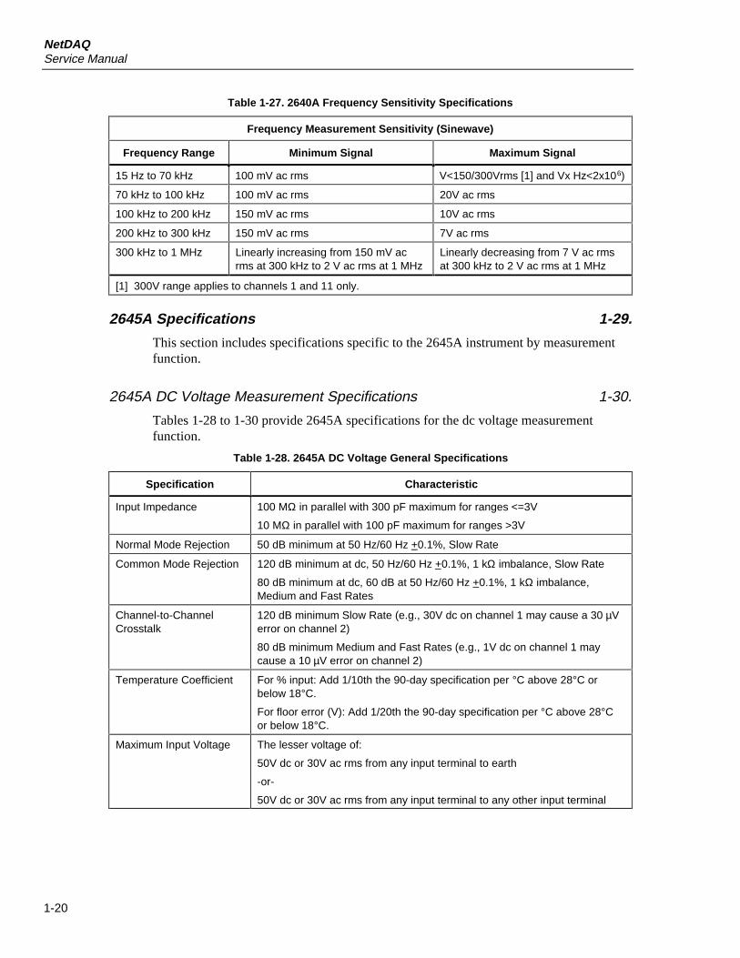
NetDAQService Manual
1-20
Table 1-27. 2640A Frequency Sensitivity Specifications
Frequency Measurement Sensitivity (Sinewave)
Frequency Range Minimum Signal Maximum Signal
15 Hz to 70 kHz 100 mV ac rms V<150/300Vrms [1] and Vx Hz<2x10⁶)
70 kHz to 100 kHz 100 mV ac rms 20V ac rms
100 kHz to 200 kHz 150 mV ac rms 10V ac rms
200 kHz to 300 kHz 150 mV ac rms 7V ac rms
300 kHz to 1 MHz Linearly increasing from 150 mV acrms at 300 kHz to 2 V ac rms at 1 MHz
Linearly decreasing from 7 V ac rmsat 300 kHz to 2 V ac rms at 1 MHz
[1] 300V range applies to channels 1 and 11 only.
2645A Specifications 1-29.
This section includes specifications specific to the 2645A instrument by measurementfunction.
2645A DC Voltage Measurement Specifications 1-30.
Tables 1-28 to 1-30 provide 2645A specifications for the dc voltage measurementfunction.
Table 1-28. 2645A DC Voltage General Specifications
Specification Characteristic
Input Impedance 100 MΩ in parallel with 300 pF maximum for ranges <=3V
10 MΩ in parallel with 100 pF maximum for ranges >3V
Normal Mode Rejection 50 dB minimum at 50 Hz/60 Hz +0.1%, Slow Rate
Common Mode Rejection 120 dB minimum at dc, 50 Hz/60 Hz +0.1%, 1 kΩ imbalance, Slow Rate
80 dB minimum at dc, 60 dB at 50 Hz/60 Hz +0.1%, 1 kΩ imbalance, Medium and Fast Rates
Channel-to-ChannelCrosstalk
120 dB minimum Slow Rate (e.g., 30V dc on channel 1 may cause a 30 µVerror on channel 2)
80 dB minimum Medium and Fast Rates (e.g., 1V dc on channel 1 maycause a 10 µV error on channel 2)
Temperature Coefficient For % input: Add 1/10th the 90-day specification per °C above 28°C orbelow 18°C.
For floor error (V): Add 1/20th the 90-day specification per °C above 28°Cor below 18°C.
Maximum Input Voltage The lesser voltage of:
50V dc or 30V ac rms from any input terminal to earth
-or-
50V dc or 30V ac rms from any input terminal to any other input terminal
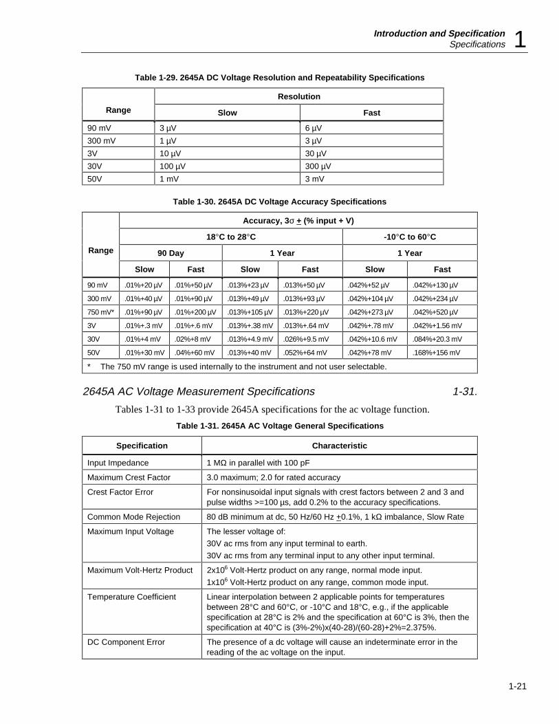
Introduction and SpecificationSpecifications 1
1-21
Table 1-29. 2645A DC Voltage Resolution and Repeatability Specifications
Resolution
Range Slow Fast
90 mV 3 µV 6 µV
300 mV 1 µV 3 µV
3V 10 µV 30 µV
30V 100 µV 300 µV
50V 1 mV 3 mV
Table 1-30. 2645A DC Voltage Accuracy Specifications
Accuracy, 3σ + (% input + V)
18°C to 28°C -10°C to 60°C
Range 90 Day 1 Year 1 Year
Slow Fast Slow Fast Slow Fast
90 mV .01%+20 µV .01%+50 µV .013%+23 µV .013%+50 µV .042%+52 µV .042%+130 µV
300 mV .01%+40 µV .01%+90 µV .013%+49 µV .013%+93 µV .042%+104 µV .042%+234 µV
750 mV* .01%+90 µV .01%+200 µV .013%+105 µV .013%+220 µV .042%+273 µV .042%+520 µV
3V .01%+.3 mV .01%+.6 mV .013%+.38 mV .013%+.64 mV .042%+.78 mV .042%+1.56 mV
30V .01%+4 mV .02%+8 mV .013%+4.9 mV .026%+9.5 mV .042%+10.6 mV .084%+20.3 mV
50V .01%+30 mV .04%+60 mV .013%+40 mV .052%+64 mV .042%+78 mV .168%+156 mV
* The 750 mV range is used internally to the instrument and not user selectable.
2645A AC Voltage Measurement Specifications 1-31.
Tables 1-31 to 1-33 provide 2645A specifications for the ac voltage function.
Table 1-31. 2645A AC Voltage General Specifications
Specification Characteristic
Input Impedance 1 MΩ in parallel with 100 pF
Maximum Crest Factor 3.0 maximum; 2.0 for rated accuracy
Crest Factor Error For nonsinusoidal input signals with crest factors between 2 and 3 andpulse widths >=100 µs, add 0.2% to the accuracy specifications.
Common Mode Rejection 80 dB minimum at dc, 50 Hz/60 Hz +0.1%, 1 kΩ imbalance, Slow Rate
Maximum Input Voltage The lesser voltage of:
30V ac rms from any input terminal to earth.
30V ac rms from any terminal input to any other input terminal.
Maximum Volt-Hertz Product 2x10⁶ Volt-Hertz product on any range, normal mode input.
1x10⁶ Volt-Hertz product on any range, common mode input.
Temperature Coefficient Linear interpolation between 2 applicable points for temperaturesbetween 28°C and 60°C, or -10°C and 18°C, e.g., if the applicablespecification at 28°C is 2% and the specification at 60°C is 3%, then thespecification at 40°C is (3%-2%)x(40-28)/(60-28)+2%=2.375%.
DC Component Error The presence of a dc voltage will cause an indeterminate error in thereading of the ac voltage on the input.
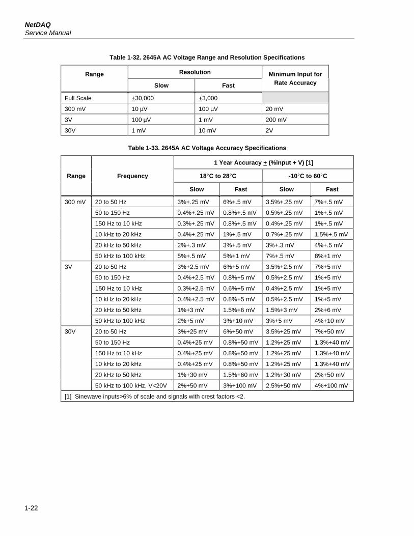
NetDAQService Manual
1-22
Table 1-32. 2645A AC Voltage Range and Resolution Specifications
Range Resolution Minimum Input for
Slow Fast Rate Accuracy
Full Scale +30,000 +3,000
300 mV 10 µV 100 µV 20 mV
3V 100 µV 1 mV 200 mV
30V 1 mV 10 mV 2V
Table 1-33. 2645A AC Voltage Accuracy Specifications
1 Year Accuracy + (%input + V) [1]
Range Frequency 18°C to 28°C -10°C to 60°C
Slow Fast Slow Fast
300 mV 20 to 50 Hz 3%+.25 mV 6%+.5 mV 3.5%+.25 mV 7%+.5 mV
50 to 150 Hz 0.4%+.25 mV 0.8%+.5 mV 0.5%+.25 mV 1%+.5 mV
150 Hz to 10 kHz 0.3%+.25 mV 0.8%+.5 mV 0.4%+.25 mV 1%+.5 mV
10 kHz to 20 kHz 0.4%+.25 mV 1%+.5 mV 0.7%+.25 mV 1.5%+.5 mV
20 kHz to 50 kHz 2%+.3 mV 3%+.5 mV 3%+.3 mV 4%+.5 mV
50 kHz to 100 kHz 5%+.5 mV 5%+1 mV 7%+.5 mV 8%+1 mV
3V 20 to 50 Hz 3%+2.5 mV 6%+5 mV 3.5%+2.5 mV 7%+5 mV
50 to 150 Hz 0.4%+2.5 mV 0.8%+5 mV 0.5%+2.5 mV 1%+5 mV
150 Hz to 10 kHz 0.3%+2.5 mV 0.6%+5 mV 0.4%+2.5 mV 1%+5 mV
10 kHz to 20 kHz 0.4%+2.5 mV 0.8%+5 mV 0.5%+2.5 mV 1%+5 mV
20 kHz to 50 kHz 1%+3 mV 1.5%+6 mV 1.5%+3 mV 2%+6 mV
50 kHz to 100 kHz 2%+5 mV 3%+10 mV 3%+5 mV 4%+10 mV
30V 20 to 50 Hz 3%+25 mV 6%+50 mV 3.5%+25 mV 7%+50 mV
50 to 150 Hz 0.4%+25 mV 0.8%+50 mV 1.2%+25 mV 1.3%+40 mV
150 Hz to 10 kHz 0.4%+25 mV 0.8%+50 mV 1.2%+25 mV 1.3%+40 mV
10 kHz to 20 kHz 0.4%+25 mV 0.8%+50 mV 1.2%+25 mV 1.3%+40 mV
20 kHz to 50 kHz 1%+30 mV 1.5%+60 mV 1.2%+30 mV 2%+50 mV
50 kHz to 100 kHz, V<20V 2%+50 mV 3%+100 mV 2.5%+50 mV 4%+100 mV
[1] Sinewave inputs>6% of scale and signals with crest factors <2.
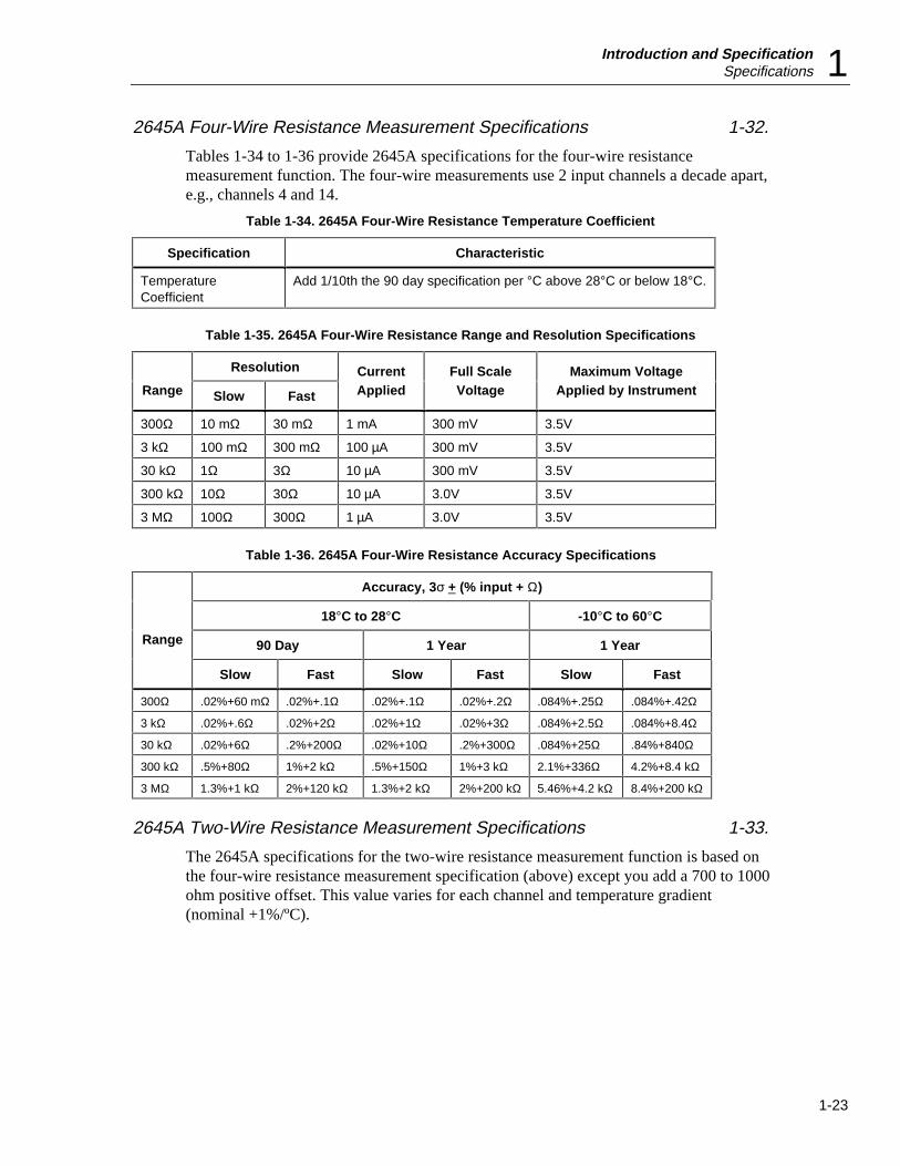
Introduction and SpecificationSpecifications 1
1-23
2645A Four-Wire Resistance Measurement Specifications 1-32.
Tables 1-34 to 1-36 provide 2645A specifications for the four-wire resistancemeasurement function. The four-wire measurements use 2 input channels a decade apart,e.g., channels 4 and 14.
Table 1-34. 2645A Four-Wire Resistance Temperature Coefficient
Specification Characteristic
TemperatureCoefficient
Add 1/10th the 90 day specification per °C above 28°C or below 18°C.
Table 1-35. 2645A Four-Wire Resistance Range and Resolution Specifications
Resolution Current Full Scale Maximum VoltageRange Slow Fast Applied Voltage Applied by Instrument
300Ω 10 mΩ 30 mΩ 1 mA 300 mV 3.5V
3 kΩ 100 mΩ 300 mΩ 100 µA 300 mV 3.5V
30 kΩ 1Ω 3Ω 10 µA 300 mV 3.5V
300 kΩ 10Ω 30Ω 10 µA 3.0V 3.5V
3 MΩ 100Ω 300Ω 1 µA 3.0V 3.5V
Table 1-36. 2645A Four-Wire Resistance Accuracy Specifications
Accuracy, 3σ + (% input + Ω)
18°C to 28°C -10°C to 60°C
Range 90 Day 1 Year 1 Year
Slow Fast Slow Fast Slow Fast
300Ω .02%+60 mΩ .02%+.1Ω .02%+.1Ω .02%+.2Ω .084%+.25Ω .084%+.42Ω
3 kΩ .02%+.6Ω .02%+2Ω .02%+1Ω .02%+3Ω .084%+2.5Ω .084%+8.4Ω
30 kΩ .02%+6Ω .2%+200Ω .02%+10Ω .2%+300Ω .084%+25Ω .84%+840Ω
300 kΩ .5%+80Ω 1%+2 kΩ .5%+150Ω 1%+3 kΩ 2.1%+336Ω 4.2%+8.4 kΩ
3 MΩ 1.3%+1 kΩ 2%+120 kΩ 1.3%+2 kΩ 2%+200 kΩ 5.46%+4.2 kΩ 8.4%+200 kΩ
2645A Two-Wire Resistance Measurement Specifications 1-33.
The 2645A specifications for the two-wire resistance measurement function is based onthe four-wire resistance measurement specification (above) except you add a 700 to 1000ohm positive offset. This value varies for each channel and temperature gradient(nominal +1%/ºC).
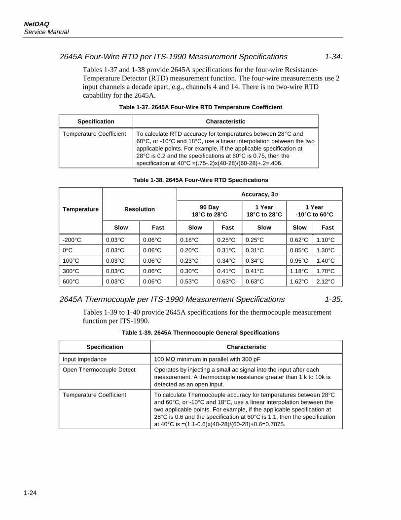
NetDAQService Manual
1-24
2645A Four-Wire RTD per ITS-1990 Measurement Specifications 1-34.
Tables 1-37 and 1-38 provide 2645A specifications for the four-wire Resistance-Temperature Detector (RTD) measurement function. The four-wire measurements use 2input channels a decade apart, e.g., channels 4 and 14. There is no two-wire RTDcapability for the 2645A.
Table 1-37. 2645A Four-Wire RTD Temperature Coefficient
Specification Characteristic
Temperature Coefficient To calculate RTD accuracy for temperatures between 28°C and60°C, or -10°C and 18°C, use a linear interpolation between the twoapplicable points. For example, if the applicable specification at28°C is 0.2 and the specifications at 60°C is 0.75, then thespecification at 40°C =(.75-.2)x(40-28)/(60-28)+.2=.406.
Table 1-38. 2645A Four-Wire RTD Specifications
Accuracy, 3σ
Temperature Resolution 90 Day18°C to 28°C
1 Year18°C to 28°C
1 Year-10°C to 60°C
Slow Fast Slow Fast Slow Slow Fast
-200°C 0.03°C 0.06°C 0.16°C 0.25°C 0.25°C 0.62°C 1.10°C
0°C 0.03°C 0.06°C 0.20°C 0.31°C 0.31°C 0.85°C 1.30°C
100°C 0.03°C 0.06°C 0.23°C 0.34°C 0.34°C 0.95°C 1.40°C
300°C 0.03°C 0.06°C 0.30°C 0.41°C 0.41°C 1.18°C 1.70°C
600°C 0.03°C 0.06°C 0.53°C 0.63°C 0.63°C 1.62°C 2.12°C
2645A Thermocouple per ITS-1990 Measurement Specifications 1-35.
Tables 1-39 to 1-40 provide 2645A specifications for the thermocouple measurementfunction per ITS-1990.
Table 1-39. 2645A Thermocouple General Specifications
Specification Characteristic
Input Impedance 100 MΩ minimum in parallel with 300 pF
Open Thermocouple Detect Operates by injecting a small ac signal into the input after eachmeasurement. A thermocouple resistance greater than 1 k to 10k isdetected as an open input.
Temperature Coefficient To calculate Thermocouple accuracy for temperatures between 28°Cand 60°C, or -10°C and 18°C, use a linear interpolation between thetwo applicable points. For example, if the applicable specification at28°C is 0.6 and the specification at 60°C is 1.1, then the specificationat 40°C is =(1.1-0.6)x(40-28)/(60-28)+0.6=0.7875.
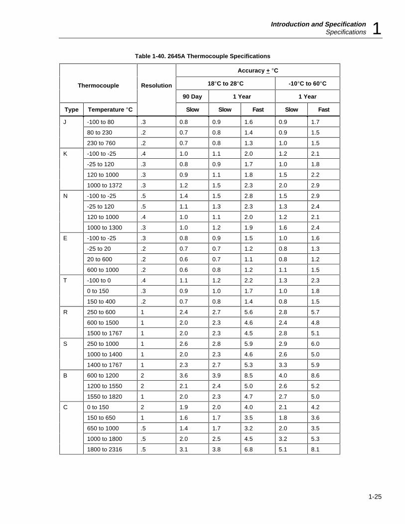
Introduction and SpecificationSpecifications 1
1-25
Table 1-40. 2645A Thermocouple Specifications
Accuracy + °C
Thermocouple Resolution 18°C to 28°C -10°C to 60°C
90 Day 1 Year 1 Year
Type Temperature °C Slow Slow Fast Slow Fast
J -100 to 80 .3 0.8 0.9 1.6 0.9 1.7
80 to 230 .2 0.7 0.8 1.4 0.9 1.5
230 to 760 .2 0.7 0.8 1.3 1.0 1.5
K -100 to -25 .4 1.0 1.1 2.0 1.2 2.1
-25 to 120 .3 0.8 0.9 1.7 1.0 1.8
120 to 1000 .3 0.9 1.1 1.8 1.5 2.2
1000 to 1372 .3 1.2 1.5 2.3 2.0 2.9
N -100 to -25 .5 1.4 1.5 2.8 1.5 2.9
-25 to 120 .5 1.1 1.3 2.3 1.3 2.4
120 to 1000 .4 1.0 1.1 2.0 1.2 2.1
1000 to 1300 .3 1.0 1.2 1.9 1.6 2.4
E -100 to -25 .3 0.8 0.9 1.5 1.0 1.6
-25 to 20 .2 0.7 0.7 1.2 0.8 1.3
20 to 600 .2 0.6 0.7 1.1 0.8 1.2
600 to 1000 .2 0.6 0.8 1.2 1.1 1.5
T -100 to 0 .4 1.1 1.2 2.2 1.3 2.3
0 to 150 .3 0.9 1.0 1.7 1.0 1.8
150 to 400 .2 0.7 0.8 1.4 0.8 1.5
R 250 to 600 1 2.4 2.7 5.6 2.8 5.7
600 to 1500 1 2.0 2.3 4.6 2.4 4.8
1500 to 1767 1 2.0 2.3 4.5 2.8 5.1
S 250 to 1000 1 2.6 2.8 5.9 2.9 6.0
1000 to 1400 1 2.0 2.3 4.6 2.6 5.0
1400 to 1767 1 2.3 2.7 5.3 3.3 5.9
B 600 to 1200 2 3.6 3.9 8.5 4.0 8.6
1200 to 1550 2 2.1 2.4 5.0 2.6 5.2
1550 to 1820 1 2.0 2.3 4.7 2.7 5.0
C 0 to 150 2 1.9 2.0 4.0 2.1 4.2
150 to 650 1 1.6 1.7 3.5 1.8 3.6
650 to 1000 .5 1.4 1.7 3.2 2.0 3.5
1000 to 1800 .5 2.0 2.5 4.5 3.2 5.3
1800 to 2316 .5 3.1 3.8 6.8 5.1 8.1
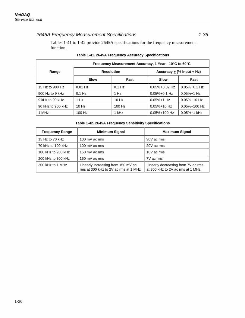
NetDAQService Manual
1-26
2645A Frequency Measurement Specifications 1-36.
Tables 1-41 to 1-42 provide 2645A specifications for the frequency measurementfunction.
Table 1-41. 2645A Frequency Accuracy Specifications
Frequency Measurement Accuracy, 1 Year, -10°C to 60°C
Range Resolution Accuracy + (% input + Hz)
Slow Fast Slow Fast
15 Hz to 900 Hz 0.01 Hz 0.1 Hz 0.05%+0.02 Hz 0.05%+0.2 Hz
900 Hz to 9 kHz 0.1 Hz 1 Hz 0.05%+0.1 Hz 0.05%+1 Hz
9 kHz to 90 kHz 1 Hz 10 Hz 0.05%+1 Hz 0.05%+10 Hz
90 kHz to 900 kHz 10 Hz 100 Hz 0.05%+10 Hz 0.05%+100 Hz
1 MHz 100 Hz 1 kHz 0.05%+100 Hz 0.05%+1 kHz
Table 1-42. 2645A Frequency Sensitivity Specifications
Frequency Range Minimum Signal Maximum Signal
15 Hz to 70 kHz 100 mV ac rms 30V ac rms
70 kHz to 100 kHz 100 mV ac rms 20V ac rms
100 kHz to 200 kHz 150 mV ac rms 10V ac rms
200 kHz to 300 kHz 150 mV ac rms 7V ac rms
300 kHz to 1 MHz Linearly increasing from 150 mV acrms at 300 kHz to 2V ac rms at 1 MHz
Linearly decreasing from 7V ac rmsat 300 kHz to 2V ac rms at 1 MHz
2-1
Chapter 2Theory of Operation
Title Page
2-1. Introduction ............................................................................................ 2-52-2. Functional Block Description................................................................. 2-52-3. A1 Main PCA Block Description ...................................................... 2-72-4. Power Supply................................................................................ 2-72-5. Digital Kernel ............................................................................... 2-72-6. Serial Communication (Guard Crossing) ..................................... 2-82-7. Digital Inputs and Outputs............................................................ 2-82-8. Ethernet Interface ......................................................................... 2-82-9. A2 Display PCA Block Description .................................................. 2-82-10. A3 A/D Converter PCA Block Description....................................... 2-82-11. Analog Measurement Processor ................................................... 2-92-12. Input Protection ............................................................................ 2-92-13. Input Signal Conditioning ............................................................ 2-92-14. Analog-to-Digital (a/d) Converter................................................ 2-92-15. Inguard Microcontroller ............................................................... 2-92-16. Channel Selection......................................................................... 2-92-17. Open Thermocouple Check.......................................................... 2-102-18. A4 Analog Input PCA Block Description ......................................... 2-102-19. 20-Channel Terminals .................................................................. 2-102-20. Reference Junction Temperature.................................................. 2-102-21. Detailed Circuit Description .................................................................. 2-102-22. A1 Main PCA Circuit Description..................................................... 2-102-23. Power Supply Circuit Description................................................ 2-102-24. Raw DC Supply ........................................................................ 2-112-25. Auxiliary 6V Supply................................................................. 2-112-26. 5V Switcher .............................................................................. 2-112-27. Inverter...................................................................................... 2-122-28. Inverter Outguard Supply ......................................................... 2-122-29. Inverter Inguard Supply............................................................ 2-132-30. Power Fail Detection ................................................................ 2-13
NetDAQService Manual
2-2
2-31. Digital Kernel ............................................................................... 2-132-32. Reset Circuits............................................................................ 2-142-33. Microprocessor ......................................................................... 2-142-34. Address Decoding..................................................................... 2-162-35. Flash Memory........................................................................... 2-182-36. Static RAM ............................................................................... 2-182-37. Real-Time Clock....................................................................... 2-192-38. FPGA (Field Programmable Gate Array)................................. 2-192-39. Serial Communication (Guard Crossing) ................................. 2-212-40. RS-232 Interface....................................................................... 2-212-41. Ethernet Interface ..................................................................... 2-222-42. Digital Inputs and Outputs............................................................ 2-242-43. Digital Input Threshold ............................................................ 2-242-44. Digital Input Buffers................................................................. 2-242-45. Digital and Alarm Output Drivers ............................................ 2-252-46. Totalizer Input .......................................................................... 2-252-47. External Trigger Circuits .......................................................... 2-252-48. A2 Display PCA Circuit Description................................................. 2-262-49. Main PCA Connector ................................................................... 2-262-50. Front Panel Switches .................................................................... 2-272-51. Display.......................................................................................... 2-282-52. Beeper Drive Circuit..................................................................... 2-282-53. Watchdog Timer and Reset Circuit .............................................. 2-292-54. Display Controller ........................................................................ 2-292-55. A3 A/D Converter PCA Circuit Description ..................................... 2-312-56. Stallion Chip................................................................................. 2-332-57. Input Protection ............................................................................ 2-332-58. Input Signal Conditioning ............................................................ 2-332-59. Function Relays ............................................................................ 2-332-60. Channel Selection Circuitry ......................................................... 2-342-61. DC Volts and Thermocouples Measurement Circuitry................ 2-342-62. Ohms and RTD Measurement Circuitry....................................... 2-362-63. AC Volts Measurement Circuitry................................................. 2-372-64. Frequency Measurements............................................................. 2-372-65. Active Filter (ACV Filter) ............................................................ 2-372-66. Voltage Reference Circuit ............................................................ 2-382-67. Analog/Digital Converter Circuit ................................................. 2-392-68. Autozero ................................................................................... 2-392-69. Integrate .................................................................................... 2-402-70. Deintegrate1.............................................................................. 2-422-71. Deintegrate2.............................................................................. 2-422-72. Overhead................................................................................... 2-422-73. Inguard Digital Kernel Circuitry .................................................. 2-422-74. Open Thermocouple Detect Circuitry............................................ 2-432-75. A4 Analog Input PCA Circuit Description........................................ 2-432-76. A1 Main to A3 A/D Converter Communications .................................. 2-442-77. Special Codes..................................................................................... 2-442-78. Resets ................................................................................................. 2-44
Theory of OperationIntroduction 2
2-3
2-79. Commands ......................................................................................... 2-452-80. Perform Scan ................................................................................ 2-452-81. Perform Self-Test ......................................................................... 2-462-82. Return Main Firmware Version.................................................... 2-462-83. Return Boot Firmware Version .................................................... 2-472-84. Set Global Configuration.............................................................. 2-472-85. Set Channel Configuration ........................................................... 2-472-86. Do Housekeeping ......................................................................... 2-482-87. Checksums ......................................................................................... 2-482-88. Errors.................................................................................................. 2-482-89. Power-Up Protocol............................................................................. 2-492-90. Inguard Unresponsive ........................................................................ 2-492-91. Inguard Software Description ................................................................ 2-492-92. Hardware Elements ............................................................................ 2-492-93. Channel MUX............................................................................... 2-492-94. Function Relays ............................................................................ 2-512-95. Stallion Chip and Signal Conditioning......................................... 2-512-96. A/D ............................................................................................... 2-532-97. Timing ...................................................................................... 2-542-98. Control Signals ......................................................................... 2-542-99. Counters.................................................................................... 2-562-100. Converting Counts to Volts ...................................................... 2-562-101. DISCHARGE Signal .................................................................... 2-572-102. Open-Thermocouple Detector ...................................................... 2-572-103. Channel Measurements...................................................................... 2-572-104. Reading Rates ............................................................................... 2-572-105. Measurement Types...................................................................... 2-582-106. VDC, VAC, Ohms.................................................................... 2-582-107. VDC Fast Rate, 2645A............................................................. 2-582-108. Thermocouples ......................................................................... 2-592-109. Reference Junction ................................................................... 2-592-110. Frequency ................................................................................. 2-592-111. VAC Discharge Mode .............................................................. 2-602-112. Autoranging .................................................................................. 2-602-113. Overload ....................................................................................... 2-612-114. Housekeeping Readings..................................................................... 2-612-115. Reading Types .............................................................................. 2-612-116. Reference Balance Readings .................................................... 2-612-117. Zero Offset Readings................................................................ 2-622-118. Housekeeping Schedule................................................................ 2-622-119. Self-Tests ........................................................................................... 2-622-120. Power-Up Self-Tests .................................................................... 2-622-121. Self-Test Command...................................................................... 2-632-122. A/D Test.................................................................................... 2-632-123. Zero Offset Test........................................................................ 2-632-124. Reference Balance Test ............................................................ 2-632-125. Ohms Overload Test ................................................................. 2-632-126. OTC Test .................................................................................. 2-63

NetDAQService Manual
2-4
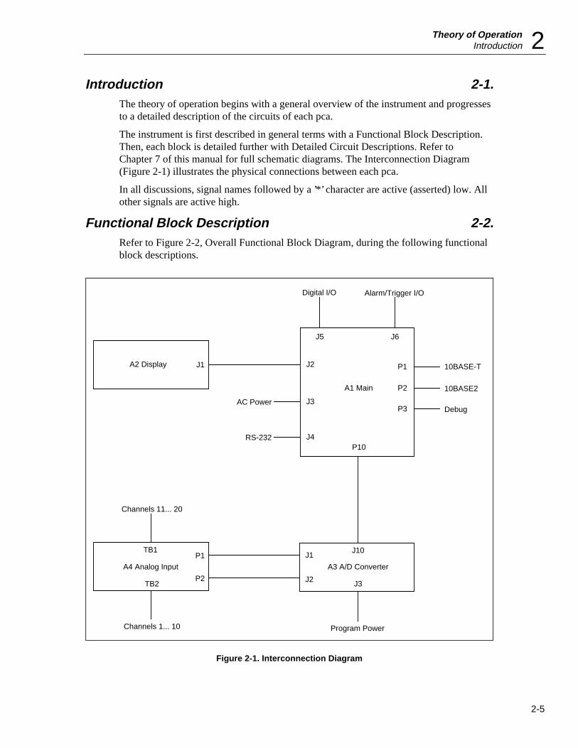
Theory of OperationIntroduction 2
2-5
Introduction 2-1.The theory of operation begins with a general overview of the instrument and progressesto a detailed description of the circuits of each pca.
The instrument is first described in general terms with a Functional Block Description.Then, each block is detailed further with Detailed Circuit Descriptions. Refer toChapter 7 of this manual for full schematic diagrams. The Interconnection Diagram(Figure 2-1) illustrates the physical connections between each pca.
In all discussions, signal names followed by a ’*’ character are active (asserted) low. Allother signals are active high.
Functional Block Description 2-2.Refer to Figure 2-2, Overall Functional Block Diagram, during the following functionalblock descriptions.
J4
J2
J6J5
J3
P10
P1
P2
P3
A1 Main
A2 Display J1
RS-232
Alarm/Trigger I/ODigital I/O
AC Power
10BASE2
10BASE-T
Debug
Program Power
J1
J2 J3
A3 A/D Converter
J10P1
P2
A4 Analog Input
TB1
TB2
Channels 11... 20
Channels 1... 10
Figure 2-1. Interconnection Diagram
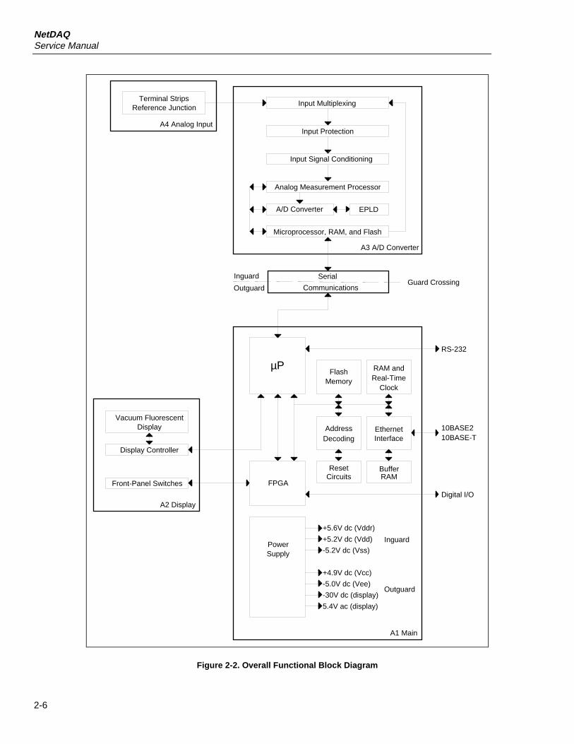
NetDAQService Manual
2-6
A4 Analog InputInput Protection
A/D Converter
Microprocessor, RAM, and Flash
EPLD
Analog Measurement Processor
Terminal StripsReference Junction
A3 A/D Converter
Input Signal Conditioning
SerialInguard
OutguardGuard Crossing
FlashMemory
RAM andReal-Time
Clock
RS-232
10BASE210BASE-T
ResetCircuits
AddressDecoding
EthernetInterface
BufferRAM
Digital I/OA2 Display
Front-Panel Switches
Display Controller
Vacuum FluorescentDisplay
PowerSupply
Inguard
Outguard
+5.6V dc (Vddr)
+5.2V dc (Vdd)
-5.2V dc (Vss)
+4.9V dc (Vcc)
-30V dc (display)
5.4V ac (display)
-5.0V dc (Vee)
A1 Main
Input Multiplexing
FPGA
Communications
µP
Figure 2-2. Overall Functional Block Diagram
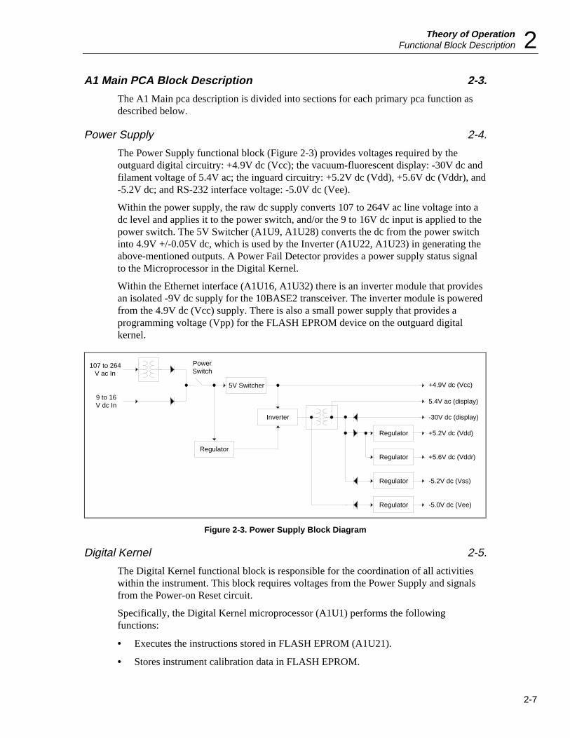
Theory of OperationFunctional Block Description 2
2-7
A1 Main PCA Block Description 2-3.
The A1 Main pca description is divided into sections for each primary pca function asdescribed below.
Power Supply 2-4.
The Power Supply functional block (Figure 2-3) provides voltages required by theoutguard digital circuitry: +4.9V dc (Vcc); the vacuum-fluorescent display: -30V dc andfilament voltage of 5.4V ac; the inguard circuitry: +5.2V dc (Vdd), +5.6V dc (Vddr), and-5.2V dc; and RS-232 interface voltage: -5.0V dc (Vee).
Within the power supply, the raw dc supply converts 107 to 264V ac line voltage into adc level and applies it to the power switch, and/or the 9 to 16V dc input is applied to thepower switch. The 5V Switcher (A1U9, A1U28) converts the dc from the power switchinto 4.9V +/-0.05V dc, which is used by the Inverter (A1U22, A1U23) in generating theabove-mentioned outputs. A Power Fail Detector provides a power supply status signalto the Microprocessor in the Digital Kernel.
Within the Ethernet interface (A1U16, A1U32) there is an inverter module that providesan isolated -9V dc supply for the 10BASE2 transceiver. The inverter module is poweredfrom the 4.9V dc (Vcc) supply. There is also a small power supply that provides aprogramming voltage (Vpp) for the FLASH EPROM device on the outguard digitalkernel.
5V Switcher
Inverter
Regulator
Regulator
Regulator
Regulator
Regulator
PowerSwitch
107 to 264V ac In
9 to 16V dc In
+4.9V dc (Vcc)
5.4V ac (display)
-30V dc (display)
+5.2V dc (Vdd)
+5.6V dc (Vddr)
-5.2V dc (Vss)
-5.0V dc (Vee)
Figure 2-3. Power Supply Block Diagram
Digital Kernel 2-5.
The Digital Kernel functional block is responsible for the coordination of all activitieswithin the instrument. This block requires voltages from the Power Supply and signalsfrom the Power-on Reset circuit.
Specifically, the Digital Kernel microprocessor (A1U1) performs the followingfunctions:
• Executes the instructions stored in FLASH EPROM (A1U21).
• Stores instrument calibration data in FLASH EPROM.
NetDAQService Manual
2-8
• Communicates with the microprocessor on the A/D Converter PCA via the SerialCommunication (Guard Crossing) block (A1U5, A1U7).
• Communicates with the Display Controller to display readings and user interfaceinformation (A1U1, A1U31).
• Communicates with the Field Programmable Gate Array (A1U31), which scans theuser interface keyboard found on the Display Assembly and interfaces with theDigital I/O hardware.
• Communicates with a host computer via the Ethernet interface (A1U32).
• Communicates with a host computer via the RS-232 interface (A1U1, A1U13).
• Reads the digital inputs and changes digital, alarm, and trigger outputs.
Serial Communication (Guard Crossing) 2-6.
This functional block provides a high isolation voltage communication path between theDigital Kernel of the Main PCA and the microprocessor on the A/D Converter PCA.This bidirectional communication circuit (A1U5, A1U7) requires power supply voltagesfrom the Power Supply block.
Digital Inputs and Outputs 2-7.
This functional block contains the Totalizer and Trigger Input buffers, eight bidirectionalDigital I/O channels (A1U3, A1U4, A1U17, A1U27), Master Alarm output, and aTrigger Output (A1U17). These circuits require power supply voltages from the PowerSupply and signals from the Digital Kernel.
Ethernet Interface 2-8.
This functional block contains the Ethernet Controller (A1U32), used for both 10BASE2and 10BASE-T. When 10BASE2 is selected by the Ethernet interface, an additionalEthernet Transceiver device (A1U32) is used. These circuits require power supplyvoltages from the Power Supply and signals from the Digital Kernel.
A2 Display PCA Block Description 2-9.
The Display Assembly controller communicates with the A1 Main PCA microprocessor(A1U1) over a three-wire communication channel. Commands from the microprocessorinform the Display Controller how to modify its internal display memory. The DisplayController (A2U1) then drives the grid and anode signals to illuminate the requiredsegments on the Display. The A2 Display PCA requires power supply voltages from theA1 Main PCA power supply voltages and a clock signal from the A1U4 microprocessor.
A3 A/D Converter PCA Block Description 2-10.
The following paragraphs describe the major blocks of circuitry on the A/D ConverterPCA.
Theory of OperationFunctional Block Description 2
2-9
Analog Measurement Processor 2-11.
The Analog Measurement Processor (A3U30) provides input signal conditioning,ranging, and frequency measurement. This custom chip is controlled by the A/DMicroprocessor (A3U5). The A/D Microprocessor communicates with the Main PCAMicroprocessor (A1U1) over a serial interface.
Input Protection 2-12.
This circuitry protects the instrument measurement circuits during overvoltageconditions.
Input Signal Conditioning 2-13.
Here, each input is conditioned and/or scaled to a dc voltage for measurement by the a/dconverter. DC voltage levels greater than 3V are attenuated. To measure resistance, a dccurrent is applied across a series connection of the input resistance and a referenceresistance to develop dc voltages that can be ratioed. DC volts and ohms measurementsare filtered by a passive filter. AC voltages are first scaled by an ac buffer, converted to arepresentative dc voltage by an rms converter, and then filtered by an active filter.
Analog-to-Digital (a/d) Converter 2-14.
The dc voltage output from the signal conditioning circuits is applied to a multi-slopeA/D converter.
The input voltage is applied to a buffer/integrator that charges a capacitor for an exactamount of time. During this time, positive and negative reference voltages are alternatelyapplied to the integrator. The references are switched in a sequence controlled by theA/D Electrically Programmed Logic Device (EPLD) (A3U18), which prevents theintegrator from saturating.
The amount of time that each reference is applied to the integrator, and the amount oftime required to discharge the capacitor, are measured by digital counter circuits in theA/D EPLD (A3U18). These times are used by the inguard microprocessor (A3U5) tocalculate the level of the unknown input signal.
Inguard Microcontroller 2-15.
This microprocessor (A3U5) and associated circuitry controls all functions on the A/DConverter PCA and communicates with the digital kernel on the Main PCA. Uponrequest by the Main PCA, the inguard microprocessor selects the input channel to bemeasured through the channel selection circuitry, sets up the input signal conditioning,commands the A/D EPLD (A3U18) to begin a conversion, stops the measurement, andthen fetches the measurement result. The inguard microprocessor manipulates the resultmathematically and transmits the reading to the digital kernel.
Channel Selection 2-16.
This circuitry consists of a set of relays and relay-control drivers. The relays form a treethat routes the input channels to the measurement circuitry. Two of the relays are alsoused to switch between two-wire and four-wire operation. For signal switching andselection, the 2640A uses reed relays, while the 2645A uses solid-state relays.
NetDAQService Manual
2-10
Open Thermocouple Check 2-17.
Under control of the Inguard Microprocessor, the open thermocouple check circuitapplies a small ac signal to a thermocouple input before each measurement. If anexcessive resistance is encountered, an open thermocouple input condition is reported.
A4 Analog Input PCA Block Description 2-18.
The following paragraphs briefly describe the major sections of the Input ConnectorPCA, which is the “Universal Input Module” used for connecting the analog inputs to theinstrument.
20-Channel Terminals 2-19.
Twenty HI and LO terminal blocks are provided in two rows, one for channels 1 through10 and one for channels 11 through 20. The terminals can accommodate a wide range ofwire sizes, starting with 12 gauge as the largest size. The two rows of terminal blocks aremaintained very close to the same temperature for accurate thermocouple measurements.
Reference Junction Temperature 2-20.
A semiconductor junction is used to sense the temperature of the thermocouple inputterminals. The resulting dc output voltage is proportional to the block temperature and issent to the A/D Converter PCA for measurement.
Detailed Circuit Description 2-21.The following circuit descriptions describe the theory of operation for each Instrumentpca. For these descriptions, refer to the associated schematic diagram in Chapter 7.
A1 Main PCA Circuit Description 2-22.
The following paragraphs describe the operation of the circuits on the A1 Main PCA.The schematic for this pca is located in Chapter 7.
Power Supply Circuit Description 2-23.
The power supply portion of the A1 Main pca consists of three major sections:
• Raw DC Supply The raw dc supply converts line voltage (107V to 264V ac) into adc output of 8V to 35V.
• 5V Switcher Supply The 5V switcher supply regulates the 8V to 35V dc input intothe 4.9V +/-0.05V dc (Vcc) source.
• Inverter Using the 5V switching supply output, the inverter generates the -30V dcand 5.4V ac supply levels needed for the vacuum-fluorescent display and the -5V dcsupply for the RS-232 Interface. The inverter also provides isolated +5.6V (Vddr),+5.2V (Vdd), and -5.2V (Vss) outputs for the inguard circuitry.
Theory of OperationDetailed Circuit Description 2
2-11
Raw DC Supply 2-24.
The raw dc supply circuitry receives input from power transformer T401, which operatesfrom an ac source of 107V to 264V ac. The power transformer is energized whenever thepower cord is plugged into the ac line; there is no on/off switch on the primary side ofthe transformer. The transformer has an internal 275V ac metal-oxide varistor (MOV) toclamp line transients. The MOV normally acts as an open circuit. When the peak voltageexceeds approximately 400V, the line impedance in series with the line fuse limitstransients to approximately 450V. All line voltages use a time-delay 0.15 A, 250V fuse.
On the secondary side of the transformer, rectifiers A1CR2, A1CR3, and capacitor A1C7rectify and filter the output. When ON, switch A1S1 (the rear panel POWER switch)connects the output of the rectifiers to the filter capacitor and the rest of the instrument.Depending on line voltage, the output of the rectifiers is between 8.0 and 35V dc.Capacitor A1C2 is used for electromagnetic interference (EMI) and electromagneticcompatibility (EMC) requirements. Capacitor A1C1 helps supply the high frequencyripple current drawn by the switching regulator (described below).
When external dc power is used, the power switch connects the external dc source topower the instrument. The external dc input uses thermistor A1RT1 for overcurrentprotection and diode A1CR1 for reverse input voltage protection. Capacitor A1C59 isused for EMI/EMC requirements. Resistor A1R48, and capacitors A1C102 and A1C39are also used for EMI/EMC performance requirements. If both ac power and dc powerare connected to the instrument, the instrument uses ac power when it exceedsapproximately eight times the value of the dc voltage. Automatic switchover occursbetween ac and dc power without interrupting instrument operation.
Auxiliary 6V Supply 2-25.
Three-terminal regulator A1U19, voltage-setting resistors A1R44 and A1R46, andcapacitor A1C34, make up the auxiliary 6-volt supply. This supply is used to power theinverter oscillator and inverter driver.
5V Switcher 2-26.
The 5V switcher supply uses a controller/switch device A1U9 and related circuitry toproduce the 4.9V dc (Vcc) output.
4.9V dc (Vcc) The 8V to 35V dc input is regulated to 4.9V dc (Vcc) throughpulse-width modulation at a nominal switching frequency of 100 kHz. The outputvoltage of the switcher supply is controlled by varying the duty cycle (ON time) of theswitching transistor in the controller/switch device A1U9. A1U9 contains the supplyreference, oscillator, switch transistor, pulse-width modulator comparator, switch drivecircuit, current-limit comparator, current-limit reference, and thermal limit. Dualinductor A1T2 regulates the current that flows from the raw supply to the load as theswitching transistor in A1U9 is turned on and off. Complementary switch A1CR10conducts when switching is turned off.
NetDAQService Manual
2-12
The pulse-width modulator comparator in A1U9 compares the output to an internalreference and sets the ON-time/OFF-time ratio to regulate the output to 4.9V dc. A1C1is the input filter capacitor, and A1C14 and A1C18 are the output filter capacitors.Proper inductor and capacitor values set the filter frequency response to ensure bestoverall system stability. A1R26 and A1C21 ensure that the switcher supply remainsstable and operating in the continuous mode. The power supply current is internallylimited by A1U9 to 5 amps.
Resistors A1R5, A1R6, A1R27, A1R29, A1R30 and A1R31 form a voltage divider thatoperates in conjunction with amplifier A1U28, which is configured as a voltagefollower. A1U28-3 samples the 4.9V dc output, while A1U28-2 is the voltage dividerinput. The effect is to maintain the junction of R30 and R31 at 4.9V dc, resulting in anA1U28-1 output level of 6.14V dc, or 1.24V dc above the output This feedback voltageis applied to A1U9-2, which A1U9 interprets as 1.24V dc because A1U9-3 (ground) isconnected to the 4.9V dc output. A1U9 maintains the feedback and reference voltages at1.24V dc and thus regulates the 4.9V dc source.
Inverter 2-27.
The inverter supply uses a two transistor-driven push-pull configuration. The center tapof transformer A1T1 primary is connected to the 4.9V dc Vcc supply, and each side isalternately connected to common through transistors A1Q7 and A1Q8. A1R38 may beremoved to disable the inverter supply for troubleshooting purposes. A1Q7 and A1Q8are driven by the outputs of D flip-flop A1U22. Resistors A1R34 and A1R28, and diodesA1CR11 and A1CR12 shape the input drive signals to properly drive the gate of thetransistors. D flip-flop A1U22 is wired as a divide-by-two counter driven by a 110-kHzsquare wave. The 110-kHz square wave is generated by hex inverter A1U23, which isconnected as an oscillator with a frequency determined by the values of resistors A1R40and A1R47, and capacitor A1C35. The resulting ac voltage produced across thesecondary of A1T1 is rectified to provide the input to the inverter inguard and outguardsupplies.
Inverter Outguard Supply 2-28.
The inverter outguard supply provides three outputs: -30V dc and 5.4V ac for thedisplay, and -5.0V dc (Vee) for the RS-232 drivers and receiver.
-30V dc Dual diodes A1CR8 and A1CR9 provide full-wave rectification of A1T1outputs (pins 4, 5, and 8), creating the -30V dc supply. Output filtering for the -30V dcsupply is provided by capacitor A1C17.
5.4V ac The 5.4V ac supply is sourced from a secondary winding on transformer T1(pins 6 and 7), and is biased at -24V dc with zener diode A1VR3 and resistor A1R22.
-5.0V dc (Vee) Dual-diode A1CR13 rectifies an input from the inverter circuit, with thediode and capacitors A1C30 and A1C31 configured as a voltage doubler, generating-12V dc. This voltage is applied to the three-terminal regulator A1U18, which regulatesthe output for the -5.0V dc (Vee) source. Capacitor A1C32 is used for transient responseperformance of the three-terminal regulator.
Theory of OperationDetailed Circuit Description 2
2-13
Inverter Inguard Supply 2-29.
The inverter inguard supply provides three outputs: +5.2V dc (Vdd) and -5.2V dc (Vss)for the inguard analog and digital circuitry, and +5.6V dc (Vddr) for the relays. DiodesA1CR5 and A1CR6, and capacitor A1C12 create a +6.8V dc source, while diodesA1CR7 and capacitor A1C13 create a -9.5V dc source.
+5.2V dc (Vdd) The +5.2V dc (Vdd) source is regulated from a +6.8V dc input toA1U24 with resistors A1R9 and A1R10 setting the output voltage, and A1C4 handlingtransient loads. Resistors A1R4, A1R130, A1R128 and A1R13, along with transistorA1Q1, comprise a current-limiting circuit, which prevents A1U24 from supplying morethan 60 mA of load current.
-5.2V dc (Vss) The -5.2V dc (Vss) source is regulated from a -9.5V dc input to A1U25with resistors A1R11 and A1R12 setting the output voltage, and A1C5 handling transientloads. Resistors A1R14, A1R15, A1R129, A1R122, along with transistors A1Q5 andA1Q6, comprise a current-limiting circuit, which prevents A1U25 from supplying morethan 40 mA of load current. Capacitor A1C9 enables the regulator to start up.
+5.6V dc (Vddr) The +5.6V dc (Vddr) source is regulated from a +6.8V dc input toA1U6 with resistors A1R131 and A1R132 setting the output voltage, and A1C6 handlingtransient loads.
Power Fail Detection 2-30.
The power fail detection circuit generates a signal to warn the Microprocessor that thepower supply is going down. Microprocessor supervisor A1U10 compares thedivided-down raw supply voltage, via voltage divider A1R19 and A1R20. When the rawsupply voltage falls below approximately 8V dc, A1U10-5 output is low. ResistorA1R99 is a pull up resistor for the A1U10-7 reset line, and A1C81 provides filtering ofhigh frequency noise. The reference voltage internal to the A1U10 is nominally 1.3V dc.
Digital Kernel 2-31.
The Digital Kernel is composed of the following 10 functional circuit blocks:
• Reset Circuits
• Microprocessor
• Address Decoding
• Flash Memory
• Static RAM
• Real-Time Clock
• FPGA (Field Programmable Gate Array)
• Serial Communication (Guard Crossing)
• RS-232 Interface
• Ethernet Interface
Each of the 10 topics is discussed below.
NetDAQService Manual
2-14
Reset Circuits 2-32.
The Power-On Reset signal (POR*, A1U10-7) is generated by the MicroprocessorSupervisor, which monitors the voltage of Vcc at A1U10-2. If Vcc is less than +4.65volts, then A1U10-7 is driven low. POR* drives the enable inputs of the four tri-statebuffers in A1U2, causing the HALT*, RESET*, and DRST* signals to be driven lowwhen POR* is low. When POR* goes high, the tri-state buffer outputs (A1U2) go totheir high-impedance state and the pull-up resistors pull the outputs to a high level.
When HALT* and RESET* are both driven low, the Microprocessor (A1U1) is reset andis in execution when they both go high. The Microprocessor may execute a "reset"instruction during normal operation to drive A1U1-92 low for approximately 10microseconds to reset all system hardware connected to the RESET* signal.
The Display Reset signal (DRST*) is driven low by A1U2-6 when POR* is low, or itmay be driven low by the Microprocessor (A1U1-56) if the instrument firmware needs toreset only the display hardware. For example, the firmware resets the display hardwareafter the FPGA is loaded at power-up and the Display Clock (DCLK) signal from theFPGA begins normal operation. This ensures that the Display Processor is properly resetwhile DCLK is active.
Microprocessor 2-33.
The Microprocessor uses a 16-bit data bus and a 20-bit address bus to access locations inthe Flash Memory (A1U21), the Static RAM (A1U20, A1U30, A1U34 and A1U35), theReal-Time Clock (A1U11), the FPGA (A1U31), and the Ethernet Interface (A1U32). Allof the data bus lines and the lowest 12 address lines have series termination resistorslocated near the Microprocessor (A1U1) to ensure that the instrument meets EMI/EMCperformance requirements. When a memory access is done to the upper half of the databus (D15 through D8), the upper data strobe (UDS*) goes low. When a memory accessis done to the lower half of the data bus (D7 through D0), the lower data strobe (LDS*)goes low. When a memory access is a read cycle, R/W* must be high. Conversely forany write cycle, R/W* must be low.
The Microprocessor is a variant of the popular Motorola 68000 processor and isenhanced by including hardware support for clock generation, address decoding, timers,parallel ports, synchronous and asynchronous serial communications, interruptcontroller, DMA (Direct Memory Access) controllers, and a watchdog timer.
The 15.36-MHz system clock signal (A1TP11) is generated by the oscillator circuitcomposed of A1U1, A1Y1, A1R2, A1C3, and A1C8. This clock goes through a seriestermination resistor (A1R17) to the FPGA (A1U31). This resistor is necessary to ensurethat the instrument meets EMI/EMC performance requirements.
The Microprocessor has four software programmed address decoders that include waitstate control logic. These four outputs are used to enable external memory and I/Ocomponents during read and write bus cycles. See "Address Decoding" for a completedescription.
Theory of OperationDetailed Circuit Description 2
2-15
One sixteen-bit timer in the Microprocessor is used to keep track of the time to thenearest millisecond. The timer counter runs off the 15.36 MHz clock at a rate of 1/64thmillisecond. The CINT* signal from the Real Time Clock chip (A1U11) causes the timercounter to be sampled every 1/64th of a second. The CINT* signal also interrupts theMicroprocessor to provide a timing reference for the software. The combination of thecounter and the interrupt are used by the software to keep track of the time to the nearestmillisecond, referenced to the Real Time Clock Chip.
A second sixteen-bit timer in the Microprocessor is used for an interval timer. It is alsoclocked at a rate of 1/64th millisecond. This timer interrupts the Microprocessor at a ratedetermined by the application.
The Microprocessor has two parallel ports. Many of the parallel port pins are either usedas software controlled signals or as inputs or outputs of timers and serial communicationchannels. Port A has 16 bits and Port B has 12 bits.
The Microprocessor communicates to the Display Controller using a synchronous,three-wire communication interface controlled by hardware in the Microprocessor.Information is communicated to the Display Controller to display user interface menusand measurement data. Details of this communication are described in the DisplayController Theory of Operation in this chapter.
The Microprocessor communicates to the A/D Microprocessor on the A/D ConverterPCA (via the Serial Communication circuit) using an asynchronous communicationchannel at 120,000 baud. Communication to the A/D Microprocessor (A3U5) originatesat A1U1-80. Communication from the A/D’s Microprocessor to the Microprocessorappears at A1U1-52. When there is no communication in progress between theMicroprocessor and the A/D Microprocessor, both of these signals are high.
The Microprocessor uses another asynchronous communication channel to communicateto external computing or modem equipment through the RS-232 interface. This interfaceis described in detail in the RS-232 Interface Theory of Operation in this chapter.
The third asynchronous communication channel in the Microprocessor is connected tothe Debug Interface (P3). This connector is not installed in production assemblies.
The interrupt controller in the Microprocessor prioritizes interrupts received fromhardware devices both internal and external to the Microprocessor. Table 2-1 listsinterrupt sources from highest to lowest priority.
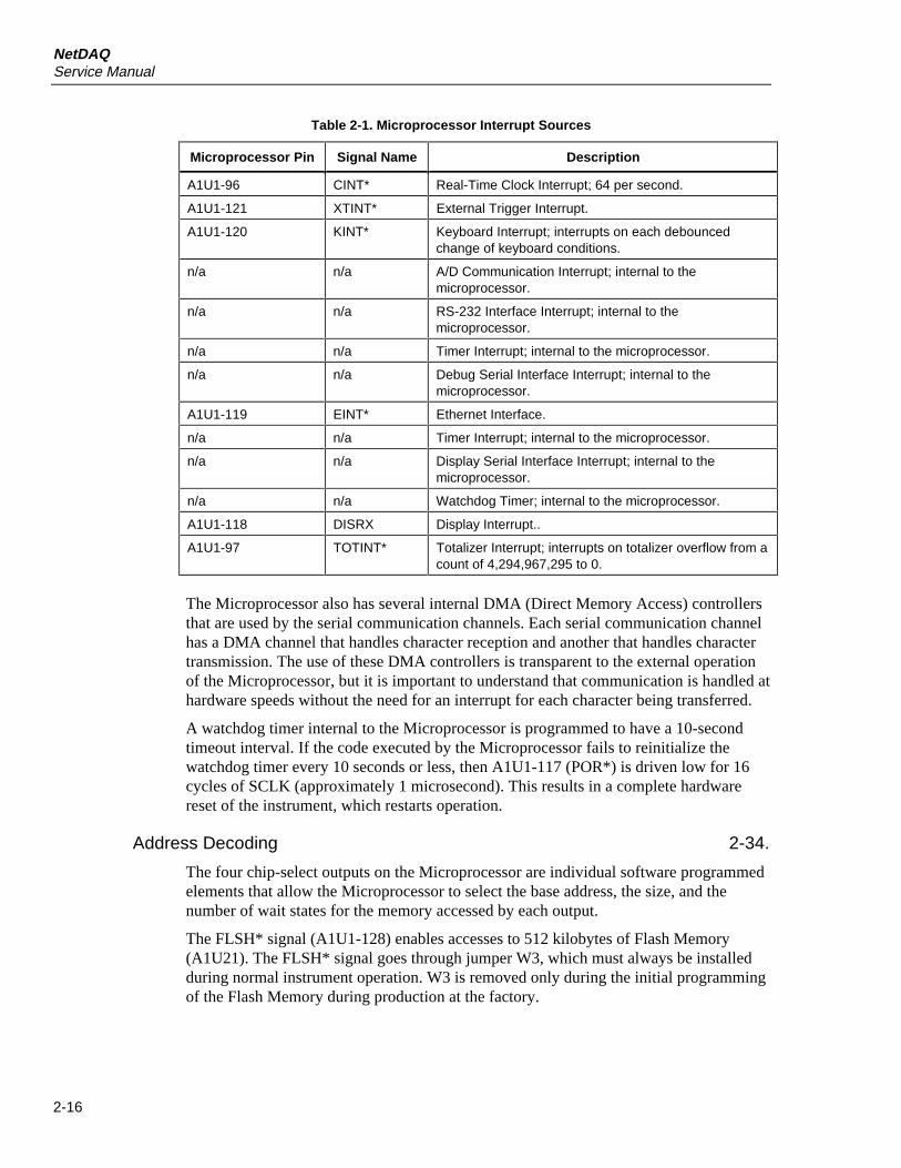
NetDAQService Manual
2-16
Table 2-1. Microprocessor Interrupt Sources
Microprocessor Pin Signal Name Description
A1U1-96 CINT* Real-Time Clock Interrupt; 64 per second.
A1U1-121 XTINT* External Trigger Interrupt.
A1U1-120 KINT* Keyboard Interrupt; interrupts on each debouncedchange of keyboard conditions.
n/a n/a A/D Communication Interrupt; internal to themicroprocessor.
n/a n/a RS-232 Interface Interrupt; internal to themicroprocessor.
n/a n/a Timer Interrupt; internal to the microprocessor.
n/a n/a Debug Serial Interface Interrupt; internal to themicroprocessor.
A1U1-119 EINT* Ethernet Interface.
n/a n/a Timer Interrupt; internal to the microprocessor.
n/a n/a Display Serial Interface Interrupt; internal to themicroprocessor.
n/a n/a Watchdog Timer; internal to the microprocessor.
A1U1-118 DISRX Display Interrupt..
A1U1-97 TOTINT* Totalizer Interrupt; interrupts on totalizer overflow from acount of 4,294,967,295 to 0.
The Microprocessor also has several internal DMA (Direct Memory Access) controllersthat are used by the serial communication channels. Each serial communication channelhas a DMA channel that handles character reception and another that handles charactertransmission. The use of these DMA controllers is transparent to the external operationof the Microprocessor, but it is important to understand that communication is handled athardware speeds without the need for an interrupt for each character being transferred.
A watchdog timer internal to the Microprocessor is programmed to have a 10-secondtimeout interval. If the code executed by the Microprocessor fails to reinitialize thewatchdog timer every 10 seconds or less, then A1U1-117 (POR*) is driven low for 16cycles of SCLK (approximately 1 microsecond). This results in a complete hardwarereset of the instrument, which restarts operation.
Address Decoding 2-34.
The four chip-select outputs on the Microprocessor are individual software programmedelements that allow the Microprocessor to select the base address, the size, and thenumber of wait states for the memory accessed by each output.
The FLSH* signal (A1U1-128) enables accesses to 512 kilobytes of Flash Memory(A1U21). The FLSH* signal goes through jumper W3, which must always be installedduring normal instrument operation. W3 is removed only during the initial programmingof the Flash Memory during production at the factory.
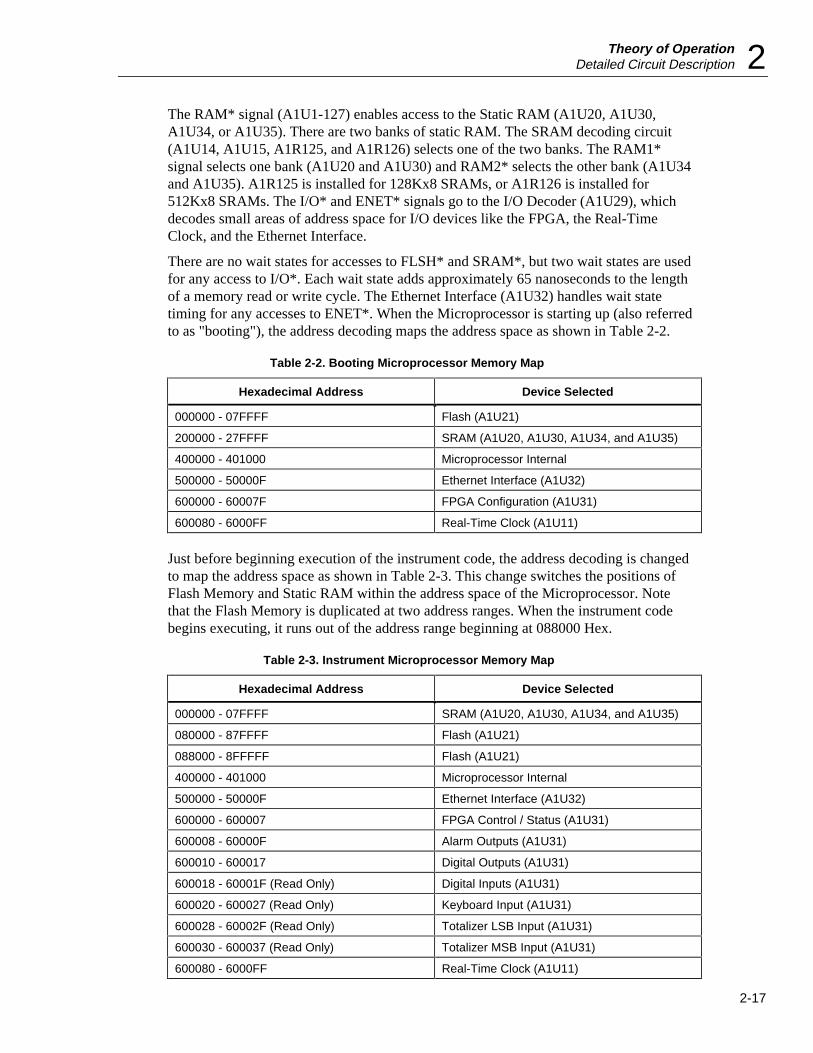
Theory of OperationDetailed Circuit Description 2
2-17
The RAM* signal (A1U1-127) enables access to the Static RAM (A1U20, A1U30,A1U34, or A1U35). There are two banks of static RAM. The SRAM decoding circuit(A1U14, A1U15, A1R125, and A1R126) selects one of the two banks. The RAM1*signal selects one bank (A1U20 and A1U30) and RAM2* selects the other bank (A1U34and A1U35). A1R125 is installed for 128Kx8 SRAMs, or A1R126 is installed for512Kx8 SRAMs. The I/O* and ENET* signals go to the I/O Decoder (A1U29), whichdecodes small areas of address space for I/O devices like the FPGA, the Real-TimeClock, and the Ethernet Interface.
There are no wait states for accesses to FLSH* and SRAM*, but two wait states are usedfor any access to I/O*. Each wait state adds approximately 65 nanoseconds to the lengthof a memory read or write cycle. The Ethernet Interface (A1U32) handles wait statetiming for any accesses to ENET*. When the Microprocessor is starting up (also referredto as "booting"), the address decoding maps the address space as shown in Table 2-2.
Table 2-2. Booting Microprocessor Memory Map
Hexadecimal Address Device Selected
000000 - 07FFFF Flash (A1U21)
200000 - 27FFFF SRAM (A1U20, A1U30, A1U34, and A1U35)
400000 - 401000 Microprocessor Internal
500000 - 50000F Ethernet Interface (A1U32)
600000 - 60007F FPGA Configuration (A1U31)
600080 - 6000FF Real-Time Clock (A1U11)
Just before beginning execution of the instrument code, the address decoding is changedto map the address space as shown in Table 2-3. This change switches the positions ofFlash Memory and Static RAM within the address space of the Microprocessor. Notethat the Flash Memory is duplicated at two address ranges. When the instrument codebegins executing, it runs out of the address range beginning at 088000 Hex.
Table 2-3. Instrument Microprocessor Memory Map
Hexadecimal Address Device Selected
000000 - 07FFFF SRAM (A1U20, A1U30, A1U34, and A1U35)
080000 - 87FFFF Flash (A1U21)
088000 - 8FFFFF Flash (A1U21)
400000 - 401000 Microprocessor Internal
500000 - 50000F Ethernet Interface (A1U32)
600000 - 600007 FPGA Control / Status (A1U31)
600008 - 60000F Alarm Outputs (A1U31)
600010 - 600017 Digital Outputs (A1U31)
600018 - 60001F (Read Only) Digital Inputs (A1U31)
600020 - 600027 (Read Only) Keyboard Input (A1U31)
600028 - 60002F (Read Only) Totalizer LSB Input (A1U31)
600030 - 600037 (Read Only) Totalizer MSB Input (A1U31)
600080 - 6000FF Real-Time Clock (A1U11)
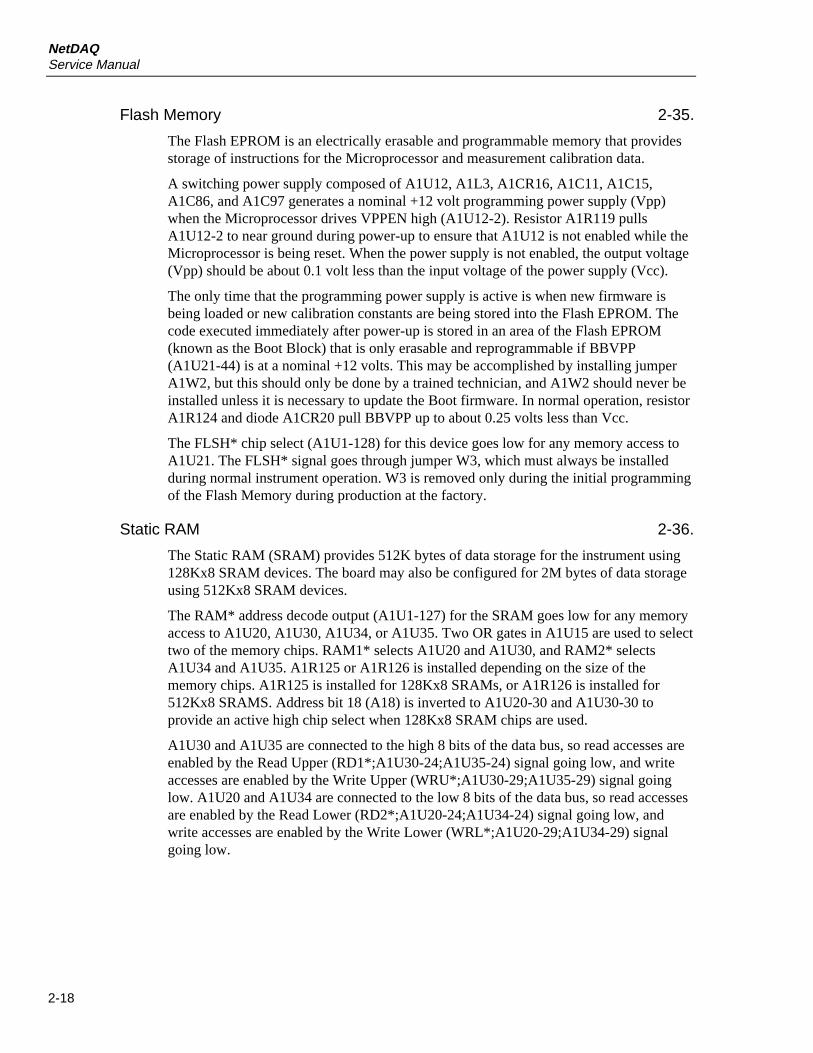
NetDAQService Manual
2-18
Flash Memory 2-35.
The Flash EPROM is an electrically erasable and programmable memory that providesstorage of instructions for the Microprocessor and measurement calibration data.
A switching power supply composed of A1U12, A1L3, A1CR16, A1C11, A1C15,A1C86, and A1C97 generates a nominal +12 volt programming power supply (Vpp)when the Microprocessor drives VPPEN high (A1U12-2). Resistor A1R119 pullsA1U12-2 to near ground during power-up to ensure that A1U12 is not enabled while theMicroprocessor is being reset. When the power supply is not enabled, the output voltage(Vpp) should be about 0.1 volt less than the input voltage of the power supply (Vcc).
The only time that the programming power supply is active is when new firmware isbeing loaded or new calibration constants are being stored into the Flash EPROM. Thecode executed immediately after power-up is stored in an area of the Flash EPROM(known as the Boot Block) that is only erasable and reprogrammable if BBVPP(A1U21-44) is at a nominal +12 volts. This may be accomplished by installing jumperA1W2, but this should only be done by a trained technician, and A1W2 should never beinstalled unless it is necessary to update the Boot firmware. In normal operation, resistorA1R124 and diode A1CR20 pull BBVPP up to about 0.25 volts less than Vcc.
The FLSH* chip select (A1U1-128) for this device goes low for any memory access toA1U21. The FLSH* signal goes through jumper W3, which must always be installedduring normal instrument operation. W3 is removed only during the initial programmingof the Flash Memory during production at the factory.
Static RAM 2-36.
The Static RAM (SRAM) provides 512K bytes of data storage for the instrument using128Kx8 SRAM devices. The board may also be configured for 2M bytes of data storageusing 512Kx8 SRAM devices.
The RAM* address decode output (A1U1-127) for the SRAM goes low for any memoryaccess to A1U20, A1U30, A1U34, or A1U35. Two OR gates in A1U15 are used to selecttwo of the memory chips. RAM1* selects A1U20 and A1U30, and RAM2* selectsA1U34 and A1U35. A1R125 or A1R126 is installed depending on the size of thememory chips. A1R125 is installed for 128Kx8 SRAMs, or A1R126 is installed for512Kx8 SRAMS. Address bit 18 (A18) is inverted to A1U20-30 and A1U30-30 toprovide an active high chip select when 128Kx8 SRAM chips are used.
A1U30 and A1U35 are connected to the high 8 bits of the data bus, so read accesses areenabled by the Read Upper (RD1*;A1U30-24;A1U35-24) signal going low, and writeaccesses are enabled by the Write Upper (WRU*;A1U30-29;A1U35-29) signal goinglow. A1U20 and A1U34 are connected to the low 8 bits of the data bus, so read accessesare enabled by the Read Lower (RD2*;A1U20-24;A1U34-24) signal going low, andwrite accesses are enabled by the Write Lower (WRL*;A1U20-29;A1U34-29) signalgoing low.
Theory of OperationDetailed Circuit Description 2
2-19
Real-Time Clock 2-37.
The Real-Time Clock maintains time and calendar date information for use by theinstrument.
A nonvolatile power supply (Vbb) biases A1U11. The Microprocessor Supervisor(A1U10) monitors the voltage on Vcc (A1U10-2). If Vcc is greater than the voltage ofthe lithium battery (A1U10-8), A1U10 switches Vcc from A1U10-2 to A1U10-1 (Vbb).If Vcc drops below the voltage of the lithium battery (A1U10-8), A1U10 switchesvoltage from lithium battery A1BT1 through current-limiting resistor A1R84 toA1U10-1 (Vbb). The nominal current required from the lithium battery (A1BT1) at roomtemperature with the instrument powered down is approximately 2 microamperes. Thiscan be easily measured by checking the voltage across A1R98.
Memory accesses to the Real-Time Clock (A1U11) are enabled by the RTC addressdecode output (A1U29-16). This signal must go through a NAND gate in A1U36 to theReal-Time Clock chip select input (A1U11-18). This ensures that when the instrument ispowered down and A1U10-7 is driven low, A1U11-18 is driven high so that the contentsof the Real-Time Clock cannot be changed, and the power dissipated by the Real-TimeClock is minimized. A1U11 is connected to the high 8 bits of the data bus, so readaccesses are enabled by the Read Lower (RD1*;A1U11-19) signal going low, and writeaccesses are enabled by the Write Upper (WRU*;A1U11-20) signal going low. Whenthe instrument is powered up, the accuracy of the timebase generated by the internalcrystal may be tested by measuring the frequency of the 1-Hz square wave output(A1U11-4). The Real-Time Clock also has an interrupt output (A1U11-3) that is used bythe Microprocessor to synchronize its internal millisecond timer to the real-time clock.There should be 64 interrupts per second from the real-time clock.
FPGA (Field Programmable Gate Array) 2-38.
When the instrument is powered up, the FPGA, a complex programmable logic device,clears its configuration memory and waits until RESET* (A1U31-78) goes high. TheFPGA then tests its mode pins and should determine that it is in "peripheral"configuration mode (A1U31-54 high; A1U31-52 low; A1U31-56 high). In this mode theMicroprocessor must load the configuration information into the FPGA before the FPGAlogic can begin operation.
The Microprocessor first makes sure that the FPGA is ready to be configured by drivingXD/P* (A1U31-80) low and then pulsing the RESET* (A1U31-78) input low for about10 microseconds. The Microprocessor then waits until the XINIT* (A1U31-65) outputgoes high, indicating that the FPGA has been initialized and is ready for configuration.The Microprocessor then writes a byte of configuration data to the FPGA by drivingPGA* (A1U31-88) low and latching the data on the data inputs (D<0> through D<7>) bypulsing WRL* (A1U31-5) low and then back high. The XRDY (A1U31-99) output thengoes low to indicate that the FPGA is busy loading that configuration byte. TheMicroprocessor then waits until XRDY goes high again before loading the nextconfiguration byte, and the sequence is repeated until the last byte is loaded. While theconfiguration data is being loaded, the FPGA drives the XD/P* signal (A1U31-80) low.When the FPGA has been completely configured, the XD/P* signal is released andpulled high by resistor A1R64. The Microprocessor repeats the configuration sequence ifXD/P* (A1U31-80) does not go high when it is expected to.
NetDAQService Manual
2-20
The FPGA contains the following eight functional elements after the Microprocessor hasloaded the configuration into the FPGA:
• Clock Dividers
• Internal Register Address Decoding
• Keyboard Scanner
• Digital I/O Buffers
• Latches
• Totalizer Debouncing and Mode Selection
• Totalizer Counter
• External Trigger Logic
Clock Dividers The 15.36-MHz system clock (A1U31-30) is divided down by theClock Dividers to create the 1.024-MHz Display Clock (DCLK; A1U31-19). TheDisplay Clock is not a square wave; it is low for 2/3 of a cycle and high for the other 1/3.The Display Clock is also used internal to the FPGA to create the 128-kHz TotalizerDebouncer Clock and the 4-kHz Keyboard Scanner Clock.
Internal Register Address Decoding The FPGA logic decodes four bits of the addressbus (A<3> through A<6>), the PGA* chip select signal (A1U31-88), RD2* (A1U31-95),and WRL* (A1U31-5) to allow the Microprocessor to read five registers and write tothree registers implemented in the FPGA logic. The absolute addresses are listed inTable 2-3.
Keyboard Scanner The Keyboard Scanner sequences through the array of switches onthe Display Assembly to detect and debounce switch closures. After a switch closure isdetected, it must remain closed for at least 16 milliseconds before the Microprocessor isinterrupted and the Keyboard Input register is read from the FPGA. When the keyboardinterrupt (KINT*, A1U31-62) goes low, the Keyboard Scanner stops scanning until theMicroprocessor reads the Keyboard Input register, which automatically clears theinterrupt by driving KINT* high again. The FPGA interrupts the Microprocessor againwhen the switch on the Display Assembly is detected as open again. Actually theMicroprocessor is interrupted once for each debounced change in the contents of theKeyboard Input register. See also the information on "Front Panel Switches" in the"Display PCA" section for this instrument.
The Microprocessor can enable or disable the Keyboard Scanner by changing the state ofa bit in the Control/Status register that is in the FPGA. The Keyboard Scanner is disabledif the instrument is in either the RWLS or LWLS state (see Users Manual; RWLS, andLWLS Computer Interface Commands).
Digital I/O Buffers and Latches The FPGA logic implements internal registers for theeight Digital Outputs (DO<0> through DO<7>), Master Alarm Output (AO<2>), andTrigger Output (AO<3>). The two Alarm Outputs (AO<0> and ADO<1>) are notsupported. These registers are both written and read by the Microprocessor. The FPGAlogic also implements an eight-bit input buffer so that the Microprocessor can read theeight Digital Input lines (DI<0> through DI<7>). See also "Digital Input Buffers" and"Digital and Alarm Output Drivers."
Theory of OperationDetailed Circuit Description 2
2-21
Totalizer Debouncing and Mode Selection Logic internal to the FPGA lets theMicroprocessor enable a debouncer in the Totalizer input signal path. You can find thedetailed description of the Totalizer Debouncer and Mode Selection later in this chapterunder the heading "Totalizer Input."
Totalizer Counter There is a 16 bit counter internal to the FPGA to count the totalizerinputs. When the 16 bit counter overflows, the microprocessor is interrupted and asoftware counter is incremented.
External Trigger Logic Logic internal to the FPGA allows the Microprocessor to setup the External Trigger Logic to interrupt on rising or falling edges of the XTI input tothe FPGA. The FPGA also allows the Microprocessor to pulse an external trigger outputfrom the FPGA. The detailed description of the External Trigger operation may be foundlater in this chapter in the "External Trigger Circuits" section.
Serial Communication (Guard Crossing) 2-39.
The transmission of information from the Microprocessor (A1U1) to the A/DMicroprocessor (A3U5) is accomplished via the circuit made up of A1U5, A1R8,A1R16, and A1CR22. The transmit output from the Microprocessor (A1U1-80) switchescurrent through optocoupler LED (A1U5-3). Resistor A1R8 limits the current throughthe LED.
The photodiode in A1U5 responds to the light emitted by the LED when A1U1-80 isdriven low. The open collector output (A1U5-6) is pulled high by A1R16 and A1CR22.This output is connected to a serial port input on the A/D Microprocessor (A3U5-53).
The transmission of data from the A/D Microprocessor (A3U5) to the Microprocessor(A1U1) is accomplished via the circuit made up of A1U7, A1R7, and A1R3. Thetransmit output from the A/D Microprocessor (A3U5-54) drives the optocoupler LED(A1U7-3). The current through the LED is limited by resistor A1R7. The photodiode inA1U7 responds to the light emitted by the LED when A1U7-3 is driven low.
The photodiode in A1U7 responds to the light emitted by the LED when A3U5-54 isdriven low. The open collector output (A1U7-6) is pulled high by A1R3. This output isconnected to a serial port input on the Microprocessor (A1U1-52).
RS-232 Interface 2-40.
The RS-232 interface is composed of connector A1J4, RS-232 Driver/Receiver A1U13,and the serial communication hardware in Microprocessor A1U1.
The serial communication transmit signal (A1U1-54) goes to the RS-232 driver(A1U13-14), where it is inverted and level shifted so that the RS-232 transmit signaltransitions between approximately +5.0 and -5.0V dc. When the instrument is nottransmitting, the driver output (TP13;A1U13-3) is approximately -5.0V dc. The RS-232receive signal from A1J4 goes to the RS-232 receiver A1U13-4, which inverts and levelshifts the signal so that the input to the serial communication hardware transitionsbetween 0 and +5.0V dc. When nothing is being transmitted to the instrument, thereceiver output (TP12;A1U13-13) is +5.0V dc.
NetDAQService Manual
2-22
Data Terminal Ready (DTR) and Request To Send (RTS) are modem control signalscontrolled by the Microprocessor. When the instrument is powered up, theMicroprocessor initially sets DTR and RTS false by setting A1U1-61 and A1U1-59 high,which results in the RS-232 driver outputs (A1U13-7 and A1U13-5 respectively) goingto -5.0V dc. When the instrument has initialized the RS-232 interface and is ready toreceive and transmit, A1U1-61 and A1U1-59 goes low, resulting in the RS-232 DTR andRTS signals going to +5.0V dc. The RS-232 DTR and RTS signals remain at +5.0V dcuntil the instrument is powered down except for a short period of time when the userchanges RS-232 communication parameters from the front panel of the instrument.
Clear To Send (CTS) and Data Set Ready (DSR) are modem control inputs from theconnected RS-232 equipment. Of these signals, only CTS is used when CTS flow controlis enabled via the RS-232 communication setup menu. The CTS modem control signalfrom A1J4 goes to the RS-232 receiver A1U13-6, which inverts and level shifts thesignal so that the input to the Microprocessor (A1U1-58) transitions between 0 and+5.0V dc. When the instrument is cleared to send characters to the RS-232 interface, thereceiver output (A1U13-11) is +5.0V dc. If the RS-232 CTS signal is not driven by theattached RS-232 equipment, the receiver output (A1U13-11) is near 0V dc.
Ethernet Interface 2-41.
The Ethernet Interface is the primary means the instrument uses to communicate with ahost computer. The interface is comprised of an Ethernet chip, a buffer memory, twophysical connectors, and electrically isolated interfaces between the Ethernet chip andthe connectors. Only one of the two connectors are used at a time.
Ethernet Chip and Buffer Memory The Ethernet chip (A1U32) is directly connectedto the Microprocessor’s address and data bus. Three address lines are used to selectregisters within the Ethernet Chip, and data is transferred over 16 data lines. The chipselect is performed by read and write strobe signals EIOR* and EIOW* (A1U32-154 andA1U32-155). EIOR* is driven low when the Microprocessor is reading from theEthernet Chip, and EIOW* is driven low when the Microprocessor is writing to theEthernet Chip. The Ethernet chip signals the end of a read or write cycle by driving itsRDY output (A1U32-151) low. This enables the output of tri-state buffer A1U2-3,driving the DTACK* signal low to the Microprocessor (A1U1-85). When theMicroprocessor sees DTACK* go low, it ends the read or write cycle to the Ethernetchip. The Ethernet Chip may also interrupt the Microprocessor by driving EINT* low(A1U32-133.) A1R133 is used to pull EINT* high.
Unlike RS-232 and other serial interfaces, Ethernet transfers data as packets of several Kbytes of data, instead of as single bytes. The buffer memory is used to store packetswhile they are being received, or while being transmitted. The Ethernet Chip (A1U32) isconnected directly to the buffer memory (A1U33). Packets being received or transmittedare stored to or retrieved from the buffer memory by the Ethernet Chip. The buffermemory (A1U33) provides 32K bytes of storage for data packets.
Packets stored in the buffer memory (A1U33) are transferred to or from the Static RAM(A1U20, A1U30, A1U34, or A1U35) by a DMA controller in the Microprocessor(A1U1). This transfer is done with read or write cycles to the Ethernet Chip (A1U32).
Theory of OperationDetailed Circuit Description 2
2-23
The clock for the Ethernet Chip is provided by A1Y2, A1C38, and A1C89, which areconnected directly to A1U32-17 and A1U32-18. This provides a 20 MHz clock to theEthernet Chip. The clock allows the Ethernet Interface to send and receive data at10 M-bits per second.
A1R107 sets internal bias currents in the Ethernet Chip (A1U32). The voltage dropacross this resistor is normally around 1.25 volts.
The Ethernet Chip also drives three LEDs. A1DS2 indicates that a packet is beingreceived. A1DS3 indicates that the Ethernet Chip is transmitting a packet. A1DS1indicates two different things depending on the type of physical interface being used. If10BASE-2 (Coax) is being used, A1DS1 indicates when collisions were detected on theEthernet. If 10BASE-T (Twisted Pair) is being used, A1DS1 indicates whether the linkto the host computer is intact. A1DS1 is driven by the Ethernet Chip (A1U32) through adual diode (A1CR4), which ORs together two outputs (A1U32-59 and A1U32-60).A1DS2 and A1DS3 are driven directly by A1U32-57 and A1U32-58. Resistors A1R37,A1R122, and A1R121 limit current to LEDs A1DS1, A1DS2, and A1DS3.
Ethernet Connectors The instrument is connected to the Ethernet by either a10BASE-2 interface (A1P2) or a 10BASE-T interface (A1P1). 10BASE-2 uses coaxialcable to attach instrument to a host computer. Other instruments and possibly otherequipment may be attached to the same coaxial cable when a 10BASE-2 interface isused. 10BASE-T uses twisted pair cable to attach instrument to some kind of hub. A hostcomputer, other instruments, and other equipment are connected to a 10BASE-T hubusing separate twisted pair cables.
10BASE-T Ethernet Connector Pulse transformer A1T4 provides electrical isolationbetween the Ethernet Chip (A1U32) and the 10BASE-T connector (A1P1). Two twistedpairs are used in a 10BASE-T cable. One pair is used to transmit data (A1P1-1 andA1P1-2), and the other is used to receive data (A1P1-3 and A1P1-6). Resistors A1R86,A1R95, and capacitor A1C60 provide a termination network for data received throughthe pulse transformer (A1T4). Resistors A1R32, A1R76, A1R92, A1R100, and A1R120provide a termination network for data transmitted through the pulse transformer(A1T4). Connector A1P1 provides chassis potential on pins 9 and 10 to shield the cableand provide a system ground. Capacitor A1C28 helps the instrument meet EMIrequirements.
10BASE2 Ethernet Connector Ethernet transceiver chip A1U16 drives and receives dataon the 10BASE-2 (Coaxial) interface connector (A1P2). In addition, A1U16 detectscollisions on the Ethernet. Data and collision detect signals are transferred between thetransceiver chip (A1U16) and the Ethernet Interface (A1U32) through pulse transformerA1T3. Power supply module A1U38 provides a -9V isolated power supply to the10BASE-2 transceiver chip A1U16. The power supply module can be powered down bya signal from the Ethernet Chip (A1U32-64) when the 10BASE-2 interface is not beingused. The transceiver chip (A1U16) is protected from electrostatic discharge (ESD) byresistors A1R136, A1R77, capacitors A1C23, A1C61, and MOV A1RV2. A1R18 setsinternal bias currents in A1U16.
NetDAQService Manual
2-24
Pulse transformer A1T3 provides electrical isolation between the Ethernet Chip (A1U32)and the 10BASE-2 transceiver chip (A1U16). Data is transmitted from the Ethernet Chip(A1U32) to the transceiver chip (A1U16) through pins 1, 2, 15, and 16 of pulsetransformer A1T3. Resistor A1R24 terminates the outputs from the Ethernet Chip(A1U32). Data is received from the transceiver chip (A1U16) through pins 4, 5, 12, and13 of pulse transformer A1T3. Resistors A1R42, A1R65, and capacitor A1C33 provide atermination network for data received through the pulse transformer (A1T4). Thetransceiver chip indicates a collision was detected on the Ethernet through pins 7, 8, 9,and 10 of pulse transformer A1T3. Resistors A1R85, A1R87, and capacitor A1C69provide a termination network for the collision detected signal received through thepulse transformer (A1T4).
Digital Inputs and Outputs 2-42.
The following paragraphs describe the digital input/output as follows:
• Digital Input Threshold
• Digital Input Buffers
• Digital and Alarm Output Drivers
• Totalizer Input
• External Trigger Circuits
Digital Input Threshold 2-43.
The Digital Input Threshold circuit sets the input threshold level for the Digital InputBuffers and the Totalizer Input. A fixed value voltage divider (A1R36, A1R37) and aunity gain buffer amplifier (A1U8) are the main components in this circuit. The voltagefrom the divider (approximately +1.4V dc) is then buffered by A1U8, which sets theinput threshold. Capacitor A1C29 filters the divider voltage at the input of A1U8.
Digital Input Buffers 2-44.
Since the eight Digital Input Buffers are identical in design, only components used forDigital Input 0 are referenced in this description. If the Digital Output Driver(A1U17-12) is off, the input to the Digital Input Buffer is determined by the voltagelevel at A1J5-10. If the Digital Output Driver is on, the input of the Digital Input Bufferis the voltage at the output of the Digital Output Driver.
The Digital Input Threshold circuit and resistor network A1Z1 determine the inputthreshold voltage and Hysteresis for inverting comparator A1U3. The inverting input ofthe comparator (A1U3-2) is protected by a series resistor (A1Z3) and diode A1CR14. Anegative input clamp circuit (A1Q9, A1Z2, and A1CR17) sets a clamp voltage ofapproximately +0.7V dc for the protection diodes of all Digital Input Buffers. A negativeinput voltage at A1J5-10 causes A1CR14 to conduct current, clamping the comparatorinput A1U3-2 at approximately 0V dc.
The input threshold of +1.4V dc and a hysteresis of +0.5V dc are used for all DigitalInput Buffers. When the input of the Digital Input Buffer is greater than approximately+1.65V dc, the output of the inverting comparator is low. When the input then dropsbelow about +1.15V dc, the output of the inverting comparator goes high.
Theory of OperationDetailed Circuit Description 2
2-25
Digital and Alarm Output Drivers 2-45.
Since the 11 Digital Output and Alarm Output Drivers are identical in design, thefollowing example description references only the components that are used for theMaster Alarm Output (AO<2>).
The Microprocessor controls the state of the Master Alarm Output Driver by writing tothe Alarm Output register in the FPGA (A1U31) to set the level of output A1U31-61.When A1U31-61 is set high, the output of the open-collector Darlington driver(A1U17-14) sinks current through current-limiting resistor A1R60. When A1U31-61 isset low, the driver output turns off and is pulled up by A1Z2 and/or the voltage of theexternal device that the output is driving. If the driver output is driving an externalinductive load, the internal flyback diode (A1U17-9) conducts the energy into MOVA1RV1 to keep the driver output from being damaged by excessive voltage. CapacitorA1C56 ensures that the instrument meets electromagnetic interference (EMI) andelectromagnetic compatibility (EMC) performance requirements.
Totalizer Input 2-46.
The Totalizer Input circuit consists of Input Protection, a Digital Input Buffer circuit,and a Totalizer Debouncing circuit. The Digital Input Buffer for the totalizer is protectedfrom electrostatic discharge (ESD) damage by A1R49 and A1C43. Refer to the detaileddescription of the Digital Input Buffer circuit for more information.
The Totalizer Debounce circuit in the FPGA (A1U31) allows the Microprocessor toselect totalizing of either the input signal or the debounced input signal. The bufferedTotalizer Input signal (TOTI*) goes into the FPGA at A1U31-12. Inside the FPGA, thetotalizer signal is routed to a 16-bit counter in the FPGA. The counter can be read at anytime by the microprocessor. When the 16-bit counter overflows, the microprocessor isinterrupted by the Totalizer Interrupt signal (TOTINT*) that comes from A1U31-8. Themicroprocessor uses this interrupt (A1U1-97) to increment a software counter.
The actual debouncing of the input signal is accomplished by A1U31. Counters dividethe 15.36-MHz system clock down to 128 kHz for the debouncing circuit. An EXORgate compares the input signal (TOTI*) and the latched output of the debouncer. If thesesignals differ, the EXOR gate output goes high, enabling the debouncer. If the inputremains stable for 1.75 milliseconds, the debouncer output changes state. If the inputdoes not remain stable for 1.75 milliseconds, the debouncer output does not change state.If the Microprocessor selected totalizing of the debounced input signal, the debounceroutput is connected to the 16-bit counter inside the FPGA.
External Trigger Circuits 2-47.
The External Trigger Input circuit can be configured by the Microprocessor to interrupton a rising or falling edge of the TGIN* input (A1J6-2) or to not interrupt on anytransitions of the TGIN* input. The falling edge of the TGIN* input is used by theinstrument firmware as an indication to start scanning, and the rising edge is used as anindication to stop scanning.
The External Trigger Input is pulled up to +5V dc by A1Z2 and is protected fromelectrostatic discharge (ESD) damage by A1R58, A1C54, A1Z3, and A1CR15. CapacitorA1C54 helps ensure that the instrument meets EMI/EMC performance requirements.
NetDAQService Manual
2-26
The input (XTI) is then routed to the FPGA (A1U31), that contains the External Triggercontrol circuitry. The Microprocessor sets control register bits in the FPGA (A1U31) tocontrol the external trigger circuit. The External Trigger control circuit output(A1U31-9) drives an interrupt input on the Microprocessor (A1U1-121).
If External Triggering is enabled (see User Manual), the Microprocessor sets FPGAcontrol register bits to allow a low level on the TGIN* input to cause the ExternalTrigger Interrupt (XTINT*; A1U31-9) to go low. The Microprocessor then changes theFPGA control register bits to allow a high level on the TGIN* input to cause XTINT*(A1U31-9) to go low. Thus the Microprocessor can detect both rising and falling edgeson the TGIN* input. Normally, the XTINT* output of the FPGA (A1U31-9) should below only for a few microseconds at any time. If it is held low constantly, the instrumentdoes not operate. Resistor A1R39 pulls the XTINT* output high to ensure that it is highduring power-up.
The instrument has a trigger output line that is pulsed low when the Microprocessorwrites a bit to a register in the FPGA (A1U31). The trigger output line (TGOUT*A1J6-3) is pulsed low for 250 to 500 microseconds at the beginning of the firstmeasurement of each acquisition scan. The pulse width is set by circuitry within theFPGA. The output circuitry for the trigger output is the same as for the digital and alarmoutput buffers, except for transistor A1Q10. This transistor is used to increase theamount of current the trigger output can sink. This allows the trigger output to drive thetrigger inputs of up to 19 instruments.
A2 Display PCA Circuit Description 2-48.
Display Assembly operation is classified into six functional circuit blocks as follows:
• Main PCA Connector
• Front Panel Switches
• Display
• Beeper Drive Circuit
• Watchdog Timer/Reset Circuit
• Display Controller
Each circuit block is described in the following paragraphs.
Main PCA Connector 2-49.
The 20-pin Main PCA Connector (A2J1) provides the interface between the Main PCAand the other functional blocks on the Display PCA. Seven of the connector pins providethe necessary connections to the four power supply voltages: -30V dc, -5V dc (Vee),+4.9V dc (Vcc), and 5.4V ac filament voltage (see Table 2-4). Six pins are used toprovide the interface to the Front Panel Switches (A2SWR1 through A2SWR6). Theother seven signals interface the Microprocessor (A1U4) to the Display Controller(A2U1) and pass the reset signals between the assemblies.
Theory of OperationDetailed Circuit Description 2
2-27
Table 2-4. A2 Display Power Supply Connections
Power Supply A2J1 Pins Nominal Voltage
Vcc 8 +4.9V dc
Vee 6 -5.0V dc
Vload 7 -30V dc
FIL1/FIL2 2/3 5.4V ac
Front Panel Switches 2-50.
The FPGA monitors the front panel switches (see below) using six interface signalsSWR1 through SWR6. The ground connection is already available from the powersupply.
Switch Designation Switch Function
S11 COMM
S12 Left Arrow
S13 DIO
S14 Right Arrow
S15 MON
S16 ENTER
S17 Up Arrow
S18 Down Arrow
S21 CAL Enable
The six Switch Interface Signals (SWR1 though SWR6) are connected to bidirectionalI/O pins on the FPGA. Each successive column has one less switch. This arrangementallows the unused interface signals to function as strobe signals when their respectivecolumn is driven by the FPGA. The FPGA cycles through six steps to scan the completefront panel switch matrix. Table 2-5 shows the interface signal state and, if the signalstate is an output, the switches that may be detected as closed.
In step 1, six I/O pins are set to input, and the interface signal values are read. In steps 2through 6, the pin listed as O is set to output zero, the other pins are read, and pinsindicated by a Z are ignored.
Each of the interface signals is pulled up to the +5V dc supply by a 10 kΩ resistor innetwork A2Z1. Normally, the resistance between any two of the interface signals isapproximately 20 kΩ. Checking resistances between any two signals (SWR1 throughSWR6) verifies proper termination by resistor network A2Z1.
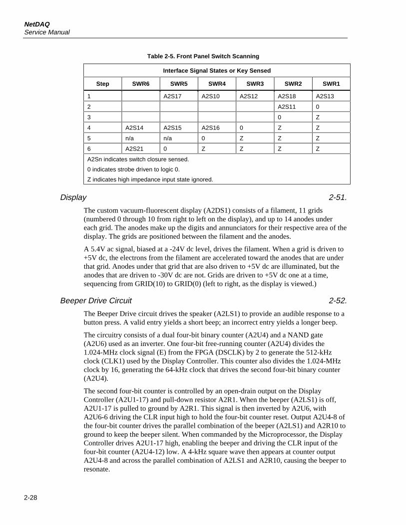
NetDAQService Manual
2-28
Table 2-5. Front Panel Switch Scanning
Interface Signal States or Key Sensed
Step SWR6 SWR5 SWR4 SWR3 SWR2 SWR1
1 A2S17 A2S10 A2S12 A2S18 A2S13
2 A2S11 0
3 0 Z
4 A2S14 A2S15 A2S16 0 Z Z
5 n/a n/a 0 Z Z Z
6 A2S21 0 Z Z Z Z
A2Sn indicates switch closure sensed.
0 indicates strobe driven to logic 0.
Z indicates high impedance input state ignored.
Display 2-51.
The custom vacuum-fluorescent display (A2DS1) consists of a filament, 11 grids(numbered 0 through 10 from right to left on the display), and up to 14 anodes undereach grid. The anodes make up the digits and annunciators for their respective area of thedisplay. The grids are positioned between the filament and the anodes.
A 5.4V ac signal, biased at a -24V dc level, drives the filament. When a grid is driven to+5V dc, the electrons from the filament are accelerated toward the anodes that are underthat grid. Anodes under that grid that are also driven to +5V dc are illuminated, but theanodes that are driven to -30V dc are not. Grids are driven to +5V dc one at a time,sequencing from GRID(10) to GRID(0) (left to right, as the display is viewed.)
Beeper Drive Circuit 2-52.
The Beeper Drive circuit drives the speaker (A2LS1) to provide an audible response to abutton press. A valid entry yields a short beep; an incorrect entry yields a longer beep.
The circuitry consists of a dual four-bit binary counter (A2U4) and a NAND gate(A2U6) used as an inverter. One four-bit free-running counter (A2U4) divides the1.024-MHz clock signal (E) from the FPGA (DSCLK) by 2 to generate the 512-kHzclock (CLK1) used by the Display Controller. This counter also divides the 1.024-MHzclock by 16, generating the 64-kHz clock that drives the second four-bit binary counter(A2U4).
The second four-bit counter is controlled by an open-drain output on the DisplayController (A2U1-17) and pull-down resistor A2R1. When the beeper (A2LS1) is off,A2U1-17 is pulled to ground by A2R1. This signal is then inverted by A2U6, withA2U6-6 driving the CLR input high to hold the four-bit counter reset. Output A2U4-8 ofthe four-bit counter drives the parallel combination of the beeper (A2LS1) and A2R10 toground to keep the beeper silent. When commanded by the Microprocessor, the DisplayController drives A2U1-17 high, enabling the beeper and driving the CLR input of thefour-bit counter (A2U4-12) low. A 4-kHz square wave then appears at counter outputA2U4-8 and across the parallel combination of A2LS1 and A2R10, causing the beeper toresonate.
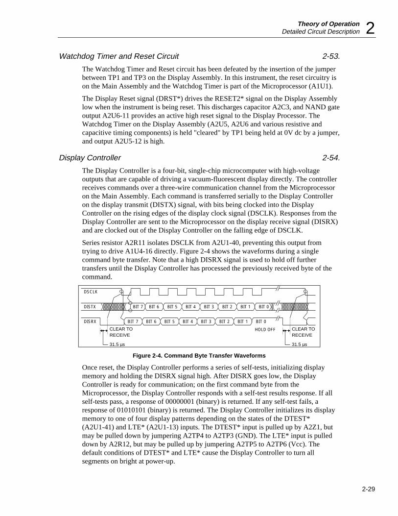
Theory of OperationDetailed Circuit Description 2
2-29
Watchdog Timer and Reset Circuit 2-53.
The Watchdog Timer and Reset circuit has been defeated by the insertion of the jumperbetween TP1 and TP3 on the Display Assembly. In this instrument, the reset circuitry ison the Main Assembly and the Watchdog Timer is part of the Microprocessor (A1U1).
The Display Reset signal (DRST*) drives the RESET2* signal on the Display Assemblylow when the instrument is being reset. This discharges capacitor A2C3, and NAND gateoutput A2U6-11 provides an active high reset signal to the Display Processor. TheWatchdog Timer on the Display Assembly (A2U5, A2U6 and various resistive andcapacitive timing components) is held "cleared" by TP1 being held at 0V dc by a jumper,and output A2U5-12 is high.
Display Controller 2-54.
The Display Controller is a four-bit, single-chip microcomputer with high-voltageoutputs that are capable of driving a vacuum-fluorescent display directly. The controllerreceives commands over a three-wire communication channel from the Microprocessoron the Main Assembly. Each command is transferred serially to the Display Controlleron the display transmit (DISTX) signal, with bits being clocked into the DisplayController on the rising edges of the display clock signal (DSCLK). Responses from theDisplay Controller are sent to the Microprocessor on the display receive signal (DISRX)and are clocked out of the Display Controller on the falling edge of DSCLK.
Series resistor A2R11 isolates DSCLK from A2U1-40, preventing this output fromtrying to drive A1U4-16 directly. Figure 2-4 shows the waveforms during a singlecommand byte transfer. Note that a high DISRX signal is used to hold off furthertransfers until the Display Controller has processed the previously received byte of thecommand.
BIT 7
BIT 7
HOLD OFF CLEAR TORECEIVE
31.5 µs
DISTX
DSCLK
DISRX
CLEAR TORECEIVE
31.5 µs
BIT 6 BIT 5 BIT 4 BIT 3 BIT 2 BIT 1 BIT 0
BIT 6 BIT 5 BIT 4 BIT 3 BIT 2 BIT 1 BIT 0
Figure 2-4. Command Byte Transfer Waveforms
Once reset, the Display Controller performs a series of self-tests, initializing displaymemory and holding the DISRX signal high. After DISRX goes low, the DisplayController is ready for communication; on the first command byte from theMicroprocessor, the Display Controller responds with a self-test results response. If allself-tests pass, a response of 00000001 (binary) is returned. If any self-test fails, aresponse of 01010101 (binary) is returned. The Display Controller initializes its displaymemory to one of four display patterns depending on the states of the DTEST*(A2U1-41) and LTE* (A2U1-13) inputs. The DTEST* input is pulled up by A2Z1, butmay be pulled down by jumpering A2TP4 to A2TP3 (GND). The LTE* input is pulleddown by A2R12, but may be pulled up by jumpering A2TP5 to A2TP6 (Vcc). Thedefault conditions of DTEST* and LTE* cause the Display Controller to turn allsegments on bright at power-up.
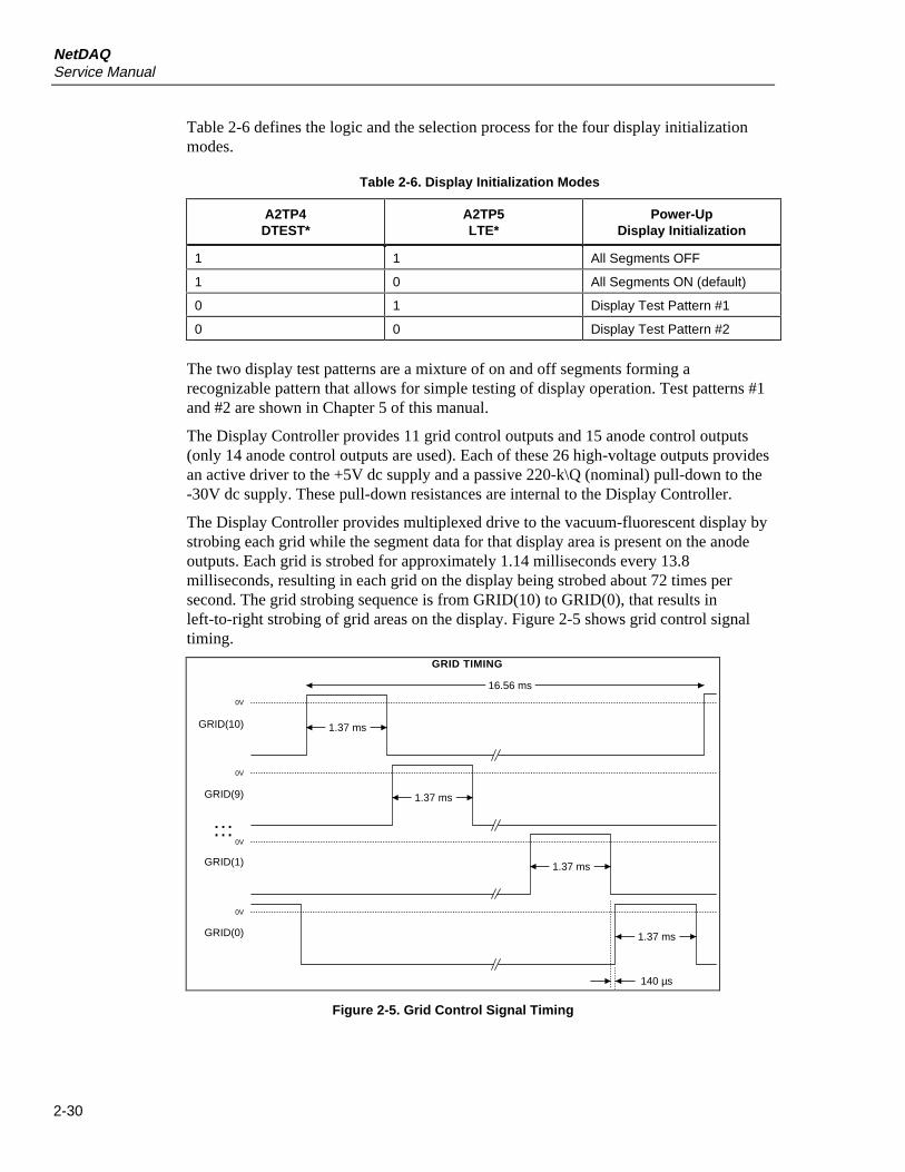
NetDAQService Manual
2-30
Table 2-6 defines the logic and the selection process for the four display initializationmodes.
Table 2-6. Display Initialization Modes
A2TP4DTEST*
A2TP5LTE*
Power-UpDisplay Initialization
1 1 All Segments OFF
1 0 All Segments ON (default)
0 1 Display Test Pattern #1
0 0 Display Test Pattern #2
The two display test patterns are a mixture of on and off segments forming arecognizable pattern that allows for simple testing of display operation. Test patterns #1and #2 are shown in Chapter 5 of this manual.
The Display Controller provides 11 grid control outputs and 15 anode control outputs(only 14 anode control outputs are used). Each of these 26 high-voltage outputs providesan active driver to the +5V dc supply and a passive 220-k\Q (nominal) pull-down to the-30V dc supply. These pull-down resistances are internal to the Display Controller.
The Display Controller provides multiplexed drive to the vacuum-fluorescent display bystrobing each grid while the segment data for that display area is present on the anodeoutputs. Each grid is strobed for approximately 1.14 milliseconds every 13.8milliseconds, resulting in each grid on the display being strobed about 72 times persecond. The grid strobing sequence is from GRID(10) to GRID(0), that results inleft-to-right strobing of grid areas on the display. Figure 2-5 shows grid control signaltiming.
1.37 ms
1.37 ms
1.37 ms
1.37 ms
16.56 ms
0V
GRID(10)
0V
GRID(9)
0V
GRID(1)
0V
GRID(0)
……
140 µs
GRID TIMING
Figure 2-5. Grid Control Signal Timing
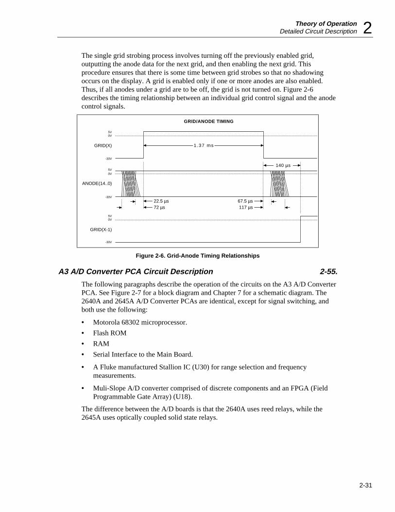
Theory of OperationDetailed Circuit Description 2
2-31
The single grid strobing process involves turning off the previously enabled grid,outputting the anode data for the next grid, and then enabling the next grid. Thisprocedure ensures that there is some time between grid strobes so that no shadowingoccurs on the display. A grid is enabled only if one or more anodes are also enabled.Thus, if all anodes under a grid are to be off, the grid is not turned on. Figure 2-6describes the timing relationship between an individual grid control signal and the anodecontrol signals.
1.37 ms
0V
5V
ANODE(14..0)
-30V
GRID(X)
-30V
GRID(X-1)
GRID/ANODE TIMING
5V
-30V
72 µs22.5 µs
117 µs67.5 µs
140 µs
0V5V
0V
Figure 2-6. Grid-Anode Timing Relationships
A3 A/D Converter PCA Circuit Description 2-55.
The following paragraphs describe the operation of the circuits on the A3 A/D ConverterPCA. See Figure 2-7 for a block diagram and Chapter 7 for a schematic diagram. The2640A and 2645A A/D Converter PCAs are identical, except for signal switching, andboth use the following:
• Motorola 68302 microprocessor.
• Flash ROM
• RAM
• Serial Interface to the Main Board.
• A Fluke manufactured Stallion IC (U30) for range selection and frequencymeasurements.
• Muli-Slope A/D converter comprised of discrete components and an FPGA (FieldProgrammable Gate Array) (U18).
The difference between the A/D boards is that the 2640A uses reed relays, while the2645A uses optically coupled solid state relays.
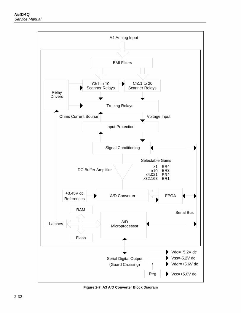
NetDAQService Manual
2-32
A4 Analog Input
EMI Filters
Ch1 to 10Scanner Relays
Ch11 to 20Scanner Relays
Treeing Relays
Voltage InputOhms Current Source
Input Protection
Signal Conditioning
Selectable Gains
x1x10
x4.021x32.168
BR4BR3BR2BR1
A/D Converter+3.45V dc
ReferencesFPGA
Microprocessor
(Guard Crossing)
Serial Bus
Flash
RAM
Serial Digital Output
RelayDrivers
Latches
Vdd=+5.2V dc
Vss=-5.2V dc
Vddr=+5.6V dc
Reg Vcc=+5.0V dc
A/D
DC Buffer Amplifier
Figure 2-7. A3 A/D Converter Block Diagram
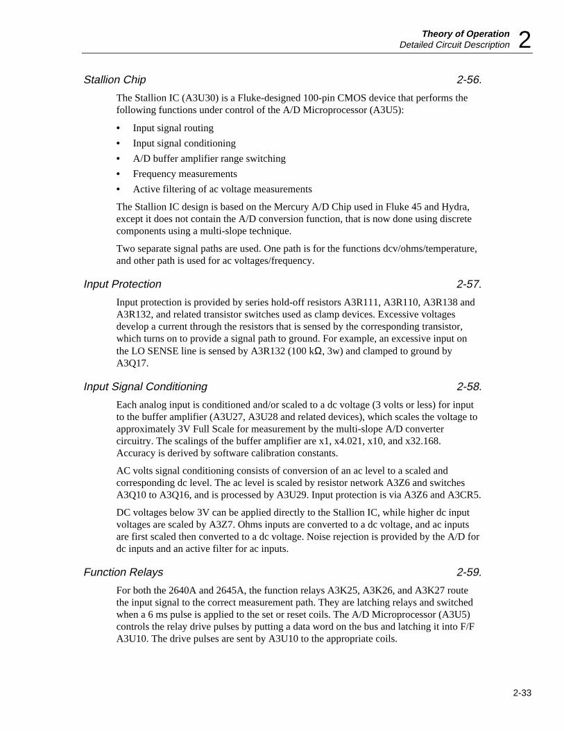
Theory of OperationDetailed Circuit Description 2
2-33
Stallion Chip 2-56.
The Stallion IC (A3U30) is a Fluke-designed 100-pin CMOS device that performs thefollowing functions under control of the A/D Microprocessor (A3U5):
• Input signal routing
• Input signal conditioning
• A/D buffer amplifier range switching
• Frequency measurements
• Active filtering of ac voltage measurements
The Stallion IC design is based on the Mercury A/D Chip used in Fluke 45 and Hydra,except it does not contain the A/D conversion function, that is now done using discretecomponents using a multi-slope technique.
Two separate signal paths are used. One path is for the functions dcv/ohms/temperature,and other path is used for ac voltages/frequency.
Input Protection 2-57.
Input protection is provided by series hold-off resistors A3R111, A3R110, A3R138 andA3R132, and related transistor switches used as clamp devices. Excessive voltagesdevelop a current through the resistors that is sensed by the corresponding transistor,which turns on to provide a signal path to ground. For example, an excessive input onthe LO SENSE line is sensed by A3R132 (100 kΩ, 3w) and clamped to ground byA3Q17.
Input Signal Conditioning 2-58.
Each analog input is conditioned and/or scaled to a dc voltage (3 volts or less) for inputto the buffer amplifier (A3U27, A3U28 and related devices), which scales the voltage toapproximately 3V Full Scale for measurement by the multi-slope A/D convertercircuitry. The scalings of the buffer amplifier are x1, x4.021, x10, and x32.168.Accuracy is derived by software calibration constants.
AC volts signal conditioning consists of conversion of an ac level to a scaled andcorresponding dc level. The ac level is scaled by resistor network A3Z6 and switchesA3Q10 to A3Q16, and is processed by A3U29. Input protection is via A3Z6 and A3CR5.
DC voltages below 3V can be applied directly to the Stallion IC, while higher dc inputvoltages are scaled by A3Z7. Ohms inputs are converted to a dc voltage, and ac inputsare first scaled then converted to a dc voltage. Noise rejection is provided by the A/D fordc inputs and an active filter for ac inputs.
Function Relays 2-59.
For both the 2640A and 2645A, the function relays A3K25, A3K26, and A3K27 routethe input signal to the correct measurement path. They are latching relays and switchedwhen a 6 ms pulse is applied to the set or reset coils. The A/D Microprocessor (A3U5)controls the relay drive pulses by putting a data word on the bus and latching it into F/FA3U10. The drive pulses are sent by A3U10 to the appropriate coils.
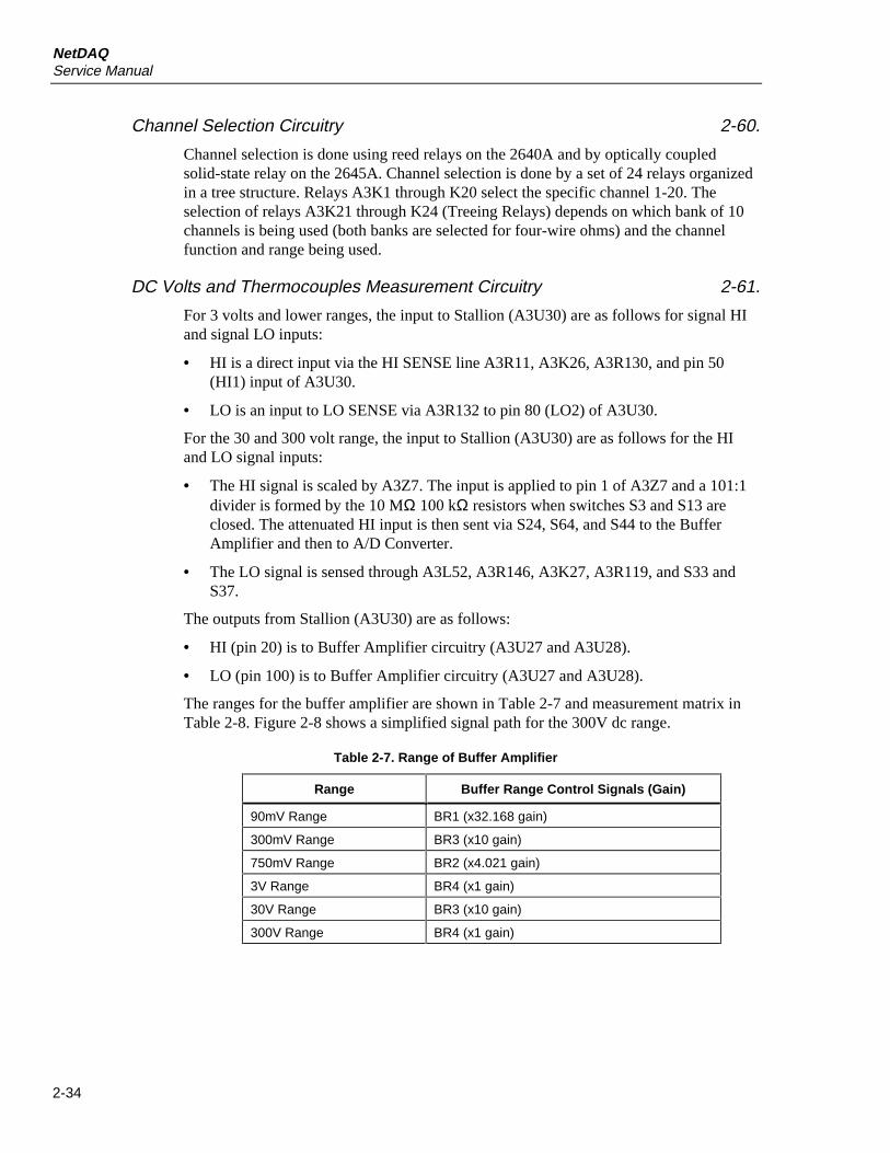
NetDAQService Manual
2-34
Channel Selection Circuitry 2-60.
Channel selection is done using reed relays on the 2640A and by optically coupledsolid-state relay on the 2645A. Channel selection is done by a set of 24 relays organizedin a tree structure. Relays A3K1 through K20 select the specific channel 1-20. Theselection of relays A3K21 through K24 (Treeing Relays) depends on which bank of 10channels is being used (both banks are selected for four-wire ohms) and the channelfunction and range being used.
DC Volts and Thermocouples Measurement Circuitry 2-61.
For 3 volts and lower ranges, the input to Stallion (A3U30) are as follows for signal HIand signal LO inputs:
• HI is a direct input via the HI SENSE line A3R11, A3K26, A3R130, and pin 50(HI1) input of A3U30.
• LO is an input to LO SENSE via A3R132 to pin 80 (LO2) of A3U30.
For the 30 and 300 volt range, the input to Stallion (A3U30) are as follows for the HIand LO signal inputs:
• The HI signal is scaled by A3Z7. The input is applied to pin 1 of A3Z7 and a 101:1divider is formed by the 10 MΩ 100 kΩ resistors when switches S3 and S13 areclosed. The attenuated HI input is then sent via S24, S64, and S44 to the BufferAmplifier and then to A/D Converter.
• The LO signal is sensed through A3L52, A3R146, A3K27, A3R119, and S33 andS37.
The outputs from Stallion (A3U30) are as follows:
• HI (pin 20) is to Buffer Amplifier circuitry (A3U27 and A3U28).
• LO (pin 100) is to Buffer Amplifier circuitry (A3U27 and A3U28).
The ranges for the buffer amplifier are shown in Table 2-7 and measurement matrix inTable 2-8. Figure 2-8 shows a simplified signal path for the 300V dc range.
Table 2-7. Range of Buffer Amplifier
Range Buffer Range Control Signals (Gain)
90mV Range BR1 (x32.168 gain)
300mV Range BR3 (x10 gain)
750mV Range BR2 (x4.021 gain)
3V Range BR4 (x1 gain)
30V Range BR3 (x10 gain)
300V Range BR4 (x1 gain)
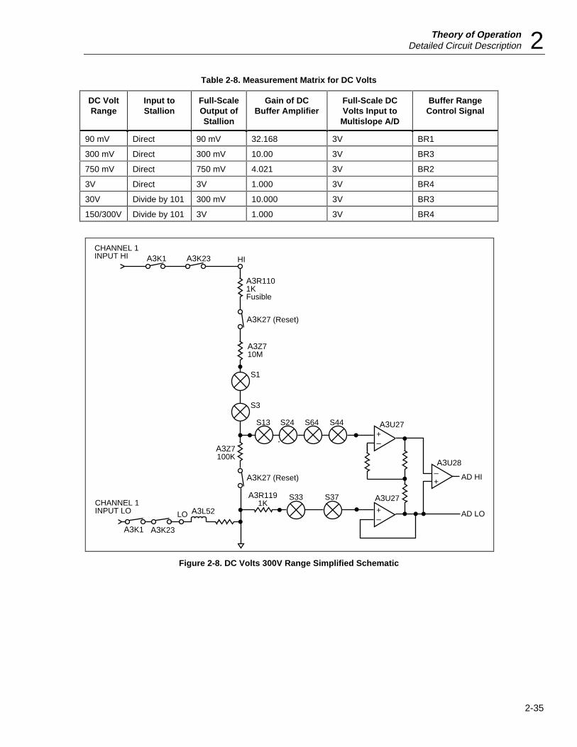
Theory of OperationDetailed Circuit Description 2
2-35
Table 2-8. Measurement Matrix for DC Volts
DC VoltRange
Input toStallion
Full-ScaleOutput ofStallion
Gain of DCBuffer Amplifier
Full-Scale DCVolts Input to
Multislope A/D
Buffer RangeControl Signal
90 mV Direct 90 mV 32.168 3V BR1
300 mV Direct 300 mV 10.00 3V BR3
750 mV Direct 750 mV 4.021 3V BR2
3V Direct 3V 1.000 3V BR4
30V Divide by 101 300 mV 10.000 3V BR3
150/300V Divide by 101 3V 1.000 3V BR4
+_
+_
+
_
CHANNEL 1INPUT HI
CHANNEL 1INPUT LO
A3K1 A3K23 HI
A3R1101KFusible
A3Z710M
S1
S3
S13 S24 S64 S44 A3U27
A3U28
A3U27
AD HI
AD LO
S37S33A3R1191K
A3K27 (Reset)
A3Z7100K
A3K1 A3K23
LO A3L52
A3K27 (Reset)
Figure 2-8. DC Volts 300V Range Simplified Schematic
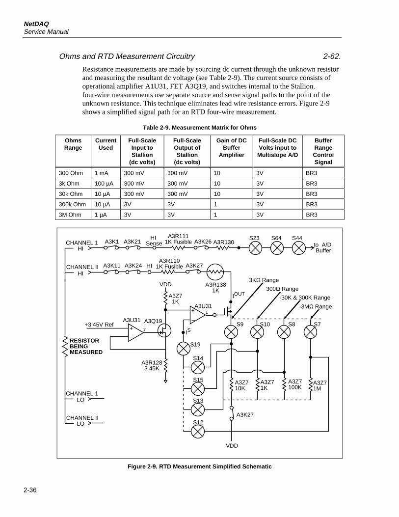
NetDAQService Manual
2-36
Ohms and RTD Measurement Circuitry 2-62.
Resistance measurements are made by sourcing dc current through the unknown resistorand measuring the resultant dc voltage (see Table 2-9). The current source consists ofoperational amplifier A1U31, FET A3Q19, and switches internal to the Stallion.four-wire measurements use separate source and sense signal paths to the point of theunknown resistance. This technique eliminates lead wire resistance errors. Figure 2-9shows a simplified signal path for an RTD four-wire measurement.
Table 2-9. Measurement Matrix for Ohms
OhmsRange
CurrentUsed
Full-ScaleInput toStallion
(dc volts)
Full-ScaleOutput ofStallion
(dc volts)
Gain of DCBuffer
Amplifier
Full-Scale DCVolts input to
Multislope A/D
BufferRangeControlSignal
300 Ohm 1 mA 300 mV 300 mV 10 3V BR3
3k Ohm 100 µA 300 mV 300 mV 10 3V BR3
30k Ohm 10 µA 300 mV 300 mV 10 3V BR3
300k Ohm 10 µA 3V 3V 1 3V BR3
3M Ohm 1 µA 3V 3V 1 3V BR3
CHANNEL 1
CHANNEL II
A3K1 A3K21HI
SenseA3R111
1K Fusible A3K26 A3R130HI
S23 S64 S44to A/D Buffer
A3K11 A3K27HIA3R110
1K FusibleA3K24
A3R1381K
VDD
A3Z71K
A3Q19A3U31+3.45V Ref
+_
7
A3R1283.45K
A3U31+_
1
S19
S14
S15
S13
S12A3K27
VDD
A3Z710K
A3Z71K
A3Z7100K
A3Z71M
S9 S10 S8 S7
IOUT
HI
CHANNEL 1
CHANNEL IILO
LO
3KΩ Range
300Ω Range
-30K & 300K Range
-3MΩ Range
RESISTORBEINGMEASURED
IS
Figure 2-9. RTD Measurement Simplified Schematic
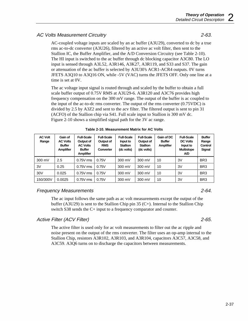
Theory of OperationDetailed Circuit Description 2
2-37
AC Volts Measurement Circuitry 2-63.
AC-coupled voltage inputs are scaled by an ac buffer (A3U29), converted to dc by a truerms ac-to-dc converter (A3U26), filtered by an active ac volt filter, then sent to theStallion IC, the Buffer Amplifier, and the A/D Conversion Circuitry (see Table 2-10).The HI input is switched to the ac buffer through dc blocking capacitor A3C80. The LOinput is sensed through A3L52, A3R146, A3K27, A3R119, and S33 and S37. The gainor attenuation of the ac buffer is selected by A3U30’s ACR1-ACR4 outputs. 0V turnsJFETS A3Q10 to A3Q16 ON, while -5V (VAC) turns the JFETS OFF. Only one line at atime is set at 0V.
The ac voltage input signal is routed through and scaled by the buffer to obtain a fullscale buffer output of 0.75V RMS at A3U29-6. A3R120 and A3C76 provides highfrequency compensation on the 300 mV range. The output of the buffer is ac coupled tothe input of the ac-to-dc rms converter. The output of the rms converter (0.75VDC) isdivided by 2.5 by A3Z2 and sent to the acv filter. The filtered output is sent to pin 31(ACFO) of the Stallion chip via S41. Full scale input to Stallion is 300 mV dc.Figure 2-10 shows a simplified signal path for the 3V ac range.
Table 2-10. Measurement Matrix for AC Volts
AC VoltRange
Gain ofAC Volts
BufferAmplifier
Full-ScaleOutput ofAC Volts
BufferAmplifier
Full-ScaleOutput of
RMSConverter
Full-ScaleInput toStallion
(dc volts)
Full-ScaleOutput ofStallion
(dc volts)
Gain of DCBuffer
Amplifier
Full-ScaleDC VoltsInput to
MultislopeA/D
BufferRangeControlSignal
300 mV 2.5 0.75V rms 0.75V 300 mV 300 mV 10 3V BR3
3V 0.25 0.75V rms 0.75V 300 mV 300 mV 10 3V BR3
30V 0.025 0.75V rms 0.75V 300 mV 300 mV 10 3V BR3
150/300V 0.0025 0.75V rms 0.75V 300 mV 300 mV 10 3V BR3
Frequency Measurements 2-64.
The ac input follows the same path as ac volt measurements except the output of thebuffer (A3U29) is sent to the Stallion Chip pin 35 (C+). Internal to the Stallion Chipswitch S38 sends the C+ input to a frequency comparator and counter.
Active Filter (ACV Filter) 2-65.
The active filter is used only for ac volt measurements to filter out the ac ripple andnoise present on the output of the rms converter. The filter uses an op-amp internal to theStallion Chip, resistors A3R102, A3R103, and A3R104, capacitors A3C57, A3C58, andA3C59. A3Q6 turns on to discharge the capacitors between measurements.
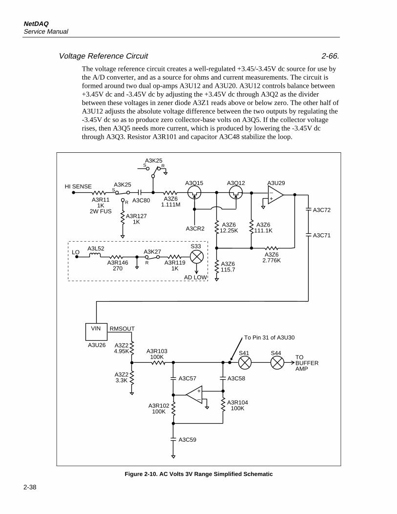
NetDAQService Manual
2-38
Voltage Reference Circuit 2-66.
The voltage reference circuit creates a well-regulated +3.45/-3.45V dc source for use bythe A/D converter, and as a source for ohms and current measurements. The circuit isformed around two dual op-amps A3U12 and A3U20. A3U12 controls balance between+3.45V dc and -3.45V dc by adjusting the +3.45V dc through A3Q2 as the dividerbetween these voltages in zener diode A3Z1 reads above or below zero. The other half ofA3U12 adjusts the absolute voltage difference between the two outputs by regulating the-3.45V dc so as to produce zero collector-base volts on A3Q5. If the collector voltagerises, then A3Q5 needs more current, which is produced by lowering the -3.45V dcthrough A3Q3. Resistor A3R101 and capacitor A3C48 stabilize the loop.
HI SENSE
A3R111K
2W FUS
A3K25S
R
A3R1271K
A3C80
A3K25S R
A3Z61.111M
A3Q15 A3Q12 A3U29
+
_
A3CR2A3Z6
12.25KA3Z6
111.1K
A3Z6115.7
A3Z62.776K
A3C72
A3C71
LOA3L52
A3R146270
R
A3K27
A3R1191K
S33
AD LOW
VIN RMSOUT
A3Z24.95K A3R103
100K
A3C57A3Z23.3K A3C58
A3R102100K
A3R104100K
A3C59
+_
To Pin 31 of A3U30
S41 S44TOBUFFERAMP
A3U26
Figure 2-10. AC Volts 3V Range Simplified Schematic
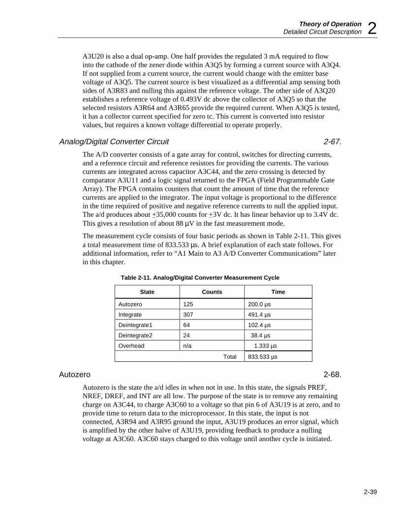
Theory of OperationDetailed Circuit Description 2
2-39
A3U20 is also a dual op-amp. One half provides the regulated 3 mA required to flowinto the cathode of the zener diode within A3Q5 by forming a current source with A3Q4.If not supplied from a current source, the current would change with the emitter basevoltage of A3Q5. The current source is best visualized as a differential amp sensing bothsides of A3R83 and nulling this against the reference voltage. The other side of A3Q20establishes a reference voltage of 0.493V dc above the collector of A3Q5 so that theselected resistors A3R64 and A3R65 provide the required current. When A3Q5 is tested,it has a collector current specified for zero tc. This current is converted into resistorvalues, but requires a known voltage differential to operate properly.
Analog/Digital Converter Circuit 2-67.
The A/D converter consists of a gate array for control, switches for directing currents,and a reference circuit and reference resistors for providing the currents. The variouscurrents are integrated across capacitor A3C44, and the zero crossing is detected bycomparator A3U11 and a logic signal returned to the FPGA (Field Programmable GateArray). The FPGA contains counters that count the amount of time that the referencecurrents are applied to the integrator. The input voltage is proportional to the differencein the time required of positive and negative reference currents to null the applied input.The a/d produces about +35,000 counts for +3V dc. It has linear behavior up to 3.4V dc.This gives a resolution of about 88 µV in the fast measurement mode.
The measurement cycle consists of four basic periods as shown in Table 2-11. This givesa total measurement time of 833.533 µs. A brief explanation of each state follows. Foradditional information, refer to “A1 Main to A3 A/D Converter Communications” laterin this chapter.
Table 2-11. Analog/Digital Converter Measurement Cycle
State Counts Time
Autozero 125 200.0 µs
Integrate 307 491.4 µs
Deintegrate1 64 102.4 µs
Deintegrate2 24 38.4 µs
Overhead n/a 1.333 µs
Total 833.533 µs
Autozero 2-68.
Autozero is the state the a/d idles in when not in use. In this state, the signals PREF,NREF, DREF, and INT are all low. The purpose of the state is to remove any remainingcharge on A3C44, to charge A3C60 to a voltage so that pin 6 of A3U19 is at zero, and toprovide time to return data to the microprocessor. In this state, the input is notconnected, A3R94 and A3R95 ground the input, A3U19 produces an error signal, whichis amplified by the other halve of A3U19, providing feedback to produce a nullingvoltage at A3C60. A3C60 stays charged to this voltage until another cycle is initiated.
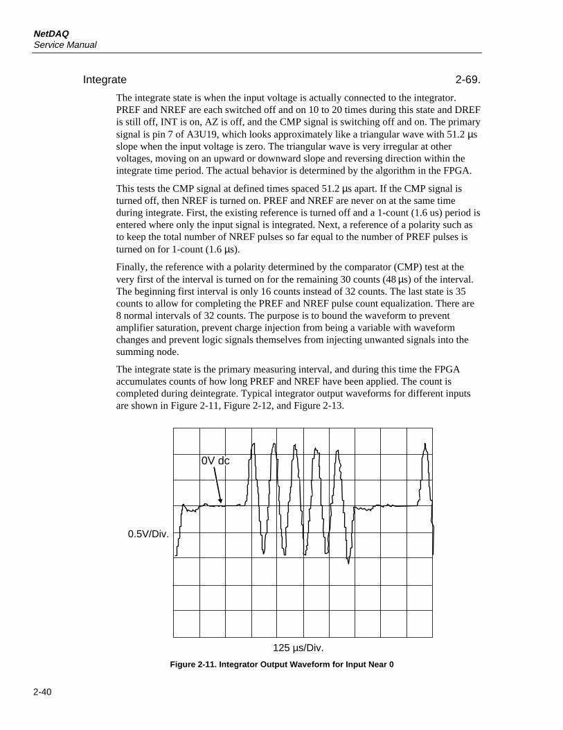
NetDAQService Manual
2-40
Integrate 2-69.
The integrate state is when the input voltage is actually connected to the integrator.PREF and NREF are each switched off and on 10 to 20 times during this state and DREFis still off, INT is on, AZ is off, and the CMP signal is switching off and on. The primarysignal is pin 7 of A3U19, which looks approximately like a triangular wave with 51.2 µsslope when the input voltage is zero. The triangular wave is very irregular at othervoltages, moving on an upward or downward slope and reversing direction within theintegrate time period. The actual behavior is determined by the algorithm in the FPGA.
This tests the CMP signal at defined times spaced 51.2 µs apart. If the CMP signal isturned off, then NREF is turned on. PREF and NREF are never on at the same timeduring integrate. First, the existing reference is turned off and a 1-count (1.6 us) period isentered where only the input signal is integrated. Next, a reference of a polarity such asto keep the total number of NREF pulses so far equal to the number of PREF pulses isturned on for 1-count (1.6 µs).
Finally, the reference with a polarity determined by the comparator (CMP) test at thevery first of the interval is turned on for the remaining 30 counts (48 µs) of the interval.The beginning first interval is only 16 counts instead of 32 counts. The last state is 35counts to allow for completing the PREF and NREF pulse count equalization. There are8 normal intervals of 32 counts. The purpose is to bound the waveform to preventamplifier saturation, prevent charge injection from being a variable with waveformchanges and prevent logic signals themselves from injecting unwanted signals into thesumming node.
The integrate state is the primary measuring interval, and during this time the FPGAaccumulates counts of how long PREF and NREF have been applied. The count iscompleted during deintegrate. Typical integrator output waveforms for different inputsare shown in Figure 2-11, Figure 2-12, and Figure 2-13.
0.5V/Div.
0V dc
125 µs/Div.
Figure 2-11. Integrator Output Waveform for Input Near 0
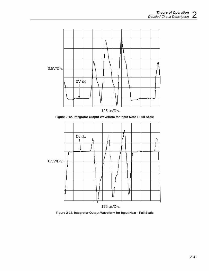
Theory of OperationDetailed Circuit Description 2
2-41
0.5V/Div.
0V dc
125 µs/Div.
Figure 2-12. Integrator Output Waveform for Input Near + Full Scale
0.5V/Div.
0v dc
125 µs/Div.
Figure 2-13. Integrator Output Waveform for Input Near - Full Scale
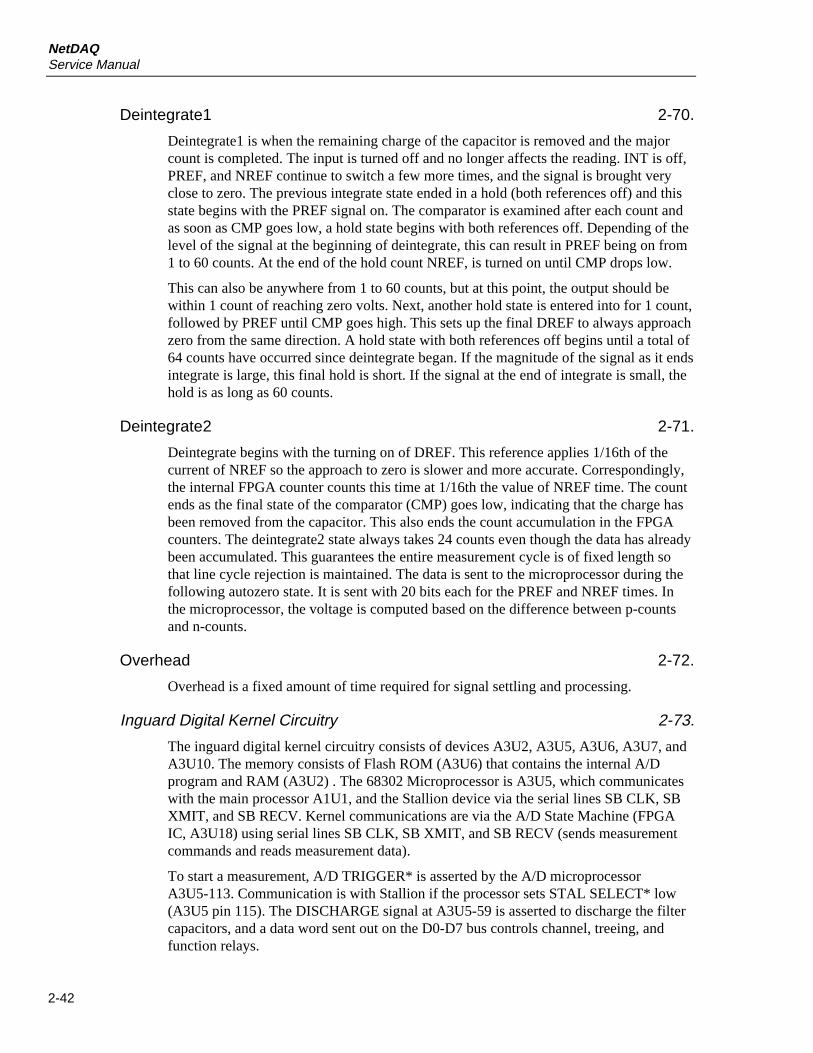
NetDAQService Manual
2-42
Deintegrate1 2-70.
Deintegrate1 is when the remaining charge of the capacitor is removed and the majorcount is completed. The input is turned off and no longer affects the reading. INT is off,PREF, and NREF continue to switch a few more times, and the signal is brought veryclose to zero. The previous integrate state ended in a hold (both references off) and thisstate begins with the PREF signal on. The comparator is examined after each count andas soon as CMP goes low, a hold state begins with both references off. Depending of thelevel of the signal at the beginning of deintegrate, this can result in PREF being on from1 to 60 counts. At the end of the hold count NREF, is turned on until CMP drops low.
This can also be anywhere from 1 to 60 counts, but at this point, the output should bewithin 1 count of reaching zero volts. Next, another hold state is entered into for 1 count,followed by PREF until CMP goes high. This sets up the final DREF to always approachzero from the same direction. A hold state with both references off begins until a total of64 counts have occurred since deintegrate began. If the magnitude of the signal as it endsintegrate is large, this final hold is short. If the signal at the end of integrate is small, thehold is as long as 60 counts.
Deintegrate2 2-71.
Deintegrate begins with the turning on of DREF. This reference applies 1/16th of thecurrent of NREF so the approach to zero is slower and more accurate. Correspondingly,the internal FPGA counter counts this time at 1/16th the value of NREF time. The countends as the final state of the comparator (CMP) goes low, indicating that the charge hasbeen removed from the capacitor. This also ends the count accumulation in the FPGAcounters. The deintegrate2 state always takes 24 counts even though the data has alreadybeen accumulated. This guarantees the entire measurement cycle is of fixed length sothat line cycle rejection is maintained. The data is sent to the microprocessor during thefollowing autozero state. It is sent with 20 bits each for the PREF and NREF times. Inthe microprocessor, the voltage is computed based on the difference between p-countsand n-counts.
Overhead 2-72.
Overhead is a fixed amount of time required for signal settling and processing.
Inguard Digital Kernel Circuitry 2-73.
The inguard digital kernel circuitry consists of devices A3U2, A3U5, A3U6, A3U7, andA3U10. The memory consists of Flash ROM (A3U6) that contains the internal A/Dprogram and RAM (A3U2) . The 68302 Microprocessor is A3U5, which communicateswith the main processor A1U1, and the Stallion device via the serial lines SB CLK, SBXMIT, and SB RECV. Kernel communications are via the A/D State Machine (FPGAIC, A3U18) using serial lines SB CLK, SB XMIT, and SB RECV (sends measurementcommands and reads measurement data).
To start a measurement, A/D TRIGGER* is asserted by the A/D microprocessorA3U5-113. Communication is with Stallion if the processor sets STAL SELECT* low(A3U5 pin 115). The DISCHARGE signal at A3U5-59 is asserted to discharge the filtercapacitors, and a data word sent out on the D0-D7 bus controls channel, treeing, andfunction relays.
Theory of OperationDetailed Circuit Description 2
2-43
Communication with the main processor is done using the IGDR line to receive and theIGDS line to send serial data. On the A/D side, these signals are called RECV DATAand XMIT DATA (pins A3U5-53 and A3U5-54 respectively). The RESET* signal isasserted on power-up for reset and during operation when a break signal is received fromA1U4.
The A/D microprocessor guard crossing is bidirectional. When the user finishes definingthe channels and intervals and starts scanning, the A1 Main PCA downloads all thechannel information to the A3 A/D Converter PCA. The A1 Main PCA uses the guardcrossing to advise the A3 A/D Converter PCA when to start scans, and then return thereadings to the A1 Main PCA. The arrangement keeps the guard-crossing traffic to aminimum when scanning is taking place allowing peak performance during short scanintervals.
Open Thermocouple Detect Circuitry 2-74.
The open thermocouple detect circuitry uses devices A3U23 and A3U32. Before everythermocouple measurement the open T/C check is done by sending a small ac-coupledsignal to the thermocouple input. The A/D Microcomputer (A3U5) initiates the open T/Ctest by asserting OTC_EN and turning ON A3Q20. A 19.2 kHz square wave is sent out theOTCCLK line through A3Q20 and A3C82 to the thermocouple.
The resulting waveform is detected by A3U32 pin 3 and a proportional level is stored onA3C79. If the level is above a threshold level of about 2.7V (Vth) the resistance at the inputis too large (greater than 4 kohm to 10 kohm) and open T/C check is asserted by A3U32pin 7. After a short delay the A/D Microcontroller reads the signal and determines if thethermocouple should be reported to the main processor as open.
A4 Analog Input PCA Circuit Description 2-75.
The Input Connector assembly, which plugs into the A/D Converter PCA from the rearof the instrument, provides 20 pairs of channel terminals for connecting measurementsensors. This assembly also provides the reference junction temperature sensor circuitryused when making thermocouple measurements.
Circuit connections between the Input Connector and A/D Converter PCAs are made viaconnectors A4P1 and A4P2. Input channel and earth ground connections are made viaA4P1, while temperature sensor connections are made through A4P2.
Input connections to channels 1 through 20 are made through terminal blocks TB1 andTB2. Channel 1 and 11 HI and LO terminals incorporate larger creepage and clearancedistances and each have a metal oxide varistor (MOV) to earth ground to clamp voltagetransients. MOVs A4RV1 through A4RV4 limit transient impulses to the morereasonable level of approximately 1800V peak instead of the 2500V peak that can beexpected on 240V ac, IEC 664 Installation Category II, ac mains. In this way, highervoltage ratings can be applied to channels 1 and 11 than can be applied to the other rearchannels.
Strain relief for the user’s sensor wiring is provided both by the Connector PCA housingand the two round pin headers. Each pin of the strain relief headers is electricallyisolated from all other pins and circuitry.
NetDAQService Manual
2-44
Temperature sensor transistor A4Q1 outputs a voltage inversely proportional to thetemperature of the input channel terminals. This voltage is 0.6V dc at 25 °C, increasing2 mV with each degree decrease in temperature, or decreasing 2 mV with each degreeincrease in temperature. For high accuracy, A4Q1 is physically centered within andthermally linked to the 20 input terminals. Local voltage reference A4VR1 and resistorsA4R1 through A4R3 set the calibrated operating current of the temperature sensor.Capacitor A4C1 shunts noise and EMI to ground.
A1 Main to A3 A/D Converter Communications 2-76.The exclusive means of communication between the inguard and outguard is abidirectional, asynchronous, optically-isolated serial link. This link operates at a rate of120,000 baud. The individual bytes are transmitted with eight data bits, one stop bit, andone even parity bit.
The outguard can send either a reset or a command to the inguard. A reset consists of anumber of consecutive break characters, and causes a complete reset of the inguardhardware and software. The inguard returns no response to a reset. A command is asix-byte packet (hereafter referred to as a ’command packet’) that causes the inguard toperform some action and return one or more six-byte response packets. Transactionsbetween the outguard and inguard are always initiated by the outguard. The inguardnever sends data across the guard without being asked to do so.
There are two modes of communication between the inguard and outguard:non-pipelined and pipelined. In the non-pipelined mode, commands and responses aresynchronous, i.e., the outguard waits for the response to a command before sendinganother command. In the pipelined mode, the outguard may send a second commandbefore the first command has completed. The outguard must wait for the response fromthe first command before sending a third command.
Special Codes 2-77.
An ACK response packet is arbitrarily defined as the sequence of bytes (42,0,0,0,0,x)where x is the checksum byte. A NAK response packet is defined as(255,255,255,255,255,x) where x is the checksum byte. A break is an all-zeros characterwithout stop bits.
Resets 2-78.
A reset consists of 5 ms of consecutive break characters sent to the inguard. A hardwarecircuit on the inguard detects this condition and causes a complete reset of the inguardsubsystem. The inguard sends no response to a reset. After sending a reset, the outguardmust wait a predefined amount of time before attempting further communication withthe inguard. This is the same amount of time it waits after a power-up, approximately 3.5seconds.
Theory of OperationA1 Main to A3 A/D Converter Communications 2
2-45
Commands 2-79.
A command consists of a six-byte packet sent from the outguard to the inguard. Themost-significant four bits of the first bytes define the following command types:
• Perform Scan.
• Perform a Self-Test.
• Return A/D Main Firmware Version.
• Return A/D Boot Firmware Version.
• Set Global Configuration.
• Set Channel Configuration.
• Do Houskeeping.
The sixth byte is a checksum. The meanings of the remainder of the bits in the commandpacket vary depending on the command type. The response to all commands is one ormore six-byte response packets. The sixth byte in a packet is always the checksum byte;the meaning of the remainder of the bits depends on the command. The only restrictionis that a response packet should always be distinguishable from a NAK, i.e., it shouldnever have all bits 1.
Perform Scan 2-80.
The Perform Command Packet tells the A/D Converter Assembly to do the following:
• Measure Channel Number if set.
• Return BR1 Zero Offset if set.
• Return BR2 Zero Offset if set.
• Return BR3 Zero Offset if set.
• Return BR4 Zero Offset if set.
• Return Reference Junction Reading if set.
• Return Reference Balance (both references off) reading if set.
• Return Reference Balance (both references on) reading if set.
• Return Checksum.
Action Performed The Perform Scan command causes the inguard to measure eachchannel indicated. These channels must have been previously defined using the SetChannel Configuration command. One response packet is sent to the outguard for eachchannel measured. If any thermocouple channels are requested in this scan, the firstresponse packet is the reference junction reading. If a requested channel has not beendefined, its value is returned as NaN.
There are several bits in the command that exist for debugging purposes only. These bitsindicate that the current stored value for the corresponding housekeeping reading shouldbe returned. The actual value returned for these bits depend on the current measurementrate, since a different value is stored for each measurement rate. Note that these bits donot cause any physical measurement to take place, they simply cause the latest values tobe returned.
NetDAQService Manual
2-46
Response Packets Returned The inguard returns one response packet for the referencejunction reading if any of the measured channels is a thermocouple channel, followed bya response packet for each channel measured, returned in ascending channel order,followed by a response packet for each housekeeping reading specified by the scancommand.
Response Packet Format Each response packet for a Perform Scan command consistsof a floating-point number representing the measurement value, the range used to takethe measurement, the channel number, and the checksum. The floating-point format usedis ANSI/IEEE Std 754-1975 single-precision. Positive and negative overload conditionscause a value of PLUS_OVLD_VAL (0x7f800000) and MINUS_OVLD_VAL(0xff800000), respectively, to be returned. A frequency channel whose input frequencyis too low to measure returns 0 Hz. A channel with an open-thermocouple conditioncauses the value of OTC_VAL (0x7fc00000) to be returned. The inguard waits until ithas completed all measurement activity associated with a particular scan beforebeginning the transmission of the response packets for that scan to the outguard.
The floating-point value returned has a nominal range of -3.0 to +3.0. The outguard mustscale this according to the channel function and range to produce the correct volts orohms. For most ranges, a full-range value is returned as +3.0. For example, on the 300ohm range, +3.0 represents 300 ohms. For the 90 mV and 750 mV ranges, however, +3.0represents 93.26 mV and 0.746083V, respectively. Also, frequency readings alwaysreturn the actual frequency measured and do not require range-scaling by the outguard.
Perform Self-Test 2-81.
The Command Packet tells the A/D to perform all self tests. Response Packets Returnedalways returns a single response packet. The Response Packet Format provides thefollowing:
• A/D self-test result, pass or fail.
• Zero Offset self-test result, pass or fail.
• Reference Balance self-test result, pass or fail.
• Ohms Overload self-test result, pass or fail.
• Open Thermocouple self-test result, pass or fail.
• Checksum
Return Main Firmware Version 2-82.
This Command Packet requests version number of the inguard main firmware andalways returns a single response packet.
Response Packet Format The response consists of five ASCII characters (plus thechecksum byte), in the form txxyy, where t is “F” for FFE (2645A) software and “P” forthe PFE (2640A); xx are the two digits of the major version number, and yy are the twodigits of the minor version number (there is an implicit decimal point between the two).Note that constraining the bytes to be ASCII characters causes the most significant bit ofeach character to be a 0, making the response packet always distinguishable from aNAK.
Theory of OperationA1 Main to A3 A/D Converter Communications 2
2-47
Return Boot Firmware Version 2-83.
This Command Packet Format requests version number of the inguard boot firmwareand always returns a single response packet.
Response Packet Format The response consists of five ASCII characters (plus thechecksum byte), in the form Bxxyy, where B indicates boot software, xx are the twodigits of the major version number, and yy are the two digits of the minor versionnumber (there is an implicit decimal point between the two). Note that constraining thebytes to be ASCII characters causes the most significant bit of each character to be a 0,making the response packet always distinguishable from a NAK.
Set Global Configuration 2-84.
The Command Packet tells the A/D the following:
• Measurement Rate, fast, medium, or slow
• Power Line Frequency, 50 Hz or 60 Hz
• Scheduled Housekeeping Measurements, Enable or Disable
Action Performed Sets global configuration parameters (instrument measurement rate,AC power line frequency, and enable or disable housekeeping measurements). Thedefault state for the inguard is to measure on the fast rate, assuming 60 Hz, and withscheduled housekeeping measurements enabled. The meaning of “scheduledhousekeeping measurements” depends on the current measurement rate.
Response Packets Returned Always returns a single response packet.
Response Packet Format Returns either an ACK packet or a NAK if the commandarguments are not recognized.
Set Channel Configuration 2-85.
The Command Packet tells the A/D the following:
Measurement Function VDC, VAC, 2-Wire Ohms, 4-Wire Ohms, Frequency,Thermocouple, OFF.
Range 90 mV or 300 ohm, 300 mV or 3 kΩ, 3V or 30 kohm, 30V or 300 kΩ, 50V(2645A), 150/300V (2640A), or 3 MΩ, 750 mV (reference junction calibration).
The range field is ignored for frequency and thermocouple channels.
Channel Number 0 to 19 (though user sees channel 1 to 20)
Enable Autorange if bit set (ignored for frequency and thermocouple).
Enable Open Thermocouple Detect if bit set.
Checksum Action Performed is configuration of a single channel to the parametersgiven. The Response Packets Returned always returns a single response packet. TheResponse Packet Format returns an ACK response packet if the channel was successfullyconfigured; otherwise, it returns a NAK.
NetDAQService Manual
2-48
Do Housekeeping 2-86.
The Command Packet tells the A/D to do the following:
• Do all housekeeping readings if bit set.
• Do the next housekeeping reading in the schedule if bit set.
• Prescan: preset the function relays.
Checksum Action Performed is as follows:
• If the Housekeeping bit is 1, the inguard takes a complete set of housekeepingreadings for the current measurement rate (there is one set for each rate).
• If the Next bit is 1, the inguard does the next housekeeping reading indicated by itsinternal schedule. This is the same schedule used for a housekeeping timeout.
• If the Do2 bit is 1, the inguard does the two reference balance readings.
• If the PS bit is 1, the inguard presets the function relays for the first defined channel.
These bits may be set or cleared independently. Note that the actions described above arecarried out regardless of whether scheduled housekeeping is “enabled” by the globalconfiguration command.
Response Packets Returned Always returns a single response packet. This packet isnot returned until the inguard completes all indicated housekeeping measurements.
Response Packet Format Returns a single ACK packet.
Checksums 2-87.
The last byte of each command and response packet is its checksum.
Any time a packet that fails its checksum test is received, it is treated as acommunication error. The inguard transmits a break and waits to be reset. The outguardresets the inguard.
Errors 2-88.
Whenever the inguard encounters an unrecoverable error or a guard-crossingcommunications error (e.g., parity error, overrun), it attempts to send a break characterto the outguard and then goes into a loop, ignoring all subsequent commands from theoutguard, and waits to be reset by the outguard. This insures that all measurementhardware is properly reset. This type of error could be caused by a glitch in the inguardhardware, which is conceivable but rare.
The inguard returns a NAK whenever it receives an illegal command or a command withillegal parameters. Such an error should never occur and probably indicates a softwaredefect. The exception to this is that an error in a scan command returns a break (insteadof a NAK).
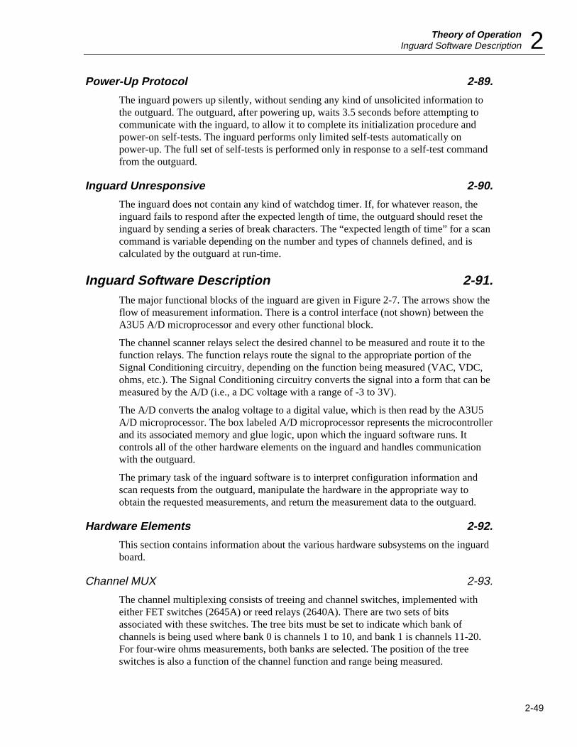
Theory of OperationInguard Software Description 2
2-49
Power-Up Protocol 2-89.
The inguard powers up silently, without sending any kind of unsolicited information tothe outguard. The outguard, after powering up, waits 3.5 seconds before attempting tocommunicate with the inguard, to allow it to complete its initialization procedure andpower-on self-tests. The inguard performs only limited self-tests automatically onpower-up. The full set of self-tests is performed only in response to a self-test commandfrom the outguard.
Inguard Unresponsive 2-90.
The inguard does not contain any kind of watchdog timer. If, for whatever reason, theinguard fails to respond after the expected length of time, the outguard should reset theinguard by sending a series of break characters. The “expected length of time” for a scancommand is variable depending on the number and types of channels defined, and iscalculated by the outguard at run-time.
Inguard Software Description 2-91.The major functional blocks of the inguard are given in Figure 2-7. The arrows show theflow of measurement information. There is a control interface (not shown) between theA3U5 A/D microprocessor and every other functional block.
The channel scanner relays select the desired channel to be measured and route it to thefunction relays. The function relays route the signal to the appropriate portion of theSignal Conditioning circuitry, depending on the function being measured (VAC, VDC,ohms, etc.). The Signal Conditioning circuitry converts the signal into a form that can bemeasured by the A/D (i.e., a DC voltage with a range of -3 to 3V).
The A/D converts the analog voltage to a digital value, which is then read by the A3U5A/D microprocessor. The box labeled A/D microprocessor represents the microcontrollerand its associated memory and glue logic, upon which the inguard software runs. Itcontrols all of the other hardware elements on the inguard and handles communicationwith the outguard.
The primary task of the inguard software is to interpret configuration information andscan requests from the outguard, manipulate the hardware in the appropriate way toobtain the requested measurements, and return the measurement data to the outguard.
Hardware Elements 2-92.
This section contains information about the various hardware subsystems on the inguardboard.
Channel MUX 2-93.
The channel multiplexing consists of treeing and channel switches, implemented witheither FET switches (2645A) or reed relays (2640A). There are two sets of bitsassociated with these switches. The tree bits must be set to indicate which bank ofchannels is being used where bank 0 is channels 1 to 10, and bank 1 is channels 11-20.For four-wire ohms measurements, both banks are selected. The position of the treeswitches is also a function of the channel function and range being measured.
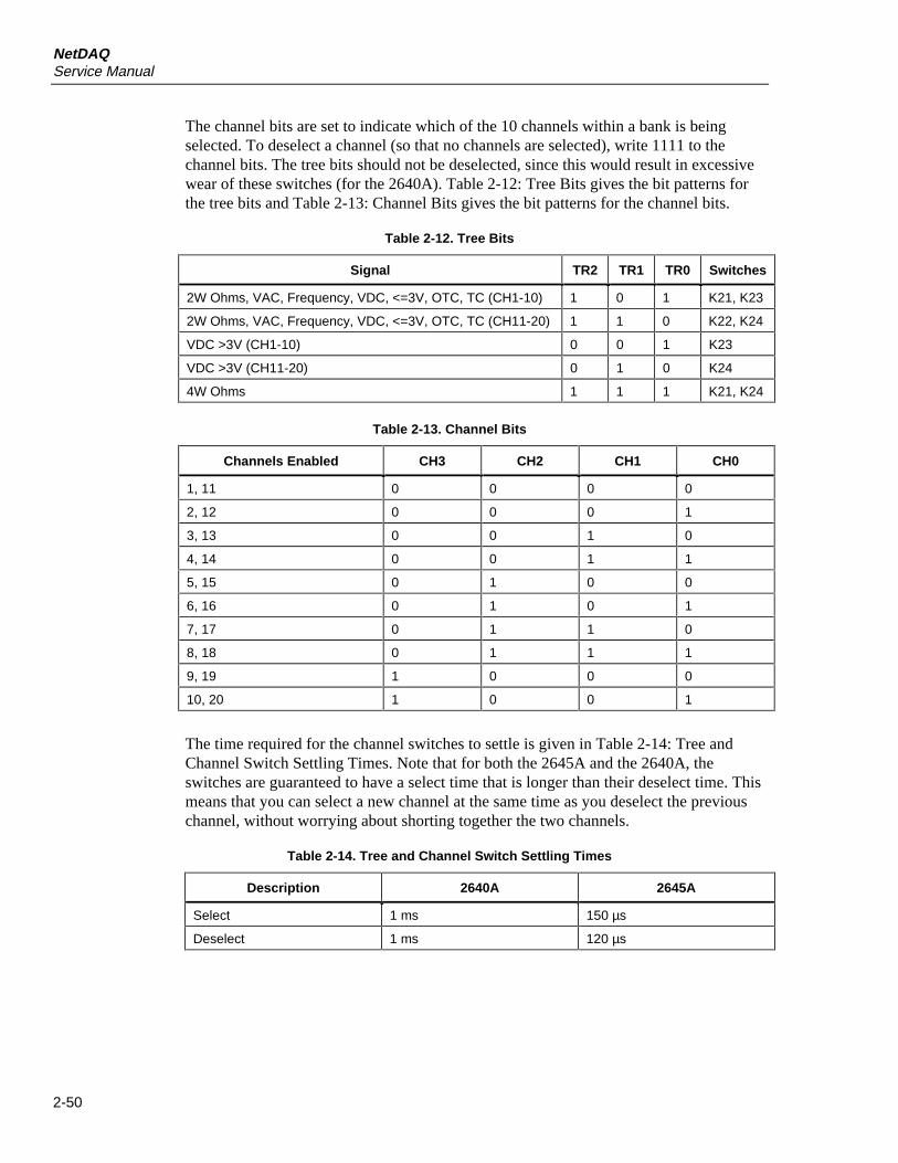
NetDAQService Manual
2-50
The channel bits are set to indicate which of the 10 channels within a bank is beingselected. To deselect a channel (so that no channels are selected), write 1111 to thechannel bits. The tree bits should not be deselected, since this would result in excessivewear of these switches (for the 2640A). Table 2-12: Tree Bits gives the bit patterns forthe tree bits and Table 2-13: Channel Bits gives the bit patterns for the channel bits.
Table 2-12. Tree Bits
Signal TR2 TR1 TR0 Switches
2W Ohms, VAC, Frequency, VDC, <=3V, OTC, TC (CH1-10) 1 0 1 K21, K23
2W Ohms, VAC, Frequency, VDC, <=3V, OTC, TC (CH11-20) 1 1 0 K22, K24
VDC >3V (CH1-10) 0 0 1 K23
VDC >3V (CH11-20) 0 1 0 K24
4W Ohms 1 1 1 K21, K24
Table 2-13. Channel Bits
Channels Enabled CH3 CH2 CH1 CH0
1, 11 0 0 0 0
2, 12 0 0 0 1
3, 13 0 0 1 0
4, 14 0 0 1 1
5, 15 0 1 0 0
6, 16 0 1 0 1
7, 17 0 1 1 0
8, 18 0 1 1 1
9, 19 1 0 0 0
10, 20 1 0 0 1
The time required for the channel switches to settle is given in Table 2-14: Tree andChannel Switch Settling Times. Note that for both the 2645A and the 2640A, theswitches are guaranteed to have a select time that is longer than their deselect time. Thismeans that you can select a new channel at the same time as you deselect the previouschannel, without worrying about shorting together the two channels.
Table 2-14. Tree and Channel Switch Settling Times
Description 2640A 2645A
Select 1 ms 150 µs
Deselect 1 ms 120 µs
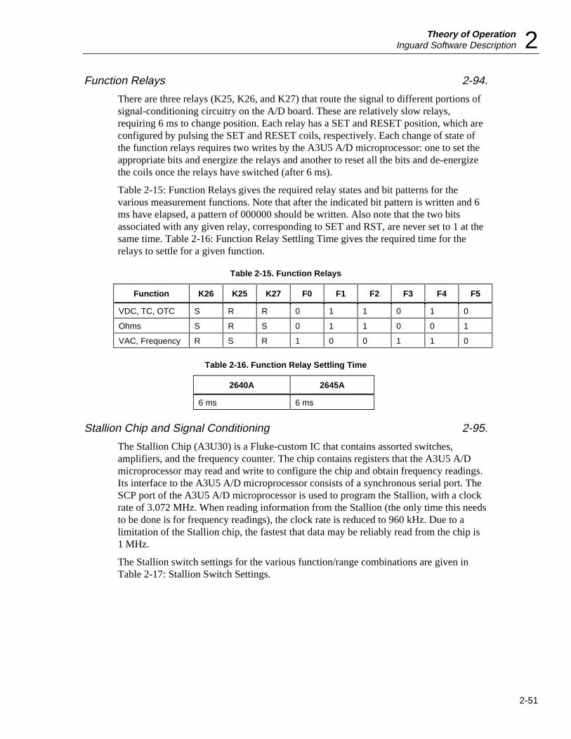
Theory of OperationInguard Software Description 2
2-51
Function Relays 2-94.
There are three relays (K25, K26, and K27) that route the signal to different portions ofsignal-conditioning circuitry on the A/D board. These are relatively slow relays,requiring 6 ms to change position. Each relay has a SET and RESET position, which areconfigured by pulsing the SET and RESET coils, respectively. Each change of state ofthe function relays requires two writes by the A3U5 A/D microprocessor: one to set theappropriate bits and energize the relays and another to reset all the bits and de-energizethe coils once the relays have switched (after 6 ms).
Table 2-15: Function Relays gives the required relay states and bit patterns for thevarious measurement functions. Note that after the indicated bit pattern is written and 6ms have elapsed, a pattern of 000000 should be written. Also note that the two bitsassociated with any given relay, corresponding to SET and RST, are never set to 1 at thesame time. Table 2-16: Function Relay Settling Time gives the required time for therelays to settle for a given function.
Table 2-15. Function Relays
Function K26 K25 K27 F0 F1 F2 F3 F4 F5
VDC, TC, OTC S R R 0 1 1 0 1 0
Ohms S R S 0 1 1 0 0 1
VAC, Frequency R S R 1 0 0 1 1 0
Table 2-16. Function Relay Settling Time
2640A 2645A
6 ms 6 ms
Stallion Chip and Signal Conditioning 2-95.
The Stallion Chip (A3U30) is a Fluke-custom IC that contains assorted switches,amplifiers, and the frequency counter. The chip contains registers that the A3U5 A/Dmicroprocessor may read and write to configure the chip and obtain frequency readings.Its interface to the A3U5 A/D microprocessor consists of a synchronous serial port. TheSCP port of the A3U5 A/D microprocessor is used to program the Stallion, with a clockrate of 3.072 MHz. When reading information from the Stallion (the only time this needsto be done is for frequency readings), the clock rate is reduced to 960 kHz. Due to alimitation of the Stallion chip, the fastest that data may be reliably read from the chip is1 MHz.
The Stallion switch settings for the various function/range combinations are given inTable 2-17: Stallion Switch Settings.
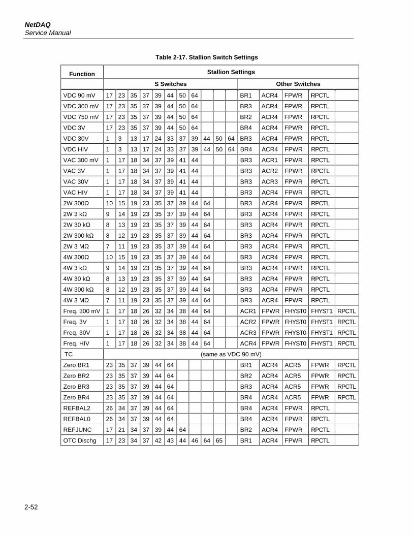
NetDAQService Manual
2-52
Table 2-17. Stallion Switch Settings
Function Stallion Settings
S Switches Other Switches
VDC 90 mV 17 23 35 37 39 44 50 64 BR1 ACR4 FPWR RPCTL
VDC 300 mV 17 23 35 37 39 44 50 64 BR3 ACR4 FPWR RPCTL
VDC 750 mV 17 23 35 37 39 44 50 64 BR2 ACR4 FPWR RPCTL
VDC 3V 17 23 35 37 39 44 50 64 BR4 ACR4 FPWR RPCTL
VDC 30V 1 3 13 17 24 33 37 39 44 50 64 BR3 ACR4 FPWR RPCTL
VDC HIV 1 3 13 17 24 33 37 39 44 50 64 BR4 ACR4 FPWR RPCTL
VAC 300 mV 1 17 18 34 37 39 41 44 BR3 ACR1 FPWR RPCTL
VAC 3V 1 17 18 34 37 39 41 44 BR3 ACR2 FPWR RPCTL
VAC 30V 1 17 18 34 37 39 41 44 BR3 ACR3 FPWR RPCTL
VAC HIV 1 17 18 34 37 39 41 44 BR3 ACR4 FPWR RPCTL
2W 300Ω 10 15 19 23 35 37 39 44 64 BR3 ACR4 FPWR RPCTL
2W 3 kΩ 9 14 19 23 35 37 39 44 64 BR3 ACR4 FPWR RPCTL
2W 30 kΩ 8 13 19 23 35 37 39 44 64 BR3 ACR4 FPWR RPCTL
2W 300 kΩ 8 12 19 23 35 37 39 44 64 BR3 ACR4 FPWR RPCTL
2W 3 MΩ 7 11 19 23 35 37 39 44 64 BR3 ACR4 FPWR RPCTL
4W 300Ω 10 15 19 23 35 37 39 44 64 BR3 ACR4 FPWR RPCTL
4W 3 kΩ 9 14 19 23 35 37 39 44 64 BR3 ACR4 FPWR RPCTL
4W 30 kΩ 8 13 19 23 35 37 39 44 64 BR3 ACR4 FPWR RPCTL
4W 300 kΩ 8 12 19 23 35 37 39 44 64 BR3 ACR4 FPWR RPCTL
4W 3 MΩ 7 11 19 23 35 37 39 44 64 BR3 ACR4 FPWR RPCTL
Freq. 300 mV 1 17 18 26 32 34 38 44 64 ACR1 FPWR FHYST0 FHYST1 RPCTL
Freq. 3V 1 17 18 26 32 34 38 44 64 ACR2 FPWR FHYST0 FHYST1 RPCTL
Freq. 30V 1 17 18 26 32 34 38 44 64 ACR3 FPWR FHYST0 FHYST1 RPCTL
Freq. HIV 1 17 18 26 32 34 38 44 64 ACR4 FPWR FHYST0 FHYST1 RPCTL
TC (same as VDC 90 mV)
Zero BR1 23 35 37 39 44 64 BR1 ACR4 ACR5 FPWR RPCTL
Zero BR2 23 35 37 39 44 64 BR2 ACR4 ACR5 FPWR RPCTL
Zero BR3 23 35 37 39 44 64 BR3 ACR4 ACR5 FPWR RPCTL
Zero BR4 23 35 37 39 44 64 BR4 ACR4 ACR5 FPWR RPCTL
REFBAL2 26 34 37 39 44 64 BR4 ACR4 FPWR RPCTL
REFBAL0 26 34 37 39 44 64 BR4 ACR4 FPWR RPCTL
REFJUNC 17 21 34 37 39 44 64 BR2 ACR4 FPWR RPCTL
OTC Dischg 17 23 34 37 42 43 44 46 64 65 BR1 ACR4 FPWR RPCTL
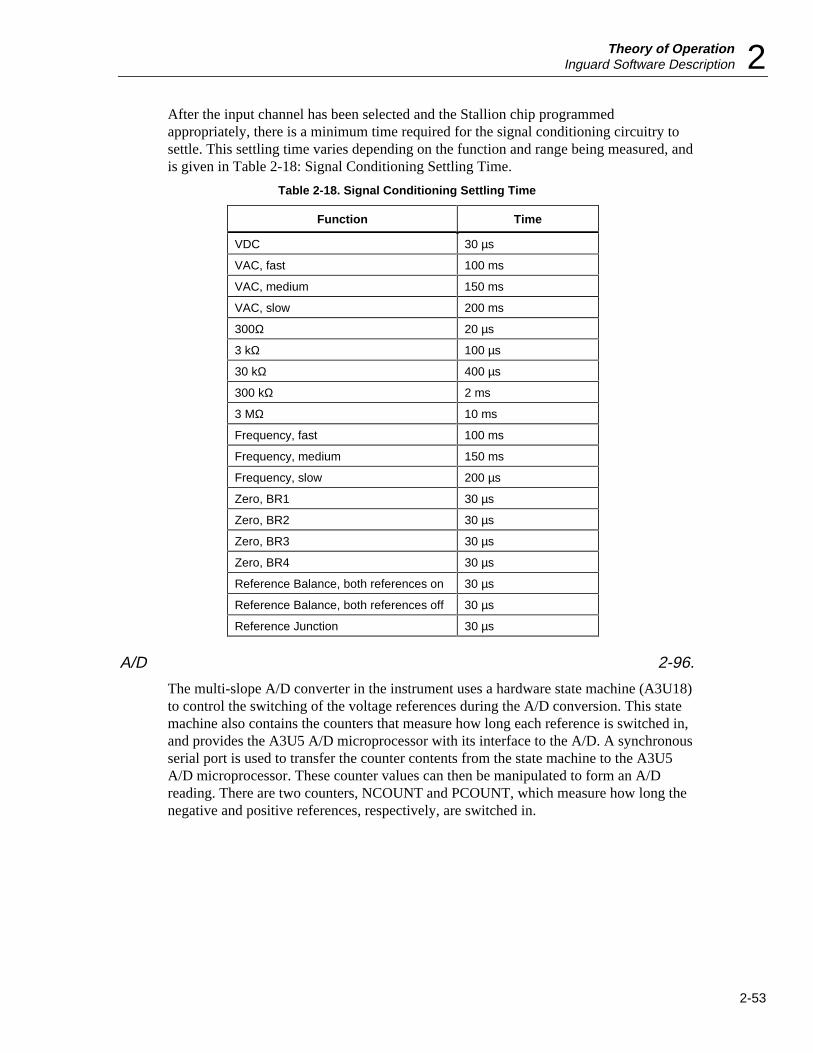
Theory of OperationInguard Software Description 2
2-53
After the input channel has been selected and the Stallion chip programmedappropriately, there is a minimum time required for the signal conditioning circuitry tosettle. This settling time varies depending on the function and range being measured, andis given in Table 2-18: Signal Conditioning Settling Time.
Table 2-18. Signal Conditioning Settling Time
Function Time
VDC 30 µs
VAC, fast 100 ms
VAC, medium 150 ms
VAC, slow 200 ms
300Ω 20 µs
3 kΩ 100 µs
30 kΩ 400 µs
300 kΩ 2 ms
3 MΩ 10 ms
Frequency, fast 100 ms
Frequency, medium 150 ms
Frequency, slow 200 µs
Zero, BR1 30 µs
Zero, BR2 30 µs
Zero, BR3 30 µs
Zero, BR4 30 µs
Reference Balance, both references on 30 µs
Reference Balance, both references off 30 µs
Reference Junction 30 µs
A/D 2-96.
The multi-slope A/D converter in the instrument uses a hardware state machine (A3U18)to control the switching of the voltage references during the A/D conversion. This statemachine also contains the counters that measure how long each reference is switched in,and provides the A3U5 A/D microprocessor with its interface to the A/D. A synchronousserial port is used to transfer the counter contents from the state machine to the A3U5A/D microprocessor. These counter values can then be manipulated to form an A/Dreading. There are two counters, NCOUNT and PCOUNT, which measure how long thenegative and positive references, respectively, are switched in.
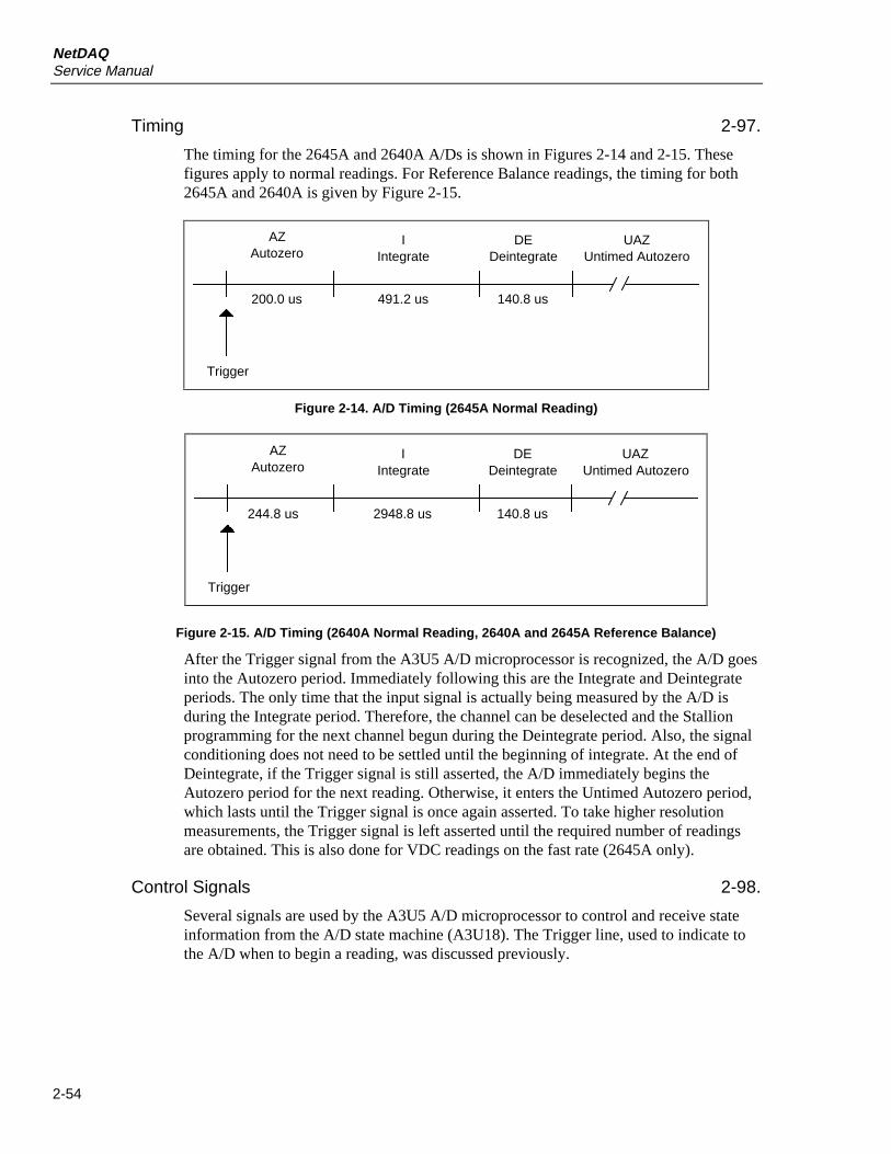
NetDAQService Manual
2-54
Timing 2-97.
The timing for the 2645A and 2640A A/Ds is shown in Figures 2-14 and 2-15. Thesefigures apply to normal readings. For Reference Balance readings, the timing for both2645A and 2640A is given by Figure 2-15.
AZAutozero
IIntegrate
DEDeintegrate
UAZUntimed Autozero
Trigger
200.0 us 491.2 us 140.8 us
Figure 2-14. A/D Timing (2645A Normal Reading)
AZAutozero
IIntegrate
DEDeintegrate
UAZUntimed Autozero
Trigger
140.8 us244.8 us 2948.8 us
Figure 2-15. A/D Timing (2640A Normal Reading, 2640A and 2645A Reference Balance)
After the Trigger signal from the A3U5 A/D microprocessor is recognized, the A/D goesinto the Autozero period. Immediately following this are the Integrate and Deintegrateperiods. The only time that the input signal is actually being measured by the A/D isduring the Integrate period. Therefore, the channel can be deselected and the Stallionprogramming for the next channel begun during the Deintegrate period. Also, the signalconditioning does not need to be settled until the beginning of integrate. At the end ofDeintegrate, if the Trigger signal is still asserted, the A/D immediately begins theAutozero period for the next reading. Otherwise, it enters the Untimed Autozero period,which lasts until the Trigger signal is once again asserted. To take higher resolutionmeasurements, the Trigger signal is left asserted until the required number of readingsare obtained. This is also done for VDC readings on the fast rate (2645A only).
Control Signals 2-98.
Several signals are used by the A3U5 A/D microprocessor to control and receive stateinformation from the A/D state machine (A3U18). The Trigger line, used to indicate tothe A/D when to begin a reading, was discussed previously.
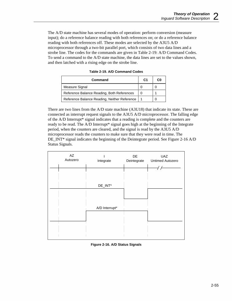
Theory of OperationInguard Software Description 2
2-55
The A/D state machine has several modes of operation: perform conversion (measureinput); do a reference balance reading with both references on; or do a reference balancereading with both references off. These modes are selected by the A3U5 A/Dmicroprocessor through a two-bit parallel port, which consists of two data lines and astrobe line. The codes for the commands are given in Table 2-19: A/D Command Codes.To send a command to the A/D state machine, the data lines are set to the values shown,and then latched with a rising edge on the strobe line.
Table 2-19. A/D Command Codes
Command C1 C0
Measure Signal 0 0
Reference Balance Reading, Both References 0 1
Reference Balance Reading, Neither Reference 1 0
There are two lines from the A/D state machine (A3U18) that indicate its state. These areconnected as interrupt request signals to the A3U5 A/D microprocessor. The falling edgeof the A/D Interrupt* signal indicates that a reading is complete and the counters areready to be read. The A/D Interrupt* signal goes high at the beginning of the Integrateperiod, when the counters are cleared, and the signal is read by the A3U5 A/Dmicroprocessor reads the counters to make sure that they were read in time. TheDE_INT* signal indicates the beginning of the Deintegrate period. See Figure 2-16 A/DStatus Signals.
AZAutozero
IIntegrate
DEDeintegrate
UAZUntimed Autozero
DE_INT*
A/D Interrupt*
Figure 2-16. A/D Status Signals
NetDAQService Manual
2-56
Counters 2-99.
The counters in the A/D state machine (A3U18) are accessed through a synchronousserial interface. This interface is connected to the SCP port of the A3U5 A/Dmicroprocessor, which is also connected to the Stallion chip. Chip-select lines are usedto indicate the device the A3U5 A/D microprocessor is communicating. The countervalues from the A/D are transmitted in five bytes. The hardware state machine transmitsbytes most-significant bit first. There is no hardware detection of overload. An overloadcondition is detected by a software check of the PCOUNT and NCOUNT values. Thehardware is designed so that there are sufficient guard bits on the A/D counters to avoidoverflow.
The counters are cleared at the beginning of the Integrate period. This means that whentaking continuous readings, the A3U5 A/D microprocessor has only the length of theAutozero period to read the counters.
Converting Counts to Volts 2-100.
If we assume perfect voltage references and no offsets, the basic formula for obtainingvolts from N and P counts is as follows:
V = (16P - N)K
where
V = volts
P = P counts
N = N counts
K = (0.1)(2)(3.45) / (16) / (307) / (1.6) (2645A)
K = (0.1)(2)(3.45) / (16) / (1843) / (1.6) (2640A)
For higher resolution measurements, P and N counts are accumulated for the totalnumber of A/D readings in the measurement and then used in the above formula. We callthese Ptot and Ntot. The final voltage is then divided by the number of A/D readings inthe measurement.
In reality, we do not have perfect references, so we must apply a scale factor. The scalefactor is applied to P counts in the above formula, giving:
V = (16PS - N)K
where
S = scale factor
The scale factor is derived from the reference balance readings. See Reference BalanceReadings. The scale factor has a nominal value of 1.0, and a typical value between 0.99and 1.01.
Theory of OperationInguard Software Description 2
2-57
We also must subtract the correct zero offset from the measurement. There are four zerooffsets, one for each DC buffer amplifier gain setting (BR1, BR2, BR3, or BR4). Thegain setting used for a particular function and range can be determined from the Stallionswitch settings (Table 2-17: Stallion Switch Settings). The final formula is therefore
V = (16PtotS - Ntot)K - Z
where
Ptot = P counts (total)
Ntot = N counts (total)
Z = zero offset.
Zero offsets are also covered in “Zero Offset Readings” later in this chapter.
DISCHARGE Signal 2-101.
The signal DISCHARGE is driven by the A3U5 A/D microprocessor (pin 59) throughone of its parallel port pins and controls the discharge of certain filter capacitors. Thisline is normally left low. It is driven high during the VAC discharge mode. See “VACDischarge Mode” later in this chapter for more information.
Open-Thermocouple Detector 2-102.
To check for an open thermocouple input, the appropriate channel is selected with thefunction relays also set to the appropriate position, and the OTC circuitry is enabled.This is done by setting the OTC_EN bit high and turning on the OTC_CLK signal, witha frequency of 19.2 kHz. OTC_CLK is supplied by the A3U5 A/D microprocessor in theform of the SCC3 baud rate generator (BRG3 pin). After 1.7 ms, the OTC bit is read todetermine the status of the channel. A 1 represents an open thermocouple.
After the reading, the OTC_CLK signal is turned off by setting it high. Then theOTC_EN bit is set low.
After deselecting the channel, the measurement circuitry that has been charged by theOTC test must be discharged. This is done by programming Stallion to apply a shortbetween its HI1 pin and ground, setting OTC_CLK low, and setting OTC_EN high. Thisshort is maintained for 500 us. After this, OTC_CLK is set high again, and OTC_EN isset low.
Channel Measurements 2-103.
The following paragraphs describe the Channel Measurement characteristics.
Reading Rates 2-104.
The instrument has three reading rates: fast, medium, and slow. These measurementrates allow you to obtain higher resolution and accuracy at the expense of slowermeasurements. The instrument obtains higher resolution measurements by averagingmultiple A/D readings and/or waiting longer for signal conditioning to settle. Thenumber of A/D readings averaged together to obtain a single measurement is givenbelow in Table 2-20: A/D Readings to Average to Obtain a Measurement. Multiple A/Dreadings taken to average to obtain a measurement must be taken back-to-back, withoutinterruption, in order to obtain AC line-frequency rejection.
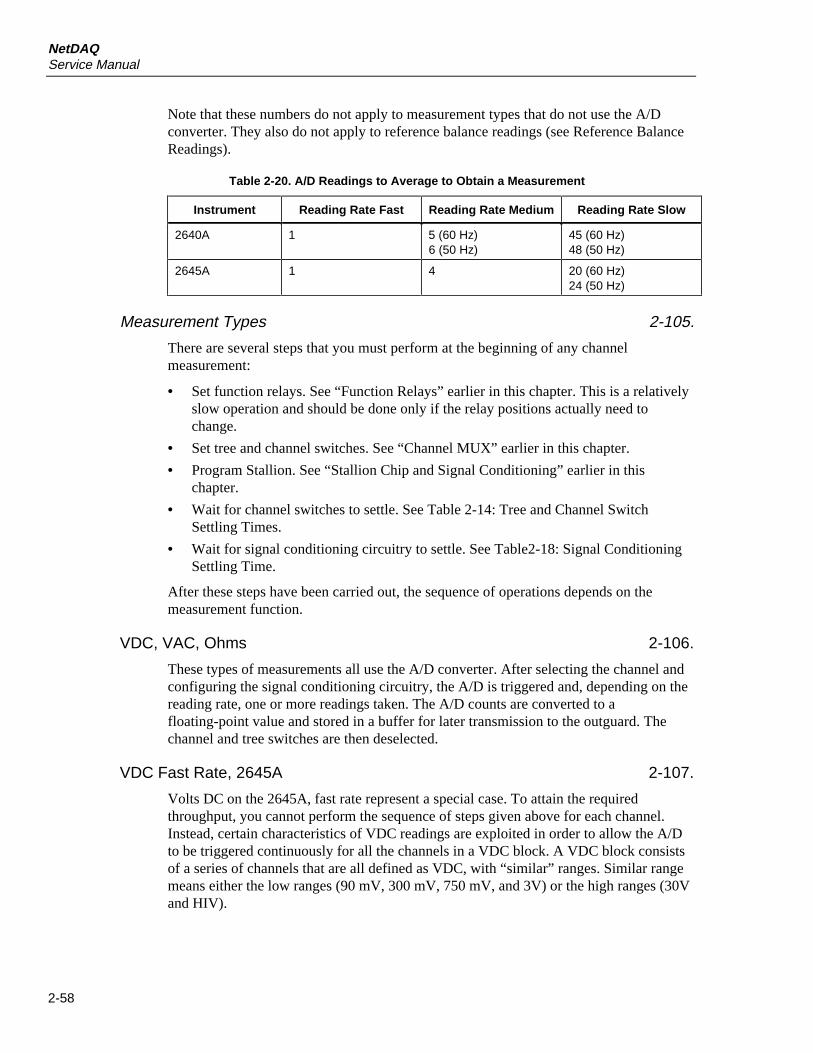
NetDAQService Manual
2-58
Note that these numbers do not apply to measurement types that do not use the A/Dconverter. They also do not apply to reference balance readings (see Reference BalanceReadings).
Table 2-20. A/D Readings to Average to Obtain a Measurement
Instrument Reading Rate Fast Reading Rate Medium Reading Rate Slow
2640A 1 5 (60 Hz)6 (50 Hz)
45 (60 Hz)48 (50 Hz)
2645A 1 4 20 (60 Hz)24 (50 Hz)
Measurement Types 2-105.
There are several steps that you must perform at the beginning of any channelmeasurement:
• Set function relays. See “Function Relays” earlier in this chapter. This is a relativelyslow operation and should be done only if the relay positions actually need tochange.
• Set tree and channel switches. See “Channel MUX” earlier in this chapter.
• Program Stallion. See “Stallion Chip and Signal Conditioning” earlier in thischapter.
• Wait for channel switches to settle. See Table 2-14: Tree and Channel SwitchSettling Times.
• Wait for signal conditioning circuitry to settle. See Table2-18: Signal ConditioningSettling Time.
After these steps have been carried out, the sequence of operations depends on themeasurement function.
VDC, VAC, Ohms 2-106.
These types of measurements all use the A/D converter. After selecting the channel andconfiguring the signal conditioning circuitry, the A/D is triggered and, depending on thereading rate, one or more readings taken. The A/D counts are converted to afloating-point value and stored in a buffer for later transmission to the outguard. Thechannel and tree switches are then deselected.
VDC Fast Rate, 2645A 2-107.
Volts DC on the 2645A, fast rate represent a special case. To attain the requiredthroughput, you cannot perform the sequence of steps given above for each channel.Instead, certain characteristics of VDC readings are exploited in order to allow the A/Dto be triggered continuously for all the channels in a VDC block. A VDC block consistsof a series of channels that are all defined as VDC, with “similar” ranges. Similar rangemeans either the low ranges (90 mV, 300 mV, 750 mV, and 3V) or the high ranges (30Vand HIV).
Theory of OperationInguard Software Description 2
2-59
For the channels within such a block, we can assume the following:
• No function relay switches are required.
• There is only one Stallion register, that must be written to between channels.
• A channel can be selected at the beginning of the deintegrate period of the previouschannel, at the same time that the previous channel is deselected.
• There is sufficient time during the deintegrate period to configure the Stallion for thenext channel.
• There is sufficient time during the autozero period of a channel for signalconditioning settling.
• The N and P counters for a channel can be read during the autozero period of thenext channel.
Thermocouples 2-108.
A thermocouple channel is measured in the same way as a volts DC channel, on the90 mV range. However, before deselecting the channel at the end of the measurement, anopen-thermocouple check may be done, if the channel is so configured. An “open”indication from this check causes a value of OTC_VAL to be returned for the channelmeasurement, regardless of the voltage measured. See Open-Thermocouple Detector.
Thermocouple readings also require an isothermal block reference junction reading to betaken. If any thermocouple channels are measured in a scan, a reference junctionmeasurement is taken first, before any channel measurements.
Reference Junction 2-109.
The reference junction reading is similar to a VDC reading. However, no channelselection or function relay switching is required; however, the Stallion must beconfigured. The reference junction reading is converted to a floating-point value andreturned to the outguard.
Frequency 2-110.
There are actually two parts to a frequency measurement. First, a normal VACmeasurement is taken using the highest range. You must do this to determine theamplitude of the input signal, and thus the most appropriate gain setting to use for theactual frequency measurement. The frequency measurement circuitry works best with alarge amplitude input signal.
Therefore, the gain setting used is one higher than would be used for a normal VACmeasurement. For example, if the autosensitivity reading indicates that the inputamplitude is 3V, you take the frequency measurement is taken with the AC bufferamplifier set to the 300 mV range. See Table 2-21: Frequency Sensitivity. For inputsignals whose measured amplitude is very low, a frequency reading is still attempted,since the frequency response of the VAC measurement circuitry rolls off more quickly athigher frequencies than that of the frequency measurement circuitry.
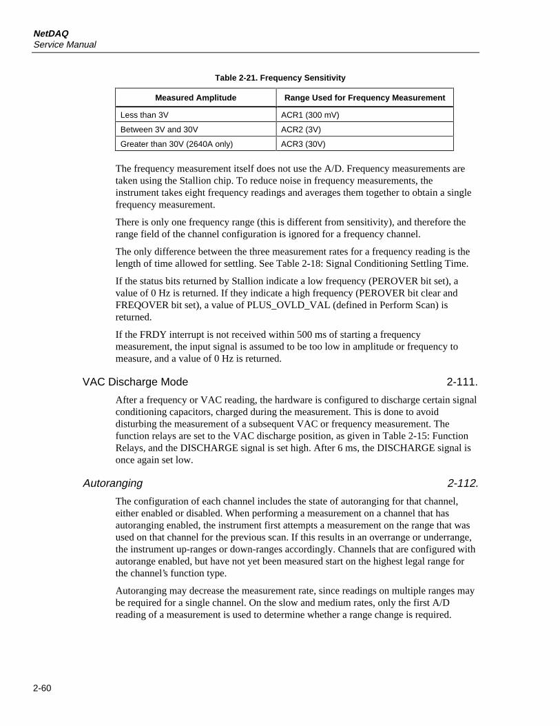
NetDAQService Manual
2-60
Table 2-21. Frequency Sensitivity
Measured Amplitude Range Used for Frequency Measurement
Less than 3V ACR1 (300 mV)
Between 3V and 30V ACR2 (3V)
Greater than 30V (2640A only) ACR3 (30V)
The frequency measurement itself does not use the A/D. Frequency measurements aretaken using the Stallion chip. To reduce noise in frequency measurements, theinstrument takes eight frequency readings and averages them together to obtain a singlefrequency measurement.
There is only one frequency range (this is different from sensitivity), and therefore therange field of the channel configuration is ignored for a frequency channel.
The only difference between the three measurement rates for a frequency reading is thelength of time allowed for settling. See Table 2-18: Signal Conditioning Settling Time.
If the status bits returned by Stallion indicate a low frequency (PEROVER bit set), avalue of 0 Hz is returned. If they indicate a high frequency (PEROVER bit clear andFREQOVER bit set), a value of PLUS_OVLD_VAL (defined in Perform Scan) isreturned.
If the FRDY interrupt is not received within 500 ms of starting a frequencymeasurement, the input signal is assumed to be too low in amplitude or frequency tomeasure, and a value of 0 Hz is returned.
VAC Discharge Mode 2-111.
After a frequency or VAC reading, the hardware is configured to discharge certain signalconditioning capacitors, charged during the measurement. This is done to avoiddisturbing the measurement of a subsequent VAC or frequency measurement. Thefunction relays are set to the VAC discharge position, as given in Table 2-15: FunctionRelays, and the DISCHARGE signal is set high. After 6 ms, the DISCHARGE signal isonce again set low.
Autoranging 2-112.
The configuration of each channel includes the state of autoranging for that channel,either enabled or disabled. When performing a measurement on a channel that hasautoranging enabled, the instrument first attempts a measurement on the range that wasused on that channel for the previous scan. If this results in an overrange or underrange,the instrument up-ranges or down-ranges accordingly. Channels that are configured withautorange enabled, but have not yet been measured start on the highest legal range forthe channel’s function type.
Autoranging may decrease the measurement rate, since readings on multiple ranges maybe required for a single channel. On the slow and medium rates, only the first A/Dreading of a measurement is used to determine whether a range change is required.
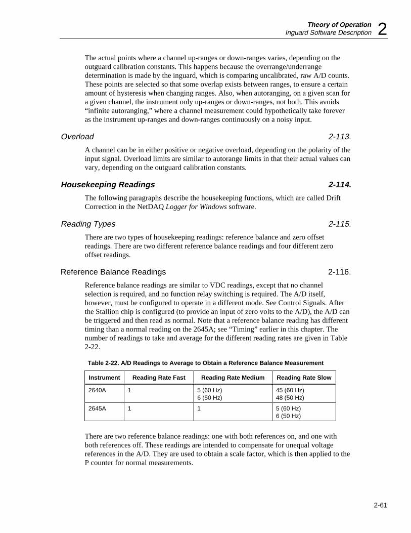
Theory of OperationInguard Software Description 2
2-61
The actual points where a channel up-ranges or down-ranges varies, depending on theoutguard calibration constants. This happens because the overrange/underrangedetermination is made by the inguard, which is comparing uncalibrated, raw A/D counts.These points are selected so that some overlap exists between ranges, to ensure a certainamount of hysteresis when changing ranges. Also, when autoranging, on a given scan fora given channel, the instrument only up-ranges or down-ranges, not both. This avoids“infinite autoranging,” where a channel measurement could hypothetically take foreveras the instrument up-ranges and down-ranges continuously on a noisy input.
Overload 2-113.
A channel can be in either positive or negative overload, depending on the polarity of theinput signal. Overload limits are similar to autorange limits in that their actual values canvary, depending on the outguard calibration constants.
Housekeeping Readings 2-114.
The following paragraphs describe the housekeeping functions, which are called DriftCorrection in the NetDAQ Logger for Windows software.
Reading Types 2-115.
There are two types of housekeeping readings: reference balance and zero offsetreadings. There are two different reference balance readings and four different zerooffset readings.
Reference Balance Readings 2-116.
Reference balance readings are similar to VDC readings, except that no channelselection is required, and no function relay switching is required. The A/D itself,however, must be configured to operate in a different mode. See Control Signals. Afterthe Stallion chip is configured (to provide an input of zero volts to the A/D), the A/D canbe triggered and then read as normal. Note that a reference balance reading has differenttiming than a normal reading on the 2645A; see “Timing” earlier in this chapter. Thenumber of readings to take and average for the different reading rates are given in Table2-22.
Table 2-22. A/D Readings to Average to Obtain a Reference Balance Measurement
Instrument Reading Rate Fast Reading Rate Medium Reading Rate Slow
2640A 1 5 (60 Hz)6 (50 Hz)
45 (60 Hz)48 (50 Hz)
2645A 1 1 5 (60 Hz)6 (50 Hz)
There are two reference balance readings: one with both references on, and one withboth references off. These readings are intended to compensate for unequal voltagereferences in the A/D. They are used to obtain a scale factor, which is then applied to theP counter for normal measurements.
NetDAQService Manual
2-62
The scale factor is derived as follows:
S = 1 - [(16P2 - N2) - (16P0 - N0)]K2
where
S = scale factor
P2 = P counts (both references on)
N2 = N counts (both references on)
P0 = P counts (both references off)
N0 = N counts (both references off)
K2 = (0.1) / (16) / (1843) / (1.6)
Zero Offset Readings 2-117.
There are four zero readings: one for each gain setting of the DC buffer amplifier. Zerooffset readings are similar to VDC readings, except that no channel selection is requiredand no function relay switching is required. The Stallion chip must be configured. TheA/D is placed in normal measurement mode. The number of readings to average is thesame as for a normal reading (see Table 2-20: A/D Readings to Average to Obtain aMeasurement). Zero offset measurements are converted to volts in the same way asnormal channel measurements, except, of course, that no zero offset is subtracted. Thereference balance scale factor is used.
Housekeeping Schedule 2-118.
Housekeeping readings are always taken in response to a “Do Housekeeping” commandfrom the outguard, as described in “Do Housekeeping” earlier in this chapter.
Setting the HK bit in a configuration command causes the inguard to schedulehousekeeping readings on a rotating basis, taking one at the end of each channel scan. Italso enables a timer, which is started at the end of a scan or after a configurationcommand. Whenever the timer expires, the next housekeeping reading in the schedule ismeasured, and the timer is restarted. The timer is set to expire after 17.476 seconds.
On the medium and slow rate, all six housekeeping readings are scheduled as describedin the preceding paragraph. On the fast rate, however, only zero offset readings arescheduled. This is because a single reference balance reading is longer than a normalreading on the fast rate, which would cause scans containing them to take longer.
Self-Tests 2-119.
There are two series of self-tests performed by the inguard: those done automatically atpower-up, and those done in response to a self-test command from the outguard.
Power-Up Self-Tests 2-120.
On power-up the inguard performs a ROM checksum test and a destructive RAM test. Ifeither of these tests fail, the inguard treats it as a fatal error and enters the boot monitor.No explicit indication of either of these tests failing is given to the outguard.
Theory of OperationInguard Software Description 2
2-63
Self-Test Command 2-121.
The self-test command from the outguard causes the following tests to be performed, inthe order given. If the A/D test fails, the tests that require the A/D (zero offset test,reference balance test, ohms overload test) are not done.
A/D Test 2-122.
This test simply triggers the A/D and waits for either the A/D interrupt or a timeout. Ifthe timeout occurs before receiving an A/D interrupt, the test fails and the A/D isassumed to be non-functional. The timeout is set to 10 ms, greater than either the 2640Aor 2645A A/D reading time.
Zero Offset Test 2-123.
The zero offset test measures the four zero offsets, and ascertains that they are withinreasonable limits. The test fails if any of the offsets measures greater than 2000 counts(2645A) or 12000 counts (2640A). This is approximately 0.175 volts. A typical zerooffset measurement is approximately 0.1 volts.
Reference Balance Test 2-124.
The reference balance test measures the two reference balance values. The individualcounter values (N counts and P counts) are tested against limits, as are the differencesbetween the counter values. For both references on, each counter must be less than0x8000, and their difference must be less than 0x6000. For both references off, eachcounter must be less than 0x2000, and their difference must be less than 0x200.
Ohms Overload Test 2-125.
For this test, a two-wire ohms measurement is attempted without any channel selected(however the tree and function relays must be set). This should result in an overload.Any other value causes the test to fail.
OTC Test 2-126.
The OTC test attempts to do an open-thermocouple check with no channel selected.Unless this results in an “open” indication, the test fails.

NetDAQService Manual
2-64
3-1
Chapter 3General Maintenance
Title Page
3-1. Introduction ............................................................................................ 3-33-2. Warranty Repairs and Shipping ............................................................. 3-33-3. General Maintenance.............................................................................. 3-33-4. Required Equipment .......................................................................... 3-33-5. Power Requirements .......................................................................... 3-33-6. Static-Safe Handling .......................................................................... 3-33-7. Servicing Surface-Mount Assemblies ............................................... 3-43-8. Cleaning.................................................................................................. 3-43-9. Replacing the Line Fuse......................................................................... 3-53-10. Disassembly Procedures......................................................................... 3-73-11. Removing the Instrument Case.......................................................... 3-73-12. Removing the Front Panel Assembly ................................................ 3-73-13. Disassembling the Front Panel Assembly ......................................... 3-113-14. Removing the A1 Main PCA............................................................. 3-113-15. Removing the A2 Display PCA......................................................... 3-123-16. Removing the A3 A/D Converter PCA.............................................. 3-123-17. Removing the A4 Analog Input PCA ................................................ 3-123-18. Removing Miscellaneous Chassis Components ................................ 3-123-19. Removing the Power Switch/Input Connector .............................. 3-123-20. Removing the Fuseholder.............................................................. 3-133-21. Removing the Power Transformer ................................................ 3-133-22. Assembly Procedures ............................................................................. 3-133-23. Installing Miscellaneous Chassis Components.................................. 3-133-24. Installing the Power Transformer.................................................. 3-133-25. Installing the Fuseholder ............................................................... 3-143-26. Installing the Power Switch/Input Connector................................ 3-143-27. Installing the A1 Main PCA .............................................................. 3-153-28. Installing the A2 Display PCA .......................................................... 3-153-29. Installing the A3 A/D Converter PCA............................................... 3-153-30. Installing the A4 Analog Input PCA.................................................. 3-153-31. Assembling the Front Panel Assembly.............................................. 3-163-32. Installing the Front Panel Assembly.................................................. 3-163-33. Installing the Instrument Case ........................................................... 3-16

NetDAQService Manual
3-2
General MaintenanceIntroduction 3
3-3
Introduction 3-1.This chapter provides handling, cleaning, fuse replacement, disassembly, and assemblyinstructions. For replacement part information, refer to Chapter 6.
Warranty Repairs and Shipping 3-2.If your instrument is under warranty, see the warranty information at the front of theUsers Manual for instructions on returning the unit. The list of authorized servicefacilities is included in Appendix I of the Users Manual.
General Maintenance 3-3.General maintenance includes information on the general aspects of instrumentservicing, including required test equipment, power requirements, static-safe handling,and servicing surface-mount assemblies.
Required Equipment 3-4.
Equipment required for calibration, troubleshooting, and repair of the instrument is listedin Chapter 4, Table 4-1. Refer to the Fluke "Surface-Mount Device Soldering Kit" for alist of special tools required to perform circuit assembly repair. (In the USA, call1-800-526-4731 to order this kit.)
Power Requirements 3-5.
WARNING
To avoid shock hazard, connect the instrument powercord to a power receptacle with earth ground.
The instrument operates on any line voltage between 107V ac and 264V ac and at anyfrequency between 45 and 65 Hz. However, the instrument is warranted to meetpublished specifications only at 50/60 Hz. The instrument also operates from dc power(9 to 16V dc). DC input power is connected to the rear input connectorALARM/TRIGGER I/O (J6), pin 8 (DCH), and pin 7 (DCL). If both ac and dc powersources are connected to the instrument, the ac power source is used if the ac line voltageexceeds approximately 8.3 times the dc voltage. Automatic switchover between ac anddc occurs without interrupting instrument operation. The instrument draws a maximumof 15 VA on ac line power or 6W on dc power.
Static-Safe Handling 3-6.
All integrated circuits, including surface mounted ICs, are susceptible to damage fromelectrostatic discharge (ESD). Modern integrated circuit assemblies are more susceptibleto damage from ESD than ever before. Integrated circuits today can be built with circuitlines less than one micron thick, allowing more than a million transistors on a 1/4-inchsquare chip. These submicron structures are sensitive to static voltages under 100 volts.This much voltage can be generated on a dry day by simply moving your arm. A personcan develop a charge of 2,000 volts by walking across a vinyl tile floor, and polyesterclothing can easily generate 5,000 to 15,000 volts during movement against the wearer.These low voltage static problems are often undetected because a static charge must bein the 30,000 to 40,000 volt range before a person feels a shock.
NetDAQService Manual
3-4
Most electronic components manufactured today can be degraded or destroyed by ESD.While protection networks are used in CMOS devices, they merely reduce, not eliminatecomponent susceptibility to ESD.
ESD may not cause an immediate failure in a component; a delayed failure or woundingeffect is caused when the semiconductor’s insulation layers or junctions are punctured.The static problem is thus complicated in that failure may occur anywhere from twohours to six months after the initial damage.
Two failure modes are associated with ESD. First, a person who has acquired a staticcharge can touch a component or assembly and cause a transient discharge to passthrough the device. The resulting current ruptures the junctions of a semiconductor. Thesecond failure mode does not require contact with another object. Simply exposing adevice to the electric field surrounding a charged object can destroy or degrade acomponent. MOS devices can fail when exposed to static fields as low as 30 volts.
Observe the rules for handling static-sensitive devices as follows:
1. Handle all static-sensitive components at a static-safe work area Use groundedstatic control table mats on all repair benches, and always wear a grounded wriststrap. Handle boards by their nonconductive edges only. Store plastic, vinyl, andStyrofoam objects outside the work area.
2. Store and transport all static-sensitive components and assemblies in staticshielding bags or containers Static shielding bags and containers protectcomponents and assemblies from direct static discharge and external static fields.Store components in their original packages until they are ready for use.
Servicing Surface-Mount Assemblies 3-7.
NetDAQ incorporates Surface-Mount Technology (SMT) for printed circuit assemblies(pca’s). Surface-mount components are much smaller than their predecessors, with leadssoldered directly to the surface of a circuit board; no plated through-holes are used.Unique servicing, troubleshooting, and repair techniques are required to support thistechnology.
Refer to Chapter 5 for additional information. Also, refer to the Fluke "Surface-MountDevice Soldering Kit" for a complete discussion of these techniques (in the USA, call1-800-526-4731 to order this kit).
Cleaning 3-8.
WARNING
To avoid electrical shock or damage to the instrument,never allow water inside the case. To avoid damaging theinstrument’s housing, never apply solvents to theinstrument.
If the instrument requires cleaning, wipe it down with a cloth that is lightly dampenedwith water or a mild detergent. Do not use aromatic hydrocarbons, chlorinated solvents,or methanol-based fluids when wiping the instrument. Dry the instrument thoroughlyafter cleaning.
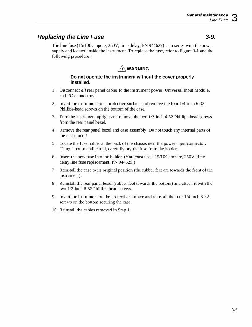
General MaintenanceLine Fuse 3
3-5
Replacing the Line Fuse 3-9.The line fuse (15/100 ampere, 250V, time delay, PN 944629) is in series with the powersupply and located inside the instrument. To replace the fuse, refer to Figure 3-1 and thefollowing procedure:
WARNING
Do not operate the instrument without the cover properlyinstalled.
1. Disconnect all rear panel cables to the instrument power, Universal Input Module,and I/O connectors.
2. Invert the instrument on a protective surface and remove the four 1/4-inch 6-32Phillips-head screws on the bottom of the case.
3. Turn the instrument upright and remove the two 1/2-inch 6-32 Phillips-head screwsfrom the rear panel bezel.
4. Remove the rear panel bezel and case assembly. Do not touch any internal parts ofthe instrument!
5. Locate the fuse holder at the back of the chassis near the power input connector.Using a non-metallic tool, carefully pry the fuse from the holder.
6. Insert the new fuse into the holder. (You must use a 15/100 ampere, 250V, timedelay line fuse replacement, PN 944629.)
7. Reinstall the case to its original position (the rubber feet are towards the front of theinstrument).
8. Reinstall the rear panel bezel (rubber feet towards the bottom) and attach it with thetwo 1/2-inch 6-32 Phillips-head screws.
9. Invert the instrument on the protective surface and reinstall the four 1/4-inch 6-32screws on the bottom securing the case.
10. Reinstall the cables removed in Step 1.
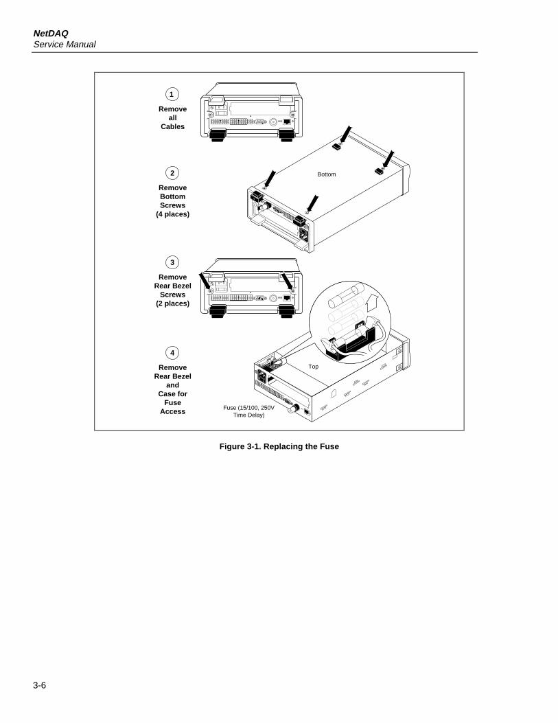
NetDAQService Manual
3-6
1
Removeall
Cables
2
RemoveBottomScrews
(4 places)
3
RemoveRear Bezel
Screws(2 places)
4
RemoveRear Bezel
andCase for
FuseAccess Fuse (15/100, 250V
Time Delay)
Bottom
Top
Figure 3-1. Replacing the Fuse
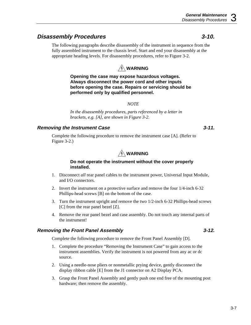
General MaintenanceDisassembly Procedures 3
3-7
Disassembly Procedures 3-10.The following paragraphs describe disassembly of the instrument in sequence from thefully assembled instrument to the chassis level. Start and end your disassembly at theappropriate heading levels. For disassembly procedures, refer to Figure 3-2.
WARNING
Opening the case may expose hazardous voltages.Always disconnect the power cord and other inputsbefore opening the case. Repairs or servicing should beperformed only by qualified personnel.
NOTE
In the disassembly procedures, parts referenced by a letter inbrackets, e.g. [A], are shown in Figure 3-2.
Removing the Instrument Case 3-11.
Complete the following procedure to remove the instrument case [A]. (Refer toFigure 3-2.)
WARNING
Do not operate the instrument without the cover properlyinstalled.
1. Disconnect all rear panel cables to the instrument power, Universal Input Module,and I/O connectors.
2. Invert the instrument on a protective surface and remove the four 1/4-inch 6-32Phillips-head screws [B] on the bottom of the case.
3. Turn the instrument upright and remove the two 1/2-inch 6-32 Phillips-head screws[C] from the rear panel bezel [Z].
4. Remove the rear panel bezel and case assembly. Do not touch any internal parts ofthe instrument!
Removing the Front Panel Assembly 3-12.
Complete the following procedure to remove the Front Panel Assembly [D].
1. Complete the procedure “Removing the Instrument Case” to gain access to theinstrument assemblies. Verify the instrument is not powered from any ac or dcsource.
2. Using a needle-nose pliers or nonmetallic prying device, gently disconnect thedisplay ribbon cable [E] from the J1 connector on A2 Display PCA.
3. Grasp the Front Panel Assembly and gently push one end free of the mounting posthardware; then remove the assembly.
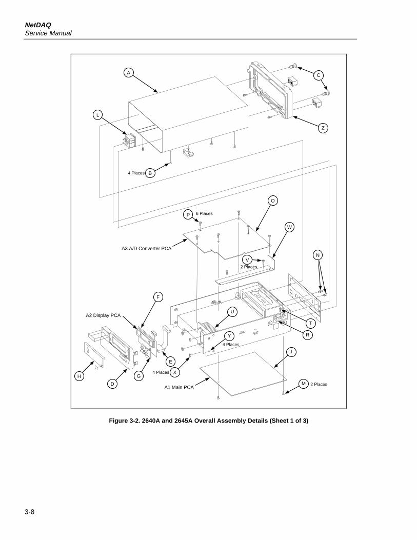
NetDAQService Manual
3-8
L
Z
B
C
4 Places
A
P 6 Places
A3 A/D Converter PCA
O
W
V2 Places
N
T
R
A1 Main PCAM
I
2 Places
U
Y
4 Places
X4 Places
D
H G
E
A2 Display PCA
F
Figure 3-2. 2640A and 2645A Overall Assembly Details (Sheet 1 of 3)
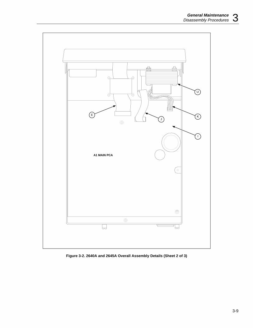
General MaintenanceDisassembly Procedures 3
3-9
EJ
U
K
I
A1 MAIN PCA
Figure 3-2. 2640A and 2645A Overall Assembly Details (Sheet 2 of 3)
NetDAQService Manual
3-10
U
R
S
S
T
J
A3 A/D CONVERTER PCA
Q
L
3 Places
Figure 3-2. 2640A and 2645A Overall Assembly Details (Sheet 3 of 3)
General MaintenanceDisassembly Procedures 3
3-11
Disassembling the Front Panel Assembly 3-13.
Complete the following procedure to disassemble the Front Panel Assembly [D].
1. Place the Front Panel Assembly on a protective surface to prevent any scratching ordamage to the assembly.
2. Release the tabs at the sides and top that hold the A2 Display PCA [F] on the back ofthe Front Panel Assembly; then lift the pca out of its securing slots.
NOTE
The Display PCA provides space for securing screws, which areused only if one or more tabs are broken. If the pca has one or moresecuring screws, remove these as well.
3. To remove the elastomeric keypad [G], grasp the keypad and with a gentle motionpull the keypad free of the assembly.
4. To remove the display window [H], release the two snaps along the bottom edge andpush the window free of the assembly.
CAUTION
Avoid using ammonia or methyl-alcohol cleaning agentson either the Front Panel or the display window. Thesetypes of cleaners can damage surface features andmarkings. Use an isopropyl-based cleaning agent orwater to clean the Front Panel and the display window.
Removing the A1 Main PCA 3-14.
Complete the following procedure to remove the A1 Main PCA [I] from the chassis.
1. Complete the procedure “Removing the Instrument Case” to gain access to theinstrument assemblies. Verify the instrument is not powered from any ac or dcsource.
2. Using a needle-nose pliers or nonmetallic prying device, gently disconnect thedisplay ribbon cable [E] from the connector A1J2.
3. Disconnect the pendant A/D ribbon cable [J] at the A3 A/D Converter PCAconnector A3J10 and gently pull the cable and connector through the chassisopening.
4. Disconnect the transformer cable at A1J3 [K].
5. Using a needle-nose pliers or nonmetallic prying device, remove the two terminalswith red wires from the instrument power switch [L] and gently pull the wires andterminals through the pca opening. (At the power switch, you may find it necessaryto remove the power input terminals to gain access to the red wires. Note the colorand routing of the power input terminals for the reconnection procedure.)
6. Remove the two screws [M] that secure the pca to the chassis.
7. Remove the RS-232 connector hardware [N] using a 3/16-inch nut driver.
8. Slide the pca towards the front of the instrument so that the pca edge indentationsmatch the guide tabs on each side of the chassis, tilt slightly upwards and remove.
NetDAQService Manual
3-12
Removing the A2 Display PCA 3-15.
To remove the A2 Display PCA [F], see the procedure “Disassembling the Front PanelAssembly.”
Removing the A3 A/D Converter PCA 3-16.
Complete the following procedure to remove the A3 A/D Converter PCA [O] from thechassis.
1. Complete the procedure “Removing the Instrument Case” to gain access to theinstrument assemblies. Verify the instrument is not powered from any ac or dcsource.
2. Disconnect the ribbon cable [J] at connector A3J10 that leads to the A1 Main PCA.
3. Remove the six screws [P] that secure the pca to the chassis.
4. Slide the pca towards the front of the instrument so that the pca edge indentationsmatch the guide tabs on each side of the chassis, tilt slightly upwards and remove.(Be sure the Universal Input Module is not connected at the rear panel.)
Removing the A4 Analog Input PCA 3-17.
Complete the following procedure to remove the A4 Analog Input PCA from theUniversal Input Module.
1. Remove the Universal Input Module from the instrument. Open the module anddisconnect all inputs to the terminal strips.
2. Using a nonmetallic prying device, widen the side of the module next to one of thesecuring tabs (located near the ends of the terminal strips), and pry one edge of thepca free of the module. Lift the free edge of the pca upwards and remove from themodule.
Removing Miscellaneous Chassis Components 3-18.
Complete the following procedure to remove miscellaneous chassis components,including the power switch/input connector, fuseholder, and power transformer.
Removing the Power Switch/Input Connector 3-19.
Complete the following procedure to remove the power switch/input connector [L].
1. Complete the procedure “Removing the Instrument Case” to gain access to theinstrument assemblies. Verify the instrument is not powered from any ac or dcsource.
2. Disconnect all five terminals [Q] from the power switch/input connector.
3. Compress the tab at one side of the power switch/input connector and partiallyremove the switch from the chassis. Repeat for the other tab and remove the switchfrom the chassis.
General MaintenanceAssembly Procedures 3
3-13
Removing the Fuseholder 3-20.
Complete the following procedure to remove the fuseholder [R].
1. Complete the procedure “Removing the Instrument Case” to gain access to theinstrument assemblies. Verify the instrument is not ac or dc powered.
2. Remove the fuse from the fuseholder.
3. Disconnect the two terminals [S] from the fuseholder.
4. Remove the single screw [T] securing the fuseholder.
Removing the Power Transformer 3-21.
Complete the following procedure to remove the power transformer [U].
1. Remove the A3 A/D Converter PCA. (See the procedure “Removing the A3 A/DConverter PCA.”)
2. Disconnect the white wire (blue wire on early production units) that leads to thetransformer at the input connector.
3. Disconnect the black wire (brown wire on early production units) that leads to thetransformer at the fuseholder.
4. Disconnect the transformer connection at A1J3 [K] on the A1 Main PCA.
5. Remove the two screws [V] that secure the transformer wire cover plate [W] andside the plate free from the chassis and remove.
6. Remove the four nuts [X] that secure the transformer to the chassis mounting plate.
Assembly Procedures 3-22.The following paragraphs describe assembly of the instrument in sequence from the fullyunassembled instrument. Start and end your disassembly at the appropriate headinglevels. For assembly procedures, refer to Figure 3-2 as required.
NOTE
In the assembly procedures, parts referenced by a letter in brackets,e.g. [A], are shown in Figure 3-2.
Installing Miscellaneous Chassis Components 3-23.
Complete the following procedure to install miscellaneous chassis components,including the power switch/input connector, fuseholder, and power transformer. Refer toFigure 3-2 and 3-3 as required.
Installing the Power Transformer 3-24.
Complete the following procedure to install the power transformer [U].
1. Install the four nuts [X] that secure the transformer to the chassis mounting plate.
2. Route the twisted white and brown wires to the fuseholder area; then install the twoscrews [V] that secure the transformer wire cover plate [W].
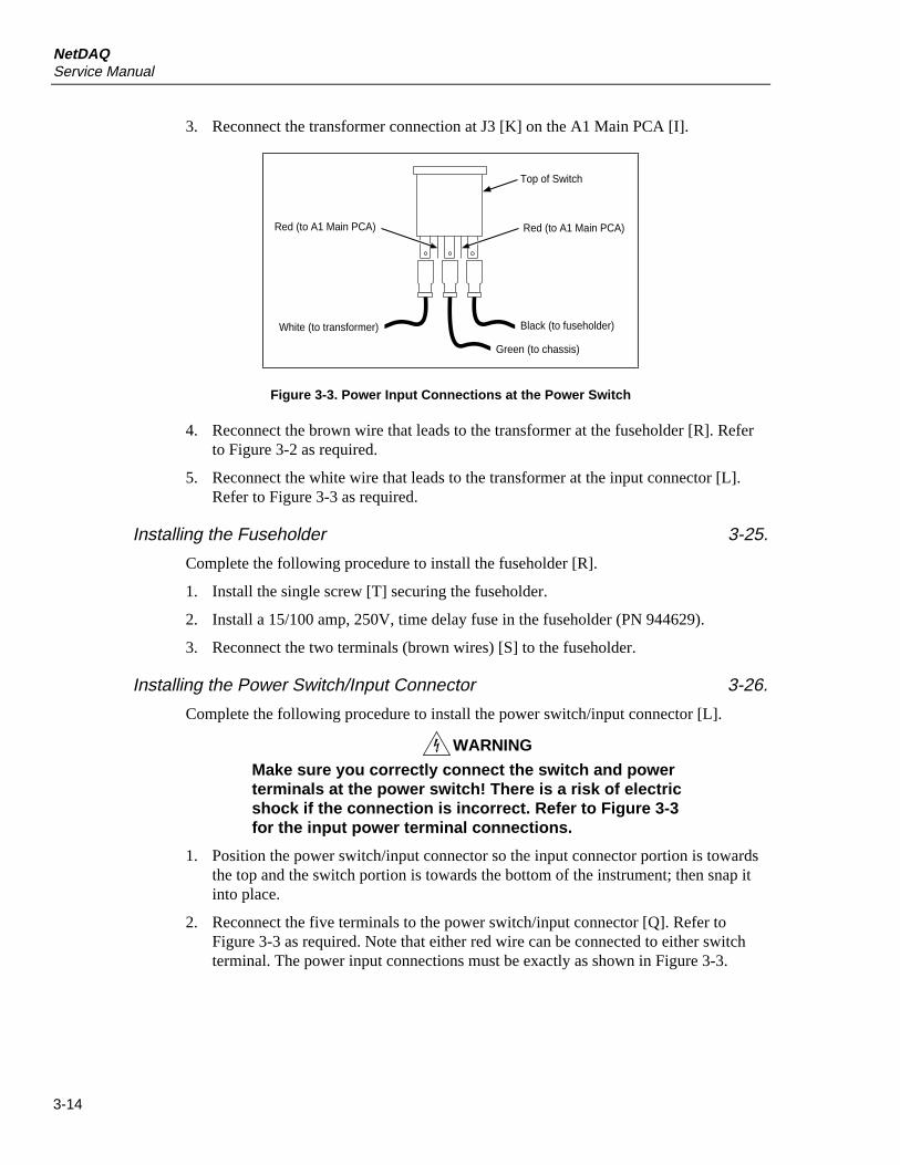
NetDAQService Manual
3-14
3. Reconnect the transformer connection at J3 [K] on the A1 Main PCA [I].
White (to transformer)
Red (to A1 Main PCA) Red (to A1 Main PCA)
Top of Switch
Black (to fuseholder)
Green (to chassis)
Figure 3-3. Power Input Connections at the Power Switch
4. Reconnect the brown wire that leads to the transformer at the fuseholder [R]. Referto Figure 3-2 as required.
5. Reconnect the white wire that leads to the transformer at the input connector [L].Refer to Figure 3-3 as required.
Installing the Fuseholder 3-25.
Complete the following procedure to install the fuseholder [R].
1. Install the single screw [T] securing the fuseholder.
2. Install a 15/100 amp, 250V, time delay fuse in the fuseholder (PN 944629).
3. Reconnect the two terminals (brown wires) [S] to the fuseholder.
Installing the Power Switch/Input Connector 3-26.
Complete the following procedure to install the power switch/input connector [L].
WARNING
Make sure you correctly connect the switch and powerterminals at the power switch! There is a risk of electricshock if the connection is incorrect. Refer to Figure 3-3for the input power terminal connections.
1. Position the power switch/input connector so the input connector portion is towardsthe top and the switch portion is towards the bottom of the instrument; then snap itinto place.
2. Reconnect the five terminals to the power switch/input connector [Q]. Refer toFigure 3-3 as required. Note that either red wire can be connected to either switchterminal. The power input connections must be exactly as shown in Figure 3-3.
General MaintenanceAssembly Procedures 3
3-15
Installing the A1 Main PCA 3-27.
Complete the following procedure to install the A1 Main PCA [I].
1. Tilt the rear portion of the pca slightly downwards and position the pca in thechassis. Slide the pca towards the rear and into position.
2. Install the RS-232 connector hardware [N] at the rear panel using a 3/16-inch nutdriver.
3. Install the two screws [M] that secure the pca to the chassis.
WARNING
Make sure you correctly connect the switch and powerterminals at the power switch! There is a risk of electricshock if the connection is incorrect. Refer to Figure 3-3for the input power terminal connections.
4. Thread the two red wires through the pca and connect to the power switch. Either redwire can be connected to either switch terminal. Do not accidentally connect the redwires to any input power terminal! (If you removed the power input terminals,reconnect them as shown in Figure 3-3.)
5. Reconnect the transformer cable at A1J3.
6. Route the pendant A/D ribbon cable [J] (from A1P10) through the chassis openingand reconnect it to the A3 A/D Converter PCA connector A3J10.
7. Gently reconnect the display ribbon cable [E] to the connector A1J2.
8. Complete the procedure “Installing the Instrument Case,” as required.
Installing the A2 Display PCA 3-28.
To install the A2 Display PCA, see “Assembling the Front Panel Assembly.”
Installing the A3 A/D Converter PCA 3-29.
Complete the following procedure to install the A3 A/D Converter PCA [O].
1. Tilt the rear portion of the pca slightly downwards and position the pca in thechassis. Slide the pca towards the rear and into position.
2. Install the six screws [P] that secure the pca to the chassis.
3. Reconnect the ribbon cable [J] at connector A3J10 that leads to A1P10 on the A1Main PCA.
4. Complete the procedure “Installing the Instrument Case,” as required.
Installing the A4 Analog Input PCA 3-30.
Complete the following procedure to install the A4 Analog Input PCA.
1. Place the pca in position in the module.
2. Widen a side of the module next to one of the securing tabs (located near the ends ofthe terminal strips), and press the pca firmly into place. Repeat for the other tab.
3. Reconnect the input measurement wires, as required.
NetDAQService Manual
3-16
Assembling the Front Panel Assembly 3-31.
Complete the following procedure to assemble the Front Panel Assembly [D].
1. Place the Front Panel Assembly on a protective surface to prevent any scratching ordamage to the assembly.
2. Position the display window [H] in place; then push it firmly to snap it into positionin the assembly.
3. Position the elastomeric keypad [G] in place; then gently press it into position in theassembly.
4. Position the A2 Display PCA [F] in place; then push it firmly to snap it into positionin the assembly. It may be necessary to slightly distend the top of the bezel to allowthe pca to snap into position.
NOTE
The Display PCA provides space for securing screws, which areused only if one or more tabs are broken. If the pca uses one ormore securing screws, install these as well.
CAUTION
Avoid using ammonia or methyl-alcohol cleaning agentson either the Front Panel or the display window. Thesetypes of cleaners can damage surface features andmarkings. Use an isopropyl-based cleaning agent orwater to clean the Front Panel and the display window.
Installing the Front Panel Assembly 3-32.
Complete the following procedure to install the Front Panel Assembly [D]:
1. Gently connect the display ribbon cable [E] to the connector on A2 Display PCA.
2. Position the Front Panel Assembly on the chassis mounting post hardware [Y].
3. Complete the procedure “Installing the Instrument Case,” as required.
Installing the Instrument Case 3-33.
Complete the following procedure to install the instrument case [A]. (Refer toFigure 3-2.)
WARNING
Do not operate the instrument without the cover properly installed.
1. Reinstall the case to its original position (the rubber feet are towards the front of theinstrument).
2. Reinstall the rear panel bezel (rubber feet towards the bottom) [Z] and attach it withthe two 1/2-inch 6-32 Phillips-head screws [C].
3. Invert the instrument on the protective surface and reinstall the four 1/4-inch 6-32screws [B] on the bottom securing the case.
4. Reinstall the measurement connection cables and power cord, as required.
4-1
Chapter 4Performance Testing and Calibration
Title Page
4-1. Introduction ............................................................................................ 4-34-2. Performance Test.................................................................................... 4-34-3. Configuring the Performance Test Setup........................................... 4-34-4. Initializing the Performance Test Setup ............................................ 4-64-5. Accuracy Performance Tests ............................................................. 4-74-6. Volts DC Accuracy Test (2640A) ................................................. 4-84-7. Volts DC Accuracy Test (2645A) ................................................. 4-94-8. Volts AC Accuracy Test................................................................ 4-104-9. Frequency Accuracy Test .............................................................. 4-104-10. Analog Channel Integrity Test ...................................................... 4-114-11. Computed Channel Integrity Test ................................................. 4-114-12. Thermocouple Temperature Accuracy Test .................................. 4-124-13. Open Thermocouple Response Test .............................................. 4-124-14. Two-Terminal Resistance Accuracy Test (2640A)....................... 4-134-15. Two-Terminal Resistance Accuracy Test (2645A)....................... 4-144-16. Four-Terminal Resistance Accuracy Test (2640A)....................... 4-154-17. Four-Terminal Resistance Accuracy Test (2645A)....................... 4-174-18. RTD Temperature Accuracy Test (Resistance) (2640A) .............. 4-184-19. RTD Temperature Accuracy Test (Resistance) (2645A) .............. 4-194-20. RTD Temperature Accuracy Test (DIN/IEC 751 RTD) ............... 4-194-21. Digital Input/Output Tests ................................................................. 4-204-22. Digital I/O Output Test.................................................................. 4-204-23. Digital Input Test........................................................................... 4-214-24. Totalizer Tests.................................................................................... 4-224-25. Totalizer Count Test ...................................................................... 4-224-26. Totalizer Sensitivity Test............................................................... 4-234-27. Master Alarm Output Test ................................................................. 4-234-28. Trigger Input Test .............................................................................. 4-244-29. Trigger Output Test............................................................................ 4-24
NetDAQService Manual
4-2
4-30. Calibration.............................................................................................. 4-254-31. Methods of Calibration ...................................................................... 4-254-32. Preparing for Calibration ................................................................... 4-264-33. Ending Calibration ............................................................................. 4-284-34. RS-232 Instrument Configuration Parameters................................... 4-284-35. Calibration Procedure (Automatic).................................................... 4-284-36. Calibration Procedure (Semiautomatic) ............................................ 4-284-37. VDC Calibration Procedure........................................................... 4-314-38. VAC Calibration Procedure........................................................... 4-324-39. Resistance Calibration Procedure.................................................. 4-334-40. Frequency Calibration Procedure .................................................. 4-344-41. Calibration Procedure (Manual) ........................................................ 4-344-42. Manual Calibration Commands..................................................... 4-364-43. Manual VDC Calibration Procedure ............................................. 4-374-44. Manual VAC Calibration Procedure ............................................. 4-384-45. Manual Resistance Calibration Procedure..................................... 4-394-46. Manual Frequency Calibration Procedure..................................... 4-41
Performance Testing and CalibrationIntroduction 4
4-3
Introduction 4-1.This section of the Service Manual provides performance tests that are used at any timeto verify that the operation of the instrument networked data acquisition units (2640A or2645A) is within published specifications. A complete calibration procedure is alsoincluded. The performance test and, if necessary, the calibration procedures areperformed periodically as well as after service or repair.
Performance Test 4-2.When received, the 2640A/2645A is calibrated and in operating condition. Thefollowing Performance Test procedures are provided for acceptance testing upon initialreceipt or to verify correct instrument operation. The performance tests must beperformed in sequence.
If the instrument fails a performance test, the instrument requires service or repair. Toperform these tests, you will need a Fluke 5700A Multifunction Calibrator and severalother pieces of equipment that meet the minimum specifications given in Table 4-1.
Each of the measurements listed in the following steps assume the instrument is beingtested after a 1/2 hour warm-up, in an environment with an ambient temperature of 18 to28°C, and a relative humidity of less than 70%.
WARNING
The 2640A/2645A instruments contain high voltages that aredangerous or fatal. Only qualified personnel should attempt toservice the instruments.
Configuring the Performance Test Setup 4-3.
Configure the performance test setup as described below. The performance test requiresa complete network connection between the host computer and instrument under test,including a host computer Ethernet interface and installation of NetDAQ Logger forWindows software. If you have not yet configured and tested a network connection forthe host computer and instrument, complete the appropriate installation procedure foryour network configuration in the separate NetDAQ Getting Started manual beforeconducting any performance testing.
1. Connect the Instrument and the Host Computer Connect the supplied 50-ohmcoaxial cable, with a BNC "T" or "Y" and 50-ohm terminator, between the hostcomputer BNC Ethernet port and the instrument BNC Ethernet port. The 50-ohmterminator with the ground lead is used at the instrument with the terminator groundlug connected to the ground terminal adjacent to the BNC port (Figure 4-1).
2. Connect the 5700A to Channel 1 Connect a cable from the Output VA HI and LOconnectors of the 5700A to the Universal Input Module terminals for channel 1connecting the 5700A HI to terminal H and LO to terminal L. Insert the UniversalInput Module into the instrument under test (Figure 4-2).
NetDAQService Manual
4-4
Table 4-1. Recommended Test Equipment
Instrument Type Minimum Specifications Recommended Model
Multifunction DC Voltage: Fluke 5700A
Calibrator Range: 90 mV to 300V dc
Accuracy: 0.002%
AC Voltage:
Frequency Voltage Accuracy
1 kHz 29 mV to 300V 0.05%
100 kHz 15 mV to 300V 0.5%
Frequency:
10 kHz 1V rms 0.01%
Ohms:
Ohms Accuracy
190Ω 0.005%
1.9 kΩ 0.005%
19 kΩ 0.005%
190 kΩ 0.005%
1.9 MΩ 0.005%
Mercury Thermometer 0.02°C Resolution Princo ASTM-56C
Thermocouple Probe Type T Fluke P20T
Oil/Water Bath Thermos bottle and cap
Digital Multimeter General Purpose Measurement Fluke 77
Signal Generator Sine wave. 0.5 to 1V rms, 10 Hz to 5 kHz Fluke 6011A
Alternative Equipment List
Instrument Type Recommended Model
DC Voltage Calibrator Fluke 5440B
DMM Calibrator Fluke 5100B (AC Volts Only)
Function/Signal Generator Philips PM5193 or Fluke 6011A
Decade Resistance Source General Resistance RDS 66A
Performance Testing and CalibrationPerformance Test 4
4-5
Instrument
HostComputer
50-ohmTerminator
Ethernet Coaxial Cable (50-ohm)
Minimum cable lengthis 20 inches (0.5 m).
50-ohmTerminator
COMM DIO MON
ENTER
BNC “T”
Terminator Ground Wire
NetDAQNETWORKED DATA ACQUISITION UNIT
FIGURE 4-1. Performance Test Setup
1211 13 14 15 16 17 18 19 20
21 3 4 5 6 7 8 9 10
SOURCE(4-WIRE)
SENSE(4-WIRE)
H L H L H L H L H L H L H L H L H L H L
H L H L H L H L H L H L H L H L H L
INPUTMODULE
HI HI
LO LO
HI
OUTPUTV A
SENSEV
AUXCURRENT
GUARD GROUND
WIDEBAND
Ω Ω
5700A
H L
Figure 4-2. Two-Terminal Connections to 5700A
NetDAQService Manual
4-6
Initializing the Performance Test Setup 4-4.
Complete the following procedure to initialize the performance test setup. It is assumedyou have configured the host computer and instrument as described in "Configuring thePerformance Test Setup" (above). Testing begins with the instrument and host computerunpowered. This assures that at power-up, self-tests are completed successfully, thecorrect host computer Ethernet port is activated, the host computer configuration isaccurately reflected, and other background operations are completed. This procedureclears the instrument of any existing BCN, Line Frequency, and Network settings.
1. Apply Instrument Power with Configuration Reset Hold down the COMM keyon the instrument front panel and apply power to the instrument. After theinstrument beeps and momentarily displays "rESEt" (Reset), release the COMM key.If any self-test errors are reported on the front panel display, refer to "Self-TestDiagnostics and Error Codes" in this chapter. Configuration Reset sets theinstrument to the default parameters: BCN=1, Line Frequency=60, and IsolatedNetwork.
2. Set the Line Frequency If the ac power applied to your instrument is 60 Hz(default), continue to Step 3. If the ac power applied to your instrument is 50 Hz,complete this step.
Press the COMM key for 3 seconds, until your hear a beep and the SET annunciatorin the display lights. Press the up/down arrow keys until LinE (Line Frequency) isdisplayed in the primary display. Press the ENTER key. Press the up/down arrowkeys until 50 (50 Hz) is displayed in the primary display. Press the ENTER key.
3. Apply Host Computer Power Apply power to the host computer.
4. Open NetDAQ Logger for Windows Open NetDAQ Logger from the FlukeNetDAQ Logger group in Program Manager.
5. Add Instrument Select the Communications Config command from the Setupmenu to open the Communications Configuration File dialog box. If the command isdimmed, Configuration Lockout is checked in the Options menu. Observe theInstruments on Network list. If the list includes instrument 01 with the correct modelnumber (model 2640A or model 2645A), continue to Step 6.
If instrument 01 is listed but with the wrong model number, select (highlight) theinstrument on the Instruments on Network list and click the Modify button. Selectthe correct model and click OK. If instrument 01 is not listed, click the Add buttonand add instrument 01 with the correct model number. Click OK.
6. Verify Communications. With the Communications Configuration File dialog boxstill open, select instrument 01 on the Instruments on Network list and click theVerify button. The message Connection Successful! is returned for a successfulcommunications between the instrument and host computer. If you receive an errormessage, refer to "Error and Status Messages" in Chapter 4. Click OK in themessage box and then the Close button in the Communications Configuration Filedialog box to return to the Main Window.
Performance Testing and CalibrationPerformance Test 4
4-7
7. Configure Icon Note the Icon Bar in the Main Window. If the Icon Bar showsinstrument 01, complete Reset Instrument Icon below. If the Icon Bar does not showinstrument 01, complete Create Instrument Icon below.
Reset Instrument Icon Select the Delete Instrument Icon form the Setup menu. If thecommand is dimmed, Configuration Lockout is checked in the Options menu. ClickYes in warning message. Complete Create Instrument Icon below. (This sequenceclears all configuration data from the instrument.)
Create Instrument Icon Select the Create Instrument Icon from the Setup menu. Ifthe command is dimmed, Configuration Lockout is checked in the Options menu.Select instrument 01 on the Available Instruments List. Click OK.
8. Select Reading Rate and Trigger Out Click the Instrument Config button on theButton Bar, opening the Instrument Configuration dialog box. Select Reading Rate =Slow, and check the Trigger Out box. Click OK to return to the Main Window.
9. Connect DIGITAL I/O Test Leads Remove the 10-position DIGITAL I/Oconnector from the instrument rear panel or from the connector kit supplied with theinstrument. Connect a test lead to each DIO line 0 to 7, plus a test lead to the Σ(Totalizer) input and the common GND line. Reinstall the DIGITAL I/O connector.
10. Connect ALARM/TRIGGER I/O Test Leads Remove the 8-positionALARM/TRIGGER I/O connector from the instrument rear panel or from theconnector kit supplied with the instrument. Connect a test lead to each line, MA(Master Alarm), TO (Trigger Output), TI (Trigger Input), plus a test lead to thecommon GND line.
Accuracy Performance Tests 4-5.
This accuracy performance test assumes you have completed "Initializing thePerformance Test Setup" above. Do not begin this test until the instrument hastemperature stabilized for a minimum of 30 minutes. Do not use the instrument frontpanel monitor function for performance testing; use the higher resolution Spy window atthe host computer as specified in the procedures. The Accuracy Performance Testsinclude the following:
• Volts DC Accuracy Test
• Volts AC Accuracy Test
• Frequency Accuracy Test
• Analog Channel Integrity Test
• Computed Channel Integrity Test
• Thermocouple Temperature Accuracy Test
• Open Thermocouple Response Test
• Two-Terminal Resistance Accuracy Test
• Four-Terminal Resistance Accuracy Test
• RTD Temperature Accuracy Test (Resistance Source)
• RTD Temperature Accuracy Test (DIN/IEC 751 RTD Source)
Tests for current dc are not included since these functions are derived from volts dc.
NetDAQService Manual
4-8
Volts DC Accuracy Test (2640A) 4-6.
Complete the following procedure to test the accuracy of the volts dc function for the2640A. Measurement accuracy applies to all channels, not just the channel used for thetest.
1. Configure Channel 1 for Volts DC In NetDAQ Logger for Windows, configurechannel 1 for volts dc, 90 mV range.
2. Open Spy Window Select the Spy command from the Utilities menu. Selectchannel 0101 (instrument 01, channel 01) from the Channel list. Click OK to openthe Spy window.
3. Verify Accuracy Configure the 5700A for the output values below and verify theSpy window measurement is between the minimum and maximum values. Changethe channel 1 range as required (see Step 1).
Volts DC Range 5700A Output Minimum Reading Maximum Reading
90 mV Short Circuit (Zero) -0.000008V +0.000008V
90 mV +90 mV +0.089980V +0.090020V
90 mV -90 mV -0.090020V -0.089980V
300 mV Short Circuit (Zero) -0.000017V +0.000017V
300 mV +300 mV +0.299944V +0.300056V
300 mV -300 mV -0.300056V -0.299944V
3V Short Circuit (Zero) -0.00015V +0.00015V
3V +3V +2.99946V +3.00054V
3V -3V -3.00054V -2.99946V
30V Short Circuit (Zero) -0.0017V +0.0017V
30V +30V +29.9944V +30.0056V
30V -30V -30.0056V -29.9944V
300V Short Circuit (Zero) -0.017V +0.017V
300V +300V +299.944V +300.056V
300V -300V -300.056V -299.944V
4. Close Spy Window To close the Spy window, double-click the upper left-handcorner control-menu box.
Performance Testing and CalibrationPerformance Test 4
4-9
Volts DC Accuracy Test (2645A) 4-7.
Complete the following procedure to test the accuracy of the volts dc function for the2645A. Measurement accuracy applies to all channels, not just the channel used for thetest.
1. Configure Channel 1 for Volts DC In NetDAQ Logger for Windows, configurechannel 1 for volts dc, 90 mV range.
2. Open Spy Window Select the Spy command from the Utilities menu. Selectchannel 0101 (instrument 01, channel 01) from the Channel list. Click OK to openthe Spy window.
3. Verify Accuracy Configure the 5700A for the output values below and verify theSpy window measurement is between the minimum and maximum values. Changethe channel 1 range as required (see Step 1).
Volts DC Range 5700A Output Minimum Reading Maximum Reading
90 mV Short Circuit (Zero) -0.000023V +0.000023V
90 mV +90 mV +0.089965V +0.090035V
90 mV -90 mV -0.090035V -0.089965V
300 mV Short Circuit (Zero) -0.00005V +0.00005V
300 mV +300 mV +0.29991V +0.30009V
300 mV -300 mV -0.30009V -0.29991V
3V Short Circuit (Zero) -0.0004V +0.0004V
3V +3V +2.9992V +3.0008V
3V -3V -3.0008V -2.9992V
30V Short Circuit (Zero) -0.005V +0.005V
30V +30V +29.991V +30.009V
30V -30V -30.009V -29.991V
50V Short Circuit (Zero) -0.04V +0.04V
50V +50V +49.95V +50.05V
50V -50V -50.05V -49.95V
4. Close Spy Window To close the Spy window, double-click the upper left-handcorner control-menu box.
NetDAQService Manual
4-10
Volts AC Accuracy Test 4-8.
Complete the following procedure to test the accuracy of the volts ac function for boththe 2640A and 2645A. Measurement accuracy applies to all channels, not just thechannel used for the test.
1. Configure Channel 1 for Volts AC In NetDAQ Logger for Windows, configurechannel 1 for volts ac, 300 mV range.
2. Open Spy Window Select the Spy command from the Utilities menu. Selectchannel 0101 (instrument 01, channel 01) from the Channel list. Click OK to openthe Spy window.
3. Verify Accuracy Configure the 5700A for the output values below and verify theSpy window measurement is between the minimum and maximum values. Changethe channel 1 range as required (see Step 1).
Volts AC Range 5700A Output Minimum Reading Maximum Reading
300 mV 20 mV@1 kHz 0.0197V 0.0203V
300 mV 20 mV@100kHZ 0.0185V 0.0215V
300 mV 300 mV@1 kHz 0.29885V 0.30115V
300 mV 300 mV@100 kHz 0.2845V 0.3155V
3V 3V@1 kHz 2.9885V 3.0115V
30V 30V@1 kHz 29.885V 30.115V
300V [2640A only] 300V@1 kHz 298.85V 301.15V
4. Close Spy Window To close the Spy window, double-click the upper left-handcorner control-menu box.
Frequency Accuracy Test 4-9.
Complete the following procedure to test the accuracy of the frequency function for the2640A and 2645A. Measurement accuracy applies to all channels, not just the channelused for the test.
1. Configure Channel 1 for Frequency In NetDAQ Logger for Windows, configurechannel 1 for frequency. There is no range selection for frequency because allfrequency measurements use Autoranging.
2. Open Spy Window Select the Spy command from the Utilities menu. Selectchannel 0101 (instrument 01, channel 01) from the Channel list. Click OK to openthe Spy window.
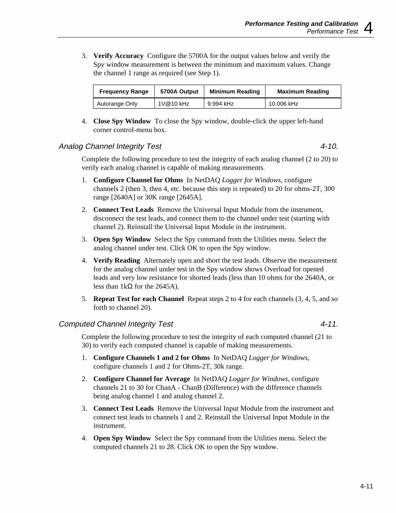
Performance Testing and CalibrationPerformance Test 4
4-11
3. Verify Accuracy Configure the 5700A for the output values below and verify theSpy window measurement is between the minimum and maximum values. Changethe channel 1 range as required (see Step 1).
Frequency Range 5700A Output Minimum Reading Maximum Reading
Autorange Only 1V@10 kHz 9.994 kHz 10.006 kHz
4. Close Spy Window To close the Spy window, double-click the upper left-handcorner control-menu box.
Analog Channel Integrity Test 4-10.
Complete the following procedure to test the integrity of each analog channel (2 to 20) toverify each analog channel is capable of making measurements.
1. Configure Channel for Ohms In NetDAQ Logger for Windows, configurechannels 2 (then 3, then 4, etc. because this step is repeated) to 20 for ohms-2T, 300range [2640A] or 30K range [2645A].
2. Connect Test Leads Remove the Universal Input Module from the instrument,disconnect the test leads, and connect them to the channel under test (starting withchannel 2). Reinstall the Universal Input Module in the instrument.
3. Open Spy Window Select the Spy command from the Utilities menu. Select theanalog channel under test. Click OK to open the Spy window.
4. Verify Reading Alternately open and short the test leads. Observe the measurementfor the analog channel under test in the Spy window shows Overload for openedleads and very low resistance for shorted leads (less than 10 ohms for the 2640A, orless than 1kΩ for the 2645A).
5. Repeat Test for each Channel Repeat steps 2 to 4 for each channels (3, 4, 5, and soforth to channel 20).
Computed Channel Integrity Test 4-11.
Complete the following procedure to test the integrity of each computed channel (21 to30) to verify each computed channel is capable of making measurements.
1. Configure Channels 1 and 2 for Ohms In NetDAQ Logger for Windows,configure channels 1 and 2 for Ohms-2T, 30k range.
2. Configure Channel for Average In NetDAQ Logger for Windows, configurechannels 21 to 30 for ChanA - ChanB (Difference) with the difference channelsbeing analog channel 1 and analog channel 2.
3. Connect Test Leads Remove the Universal Input Module from the instrument andconnect test leads to channels 1 and 2. Reinstall the Universal Input Module in theinstrument.
4. Open Spy Window Select the Spy command from the Utilities menu. Select thecomputed channels 21 to 28. Click OK to open the Spy window.
NetDAQService Manual
4-12
5. Verify Reading Alternately open and short both sets of test leads. Observe themeasurement for the computed channel under test in the Spy window shows+Overload for opened leads and very low resistance for shorted leads.
6. Repeat Test Repeat steps 4 to 5 for channels 29 and 30.
Thermocouple Temperature Accuracy Test 4-12.
Ensure that the Accuracy Tests (above) have been completed before performing this test.
1. Connect a Thermocouple Remove the Universal Input Module from the instrumentand connect the supplied type T thermocouple to the channel 1 terminals with theblue lead to the H terminal and red lead to the L terminal. Reinstall the UniversalInput Module.
2. Configure Channel 1 for Thermocouples In NetDAQ Logger for Windows,configure channel 1 for Thermocouples with Range (thermocouple type) T.
3. Open Spy Window Select the Spy command from the Utilities menu. Select analogchannel 01. Click OK to open the Spy window.
4. Verify Accuracy Insert the thermocouple and a mercury thermometer in a room-temperature bath. Allow 20 minutes for thermal stabilization. The value displayed onthe mercury thermometer should equal the value in the Spy Window + 0.5°C(2640A) or + 1.0°C (2645A) plus any sensor inaccuracies.
5. Close Spy Window To close the Spy window, double-click the upper left-handcorner control-menu box.
Open Thermocouple Response Test 4-13.
This test checks the Open Thermocouple response.
1. Connect an 820 Ohm Test Resistor Remove the Universal Input Module from theinstrument and connect an 820 ohm resistor to the channel 1 terminals. Reinstall theUniversal Input Module.
2. Configure Channel 1 for Thermocouples In NetDAQ Logger for Windows,configure channel 1 for Thermocouples with Range (thermocouple type) K.
3. Open Spy Window Select the Spy command from the Utilities menu. Select analogchannel 1. Click OK to open the Spy window. The value displayed shouldapproximate the ambient temperature.
4. Connect a 10kΩ Test Resistor Remove the Universal Input Module from theinstrument and connect a 10kΩ resistor to the channel 1 terminals to simulate anopen thermocouple condition. Reinstall the Universal Input Module.
5. Verify Open Thermocouple The Spy window indicates an open thermocoupledetect condition by displaying Open TC in place of a temperature reading.
6. Close Spy Window To close the Spy window, double-click the upper left-handcorner control-menu box.
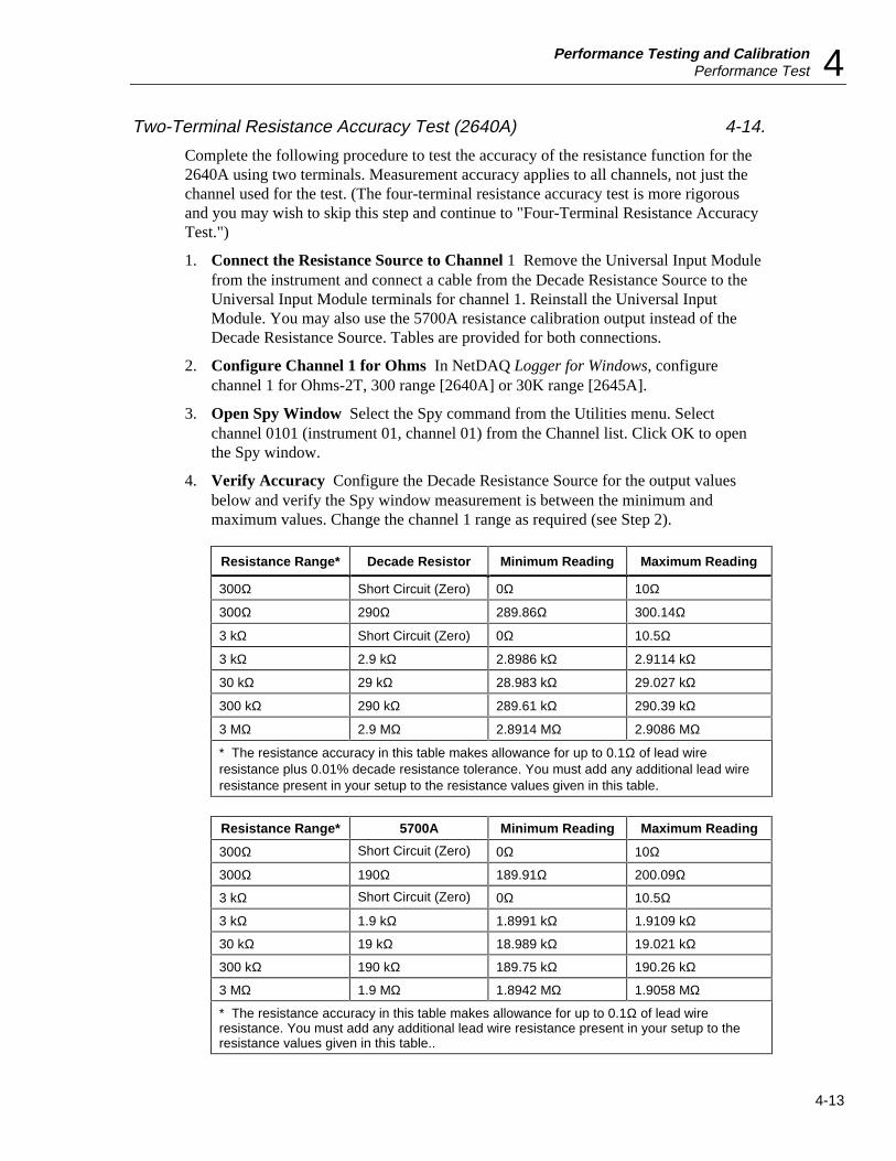
Performance Testing and CalibrationPerformance Test 4
4-13
Two-Terminal Resistance Accuracy Test (2640A) 4-14.
Complete the following procedure to test the accuracy of the resistance function for the2640A using two terminals. Measurement accuracy applies to all channels, not just thechannel used for the test. (The four-terminal resistance accuracy test is more rigorousand you may wish to skip this step and continue to "Four-Terminal Resistance AccuracyTest.")
1. Connect the Resistance Source to Channel 1 Remove the Universal Input Modulefrom the instrument and connect a cable from the Decade Resistance Source to theUniversal Input Module terminals for channel 1. Reinstall the Universal InputModule. You may also use the 5700A resistance calibration output instead of theDecade Resistance Source. Tables are provided for both connections.
2. Configure Channel 1 for Ohms In NetDAQ Logger for Windows, configurechannel 1 for Ohms-2T, 300 range [2640A] or 30K range [2645A].
3. Open Spy Window Select the Spy command from the Utilities menu. Selectchannel 0101 (instrument 01, channel 01) from the Channel list. Click OK to openthe Spy window.
4. Verify Accuracy Configure the Decade Resistance Source for the output valuesbelow and verify the Spy window measurement is between the minimum andmaximum values. Change the channel 1 range as required (see Step 2).
Resistance Range* Decade Resistor Minimum Reading Maximum Reading
300Ω Short Circuit (Zero) 0Ω 10Ω
300Ω 290Ω 289.86Ω 300.14Ω
3 kΩ Short Circuit (Zero) 0Ω 10.5Ω
3 kΩ 2.9 kΩ 2.8986 kΩ 2.9114 kΩ
30 kΩ 29 kΩ 28.983 kΩ 29.027 kΩ
300 kΩ 290 kΩ 289.61 kΩ 290.39 kΩ
3 MΩ 2.9 MΩ 2.8914 MΩ 2.9086 MΩ
* The resistance accuracy in this table makes allowance for up to 0.1Ω of lead wireresistance plus 0.01% decade resistance tolerance. You must add any additional lead wireresistance present in your setup to the resistance values given in this table.
Resistance Range* 5700A Minimum Reading Maximum Reading
300Ω Short Circuit (Zero) 0Ω 10Ω
300Ω 190Ω 189.91Ω 200.09Ω
3 kΩ Short Circuit (Zero) 0Ω 10.5Ω
3 kΩ 1.9 kΩ 1.8991 kΩ 1.9109 kΩ
30 kΩ 19 kΩ 18.989 kΩ 19.021 kΩ
300 kΩ 190 kΩ 189.75 kΩ 190.26 kΩ
3 MΩ 1.9 MΩ 1.8942 MΩ 1.9058 MΩ
* The resistance accuracy in this table makes allowance for up to 0.1Ω of lead wireresistance. You must add any additional lead wire resistance present in your setup to theresistance values given in this table..
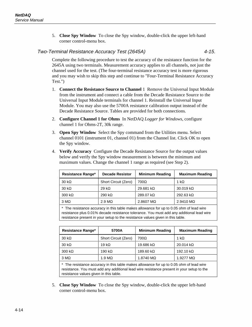
NetDAQService Manual
4-14
5. Close Spy Window To close the Spy window, double-click the upper left-handcorner control-menu box.
Two-Terminal Resistance Accuracy Test (2645A) 4-15.
Complete the following procedure to test the accuracy of the resistance function for the2645A using two terminals. Measurement accuracy applies to all channels, not just thechannel used for the test. (The four-terminal resistance accuracy test is more rigorousand you may wish to skip this step and continue to "Four-Terminal Resistance AccuracyTest.")
1. Connect the Resistance Source to Channel 1 Remove the Universal Input Modulefrom the instrument and connect a cable from the Decade Resistance Source to theUniversal Input Module terminals for channel 1. Reinstall the Universal InputModule. You may also use the 5700A resistance calibration output instead of theDecade Resistance Source. Tables are provided for both connections.
2. Configure Channel 1 for Ohms In NetDAQ Logger for Windows, configurechannel 1 for Ohms-2T, 30k range.
3. Open Spy Window Select the Spy command from the Utilities menu. Selectchannel 0101 (instrument 01, channel 01) from the Channel list. Click OK to openthe Spy window.
4. Verify Accuracy Configure the Decade Resistance Source for the output valuesbelow and verify the Spy window measurement is between the minimum andmaximum values. Change the channel 1 range as required (see Step 2).
Resistance Range* Decade Resistor Minimum Reading Maximum Reading
30 kΩ Short Circuit (Zero) 700Ω 1 kΩ
30 kΩ 29 kΩ 29.681 kΩ 30.019 kΩ
300 kΩ 290 kΩ 289.07 kΩ 292.63 kΩ
3 MΩ 2.9 MΩ 2.8607 MΩ 2.9410 MΩ
* The resistance accuracy in this table makes allowance for up to 0.05 ohm of lead wireresistance plus 0.01% decade resistance tolerance. You must add any additional lead wireresistance present in your setup to the resistance values given in this table.
Resistance Range* 5700A Minimum Reading Maximum Reading
30 kΩ Short Circuit (Zero) 700Ω 1 kΩ
30 kΩ 19 kΩ 19.686 kΩ 20.014 kΩ
300 kΩ 190 kΩ 189.60 kΩ 192.10 kΩ
3 MΩ 1.9 MΩ 1.8740 MΩ 1.9277 MΩ
* The resistance accuracy in this table makes allowance for up to 0.05 ohm of lead wireresistance. You must add any additional lead wire resistance present in your setup to theresistance values given in this table.
5. Close Spy Window To close the Spy window, double-click the upper left-handcorner control-menu box.
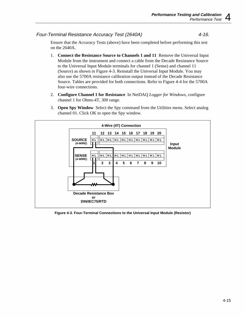
Performance Testing and CalibrationPerformance Test 4
4-15
Four-Terminal Resistance Accuracy Test (2640A) 4-16.
Ensure that the Accuracy Tests (above) have been completed before performing this teston the 2640A.
1. Connect the Resistance Source to Channels 1 and 11 Remove the Universal InputModule from the instrument and connect a cable from the Decade Resistance Sourceto the Universal Input Module terminals for channel 1 (Sense) and channel 11(Source) as shown in Figure 4-3. Reinstall the Universal Input Module. You mayalso use the 5700A resistance calibration output instead of the Decade ResistanceSource. Tables are provided for both connections. Refer to Figure 4-4 for the 5700Afour-wire connections.
2. Configure Channel 1 for Resistance In NetDAQ Logger for Windows, configurechannel 1 for Ohms-4T, 300 range.
3. Open Spy Window Select the Spy command from the Utilities menu. Select analogchannel 01. Click OK to open the Spy window.
1211 13 14 15 16 17 18 19 20
21 3 4 5 6 7 8 9 10
SOURCE(4-WIRE)
SENSE(4-WIRE)
H L H L H L H L H L H L H L H L H L H L
H L H L H L H L H L H L H L H L H L H L
4-Wire (4T) Connection
Decade Resistance Boxor
DIN/IEC75/RTD
InputModule
Figure 4-3. Four-Terminal Connections to the Universal Input Module (Resistor)
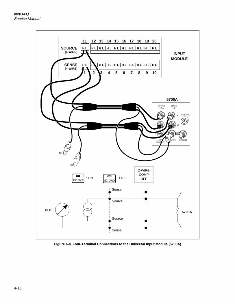
NetDAQService Manual
4-16
1211 13 14 15 16 17 18 19 20
21 3 4 5 6 7 8 9 10
SOURCE(4-WIRE)
SENSE(4-WIRE)
H L H L H L H L H L H L H L H L H L
H L H L H L H L H L H L H L H L H L
INPUTMODULE
HI HI
LO LO
HI
SENSEV
AUXCURRENT
GUARD GROUND
WIDEBAND
5700A
NC
NC
OUTPUTV AΩ Ω
H L
H L
5700AUUT
Sense
Sense
Source
Source
EX GRD: OFF
2-WIRECOMPOFFEX SNS
: ON
Figure 4-4. Four-Terminal Connections to the Universal Input Module (5700A)
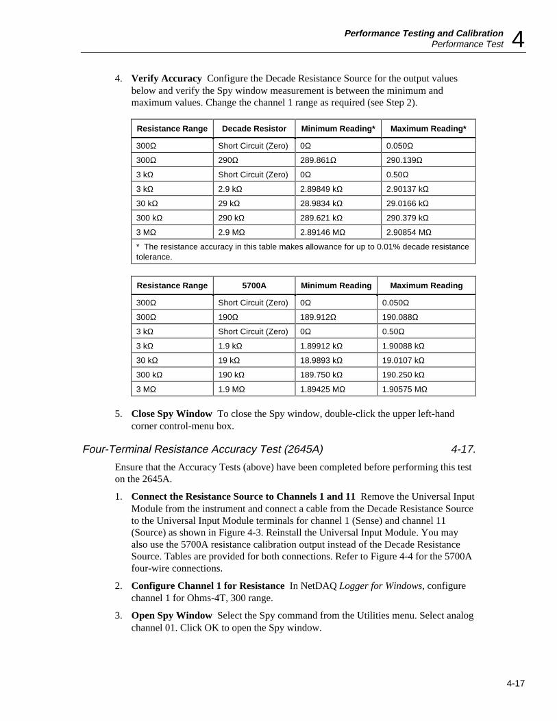
Performance Testing and CalibrationPerformance Test 4
4-17
4. Verify Accuracy Configure the Decade Resistance Source for the output valuesbelow and verify the Spy window measurement is between the minimum andmaximum values. Change the channel 1 range as required (see Step 2).
Resistance Range Decade Resistor Minimum Reading* Maximum Reading*
300Ω Short Circuit (Zero) 0Ω 0.050Ω
300Ω 290Ω 289.861Ω 290.139Ω
3 kΩ Short Circuit (Zero) 0Ω 0.50Ω
3 kΩ 2.9 kΩ 2.89849 kΩ 2.90137 kΩ
30 kΩ 29 kΩ 28.9834 kΩ 29.0166 kΩ
300 kΩ 290 kΩ 289.621 kΩ 290.379 kΩ
3 MΩ 2.9 MΩ 2.89146 MΩ 2.90854 MΩ
* The resistance accuracy in this table makes allowance for up to 0.01% decade resistancetolerance.
Resistance Range 5700A Minimum Reading Maximum Reading
300Ω Short Circuit (Zero) 0Ω 0.050Ω
300Ω 190Ω 189.912Ω 190.088Ω
3 kΩ Short Circuit (Zero) 0Ω 0.50Ω
3 kΩ 1.9 kΩ 1.89912 kΩ 1.90088 kΩ
30 kΩ 19 kΩ 18.9893 kΩ 19.0107 kΩ
300 kΩ 190 kΩ 189.750 kΩ 190.250 kΩ
3 MΩ 1.9 MΩ 1.89425 MΩ 1.90575 MΩ
5. Close Spy Window To close the Spy window, double-click the upper left-handcorner control-menu box.
Four-Terminal Resistance Accuracy Test (2645A) 4-17.
Ensure that the Accuracy Tests (above) have been completed before performing this teston the 2645A.
1. Connect the Resistance Source to Channels 1 and 11 Remove the Universal InputModule from the instrument and connect a cable from the Decade Resistance Sourceto the Universal Input Module terminals for channel 1 (Sense) and channel 11(Source) as shown in Figure 4-3. Reinstall the Universal Input Module. You mayalso use the 5700A resistance calibration output instead of the Decade ResistanceSource. Tables are provided for both connections. Refer to Figure 4-4 for the 5700Afour-wire connections.
2. Configure Channel 1 for Resistance In NetDAQ Logger for Windows, configurechannel 1 for Ohms-4T, 300 range.
3. Open Spy Window Select the Spy command from the Utilities menu. Select analogchannel 01. Click OK to open the Spy window.
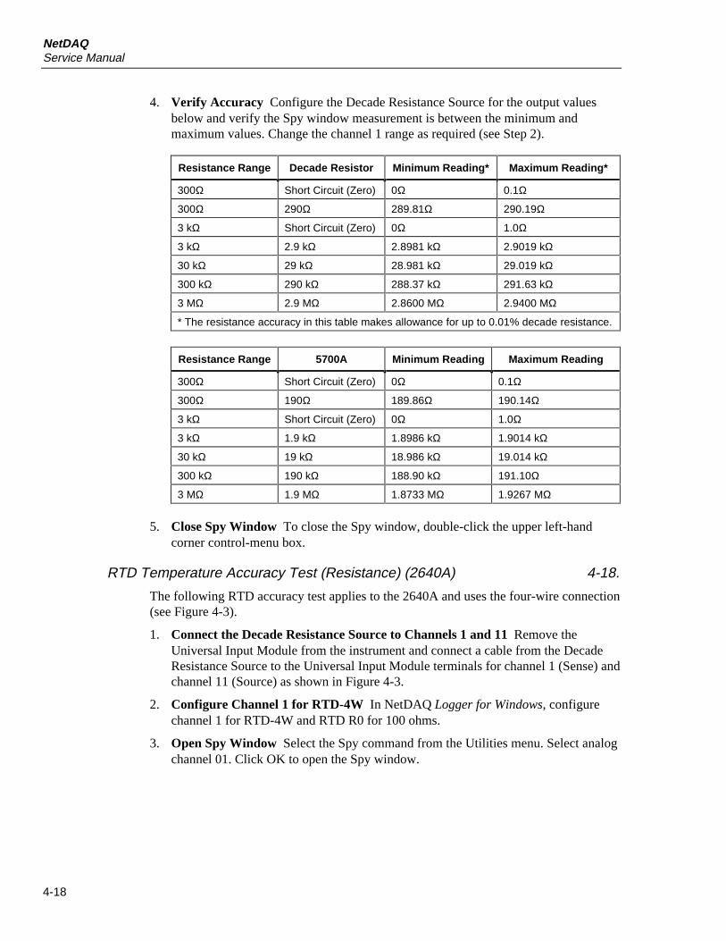
NetDAQService Manual
4-18
4. Verify Accuracy Configure the Decade Resistance Source for the output valuesbelow and verify the Spy window measurement is between the minimum andmaximum values. Change the channel 1 range as required (see Step 2).
Resistance Range Decade Resistor Minimum Reading* Maximum Reading*
300Ω Short Circuit (Zero) 0Ω 0.1Ω
300Ω 290Ω 289.81Ω 290.19Ω
3 kΩ Short Circuit (Zero) 0Ω 1.0Ω
3 kΩ 2.9 kΩ 2.8981 kΩ 2.9019 kΩ
30 kΩ 29 kΩ 28.981 kΩ 29.019 kΩ
300 kΩ 290 kΩ 288.37 kΩ 291.63 kΩ
3 MΩ 2.9 MΩ 2.8600 MΩ 2.9400 MΩ
* The resistance accuracy in this table makes allowance for up to 0.01% decade resistance.
Resistance Range 5700A Minimum Reading Maximum Reading
300Ω Short Circuit (Zero) 0Ω 0.1Ω
300Ω 190Ω 189.86Ω 190.14Ω
3 kΩ Short Circuit (Zero) 0Ω 1.0Ω
3 kΩ 1.9 kΩ 1.8986 kΩ 1.9014 kΩ
30 kΩ 19 kΩ 18.986 kΩ 19.014 kΩ
300 kΩ 190 kΩ 188.90 kΩ 191.10Ω
3 MΩ 1.9 MΩ 1.8733 MΩ 1.9267 MΩ
5. Close Spy Window To close the Spy window, double-click the upper left-handcorner control-menu box.
RTD Temperature Accuracy Test (Resistance) (2640A) 4-18.
The following RTD accuracy test applies to the 2640A and uses the four-wire connection(see Figure 4-3).
1. Connect the Decade Resistance Source to Channels 1 and 11 Remove theUniversal Input Module from the instrument and connect a cable from the DecadeResistance Source to the Universal Input Module terminals for channel 1 (Sense) andchannel 11 (Source) as shown in Figure 4-3.
2. Configure Channel 1 for RTD-4W In NetDAQ Logger for Windows, configurechannel 1 for RTD-4W and RTD R0 for 100 ohms.
3. Open Spy Window Select the Spy command from the Utilities menu. Select analogchannel 01. Click OK to open the Spy window.
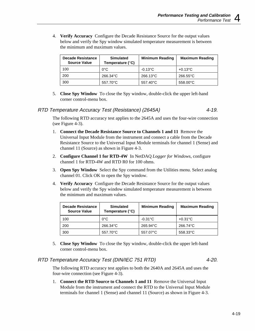
Performance Testing and CalibrationPerformance Test 4
4-19
4. Verify Accuracy Configure the Decade Resistance Source for the output valuesbelow and verify the Spy window simulated temperature measurement is betweenthe minimum and maximum values.
Decade ResistanceSource Value
SimulatedTemperature (°C)
Minimum Reading Maximum Reading
100 0°C -0.13°C +0.13°C
200 266.34°C 266.13°C 266.55°C
300 557.70°C 557.40°C 558.00°C
5. Close Spy Window To close the Spy window, double-click the upper left-handcorner control-menu box.
RTD Temperature Accuracy Test (Resistance) (2645A) 4-19.
The following RTD accuracy test applies to the 2645A and uses the four-wire connection(see Figure 4-3).
1. Connect the Decade Resistance Source to Channels 1 and 11 Remove theUniversal Input Module from the instrument and connect a cable from the DecadeResistance Source to the Universal Input Module terminals for channel 1 (Sense) andchannel 11 (Source) as shown in Figure 4-3.
2. Configure Channel 1 for RTD-4W In NetDAQ Logger for Windows, configurechannel 1 for RTD-4W and RTD R0 for 100 ohms.
3. Open Spy Window Select the Spy command from the Utilities menu. Select analogchannel 01. Click OK to open the Spy window.
4. Verify Accuracy Configure the Decade Resistance Source for the output valuesbelow and verify the Spy window simulated temperature measurement is betweenthe minimum and maximum values.
Decade ResistanceSource Value
SimulatedTemperature (°C)
Minimum Reading Maximum Reading
100 0°C -0.31°C +0.31°C
200 266.34°C 265.94°C 266.74°C
300 557.70°C 557.07°C 558.33°C
5. Close Spy Window To close the Spy window, double-click the upper left-handcorner control-menu box.
RTD Temperature Accuracy Test (DIN/IEC 751 RTD) 4-20.
The following RTD accuracy test applies to both the 2640A and 2645A and uses thefour-wire connection (see Figure 4-3).
1. Connect the RTD Source to Channels 1 and 11 Remove the Universal InputModule from the instrument and connect the RTD to the Universal Input Moduleterminals for channel 1 (Sense) and channel 11 (Source) as shown in Figure 4-3.
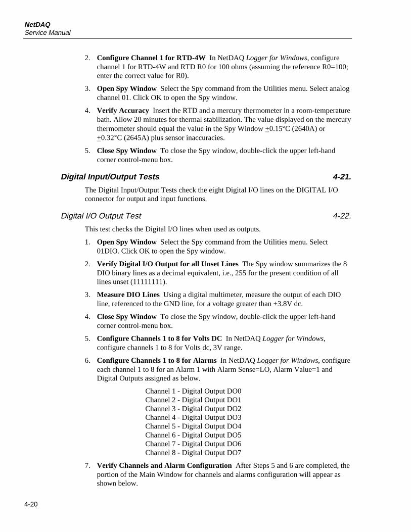
NetDAQService Manual
4-20
2. Configure Channel 1 for RTD-4W In NetDAQ Logger for Windows, configurechannel 1 for RTD-4W and RTD R0 for 100 ohms (assuming the reference R0=100;enter the correct value for R0).
3. Open Spy Window Select the Spy command from the Utilities menu. Select analogchannel 01. Click OK to open the Spy window.
4. Verify Accuracy Insert the RTD and a mercury thermometer in a room-temperaturebath. Allow 20 minutes for thermal stabilization. The value displayed on the mercurythermometer should equal the value in the Spy Window +0.15°C (2640A) or+0.32°C (2645A) plus sensor inaccuracies.
5. Close Spy Window To close the Spy window, double-click the upper left-handcorner control-menu box.
Digital Input/Output Tests 4-21.
The Digital Input/Output Tests check the eight Digital I/O lines on the DIGITAL I/Oconnector for output and input functions.
Digital I/O Output Test 4-22.
This test checks the Digital I/O lines when used as outputs.
1. Open Spy Window Select the Spy command from the Utilities menu. Select01DIO. Click OK to open the Spy window.
2. Verify Digital I/O Output for all Unset Lines The Spy window summarizes the 8DIO binary lines as a decimal equivalent, i.e., 255 for the present condition of alllines unset (11111111).
3. Measure DIO Lines Using a digital multimeter, measure the output of each DIOline, referenced to the GND line, for a voltage greater than +3.8V dc.
4. Close Spy Window To close the Spy window, double-click the upper left-handcorner control-menu box.
5. Configure Channels 1 to 8 for Volts DC In NetDAQ Logger for Windows,configure channels 1 to 8 for Volts dc, 3V range.
6. Configure Channels 1 to 8 for Alarms In NetDAQ Logger for Windows, configureeach channel 1 to 8 for an Alarm 1 with Alarm Sense=LO, Alarm Value=1 andDigital Outputs assigned as below.
Channel 1 - Digital Output DO0Channel 2 - Digital Output DO1Channel 3 - Digital Output DO2Channel 4 - Digital Output DO3Channel 5 - Digital Output DO4Channel 6 - Digital Output DO5Channel 7 - Digital Output DO6Channel 8 - Digital Output DO7
7. Verify Channels and Alarm Configuration After Steps 5 and 6 are completed, theportion of the Main Window for channels and alarms configuration will appear asshown below.
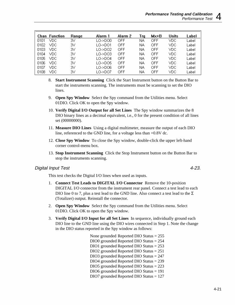
Performance Testing and CalibrationPerformance Test 4
4-21
8. Start Instrument Scanning Click the Start Instrument button on the Button Bar tostart the instruments scanning. The instruments must be scanning to set the DIOlines.
9. Open Spy Window Select the Spy command from the Utilities menu. Select01DIO. Click OK to open the Spy window.
10. Verify Digital I/O Output for all Set Lines The Spy window summarizes the 8DIO binary lines as a decimal equivalent, i.e., 0 for the present condition of all linesset (00000000).
11. Measure DIO Lines Using a digital multimeter, measure the output of each DIOline, referenced to the GND line, for a voltage less than +0.8V dc.
12. Close Spy Window To close the Spy window, double-click the upper left-handcorner control-menu box.
13. Stop Instrument Scanning Click the Stop Instrument button on the Button Bar tostop the instruments scanning.
Digital Input Test 4-23.
This test checks the Digital I/O lines when used as inputs.
1. Connect Test Leads to DIGITAL I/O Connector Remove the 10-positionDIGITAL I/O connector from the instrument rear panel. Connect a test lead to eachDIO line 0 to 7, plus a test lead to the GND line. Also connect a test lead to the Σ(Totalizer) output. Reinstall the connector.
2. Open Spy Window Select the Spy command from the Utilities menu. Select01DIO. Click OK to open the Spy window.
3. Verify Digital I/O Input for all Set Lines In sequence, individually ground eachDIO line to the GND line using the DIO wires connected in Step 1. Note the changein the DIO status reported in the Spy window as follows:
None grounded Reported DIO Status = 255DIO0 grounded Reported DIO Status = 254DIO1 grounded Reported DIO Status = 253DIO2 grounded Reported DIO Status = 251DIO3 grounded Reported DIO Status = 247DIO4 grounded Reported DIO Status = 239DIO5 grounded Reported DIO Status = 223DIO6 grounded Reported DIO Status = 191DIO7 grounded Reported DIO Status = 127
NetDAQService Manual
4-22
4. Close Spy Window To close the Spy window, double-click the upper left-handcorner control-menu box.
Totalizer Tests 4-24.
The Totalizer Tests check the Totalizer feature for counting and sensitivity.
Totalizer Count Test 4-25.
This test checks the ability of the Totalizer feature to count.
1. Configure Channel 1 for Volts DC In NetDAQ Logger for Windows, configurechannel 1 for Volts dc, 3V range.
2. Configure Channel 1 for Alarms In NetDAQ Logger for Windows, configurechannel 1 for an Alarm 1 with Alarm Sense=LO, Alarm Value=1 and DigitalOutput=DO0.
3. Connect Test Leads At the DIGITAL I/O connector, connect the DIO0 test lead tothe Σ (Totalizer) test lead.
4. Start Instrument Scanning Click the Start Instrument button on the Button Bar tostart instrument scanning. Scanning is initiated to enable the return of TOTAL statusto the Spy window.
5. Open Spy Window Select the Spy command from the Utilities menu. Select01TOTAL. Click OK to open the Spy window.
6. Verify Totalizer Count The current totalizer count is 1 since it counted the numberof times channel 1 went into alarm.
7. Close Spy Window To close the Spy window, double-click the upper left-handcorner control-menu box.
8. Increase Totalizer Count Alternately click the Stop Instrument and StartInstrument buttons several times, which advances the Totalizer count as channel 1goes into alarm at the start of each scan.
9. Open Spy Window Select the Spy command from the Utilities menu. Select01TOTAL. Click OK to open the Spy window.
10. Verify Totalizer Count The Spy window summarizes the new Totalizer count andis equal to the number of times the instrument has started and stopped scanning sincethe beginning of this test.
11. Close Spy Window To close the Spy window, double-click the upper left-handcorner control-menu box.
12. Stop Scanning Click the Stop Instrument button on the Button Bar to stopinstrument scanning.
Performance Testing and CalibrationPerformance Test 4
4-23
Totalizer Sensitivity Test 4-26.
This test checks the ability of the Totalizer feature to count voltage transition at aparticular sensitivity level.
1. Connect Test Leads At the DIGITAL I/O connector, connect the Σ (Totalizer) testlead and GND test lead to a signal generator’s output terminals. Adjust the signalgenerator for an output of 1.5V rms sine wave at 10 Hz.
2. Start Instrument Scanning Click the Start Instrument button on the Button Bar tostart instrument scanning. Scanning is initiated to enable the return of TOTAL statusto the Spy window.
3. Open Spy Window Select the Spy command from the Utilities menu. Select01TOTAL. Click OK to open the Spy window.
4. Verify Totalizer Count The Spy window summarizes the Totalizer count. Verifythe totalizer count is advancing at approximately 10 Hz per Spy window update(nominal 1 second intervals).
5. Close Spy Window To close the Spy window, double-click the upper left-handcorner control-menu box.
6. Stop Scanning Click the Stop Instrument button on the Button Bar to stopinstrument scanning.
Master Alarm Output Test 4-27.
This test checks the Master Alarm output for a logic low when a channel is in alarm.
1. Connect Test Leads to ALARM/TRIGGER I/O Connector Remove the8-position ALARM/TRIGGER I/O connector from the instrument rear panel.Connect a test lead to each line, MA (Master Alarm), TO (Trigger Output), TI(Trigger Input), plus a test lead to the GND line. Reinstall the connector.
2. Measure Unset MA Line Using a digital multimeter, measure the output of theunset MA test lead, referenced to the GND test lead, for a voltage greater than +3.8Vdc.
3. Verify Configuration Channel 1 for Volts DC In NetDAQ Logger for Windows,verify channel 1 is configured for Volts dc, 3V range.
4. Verify Configuration Channel 1 for Alarms In NetDAQ Logger for Windows,verify channel 1 is configured for an Alarm 1 with Alarm Sense=LO, AlarmValue=1 and Digital Output=DO0.
5. Start Instrument Scanning Click the Start Instrument button on the Button Bar tostart instrument scanning. Scanning is initiated to enable the Master Alarm output.
6. Measure Set MA Line Using a digital multimeter, measure the output of the setMA test lead, referenced to the GND test lead, for a voltage less than +0.8V dc.
7. Stop Scanning Click the Stop Instrument button on the Button Bar to stopinstrument scanning.
NetDAQService Manual
4-24
Trigger Input Test 4-28.
This test checks the ability of the Trigger Input line to trigger measurement scanning.
1. Configure Trigger Input In NetDAQ Logger for Windows, configure the scanparameters for External Trigger with an Interval 2 of 1 second. Be sure IntervalTrigger is not enabled.
2. Verify Configuration Channel 1 for Volts DC In NetDAQ Logger for Windows,verify channel 1 is configured for Volts dc, 3V range.
3. Start Instrument Scanning Click the Start Instrument button on the Button Bar toenable instrument scanning, although no measurement scanning takes place becausethe external Trigger Input is not set.
4. Open Logging Status Window Select the Show Logging Status command from theOptions menu to display the Logging Status window.
5. Verify Logging Status Note in the Logging Status window that the Retrieved Scanscount is zero and not incrementing.
6. Set Trigger Input While monitoring the Logging Status window, connect the TI(Trigger Input) test lead to the GND test lead. Note in the Logging Status window,the Retrieved Scans count increments at 1-second intervals. Disconnect the TI andGND test lead connection.
7. Stop Scanning Click the Stop Instrument button on the Button Bar to stopinstrument scanning.
Trigger Output Test 4-29.
This test checks the Trigger Output (125µs logic low) that occurs each time theinstrument scans.
1. Configure Interval Trigger In NetDAQ Logger for Windows, configure the scanparameters for Interval Trigger with an Interval 1 of 1 second.
2. Verify Configuration Channel 1 for Volts DC In NetDAQ Logger for Windows,verify channel 1 is configured for Volts dc, 3V range.
3. Measure Unset Trigger Output Line Using a digital multimeter, measure theoutput of the unset TO test lead, referenced to the GND test lead, for a voltagegreater than +3.8V dc.
4. Verify Trigger Output is Enabled In NetDAQ Logger for Windows, click theInstrument Config button on the Button Bar. In the Instrument Configuration dialogbox, verify the Trigger Out box is checked. Click OK to return to the Main Window.
5. Connect Trigger Output Connect the TO test lead on the ALARM/TRIGGER IOconnector to the Σ (Totalizer) test lead on the DIGITAL I/O connector. This allowseach Trigger Output pulse to be counted by the Totalizer.
6. Start Instrument Scanning Click the Start Instrument button on the Button Bar toenable instrument scanning.
7. Open Spy Window Select the Spy command from the Utilities menu. Select01TOTAL. Click OK to open the Spy window.
Performance Testing and CalibrationCalibration 4
4-25
8. Verify Totalizer Count The Spy window summarizes the Totalizer count. Note theTotalizer is incrementing at 1-second intervals as it counts the Trigger Output pulseat the start of each scan.
9. Close Spy Window To close the Spy window, double-click the upper left-handcorner control-menu box.
10. Stop Scanning Click the Stop Instrument button on the Button Bar to stopinstrument scanning.
Calibration 4-30.The instrument features calibration that is completed over the NetDAQ networked dataacquisition unit RS-232 interface, and it is not necessary to open the instrument case.Using known reference sources, closed-case calibration has many advantages. There areno parts to disassemble, no mechanical adjustments to make, and the instrument can becalibrated by an automated instrumentation system. The instrument should normally becalibrated on a regular cycle, typically every 90 days to 1 year. The chosen calibrationcycle depends on the accuracy specification you wish to maintain. The instrument shouldalso be calibrated if it fails the performance test or has undergone repair.
The calibration procedure uses the CAL ENABLE switch under the Calibration Seal onthe instrument front panel. Do not press CAL ENABLE unless you intend to calibratethe instrument. If you have entered calibration and wish to exit, press CAL ENABLEuntil CAL is removed from the primary display, or just turn the instrument power off.
Once the instrument is in calibration mode, closed-case calibration is made for the fourcalibration groups as follows:
• Volts DC• Volts AC• Resistance• Frequency
Once begun, each group must be completed successfully for the results of the calibrationto be made permanent. It is not necessary to perform all calibration groups.
Methods of Calibration 4-31.
There three methods of instrument calibration as follows:
• Automatic using Fluke MET/CAL software MET/CAL is a software packagedeveloped by Fluke that automates the calibration of Fluke instruments and popularinstruments from other selected manufacturers.
• Semiautomatic using NetDAQ Logger for Windows Calibration takes place inconjunction with NetDAQ Logger for Windows, that is, a feature of the software isused to calibrate the instrument. Since calibration is accomplished over an RS-232connection between the instrument RS-232 port and a host computer serial COMport, it is not necessary to have a network connection to accomplish calibration.
• Manual using a terminal and individual commands Calibration takes place usinga host computer in a terminal mode. With this method all commands and responsesare considered individually.
NetDAQService Manual
4-26
All methods use the instrument RS-232 serial interface. Procedures cannot be performedover the network interface or from the instrument front panel.
Preparing for Calibration 4-32.
Regardless of the method you are using for calibration (automatic, semiautomatic, ormanual), the preparation for calibration is identical. Complete the following procedure toprepare for calibration.
1. Connect the instrument RS-232 serial port to a host computer COM serial port asshown in Figure 4-5. You can connect two instruments as shown, although only oneis calibrated at a time. The “RS” cables used are standard null-modem cables(reversed transmit and receive lines) that may be ordered from Fluke.
2. Wire the Universal Input Module so the high and low inputs to channels 1 and 11 areexternally available. In addition, a four-wire short must be applied to channels 2 and12. (See Figure 4-6.) Plug the module into the instrument.
3. Power the instrument and allow at least a 30-minute warmup period. The instrumentmust be stabilized in an environment with an ambient temperature of 22 to 24°C andrelative humidity of less than 70%.
4. Using the buttons at the instrument front panel, set the desired baud rate for theinstrument RS-232 port (see below). This is the only selectable RS-232 parameter.The other instrument RS-232 parameters are fixed: data bits=8; stops bits=1;parity=none; echo=none; flow control=xon/xoff.
COMM Press the COMM key to review the baud rate, or press and hold the COMM keyfor 3 seconds to set the baud rate (the SET annunciator lights).
Press the up/down arrow keys until rS232 is shown in the primary display(comm is displayed in the secondary display).
ENTER Press the ENTER key. bAud is displayed in the secondary display and thecurrent baud rate in the primary display.
Press the up/down arrow keys to select the desired number baud rate:4800, 9600, 19200, or 38400. The factory default value is 9600 baud.
ENTER Press the ENTER key to exit. (Pressing any other function key will cancel setoperations.)
5. Activate the calibration mode at the instrument by pressing and holding theinstrument front panel CAL Enable button for approximately 4 seconds. Release thebutton after instrument beeps and CAL is shown on the primary display.
NOTE
The CAL Enable button is located on the right side of the display beneath acalibration seal. Press this button with a blunt-tipped object. Do not pressCAL ENABLE unless you intend to calibrate the instrument. If you haveactivated Calibration and wish to exit, press CAL ENABLE momentarily asecond time, or turn the instrument off.
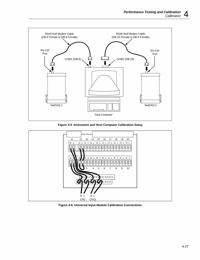
Performance Testing and CalibrationCalibration 4
4-27
Host Computer
NetDAQ 1 NetDAQ 2
RS40 Null Modem Cable(DB-25 Female to DB-9 Female)
RS43 Null Modem Cable(DB-9 Female to DB-9 Female)
RS-232Port
COM2 (DB-25)
RS-232Port
COM1 (DB-9)
Figure 4-5. Instrument and Host Computer Calibration Setup
LHH L H L H L H L H L H L H L H L H L
H L H L H L H L H L H L H L H L H L H L
1
11
2
12
3
13
4
14
5
15
6
16
7
17
8
18
9
19
10
20
H LCH1
H LCH11
Figure 4-6. Universal Input Module Calibration Connections
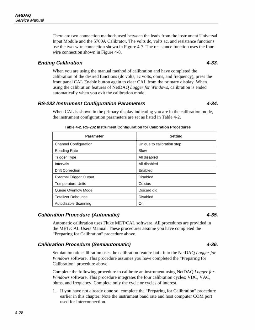
NetDAQService Manual
4-28
There are two connection methods used between the leads from the instrument UniversalInput Module and the 5700A Calibrator. The volts dc, volts ac, and resistance functionsuse the two-wire connection shown in Figure 4-7. The resistance function uses the four-wire connection shown in Figure 4-8.
Ending Calibration 4-33.
When you are using the manual method of calibration and have completed thecalibration of the desired functions (dc volts, ac volts, ohms, and frequency), press thefront panel CAL Enable button again to clear CAL from the primary display. Whenusing the calibration features of NetDAQ Logger for Windows, calibration is endedautomatically when you exit the calibration mode.
RS-232 Instrument Configuration Parameters 4-34.
When CAL is shown in the primary display indicating you are in the calibration mode,the instrument configuration parameters are set as listed in Table 4-2.
Table 4-2. RS-232 Instrument Configuration for Calibration Procedures
Parameter Setting
Channel Configuration Unique to calibration step
Reading Rate Slow
Trigger Type All disabled
Intervals All disabled
Drift Correction Enabled
External Trigger Output Disabled
Temperature Units Celsius
Queue Overflow Mode Discard old
Totalizer Debounce Disabled
Autodisable Scanning On
Calibration Procedure (Automatic) 4-35.
Automatic calibration uses Fluke MET/CAL software. All procedures are provided inthe MET/CAL Users Manual. These procedures assume you have completed the“Preparing for Calibration” procedure above.
Calibration Procedure (Semiautomatic) 4-36.
Semiautomatic calibration uses the calibration feature built into the NetDAQ Logger forWindows software. This procedure assumes you have completed the “Preparing forCalibration” procedure above.
Complete the following procedure to calibrate an instrument using NetDAQ Logger forWindows software. This procedure integrates the four calibration cycles: VDC, VAC,ohms, and frequency. Complete only the cycle or cycles of interest.
1. If you have not already done so, complete the “Preparing for Calibration” procedureearlier in this chapter. Note the instrument baud rate and host computer COM portused for interconnection.
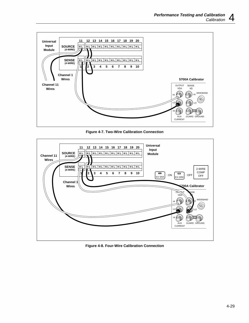
Performance Testing and CalibrationCalibration 4
4-29
1211 13 14 15 16 17 18 19 20
21 3 4 5 6 7 8 9 10
SOURCE(4-WIRE)
SENSE(4-WIRE)
H L H L H L H L H L H L H L H L
H L H L H L H L H L H L H L H L
UniversalInput
Module
HI HI
LO LO
HI
OUTPUTV A
SENSEV
AUXCURRENT
GUARD GROUND
WIDEBAND
Ω Ω
5700A CalibratorChannel 1
Wires
Channel 11Wires
H L
H L H L
H L
Figure 4-7. Two-Wire Calibration Connection
1211 13 14 15 16 17 18 19 20
21 3 4 5 6 7 8 9 10
SOURCE(4-WIRE)
SENSE(4-WIRE)
H L H L H L H L H L H L H L H L
H L H L H L H L H L H L H L H L
UniversalInput
Module
HI HI
LO LO
HI
OUTPUTV A
SENSEV
AUXCURRENT
GUARD GROUND
WIDEBAND
Ω Ω
5700A CalibratorChannel 1
Wires
Channel 11Wires
EX GRD: OFF
2-WIRECOMPOFFEX SNS
: ON
H L
H L H L
H L
Figure 4-8. Four-Wire Calibration Connection
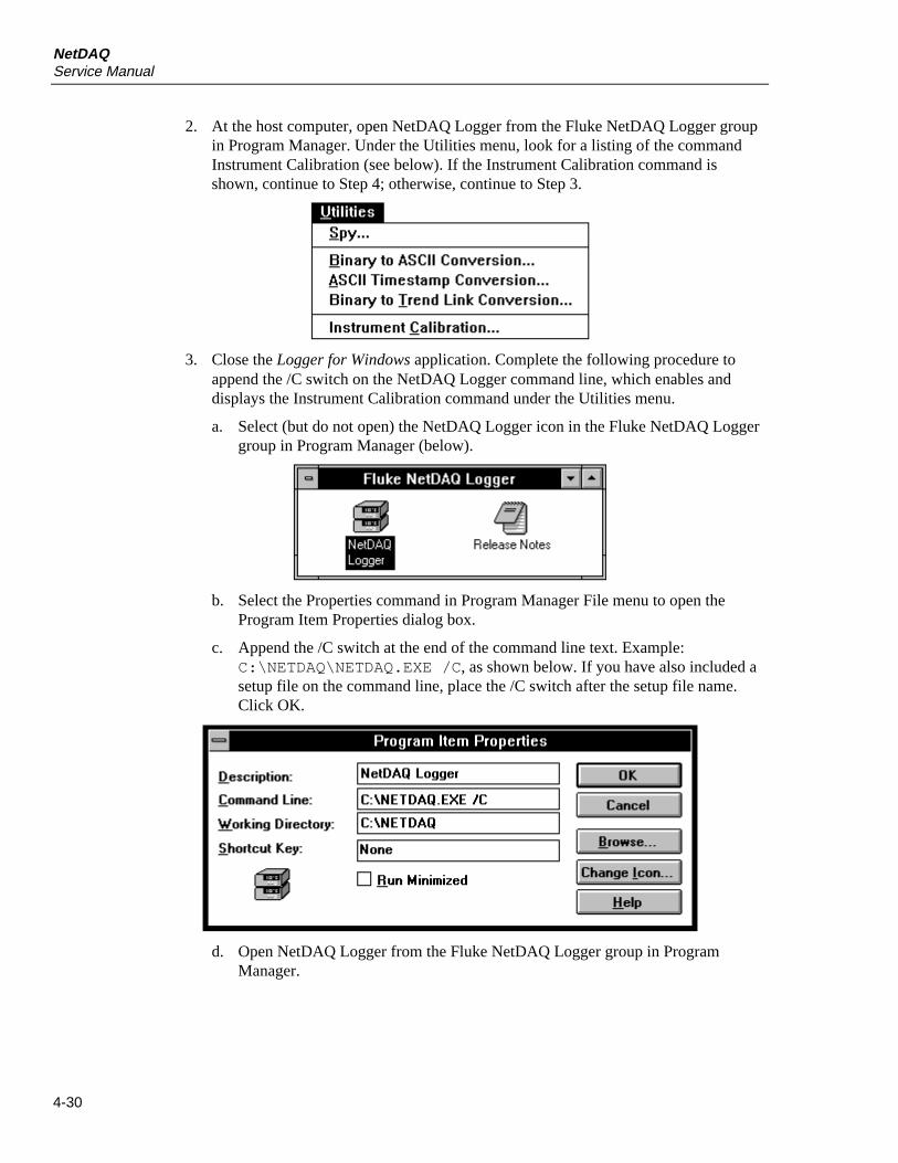
NetDAQService Manual
4-30
2. At the host computer, open NetDAQ Logger from the Fluke NetDAQ Logger groupin Program Manager. Under the Utilities menu, look for a listing of the commandInstrument Calibration (see below). If the Instrument Calibration command isshown, continue to Step 4; otherwise, continue to Step 3.
3. Close the Logger for Windows application. Complete the following procedure toappend the /C switch on the NetDAQ Logger command line, which enables anddisplays the Instrument Calibration command under the Utilities menu.
a. Select (but do not open) the NetDAQ Logger icon in the Fluke NetDAQ Loggergroup in Program Manager (below).
b. Select the Properties command in Program Manager File menu to open theProgram Item Properties dialog box.
c. Append the /C switch at the end of the command line text. Example:C:\NETDAQ\NETDAQ.EXE /C, as shown below. If you have also included asetup file on the command line, place the /C switch after the setup file name.Click OK.
d. Open NetDAQ Logger from the Fluke NetDAQ Logger group in ProgramManager.

Performance Testing and CalibrationCalibration 4
4-31
4. Select the Instrument Calibration command from the Utilities menu, opening theInstrument Calibration dialog box (below).
5. Select the COM port and baud rate noted in Step 1. The instrument default baud rateis 9600 baud.
VDC Calibration Procedure 4-37.
This procedure uses the calibration feature of NetDAQ Logger for Windows. Completethe “Calibration Procedure (Semiautomatic)” before using this procedure.
1. Click the Volts DC button in the Instrument Calibration dialog box, opening the firstCalibration Steps - Volts DC dialog box (below).
If you get an error message, check the RS-232 parameter settings, and cabling, andmake sure no other application such as terminal or internal modem is using theselected COM port. The error “Calibration Mode not enabled” means you have notpressed the CAL enable button at the instrument front panel.
2. Connect the 5700A Calibrator as shown in Figure 4-7 and source an output of 0.09Vdc. Click the Perform Calibration Step button to calibrate the selected value. Afterthe calibration step completes, the next calibration appears in the Actual box.
3. In a similar manner, source the 5700A Calibrator for the values 0.3V, .75V, 3V andso forth until the Done button is no longer dimmed.
NetDAQService Manual
4-32
4. Click the Done button to exit the volts dc calibration cycle.
5. If this completes your calibration requirements, click the Close button in theInstrument Calibration dialog box to return to the NetDAQ Logger for WindowsMain Window. Otherwise, continue to the next calibration function.
VAC Calibration Procedure 4-38.
This procedure uses the calibration feature of NetDAQ Logger for Windows. Completethe “Calibration Procedure (Semiautomatic)” before using this procedure.
1. Click the Volts AC button in the Instrument Calibration dialog box, opening the firstCalibration Steps - Volts AC dialog box (below).
If you get an error message, check the RS-232 parameter settings, and cabling, andmake sure no other application such as terminal or internal modem is using theselected COM port. The error “Calibration Mode not enabled” means you have notpressed the CAL enable button at the instrument front panel.
2. Connect the 5700A Calibrator as shown in Figure 4-7 and source an output of 0.03Vac at a frequency of 1 kHz. Click the Perform Calibration Step button to calibrate theselected value. After the calibration step completes, the next calibration appears inthe Actual box.
3. In a similar manner, source the 5700A Calibrator for the values 0.3V, 0.3V, 3V, 3V(values repeat) and so forth until the Done button is no longer dimmed.
4. Click the Done button to exit the volts ac calibration cycle.
5. If this completes your calibration requirements, click the Close button in theInstrument Calibration dialog box to return to the NetDAQ Logger for WindowsMain Window. Otherwise, continue to the next calibration function.
Performance Testing and CalibrationCalibration 4
4-33
Resistance Calibration Procedure 4-39.
This procedure uses the calibration feature of NetDAQ Logger for Windows. Completethe “Calibration Procedure (Semiautomatic)” before using this procedure.
1. Click the Resistance button in the Instrument Calibration dialog box, opening thefirst Calibration Steps - Resistance dialog box (below).
If you get an error message, check the RS-232 parameter settings, and cabling, andmake sure no other application such as terminal or internal modem is using theselected COM port. The error “Calibration Mode not enabled” means you have notpressed the CAL enable button at the instrument front panel.
2. Connect the 5700A Calibrator as shown in Figure 4-8 and source an output of 190ohms. Note that this must be a four-wire connection. Also verify the calibratoroutput is set up for a four-wire source. Click the Perform Calibration Step button tocalibrate the selected value. After the calibration step completes, the next calibrationappears in the Actual box.
3. In a similar manner, source the 5700A Calibrator for the values 1.9k, 19k, 190kohms and so forth until the Done button is no longer dimmed.
4. Click the Done button to exit the resistance calibration cycle.
5. If this completes your calibration requirements, click the Close button in theInstrument Calibration dialog box to return to the NetDAQ Logger for WindowsMain Window. Otherwise, continue to the next calibration function.
NetDAQService Manual
4-34
Frequency Calibration Procedure 4-40.
This procedure uses the calibration feature of NetDAQ Logger for Windows. Completethe “Calibration Procedure (Semiautomatic)” before using this procedure.
1. Click the Frequency button in the Instrument Calibration dialog box, opening theCalibration Steps - Frequency dialog box (below).
If you get an error message, check the RS-232 parameter settings, and cabling, andmake sure no other application such as terminal or internal modem is using theselected COM port. The error “Calibration Mode not enabled” means you have notpressed the CAL enable button at the instrument front panel.
2. Connect the 5700A Calibrator as shown in Figure 4-7 and source an output of 3V acat 10 kHz. Click the Perform Calibration Step button. There is only a single value.
3. Click the Done button to exit the frequency cycle.
Calibration Procedure (Manual) 4-41.
Manual calibration uses a calibration command set operated over an ASCII terminal or acomputer running a terminal emulation program. The following procedure assumes youwill be using the Windows Terminal feature of your host computer. If you are using adifferent terminal, adapt this procedure to suit.
Complete the following procedure to prepare the Windows Terminal feature.
1. Complete the “Preparing for Calibration” procedure earlier in this chapter. Note theinstrument baud rate and host computer COM port that you selected for use.
2. Open Windows to the Program Manager screen on your host computer.
3. Open Terminal (below) from the Accessory group of Program Manager.
Performance Testing and CalibrationCalibration 4
4-35
4. Select the Communications command from the Setting menu. Enter the sameRS-232 baud rate and host computer COM noted in Step 1. The other parameters areselected as shown below. Click OK.
5. Select the Terminal Preferences command from the Settings menu. Check the boxesLocal Echo and Outbound (see below). Click OK.
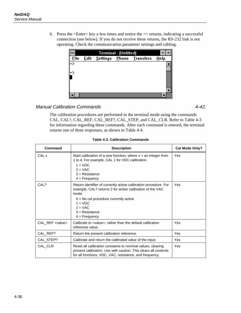
NetDAQService Manual
4-36
6. Press the <Enter> key a few times and notice the => returns, indicating a successfulconnection (see below). If you do not receive these returns, the RS-232 link is notoperating. Check the communication parameter settings and cabling.
Manual Calibration Commands 4-42.
The calibration procedures are performed in the terminal mode using the commandsCAL, CAL?, CAL_REF, CAL_REF?, CAL_STEP, and CAL_CLR. Refer to Table 4-3for information regarding these commands. After each command is entered, the terminalreturns one of three responses, as shown in Table 4-4.
Table 4-3. Calibration Commands
Command Description Cal Mode Only?
CAL x Start calibration of a new function, where x = an integer from1 to 4. For example, CAL 1 for VDC calibration.
1 = VDC2 = VAC3 = Resistance4 = Frequency
Yes
CAL? Return identifier of currently active calibration procedure. Forexample, CAL? returns 2 for active calibration of the VACmode.
0 = No cal procedure currently active1 = VDC2 = VAC3 = Resistance4 = Frequency
Yes
CAL_REF <value> Calibrate to <value>, rather than the default calibrationreference value.
Yes
CAL_REF? Return the present calibration reference. Yes
CAL_STEP? Calibrate and return the calibrated value of the input. Yes
CAL_CLR Reset all calibration constants to nominal values, clearingpresent calibration. Use with caution. This clears all contentsfor all functions, VDC, VAC, resistance, and frequency.
Yes
Performance Testing and CalibrationCalibration 4
4-37
Table 4-4. Manual Calibration Command Responses
Response Description
=> indicates the command was executed correctly.
!> indicates that a device-dependent error was generated and the calibration step could not beexecuted. Verify that the input to NetDAQ channel 1 is the correct value and polarity, isconnected correctly, and the 5700A is in the Operate mode.
?> indicates the command was entered with incorrect syntax, for example, misspelling thecommand. Reenter the command using the correct syntax.
Manual VDC Calibration Procedure 4-43.
The VDC calibration procedure calculates gain and offset calibration constants for all ofthe VDC ranges. The 750 mV range is not user accessible, but is used to measure thereference junction voltage and must be calibrated.
Complete the following procedure to manually calibrate the VDC function.
1. If you have not already done so, complete the procedure “Preparing for Calibration”earlier in this chapter.
2. Connect the instrument and 5700A Calibrator as shown in Figure 4-7.
3. Complete the sequence of manual steps shown in Table 4-5. Measuring channel 1provides the full scale reading, and measuring the short on channel 2 determines thezero offset error. Both readings are accomplished automatically with theCAL_STEP? command.
Table 4-5. Manual VDC Calibration
Command Response Action
CAL 1 => Puts NetDAQ in VDC calibration.
CAL_REF? +90.0000E-3 5700A - Source 90 mV dc.
CAL_STEP? +90.0000E-3 NetDAQ computes the calibration constant and returnsthe calibrated reading. Allow several seconds.
CAL_REF? +300.000E-3 5700A - Source 300 mV dc.
CAL_STEP? +300.000E-3 NetDAQ computes the calibration constant and returnsthe calibrated reading. Allow several seconds.
CAL_REF? +750.000E-3 5700A - Source 750 mV dc.
CAL_STEP? +750.000E-3 NetDAQ computes the calibration constant and returnsthe calibrated reading. Allow several seconds.
CAL_REF? +3.00000E+0 5700A - Source 3V dc.
CAL_STEP? +3.00000E+0 NetDAQ computes the calibration constant and returnsthe calibrated reading. Allow several seconds.
CAL_REF? +30.0000E+0 5700A - Source 30V dc.
CAL_STEP? +30.0000E+0 NetDAQ computes the calibration constant and returnsthe calibrated reading. Allow several seconds.
CAL_REF? +300.000E+0 (2640A)+50.0000E+0 (2645A)
5700A - Source +300V dc (2640A).5700A - Source +50V dc (2645A).
CAL_STEP? +300.000E+0 (2640A)+50.0000E+0 (2645A)
NetDAQ computes the calibration constant and returnsthe calibrated reading. Allow several seconds.
NetDAQService Manual
4-38
4. Resolve any calibration problems based on the following:
• An execution error !> is returned by the CAL_STEP? command if the full scalemeasurement is off by more than 5% from the target or if the zero measurementis off by more than 1% of full scale from the target. When an error is detected,the cal constant is not updated, and the procedure remains at the same step.
• When CAL_STEP? reports an execution error !> due to an out-of-rangemeasurement, it returns the raw measured reading to give you an indication ofwhat was measured. When CAL_STEP? completes successfully, it returns thereference value.
• If CAL_STEP? returns an execution error !> while measuring the short circuiton channel 2, the procedure freezes at the internal step that measures the short.This way, you can send a CAL_REF? command and it will return 0 V, indicatingthat the problem was probably caused by a misapplied short on channel 2.
• A device-dependent error is returned by the CAL_STEP? command if an internalerror such as a measurement timeout is detected. When an error is detected, thecal constant is not updated, and the procedure remains at the same step.
• An execution error !> is returned by the CAL_REF command if the specifiedreference is less than 33% of full scale or greater than 100% of full scale.
Manual VAC Calibration Procedure 4-44.
The VAC calibration procedure calculates gain and offset calibration constants for all ofthe VAC ranges.
Complete the following procedure to manually calibrate the VAC function.
1. If you have not already done so, complete the procedure “Preparing for Calibration”earlier in this chapter.
2. Connect the instrument and 5700A Calibrator as shown in Figure 4-7.
3. Complete the sequence of manual steps shown in Table 4-6. Measurements are madeon channel 1 for each VAC range: one at 10% of full scale and one at 100% of fullscale. All AC voltages must be applied at 1 kHz. The VAC gain and offsetcalibration constants for each range are determined from the two measurements.
4. Resolve any calibration problems based on the following:
• An execution error !> is returned by the CAL_STEP? command if the full-scalemeasurement is off by more than 10% from the target or if the low-scalemeasurement is off by more than 1% of full scale (10% from the target). Whenan error is detected, the cal constant is not updated, and the procedure remains atthe same step.
• A device-dependent error is returned by the CAL_STEP? command if an internalerror such as a measurement timeout is detected. When an error is detected, thecal constant is not updated, and the procedure remains at the same step.
• An execution error !> is returned by the CAL_REF command for the full scalemeasurement if the specified reference is less than 33% of full scale or greaterthan 100% of full scale for any range. An execution error !> is returned by theCAL_REF command for the low scale measurement if the specified reference isless than 10% of full scale or greater than 30% of full scale for any range.
Performance Testing and CalibrationCalibration 4
4-39
Table 4-6. Manual VAC Calibration
Command Response Action
CAL 2 => Puts NetDAQ in VAC calibration.
CAL_REF? 30.0000E-3 5700A - Source 30 mV ac @ 1 kHz
CAL_STEP? 30.0000E-3 NetDAQ computes the calibration constant and returnsthe calibrated reading. Allow several seconds.
CAL_REF? 300.000E-3 5700A - Source 300 mV ac @ 1 kHz
CAL_STEP? 300.000E-3 NetDAQ computes the calibration constant and returnsthe calibrated reading. Allow several seconds.
CAL_REF? 300.000E-3 5700A - Source 300 mV ac @ 1 kHz
CAL_STEP? 300.000E-3 NetDAQ computes the calibration constant and returnsthe calibrated reading. Allow several seconds.
CAL_REF? 3.00000E+0 5700A - Source 3V ac @ 1 kHz
CAL_STEP? 3.00000E+0 NetDAQ computes the calibration constant and returnsthe calibrated reading. Allow several seconds.
CAL_REF? 3.0000E+0 5700A - Source 3V ac @ 1 kHz
CAL_STEP? 3.0000E+0 NetDAQ computes the calibration constant and returnsthe calibrated reading. Allow several seconds.
CAL_REF? 30.0000E+0 5700A - Source 30V ac @ 1 kHz
CAL_STEP? 30.0000E+0 NetDAQ computes the calibration constant and returnsthe calibrated reading. Allow several seconds.
[2640A only for remainder of steps]
CAL_REF? 30.0000E+0 5700A - Source 30V ac @ 1 kHz
CAL_STEP? 30.0000E+0 NetDAQ computes the calibration constant and returnsthe calibrated reading. Allow several seconds.
CAL_REF? 300.0000E+0 5700A - Source 300V ac @ 1 kHz
CAL_STEP? 300.0000E+0 NetDAQ computes the calibration constant and returnsthe calibrated reading. Allow several seconds.
Manual Resistance Calibration Procedure 4-45.
The resistance calibration procedure calculates gain and offset calibration constants forall of the four-wire ohms ranges. The same calibration constants are used for thecorresponding two-wire ohms ranges.
Complete the following procedure to manually calibrate the ohms function.
1. If you have not already done so, complete the procedure “Preparing for Calibration”earlier in this chapter.
2. Connect the instrument and 5700A Calibrator as shown in Figure 4-8.
3. Complete the sequence of manual steps shown in Table 4-7. The default values werechosen assuming that a Fluke 5700A will be used to supply the reference resistors.For each range, channels 1 and 2 are configured to four-wire ohms and ameasurement is made for each channel. Making a four-wire ohms measurement onchannel 1 provides the full scale reading and measuring the four-wire short onchannels 2 and 12 determines the zero offset error. The four-wire ohms gain andoffset calibration constants are determined from these two measurements.
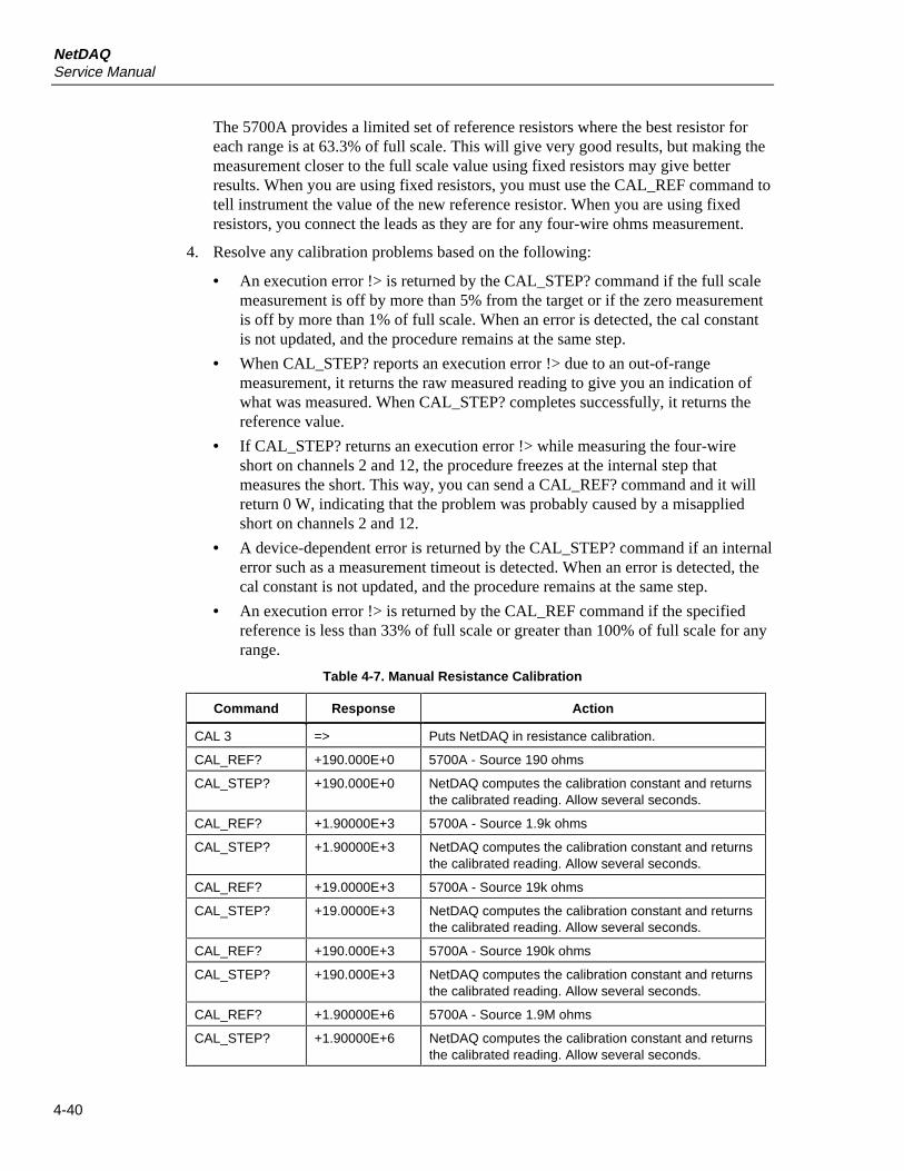
NetDAQService Manual
4-40
The 5700A provides a limited set of reference resistors where the best resistor foreach range is at 63.3% of full scale. This will give very good results, but making themeasurement closer to the full scale value using fixed resistors may give betterresults. When you are using fixed resistors, you must use the CAL_REF command totell instrument the value of the new reference resistor. When you are using fixedresistors, you connect the leads as they are for any four-wire ohms measurement.
4. Resolve any calibration problems based on the following:
• An execution error !> is returned by the CAL_STEP? command if the full scalemeasurement is off by more than 5% from the target or if the zero measurementis off by more than 1% of full scale. When an error is detected, the cal constantis not updated, and the procedure remains at the same step.
• When CAL_STEP? reports an execution error !> due to an out-of-rangemeasurement, it returns the raw measured reading to give you an indication ofwhat was measured. When CAL_STEP? completes successfully, it returns thereference value.
• If CAL_STEP? returns an execution error !> while measuring the four-wireshort on channels 2 and 12, the procedure freezes at the internal step thatmeasures the short. This way, you can send a CAL_REF? command and it willreturn 0 W, indicating that the problem was probably caused by a misappliedshort on channels 2 and 12.
• A device-dependent error is returned by the CAL_STEP? command if an internalerror such as a measurement timeout is detected. When an error is detected, thecal constant is not updated, and the procedure remains at the same step.
• An execution error !> is returned by the CAL_REF command if the specifiedreference is less than 33% of full scale or greater than 100% of full scale for anyrange.
Table 4-7. Manual Resistance Calibration
Command Response Action
CAL 3 => Puts NetDAQ in resistance calibration.
CAL_REF? +190.000E+0 5700A - Source 190 ohms
CAL_STEP? +190.000E+0 NetDAQ computes the calibration constant and returnsthe calibrated reading. Allow several seconds.
CAL_REF? +1.90000E+3 5700A - Source 1.9k ohms
CAL_STEP? +1.90000E+3 NetDAQ computes the calibration constant and returnsthe calibrated reading. Allow several seconds.
CAL_REF? +19.0000E+3 5700A - Source 19k ohms
CAL_STEP? +19.0000E+3 NetDAQ computes the calibration constant and returnsthe calibrated reading. Allow several seconds.
CAL_REF? +190.000E+3 5700A - Source 190k ohms
CAL_STEP? +190.000E+3 NetDAQ computes the calibration constant and returnsthe calibrated reading. Allow several seconds.
CAL_REF? +1.90000E+6 5700A - Source 1.9M ohms
CAL_STEP? +1.90000E+6 NetDAQ computes the calibration constant and returnsthe calibrated reading. Allow several seconds.
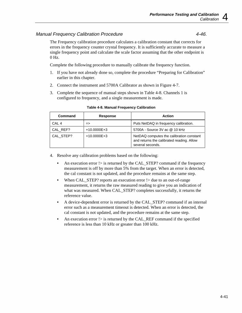
Performance Testing and CalibrationCalibration 4
4-41
Manual Frequency Calibration Procedure 4-46.
The Frequency calibration procedure calculates a calibration constant that corrects forerrors in the frequency counter crystal frequency. It is sufficiently accurate to measure asingle frequency point and calculate the scale factor assuming that the other endpoint is0 Hz.
Complete the following procedure to manually calibrate the frequency function.
1. If you have not already done so, complete the procedure “Preparing for Calibration”earlier in this chapter.
2. Connect the instrument and 5700A Calibrator as shown in Figure 4-7.
3. Complete the sequence of manual steps shown in Table 4-8. Channels 1 isconfigured to frequency, and a single measurement is made.
Table 4-8. Manual Frequency Calibration
Command Response Action
CAL 4 => Puts NetDAQ in frequency calibration.
CAL_REF? +10.0000E+3 5700A - Source 3V ac @ 10 kHz
CAL_STEP? +10.0000E+3 NetDAQ computes the calibration constantand returns the calibrated reading. Allowseveral seconds.
4. Resolve any calibration problems based on the following:
• An execution error !> is returned by the CAL_STEP? command if the frequencymeasurement is off by more than 5% from the target. When an error is detected,the cal constant is not updated, and the procedure remains at the same step.
• When CAL_STEP? reports an execution error !> due to an out-of-rangemeasurement, it returns the raw measured reading to give you an indication ofwhat was measured. When CAL_STEP? completes successfully, it returns thereference value.
• A device-dependent error is returned by the CAL_STEP? command if an internalerror such as a measurement timeout is detected. When an error is detected, thecal constant is not updated, and the procedure remains at the same step.
• An execution error !> is returned by the CAL_REF command if the specifiedreference is less than 10 kHz or greater than 100 kHz.

NetDAQService Manual
4-42
5-1
Chapter 5Diagnostic Testing and Troubleshooting
Title Page
5-1. Introduction ............................................................................................ 5-35-2. Servicing Surface-Mount Assemblies.................................................... 5-35-3. Error Detection....................................................................................... 5-45-4. FLASH ROM Parameter Defaults ..................................................... 5-55-5. Background Testing ........................................................................... 5-55-6. Internal Software Errors..................................................................... 5-65-7. Retrieving Error Codes using RS-232 ............................................... 5-65-8. Retrieving Error Codes using the Network........................................ 5-65-9. Selecting the Diagnostic Tools............................................................... 5-65-10. Diagnostic Tool dio............................................................................ 5-75-11. Diagnostic Tool idS ........................................................................... 5-75-12. Diagnostic Tool conF......................................................................... 5-85-13. Diagnostic Display Test ..................................................................... 5-95-14. COMM Parameter Reset.................................................................... 5-95-15. Using the RS-232 Interface .................................................................... 5-95-16. Command Processing......................................................................... 5-105-17. Instrument Configuration................................................................... 5-115-18. Command Set..................................................................................... 5-125-19. Troubleshooting the Instrument ............................................................. 5-195-20. General Troubleshooting ................................................................... 5-195-21. A1 Main PCA Troubleshooting ......................................................... 5-275-22. Troubleshooting the A1 Main PCA Digital Kernel....................... 5-275-23. Troubleshooting the RS-232 Interface .......................................... 5-285-24. Troubleshooting the Ethernet Interface ......................................... 5-285-25. Troubleshooting the Digital I/O Lines and Trigger Out Lines...... 5-285-26. Troubleshooting the Totalizer and Trigger In Lines ..................... 5-285-27. Troubleshooting the Power Supply ............................................... 5-295-28. A2 Display PCA Troubleshooting ..................................................... 5-295-29. Variations in the Display ............................................................... 5-31
NetDAQService Manual
5-2
5-30. A3 A/D Converter PCA Troubleshooting.......................................... 5-315-31. A3 Kernel....................................................................................... 5-325-32. Break/Reset Circuit........................................................................ 5-325-33. Out of Tolerance Readings ............................................................ 5-325-34. Troubleshooting Relay Problems .................................................. 5-335-35. A4 Analog Input PCA Troubleshooting ............................................ 5-335-36. Troubleshooting Calibration Failures .................................................... 5-345-37. Retrieving Calibration Constants....................................................... 5-345-38. Loading Embedded Instrument Firmware ............................................. 5-365-39. Firmware Diskette.............................................................................. 5-365-40. Loading the Main Firmware .............................................................. 5-375-41. Loading the A/D Firmware................................................................ 5-38
Diagnostic Testing and TroubleshootingIntroduction 5
5-3
Introduction 5-1.The instrument provides error code information and semi-modular design to aid introubleshooting. This section explains the error codes and describes procedures neededto isolate a problem to a specific functional area. Finally, troubleshooting hints for eachfunctional area are presented.
But first, if the instrument fails, check the line voltage fuse and replace as needed. If theproblem persists, verify that you are operating the instrument correctly by reviewing theoperating instructions found in the instrument Users Manual.
WARNING
Opening the case may expose hazardous voltages. Alwaysdisconnect the power cord and measuring inputs beforeopening the case. And remember that repairs or servicingshould be performed only by qualified personnel.
Required calibration equipment is listed in Chapter 4 of this manual. Signal namesfollowed by a ’*’ are active (asserted) low. Signal names not so marked are active high.
Servicing Surface-Mount Assemblies 5-2.The instrument incorporates Surface-Mount Technology (SMT) for printed circuitassemblies (pca’s). Surface-mount components are much smaller than their predecessors,with leads soldered directly to the surface of a circuit board; no plated through-holes areused. Unique servicing, troubleshooting, and repair techniques are required to supportthis technology. The information offered in the following paragraphs serves only as anintroduction to SMT. It is not recommended that repair be attempted based only on theinformation presented here. Refer to the Fluke "Surface-Mount Device Soldering Kit"for a complete demonstration and discussion of these techniques. (In the USA, call 1-800-526-4731 to order.)
Since sockets are seldom used with SMT, "shotgun" troubleshooting cannot be used; afault should be isolated to the component level before a part is replaced. Surface-mountassemblies are probed from the component side. The probes should make contact onlywith the pads in front of the component leads. With the close spacing involved, ordinarytest probes can easily short two adjacent pins on an SMT IC.
This Service Manual is a vital source for component locations and values. With limitedspace on the circuit board, chip component locations are seldom labeled. Figuresprovided in Chapter 6 of this manual provide this information. Also, remember that chipcomponents are not individually labeled; keep any new or removed component in alabeled package.
Surface-mount components are removed and replaced by reflowing all the solderconnections at the same time. Special considerations are required.
• The solder tool uses regulated hot air to melt the solder; there is no direct contactbetween the tool and the component.
• Surface-mount assemblies require rework with wire solder rather than with solderpaste. A 0.025-inch diameter wire solder composed of 63% tin and 37% lead isrecommended. A 60/40 solder is also acceptable.
NetDAQService Manual
5-4
• A good connection with SMT requires only enough solder to make a positivemetallic contact. Too much solder causes bridging, while too little solder can causeweak or open solder joints. With SMT, the anchoring effect of the through-holes ismissing; solder provides the only means of mechanical fastening. Therefore, the pcamust be especially clean to ensure a strong connection. An oxidized pca pad causesthe solder to wick up the component lead, leaving little solder on the pad itself.
Refer to the Fluke "Surface-Mount Device Soldering Kit" for a complete discussion ofthese techniques.
Error Detection 5-3.At power-up, the instrument software performs self-tests. If any errors in instrumentoperation are detected, they are reported on the instrument front panel with Error in theprimary display and a decimal error code number in the secondary display. If there ismore than one error, they are displayed sequentially. Selftest errors can be retrieved fromRS-232 commands and the network.
A selftest includes a test of the following items:
• FLASH ROM parameters, communication parameters and calibration constants.
• RAM Instrument and channel configuration plus RAM images of FLASH ROMparameters.
• Ethernet Ethernet chip and static Ethernet RAM.
• Display Display processor and display board
• Inguard Specific tests for ROM checksum, RAM, A/D converter, zero offset test,reference balance test, ohms overload test, and otc.
A summary of the possible error codes are shown in Table 5-1, including the front panelerror code (in decimal) and the corresponding network and RS-232 error code (inhexadecimal). The faults that might cause each error are described in “Troubleshootingthe Instrument” later in this chapter.
Table 5-1. Selftest Error Codes
Front PanelError Codes
RS-232 QueryError Codes
Error Codes inhexadecimal Error Code Description
(None) 0 0x00000000 No selftest error.
1 1 0x00000001 Bad boot software image in FLASH ROM.
2 2 0x00000002 Bad main software image in FLASH ROM.
3 4 0x00000004 RAM test failure.
4 8 0x00000008 Display test failure.
5 16 0x00000010 Display not responding.
6 32 0x00000020 Calibration constants corrupt.
7 64 0x00000040 Inguard not responding.
8 128 0x00000080 Inguard A/D failure.
9 256 0x00000100 Inguard zero offsets test failed.
Diagnostic Testing and TroubleshootingError Detection 5
5-5
Table 5-1. Selftest Error Codes (cont)
Front PanelError Codes
RS-232 QueryError Codes
Error Codes inhexadecimal Error Code Description
10 512 0x00000200 Inguard reference balance test failed.
11 1024 0x00000400 Inguard overload detection failed.
12 2048 0x00000800 Inguard open thermocouple detect failed.
13 4096 0x00001000 Communication parameters corrupt.
14 8192 0x00002000 Ethernet address parameter corrupt.
15 16384 0x00004000 RAM constants corrupt.
16 32768 0x00008000 Ethernet chip or RAM failure.
FLASH ROM Parameter Defaults 5-4.
The FLASH ROM (U21 Main Board) parameters are reset to defaults following the firstpower-on and following power-cycles after any FLASH ROM parameters are discoveredto be corrupt. These defaults are listed in Table 5-2.
Table 5-2. FLASH ROM Parameter Defaults
Parameter Default
Ethernet Address ff:ff:ff:ff:ff:ff
Calibration Constants All gains are set to 1.0; all offsets are set to 0.0
IP Address 255.255.255.255
Port Number 4369
RS-232 Baud Rate 19200
BCN 1
Line Frequency 60 Hz
Network Type 0 (isolated network)
Background Testing 5-5.
Background testing is performed to ensure that communication, configuration, andcalibration constants do not become corrupt over time. Every 10 seconds, one of theparameter sets is verified (verifying all parameter sets at once is too CPU intensive). Thefollowing parameter sets are checked:
• FLASH ROM communication parameters
• FLASH ROM calibration constants
• FLASH ROM Ethernet address
• RAM instrument and channel configuration
• RAM pre-computed range scaling and calibration constants used in evaluation
• RAM copy of calibration constants
• RAM copy of Ethernet address
NetDAQService Manual
5-6
When a parameter set is discovered to be corrupt, the background testing task records theerror in the error/status register, and performs any corrective action required. The errorsand actions performed on the errors are listed in the below Table 5-3.
Table 5-3. Corrective Action for Background Error Checking
Error Action
FLASH ROM communication parameters corrupt. Reset to defaults on next power-up.
FLASH ROM calibration constants corrupt. Reset to defaults on next power-up.
FLASH ROM Ethernet address corrupt. Reset to defaults on next power-up.Network interfaces will not activate.
Any RAM constants corrupt. None.
Internal Software Errors 5-6.
Internal software errors are any software conditions which should never occur. Internalerrors are recorded in an internal store, and can be retrieved with the User NetworkInterface request NETCMD_IERROR. In addition, the front panel will display the errornumber, and the error/status bit EST_INTERNAL_ERROR will be set.
Retrieving Error Codes using RS-232 5-7.
You can retrieve error codes from the instrument using the instrument rear-panel RS-232port and an ASCII terminal, or PC running ASCII terminal emulation.
Complete the following procedure to retrieve error codes from the instrument using anRS-232 connection.
1. Connect the instrument to a PC COM port and setup the RS-232 parameters andconnection as described in the procedure “Calibration Procedure (Manual)” inChapter 4.
2. Enter the command *TST? to invoke the instrument selftest routine and return theresult, or just SELFTEST? for the results of the most recent self test. If you use*TST?, allow several seconds for the tests to complete. The *TST? test does notinclude the RAM test because this test cannot be performed when the instrument isoperating.
3. Observe the returned number after the selftest routine. Refer to Table 5-1 for ananalysis of the return. For example, a return of 64 is the same as error code 7 on thefront panel display.
Retrieving Error Codes using the Network 5-8.
A selftest can be performed from the User Network Interface with theNETCMD_RUN_SELFTEST network command.
Selecting the Diagnostic Tools 5-9.This section describes the instrument diagnostic tool menu and other diagnostic features.The diagnostic tool menu is hidden from the user. There are three separate diagnostictools that can be selected from the menu, each of which is described below.
Diagnostic Testing and TroubleshootingSelecting the Diagnostic Tools 5
5-7
Complete the following procedure to select the diagnostic tools.
1. Power the instrument and allow it to complete the normal power-on sequence.
2. Press and hold the DIO key for 3 seconds until “tool” appears in the secondarydisplay.
3. Use the up/down arrow keys to sequence you through the three diagnostic selections:
• dio (used to set any of the instrument rear-panel dio7 to dio0 digital i/o lines)
• idS (used to display the various firmware versions active within the instrument)
• conF (used to configure the reading rate, and channel functions and ranges)
4. Select the desired diagnostic tool using the up/down arrow keys; then press theENTER key.
Other diagnostic tools include the display test and COMM parameter reset.
Diagnostic Tool dio 5-10.
The dio diagnostic tool allows you to change the status of any eight dio lines dio7 to dio0located on the instrument rear-panel DIGITAL I/O connector.
Complete the following procedure to change the status of any dio line.
1. Select the dio diagnostic tool using the procedure “Selecting the Diagnostic ToolMenu.”
2. Use the left/right arrows to select the desired dio line dio7 to dio0. The format isnnnn-nnnn, representing dio lines dio7 to dio0, respectively. The secondary displayshows the selected line, for example, dio:7.
3. Use the up/down arrow keys to select the desired dio line status, 0 or 1.
4. In a similar manner, select the desired dio status for each line dio7 to dio0; then
press the ENTER key to return to the diagnostic tool menu.
5. Select another diagnostic tool using the up/down arrow key, or exit by pressing theDIO key. The dio lines remain set after exiting this procedure.
Diagnostic Tool idS 5-11.
The idS diagnostic tool allows you to view the firmware versions installed in yourinstrument.
Complete the following procedure to view the firmware versions in your instrument.
1. Select the idS diagnostic tool using the procedure “Selecting the Diagnostic ToolMenu.”
2. With inStr shown in the secondary display, and the instrument model number shownin the primary display, press the up/down arrow keys to sequence through thefirmware selections shown in Table 5-4.
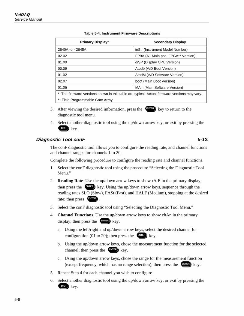
NetDAQService Manual
5-8
Table 5-4. Instrument Firmware Descriptions
Primary Display* Secondary Display
2640A -or- 2645A inStr (Instrument Model Number)
02.02 FP9A (A1 Main pca, FPGA** Version)
01.00 diSP (Display CPU Version)
00.09 Atodb (A/D Boot Version)
01.02 AtodM (A/D Software Version)
02.07 boot (Main Boot Version)
01.05 MAin (Main Software Version)
* The firmware versions shown in this table are typical. Actual firmware versions may vary.
** Field Programmable Gate Array
3. After viewing the desired information, press the ENTER key to return to thediagnostic tool menu.
4. Select another diagnostic tool using the up/down arrow key, or exit by pressing theDIO key.
Diagnostic Tool conF 5-12.
The conF diagnostic tool allows you to configure the reading rate, and channel functionsand channel ranges for channels 1 to 20.
Complete the following procedure to configure the reading rate and channel functions.
1. Select the conF diagnostic tool using the procedure “Selecting the Diagnostic ToolMenu.”
2. Reading Rate Use the up/down arrow keys to show rAtE in the primary display;
then press the ENTER key. Using the up/down arrow keys, sequence through thereading rates SLO (Slow), FASt (Fast), and HALF (Medium), stopping at the desired
rate; then press ENTER .
3. Select the conF diagnostic tool using “Selecting the Diagnostic Tool Menu.”
4. Channel Functions Use the up/down arrow keys to show chAn in the primary
display; then press the ENTER key.
a. Using the left/right and up/down arrow keys, select the desired channel for
configuration (01 to 20); then press the ENTER key.
b. Using the up/down arrow keys, chose the measurement function for the selected
channel; then press the ENTER key.
c. Using the up/down arrow keys, chose the range for the measurement function
(except frequency, which has no range selection); then press the ENTER key.
5. Repeat Step 4 for each channel you wish to configure.
6. Select another diagnostic tool using the up/down arrow key, or exit by pressing theDIO key.
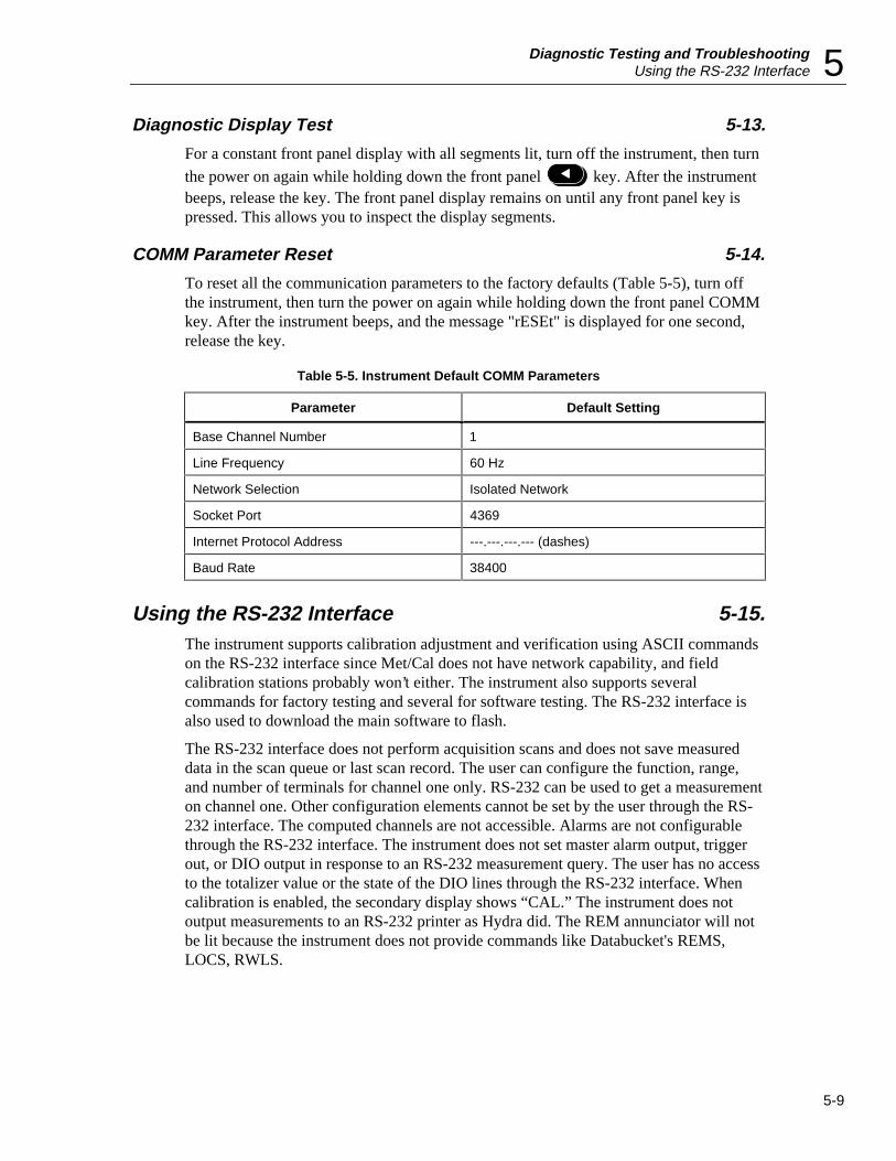
Diagnostic Testing and TroubleshootingUsing the RS-232 Interface 5
5-9
Diagnostic Display Test 5-13.
For a constant front panel display with all segments lit, turn off the instrument, then turn
the power on again while holding down the front panel key. After the instrumentbeeps, release the key. The front panel display remains on until any front panel key ispressed. This allows you to inspect the display segments.
COMM Parameter Reset 5-14.
To reset all the communication parameters to the factory defaults (Table 5-5), turn offthe instrument, then turn the power on again while holding down the front panel COMMkey. After the instrument beeps, and the message "rESEt" is displayed for one second,release the key.
Table 5-5. Instrument Default COMM Parameters
Parameter Default Setting
Base Channel Number 1
Line Frequency 60 Hz
Network Selection Isolated Network
Socket Port 4369
Internet Protocol Address ---.---.---.--- (dashes)
Baud Rate 38400
Using the RS-232 Interface 5-15.The instrument supports calibration adjustment and verification using ASCII commandson the RS-232 interface since Met/Cal does not have network capability, and fieldcalibration stations probably won’t either. The instrument also supports severalcommands for factory testing and several for software testing. The RS-232 interface isalso used to download the main software to flash.
The RS-232 interface does not perform acquisition scans and does not save measureddata in the scan queue or last scan record. The user can configure the function, range,and number of terminals for channel one only. RS-232 can be used to get a measurementon channel one. Other configuration elements cannot be set by the user through the RS-232 interface. The computed channels are not accessible. Alarms are not configurablethrough the RS-232 interface. The instrument does not set master alarm output, triggerout, or DIO output in response to an RS-232 measurement query. The user has no accessto the totalizer value or the state of the DIO lines through the RS-232 interface. Whencalibration is enabled, the secondary display shows “CAL.” The instrument does notoutput measurements to an RS-232 printer as Hydra did. The REM annunciator will notbe lit because the instrument does not provide commands like Databucket's REMS,LOCS, RWLS.
NetDAQService Manual
5-10
Command Processing 5-16.
The instrument RS-232 interface processes input and output in a manner similar toHydra. The instrument receives a command or query from the host. The instrumentreturns a response to a valid query. The instrument always returns a prompt afterprocessing an input line (the prompt follows the response in the case of a query).
An input line to the instrument consists of one or more semicolon-separated commandsfollowed by an input terminator. The instrument will accept CR/LF or LF as the inputterminator. The instrument reads input into a 350-byte input queue until it finds the inputterminator. The instrument does not echo input. While processing the queued input, theinstrument parses and processes each command in sequence. Therefore, earliercommands can execute even if a later command contains a syntax error.
The prompts have the following meanings:
=> No error. Command was parsed and executed with no errors.
?> Command error. The command contained a syntax error. For example, the commandname or an argument contained a type; the command was not a legal command; anargument was of the wrong type; too many or too few arguments were supplied. Sinceparity is always set to none, parity errors cause garbage in the input buffer, and this willgenerate a syntax error (at best).
!> Execution or device-dependent error. An execution error occurs when the commandwas recognized to be an instrument command but was not legal given the current state ofthe instrument, or had an inappropriate parameter value. A device-dependent erroroccurs when an instrument-specific limitation is exceeded (such as input queue size), orwhen the instrument tries to execute the command but it fails (for example, due to a badCRC).
If a command cannot be recognized (i.e., syntax error), the instrument returns the ?>error prompt and does not do any more processing on that command or the remainingcontents of the input queue. If a query had already been processed on that line, itsresponse would be sent before the prompt.
If the input queue size is exceeded, the instrument throws away all further input until itreceives a terminator, and generates a device-dependent error. None of the commands inthe queue are executed. The instrument returns the !> prompt when it encounters theinput terminator.
If the instrument receives an input line before its last prompt has been read out of itsoutput queue, the instrument will generate an execution error, return the !> error promptinstead of whatever prompt it had planned to return, and ignore the second input line.
If an input line contains more than one query command, the responses will be returned inone response line separated by semicolons.
When sending a response or prompt, the instrument appends an output terminator whichis the CR/LF character. The instrument output can be held off with XON/XOFF.
The string formats and general syntax rules are the same as Hydra’s.
The following settings are fixed: eight data bits, no parity, no echo, XON/XOFF flowcontrol, no CTS flow control. The user can set the baud rate to 4800, 9600, 19200, or38400.
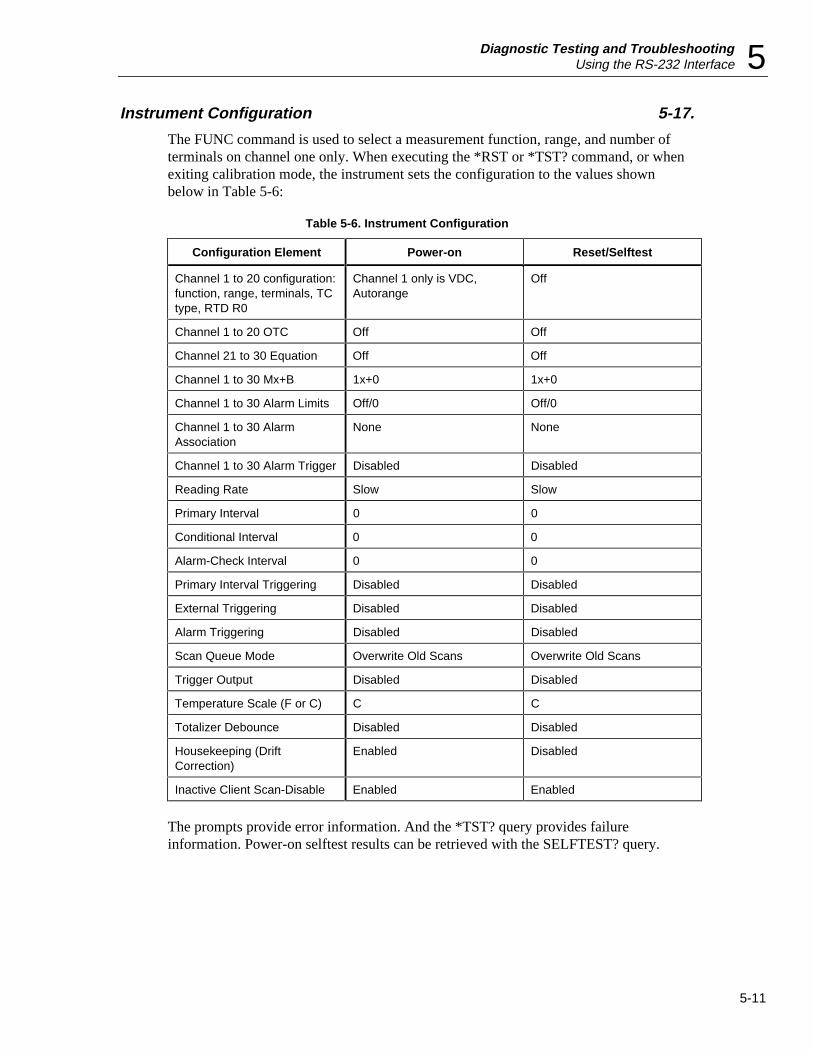
Diagnostic Testing and TroubleshootingUsing the RS-232 Interface 5
5-11
Instrument Configuration 5-17.
The FUNC command is used to select a measurement function, range, and number ofterminals on channel one only. When executing the *RST or *TST? command, or whenexiting calibration mode, the instrument sets the configuration to the values shownbelow in Table 5-6:
Table 5-6. Instrument Configuration
Configuration Element Power-on Reset/Selftest
Channel 1 to 20 configuration:function, range, terminals, TCtype, RTD R0
Channel 1 only is VDC,Autorange
Off
Channel 1 to 20 OTC Off Off
Channel 21 to 30 Equation Off Off
Channel 1 to 30 Mx+B 1x+0 1x+0
Channel 1 to 30 Alarm Limits Off/0 Off/0
Channel 1 to 30 AlarmAssociation
None None
Channel 1 to 30 Alarm Trigger Disabled Disabled
Reading Rate Slow Slow
Primary Interval 0 0
Conditional Interval 0 0
Alarm-Check Interval 0 0
Primary Interval Triggering Disabled Disabled
External Triggering Disabled Disabled
Alarm Triggering Disabled Disabled
Scan Queue Mode Overwrite Old Scans Overwrite Old Scans
Trigger Output Disabled Disabled
Temperature Scale (F or C) C C
Totalizer Debounce Disabled Disabled
Housekeeping (DriftCorrection)
Enabled Disabled
Inactive Client Scan-Disable Enabled Enabled
The prompts provide error information. And the *TST? query provides failureinformation. Power-on selftest results can be retrieved with the SELFTEST? query.
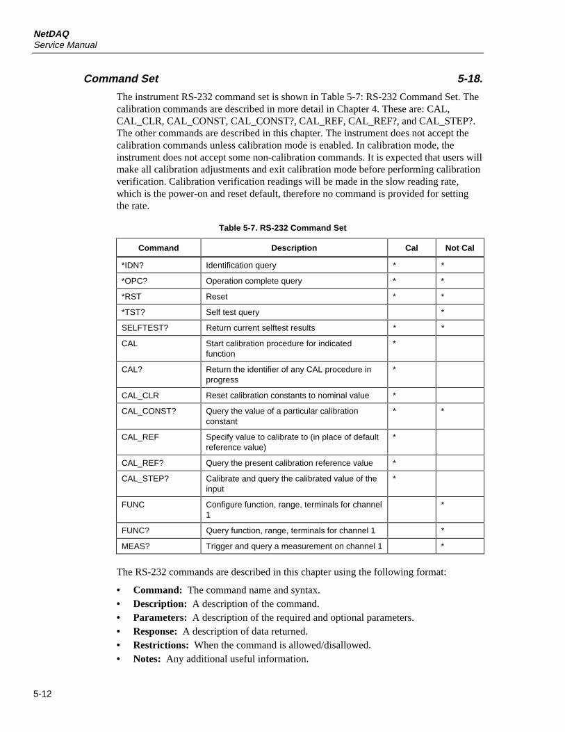
NetDAQService Manual
5-12
Command Set 5-18.
The instrument RS-232 command set is shown in Table 5-7: RS-232 Command Set. Thecalibration commands are described in more detail in Chapter 4. These are: CAL,CAL_CLR, CAL_CONST, CAL_CONST?, CAL_REF, CAL_REF?, and CAL_STEP?.The other commands are described in this chapter. The instrument does not accept thecalibration commands unless calibration mode is enabled. In calibration mode, theinstrument does not accept some non-calibration commands. It is expected that users willmake all calibration adjustments and exit calibration mode before performing calibrationverification. Calibration verification readings will be made in the slow reading rate,which is the power-on and reset default, therefore no command is provided for settingthe rate.
Table 5-7. RS-232 Command Set
Command Description Cal Not Cal
*IDN? Identification query * *
*OPC? Operation complete query * *
*RST Reset * *
*TST? Self test query *
SELFTEST? Return current selftest results * *
CAL Start calibration procedure for indicatedfunction
*
CAL? Return the identifier of any CAL procedure inprogress
*
CAL_CLR Reset calibration constants to nominal value *
CAL_CONST? Query the value of a particular calibrationconstant
* *
CAL_REF Specify value to calibrate to (in place of defaultreference value)
*
CAL_REF? Query the present calibration reference value *
CAL_STEP? Calibrate and query the calibrated value of theinput
*
FUNC Configure function, range, terminals for channel1
*
FUNC? Query function, range, terminals for channel 1 *
MEAS? Trigger and query a measurement on channel 1 *
The RS-232 commands are described in this chapter using the following format:
• Command: The command name and syntax.• Description: A description of the command.• Parameters: A description of the required and optional parameters.• Response: A description of data returned.• Restrictions: When the command is allowed/disallowed.• Notes: Any additional useful information.
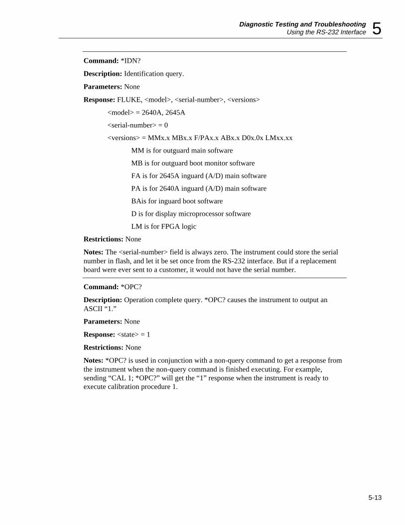
Diagnostic Testing and TroubleshootingUsing the RS-232 Interface 5
5-13
Command: *IDN?
Description: Identification query.
Parameters: None
Response: FLUKE, <model>, <serial-number>, <versions>
<model> = 2640A, 2645A
<serial-number> = 0
<versions> = MMx.x MBx.x F/PAx.x ABx.x D0x.0x LMxx.xx
MM is for outguard main software
MB is for outguard boot monitor software
FA is for 2645A inguard (A/D) main software
PA is for 2640A inguard (A/D) main software
BAis for inguard boot software
D is for display microprocessor software
LM is for FPGA logic
Restrictions: None
Notes: The <serial-number> field is always zero. The instrument could store the serialnumber in flash, and let it be set once from the RS-232 interface. But if a replacementboard were ever sent to a customer, it would not have the serial number.
Command: *OPC?
Description: Operation complete query. *OPC? causes the instrument to output anASCII “1.”
Parameters: None
Response: <state> = 1
Restrictions: None
Notes: *OPC? is used in conjunction with a non-query command to get a response fromthe instrument when the non-query command is finished executing. For example,sending “CAL 1; *OPC?” will get the “1” response when the instrument is ready toexecute calibration procedure 1.
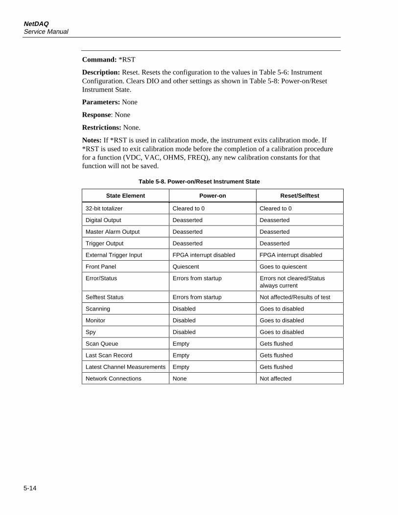
NetDAQService Manual
5-14
Command: *RST
Description: Reset. Resets the configuration to the values in Table 5-6: InstrumentConfiguration. Clears DIO and other settings as shown in Table 5-8: Power-on/ResetInstrument State.
Parameters: None
Response: None
Restrictions: None.
Notes: If *RST is used in calibration mode, the instrument exits calibration mode. If*RST is used to exit calibration mode before the completion of a calibration procedurefor a function (VDC, VAC, OHMS, FREQ), any new calibration constants for thatfunction will not be saved.
Table 5-8. Power-on/Reset Instrument State
State Element Power-on Reset/Selftest
32-bit totalizer Cleared to 0 Cleared to 0
Digital Output Deasserted Deasserted
Master Alarm Output Deasserted Deasserted
Trigger Output Deasserted Deasserted
External Trigger Input FPGA interrupt disabled FPGA interrupt disabled
Front Panel Quiescent Goes to quiescent
Error/Status Errors from startup Errors not cleared/Statusalways current
Selftest Status Errors from startup Not affected/Results of test
Scanning Disabled Goes to disabled
Monitor Disabled Goes to disabled
Spy Disabled Goes to disabled
Scan Queue Empty Gets flushed
Last Scan Record Empty Gets flushed
Latest Channel Measurements Empty Gets flushed
Network Connections None Not affected
Diagnostic Testing and TroubleshootingUsing the RS-232 Interface 5
5-15
Command: *TST?
Description: Selftest query. Initiates asynchronous selftest and then returns the selftestresults. This command resets the instrument configuration and state the same as *RST.
Parameters: None
Response: <selftest-result> = an integer which binary-encodes the selftest results asshown in Table 5-1: Selftest Error Codes. Multiple selftest errors are indicated by theselftest codes or’d together.
Restrictions: Not allowed in calibration mode.
Command: SELFTEST?
Description: Selftest results query. Returns the selftest results from the last selftestperformed. This command can be used to retrieve the power-on selftest results.
Parameters: None
Response: <selftest-result> = an integer which binary-encodes the selftest results asshown in Table 5-1. Multiple selftest errors are indicated by the selftest codes or’dtogether.
Restrictions: Not allowed in calibration mode.
Command: CAL
Description: Initiate calibration procedure for the specified measurement function.
Parameters: <procedure>
<procedure> =
1 = VDC
2 = VAC
3 = Ohms
4 = Frequency
Response: None
Restrictions: Only allowed in Calibration Mode
Notes: If executed during a calibration procedure, it aborts the current procedure andbegins another.
This command returns an execution error if not in the Calibration Mode.
This command returns a device dependent error if an internal error such as a guardcrossing error is detected while attempting to determine the instrument type.
This command returns a device dependent error if it is unable to set the default calconfiguration. This could happen if scanning was enabled via the network interface afterthe cal procedure was initiated.
NetDAQService Manual
5-16
Command: CAL?
Description: Return the procedure identifier of any calibration procedure in progress
Parameters: none
Response: <procedure>
where <procedure> =
0 = No calibration procedure currently active
1 = VDC
2 = VAC
3 = Ohms
4 = Frequency
Restrictions: Only allowed in Calibration Mode
Notes: This command returns an execution error if not in the Calibration Mode.
NetDAQ Logger for Windows uses this command to determine when a calibrationprocedure has completed.
Command: CAL_REF
Description: Specify value to calibrate to in place of default reference
Parameters: <new calibration reference value>
<new calibration reference value> = floating point reference value
Response: None
Restrictions: Calibration mode only
Notes: This command returns an execution error if the specified calibration reference isinvalid. The allowable limits for each reference are specified for each procedure inChapter 4, “Performance Testing and Calibration.” This command returns an executionerror if no cal procedure is active.
Command: CAL_REF?
Description: Query the present calibration reference value
Parameters: None
Response: <reference value>
<reference value> = floating point number
Restrictions: Calibration mode only
Notes: This command returns an execution error if no cal procedure is active.
Diagnostic Testing and TroubleshootingUsing the RS-232 Interface 5
5-17
Command: CAL_STEP?
Description: Calibrate and query the calibrated value of the input
Parameters: None
Response: <calibrated value>
<calibrated value> = floating point number
Restrictions: Calibration mode only
Notes: This command returns an execution error if the measured reading is outside ofthe limits specified for each function. For vdc, resistance and frequency functions, thecalibration constant value cannot exceed +5% of the function range; for vac thecalibration constant cannot exceed +10% of the function range.
This command returns an execution error if no cal procedure is active.
This command returns a device dependent error if an internal error such as measurementtimeout is detected.
If the CAL_STEP? command completes successfully, the "calibrated value" returned isthe reference value. If the command fails because the measured reading is outside of thespecified limits, the raw measurement is returned.
A device dependent error is returned if an internal error such as a Guard Crossing error,measurement timeout, or a configuration failure is detected. No value is returned in thiscase.
This command sets the EST_BUSY bit in the error status register while changing theinstrument configuration. The scan queue is also cleared.
Command: FUNC 1, <function> [, <range> [, <terminals>] ]
Description: Configure the measurement function, range, and number of terminals forchannel one.
Parameters: <function> = OFF, VDC, VAC, OHMS, FREQ
<range> = 1, 2, ... 5, AUTO (see Table 5-9: Range Settings )
<terminals> = 2 or 4 for OHMS
Response: None.
Restrictions: Not allowed in calibration mode.
<range> and <terminals> may not be specified with <function> = OFF.
<terminals> may not be specified with <function> = VDC, VAC, or FREQ.
<terminals> must be specified with <function> = OHMS.
<range> must be specified for VDC, VAC, and OHMS.
<range> may be specified for FREQ, but it is not used.
A <range> value which is “na” in Table 5-9: Range Settings generates an executionerror.
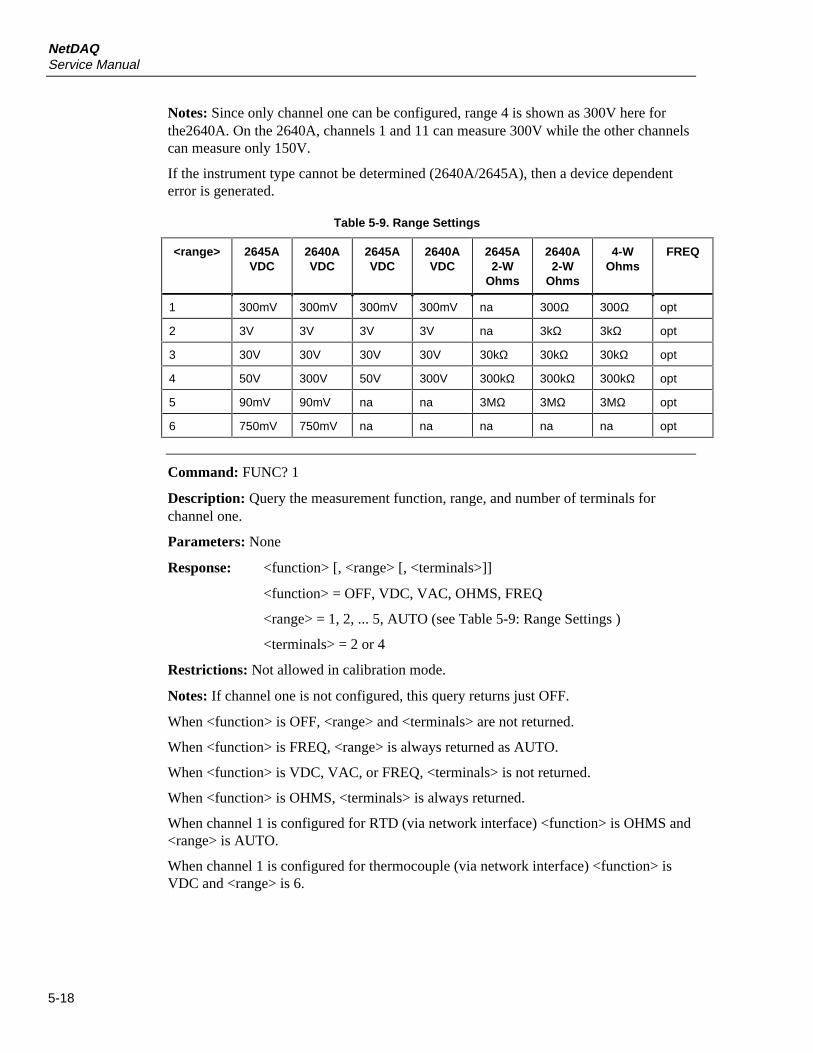
NetDAQService Manual
5-18
Notes: Since only channel one can be configured, range 4 is shown as 300V here forthe2640A. On the 2640A, channels 1 and 11 can measure 300V while the other channelscan measure only 150V.
If the instrument type cannot be determined (2640A/2645A), then a device dependenterror is generated.
Table 5-9. Range Settings
<range> 2645AVDC
2640AVDC
2645AVDC
2640AVDC
2645A2-W
Ohms
2640A2-W
Ohms
4-WOhms
FREQ
1 300mV 300mV 300mV 300mV na 300Ω 300Ω opt
2 3V 3V 3V 3V na 3kΩ 3kΩ opt
3 30V 30V 30V 30V 30kΩ 30kΩ 30kΩ opt
4 50V 300V 50V 300V 300kΩ 300kΩ 300kΩ opt
5 90mV 90mV na na 3MΩ 3MΩ 3MΩ opt
6 750mV 750mV na na na na na opt
Command: FUNC? 1
Description: Query the measurement function, range, and number of terminals forchannel one.
Parameters: None
Response: <function> [, <range> [, <terminals>]]
<function> = OFF, VDC, VAC, OHMS, FREQ
<range> = 1, 2, ... 5, AUTO (see Table 5-9: Range Settings )
<terminals> = 2 or 4
Restrictions: Not allowed in calibration mode.
Notes: If channel one is not configured, this query returns just OFF.
When <function> is OFF, <range> and <terminals> are not returned.
When <function> is FREQ, <range> is always returned as AUTO.
When <function> is VDC, VAC, or FREQ, <terminals> is not returned.
When <function> is OHMS, <terminals> is always returned.
When channel 1 is configured for RTD (via network interface) <function> is OHMS and<range> is AUTO.
When channel 1 is configured for thermocouple (via network interface) <function> isVDC and <range> is 6.
Diagnostic Testing and TroubleshootingTroubleshooting the Instrument 5
5-19
Command: MEAS?
Description: Takes a measurement on channel one and returns the measured value. Thiscommand is new to the instrument.
Parameters: None
Response: <measurement> = IEEE-488.2 NR3 ASCII representation of a floating pointvalue: leading sign;
5 or 6 digits with embedded decimal point for 2645A and 2640A respectively,padded
with leading and trailing zeroes if necessary;“E”;a signed exponent of -3, +0, +3, or +6.
For example +115.67E+0.
An overload condition is indicated by a value of +001.00E+9 or -001.00E+9 in the2645A, +001.000E+9 or -001.000E+9 for the 2640A.
Restrictions: Not allowed in calibration mode. If channel one is not configured, thiscommand generates an execution error and does not return a value.
Notes: While processing this query, the instrument does not return a response or aprompt until the measurement has been taken.
The instrument generates a device dependent error if the measurement does not arriveafter 30 seconds.
Open thermocouples return a +999.99[9]E+9.
Troubleshooting the Instrument 5-19.The following paragraphs describe an organized method of instrument troubleshooting.The overall approach is to start with power-up self-test error codes and then proceed tomore and more detailed procedures. Begin troubleshooting with “GeneralTroubleshooting.” These procedures locate about 90% of the instrument faults. Theremaining faults require sleuthing that is beyond the scope of this manual. For thesecases, review Chapter 2 “Theory of Operation” and approach the difficulty in a logicalmanner adapting the troubleshooting procedures, as required. As a last resort, contact thefactory or Fluke Service Center (see Chapter 6) for assistance.
General Troubleshooting 5-20.
General troubleshooting uses the instrument response to self-test as a clue to the faultlocation. If the instrument completes self-test and displays an error code on the frontpanel, refer to Table 5-10. If the instrument appears dead and will not even self test, referto Table 5-11. If the instrument passes self test but is not operating correctly, then referto “Troubleshooting the A3 A/D Converter PCA” for analog problems, and“Troubleshooting the A1 Main PCA” for digital problems. For assembly anddisassembly procedures, see Chapter 3, “General Maintenance.”
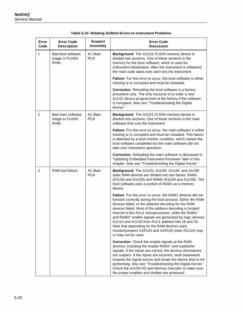
NetDAQService Manual
5-20
Table 5-10. Relating Selftest Errors to Instrument Problems
ErrorCode
Error CodeDescription
SuspectAssembly
Error CodeDiscussion
1 Bad boot softwareimage in FLASHROM.
A1 MainPCA
Background The A1U21 FLASH memory device isdivided into sections. One of these sections is thememory for the boot software, which is used forinstrument initialization. After the instrument is initialized,the main code takes over and runs the instrument.
Failure For this error to occur, the boot software is eithermissing or is corrupted and must be reloaded.
Correction Reloading the boot software is a factoryprocedure only. The only recourse is to order a newA1U21 device programmed at the factory if the softwareis corrupted. Also see “Troubleshooting the DigitalKernel.”
2 Bad main softwareimage in FLASHROM.
A1 MainPCA
Background The A1U21 FLASH memory device isdivided into sections. One of these sections is the mainsoftware that runs the instrument.
Failure For this error to occur, the main software is eithermissing or is corrupted and must be reloaded. This failureis detected by a boot monitor condition, which means theboot software completed but the main software did nottake over instrument operation.
Correction Reloading the main software is discussed in“Updating Embedded Instrument Firmware” later in thischapter. Also see “Troubleshooting the Digital Kernel.”
3 RAM test failure. A1 MainPCA
Background The A1U20, A1U30, A1U34, and A1U35static RAM devices are divided into two banks: RAM1(A1U20 and A1U30) and RAM2 (A1U34 and A1U35). Theboot software uses a portion of RAM1 as a memorydevice.
Failure For this error to occur, the RAM1 devices did notfunction correctly during the boot process. Either the RAMdevices failed, or the address decoding for the RAMdevices failed. Most of the address decoding is locatedinternal to the A1U1 microprocessor, while the RAM1*and RAM2* enable signals are generated by logic devicesA1U14 and A1U15 from A1U1 address bits 18 and 20.Note that depending on the RAM devices used,resistor/jumpers A1R125 and A1R126 (near A1U14) mayor may not be used.
Correction Check the enable signals at the RAMdevices, including the enable RAM1* and read/writesignals. If the inputs are correct, the devices themselvesare suspect. If the inputs are incorrect, work backwardstowards the signal source and locate the device that is notperforming. Also see “Troubleshooting the Digital Kernel.”Check the A1U29 I/O and Memory Decoder to make surethe proper enables and strobes are produced.
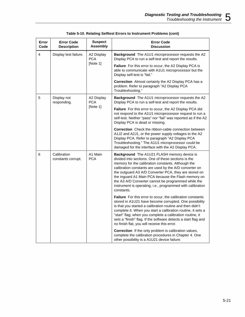
Diagnostic Testing and TroubleshootingTroubleshooting the Instrument 5
5-21
Table 5-10. Relating Selftest Errors to Instrument Problems (cont)
ErrorCode
Error CodeDescription
SuspectAssembly
Error CodeDiscussion
4 Display test failure. A2 DisplayPCA[Note 1]
Background The A1U1 microprocessor requests the A2Display PCA to run a self-test and report the results.
Failure For this error to occur, the A2 Display PCA isable to communicate with A1U1 microprocessor but theDisplay self-test is “fail.”
Correction Almost certainly the A2 Display PCA has aproblem. Refer to paragraph “A2 Display PCATroubleshooting.”
5 Display notresponding.
A2 DisplayPCA[Note 1]
Background The A1U1 microprocessor requests the A2Display PCA to run a self-test and report the results.
Failure For this error to occur, the A2 Display PCA didnot respond to the A1U1 microprocessor request to run aself-test. Neither “pass” nor “fail” was reported as if the A2Display PCA is dead or missing.
Correction Check the ribbon-cable connection betweenA1J2 and A2J1, or the power supply voltages to the A2Display PCA. Refer to paragraph “A2 Display PCATroubleshooting.” The A1U1 microprocessor could bedamaged for the interface with the A2 Display PCA.
6 Calibrationconstants corrupt.
A1 MainPCA
Background The A1U21 FLASH memory device isdivided into sections. One of these sections is thememory for the calibration constants. Although thecalibration constants are used by the A/D converter onthe outguard A3 A/D Converter PCA, they are stored onthe inguard A1 Main PCA because the Flash memory onthe A3 A/D Converter cannot be programmed while theinstrument is operating, i.e., programmed with calibrationconstants.
Failure For this error to occur, the calibration constantsstored in A1U21 have become corrupted. One possibilityis that you started a calibration routine and then didn’tcomplete it. When you start a calibration routine, it sets a“start” flag; when you complete a calibration routine, itsets a “finish” flag. If the software detects a start flag andno finish flat, you will receive this error.
Correction If the only problem is calibration values,complete the calibration procedures in Chapter 4. Oneother possibility is a A1U21 device failure.
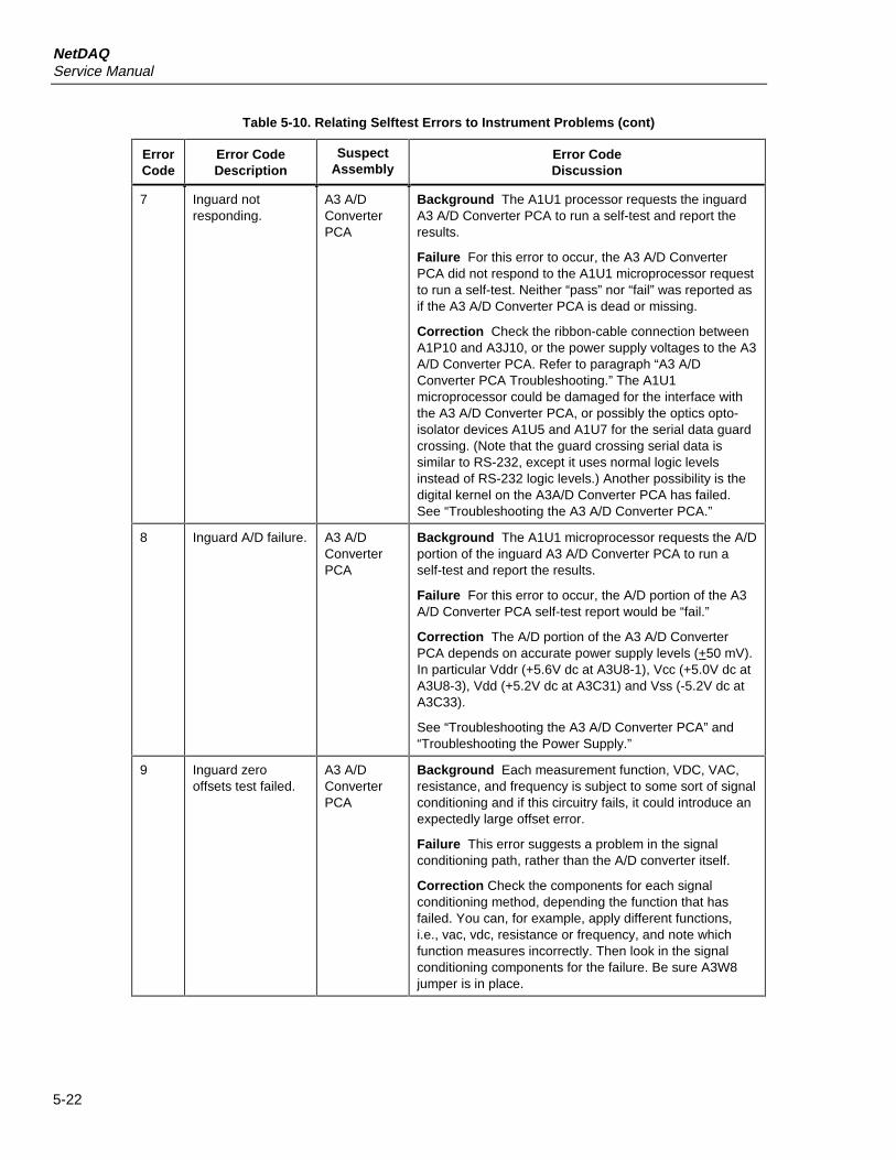
NetDAQService Manual
5-22
Table 5-10. Relating Selftest Errors to Instrument Problems (cont)
ErrorCode
Error CodeDescription
SuspectAssembly
Error CodeDiscussion
7 Inguard notresponding.
A3 A/DConverterPCA
Background The A1U1 processor requests the inguardA3 A/D Converter PCA to run a self-test and report theresults.
Failure For this error to occur, the A3 A/D ConverterPCA did not respond to the A1U1 microprocessor requestto run a self-test. Neither “pass” nor “fail” was reported asif the A3 A/D Converter PCA is dead or missing.
Correction Check the ribbon-cable connection betweenA1P10 and A3J10, or the power supply voltages to the A3A/D Converter PCA. Refer to paragraph “A3 A/DConverter PCA Troubleshooting.” The A1U1microprocessor could be damaged for the interface withthe A3 A/D Converter PCA, or possibly the optics opto-isolator devices A1U5 and A1U7 for the serial data guardcrossing. (Note that the guard crossing serial data issimilar to RS-232, except it uses normal logic levelsinstead of RS-232 logic levels.) Another possibility is thedigital kernel on the A3A/D Converter PCA has failed.See “Troubleshooting the A3 A/D Converter PCA.”
8 Inguard A/D failure. A3 A/DConverterPCA
Background The A1U1 microprocessor requests the A/Dportion of the inguard A3 A/D Converter PCA to run aself-test and report the results.
Failure For this error to occur, the A/D portion of the A3A/D Converter PCA self-test report would be “fail.”
Correction The A/D portion of the A3 A/D ConverterPCA depends on accurate power supply levels (+50 mV). In particular Vddr (+5.6V dc at A3U8-1), Vcc (+5.0V dc atA3U8-3), Vdd (+5.2V dc at A3C31) and Vss (-5.2V dc atA3C33).
See “Troubleshooting the A3 A/D Converter PCA” and“Troubleshooting the Power Supply.”
9 Inguard zerooffsets test failed.
A3 A/DConverterPCA
Background Each measurement function, VDC, VAC,resistance, and frequency is subject to some sort of signalconditioning and if this circuitry fails, it could introduce anexpectedly large offset error.
Failure This error suggests a problem in the signalconditioning path, rather than the A/D converter itself.
Correction Check the components for each signalconditioning method, depending the function that hasfailed. You can, for example, apply different functions,i.e., vac, vdc, resistance or frequency, and note whichfunction measures incorrectly. Then look in the signalconditioning components for the failure. Be sure A3W8jumper is in place.
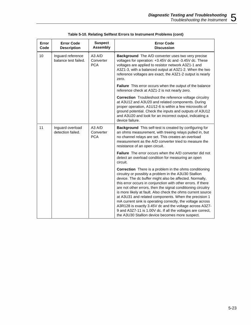
Diagnostic Testing and TroubleshootingTroubleshooting the Instrument 5
5-23
Table 5-10. Relating Selftest Errors to Instrument Problems (cont)
ErrorCode
Error CodeDescription
SuspectAssembly
Error CodeDiscussion
10 Inguard referencebalance test failed.
A3 A/DConverterPCA
Background The A/D converter uses two very precisevoltages for operation: +3.45V dc and -3.45V dc. Thesevoltages are applied to resistor network A3Z1-1 andA3Z1-3, with a balanced output at A3Z1-2. When the tworeference voltages are exact, the A3Z1-2 output is nearlyzero.
Failure This error occurs when the output of the balancereference check at A3Z1-2 is not nearly zero.
Correction Troubleshoot the reference voltage circuitryat A3U12 and A3U20 and related components. Duringproper operation, A1U12-6 is within a few microvolts ofground potential. Check the inputs and outputs of A3U12and A3U20 and look for an incorrect output, indicating adevice failure.
11 Inguard overloaddetection failed.
A3 A/DConverterPCA
Background This self-test is created by configuring foran ohms measurement, with treeing relays pulled in, butno channel relays are set. This creates an overloadmeasurement as the A/D converter tried to measure theresistance of an open circuit.
Failure The error occurs when the A/D converter did notdetect an overload condition for measuring an opencircuit.
Correction There is a problem in the ohms conditioningcircuitry or possibly a problem in the A3U30 Stalliondevice. The dc buffer might also be affected. Normally,this error occurs in conjunction with other errors. If thereare not other errors, then the signal conditioning circuitryis more likely at fault. Also check the ohms current sourceat A3U31 and related components. When the precision 1mA current sink is operating correctly, the voltage acrossA3R128 is exactly 3.45V dc and the voltage across A3Z7-9 and A3Z7-11 is 1.00V dc. If all the voltages are correct,the A3U30 Stallion device becomes more suspect.
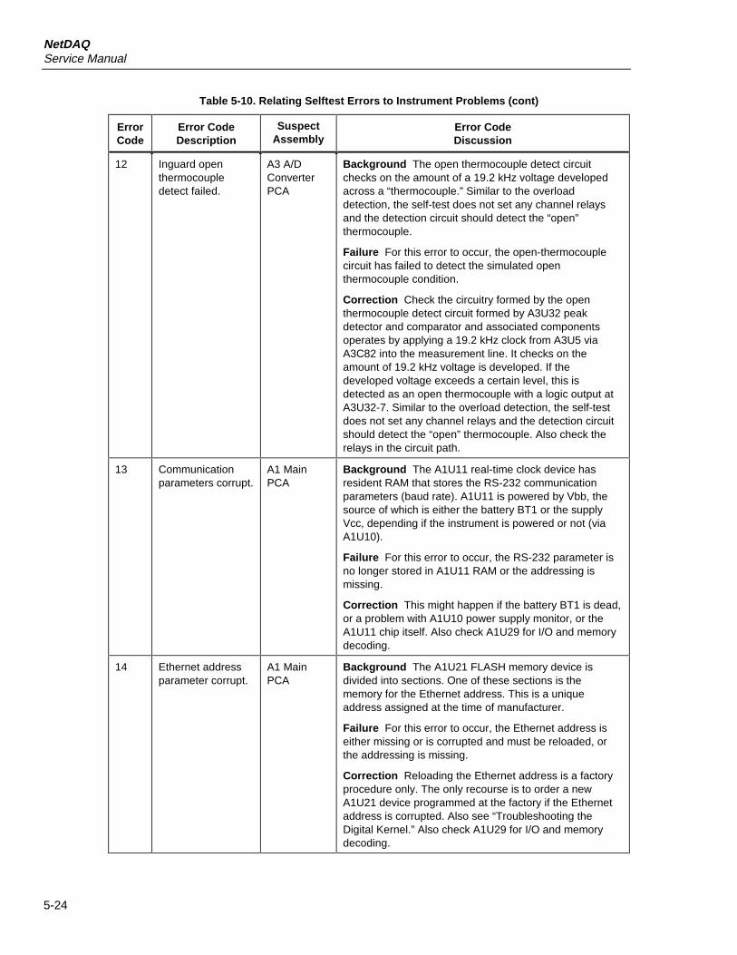
NetDAQService Manual
5-24
Table 5-10. Relating Selftest Errors to Instrument Problems (cont)
ErrorCode
Error CodeDescription
SuspectAssembly
Error CodeDiscussion
12 Inguard openthermocoupledetect failed.
A3 A/DConverterPCA
Background The open thermocouple detect circuitchecks on the amount of a 19.2 kHz voltage developedacross a “thermocouple.” Similar to the overloaddetection, the self-test does not set any channel relaysand the detection circuit should detect the “open”thermocouple.
Failure For this error to occur, the open-thermocouplecircuit has failed to detect the simulated openthermocouple condition.
Correction Check the circuitry formed by the openthermocouple detect circuit formed by A3U32 peakdetector and comparator and associated componentsoperates by applying a 19.2 kHz clock from A3U5 viaA3C82 into the measurement line. It checks on theamount of 19.2 kHz voltage is developed. If thedeveloped voltage exceeds a certain level, this isdetected as an open thermocouple with a logic output atA3U32-7. Similar to the overload detection, the self-testdoes not set any channel relays and the detection circuitshould detect the “open” thermocouple. Also check therelays in the circuit path.
13 Communicationparameters corrupt.
A1 MainPCA
Background The A1U11 real-time clock device hasresident RAM that stores the RS-232 communicationparameters (baud rate). A1U11 is powered by Vbb, thesource of which is either the battery BT1 or the supplyVcc, depending if the instrument is powered or not (viaA1U10).
Failure For this error to occur, the RS-232 parameter isno longer stored in A1U11 RAM or the addressing ismissing.
Correction This might happen if the battery BT1 is dead,or a problem with A1U10 power supply monitor, or theA1U11 chip itself. Also check A1U29 for I/O and memorydecoding.
14 Ethernet addressparameter corrupt.
A1 MainPCA
Background The A1U21 FLASH memory device isdivided into sections. One of these sections is thememory for the Ethernet address. This is a uniqueaddress assigned at the time of manufacturer.
Failure For this error to occur, the Ethernet address iseither missing or is corrupted and must be reloaded, orthe addressing is missing.
Correction Reloading the Ethernet address is a factoryprocedure only. The only recourse is to order a newA1U21 device programmed at the factory if the Ethernetaddress is corrupted. Also see “Troubleshooting theDigital Kernel.” Also check A1U29 for I/O and memorydecoding.
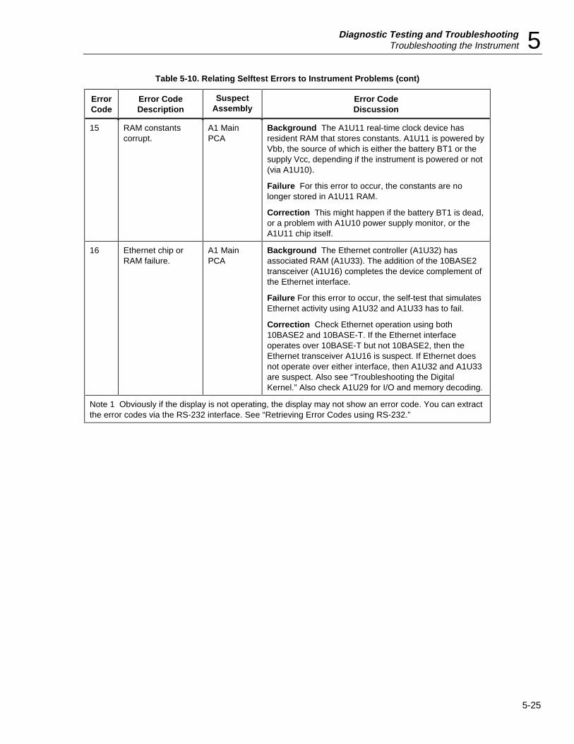
Diagnostic Testing and TroubleshootingTroubleshooting the Instrument 5
5-25
Table 5-10. Relating Selftest Errors to Instrument Problems (cont)
ErrorCode
Error CodeDescription
SuspectAssembly
Error CodeDiscussion
15 RAM constantscorrupt.
A1 MainPCA
Background The A1U11 real-time clock device hasresident RAM that stores constants. A1U11 is powered byVbb, the source of which is either the battery BT1 or thesupply Vcc, depending if the instrument is powered or not(via A1U10).
Failure For this error to occur, the constants are nolonger stored in A1U11 RAM.
Correction This might happen if the battery BT1 is dead,or a problem with A1U10 power supply monitor, or theA1U11 chip itself.
16 Ethernet chip orRAM failure.
A1 MainPCA
Background The Ethernet controller (A1U32) hasassociated RAM (A1U33). The addition of the 10BASE2transceiver (A1U16) completes the device complement ofthe Ethernet interface.
Failure For this error to occur, the self-test that simulatesEthernet activity using A1U32 and A1U33 has to fail.
Correction Check Ethernet operation using both10BASE2 and 10BASE-T. If the Ethernet interfaceoperates over 10BASE-T but not 10BASE2, then theEthernet transceiver A1U16 is suspect. If Ethernet doesnot operate over either interface, then A1U32 and A1U33are suspect. Also see “Troubleshooting the DigitalKernel.” Also check A1U29 for I/O and memory decoding.
Note 1 Obviously if the display is not operating, the display may not show an error code. You can extractthe error codes via the RS-232 interface. See “Retrieving Error Codes using RS-232.”
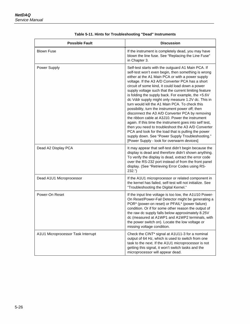
NetDAQService Manual
5-26
Table 5-11. Hints for Troubleshooting "Dead" Instruments
Possible Fault Discussion
Blown Fuse If the instrument is completely dead, you may haveblown the line fuse. See “Replacing the Line Fuse”in Chapter 3.
Power Supply Self-test starts with the outguard A1 Main PCA. Ifself-test won’t even begin, then something is wrongeither at the A1 Main PCA or with a power supplyvoltage. If the A3 A/D Converter PCA has a shortcircuit of some kind, it could load down a powersupply voltage such that the current limiting featureis folding the supply back. For example, the +5.6Vdc Vddr supply might only measure 1.2V dc. This inturn would kill the A1 Main PCA. To check thispossibility, turn the instrument power off; thendisconnect the A3 A/D Converter PCA by removingthe ribbon cable at A3J10. Power the instrumentagain. If this time the instrument goes into self test,then you need to troubleshoot the A3 A/D ConverterPCA and look for the load that is pulling the powersupply down. See “Power Supply Troubleshooting.”[Power Supply - look for overwarm devices]
Dead A2 Display PCA It may appear that self-test didn’t begin because thedisplay is dead and therefore didn’t shown anything.To verify the display is dead, extract the error codeover the RS-232 port instead of from the front paneldisplay. (See “Retrieving Error Codes using RS-232.”)
Dead A1U1 Microprocessor If the A1U1 microprocessor or related component inthe kernel has failed, self-test will not initialize. See“Troubleshooting the Digital Kernel.”
Power-On Reset If the input line voltage is too low, the A1U10 Power-On Reset/Power-Fail Detector might be generating aPOR* (power-on reset) or PFAIL* (power failure)condition. Or if for some other reason the output ofthe raw dc supply falls below approximately 8.25Vdc (measured at A1WP1 and A1WP2 terminals, withthe power switch on). Locate the low voltage ormissing voltage condition.
A1U1 Microprocessor Task Interrupt Check the CINT* signal at A1U11-3 for a nominaloutput of 64 Hz, which is used to switch from onetask to the next. If the A1U1 microprocessor is notgetting this signal, it won’t switch tasks and themicroprocessor will appear dead.
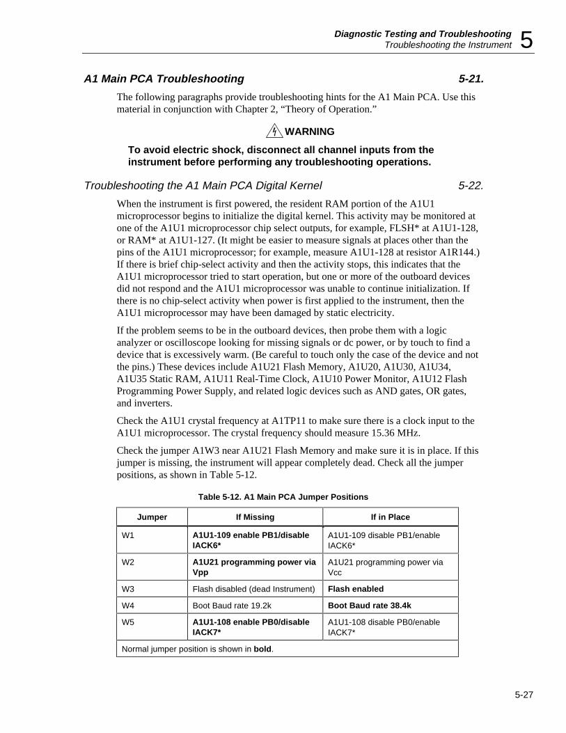
Diagnostic Testing and TroubleshootingTroubleshooting the Instrument 5
5-27
A1 Main PCA Troubleshooting 5-21.
The following paragraphs provide troubleshooting hints for the A1 Main PCA. Use thismaterial in conjunction with Chapter 2, “Theory of Operation.”
WARNING
To avoid electric shock, disconnect all channel inputs from theinstrument before performing any troubleshooting operations.
Troubleshooting the A1 Main PCA Digital Kernel 5-22.
When the instrument is first powered, the resident RAM portion of the A1U1microprocessor begins to initialize the digital kernel. This activity may be monitored atone of the A1U1 microprocessor chip select outputs, for example, FLSH* at A1U1-128,or RAM* at A1U1-127. (It might be easier to measure signals at places other than thepins of the A1U1 microprocessor; for example, measure A1U1-128 at resistor A1R144.)If there is brief chip-select activity and then the activity stops, this indicates that theA1U1 microprocessor tried to start operation, but one or more of the outboard devicesdid not respond and the A1U1 microprocessor was unable to continue initialization. Ifthere is no chip-select activity when power is first applied to the instrument, then theA1U1 microprocessor may have been damaged by static electricity.
If the problem seems to be in the outboard devices, then probe them with a logicanalyzer or oscilloscope looking for missing signals or dc power, or by touch to find adevice that is excessively warm. (Be careful to touch only the case of the device and notthe pins.) These devices include A1U21 Flash Memory, A1U20, A1U30, A1U34,A1U35 Static RAM, A1U11 Real-Time Clock, A1U10 Power Monitor, A1U12 FlashProgramming Power Supply, and related logic devices such as AND gates, OR gates,and inverters.
Check the A1U1 crystal frequency at A1TP11 to make sure there is a clock input to theA1U1 microprocessor. The crystal frequency should measure 15.36 MHz.
Check the jumper A1W3 near A1U21 Flash Memory and make sure it is in place. If thisjumper is missing, the instrument will appear completely dead. Check all the jumperpositions, as shown in Table 5-12.
Table 5-12. A1 Main PCA Jumper Positions
Jumper If Missing If in Place
W1 A1U1-109 enable PB1/disableIACK6*
A1U1-109 disable PB1/enableIACK6*
W2 A1U21 programming power viaVpp
A1U21 programming power viaVcc
W3 Flash disabled (dead Instrument) Flash enabled
W4 Boot Baud rate 19.2k Boot Baud rate 38.4k
W5 A1U1-108 enable PB0/disableIACK7*
A1U1-108 disable PB0/enableIACK7*
Normal jumper position is shown in bold.
NetDAQService Manual
5-28
Check that no programming power is applied to A1U21-1 Flash Memory (+12V dc).Programming power is applied only when storing (for example) calibration constants.During normal operation, A1U21-1 should not be powered. If power is being applied toA1U21-1 during normal operation, check to make sure jumper A1W2 is not in place (seeTable 5-12) and probe A1U12 to find the cause for the presence of Vpp.
Check A1U29 I/O and Memory Decoder. If this device is not responding correctly, awhole host of address problems will occur, including RAM and Flash write and readstrobes. A failure of this device would result in several error code reports.
Troubleshooting the RS-232 Interface 5-23.
If the instrument RS-232 port does not seem to operate, be sure you have selected thecorrect RS-232 baud rate for the interface with a terminal or PC running terminalemulation software. If everything seems to be correct, troubleshoot the RS-232 interfaceA1U13 drivers, in particular, A1TP12 for the receive (RX) input.
Troubleshooting the Ethernet Interface 5-24.
If Ethernet operates on 10BASE-T but not 10BASE2, the A1U16 transceiver is suspect.Check pin A1U16-18 for a nominal -7V dc and A1U16-19 for a nominal -8V dc. Sincethe A1U16 device is powered by power supply module A1U38, you should also checkA1U38 for the correct output of -9V dc. Also check A1U2, which processes the A1U32Ethernet Controller interrupt output. Finally, if there still is an Ethernet problem, thefault could be caused by the A1U32 Ethernet Controller itself or its associated RAMdevice, A1U33. One check is to measure the bias voltage at A1U32-21 (at resistorA1R107). For a normally operating A1U32 device, this voltage is a nominal +1.22V dc.
Troubleshooting the Digital I/O Lines and Trigger Out Lines 5-25.
When the instrument is powered, the A1U31 Field Programmable Gate Array isprogrammed by the A1U1 microprocessor as part of the initialization routine. Thusprogrammed, the FPGA interfaces with the keys portion of the A2 Display PCA and theDIO lines such as the instrument rear panel DIGITAL I/O dio7 to dio0, as well as thetrigger output and input lines. If there are any problems in this area, check the A1U31signal conditions, in particular, the D-clock output at A1U31-19. If all appears well,check the associated receivers A1U3 and A1U4, and drivers A1U17 and A1U27. Often ifa receiver or driver device fails, you will lose a block of dio lines. Power supply voltagelevels are important here because of threshold levels. Check the power supply voltages.Note that the fanout for the trigger output line is increased by A1Q10 so that this outputcan be connected to 20 trigger input lines without overloading the signal. If there areproblems with loading of the trigger output line, check A1Q10.
Troubleshooting the Totalizer and Trigger In Lines 5-26.
The Totalizer and Trigger In inputs are processed by A1U8 and associated devices, andapplied to the A1U31 FPGA. If you have problems with these features, check for thecorrection inputs to the FPGA. If the inputs are correct, then the FPGA is suspect or theprogramming of the FPGA is suspect.
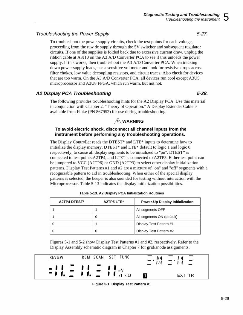
Diagnostic Testing and TroubleshootingTroubleshooting the Instrument 5
5-29
Troubleshooting the Power Supply 5-27.
To troubleshoot the power supply circuits, check the test points for each voltage,proceeding from the raw dc supply through the 5V switcher and subsequent regulatorcircuits. If one of the supplies is folded back due to excessive current draw, unplug theribbon cable at A3J10 on the A3 A/D Converter PCA to see if this unloads the powersupply. If this works, then troubleshoot the A3 A/D Converter PCA. When trackingdown power supply loads, use a sensitive voltmeter and look for resistive drops acrossfilter chokes, low value decoupling resistors, and circuit traces. Also check for devicesthat are too warm. On the A3 A/D Converter PCA, all devices run cool except A3U5microprocessor and A3U8 FPGA, which run warm, but not hot.
A2 Display PCA Troubleshooting 5-28.
The following provides troubleshooting hints for the A2 Display PCA. Use this materialin conjunction with Chapter 2, “Theory of Operation.” A Display Extender Cable isavailable from Fluke (PN 867952) for use during troubleshooting.
WARNING
To avoid electric shock, disconnect all channel inputs from theinstrument before performing any troubleshooting operations.
The Display Controller reads the DTEST* and LTE* inputs to determine how toinitialize the display memory. DTEST* and LTE* default to logic 1 and logic 0,respectively, to cause all display segments to be initialized to "on". DTEST* isconnected to test points A2TP4, and LTE* is connected to A2TP5. Either test point canbe jumpered to VCC (A2TP6) or GND (A2TP3) to select other display initializationpatterns. Display Test Patterns #1 and #2 are a mixture of "on" and "off" segments with arecognizable pattern to aid in troubleshooting. When either of the special displaypatterns is selected, the beeper is also sounded for testing without interaction with theMicroprocessor. Table 5-13 indicates the display initialization possibilities.
Table 5-13. A2 Display PCA Initialization Routines
A2TP4 DTEST* A2TP5 LTE* Power-Up Display Initialization
1 1 All segments OFF
1 0 All segments ON (default)
0 1 Display Test Pattern #1
0 0 Display Test Pattern #2
Figures 5-1 and 5-2 show Display Test Patterns #1 and #2, respectively. Refer to theDisplay Assembly schematic diagram in Chapter 7 for grid/anode assignments.
REVIEW REM SCAN
x1 k EXT
SET FUNC
mV TR1Ω
Figure 5-1. Display Test Pattern #1
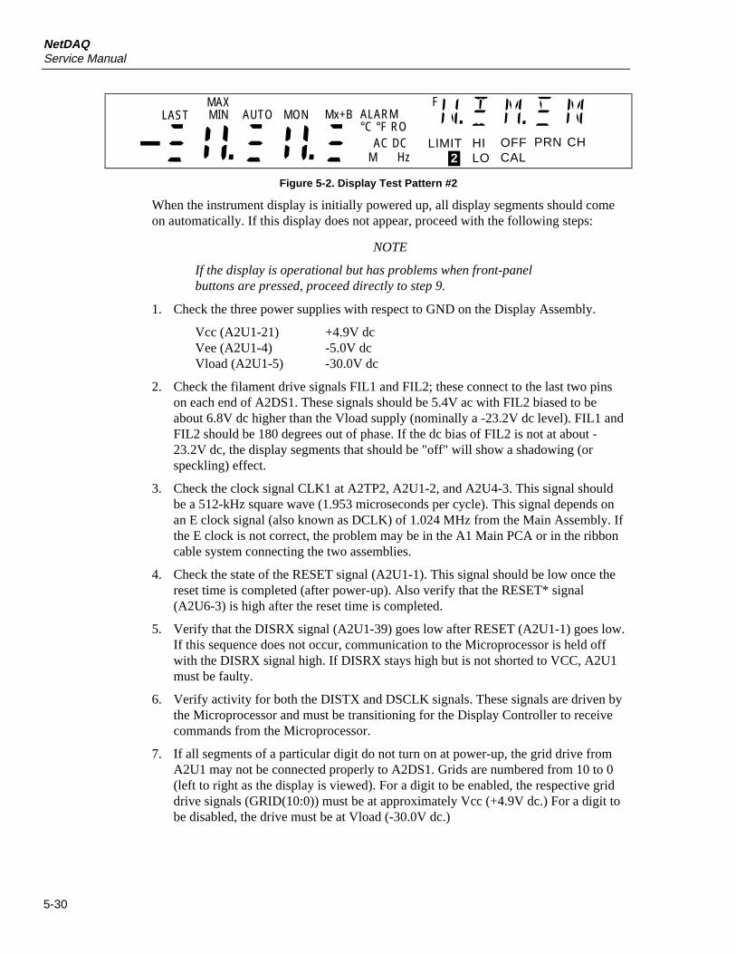
NetDAQService Manual
5-30
LASTMAXMIN AUTO MON
MLIMIT HI
LOOFFCAL
PRN
Mx+B ALARM°C °F RO
AC DCHz
CH2
F
Figure 5-2. Display Test Pattern #2
When the instrument display is initially powered up, all display segments should comeon automatically. If this display does not appear, proceed with the following steps:
NOTE
If the display is operational but has problems when front-panelbuttons are pressed, proceed directly to step 9.
1. Check the three power supplies with respect to GND on the Display Assembly.
Vcc (A2U1-21) +4.9V dcVee (A2U1-4) -5.0V dcVload (A2U1-5) -30.0V dc
2. Check the filament drive signals FIL1 and FIL2; these connect to the last two pinson each end of A2DS1. These signals should be 5.4V ac with FIL2 biased to beabout 6.8V dc higher than the Vload supply (nominally a -23.2V dc level). FIL1 andFIL2 should be 180 degrees out of phase. If the dc bias of FIL2 is not at about -23.2V dc, the display segments that should be "off" will show a shadowing (orspeckling) effect.
3. Check the clock signal CLK1 at A2TP2, A2U1-2, and A2U4-3. This signal shouldbe a 512-kHz square wave (1.953 microseconds per cycle). This signal depends onan E clock signal (also known as DCLK) of 1.024 MHz from the Main Assembly. Ifthe E clock is not correct, the problem may be in the A1 Main PCA or in the ribboncable system connecting the two assemblies.
4. Check the state of the RESET signal (A2U1-1). This signal should be low once thereset time is completed (after power-up). Also verify that the RESET* signal(A2U6-3) is high after the reset time is completed.
5. Verify that the DISRX signal (A2U1-39) goes low after RESET (A2U1-1) goes low.If this sequence does not occur, communication to the Microprocessor is held offwith the DISRX signal high. If DISRX stays high but is not shorted to VCC, A2U1must be faulty.
6. Verify activity for both the DISTX and DSCLK signals. These signals are driven bythe Microprocessor and must be transitioning for the Display Controller to receivecommands from the Microprocessor.
7. If all segments of a particular digit do not turn on at power-up, the grid drive fromA2U1 may not be connected properly to A2DS1. Grids are numbered from 10 to 0(left to right as the display is viewed). For a digit to be enabled, the respective griddrive signals (GRID(10:0)) must be at approximately Vcc (+4.9V dc.) For a digit tobe disabled, the drive must be at Vload (-30.0V dc.)
Diagnostic Testing and TroubleshootingTroubleshooting the Instrument 5
5-31
8. If a segment under each of several (or all) grids fails to be turned on (or off)properly, one of the anode drive signals may not be connected properly from A2U1to A2DS1. When an anode signal is at Vcc, and a grid signal is at Vcc, thecorresponding segment on the display is illuminated.
9. If the Microprocessor has difficulty recognizing front-panel button presses, theswitch scanning signals SWR1 through SWR6 should be checked. When no switchcontacts are being closed, the switch scanning lines should have about 20 kΩ ofresistance between each other (through two 10 kΩ pull-up resistors to Vcc). Unlessone of the switches is closed, none of the switch scanning lines should be shorteddirectly to GND at any time.
Variations in the Display 5-29.
Under normal operation, the display presents various combinations of brightly and dimlylit annunciators and digits. However, you may encounter other, random irregularitiesacross different areas of the display under the following circumstances:
• After prolonged periods of displaying the same information.
• If the display has not been used for a prolonged period.
This phenomenon can be cleared by activating the entire display and leaving it onovernight (or at least for several hours). Use the following procedure to keep the displayfully lit:
1. With power OFF, press and hold the left arrow key, then press power ON.
2. Wait a moment for the instrument to beep, then release the key. The entire displaywill now stay on until you are ready to deactivate it.
3. At the end of the activation period, press any button on the front panel; theinstrument resumes the mode in effect prior to the power interruption (Active orInactive.)
A3 A/D Converter PCA Troubleshooting 5-30.
The following paragraphs provide troubleshooting hints for the A3 A/D Converter PCA.Use this material in conjunction with Chapter 2, “Theory of Operation.”
WARNING
To avoid electric shock, disconnect all channel inputs from theinstrument before performing any troubleshooting operations.
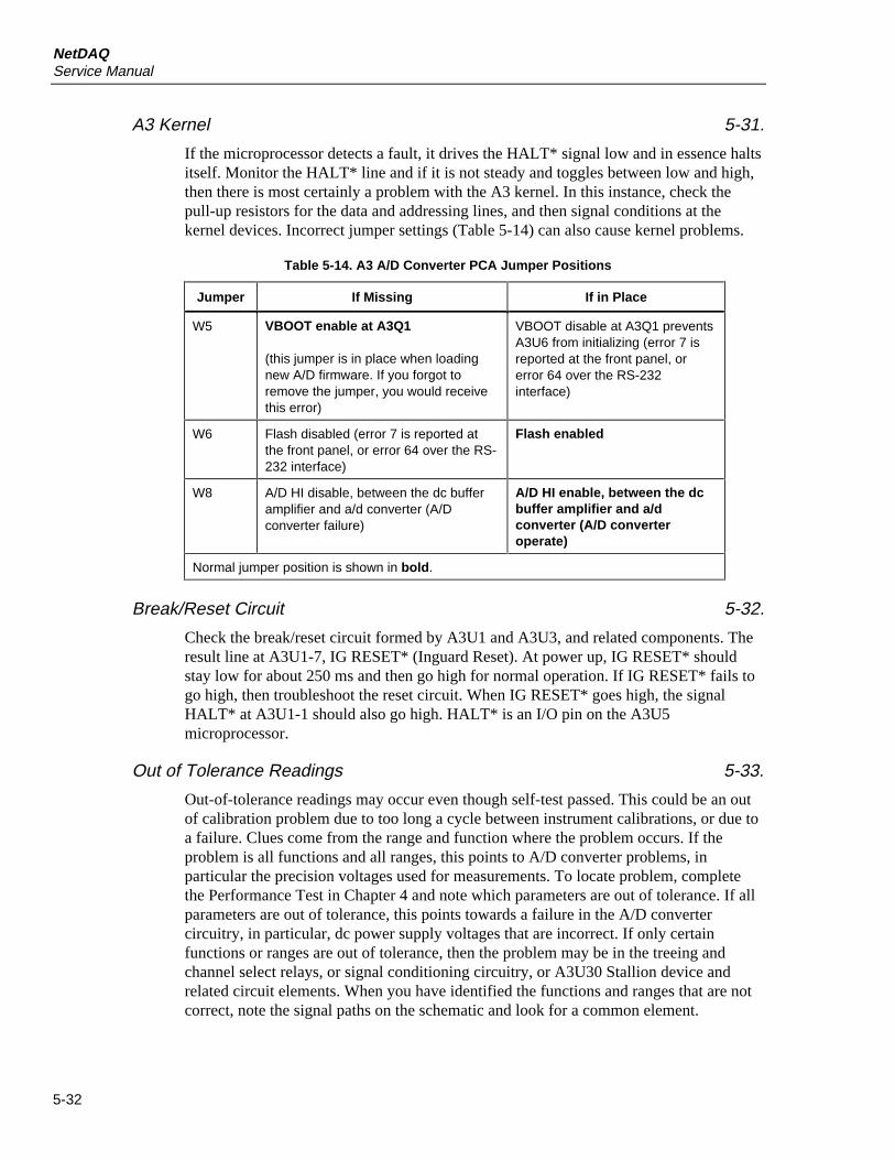
NetDAQService Manual
5-32
A3 Kernel 5-31.
If the microprocessor detects a fault, it drives the HALT* signal low and in essence haltsitself. Monitor the HALT* line and if it is not steady and toggles between low and high,then there is most certainly a problem with the A3 kernel. In this instance, check thepull-up resistors for the data and addressing lines, and then signal conditions at thekernel devices. Incorrect jumper settings (Table 5-14) can also cause kernel problems.
Table 5-14. A3 A/D Converter PCA Jumper Positions
Jumper If Missing If in Place
W5 VBOOT enable at A3Q1
(this jumper is in place when loadingnew A/D firmware. If you forgot toremove the jumper, you would receivethis error)
VBOOT disable at A3Q1 preventsA3U6 from initializing (error 7 isreported at the front panel, orerror 64 over the RS-232interface)
W6 Flash disabled (error 7 is reported atthe front panel, or error 64 over the RS-232 interface)
Flash enabled
W8 A/D HI disable, between the dc bufferamplifier and a/d converter (A/Dconverter failure)
A/D HI enable, between the dcbuffer amplifier and a/dconverter (A/D converteroperate)
Normal jumper position is shown in bold.
Break/Reset Circuit 5-32.
Check the break/reset circuit formed by A3U1 and A3U3, and related components. Theresult line at A3U1-7, IG RESET* (Inguard Reset). At power up, IG RESET* shouldstay low for about 250 ms and then go high for normal operation. If IG RESET* fails togo high, then troubleshoot the reset circuit. When IG RESET* goes high, the signalHALT* at A3U1-1 should also go high. HALT* is an I/O pin on the A3U5microprocessor.
Out of Tolerance Readings 5-33.
Out-of-tolerance readings may occur even though self-test passed. This could be an outof calibration problem due to too long a cycle between instrument calibrations, or due toa failure. Clues come from the range and function where the problem occurs. If theproblem is all functions and all ranges, this points to A/D converter problems, inparticular the precision voltages used for measurements. To locate problem, completethe Performance Test in Chapter 4 and note which parameters are out of tolerance. If allparameters are out of tolerance, this points towards a failure in the A/D convertercircuitry, in particular, dc power supply voltages that are incorrect. If only certainfunctions or ranges are out of tolerance, then the problem may be in the treeing andchannel select relays, or signal conditioning circuitry, or A3U30 Stallion device andrelated circuit elements. When you have identified the functions and ranges that are notcorrect, note the signal paths on the schematic and look for a common element.
Diagnostic Testing and TroubleshootingTroubleshooting the Instrument 5
5-33
For dc volt problems that affect all channels, look for faults in the dc buffer and Stalliondevice. For dc volt problems on individual channels or groups of channels, check thechannel select (2640A only) and treeing relays.
For resistance problems, check the dc volts characteristics first. If there are no problems,then the difficulty is not in the dc buffer circuitry. This would suggest a problem in theohms conditioning circuit or the A3U30 Stallion device.
For ac volt problems, check the dc volts characteristics first. If there are no problems,then the difficulty is probably in the ac-to-dc conversion circuitry.
Troubleshooting Relay Problems 5-34.
Both the 2640A and 2645A use mechanical reed relays for signal switching, although the2645A uses solid-state relays for channel selection. The mechanical relays have a life of100,000,000 operations. If you use your instrument in long-duration, high-speedmeasurement runs at high voltages and high common mode voltages, then the relays maystart to act up after a few years. This includes failure to open, failure to close, excessivecontact resistance, and so forth. If your instrument is not subject to these extremes, thenrelay failures become less likely. An example of a relay failure is when the reading onone channel affects the readings on another channel (beyond the normal effects of cross-talk for ac measurements). This is especially true for dc volts, resistance, orthermocouple measurements. If a group of channels is causing problems, particular forchannels 1 to 10, and 11 to 20, then it may be a bus problem (bank1 and bank2). If thebanks are interacting, the treeing relays A3K21 to A3K24 may be at fault. You may findit easier to measure relay conditions by removing the A3 A/D Converter PCA andmeasuring at the bottom of the pca. However, removing the pca could unstick a stuckrelay and complicate relay troubleshooting. Also, for relay troubleshooting, applying+1V dc to the even channels and -1V dc to the odd channels can assist you in signaltracing. Crossed relays, for example, might cause a 0V reading where you expected +1V.
A4 Analog Input PCA Troubleshooting 5-35.
The A4 Analog Input PCA is essentially a passive assembly of terminal blocks, with theexception of a small active network formed around A4Q1 that provides a temperaturereference for thermocouple measurements. If thermocouple measurements are out oftolerance, A4Q1 may be suspect.
To verify the operation of A4Q1, connect multimeter test leads across A4R2 (markedand clearly visible in the open module) and power the instrument. At normal roomtemperatures, the voltage across A4R2 is a nominal 1V dc. If the measured voltage is0V, A4Q1 is probably open and should be replaced. For this test, you may find it easierif you remove the cover portion of the Universal Input Module by gently lifting one ofthe tabs the form the cover hinge and removing the cover.
WARNING
To avoid electric shock, disconnect all channel inputs from theinstrument before performing any troubleshooting operations.
The A4Q1 circuit is calibrated at the factory by adjusting the potentiometer A4R3. Donot disturb this adjustment unless you have replaced A4Q1. If you have replaced A4Q1,allow the instrument to stabilize in an ambient temperature of exactly 22*C and thenadjust A4R3 for a reading of 1.00V dc across A4R2.
NetDAQService Manual
5-34
Troubleshooting Calibration Failures 5-36.The paragraphs in this section describe troubleshooting actions when there is acalibration failure. Calibration procedures are provided in Chapter 4.
Calibration of the instrument through the computer interface is described in Chapter 4 ofthis manual. Generally, a calibration failure is indicated by a Device Dependent Errorand a "!>" prompt after a CAL_STEP? command. These indications occur if the analoginput varies from what the instrument expects to see by more than +/-5% or +/-15%,depending on the calibration step.
Before suspecting a fault with the instrument, verify that the calibration is beingconducted properly.
• Check the connections between the source and the instrument. Are all theconnections in place?
• Check the output of the calibration source. Does it equal the value called for by thiscalibration step?
• Check the calibration source. Is it in operate mode? Has it reverted to standby?
If a calibration step has failed, the instrument remains on that step so that the outputfrom the calibration source may be corrected or the calibration reference value(CAL_REF) being used by the instrument may be changed if it was improperly entered.The calibration step may be repeated by sending the CAL_STEP? command to theinstrument again.
Calibration of the instrument utilizes a simple "calibration by function" approach. If yoususpect calibration errors, but the instrument does not exhibit the symptoms mentionedabove, verify that you are observing the following calibration rules:
• Independent calibration of any function results in the storage of calibration constantsfor that function only.
• Once calibration is begun, all steps for that function must be completed before thecalibration constants are stored. If all steps are not completed and the procedure isterminated, no constants for that function are stored; only calibration constants forpreviously completed functions are stored.
Retrieving Calibration Constants 5-37.
If a calibration error is suspected, the stored constant can be retrieved and verified overthe computer interface. Acceptable calibration constants for each function and range arelisted in Table Error! Reference source not found.. The equations below specify howto calculate the VDC, VAC, and Resistance gain and offset calibration constants:
Gain = (highTarget - lowTarget) / (highMeas - lowMeas)
Offset = -((lowMeas * Gain) - lowTarget)
Where:
highTarget = high scale target value
lowTarget = low scale (or zero) target value
highMeas = high scale measured value
lowMeas = low scale (or zero) measured value
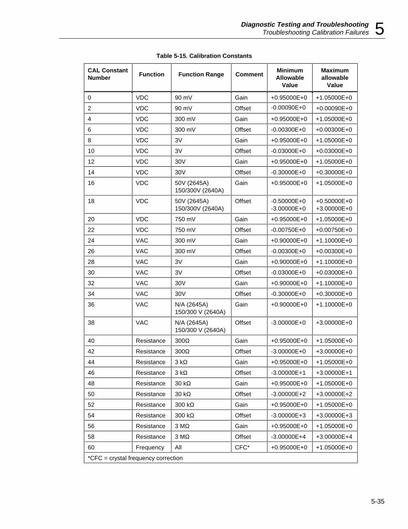
Diagnostic Testing and TroubleshootingTroubleshooting Calibration Failures 5
5-35
Table 5-15. Calibration Constants
CAL ConstantNumber Function Function Range Comment
MinimumAllowable
Value
Maximumallowable
Value
0 VDC 90 mV Gain +0.95000E+0 +1.05000E+0
2 VDC 90 mV Offset -0.00090E+0 +0.00090E+0
4 VDC 300 mV Gain +0.95000E+0 +1.05000E+0
6 VDC 300 mV Offset -0.00300E+0 +0.00300E+0
8 VDC 3V Gain +0.95000E+0 +1.05000E+0
10 VDC 3V Offset -0.03000E+0 +0.03000E+0
12 VDC 30V Gain +0.95000E+0 +1.05000E+0
14 VDC 30V Offset -0.30000E+0 +0.30000E+0
16 VDC 50V (2645A)150/300V (2640A)
Gain +0.95000E+0 +1.05000E+0
18 VDC 50V (2645A)150/300V (2640A)
Offset -0.50000E+0-3.00000E+0
+0.50000E+0+3.00000E+0
20 VDC 750 mV Gain +0.95000E+0 +1.05000E+0
22 VDC 750 mV Offset -0.00750E+0 +0.00750E+0
24 VAC 300 mV Gain +0.90000E+0 +1.10000E+0
26 VAC 300 mV Offset -0.00300E+0 +0.00300E+0
28 VAC 3V Gain +0.90000E+0 +1.10000E+0
30 VAC 3V Offset -0.03000E+0 +0.03000E+0
32 VAC 30V Gain +0.90000E+0 +1.10000E+0
34 VAC 30V Offset -0.30000E+0 +0.30000E+0
36 VAC N/A (2645A)150/300 V (2640A)
Gain +0.90000E+0 +1.10000E+0
38 VAC N/A (2645A)150/300 V (2640A)
Offset -3.00000E+0 +3.00000E+0
40 Resistance 300Ω Gain +0.95000E+0 +1.05000E+0
42 Resistance 300Ω Offset -3.00000E+0 +3.00000E+0
44 Resistance 3 kΩ Gain +0.95000E+0 +1.05000E+0
46 Resistance 3 kΩ Offset -3.00000E+1 +3.00000E+1
48 Resistance 30 kΩ Gain +0.95000E+0 +1.05000E+0
50 Resistance 30 kΩ Offset -3.00000E+2 +3.00000E+2
52 Resistance 300 kΩ Gain +0.95000E+0 +1.05000E+0
54 Resistance 300 kΩ Offset -3.00000E+3 +3.00000E+3
56 Resistance 3 MΩ Gain +0.95000E+0 +1.05000E+0
58 Resistance 3 MΩ Offset -3.00000E+4 +3.00000E+4
60 Frequency All CFC* +0.95000E+0 +1.05000E+0
*CFC = crystal frequency correction
NetDAQService Manual
5-36
The frequency counter calibration constant is simply the Gain constant calculation wherethe lowTarget and lowMeas are both assumed to be zero.
FrequencyConstant = targetFreq / measFreq
To retrieve the calibration constants, set up the instrument in the manual calibrationconfiguration described in “Calibration Procedure (Manual)“ in Chapter 4. Then retrievethe desired calibration constant with the CAL_CONST? xx command, where xx denotesthe calibration constant number shown in Table 5-15. Each constant reflects thecorrection applied to the uncompensated measurement result as an offset or as a gainmultiplier. For example, CAL_CONST? 8 might return +998.939E-3 indicating theuncompensated value for the 3V dc range is multiplied by 0.998939 to achievespecification.
Loading Embedded Instrument Firmware 5-38.Instrument firmware consists of the following components:
Main Firmware Loaded from a floppy disk on the PC to the instrument via theinstrument rear panel RS-232 port. This is a closed-case procedure and it is notnecessary to open the instrument to load the Main Firmware. The Main Firmware isidentical for both model instruments.
A/D Firmware Loaded from a floppy disk on the PC to the instrument directly to a3-pin connection on the A3 A/D Converter PCA. This also requires a separate powersupply connection to the A3 A/D Converter PCA Flash Memory, and custom cables formaking the connections. This is not a closed-case procedure and it is necessary to openthe instrument to load the A/D Firmware. The A/D Firmware is different for eachinstrument.
Firmware is stored in the instrument in electrically erasable and programmable memorydevices. A diskette containing the necessary loading software and latest release of thefirmware may be obtained from either your local Fluke authorized service center, orfrom the Fluke factory. You may also contact the factory directly: Fluke DataAcquisition Sales Support, (206) 356-5870 or FAX, (206) 356-5790.
To review which versions of the Main and A/D firmware are presently in yourinstrument, see “Diagnostic Tool idS” earlier in this chapter. The listing for A/DFirmware is identified as AtodM; the listing for Main Firmware is identified as Main.The remaining firmware for the display, FPGA and so forth are factory procedures only.
Firmware Diskette 5-39.
The firmware diskette contains the files shown in Table 5-16. The *.bat files are used forthe standard installation of the firmware. If you wish to customize the installation, then donot run the batch file, but refer to Table 5-16 for the switches used for the executable fileld26xx.exe. Create a directory on your hard drive for this diskette and then copy thecontents to the hard drive. For example, create the directory on your hard drive calledfirmware and copy the contents of the diskette into this directory. (Refer to yourWindows or DOS documentation if you need information on creating directories orcopying files.)
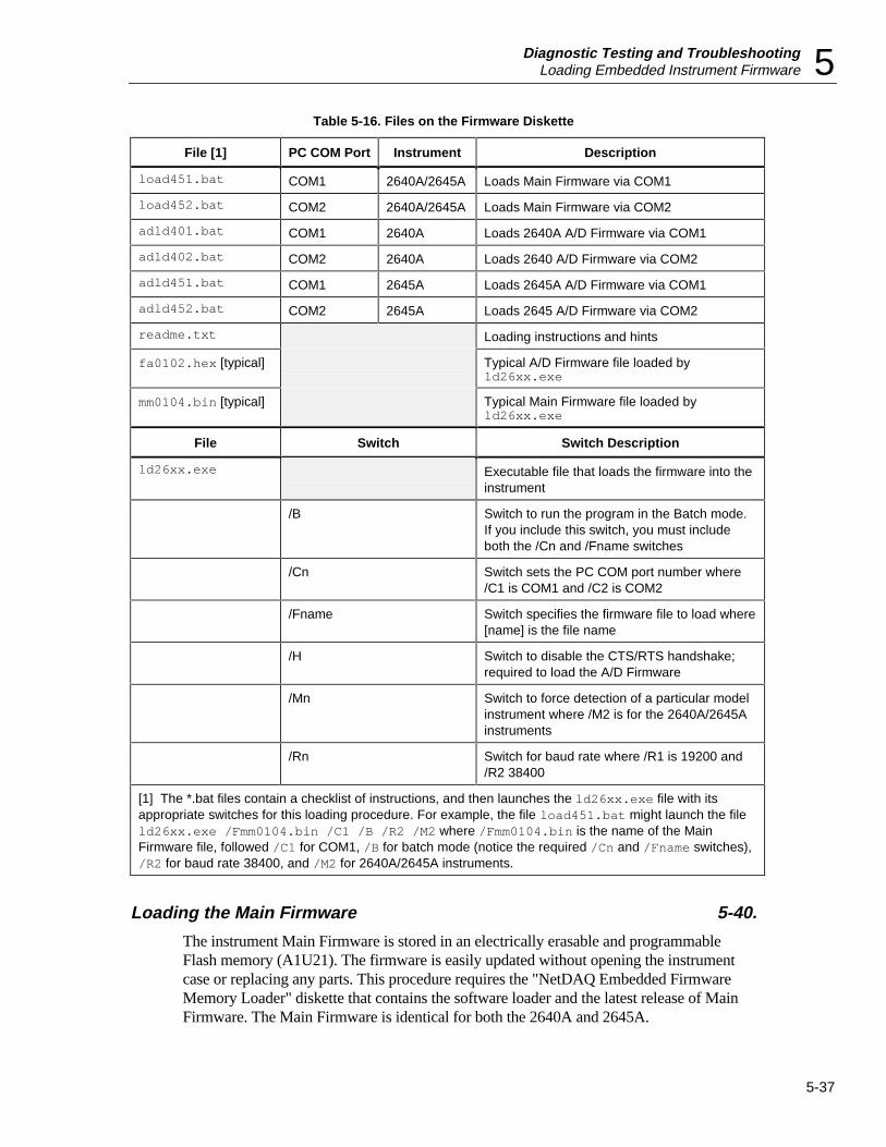
Diagnostic Testing and TroubleshootingLoading Embedded Instrument Firmware 5
5-37
Table 5-16. Files on the Firmware Diskette
File [1] PC COM Port Instrument Description
load451.bat COM1 2640A/2645A Loads Main Firmware via COM1
load452.bat COM2 2640A/2645A Loads Main Firmware via COM2
adld401.bat COM1 2640A Loads 2640A A/D Firmware via COM1
adld402.bat COM2 2640A Loads 2640 A/D Firmware via COM2
adld451.bat COM1 2645A Loads 2645A A/D Firmware via COM1
adld452.bat COM2 2645A Loads 2645 A/D Firmware via COM2
readme.txt Loading instructions and hints
fa0102.hex [typical] Typical A/D Firmware file loaded byld26xx.exe
mm0104.bin [typical] Typical Main Firmware file loaded byld26xx.exe
File Switch Switch Description
ld26xx.exe Executable file that loads the firmware into theinstrument
/B Switch to run the program in the Batch mode.If you include this switch, you must includeboth the /Cn and /Fname switches
/Cn Switch sets the PC COM port number where/C1 is COM1 and /C2 is COM2
/Fname Switch specifies the firmware file to load where[name] is the file name
/H Switch to disable the CTS/RTS handshake;required to load the A/D Firmware
/Mn Switch to force detection of a particular modelinstrument where /M2 is for the 2640A/2645Ainstruments
/Rn Switch for baud rate where /R1 is 19200 and/R2 38400
[1] The *.bat files contain a checklist of instructions, and then launches the ld26xx.exe file with itsappropriate switches for this loading procedure. For example, the file load451.bat might launch the fileld26xx.exe /Fmm0104.bin /C1 /B /R2 /M2 where /Fmm0104.bin is the name of the MainFirmware file, followed /C1 for COM1, /B for batch mode (notice the required /Cn and /Fname switches),/R2 for baud rate 38400, and /M2 for 2640A/2645A instruments.
Loading the Main Firmware 5-40.
The instrument Main Firmware is stored in an electrically erasable and programmableFlash memory (A1U21). The firmware is easily updated without opening the instrumentcase or replacing any parts. This procedure requires the "NetDAQ Embedded FirmwareMemory Loader" diskette that contains the software loader and the latest release of MainFirmware. The Main Firmware is identical for both the 2640A and 2645A.
NetDAQService Manual
5-38
Complete the following procedure to load the Main Firmware. Use this procedure only ifthe normal defaults specified for the *.bat file are acceptable. If you want to customizethis installation, refer to Table 5-16.
1. Set up the instrument for RS-232 communications as described in “CalibrationProcedure (Manual)“ in Chapter 4, only use a baud rate of 38400 instead of 19200.Note which PC COM port was used for the RS-232 connection.
2. At the PC, obtain the DOS prompt C:\>. (Do not shell to the DOS prompt fromWindows.)
3. If you have not already done so, copy the contents of the diskette into a directory onyour hard drive, e.g., firmware, and change to this directory (C:\firmware>).
4. After the DOS prompt in the directory with the diskette files, type load451.bat ifyou connected to PC COM port 1, or load452.bat if you connected to PC COMport 2. For example, type the command C:\firmware>load451.bat; then press<Enter>.
5. Observe the checklist for this installation, a pause (press <Cntl><C> to escape at thispoint), and then press any key to the launch the executable ld26xx.exe with itsappropriate switches for this loading application (see Table 5-16).
6. While loading; the instrument display shows “boot.” Allow several minutes for thefirmware loading process to complete. The PC screen will show Loading Line as thefirmware is loaded. Do not interrupt this process by touching the PC keyboard orremoving power from the instrument. After the completion of the firmware, the screenshows Done Loading and the DOS prompt is returned.
7. To confirm the successful loading of the new firmware, see “Diagnostic Tool idS”earlier in this chapter and note the new version of the Main Firmware identified asMain.
Loading the A/D Firmware 5-41.
The instrument A/D Firmware is stored in an electrically erasable and programmable Flashmemory (A3U6). The Program Power for A3U6 is from an external source at A3P2 (orA3J3) and the firmware loads from an internal connection at A3P1. This means you mustremove the case to load the A/D firmware. The A/D Firmware is specific to the 2640A or2645A. Be sure you are loading the correct program.
Complete the following procedure to load the A/D Firmware. Use this procedure only if thenormal defaults specified for the *.bat file are acceptable. If you want to customize thisinstallation, refer to Table 5-16.
1. Remove the instrument case as described in the procedure “Removing theInstrument Case” in Chapter 3.
2. Locate contacts for A3W5 and install a jumper across these contacts. This connectsVcc to the line VBOOT (for the A3U5 microprocessor) and prevents A3U5 frominitializing the A3 A/D Converter PCA kernel.
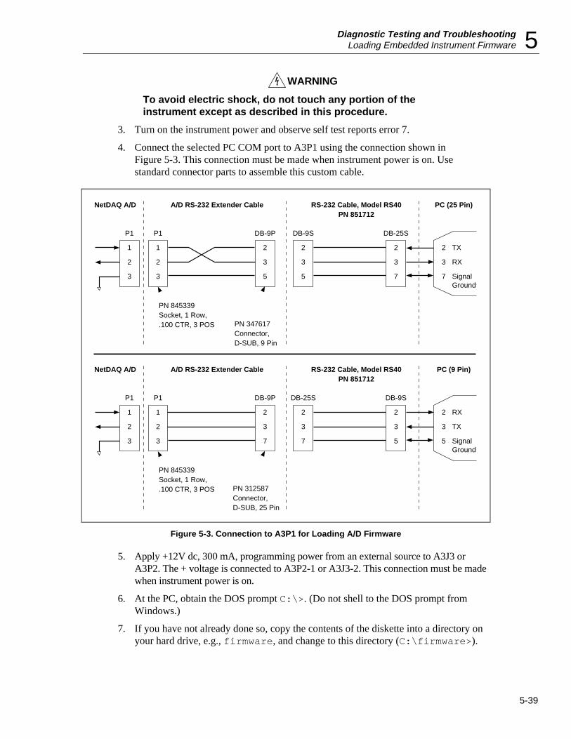
Diagnostic Testing and TroubleshootingLoading Embedded Instrument Firmware 5
5-39
WARNING
To avoid electric shock, do not touch any portion of theinstrument except as described in this procedure.
3. Turn on the instrument power and observe self test reports error 7.
4. Connect the selected PC COM port to A3P1 using the connection shown inFigure 5-3. This connection must be made when instrument power is on. Usestandard connector parts to assemble this custom cable.
P1
1
2
3
P1
1
2
3
DB-9S
2
3
5
DB-9P
2
3
5
2
3
7
DB-25S
2
3
7
PC (25 Pin)
TX
RX
SignalGround
PN 845339Socket, 1 Row, .100 CTR, 3 POS PN 347617
Connector, D-SUB, 9 Pin
RS-232 Cable, Model RS40PN 851712
A/D RS-232 Extender CableNetDAQ A/D
P1
1
2
3
P1
1
2
3
DB-25S
2
3
7
DB-9P
2
3
7
2
3
5
DB-9S
2
3
5
PC (9 Pin)
RX
TX
SignalGround
PN 845339Socket, 1 Row, .100 CTR, 3 POS PN 312587
Connector, D-SUB, 25 Pin
RS-232 Cable, Model RS40PN 851712
A/D RS-232 Extender CableNetDAQ A/D
Figure 5-3. Connection to A3P1 for Loading A/D Firmware
5. Apply +12V dc, 300 mA, programming power from an external source to A3J3 orA3P2. The + voltage is connected to A3P2-1 or A3J3-2. This connection must be madewhen instrument power is on.
6. At the PC, obtain the DOS prompt C:\>. (Do not shell to the DOS prompt fromWindows.)
7. If you have not already done so, copy the contents of the diskette into a directory onyour hard drive, e.g., firmware, and change to this directory (C:\firmware>).
NetDAQService Manual
5-40
8. 2640A After the DOS prompt in the directory with the diskette files, typeadld401.bat if you connected to PC COM port 1, or adld402.bat if youconnected to PC COM port 2. For example, type the commandC:\firmware>adld401.bat; then press <Enter>.
-or-
2645A After the DOS prompt in the directory with the diskette files, typeadld451.bat if you connected to PC COM port 1, or adld452.bat if youconnected to PC COM port 2. For example, type the commandC:\firmware>adld451.bat; then press <Enter>.
9. Observe the checklist for this installation, a pause (press <Cntl><C> to escape at thispoint), and then press any key to the launch the executable ld26xx.exe with itsappropriate switches for this loading application (see Table 5-16).
10. Allow several minutes for the firmware loading process to complete. The PC screenwill show Loading Line as the firmware is loaded. Do not interrupt this process bytouching the PC keyboard or removing power from the instrument. After thecompletion of the firmware, the screen shows Done Loading and the DOS prompt isreturned.
11. With the instrument power still on, remove the +12V dc connection at A3J3 or A3P2.
12. Turn the instrument power off and remove the connection at A3P1.
13. IMPORTANT! Remove the jumper at A3W5.
14. Reinstall the instrument case using the procedure “Installing the Instrument Case” inChapter 3.
15. Turn on the instrument power and verify you do not receive self-test error code 7,which would indicate you failed to remove the A3W5 jumper in Step 13.
16. To confirm the successful loading of the new firmware, see “Diagnostic Tool idS”earlier in this chapter and note the new version of the A/D Firmware identified asAtodM.
6-1
Chapter 6List of Replaceable Parts
Title Page
6-1. Introduction ............................................................................................ 6-36-2. How To Obtain Parts.............................................................................. 6-36-3. Manual Status Information..................................................................... 6-36-4. Newer Instruments ................................................................................. 6-46-5. Service Centers....................................................................................... 6-4

NetDAQService Manual
6-2
List of Replaceable PartsIntroduction 6
6-3
Introduction 6-1.This chapter contains an illustrated list of replaceable parts for models 2640A and2645A Data Acquisition Units. Parts are listed by assembly; alphabetized by referencedesignator. Each assembly is accompanied by an illustration showing the location ofeach part and its reference designator. The parts lists give the following information:
• Reference designator (for example, “R52”).• An indication if the part is subject to damage by static discharge.• Description.• Fluke stock number.• Total quantity.• Any special notes (i.e., factory-selected part).
CAUTION
A * symbol indicates a device that may be damaged by staticdischarge.
How To Obtain Parts 6-2.Electronic components may be ordered directly from the Fluke Corporation and itsauthorized representatives by using the part number under the heading FLUKE STOCKNO. In the U.S., order directly from the Fluke Parts Dept. by calling 1-800-526-4731.Parts price information is available from the Fluke Corporation or its representatives.
In the event that the part ordered has been replaced by a new or improved part, thereplacement will be accompanied by an explanatory note and installation instructions, ifnecessary.
To ensure prompt delivery of the correct part, include the following information whenyou place an order:
• Instrument model and serial number.• Part number and revision level of the pca (printed circuit assembly) containing the
part.• Reference designator.• Fluke stock number.• Description (as given under the DESCRIPTION heading).• Quantity.
Manual Status Information 6-3.The Manual Status Information table that precedes the parts list defines the assemblyrevision levels that are documented in the manual. Revision levels are printed on thecomponent side of each pca.
NetDAQService Manual
6-4
Newer Instruments 6-4.Changes and improvements made to the instrument are identified by incrementing therevision letter marked on the affected pca. These changes are documented on asupplemental change/errata sheet which, when applicable, is included with the manual.
Service Centers 6-5.A list of service centers that may be contacted for any items on the Parts Lists is locatedat the end of this chapter.
NOTE
This instrument may contain a Nickel-Cadmium battery. Do not mix withthe solid waste stream. Spent batteries should be disposed of by a qualifiedrecycler or hazardous materials handler. Contact your authorized Flukeservice center for recycling information.
WARNING
THIS INSTRUMENT CONTAINS A FUSIBLE RESISTOR (PN650085). TO ENSURE SAFETY, USE EXACT REPLACMENTONLY.
MANUAL STATUS INFORMATION
Ref or Option number Assembly name Fluke Part Number Revision Level
A1 Main PCA 938089 D
A2 Display PCA 814194 –
A3 2640A A/D Converter PCA 938100 C
A3 2645A A/D Converter PCA 932652 C
A4 Analog Input PCA 814210 C
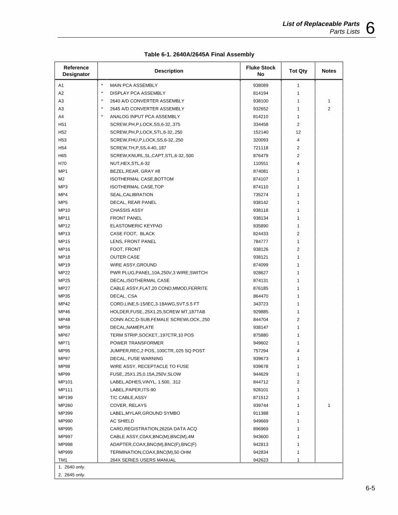
List of Replaceable PartsParts Lists 6
6-5
Table 6-1. 2640A/2645A Final Assembly
ReferenceDesignator
DescriptionFluke Stock
NoTot Qty Notes
A1 * MAIN PCA ASSEMBLY 938089 1
A2 * DISPLAY PCA ASSEMBLY 814194 1
A3 * 2640 A/D CONVERTER ASSEMBLY 938100 1 1
A3 * 2645 A/D CONVERTER ASSEMBLY 932652 1 2
A4 * ANALOG INPUT PCA ASSEMBLY 814210 1
H51 SCREW,PH,P,LOCK,SS,6-32,.375 334458 2
H52 SCREW,PH,P,LOCK,STL,6-32,.250 152140 12
H53 SCREW,FHU,P,LOCK,SS,6-32,.250 320093 4
H54 SCREW,TH,P,SS,4-40,.187 721118 2
H65 SCREW,KNURL,SL,CAPT,STL,6-32,.500 876479 2
H70 NUT,HEX,STL,6-32 110551 4
MP1 BEZEL,REAR, GRAY #8 874081 1
M2 ISOTHERMAL CASE,BOTTOM 874107 1
MP3 ISOTHERMAL CASE,TOP 874110 1
MP4 SEAL,CALIBRATION 735274 1
MP5 DECAL, REAR PANEL 938142 1
MP10 CHASSIS ASSY 938118 1
MP11 FRONT PANEL 938134 1
MP12 ELASTOMERIC KEYPAD 935890 1
MP13 CASE FOOT, BLACK 824433 2
MP15 LENS, FRONT PANEL 784777 1
MP16 FOOT, FRONT 938126 2
MP18 OUTER CASE 938121 1
MP19 WIRE ASSY,GROUND 874099 1
MP22 PWR PLUG,PANEL,10A,250V,3 WIRE,SWITCH 928627 1
MP25 DECAL,ISOTHERMAL CASE 874131 1
MP27 CABLE ASSY,FLAT,20 COND,MMOD,FERRITE 876185 1
MP35 DECAL, CSA 864470 1
MP42 CORD,LINE,5-15/IEC,3-18AWG,SVT,5.5 FT 343723 1
MP46 HOLDER,FUSE,.25X1.25,SCREW MT,187TAB 929885 1
MP48 CONN ACC,D-SUB,FEMALE SCREWLOCK,.250 844704 2
MP59 DECAL,NAMEPLATE 938147 1
MP67 TERM STRIP,SOCKET,.197CTR,10 POS 875880 1
MP71 POWER TRANSFORMER 949602 1
MP95 JUMPER,REC,2 POS,.100CTR,.025 SQ POST 757294 4
MP97 DECAL, FUSE WARNING 939673 1
MP98 WIRE ASSY, RECEPTACLE TO FUSE 939678 1
MP99 FUSE,.25X1.25,0.15A,250V,SLOW 944629 1
MP101 LABEL,ADHES,VINYL, 1.500, .312 844712 2
MP111 LABEL,PAPER,ITS-90 928101 1
MP199 T/C CABLE,ASSY 871512 1
MP260 COVER, RELAYS 939744 1 1
MP399 LABEL,MYLAR,GROUND SYMBO 911388 1
MP990 AC SHIELD 949669 1
MP995 CARD,REGISTRATION,2620A DATA ACQ 896969 1
MP997 CABLE ASSY,C0AX,BNC(M),BNC(M),4M 943600 1
MP998 ADAPTER,COAX,BNC(M),BNC(F),BNC(F) 942813 1
MP999 TERMINATION,COAX,BNC(M),50 OHM 942834 1
TM1 264X SERIES USERS MANUAL 942623 1
1. 2640 only.
2. 2645 only.
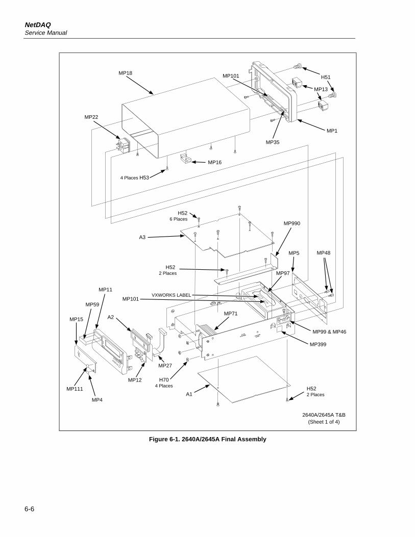
NetDAQService Manual
6-6
A3
H52 2 Places
A1H522 Places
H704 Places
A2
H526 Places
MP990
MP48
MP12
MP15
MP11
MP111
MP4
MP27
MP71
MP399
MP99 & MP46
MP5
MP1
H51
MP13
MP101
MP35
MP18
MP22
4 Places H53
VXWORKS LABELMP101
MP97
2640A/2645A T&B(Sheet 1 of 4)
MP16
MP59
Figure 6-1. 2640A/2645A Final Assembly
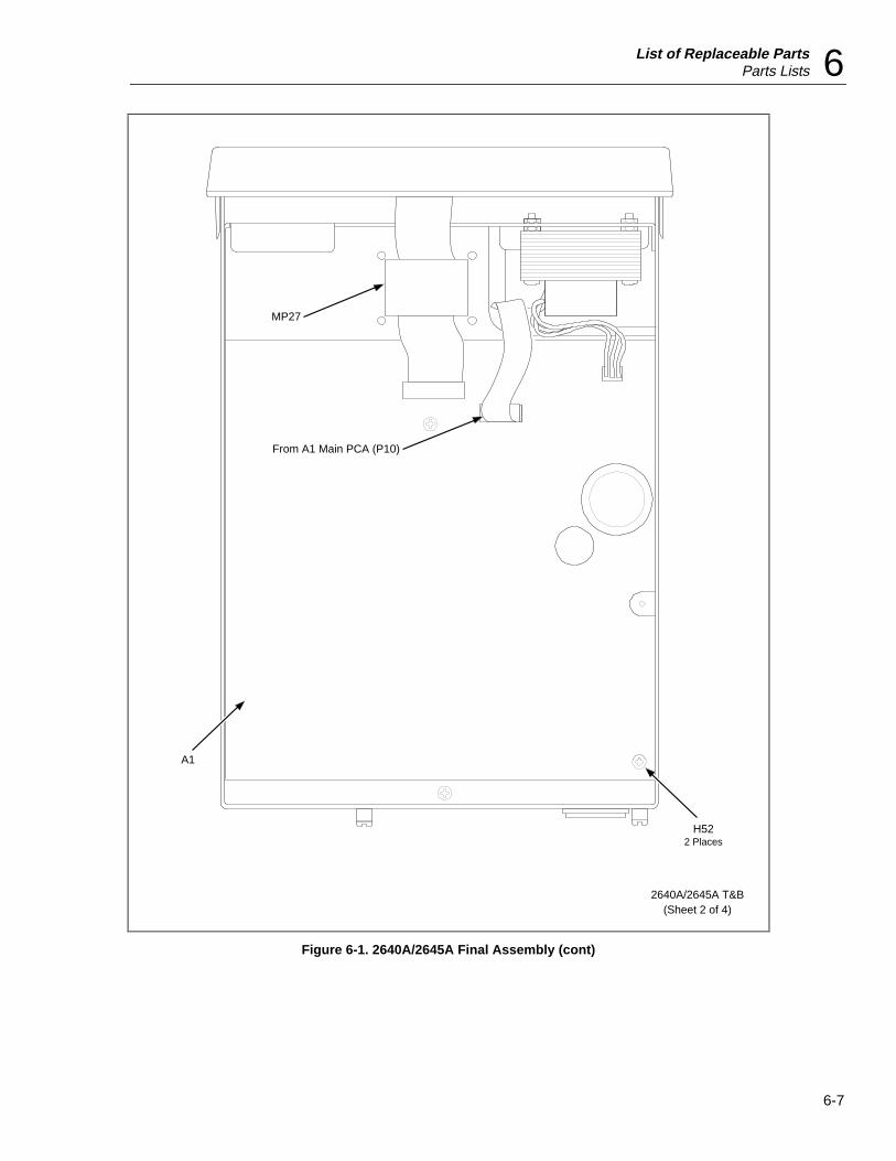
List of Replaceable PartsParts Lists 6
6-7
MP27
From A1 Main PCA (P10)
H522 Places
A1
2640A/2645A T&B(Sheet 2 of 4)
Figure 6-1. 2640A/2645A Final Assembly (cont)
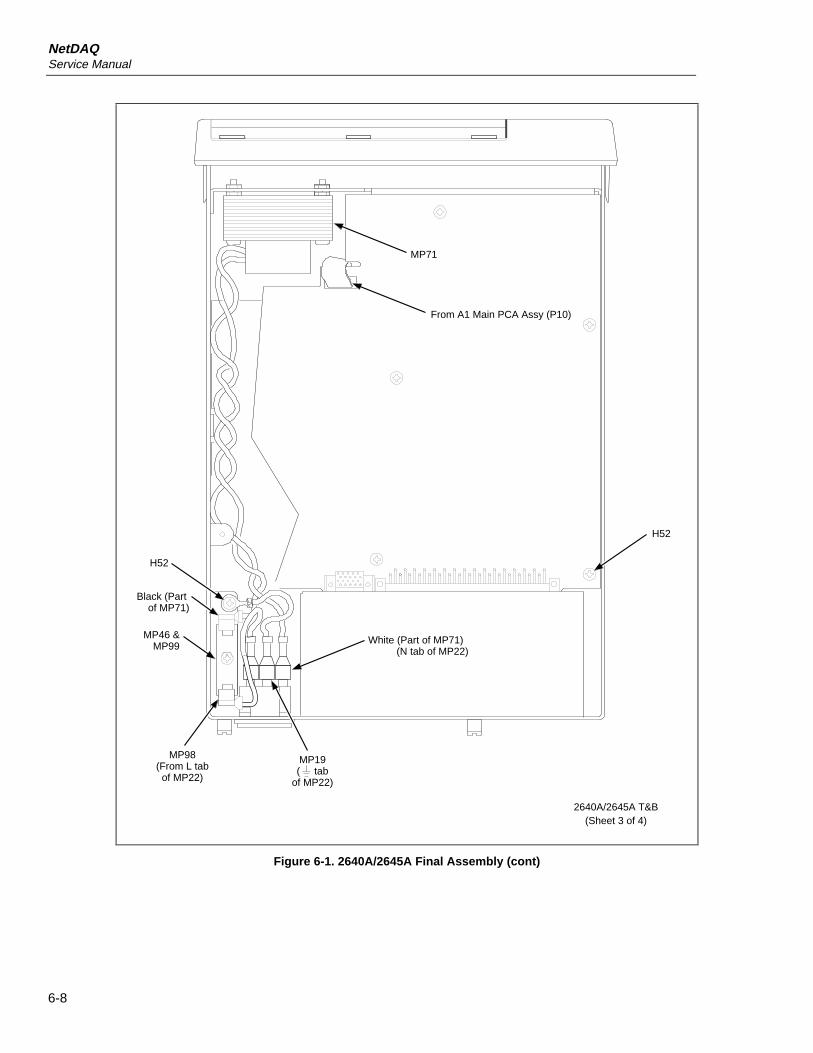
NetDAQService Manual
6-8
White (Part of MP71) (N tab of MP22)
H52
Black (Part of MP71)
MP46 &MP99
MP98(From L tabof MP22)
MP19( tab
of MP22)
H52
MP71
From A1 Main PCA Assy (P10)
2640A/2645A T&B(Sheet 3 of 4)
Figure 6-1. 2640A/2645A Final Assembly (cont)
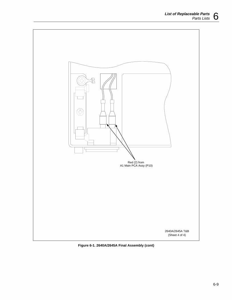
List of Replaceable PartsParts Lists 6
6-9
Red (2) from A1 Main PCA Assy (P10)
2640A/2645A T&B(Sheet 4 of 4)
Figure 6-1. 2640A/2645A Final Assembly (cont)
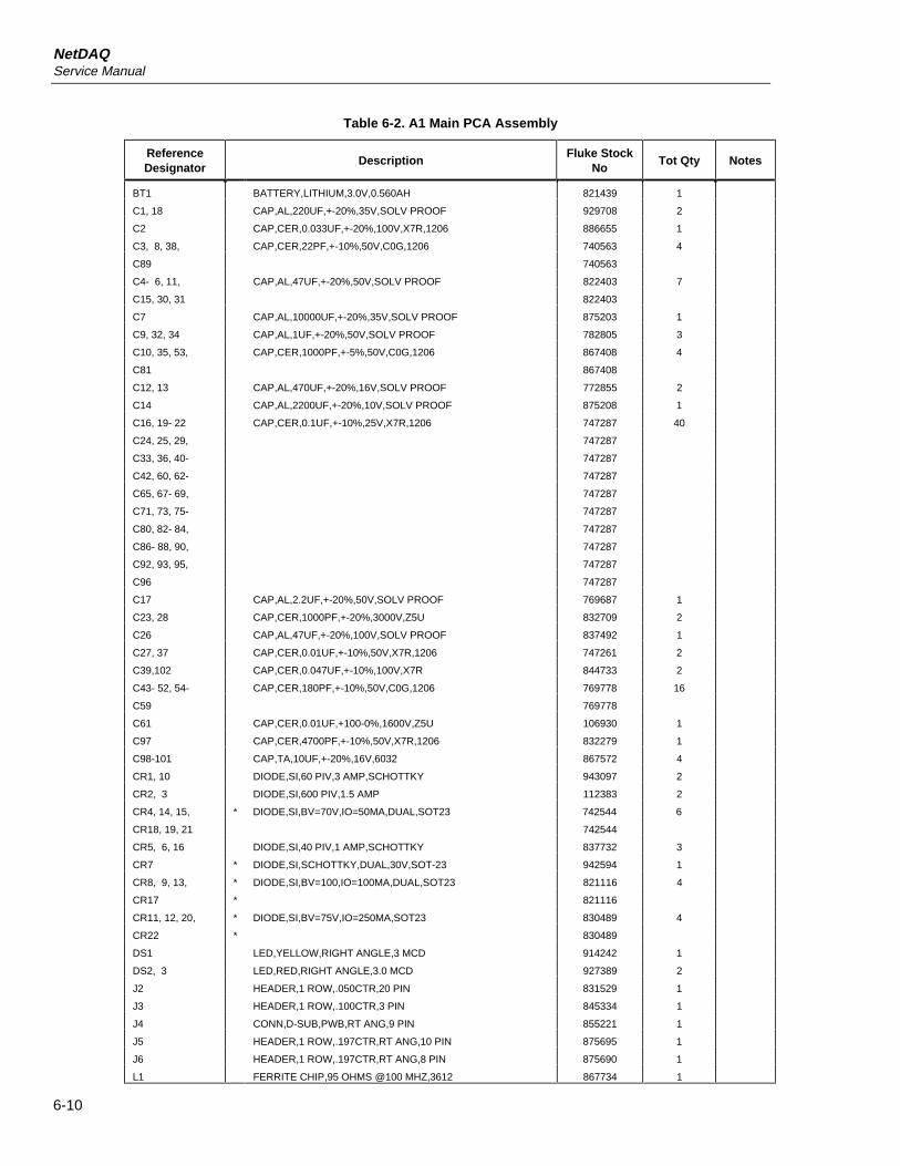
NetDAQService Manual
6-10
Table 6-2. A1 Main PCA Assembly
ReferenceDesignator
DescriptionFluke Stock
NoTot Qty Notes
BT1 BATTERY,LITHIUM,3.0V,0.560AH 821439 1
C1, 18 CAP,AL,220UF,+-20%,35V,SOLV PROOF 929708 2
C2 CAP,CER,0.033UF,+-20%,100V,X7R,1206 886655 1
C3, 8, 38, CAP,CER,22PF,+-10%,50V,C0G,1206 740563 4
C89 740563
C4- 6, 11, CAP,AL,47UF,+-20%,50V,SOLV PROOF 822403 7
C15, 30, 31 822403
C7 CAP,AL,10000UF,+-20%,35V,SOLV PROOF 875203 1
C9, 32, 34 CAP,AL,1UF,+-20%,50V,SOLV PROOF 782805 3
C10, 35, 53, CAP,CER,1000PF,+-5%,50V,C0G,1206 867408 4
C81 867408
C12, 13 CAP,AL,470UF,+-20%,16V,SOLV PROOF 772855 2
C14 CAP,AL,2200UF,+-20%,10V,SOLV PROOF 875208 1
C16, 19- 22 CAP,CER,0.1UF,+-10%,25V,X7R,1206 747287 40
C24, 25, 29, 747287
C33, 36, 40- 747287
C42, 60, 62- 747287
C65, 67- 69, 747287
C71, 73, 75- 747287
C80, 82- 84, 747287
C86- 88, 90, 747287
C92, 93, 95, 747287
C96 747287
C17 CAP,AL,2.2UF,+-20%,50V,SOLV PROOF 769687 1
C23, 28 CAP,CER,1000PF,+-20%,3000V,Z5U 832709 2
C26 CAP,AL,47UF,+-20%,100V,SOLV PROOF 837492 1
C27, 37 CAP,CER,0.01UF,+-10%,50V,X7R,1206 747261 2
C39,102 CAP,CER,0.047UF,+-10%,100V,X7R 844733 2
C43- 52, 54- CAP,CER,180PF,+-10%,50V,C0G,1206 769778 16
C59 769778
C61 CAP,CER,0.01UF,+100-0%,1600V,Z5U 106930 1
C97 CAP,CER,4700PF,+-10%,50V,X7R,1206 832279 1
C98-101 CAP,TA,10UF,+-20%,16V,6032 867572 4
CR1, 10 DIODE,SI,60 PIV,3 AMP,SCHOTTKY 943097 2
CR2, 3 DIODE,SI,600 PIV,1.5 AMP 112383 2
CR4, 14, 15, * DIODE,SI,BV=70V,IO=50MA,DUAL,SOT23 742544 6
CR18, 19, 21 742544
CR5, 6, 16 DIODE,SI,40 PIV,1 AMP,SCHOTTKY 837732 3
CR7 * DIODE,SI,SCHOTTKY,DUAL,30V,SOT-23 942594 1
CR8, 9, 13, * DIODE,SI,BV=100,IO=100MA,DUAL,SOT23 821116 4
CR17 * 821116
CR11, 12, 20, * DIODE,SI,BV=75V,IO=250MA,SOT23 830489 4
CR22 * 830489
DS1 LED,YELLOW,RIGHT ANGLE,3 MCD 914242 1
DS2, 3 LED,RED,RIGHT ANGLE,3.0 MCD 927389 2
J2 HEADER,1 ROW,.050CTR,20 PIN 831529 1
J3 HEADER,1 ROW,.100CTR,3 PIN 845334 1
J4 CONN,D-SUB,PWB,RT ANG,9 PIN 855221 1
J5 HEADER,1 ROW,.197CTR,RT ANG,10 PIN 875695 1
J6 HEADER,1 ROW,.197CTR,RT ANG,8 PIN 875690 1
L1 FERRITE CHIP,95 OHMS @100 MHZ,3612 867734 1
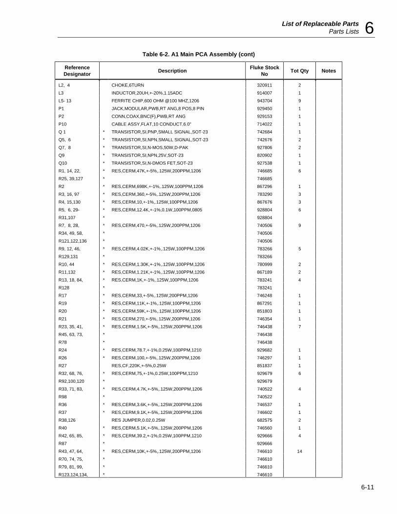
List of Replaceable PartsParts Lists 6
6-11
Table 6-2. A1 Main PCA Assembly (cont)
ReferenceDesignator
DescriptionFluke Stock
NoTot Qty Notes
L2, 4 CHOKE,6TURN 320911 2
L3 INDUCTOR,20UH,+-20%,1.15ADC 914007 1
L5- 13 FERRITE CHIP,600 OHM @100 MHZ,1206 943704 9
P1 JACK,MODULAR,PWB,RT ANG,8 POS,8 PIN 929450 1
P2 CONN,COAX,BNC(F),PWB,RT ANG 929153 1
P10 CABLE ASSY,FLAT,10 CONDUCT,6.0" 714022 1
Q 1 * TRANSISTOR,SI,PNP,SMALL SIGNAL,SOT-23 742684 1
Q5, 6 * TRANSISTOR,SI,NPN,SMALL SIGNAL,SOT-23 742676 2
Q7, 8 * TRANSISTOR,SI,N-MOS,50W,D-PAK 927806 2
Q9 * TRANSISTOR,SI,NPN,25V,SOT-23 820902 1
Q10 * TRANSISTOR,SI,N-DMOS FET,SOT-23 927538 1
R1, 14, 22, * RES,CERM,47K,+-5%,.125W,200PPM,1206 746685 6
R25, 39,127 * 746685
R2 * RES,CERM,698K,+-1%,.125W,100PPM,1206 867296 1
R3, 16, 97 * RES,CERM,360,+-5%,.125W,200PPM,1206 783290 3
R4, 15,130 * RES,CERM,10,+-1%,.125W,100PPM,1206 867676 3
R5, 6, 29- * RES,CERM,12.4K,+-1%,0.1W,100PPM,0805 928804 6
R31,107 * 928804
R7, 8, 28, * RES,CERM,470,+-5%,.125W,200PPM,1206 740506 9
R34, 49, 58, * 740506
R121,122,136 * 740506
R9, 12, 46, * RES,CERM,4.02K,+-1%,.125W,100PPM,1206 783266 5
R129,131 * 783266
R10, 44 * RES,CERM,1.30K,+-1%,.125W,100PPM,1206 780999 2
R11,132 * RES,CERM,1.21K,+-1%,.125W,100PPM,1206 867189 2
R13, 18, 84, * RES,CERM,1K,+-1%,.125W,100PPM,1206 783241 4
R128 * 783241
R17 * RES,CERM,33,+-5%,.125W,200PPM,1206 746248 1
R19 * RES,CERM,11K,+-1%,.125W,100PPM,1206 867291 1
R20 * RES,CERM,59K,+-1%,.125W,100PPM,1206 851803 1
R21 * RES,CERM,270,+-5%,.125W,200PPM,1206 746354 1
R23, 35, 41, * RES,CERM,1.5K,+-5%,.125W,200PPM,1206 746438 7
R45, 63, 73, * 746438
R78 * 746438
R24 * RES,CERM,78.7,+-1%,0.25W,100PPM,1210 929682 1
R26 * RES,CERM,100,+-5%,.125W,200PPM,1206 746297 1
R27 RES,CF,220K,+-5%,0.25W 851837 1
R32, 68, 76, * RES,CERM,75,+-1%,0.25W,100PPM,1210 929679 6
R92,100,120 * 929679
R33, 71, 83, * RES,CERM,4.7K,+-5%,.125W,200PPM,1206 740522 4
R98 * 740522
R36 * RES,CERM,3.6K,+-5%,.125W,200PPM,1206 746537 1
R37 * RES,CERM,9.1K,+-5%,.125W,200PPM,1206 746602 1
R38,126 RES JUMPER,0.02,0.25W 682575 2
R40 * RES,CERM,5.1K,+-5%,.125W,200PPM,1206 746560 1
R42, 65, 85, * RES,CERM,39.2,+-1%,0.25W,100PPM,1210 929666 4
R87 * 929666
R43, 47, 64, * RES,CERM,10K,+-5%,.125W,200PPM,1206 746610 14
R70, 74, 75, * 746610
R79, 81, 99, * 746610
R123,124,134, * 746610
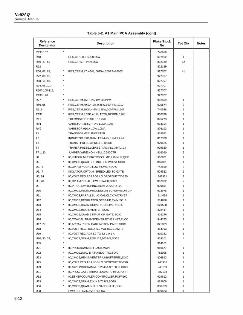
NetDAQService Manual
6-12
Table 6-2. A1 Main PCA Assembly (cont)
ReferenceDesignator
DescriptionFluke Stock
NoTot Qty Notes
R135,137 * 746610
R48 RES,CF,10K,+-5%,0.25W 697102 1
R50- 57, 59- RES,CF,47,+-5%,0.25W 822189 12
R62 822189
R66, 67, 69, * RES,CERM,47,+-5%,.0625W,200PPM,0603 927707 41
R72, 80, 82, * 927707
R88- 91, 93, * 927707
R94, 96,101- * 927707
R106,108-118, * 927707
R138-148 * 927707
R77 * RES,CERM,1M,+-5%,1W,200PPM 912589 1
R86, 95 * RES,CERM,49.9,+-1%,0.25W,100PPM,1210 929674 2
R119 * RES,CERM,100K,+-5%,.125W,200PPM,1206 740548 1
R133 * RES,CERM,3.32K,+-1%,.125W,100PPM,1206 810788 1
RT1 THERMISTOR,DISC,0.18,25C 875273 1
RV1 VARISTOR,41.5V,+-9%,1.0MA,1206 914114 1
RV2 VARISTOR,910,+-10%,1.0MA 876193 1
T1 TRANSFORMER, INVERTER 939681 1
T2 INDUCTOR,FXD,DUAL,EE24-25,0.4MH,1.2A 817379 1
T3 TRANSF,PULSE,3/PKG,1:1,100UH 929625 1
T4 TRANSF,PULSE,10BASE-T,RCV1:1,XMT1:1.4 929620 1
TP1, 30 JUMPER,WIRE,NONINSUL,0.200CTR 816090 2
U1 * IC,INTEGR MLTIPROTOCOL MPU,16 MHZ,QFP 910831 1
U2 * IC,CMOS,QUAD BUS BUFFER W/3-ST,SOIC 866801 1
U3, 4 * IC,OP AMP,QUAD,LOW POWER,SOIC 742569 2
U5, 7 * ISOLATOR,OPTO,HI-SPEED,LED TO GATE 504522 2
U6, 24 * IC,VOLT REG,ADJ,POS,LO DROPOUT,TO-220 943931 2
U8, 28 * IC,OP AMP,DUAL,LOW POWER,SOIC 867932 2
U9 * IC,V REG,SWITCHING,100KHZ,5A,TO-220 929591 1
U10 * IC,CMOS,MICROPROCESSOR SUPERVISOR,DIP 913975 1
U11 * IC,CMOS,PARALLEL I/O CAL/CLCK W/CRYST 914036 1
U12 * IC,CMOS,REGULATOR,STEP-UP,PWM,SO16 914080 1
U13 * IC,CMOS,RS232 DRIVER/RECEIVER,SOIC 821538 1
U14 * IC,CMOS,HEX INVERTER,SOIC 838417 1
U15 * IC,CMOS,QUAD 2 INPUT OR GATE,SOIC 838276 1
U16 * IC,COAXIAL TRANSCEIVER,ETHERNET,PLCC 944723 1
U17, 27 * IC,ARRAY,7 NPN DARLINGTON PAIRS,SOIC 821009 2
U18 * IC,VOLT REG,FIXED,-5.0 VOLTS,0.1 AMPS 454793 1
U19 * IC,VOLT REG,ADJ,1.2 TO 32 V,0.1 A 810242 1
U20, 30, 34, * IC,CMOS,SRAM,128K X 8,100 NS,SO32 914101 4
U35 * 914101
U21 * IC,PROGRAMMED FLASH,MAIN 949677 1
U22 * IC,CMOS,DUAL D F/F,+EDG TRG,SOIC 782995 1
U23 * IC,CMOS,HEX INVERTER,UNBUFFERED,SOIC 806893 1
U25 * IC,VOLT REG,ADJ,NEG,LO DROPOUT,TO-220 943936 1
U29 * IC,16V8,PROGRAMMED,2645A-90130,PLCC20 943159 1
U31 * IC,PROG GATE ARRAY,3000 G,70 MHZ,PQFP 887138 1
U32 * IC,ETHERCOUPLER CONTROLLER,PQFP160 929612 1
U33 * IC,CMOS,SRAM,32K X 8,70 NS,SO28 929609 1
U36 * IC,CMOS,QUAD INPUT NAND GATE,SOIC 830703 1
U38 PWR SUP,5VIN,9VOUT,1.8W 929583 1
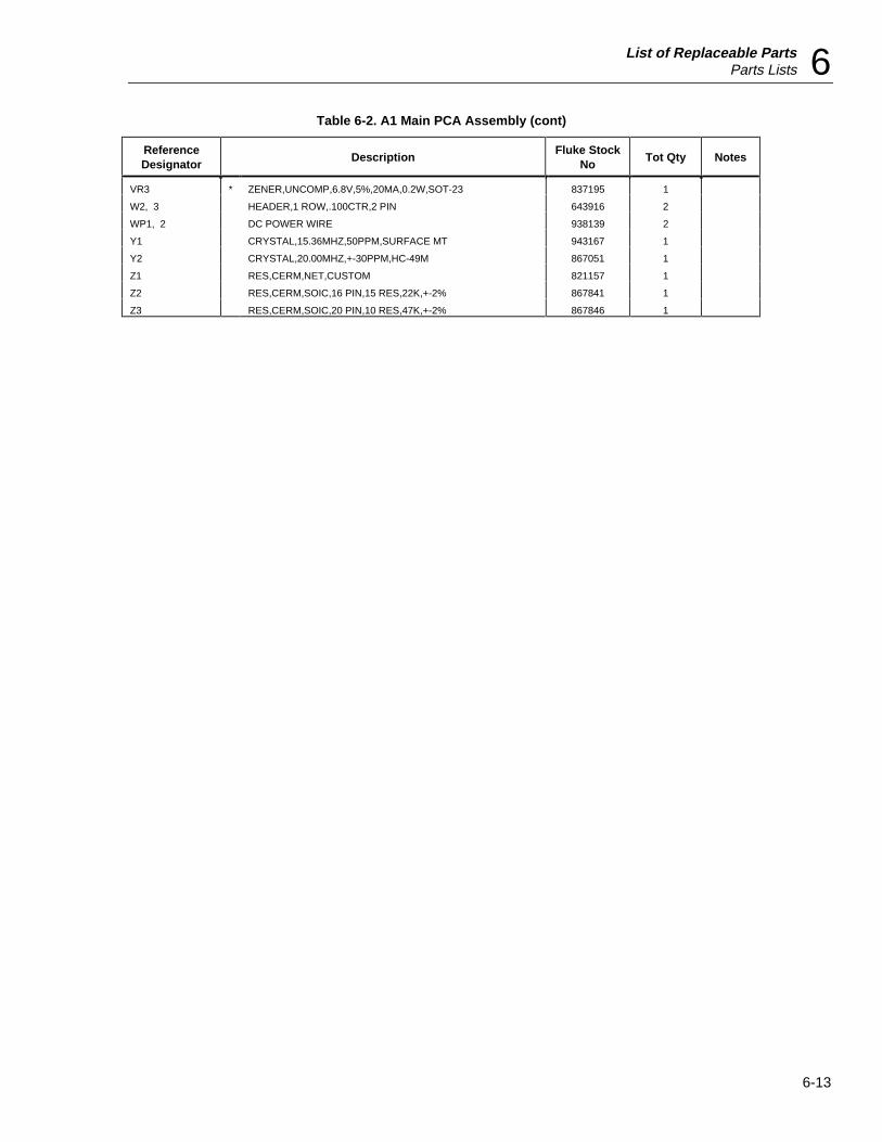
List of Replaceable PartsParts Lists 6
6-13
Table 6-2. A1 Main PCA Assembly (cont)
ReferenceDesignator
DescriptionFluke Stock
NoTot Qty Notes
VR3 * ZENER,UNCOMP,6.8V,5%,20MA,0.2W,SOT-23 837195 1
W2, 3 HEADER,1 ROW,.100CTR,2 PIN 643916 2
WP1, 2 DC POWER WIRE 938139 2
Y1 CRYSTAL,15.36MHZ,50PPM,SURFACE MT 943167 1
Y2 CRYSTAL,20.00MHZ,+-30PPM,HC-49M 867051 1
Z1 RES,CERM,NET,CUSTOM 821157 1
Z2 RES,CERM,SOIC,16 PIN,15 RES,22K,+-2% 867841 1
Z3 RES,CERM,SOIC,20 PIN,10 RES,47K,+-2% 867846 1
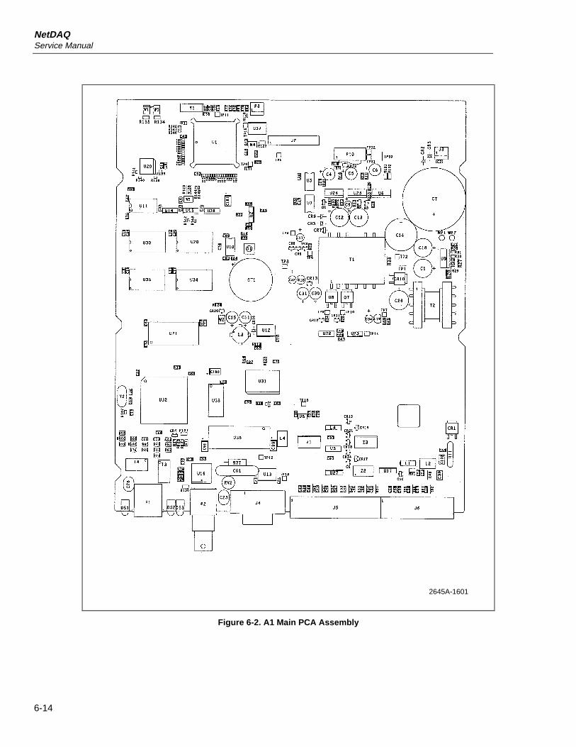
NetDAQService Manual
6-14
2645A-1601
Figure 6-2. A1 Main PCA Assembly
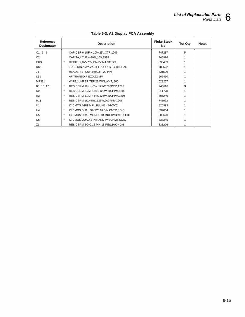
List of Replaceable PartsParts Lists 6
6-15
Table 6-3. A2 Display PCA Assembly
ReferenceDesignator
DescriptionFluke Stock
NoTot Qty Notes
C1, 3- 6 CAP,CER,0.1UF,+-10%,25V,X7R,1206 747287 5
C2 CAP,TA,4.7UF,+-20%,16V,3528 745976 1
CR3 * DIODE,SI,BV=75V,IO=250MA,SOT23 830489 1
DS1 TUBE,DISPLAY,VAC FLUOR,7 SEG,10 CHAR 783522 1
J1 HEADER,1 ROW,.050CTR,20 PIN 831529 1
LS1 AF TRANSD,PIEZO,22 MM 602490 1
MP321 WIRE,JUMPER,TEF,22AWG,WHT,.300 528257 1
R1, 10, 12 * RES,CERM,10K,+-5%,.125W,200PPM,1206 746610 3
R2 * RES,CERM,2.2M,+-5%,.125W,200PPM,1206 811778 1
R3 * RES,CERM,1.2M,+-5%,.125W,200PPM,1206 806240 1
R11 * RES,CERM,1K,+-5%,.125W,200PPM,1206 745992 1
U1 * IC,CMOS,4-BIT MPU,FLUKE 45-90002 820993 1
U4 * IC,CMOS,DUAL DIV BY 16 BIN CNTR,SOIC 837054 1
U5 * IC,CMOS,DUAL MONOSTB MULTIVBRTR,SOIC 806620 1
U6 * IC,CMOS,QUAD 2 IN NAND W/SCHMT,SOIC 837245 1
Z1 RES,CERM,SOIC,16 PIN,15 RES,10K,+-2% 836296 1
NetDAQService Manual
6-16
2620A-1601
Figure 6-3. A2 Display PCA Assembly
List of Replaceable PartsParts Lists 6
6-17
Table 6-4. 2640A A3 A/D Converter PCA Assembly
ReferenceDesignator
DescriptionFluke Stock
NoTot Qty Notes
C1- 4, 6- CAP,CER,0.1UF,+-10%,25V,X7R,1206 747287 60
C12, 16- 24, 747287
C28- 30, 32, 747287
C34, 36- 42, 747287
C47, 49- 55, 747287
C61- 63, 69, 747287
C70, 75, 77, 747287
C78, 81, 86- 747287
C96 747287
C5, 13- 15, CAP,TA,10UF,+-20%,16V,6032 867572 10
C31, 33, 45, 867572
C46, 67, 68 867572
C25, 48 CAP,CER,0.01UF,+-10%,50V,X7R,1206 747261 2
C26, 27 CAP,CER,27PF,+-10%,50V,C0G,1206 800508 2
C35, 56 CAP,CER,1000PF,+-10%,50V,C0G,1206 747378 2
C43 CAP,CER,3.3PF,+-0.5PF,50V,C0G,0805 514208 1
C44 CAP,POLYPR,1500PF,+-2.5%,100V 854641 1
C57- 59 CAP,POLYPR,0.1UF,+-10%,160V 446781 3
C60 CAP,POLYES,0.47UF,+-10%,50V 697409 1
C64, 65 CAP,AL,470UF,+-20%,10V,SOLV PROOF 822387 2
C66 CAP,POLYES,1UF,+-10%,50V 733089 1
C71, 72 CAP,TA,33UF,+-10%,6V 866897 2
C73 CAP,POLYPR,2200PF,+-5%,100V 854505 1
C74 CAP,CER,1000PF,+-5%,50V,C0G,1206 867408 1
C76 CAP,CER,4.3PF,+-0.5PF,50V,C0G,0805 514216 1
C79 CAP,CER,0.047UF,+-20%,50V,X7R,1206 782615 1
C80 CAP,POLYES,0.1UF,+-10%,1000V 837518 1
C82 CAP,CER,2500PF,+-20%,250V,X7R 485680 1
C83, 84 CAP,CER,15PF,+-10%,50V,C0G,1206 837393 2
C85 CAP,CER,68PF,+-2%,50V,C0G 715300 1
C97, 98 CAP,CER,180PF,+-2%,50V,C0G 820522 2
CR1- 6 * DIODE,SI,BV=70V,IO=50MA,DUAL,SOT23 742320 6
CR7, 21 * DIODE,SI,SCHOTTKY,DUAL,30V,SOT-23 942594 2
CR8- 14, 17- * DIODE,SI,DUAL,BV=50V,IO=100MA,SOT23 851659 10
CR19 * 851659
CR15 * DIODE,SI,BV=100,IO=100MA,DUAL,SOT23 821116 1
J1 CONN,DIN41612,TYPE C,RT ANG,48 PIN 867333 1
J2 CONN,MICRO-RIBBON,PLUG,RT ANG,20 POS 876107 1
J3 JACK,PWB,RT ANG,1.3MM PIN 943113 1
J10 HEADER,2 ROW,.100CTR,10 PIN 756858 1
K1- 20, 23, RELAY,REED,2 FORM A,5VDC,LOW THERM,HV 929711 22
K24 929711
K21, 22 RELAY,REED,2 FORM A,5VDC,LOWTHERM,1UV 944488 2
K25, 26 RELAY,ARMATURE,2 FORM C,5VDC,LATCH 836486 2
K27 RELAY,ARMATURE,4 FORM C,5V,LATCH 715078 1
L1- 49, 51 FERRITE CHIP,600 OHM @100 MHZ,1206 943704 50
L50, 53- 71 INDUCTOR,33UH,+-10%,0.115ADC 944509 20
L52 INDUCTOR,15MH,+-5%,0.021ADC 944251 1
MP200 INSUL PT,TRANSISTOR MOUNT,DAP,TO-5 152207 1
MP813,815 RIVET,S-TUB,OVAL,STL,.087,.343 838458 2
P1, 2 HEADER,1 ROW,.100CTR,3 PIN 845334 2
NetDAQService Manual
6-18
Table 6-4. 2640A A3 A/D Converter PCA Assembly (cont)
ReferenceDesignator
DescriptionFluke Stock
NoTot Qty Notes
Q1 * TRANSISTOR,SI,N-DMOS FET,SOT-23 927538 1
Q2, 4 * TRANSISTOR,SI,N-JFET,SOT-23 929588 2
Q3 * TRANSISTOR,SI,P-CHAN,SOT-23 832477 1
Q5 REF AMP SET 936047 1
Q6- 9, 19, * TRANSISTOR,SI,N-JFET,SOT-23 876263 10
Q20, 23- 26 * 876263
Q10- 16 * TRANSISTOR,SI,N-JFET,SOT-23 820860 7
Q17, 18, 21, * TRANSISTOR,SI,NPN,SELECT IEBO,SOT-23 821637 4
Q22 * 821637
Q33 * TRANSISTOR,SI,PNP,SMALL SIGNAL,SOT-23 742684 1
R1, 6, 23, * RES,CERM,10K,+-1%,0.1W,100PPM,0805 928791 22
R38- 42, 46, * 928791
R47, 49- 57, * 928791
R60,144,145 * 928791
R2, 3 * RES,CERM,470K,+-5%,.125W,200PPM,1206 746792 2
R4, 20, 44, * RES,CERM,10K,+-1%,.125W,100PPM,1206 769794 11
R45, 75, 78, * 769794
R95, 98,149, * 769794
R150,152 * 769794
R5, 61, 65, * RES,CERM,1.07K,+-1%,.125W,100PPM,1206 876011 5
R101,147 * 876011
R7- 14, 17- * RES,CERM,47,+-5%,.0625W,200PPM,0603 927707 34
R19, 24- 37, * 927707
R43, 59,109, * 927707
R115,118,153, * 927707
R166-168 * 927707
R15,102-104, * RES,CERM,100K,+-1%,.125W,100PPM,1206 769802 7
R126,134,139 * 769802
R16,108,136, * RES,CERM,30.1K,+-1%,.125W,100PPM,1206 801258 4
R137 * 801258
R21 * RES,CERM,1.5K,+-1%,.125W,100PPM,1206 810630 1
R22, 62,106, * RES,CERM,10,+-1%,.125W,100PPM,1206 867676 12
R107,129,131, * 867676
R154,158,160, * 867676
R164,165,184 * 867676
R48, 85- 92, * RES,CERM,47,+-5%,.125W,200PPM,1206 746263 11
R148,151 * 746263
R58 * RES,CERM,698K,+-1%,.125W,100PPM,1206 867296 1
R66, 68, 70, * RES,CERM,200,+-1%,.125W,100PPM,1206 772798 7
R72, 73, 81, * 772798
R84 * 772798
R67 * RES,CERM,7.5K,+-1%,.125W,100PPM,1206 811463 1
R69, 96 * RES,CERM,2K,+-5%,.125W,200PPM,1206 746461 2
R71 RES,MF,28.7K,+-1%,0.125W,50PPM 335315 1
R74, 97,105, * RES,CERM,47K,+-5%,.125W,200PPM,1206 746685 10
R120-124,142, * 746685
R143 * 746685
R76,112-114 * RES,CERM,33,+-5%,.125W,200PPM,1206 746248 4
R77 * RES,CERM,26.1K,+-1%,.125W,100PPM,1206 807685 1
R79 * RES,CERM,110K,1%,.125W,100PPM,1206 887208 1
R80 * RES,CERM,100,+-5%,.125W,200PPM,1206 746297 1
List of Replaceable PartsParts Lists 6
6-19
Table 6-4. 2640A A3 A/D Converter PCA Assembly (cont)
ReferenceDesignator
DescriptionFluke Stock
NoTot Qty Notes
R82 RES,MF,10K,+-1%,0.125W,25PPM 328120 1
R83 RES,MF,402,+-1%,0.125W,25PPM 658401 1
R93 * RES,CERM,91K,+-5%,.125W,200PPM,1206 811828 1
R94 * RES,CERM,45.3K,+-1%,0.1W,100PPM,0805 930201 1
R99 RES,MF,29.4K,+-1%,0.125W,25PPM 929690 1
R100,140 * RES,CERM,4.02K,+-1%,.125W,100PPM,1206 783266 2
R110,111 RES,MF,1K,+-1%,100PPM,FLMPRF,FUSIBLE 650085 2 1
R116,146 RES,CF,270,+-5%,0.25W 810424 2
R117,125 * RES,CERM,22,+-5%,.125W,200PPM,1206 746230 2
R119,127,133 * RES,CERM,1K,+-1%,.125W,100PPM,1206 783241 3
R128 RNET, MF, FRIT, SIP, LO V I SOURCE 926691 1
R130,132 * RES,CERM,100K,+-5%,3W 820811 2
R135 * RES,CERM,24.9K,+-1%,.125W,100PPM,1206 867689 1
R138 THERMISTOR,DISC,POS,1K,+-40%,25 C 820878 1
R141 * RES,CERM,1M,+-1%,.125W,100PPM,1206 836387 1
R155 * RES,CERM,510,+-5%,.125W,200PPM,1206 746388 1
R156 RES,CF,6.2K,+-5%,0.25W 714337 1
R183 * RES,CERM,59K,+-1%,.125W,100PPM,1206 851803 1
TP1, 2 JUMPER,WIRE,NONINSUL,0.200CTR 816090 2
U1, 3, 23 * IC,COMPARATOR,DUAL,LOW PWR,SOIC 837211 3
U2 * IC,CMOS,SRAM,128K X 8,100 NS,SO32 914101 1
U4 * IC,CMOS,RS232 DRIVER/RECEIVER,SOIC 821538 1
U5 * IC,INTEGR MLTIPROTOCOL MPU,16 MHZ,QFP 910831 1
U6 * PROGRAMMED FLASH, PFE 949685 1
U7, 10 * IC,CMOS,OCTAL D F/F,+EDG TRG,SOIC 838029 2
U8 * IC,VOLT REG,5 V,LO DO/IQ,500MA,SOT223 929641 1
U9, 34 * IC,CMOS,QUAD 2 INPUT OR GATE,SOIC 838276 2
U11 * IC,COMPARATOR,HI-SPEED,PRECISION 822197 1
U12, 27, 31 * IC,OP AMP,DUAL,PICOAMP IB,SO8 910836 3
U13, 15 * IC,ARRAY,7 NPN DARLINGTON PAIRS,SOIC 821009 2
U14, 33 * IC,LSTTL,BCD-DEC,DECODER/DRIVER,SOIC 742007 2
U16 * IC,CMOS,QUAD 2 INPUT AND GATE,SOIC 853317 1
U17, 2 * IC,CMOS,HEX INVERTER,UNBUFFERED,SOIC 806893 2
U18 * IC,EPLD,PR0GRAMMED,2645A-90220,PLCC84 929695 1
U19 * IC,OP AMP,DUAL,LO POWR,SNGL SUP,8PDIP 929604 1
U20 * IC,OP AMP,DUAL,RAIL-RAIL VOUT,SO8 929596 1
U22, 24, 25 * IC,CMOS,TRIPLE 2-1 LINE ANLG MUX,SOIC 929013 3
U26 * IC,BPLR,TRUE RMS TO DC CONVERTER 707653 1
U28 * IC,OP AMP,PRECISION,SINGLE SUPPLY,SO8 905315 1
U29 * IC,OP AMP,JFET INPUT,DECOMP,SOIC 837237 1
U30 IC TWIN WELL STALLION ASSEMBLY TESTED 933502 1
U32 * IC,OP AMP,DUAL,HIGH BW,SNGL SUP,SO8 929075 1
VR1 * ZENER,UNCOMP,15V,5%,8.5MA,0.2W,SOT-23 837187 1
VR2- 4 * ZENER,UNCOMP,6.0V,5%,20MA,0.2W,SOT-23 837161 3
W5, 6, 8 HEADER,1 ROW,.100CTR,2 PIN 643916 3
Y1 CRYSTAL,15.36MHZ,50PPM,SURFACE MT 943167 1
Y2 CRYSTAL,10MHZ,+-0.01%,HC-18/U 520239 1
Z1 RNET, MF, FRIT, SIP, A TO D CONV 926688 1
Z2 RNET,CERM,SIP,2620 LO V DIVIDER 849984 1
Z3, 4 RNET,MF,POLY,SIP,1752 LO V DIVIDER 645341 2
Z5 RNET,MF,POLY,SIP,8840 LO V DIVIDER 655811 1

NetDAQService Manual
6-20
Table 6-4. 2640A A3 A/D Converter PCA Assembly (cont)
ReferenceDesignator
DescriptionFluke Stock
NoTot Qty Notes
Z6 RNET,CERM,SIP,2620 HI V AMP GAIN 847363 1
Z7 RNET, MF, FRIT, SIP, HI V DIVIDER 926733 1
Z8 RNET,MF,POLY,SIP,2280 LO V DIVIDER 611186 1
1. FUSIBLE RESISTOR. USE EXACT REPLACEMENT ONLY.
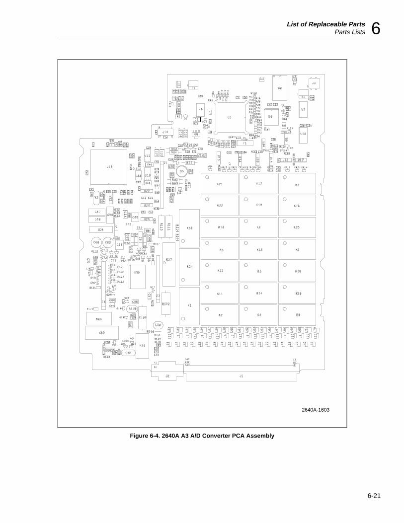
List of Replaceable PartsParts Lists 6
6-21
2640A-1603
Figure 6-4. 2640A A3 A/D Converter PCA Assembly
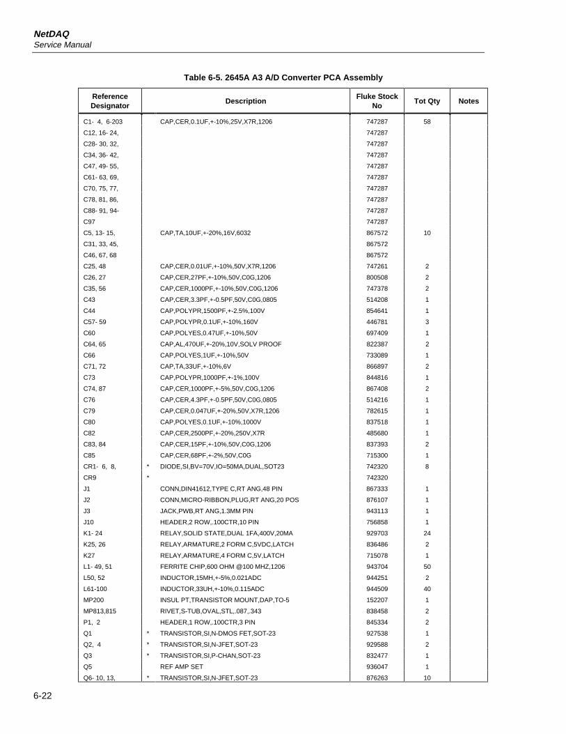
NetDAQService Manual
6-22
Table 6-5. 2645A A3 A/D Converter PCA Assembly
ReferenceDesignator
DescriptionFluke Stock
NoTot Qty Notes
C1- 4, 6-203 CAP,CER,0.1UF,+-10%,25V,X7R,1206 747287 58
C12, 16- 24, 747287
C28- 30, 32, 747287
C34, 36- 42, 747287
C47, 49- 55, 747287
C61- 63, 69, 747287
C70, 75, 77, 747287
C78, 81, 86, 747287
C88- 91, 94- 747287
C97 747287
C5, 13- 15, CAP,TA,10UF,+-20%,16V,6032 867572 10
C31, 33, 45, 867572
C46, 67, 68 867572
C25, 48 CAP,CER,0.01UF,+-10%,50V,X7R,1206 747261 2
C26, 27 CAP,CER,27PF,+-10%,50V,C0G,1206 800508 2
C35, 56 CAP,CER,1000PF,+-10%,50V,C0G,1206 747378 2
C43 CAP,CER,3.3PF,+-0.5PF,50V,C0G,0805 514208 1
C44 CAP,POLYPR,1500PF,+-2.5%,100V 854641 1
C57- 59 CAP,POLYPR,0.1UF,+-10%,160V 446781 3
C60 CAP,POLYES,0.47UF,+-10%,50V 697409 1
C64, 65 CAP,AL,470UF,+-20%,10V,SOLV PROOF 822387 2
C66 CAP,POLYES,1UF,+-10%,50V 733089 1
C71, 72 CAP,TA,33UF,+-10%,6V 866897 2
C73 CAP,POLYPR,1000PF,+-1%,100V 844816 1
C74, 87 CAP,CER,1000PF,+-5%,50V,C0G,1206 867408 2
C76 CAP,CER,4.3PF,+-0.5PF,50V,C0G,0805 514216 1
C79 CAP,CER,0.047UF,+-20%,50V,X7R,1206 782615 1
C80 CAP,POLYES,0.1UF,+-10%,1000V 837518 1
C82 CAP,CER,2500PF,+-20%,250V,X7R 485680 1
C83, 84 CAP,CER,15PF,+-10%,50V,C0G,1206 837393 2
C85 CAP,CER,68PF,+-2%,50V,C0G 715300 1
CR1- 6, 8, * DIODE,SI,BV=70V,IO=50MA,DUAL,SOT23 742320 8
CR9 * 742320
J1 CONN,DIN41612,TYPE C,RT ANG,48 PIN 867333 1
J2 CONN,MICRO-RIBBON,PLUG,RT ANG,20 POS 876107 1
J3 JACK,PWB,RT ANG,1.3MM PIN 943113 1
J10 HEADER,2 ROW,.100CTR,10 PIN 756858 1
K1- 24 RELAY,SOLID STATE,DUAL 1FA,400V,20MA 929703 24
K25, 26 RELAY,ARMATURE,2 FORM C,5VDC,LATCH 836486 2
K27 RELAY,ARMATURE,4 FORM C,5V,LATCH 715078 1
L1- 49, 51 FERRITE CHIP,600 OHM @100 MHZ,1206 943704 50
L50, 52 INDUCTOR,15MH,+-5%,0.021ADC 944251 2
L61-100 INDUCTOR,33UH,+-10%,0.115ADC 944509 40
MP200 INSUL PT,TRANSISTOR MOUNT,DAP,TO-5 152207 1
MP813,815 RIVET,S-TUB,OVAL,STL,.087,.343 838458 2
P1, 2 HEADER,1 ROW,.100CTR,3 PIN 845334 2
Q1 * TRANSISTOR,SI,N-DMOS FET,SOT-23 927538 1
Q2, 4 * TRANSISTOR,SI,N-JFET,SOT-23 929588 2
Q3 * TRANSISTOR,SI,P-CHAN,SOT-23 832477 1
Q5 REF AMP SET 936047 1
Q6- 10, 13, * TRANSISTOR,SI,N-JFET,SOT-23 876263 10
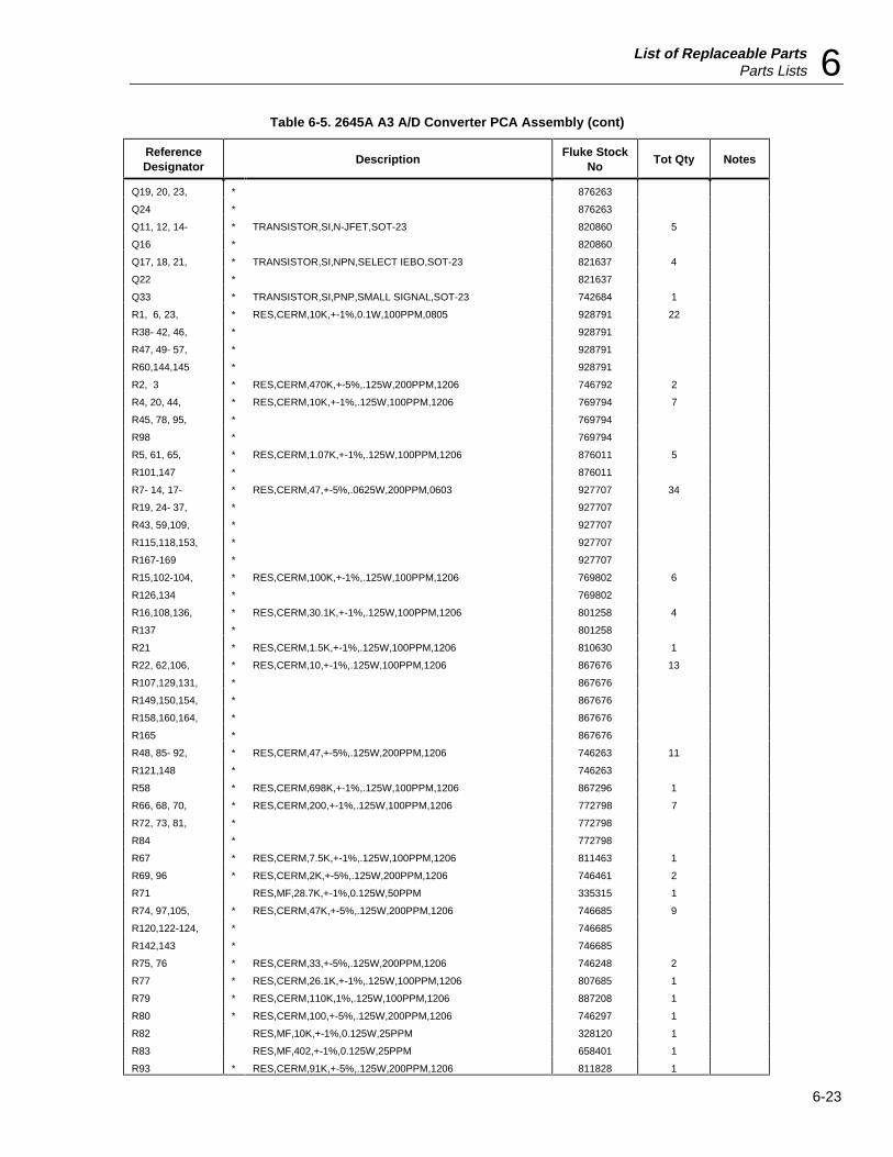
List of Replaceable PartsParts Lists 6
6-23
Table 6-5. 2645A A3 A/D Converter PCA Assembly (cont)
ReferenceDesignator
DescriptionFluke Stock
NoTot Qty Notes
Q19, 20, 23, * 876263
Q24 * 876263
Q11, 12, 14- * TRANSISTOR,SI,N-JFET,SOT-23 820860 5
Q16 * 820860
Q17, 18, 21, * TRANSISTOR,SI,NPN,SELECT IEBO,SOT-23 821637 4
Q22 * 821637
Q33 * TRANSISTOR,SI,PNP,SMALL SIGNAL,SOT-23 742684 1
R1, 6, 23, * RES,CERM,10K,+-1%,0.1W,100PPM,0805 928791 22
R38- 42, 46, * 928791
R47, 49- 57, * 928791
R60,144,145 * 928791
R2, 3 * RES,CERM,470K,+-5%,.125W,200PPM,1206 746792 2
R4, 20, 44, * RES,CERM,10K,+-1%,.125W,100PPM,1206 769794 7
R45, 78, 95, * 769794
R98 * 769794
R5, 61, 65, * RES,CERM,1.07K,+-1%,.125W,100PPM,1206 876011 5
R101,147 * 876011
R7- 14, 17- * RES,CERM,47,+-5%,.0625W,200PPM,0603 927707 34
R19, 24- 37, * 927707
R43, 59,109, * 927707
R115,118,153, * 927707
R167-169 * 927707
R15,102-104, * RES,CERM,100K,+-1%,.125W,100PPM,1206 769802 6
R126,134 * 769802
R16,108,136, * RES,CERM,30.1K,+-1%,.125W,100PPM,1206 801258 4
R137 * 801258
R21 * RES,CERM,1.5K,+-1%,.125W,100PPM,1206 810630 1
R22, 62,106, * RES,CERM,10,+-1%,.125W,100PPM,1206 867676 13
R107,129,131, * 867676
R149,150,154, * 867676
R158,160,164, * 867676
R165 * 867676
R48, 85- 92, * RES,CERM,47,+-5%,.125W,200PPM,1206 746263 11
R121,148 * 746263
R58 * RES,CERM,698K,+-1%,.125W,100PPM,1206 867296 1
R66, 68, 70, * RES,CERM,200,+-1%,.125W,100PPM,1206 772798 7
R72, 73, 81, * 772798
R84 * 772798
R67 * RES,CERM,7.5K,+-1%,.125W,100PPM,1206 811463 1
R69, 96 * RES,CERM,2K,+-5%,.125W,200PPM,1206 746461 2
R71 RES,MF,28.7K,+-1%,0.125W,50PPM 335315 1
R74, 97,105, * RES,CERM,47K,+-5%,.125W,200PPM,1206 746685 9
R120,122-124, * 746685
R142,143 * 746685
R75, 76 * RES,CERM,33,+-5%,.125W,200PPM,1206 746248 2
R77 * RES,CERM,26.1K,+-1%,.125W,100PPM,1206 807685 1
R79 * RES,CERM,110K,1%,.125W,100PPM,1206 887208 1
R80 * RES,CERM,100,+-5%,.125W,200PPM,1206 746297 1
R82 RES,MF,10K,+-1%,0.125W,25PPM 328120 1
R83 RES,MF,402,+-1%,0.125W,25PPM 658401 1
R93 * RES,CERM,91K,+-5%,.125W,200PPM,1206 811828 1
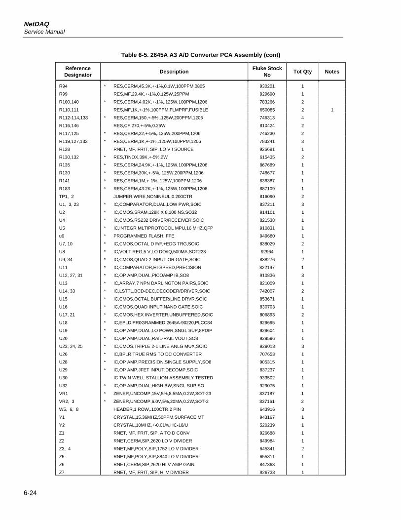
NetDAQService Manual
6-24
Table 6-5. 2645A A3 A/D Converter PCA Assembly (cont)
ReferenceDesignator
DescriptionFluke Stock
NoTot Qty Notes
R94 * RES,CERM,45.3K,+-1%,0.1W,100PPM,0805 930201 1
R99 RES,MF,29.4K,+-1%,0.125W,25PPM 929690 1
R100,140 * RES,CERM,4.02K,+-1%,.125W,100PPM,1206 783266 2
R110,111 RES,MF,1K,+-1%,100PPM,FLMPRF,FUSIBLE 650085 2 1
R112-114,138 * RES,CERM,150,+-5%,.125W,200PPM,1206 746313 4
R116,146 RES,CF,270,+-5%,0.25W 810424 2
R117,125 * RES,CERM,22,+-5%,.125W,200PPM,1206 746230 2
R119,127,133 * RES,CERM,1K,+-1%,.125W,100PPM,1206 783241 3
R128 RNET, MF, FRIT, SIP, LO V I SOURCE 926691 1
R130,132 * RES,TINOX,39K,+-5%,2W 615435 2
R135 * RES,CERM,24.9K,+-1%,.125W,100PPM,1206 867689 1
R139 * RES,CERM,39K,+-5%,.125W,200PPM,1206 746677 1
R141 * RES,CERM,1M,+-1%,.125W,100PPM,1206 836387 1
R183 * RES,CERM,43.2K,+-1%,.125W,100PPM,1206 887109 1
TP1, 2 JUMPER,WIRE,NONINSUL,0.200CTR 816090 2
U1, 3, 23 * IC,COMPARATOR,DUAL,LOW PWR,SOIC 837211 3
U2 * IC,CMOS,SRAM,128K X 8,100 NS,SO32 914101 1
U4 * IC,CMOS,RS232 DRIVER/RECEIVER,SOIC 821538 1
U5 * IC,INTEGR MLTIPROTOCOL MPU,16 MHZ,QFP 910831 1
u6 * PROGRAMMED FLASH, FFE 949680 1
U7, 10 * IC,CMOS,OCTAL D F/F,+EDG TRG,SOIC 838029 2
U8 * IC,VOLT REG,5 V,LO DO/IQ,500MA,SOT223 92964 1
U9, 34 * IC,CMOS,QUAD 2 INPUT OR GATE,SOIC 838276 2
U11 * IC,COMPARATOR,HI-SPEED,PRECISION 822197 1
U12, 27, 31 * IC,OP AMP,DUAL,PICOAMP IB,SO8 910836 3
U13 * IC,ARRAY,7 NPN DARLINGTON PAIRS,SOIC 821009 1
U14, 33 * IC,LSTTL,BCD-DEC,DECODER/DRIVER,SOIC 742007 2
U15 * IC,CMOS,OCTAL BUFFER/LINE DRVR,SOIC 853671 1
U16 * IC,CMOS,QUAD INPUT NAND GATE,SOIC 830703 1
U17, 21 * IC,CMOS,HEX INVERTER,UNBUFFERED,SOIC 806893 2
U18 * IC,EPLD,PR0GRAMMED,2645A-90220,PLCC84 929695 1
U19 * IC,OP AMP,DUAL,LO POWR,SNGL SUP,8PDIP 929604 1
U20 * IC,OP AMP,DUAL,RAIL-RAIL VOUT,SO8 929596 1
U22, 24, 25 * IC,CMOS,TRIPLE 2-1 LINE ANLG MUX,SOIC 929013 3
U26 * IC,BPLR,TRUE RMS TO DC CONVERTER 707653 1
U28 * IC,OP AMP,PRECISION,SINGLE SUPPLY,SO8 905315 1
U29 * IC,OP AMP,JFET INPUT,DECOMP,SOIC 837237 1
U30 IC TWIN WELL STALLION ASSEMBLY TESTED 933502 1
U32 * IC,OP AMP,DUAL,HIGH BW,SNGL SUP,SO 929075 1
VR1 * ZENER,UNCOMP,15V,5%,8.5MA,0.2W,SOT-23 837187 1
VR2, 3 * ZENER,UNCOMP,6.0V,5%,20MA,0.2W,SOT-2 837161 2
W5, 6, 8 HEADER,1 ROW,.100CTR,2 PIN 643916 3
Y1 CRYSTAL,15.36MHZ,50PPM,SURFACE MT 943167 1
Y2 CRYSTAL,10MHZ,+-0.01%,HC-18/U 520239 1
Z1 RNET, MF, FRIT, SIP, A TO D CONV 926688 1
Z2 RNET,CERM,SIP,2620 LO V DIVIDER 849984 1
Z3, 4 RNET,MF,POLY,SIP,1752 LO V DIVIDER 645341 2
Z5 RNET,MF,POLY,SIP,8840 LO V DIVIDER 655811 1
Z6 RNET,CERM,SIP,2620 HI V AMP GAIN 847363 1
Z7 RNET, MF, FRIT, SIP, HI V DIVIDER 926733 1

List of Replaceable PartsParts Lists 6
6-25
Table 6-5. 2645A A3 A/D Converter PCA Assembly (cont)
ReferenceDesignator
DescriptionFluke Stock
NoTot Qty Notes
Z8 RNET,MF,POLY,SIP,2280 LO V DIVIDER 611186 1
1. FUSIBLE RESISTOR. USE EXACT REPLACEMENT ONLY.
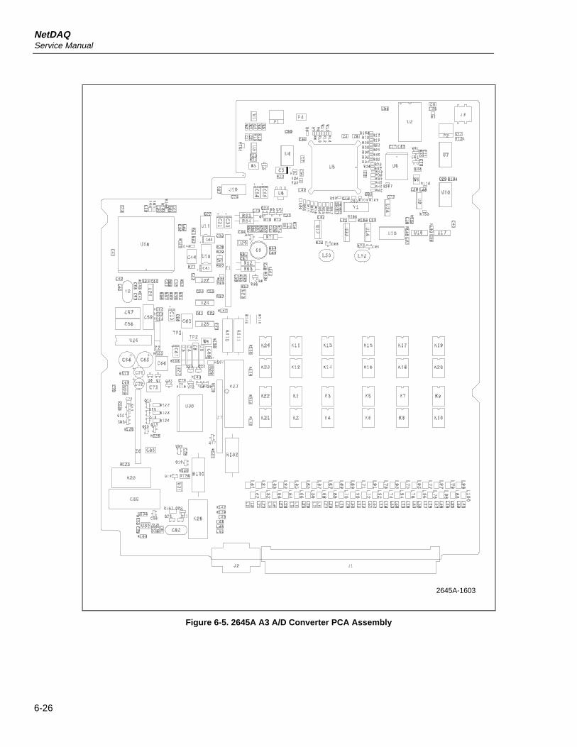
NetDAQService Manual
6-26
2645A-1603
Figure 6-5. 2645A A3 A/D Converter PCA Assembly
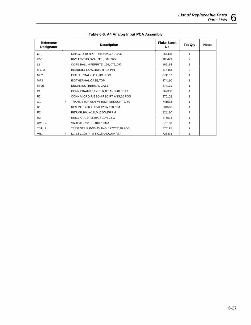
List of Replaceable PartsParts Lists 6
6-27
Table 6-6. A4 Analog Input PCA Assembly
ReferenceDesignator
DescriptionFluke Stock
NoTot Qty Notes
C1 CAP,CER,1000PF,+-5%,50V,C0G,1206 867408 1
H55 RIVET,S-TUB,OVAL,STL,.087,.375 106473 2
L1 CORE,BALUN,FERRITE,.136,.079,.093 106184 1
M1, 2 HEADER,1 ROW,.156CTR,15 PIN 414458 2
MP2 ISOTHERMAL CASE,BOTTOM 874107 1
MP3 ISOTHERMAL CASE,TOP 874110 1
MP25 DECAL,ISOTHERMAL CASE 874131 1
P1 CONN,DIN41612,TYPE R,RT ANG,48 SCKT 867338 1
P2 CONN,MICRO-RIBBON,REC,RT ANG,20 POS 876102 1
Q1 * TRANSISTOR,SI,NPN,TEMP SENSOR TO-92 741538 1
R1 RES,MF,5.49K,+-1%,0.125W,100PPM 334565 1
R2 RES,MF,10K,+-1%,0.125W,25PPM 328120 1
R3 RES,VAR,CERM,50K,+-10%,0.5W 876573 1
RV1- 4 VARISTOR,910,+-10%,1.0MA 876193 4
TB1, 2 TERM STRIP,PWB,45 ANG,.197CTR,20 POS 875195 2
VR1 * IC, 2.5V,100 PPM T.C.,BANDGAP REF 723478 1
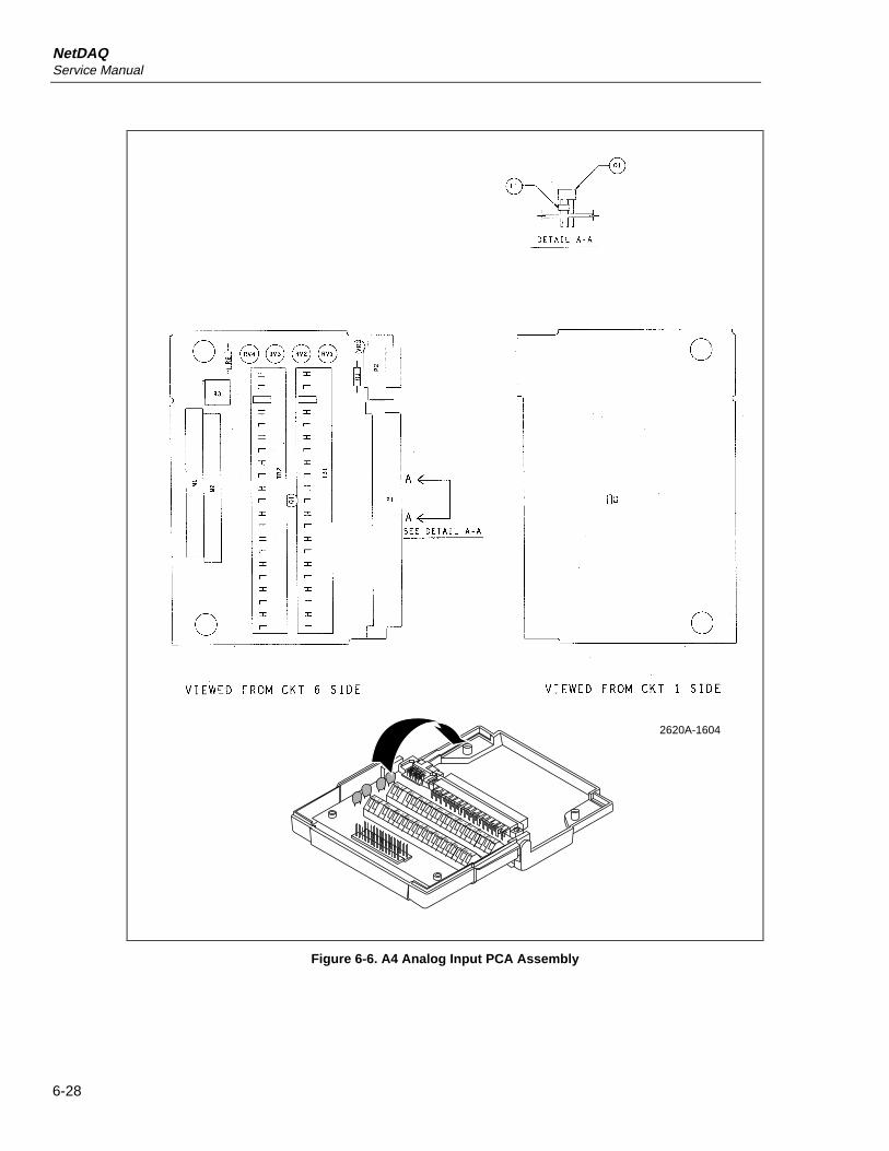
NetDAQService Manual
6-28
L
HL
H
HL
HL
HL
HL
HL
HL
HL
HL
L
HL
H
HL
HL
HL
HL
HL
HL
HL
HL
2620A-1604
Figure 6-6. A4 Analog Input PCA Assembly
7-1
Chapter 7Schematic Diagrams
Title Page
7-1. Introduction ............................................................................................ 7-37-2. A2 Display PCA Assembly.................................................................... 7-107-3. 2640A A3 A/D Converter PCA Assembly............................................. 7-127-4. 2645A A3 A/D Converter PCA Assembly............................................. 7-197-5. A4 Analog Input PCA Assembly ........................................................... 7-26

NetDAQService Manual
7-2
Schematic Diagrams 7
7-3
Figure 7-1. A1 Main PCA Assembly
REF DES
U36U2U22U23U14U15U29U20U30U34U35U10U32
U13U37U1
U16
U21U11U17, U27U33U31
DO_GND
8
GND
77 77771016161616316, 20, 29,30, 37, 56, 61, 65, 80,99, 120, 127,140, 143,144, 145, 146, 147,148, 149,150, 160994, 13, 23, 29, 34, 44, 57, 67, 84, 102,107, 116,126
13, 321, 12, 21
1416, 28, 53, 66, 77, 4
GND1
16, 17
IBIAS
1414
M9V
5, 6, 7, 8,9, 10, 11, 20, 21, 22,23, 24, 25
VBB
14
24
VCC
14
14
21, 19, 31, 32,52, 53, 62, 81, 116, 121
1616
2827, 41, 5579, 91, 3
VCC1
18, 28, 39,62, 83, 99,112, 131
VCC15
14
VCC20
32
VCC29
20
VCC30
32
VCC34
32
VCC35
32
VCC21
23
Reference Designations
Last Used
BTCCRDSJLPQRRTRVSTTPUVRWWPYZ
BT1C102CR22DS3J6L13P10Q10R148RT1RV2S1T4TP32U38VR3W5WP2Y2Z3
C66, 70, 72, 74, 85, 91, 94
J1
P4-9Q2-4
TP16-17, 19-29U26VR1-2
Not Used
NOTES: UNLESS OTHERWISE SPECIFIED
1. ALL CAPACITOR VALUES ARE IN MICROFARADS.2. ALL RESISTOR VALUES ARE IN OHMS.3. ALL RESISTORS ARE 1/8W, 5% UNLESS OTHERWISE NOTED.
2645A-1001(Sheet 1 of 7)
2645A-1601
2640A/2645AService Manual
7-4
R15
10
Q6MMBT3904
R4
10
HCU04
HCU04
D
HC74
CL
Q
Q
PR
TP30
CR6
MBR140
CR2
1N5397
CR5
MBR140
47C6
CR3
1N5397
.033C2
0.15 A
N
EG
L
J3
180PFC59
J2
P10
RT1
RXE135
1.0
C344.02KR46
11.0KR19
R20
59.0K
VCC
TP6
TP5
TP3
TP4
TP32
TP10
TP9
TP14
TP31
1N5235BVR3
47C5
U28LM358DT
MBRD360
CR1
R44
1.30K
TP7
U28LM358DT
12.4KR29
R48
10KC39
.047
10000
C7
220
C1
TP1
12.4KR30
WP1 WP2
12.4KR5
12.4KR6
220KR27
12.4KR31
A
TP2
GND VC
VIN VSW
FB
U9
LT1170
T1
MBRD360CR10
C102
.047MH2
MH1
4.02K
R12
4.02K
R131
1.21K
R11
R1321.21K
IN
ON
OUT
ADJ
GND
U25
LM2991T
R14
47K
ADJ
OUT
ON
IN
GND
U6
LM2941T
47
C26
1.30K
R10
4.02K
R9ADJ
OUT
ON
IN
GND
U24
LM2941T
R128
1.00K
R130
10
R13
1.00K
R129
4.02KR133
3.32K
1.0
C9
CR13MMBD7000
100R26
0.1C21
220C18
Q1MMBT3906
Q5MMBT3904
Q8SMD25N05
Q7SMD25N05
R38
0.02
47C30
47C31
2200C14
FLUKE45-6401T2
CR12
BAS16
D
HC74
CL
Q
Q
PR
R47
10K
1000PFC35
U18
LM79L05A
GND
OUTIN
HCU04HCU04HCU04HCU04
CR11
BAS16
R28
470
R34
470
R40
5.1K
MMBD7000CR9
CR8MMBD7000
LM317L
U19
IN OUT
ADJ
47KR22
2.2C17
1.0C32
VCC
470C13
470C12
CR7BAT54A
47C4
NOTE: U22 AND U23 ARE POWERED BYTHE OUTPUT OF U19.
SHEET 5
SHEET 7
UNUSED
INVERTER INGUARD SUPPLIES
5VAC
INVERTER OUTGUARD SUPPLIES
A/D
DIS
PLA
Y
5V SWITCHER
UNUSED
AUXILIARY 6V SUPPLY
TO REAR PANEL POWER SWITCH
INVERTER
RAW DC SUPPLY VPF
1%
1%
DCL
50V
1%
1%
U22
1
2
3
4
5
6
4
5
67
8
1
2
3
4
5
FIL1FIL2
50V
U23
1213
U23
1011
50V
1%
1%
U22
U23 U23 U23 U23
100V
100V
1/4W
50V
1%
35V10V
50V
VLOADVEE
VEE
50V1%1/4W
25V
1%
50V
35V
35V
100V
DCH
1/4W
SHLD
16V1% 1% VSS
1%
1%1%1%
VDD
RCOM
1%
1%
16V
1%
1%
VDDR
50V
50V
50V
7
8
45
10
69
1
4
6
23
7
1
8
1
2
3
4
5
6
7
8
10
11
12
8
9
10
11
12
13
1234568 9
24
79
1
2
3
12
3
4 5
12
3
4 5
12
3
4
5
12
3
4
8
2645A-1001(Sheet 2 of 7)
Figure 7-1. A1 Main PCA Assembly (cont)
Schematic Diagrams 7
7-5
C3
22PF
R2698K
C8
22PF
J2
47KR1
MC68302
U1
DTACKBCLR
BGBGACK
BRHALT
RESETAVEC/IOUT0
BERRIPL2/IRQ7IPL1/IRQ6IPL0/IRQ1
CLKO
EXTAL
XTAL
R/WAS
DS/LDSA0/UDS
IACK7/PB0IACK6/PB1IACK1/PB2
TIN1/PB3TOUT1/PB4
TIN2/PB5TOUT2/PB6
L1C
LK/R
CLK
1S
DS
1/L1
SY
0/T
CLK
1L1
TX
D/T
XD
1L1
RQ
/RTS
1/G
CID
CL
SP
TX
D/R
TS
3S
PC
LK/C
D3
BRG
1
BU
SW
DIS
CP
UF
RZ
PA
15/D
ON
EP
A14
/DA
CK
PA
13/D
RE
QP
A12
/BR
G3
PA
11/T
CLK
3P
A10
/RC
LK3
PA
9/T
XD
3P
A8
/RX
D3
PA
7/S
DS
2/B
RG
2P
A6
/CD
2P
A5
/RT
S2
PA
4/C
TS
2P
A3
/TC
LK
2P
A2/
RC
LK2
PA
1/T
XD
2P
A0
/RX
D2
L1R
XD
/RX
D1
L1G
R/C
TS1
L1SY1/CD1SPRXD/CTS3
D0D1D2D3D4D5D6D7D8D9D10D11D12D13D14D15
A23A22A21A20A19A18A17A16
A1
A2
A3
A4
A5
A6
A7
A8
A9
A10A11
A12
A13
A14
A15
PB
8P
B9
PB
10PB
11IA
C
FC
2FC
1F
C0
IOU
T2/
CS
0C
S1
CS
2C
S3
IOU
T1/R
MC
WD
OG
/PB
7
P10
VCC1
U13
D
U13
D
U13
MC145406DW
R
.1C40
.1C62
.1C64
VCC
.1C36
.1C41
R25
47K
VCC
R3
360
R8
470
R7
470
4.7
KR
7110
KR
7410
KR
75
VCC
10K
R79
10K
R81
4.7
KR
83
R21
270
47
R90
47
R93
47
R96
47
R66
47
R10
1
47
R10
2
47
R10
34
7R
104
47
R10
54
7R
106
TP13
TP15
TP8
TP12
J4
47
R10
84
7R
109
47
R110
R67 47R69 47R82 47R89 47R94 47R112 47R114 47
R116 47
R117 47R118 47R80 47R88 47R91 47R111 47R113 47R115 47
.1C24
0.01C27
0.01C37CR22
BAS16
360R16
U5
HCPL2601
U7
HCPL2601
R17 33
CD74AC04M
CD74AC32M
CD74AC32M
CD74AC32M
CD74AC32M
GAL16V8B-10LJ
CK/I0OE/I9
I8I7I6I5I4I3I2I1
F7F6F5F4F3F2F1F0
CD74AC04M
.1C16
.1C92
.1C93
U13
R
CD74AC04M
VCC
VCC
U13
D
CD74AC04M
CD74AC04M
CD74AC04M
10C101
W4
VCC
VCC1
U13
R
R43
10K
TP11
R125
0.02
R126
0.02
15.36 MHZY1
VCC
W1
W5
R13410K
R13510K
VCC L7
5UH
R143
47
R138 47R139 47
R140 47R141 47
R142
47
VCCL6
5UH
L8
5UHVCC
VCC1
47
R14
44
7R
145
R146 47R147 47R148 47
I/O AND MEMORY DECODER
RS
-23
2 I/F
DISPLAY
A/D
UNUSED
MICROPROCESSOR
W4 BOOT BAUD RATE
ON 38.4KOFF 19.2K
IN PRODUCTION ASSEMBLIES.NOTE: R125, W1, W4, W5 ARE NOT INSTALLED
SRAM DECODING
VCC15U15
25V
RAM*
RAM2*
RAM1*
A18*
20
18
1/4W
1/4WU14
3 4U15
1
23
U154
56
U14
1 2
UDS*
RESET
10
LDS*
1%
AS*
25V
U1
25V
U1
25V
U1
25V
U1
VCC29
U29
RESET*
B19.2K
87
9
SCLK
CINT*
DSCLKDCLK
DISRXDISTX
DRST*
HALT*
TOTINT*
PF
AIL
*B
19.2
K
VP
PE
NX
RD
YX
D/P
*X
INIT
*
DR
ST
*
DB
GR
XD
BG
TX
R/W*
RESET*
DS
CLK
DIS
TX
DTACK*
TXRX
DTR
DSR
CTSRTS
D<15..0>
RCOM 50V
VDDR
D<15..0>
50V
IGDS
IGDR
A<23..1>
10
32
654
87
91011121314
2019181716
15
R/W*LDS*
UDS*AS*I/O*ENET*
EIOW*RTC
EIOR*
PGA*WRU*RD1*
WRL*RD2*
U14
25V
U13
25V
25V
16VTANT
VEE
CONTROL
25V
U29
13 121415 1011 789 56 234 1
A<23..1>
RA
M*
EN
ET
*I/
O*
XT
INT
*K
INT
*E
INT
*D
ISR
XP
OR
*
FLS
H*
3
2
14121311105
9
876
109
1
11
5432
U14
5 6
U14
89
U14
1011
U14
1213
U15 89
10
U15 1112
13
1
23456789
11
1213141516171819
2
3
5
6
78
2
3
5
6
78
710
314
413
215
512
611
1235678910111214151617
1920212224252627
30313233353637384041424345464748
4950
51 52
53
54
55
56
58
59
60 61 63
64
65
66
68
69
70 71 72
73
74
76
77
78
79
80 81 82
85868788
909192939495969798
100
101
103104105106108109110111113114115
117
118
119
120
121
122
123
124
125
127
128
129
130
132
2645A-1001(Sheet 3 of 7)
Figure 7-1. A1 Main PCA Assembly (cont)
2640A/2645AService Manual
7-6
VCC
.1C75
.1C22
.1C63
.1C68
P2
R18
1.00K
UPD43256BGU-70L
OECSWE
A14A13A12A11A10A9A8A7A6A5A4A3A2A1A0
IO8IO7IO6IO5IO4IO3IO2IO1
R45
1.5K
R41
1.5K
R73
1.5K
R78
1.5K
R24
78.7
C33
.1
R42
39.2
R65
39.2
C69
.1
R85
39.2
R87
39.2
-9V
P1
R92
75
R100
75
R120
75
R32
75
C60
.1
R68
75
R76
75
R86
49.9
R95
49.9
12.4KR107 20.0 MHZ
Y2
22PFC89
22PFC38
1
.1C65
RDYPOLRDY
MODE0MODE1MODE2
AENALE
EOP
DREQDMACK
SMEMRD
INTSEL0INTSEL1
IRQA
IRQDIRQCIRQB
CHRESET
SD2SD1SD0
SD3
SD5SD4
SD6
SD10SD11SD12SD13SD14SD15
SB/SW
SA0SA1SA2SA3SBHE
ECS
SD9SD8SD7
IORIOW
MB86965APF
LEDC LEDL LEDT LEDR
TPIPTPIN
TPONBTPONA
TPOPBTPOPA
DON
BD7
DOPDOPDON
DIPDIN
CINCIP
RMTRSTCNTRL
BD8BD9
BD10BD11BD12BD13BD14BD15
BD6
BD1BD0
BD2BD3BD4BD5
BWEBCS0BCS1BOE
CLKOCLKIRBIAS
BA0
BA15
BA1BA2BA3BA4BA5BA6BA7BA8BA9
BA10BA11BA12BA13BA14
DS2
DS3
R121
470
R122
470
.01C61
1MR77
.001C23
R97
360 DS1
.1C25
4.7KR33
VCC
ENABLE
OUT+OUT+
OUT-OUT-
IN-IN-
IN+IN+
EPC1018HU38
1
VCC
10C99
10C98
10C100
VCC
1
HC125
L4
6T
RXI
TXO
CDS
RR-
RR+
HBE
CD-
CD+
RX-
RX+
TX+
TX-
U16NE83Q92A
-9V
T3
T3
PE-65728TT3
1:1
21:
T4PE-65746
RV2910V
R136
470
1000PFC10
L5
5UH
C28
.001
BAW56CR4
10KR137
VCC
/
/
/
ETHERNET INTERFACE
10BASE2
10BASE-T
25V
U16 U16
TPONA
U32
23456
10
171821
252834363839
424345464849
5455
57585960
6364
66676869707172737475767778798283
848586878889
909192
939495969798100101102103
104105106
107
108
112113114115117118119122
124125126
129
130131132133
134135136137
138
139
141142
151
152153
154155
156
157158159
1%
TPTD+
1%1/4W
1%1/4W
1%1/4W
1%1/4W
1%1/4W
1%1/4W
1%1/4W
25V 1%1/4W
TANT16V
CONTROL
A<23..1>
D<15..0>
D<15..0>
A<23..1>
CONTROL
1/4W1%
25V 1/4W1%
1/4W1%
1/4W1%25V
1%1/4W
TANT16V
1W 3KV
TPRD-
TPRD+
TPTD-
3KV
1600V
01
432
567
01234
65
U33
25V
U32
25V
U32
25V
U32
25V
U32
25V
8
121314
91011
321015
4
765
21
3
7
1%TANT16V
BD<7..0>
DOP
DON
DTACK*
EINT*
EIOR*EIOW*
TPIPTPONB
TPIN
DIPDIN
CINCIP
RESET
TPOPB
TPOPA
1
876
543
2
109
U2
1
23
12
910
1112
22
2324
1
2
3
4
12
13
14
15
18
19
26
28
U33
1
2
3456789
10
1112131516171819
20
21
22
23
2425
26
27
1
2 15
16
4
5 12
13
7
8 9
10
1
2
3
6
7
8 9
10
11
14
15
16
2640A-1001(Sheet 4 of 7)
Figure 7-1. A1 Main PCA Assembly (cont)
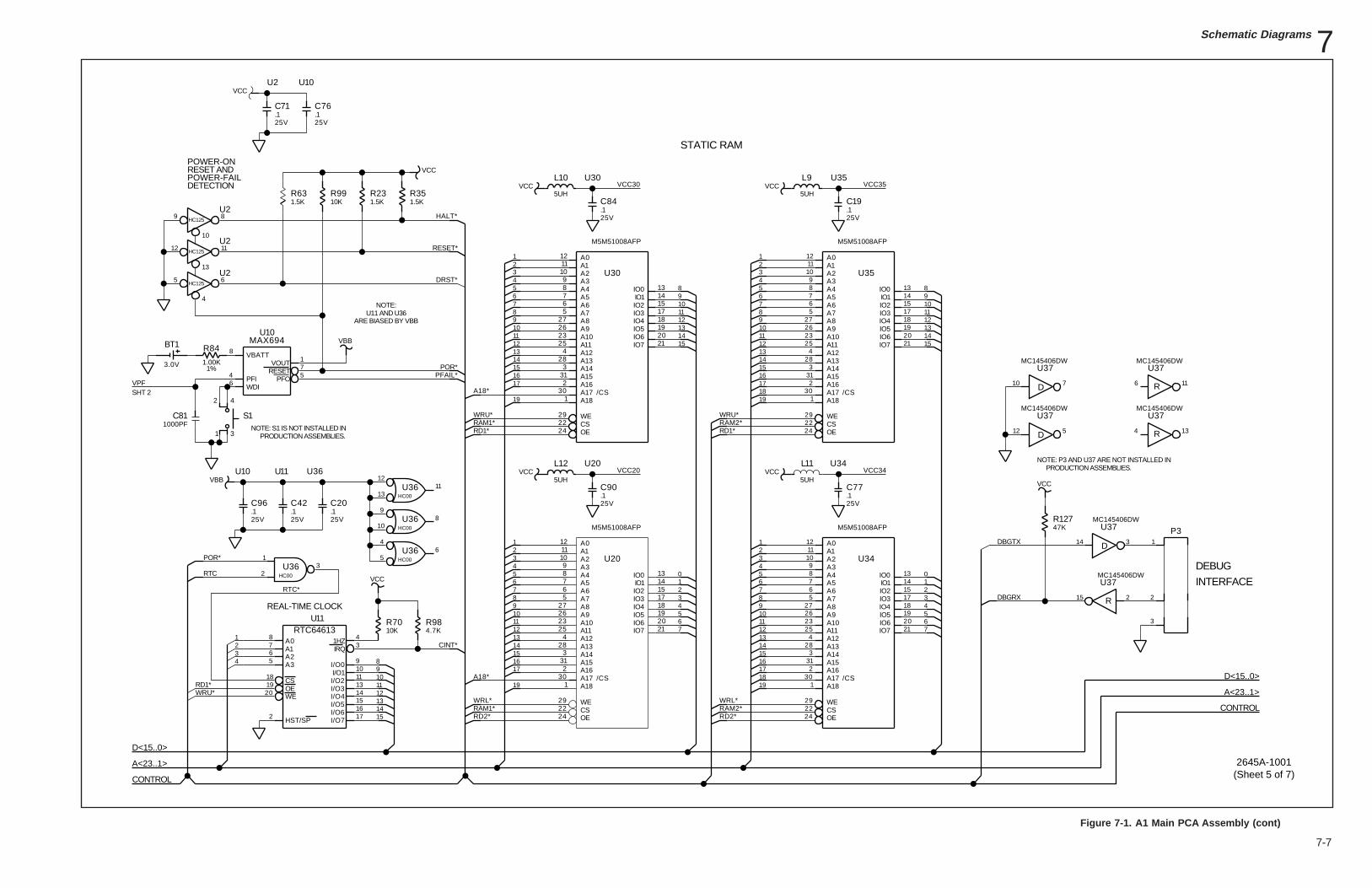
Schematic Diagrams 7
7-7
IO0IO1IO2IO3IO4IO5IO6IO7
A0A1A2A3A4A5A6A7A8A9A10A11A12A13A14A15A16
WECS
A18
OE
A17
U20
BT1
3.0VVBATT
PFIWDI
VOUTRESET
PFO
U10MAX694
HC125
HC125
HC00
10KR70
HC00
VCC
4.7KR98
HC00
HC00
.1C42
U11RTC64613
I/O7I/O6I/O5I/O4I/O3I/O2I/O1I/O0
WEOECS
IRQ1HZA0
A1A2A3
HST/SP
VCC
.1C71
.1C76
.1C84
.1C90
.1C96
VBB
.1C19
IO0IO1IO2IO3IO4IO5IO6IO7
A0A1A2A3A4A5A6A7A8A9A10A11A12A13A14A15A16
WECS
A18
OE
A17
U30
.1C20
10KR99
VCC
1.5KR23
1.5KR35
1000PFC81
VBBR84
1.00K
1.5KR63
HC125
.1C77
IO0IO1IO2IO3IO4IO5IO6IO7
A0A1A2A3A4A5A6A7A8A9A10A11A12A13A14A15A16
WECS
A18
OE
A17
U34
IO0IO1IO2IO3IO4IO5IO6IO7
A0A1A2A3A4A5A6A7A8A9A10A11A12A13A14A15A16
WECS
A18
OE
A17
U35
S1
U37MC145406DW
R
U37MC145406DW
R
U37MC145406DW
D
U37MC145406DW
D
U37MC145406DW
R
U37MC145406DW
D
P3
VCC
47KR127
VCCL11
5UH
L12
5UHVCC
VCCVCCL9
5UH
L10
5UH
STATIC RAM
INTERFACE
DEBUG
PRODUCTION ASSEMBLIES.NOTE: P3 AND U37 ARE NOT INSTALLED IN
REAL-TIME CLOCK
SHT 2
RESET ANDPOWER-ON
DETECTIONPOWER-FAIL
PRODUCTION ASSEMBLIES.NOTE: S1 IS NOT INSTALLED IN
/CS
/CS /CS
/CS
U11 AND U36ARE BIASED BY VBB
NOTE:
VCC35U35
25V
VCC34
25V
U34VCC20
25V
U20
VCC30U30
25V
RD2*RAM2*WRL*
1817
19
1615
1314
12
109
11
87654321
67
5432
01
RAM2*WRU*
RD1*
1819
1716
1415
131211
910
8
67
543
12
151413
10
12
9
11
8
RD1*RAM1*
A18*
WRU*
16
19
17
13
1514
1112
8910
67
3
54
12
1514
109
111213
8
RD2*
WRL*RAM1*
A18*17
19
1516
1312
14
109
11
87
456
23
1
65
7
4
0123
U36
25V
U11
25V25V
U10
POR*
RTC
25V
U2 U10
25V
4
23
1
1112131415
1098
RD1*
RTC*
POR*
CONTROL
CONTROL
PFAIL*VPF
1%
DBGRX
RESET*
HALT*
DRST*
WRU*
D<15..0>
CINT*
D<15..0>
A<23..1>
A<23..1>
DBGTX
M5M51008AFP
M5M51008AFP
M5M51008AFP
M5M51008AFP
1
2
3
U364
56
U36 1112
13
U36 89
10
U361
23
U21112
13
U289
10
U2
4
5 6
1
2
3
4
56789
101112
1314151718192021
22
23
24
25
2627
28
29
30
31
1
2
3
4
56789
101112
1314151718192021
22
23
24
25
2627
28
29
30
31
1
2
3
4
56789
101112
1314151718192021
22
23
24
25
2627
28
29
30
31
1
2
3
4
56789
101112
1314151718192021
22
23
24
25
2627
28
29
30
31
1
4 56
7
8
6 11
4 13
710
512
215
314
2
34
5678
910111314151617
181920
1
2
3
4
2645A-1001(Sheet 5 of 7)
Figure 7-1. A1 Main PCA Assembly (cont)
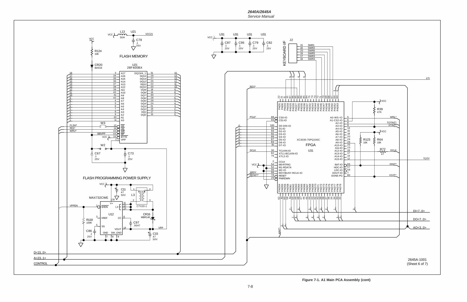
2640A/2645AService Manual
7-8
XC3030-70PQ100C
PWRDWNRESETRDY/BUSY-RCLK-IOM2-IOM1-RDATAM0-RTRIGCCLK
XTL2-IOXTL1-BCLKIN-IOTCLKIN-IO
D7-IOD6-IOD5-IOD4-IOD3-IOD2-IOD1-IOD0-DIN-IO
CS1-IOCS0-IO
DONE-PGDOUT-IO
LDC-IOHDC-IOINIT-IO
A15-IOA14-IOA13-IOA12-IOA11-IOA10-IOA9-IOA8-IOA7-IOA6-IOA5-IOA4-IOA3-IOA2-IO
A1-CS2-IOA0-WS-IO
PA
D5
3P
AD
52
PA
D5
0P
AD
49
PA
D4
8P
AD
47
PA
D4
6P
AD
45
PA
D4
4P
AD
43
PA
D4
2P
AD
37
PA
D3
6P
AD
35
PA
D31
PA
D2
7P
AD
26
PA
D2
5P
AD
16P
AD
15P
AD
6P
AD
5
PA
D7
9P
AD
78
PA
D7
7P
AD
76
PA
D7
5P
AD
74
PA
D7
3P
AD
72
PA
D71
PA
D7
0P
AD
69
PA
D6
8P
AD
67
PA
D6
6P
AD
65
PA
D6
4P
AD
63
PA
D6
2P
AD
61P
AD
58
PA
D5
6P
AD
55
PA
D5
4
J2
VCC
VCC
10KR123
47KR39
10KR64
R72
47
.1C78
.1C73
.1C67
VPP
CE
BYTE
WEOE
A0A1A2A3A4A5A6
A8A7
A9
A13A12A11A10
A14
A16A17
A15
DQ15/A_1
DQ0DQ1DQ2DQ3DQ4DQ5DQ6DQ7
DQ11
DQ9DQ8
DQ10
DQ12DQ13DQ14
RP
28F400BXU21
100KR119
.1C86
47C15
.0047C97
W2
MBR140CR16
LX
CC
VOUT
SW_GND
V+
SHDN
VREF
SS
GND
U12
MAX732CWE
VCC
47C11
L3
.1C79
.1C82
.1C87
.1C95
10KR124
BAS16CR20
VCC
VCC
VCC
VCC
L13
5UHVCC
W3
FPGA
KE
YB
OA
RD
I/F
FLASH PROGRAMMING POWER SUPPLY
FLASH MEMORY
FLSH*
CTX20-1
643
03
5
011 02
2343
55 4
6
7 6
7
2 1
76543210
1415
13
1112
10987
56
34
2
01
1718
1514
16
1312111098
67
54
21
3
RD1*
RD2*
A<23..1>
WRL*
AO<3..0>
KIN
T*
XRDYRESET*
SCLK
DO<7..0>
DI<7..0>
XINIT*
PGA*
TOTI*
SWR3SWR4
SWR1
SWR5SWR6SWR2
XTINT*
XTI
CONTROL
DCLK
XD/P*
TOTINT*
D<15..0>
50V
50V
25V
VPPEN
25V25V
BBVPPWRU*
VPP
U31
25V
U31
25V
U31
25V
U31
25V1516
18
1917
20
1
2 3
4
2
3
5
6
7 8 9
111213
14
16
1
3
456789
1011
1214
15
16
17
18
19
20
21
22
24
25
26
27
28
29
30
31
33
343536373839404142
4344
1
2
5689
1011
12
13
14
15
17
18
19
20
2122
23
24
2526
29
30
32
33
34
35
36
37
38
39
40
42
43
44
45
46
47
48
49
5051
5254
5657
58
59
606162
63
64
65
67
68
69
70
7172
73
74
75
76
78 80
81
82
83
84
85
86
87
88
89
90
92
93
94
95
96
97
98
99
100
25V
U21VCC21
U31
2645A-1001(Sheet 6 of 7)
Figure 7-1. A1 Main PCA Assembly (cont)
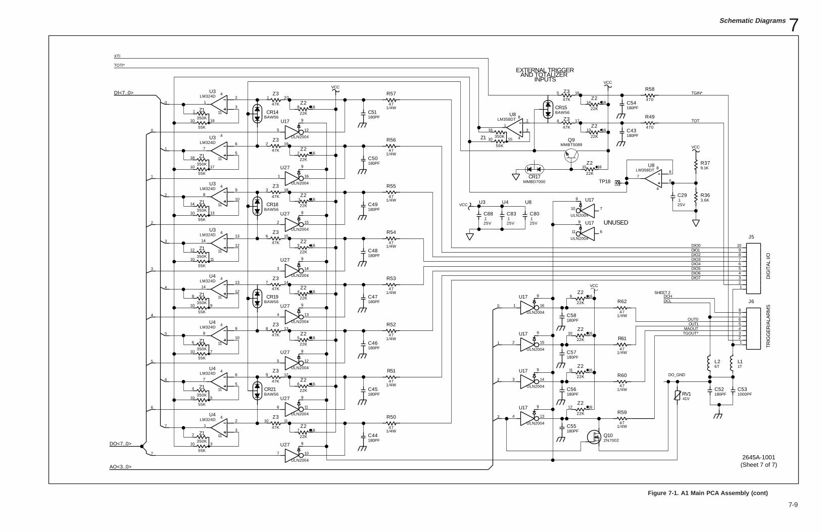
Schematic Diagrams 7
7-9
TP18
.1C80
.1C83
.1C88
180PFC55
180PFC56
180PFC57
180PFC58
180PFC52
1000PFC53
180PFC49
180PFC48
180PFC47
180PFC46
180PFC45
180PFC44
180PFC51
180PFC50
180PFC43
180PFC54
.1C29
VCC
VCC
VCCVCC
VCC
U3LM324D
U3LM324D
U3LM324D
U3LM324D
U4LM324D
U4LM324D
U4LM324D
U4LM324D
LM358DTU8
22K
Z2
22K
Z2
22K
Z2
22K
Z2
22K
Z2
22K
Z2
22K
Z2
22K
Z2
22K
Z2
22K
Z2
22K
Z2
22K
Z222K
Z2
22K
Z2
22K
Z2
RV141V
J6
J5
1TL1
6TL2
Z1
55K
350K
Z1
55K
350K
Z1
55K
350K
Z1
55K
350K
Z1
55K
350K
Z1
55K
350K
Z1
55K
350K
Z1
55K
350K
Z1
55K
350K
BAW56CR18
BAW56CR19
BAW56CR21
BAW56CR14 BAW56
CR15
Z3
47K
Z3
47K
Z3
47K
Z3
47K
Z3
47K
Z3
47K
Z3
47K
Z3
47K
Z3
47K
Z3
47K
MMBT5089Q9
CR17MMBD7000
R59
47
R60
47
R61
47
R62
47
R55
47
R54
47
R53
47
R52
47
R51
47
R50
47
R57
47
R56
47
R49
470
R58
470
9.1KR37
3.6KR36
ULN2004
U17
ULN2004
U17
ULN2004
U17
ULN2004
U17
ULN2004
U17
ULN2004
U17
ULN2004
U27
ULN2004
U27
ULN2004
U27
ULN2004
U27
ULN2004
U27
ULN2004
U27
ULN2004
U17
ULN2004
U27
LM358DTU8
Q102N7002
TR
IGG
ER
/ALA
RM
S
EXTERNAL TRIGGERAND TOTALIZER
DIG
ITA
L I/O
INPUTS
SHEET 2
UNUSED
TGIN*
1/4W
1/4W
1/4W
1/4W
1/4W
1/4W
1/4W
1/4W
1/4W
1/4W
1/4W
1/4W
7
6
5
4
3
7
6
5
4
2
1
0
3
2
1
0
3
2
1
0
AO<3..0>
OUT0OUT1
MAOUTTGOUT*
DO_GND
DO<7..0>
DI<7..0>
XTI
TOTI*
25V25V25V
25V
DCL
DIO0DIO1DIO2DIO3DIO4DIO5DIO6DIO7
DCH
TOT
U3 U4 U8
1
10
23456789
1
8
234567
12
3
4
11
4
5
67
11
4
89
1011
4
1112
1314
4
1112
1314
4
89
1011
4
5
67
11
12
3
4
11
4
5
67
8
12
3
4
8
12 16
11 16
10 16
9 16
7 16
6 16
5 16
4 16
3 16
1 16
2 16
8 1614 16
13 16
15 16
3 18
6 15
7 14
8 13
9 12
10 11
1 20
2 19
4 17
5 16
10 13
14
10 11
12
8
910
6
710
4
510
2
310
1
10 19
10 17
18
10 15
16
7
9
10
6
9
11
4
9
13
3
9
14
2
9
15
1
9
16
2
9
15
3
9
14
4
9
13
5
9
12
6
9
11
7
9
10
5
9
12
1
9
16
2645A-1001(Sheet 7 of 7)
Figure 7-1. A1 Main PCA Assembly (cont)
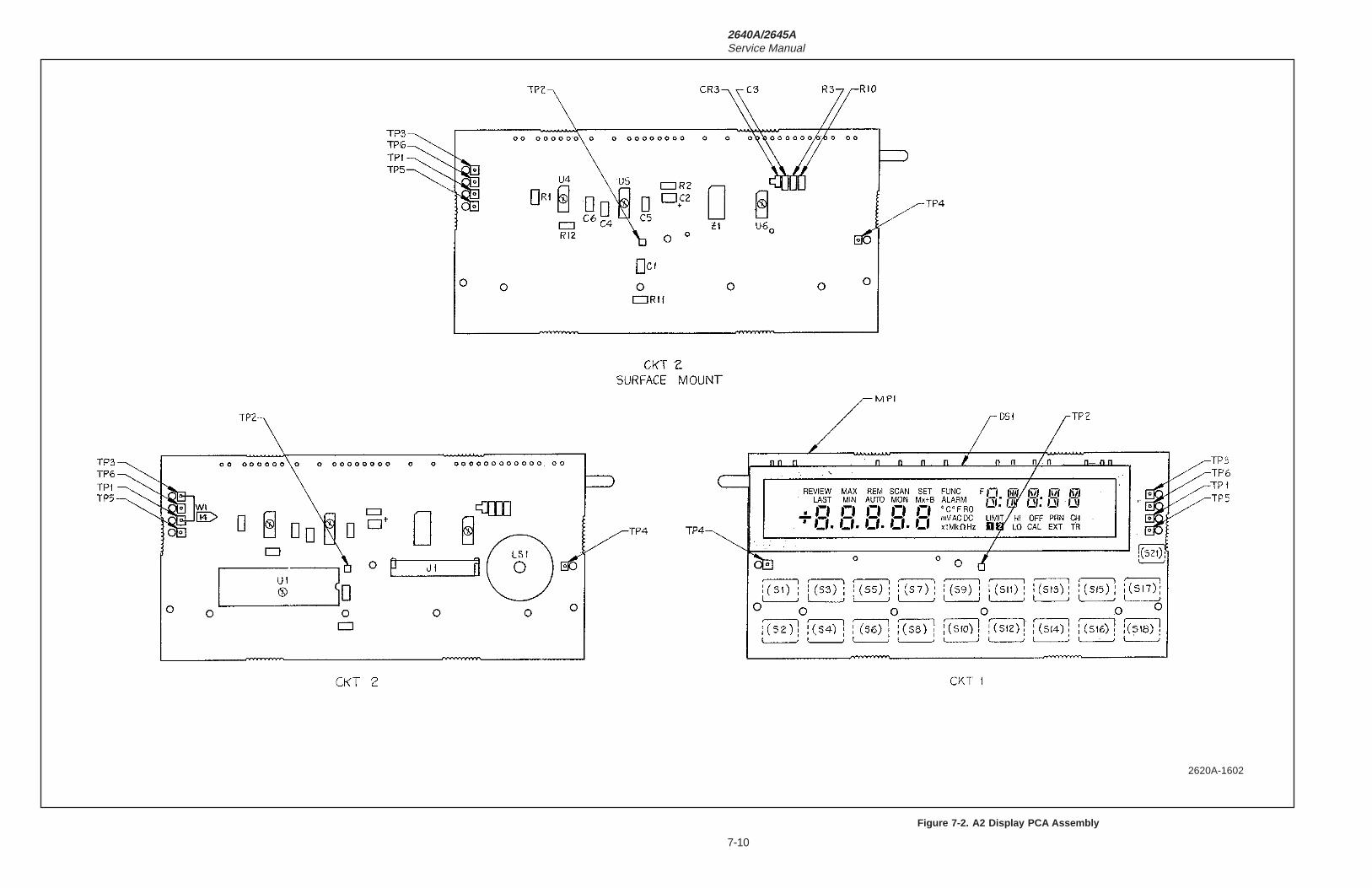
2640A/2645AService Manual
7-10
Figure 7-2. A2 Display PCA Assembly
2620A-1602
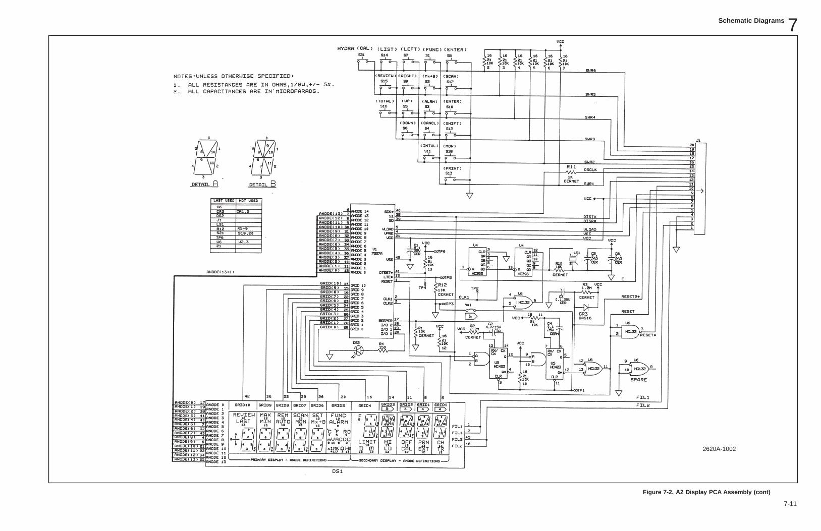
Schematic Diagrams 7
7-11
Figure 7-2. A2 Display PCA Assembly (cont)
2620A-1002
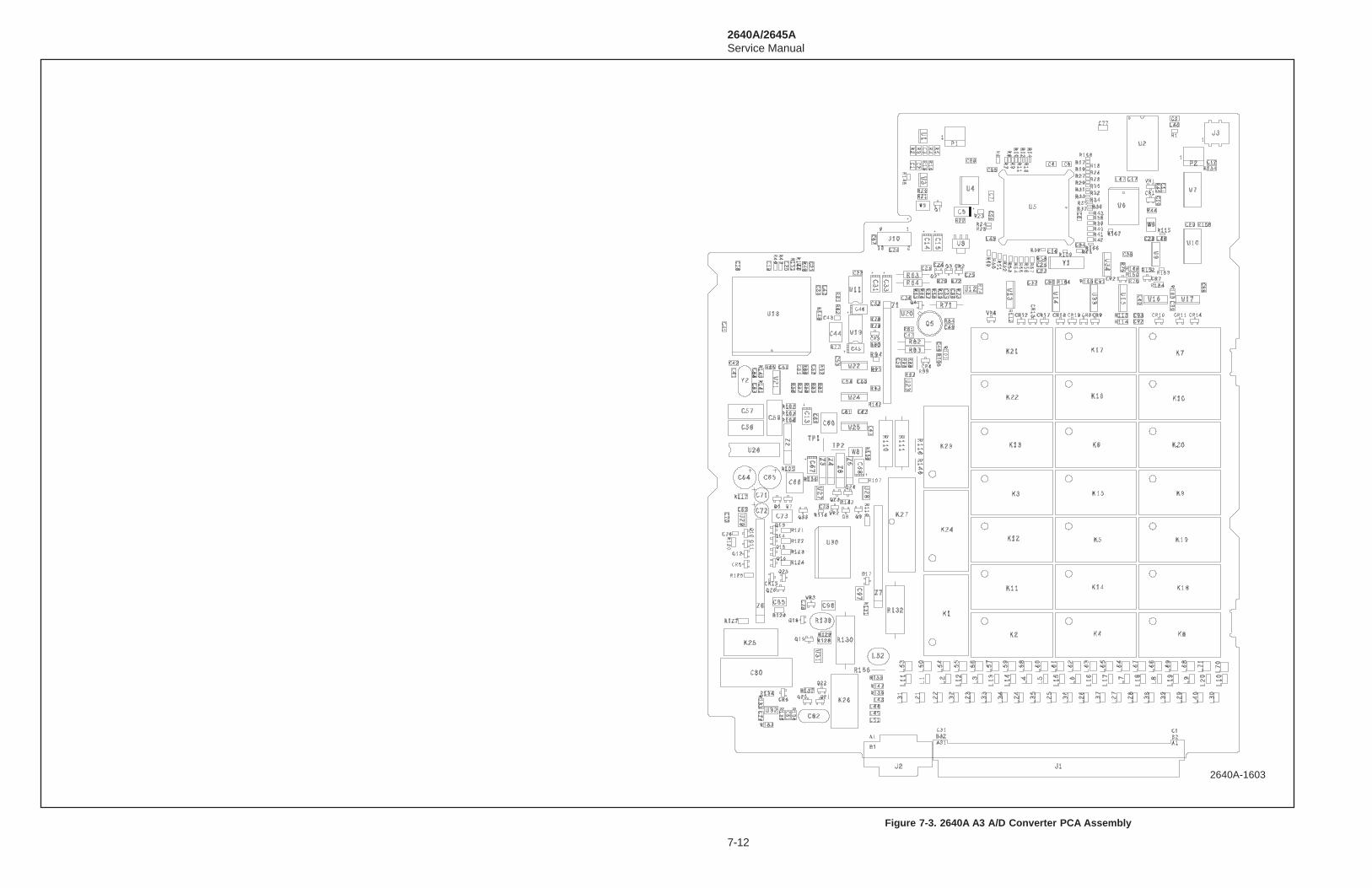
2640A/2645AService Manual
7-12 2640A-1603
Figure 7-3. 2640A A3 A/D Converter PCA Assembly
2640A-1603
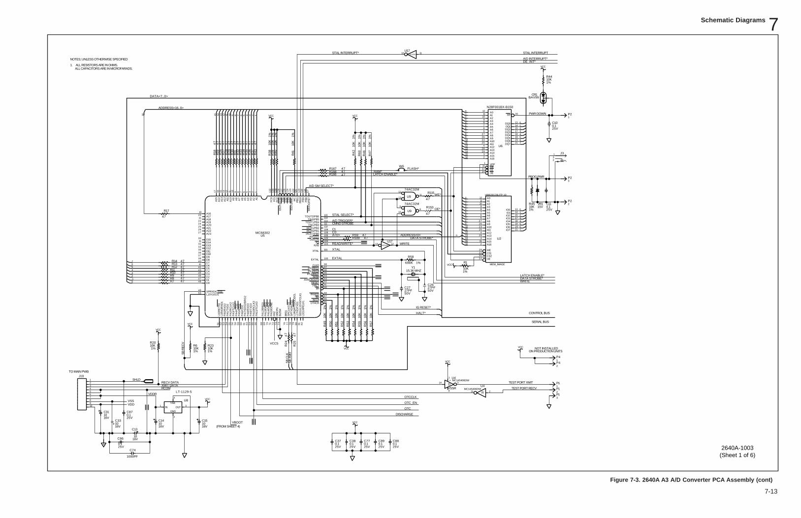
Schematic Diagrams 7
7-13
27PFC26
P1
10KR20
P1
P1
U9
74AC32M
U9
74AC32M
VCC
0.1C11
P2
0.1C10
10KR44
VCC
P2
HM628128LFP-10
MEM_IMAGE
OECS2CS1WE
A16A15A14A13A12A11A10A9A8A7A6A5A4A3A2A1A0
IO7IO6IO5IO4IO3IO2IO1IO0
J10
A
10C33
10C31
VR115V
VCC
47
R17
10C15
10C14
47R59
P2
BAV99CR1
47R747R847R947R1047R1147R1247R1347R14
47
R36
47
R34
47
R31
47
R37
47
R33
47
R30
47
R28
47
R27
47
R29
47
R43
47
R35
47
R32
47
R26
47
R19
HCU04
10
C13
10KR45
VCCR1
10K
10KR6
VCC
10K
R42
VCC
VCC
10K
R60
47
R24
47
R25
VCC
U4MC145406DW+
D
0.1C38
0.1C37
W6
10KR23
TAB
GND
OUTIN
U8
VCC
P4
P4
10K
R57
10K
R56
10K
R47
10K
R46 J3
0.1C87
0.1
C86
OE
WEVPP
CE
A16
A12A13A14A15
A11
A7A8A9A10
A2A3A4A5
A1A0
DQ0DQ1DQ2DQ3DQ4DQ5DQ6DQ7
A6
RP
N28F001BX-B150
U6
15.36 MHZY1
47
R153
47
R115
1000PF
C74
0.1C77
0.1C88
0.1C89
47R109
47R166
47R16747R168
47
R18
MC68302U5
DTACKBCLR
BGBGACK
BRHALT
RESETAVEC/IOUT0
BERRIPL2/IRQ7IPL1/IRQ6IPL0/IRQ1
CLKO
EXTAL
XTAL
R/WAS
DS/LDSA0/UDS
IACK7/PB0IACK6/PB1IACK1/PB2
TIN1/PB3TOUT1/PB4
TIN2/PB5TOUT2/PB6
L1C
LK/R
CLK
1S
DS
1/L1
SY
0/TC
LK1
L1TX
D/T
XD
1L1
RQ
/RTS
1/G
CID
CL
SP
TX
D/R
TS
3S
PC
LK/C
D3
BRG
1
BU
SW
DIS
CP
UFR
ZP
A15
/DO
NE
PA
14/D
AC
KP
A13
/DR
EQ
PA
12/B
RG
3
PA
11/T
CLK
3P
A10
/RC
LK3
PA
9/T
XD
3P
A8/
RX
D3
PA
7/S
DS
2/B
RG
2P
A6/
CD
2P
A5/
RT
S2
PA
4/C
TS
2P
A3/
TC
LK2
PA
2/R
CLK
2P
A1/
TX
D2
PA
0/R
XD
2L1
RX
D/R
XD
1L1
GR
/CTS
1
L1SY1/CD1SPRXD/CTS3
D0D1D2D3D4D5D6D7D8D9D10D11D12D13D14D15
A23A22A21A20A19A18A17A16
A1
A2
A3
A4
A5
A6
A7
A8
A9
A10A1
1A
12A
13A
14A
15
PB
8P
B9
PB
10PB
11IA
C
FC
2FC
1F
C0
IOU
T2/
CS
0C
S1C
S2
CS
3IO
UT1
/RM
C
WD
OG
/PB
7
U4MC145406DW
R
10K
R50
10K
R49
VCC
10K
R51
10K
R52
10K
R53
10K
R55
10K
R54
27PFC27
R58
698K
10K
R40
10K
R38
10K
R39
VCC
10K
R41
HCU04
1. ALL RESISTORS ARE IN OHMS. ALL CAPACITORS ARE IN MICROFARADS.
NOTES; UNLESS OTHERWISE SPECIFIED
NOT INSTALLEDON PRODUCTION UNITS
LT-1129-5
TO MAIN PWB
(FROM SHEET 4)
4
3
2
1
31
30
2928
2726
25
24
23
22
2120191817151413
1211
1098765
4
32
1
132
130
129
128
127
125
124
123
122
121
120
119
118
117
115114113111110109108106105104103
101
100
989796959493929190
88878685
82
8180
79
78
77
76
74
73
72
7170
69
68
66
65
64
63
6160
59
58
56
55
54
53
52
51
5049
48474645434241403837363533323130
2726252422212019
17 16 15 14 12 11 10 9 8 7 6 5 3 2 1
15 2
14
8
3
1
32
1
31
30
29
28
2726
25
24
23
22
2120191817151413
12111098765
4
3
213 12
1110
10
98
13
1211
2
1
3
1
2
3
1
2
10
12
43
5
76
98
1% 1% 1% 1% 1% 1% 1% 1% 1%
PROG PWR
RAM*
1%1%1%1%
LATCH ENABLE*
1%1%1%1%
CMND STROBEA/D TRIGGER*
READ/WRITE*
DATA STROBE*ADDRESS<0>A<0>
SB
XM
ITS
B C
LK
1%
SB
RE
CV
VBOOT
16V
VDDR
VSSVDD
VCC5
LATCH ENABLE*DATA STROBE*
50V
EXTAL
XTAL
50V
16V
25V
SHLD
25V25V
OTC
OTC_EN
OTCCLK
ADDRESS<16..0>
DATA<7..0>
PWR DOWN
25V
STAL SELECT*
A/D SM SELECT*
1%
FLASH*
16V
16V
TEST PORT RECV
1% 1%
A/D INTERRUPT*
STAL INTERRUPT* STAL INTERRUPT
DE_INT*
DISCHARGE
1% 25V
WRITE
RECV DATAXMIT DATARCOM
TEST PORT XMIT
C1C0
25V
HALT*
IG RESET*
CONTROL BUS
16V
25V 25V 25V
SERIAL BUS
0
21
43
67
5
01234567
10
U17
32
56
4
9
11
87
10
14
1615
1312
10
23
654
7
10
12
89
11
U2130141516
VSSR
1234567810 911121315 14
U17
16
765
234
10
WE*
OE*
WRITE
1%
1%
2640A-1003(Sheet 1 of 6)
Figure 7-3. 2640A A3 A/D Converter PCA Assembly (cont)
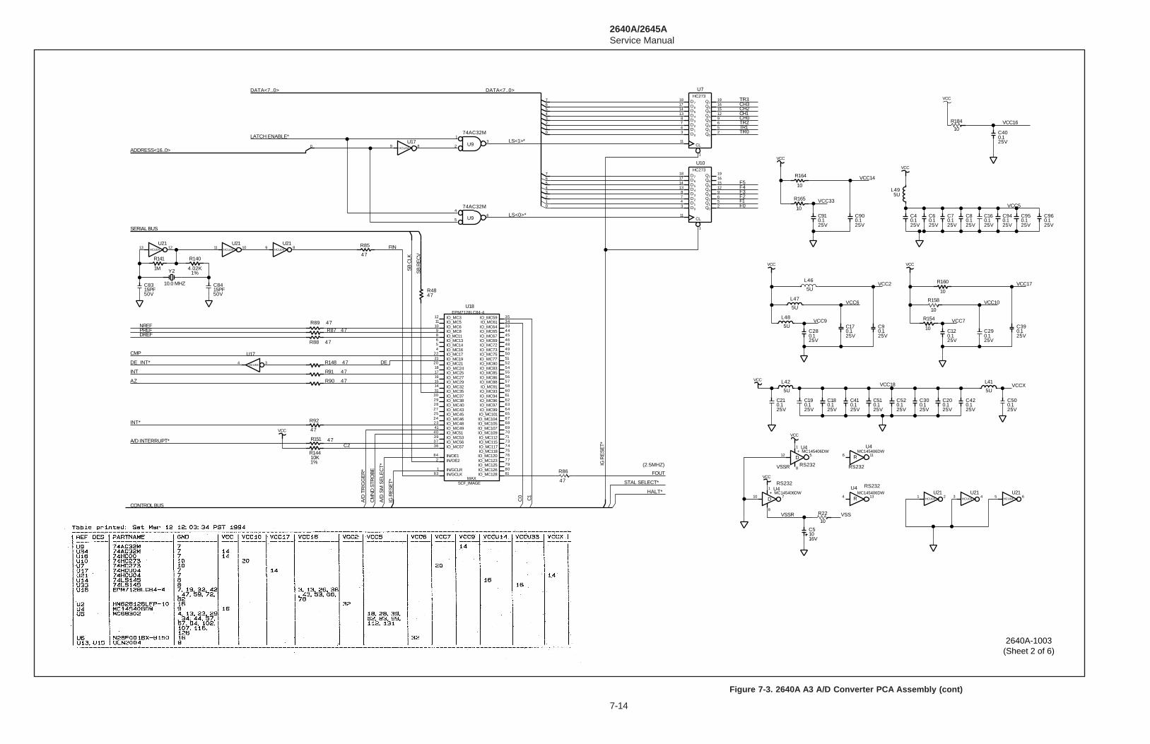
2640A/2645AService Manual
7-14
R22
10
10C5
0.1C42
0.1C20
0.1C30
0.1C6
0.1C18
0.1C41
0.1C51
0.1C52
HCU04
U9
74AC32M
0.1C50
0.1C28 0.1
C39
0.1C19
VCC
0.1C21
47
R86
47
R92
R4847
47
R85
47R91
47R90
47R88
47R87
47R89
HCU04HCU04
HCU04HCU04HCU04
HCU04
15PFC83
15PFC8410.0 MHZ
Y2
R140
4.02K
R141
1M
VCC
R14410K
VCC
U4MC145406DW
R
U4MC145406DW+
D
EPM7128LC84-4
MAXSCF_IMAGE
IN/GCLKIN/GCLR
IN/OE2IN/OE1
IO_MC57IO_MC56IO_MC53IO_MC51IO_MC49IO_MC48IO_MC46IO_MC45IO_MC43IO_MC40IO_MC38IO_MC37IO_MC35IO_MC32IO_MC29IO_MC27IO_MC25IO_MC24IO_MC21IO_MC19IO_MC17IO_MC16IO_MC14IO_MC13IO_MC11IO_MC8IO_MC6IO_MC5IO_MC3
IO_MC128IO_MC126IO_MC125IO_MC123IO_MC120IO_MC118IO_MC117IO_MC115IO_MC112IO_MC109IO_MC107IO_MC105IO_MC104IO_MC101IO_MC99IO_MC97IO_MC96IO_MC94IO_MC93IO_MC91IO_MC88IO_MC86IO_MC85IO_MC83IO_MC80IO_MC77IO_MC75IO_MC73IO_MC72IO_MC69IO_MC67IO_MC65IO_MC64IO_MC61IO_MC59
R148 47
R151 47
0.1C9
0.1C17
VCC
0.1C29
0.1C12
R154
10
VCC
R158
10
R160
10
VCC
0.1C16
0.1C7
0.1C4
0.1C8
VCC
0.1C90
0.1C91
R164
10
R165
10
L46
5U
L47
5U
L48
5U
L495U
L41
5U
L42
5U
0.1C94
HCU04
0.1C95
0.1C96
VCC
R184
10
0.1C40
HC273
CL
DDDDDDD
7
6
5
4
3
2
1
0
7
6
5
4
3
2
1
0
QQQQQQQQ
D
HC273
CL
DDDDDDD
7
6
5
4
3
2
1
0
7
6
5
4
3
2
1
0
QQQQQQQQ
D
U9
74AC32M
U4MC145406DW
R
VCC
U4MC145406DW+
D
(2.5MHZ)
IG R
ES
ET*
A/D
SM
SE
LEC
T*
CM
ND
STR
OB
E
A/D
TR
IGG
ER
*
C2
1% IG R
ES
ET*
RS232VSSR
VCC18
U10
U7
SB
RE
CV
SB
CLK
1%
U21
U17
U21 U21
0U17
RS232
RS232
23
01
65
7
4
12
0
3
67
45
U21 U21 U21
DE_INT*
TR3
CH0CH1CH2CH3
DATA<7..0>DATA<7..0>
TR1TR0
F5F4F3F2F1F0
TR2
LATCH ENABLE*LS<1>*
LS<0>*
50V 50V
ADDRESS<16..0>
SERIAL BUS
HALT*
STAL SELECT*
FIN
FOUT
NREFPREF
CMP
DREF
INT
AZ
INT*
CONTROL BUS
A/D INTERRUPT*
16V
VSSR VSS
25V25V25V25V25V25V25V25V25V25V
VCCX
25V25V25V
25V25V25V
VCC17
VCC10
VCC7
VCC2
VCC6
VCC9
25V25V25V
VCC14
VCC33
25V 25V 25V 25V 25V
VCC5
25V 25V
25V
VCC16
DE
C0 C1
RS232
4
56
1
23
1
11
18 191617
14 151213
8 967
4 523
1
11
18 191617
14 151213
8 967
4 523
89
891011
5 63 41 2
1213
34
U18
1
2
45689
101112
1415161718202122
2324252728293031
333435
3637394041
444546484950515254555657586061626364656768697071737475767779808183
84 6 11
1
5
8
12
4 13
1
7
8
10
2640A-1003(Sheet 2 of 6)
Figure 7-3. 2640A A3 A/D Converter PCA Assembly (cont)
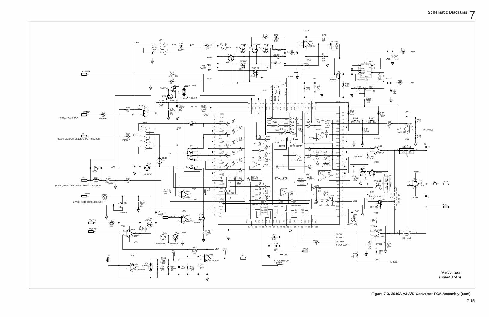
Schematic Diagrams 7
7-15
A
K27
2500PFC82
Q19
SB90041
R135
24.9K
A
100KR103
Q22
MPS6560
0.1C81
30.1KR136
.047C79
MPS6560
Q21
Q20SB90041
30.1KR137
R133
1.00K
100KR134
R102
100K
CR6BAV99
R129
10
R132
100K
A
MPS6560
Q17
A
R104
100K
R108
30.1K
A
R127
1.00K
0.1C59
18K
2K
54-4
118T
T
Z5
R1191.00K
A
33
C71
33
C72
470C65
470C64
1KR138
C732200PF
1.013K
Z6
12.25K
Z6
111.1KZ6
1.111M
Z6
47KR74
47KR97
47KR105
Q7
SB
9004
1
Q6
SB90041
A
U23
LM393DT
14K14K
54-4111TZ3
14K14K
54-4111TZ4
U29
LF357M
1K
Z7
10M
Z7
1M
100K
10K
1K
Z7
Z2
3.3K
AD706
U27
AD706
U31
AD706
U27
TP2
TP1
R125
22
A
R126
100K
A
A
R10710
R10610
47
R118
U26
AD637KD
DB
RMSOUTCHPSEL
OFFNUL
ACOMVIN
CAVDENIN
BUFIN BUFOUTVSP
VSM
LT1006
U28 W8
MC34072D
U32
MC34072D
U32
LM393DT
U23
U31
AD706
Q18
MPS6560
10C68
10
C67
2.776K
Z6
115.7
Z6
Q8
SB90041
Q23
SB90041
Z8
2.0K
14.0
K48
.336
K
R14347K
RELAY/STATUS PORT
RP1RP0
RP2RP3
RP5
RP7RP6
RP4
OSCILLATOR
G_AMP
FREQ_COMP
LO2
AGND
AG
ND
HGRD
HGRD
LGRD
LOV
LO1
IOUT
IG
S18
SGRD
IS
S46
NBIAS
HGRD
HGRD
AGND
BIAS
AGND
TCO
BIAS_AMP
AGND
BIAS
NBIAS
AC
FO
AC
FI
ACA-
HI
ACAO
ACA+
AGND
HGRD
HGRD
DCF2
HGRD
DCFO
DCFI
F_AMP
C-
HG
RD
C+
AC
R+
VD
D
VS
S
AC
R4
AC
R5
AC
R2
AC
R3
HRESET
FIN
BR+
DCA+
DCAO
DCA-
HGRD
BR-
BR1
BR2
BR3
BR4
LGRD
VDD
RESET
DGND
LGR
D
LO
G_AMP
LGRD
BR
S
SC
K
RC
V
SN
D
CS
*
SERIAL COMM
DG
ND
XO
UT
XIN
VS
S
RP
7
AC
R1
AC
R-
HG
RD
TR
HG
RD
HI2
HG
RD
HI1
VDD
V3S
V3
HGRD
SGRD
SGRD
V7
SGRD
V6S
V6
SGRD
V5S
V5
SGRD
V4S
V4
RP
6
RP
5
RP
4
RP
3
RP
2
RP1
RP
0
SGRD
V7S
LGRD
CTRI
DCLO
S1
S6
S11
S7
S2
S3
S8
S12
S13
S9
S4
S5
S10
S14
S15
S35
S24
S30
S23
S29
S22
S28
S21
S36
S37
S57B
S56B
S55B
S49
S48
S47
S45
S44
S62B
S39
S62A
S61A
S50
S43
S42S40
S41
S59B
S60BS60A
S59A
S58A
S19
DCHI
S31
S64
S20SOURCE1.2V, 3V
S27
S16
S17S65
S34
S26
S32
S33
S25
S54A
S57A
S56A S55A
S54B
S53
F_AMP
MRSTHRESET
RESET
189PFC1
VDD
SCKRCVBRS
HRESETCSSND
STALLION
S51
S52
S61B
S58B S63
S38
4.95K
Z2
R14510K
Q33
MMBT3906
R146
270
NB
C
SB90041
Q24
SB90041
Q9
R147
1.07K
A
R155
510
L52
15M
R18359.0K
A
A
R156
6.2K
180PFC98
CR15
MMBD7000
A
180PFC97
A
68PFC85
Q26
SB90041
Q25
SB90041
AA
C70
0.1
C69
0.1
0.1C78
0.1C58
VR36.0V
A
47
KR
121
47
KR
122
C76
4.3PF
R120
47K
R117
22
Q10
SSTH17
Q11
SSTH17
Q12
SSTH17
Q14
SSTH17Q15
SSTH17
SSTH17
Q16
47
KR
123
47
KR
124
Q13
SSTH17
VR2
6.0V
C75
0.1
A
A
A
A
BAV99CR5
A
3.45KR128
C80
0.1
1.0
C66
A
K25
R139
100K
R131
10
R130
100KK26
R111
1K0.1C57
R110
1K
VIATP5
TP6TP7 VIAVIA
54
-40
98
T
R
(FRDY)
(30VDC, 300VDC HI-SENSE, OHMS-HI-SOURCE)
(OHMS, .3VDC & 3VDC)
S
R
S
(30VDC, 300VDC-LO-SENSE, OHMS-LO-SOURCE)
(.3VDC, 3VDC, OHMS-LO-SENSE)
TP4VIA
R
S
10099989796959493929190898887868584838281
80
79
78
77
76
75
74
73
72
71
70
69
68
67
66
65
64
63
62
61
60
59
58
57
56
55
54
53
52
51
50 49 48 47 46 45 44 43 42 41 40 39 38 37 36 35 34 33 32 31
30
29
28
27
26
25
24
23
22
21
20
19
18
17
16
15
14
13
12
11
10
9
8
7
6
5
4
3
2
1
U30
3 21
4 3
87
97
32
1
74
75
76
1412
10
1311
9
8
64
7
53
8
64
1311
9
8
64
1311
9
8
4
3
21
8
76
5
4
8
7
6
5
4
3
2
1
8
4
3
21
8
76
5
4
7
6
4
3
2
87
65
4
3
21
11109
8
4
3
21
8
4
3
21
8
76
5
4
8
76
5
4
14
13
11
10
9
876543
1
3
2
1
3
2
1
3
2
1
4
3
2
1
2%50V
RGRD
1%
VCLAMP
VCLAMP
3W
1/4W
CH24CH24
1000V
CH24
VDD
1%
VDD
VSS
VDD
VSS
1%
OTC
VDD
1%
1%
VDD
VSS
1%
OTC_EN
OTCCLK
3W
LO
RJ SENSE
HI
FUSIBLE
VSS
VAC-
VDDB
AD HI
AD LO
RIVSSB
FUSIBLE
CH24
CH24
1%
1%
VAC-
VAC+
6V6V
25V
VAC+
ACR5
VAC- 25V
VDD
50V VAC-
VSS
1%
RI
VDD
VSS
1%
1%1%
160V
100V
+3.45V
STAL INTERRUPT
25V1%
HI SENSE
LO SENSE
250V
16V
VAC+
10V
10V
160V
160V
VDD
VDD
25V
SB RECV
STAL SELECT*
SB XMIT
SB CLK
DISCHARGE
1%
VDD
1%
25V
VSS
FOUT
VSS
VDDB
IG RESET*
1%
16V
VSSB
VDDVDD
VSS
50V
1%
LOW
VSSB
VDDB
1/4W
50V2%
50V2%
2640A-1003(Sheet 3 of 6)
Figure 7-3. 2640A A3 A/D Converter PCA Assembly (cont)
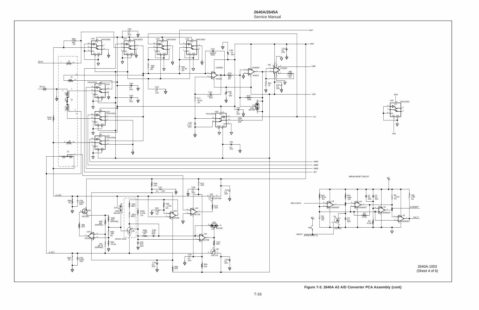
2640A/2645AService Manual
7-16
10KR4
0.1C3
30.1KR16
U3
LM393DT
100KR15
U3
LM393DT
R61
1.07K
U11
LT1016C
R2
470K
470KR3
0.1C2
U1
LM393DT
BAV99
CR2
BAV99CR3
U12
AD706
A
91K
R93
R8210K
AD822
AD822
Q4
SST109
A
CR4BAV99
A
R7128.7K
A
A
A0.1C22
0.1C32
0.1
C55
0.1
C54
A
R51.07K
VCC
14K 14K
Z1
44.97K
Z1
44
.97
K1
00
K6
.6K
Z1
89.97K
Z1
38.27K
Z1
74HC4053U24
VCC
GNDVEE
INH
R9929.4K
74HC4053U24VCC
GNDVEE
INH
74HC4053U24VCC
GNDVEE
INH
OP295
U20
OP295
U20
R9810K
R9510K
0.01C25
A
R211.5K0.1
C1
10C45
10C46
A
R9445.3K
A
74HC4053U22
VCC
GNDVEE
INH
A
A
0.1C23
0.1C24
R81200
R70200
R72200
R1011.07K
74HC4053U25
VCC
GNDVEE
INH
74HC4053U25
VCC
GNDVEE
INH
Q1
2N7002
VCC
W5
74HC4053U22VCC
GNDVEE
INH
74HC4053U22
VCC
GNDVEE
INH
74HC4053U25
VCC
GND VEE
INH
R83402
LM393DT
U1
A
A
0.1
C53
A
A
0.1
C63
0.1
C62
0.1
C61
R14247K
A
2640A-4501
Q5
R63SEL2
R64SEL1
R1004.02K
R68200
A
R692K
0.1C34
R84200
A
0.1
C49
U12
AD706
SST175
Q3
0.01C48
A
R67
7.5K
0.001C35
R651.07K
R66200
0.1
C47
A
A
A
Q2
SST109
0.1
C36
A
R73200
R962K
A
0.001C56
A
A
R80
100
0.47C60
A
R7726.1K
3.3PF
C43
R79
110KA
A
R6210
1500PF
C44
R78
10K A
A
(FROM SHEET 1)
BREAK-RESET CIRCUIT
LEADED
1%
LEADED
VDD
VSS
IG RESET*
HALT*
1%
25V
1%1%
VBOOT
RECV DATA
INT
PREF
NREF
DREF
AZ
50V
25V
25V25V
1%
1%1%
50V
1%
50V
AD LO
25V
25V
25V
1%
1%
16V50V
VSS
1%
CMP
VDD
INT*
16V100V
25V
1%
AD HI
+3.45V
25V
25V
50V
1%
25V 25V 1%
25V
25V
25V
-3.45V
50V
25PPM/C
50PPM/C
25PPM/C
1%
25V
1%
25V
34
56
7 8
9
16
6
7 8
11
12
1314
16
1
26
7 8
10
15
16
34
56
7 8
9
16
1
26
7 8
10
15
16
34
56
7 8
9
16
6
7 8
11
12
1314
16
1
26
7 8
10
15
16
6
78
11
12
1314
16
4
5
67
8
12
3
4
8
12
3
4
8
4
5
67
8
AC
CA
A
C
CA
A
C
CA
12
3
8 10
45
6
12
7 11
13
14
4
5
67
8
12
3
4
8
4
5
67
8
12
3
4
8
1
2
3
4
5
6
7
8
D
G
S
D
G
S
D
G
S
4
5
67
8
12
3
4
8
D
G
S
A
BC
E
2640A-1003(Sheet 4 of 6)
Figure 7-3. 2640A A3 A/D Converter PCA Assembly (cont)
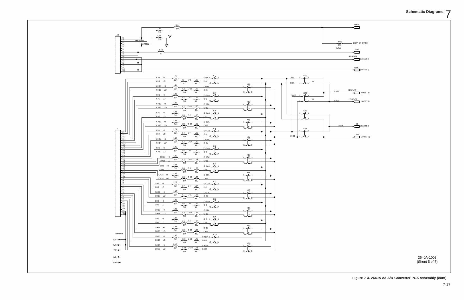
Schematic Diagrams 7
7-17
A
A
L19
5U
L9
5U
L18
5U
R116
270
L8
5U
J2
K10
K17
K18
K19
K20
K9
K8
K7
K2
K3
K4
K5
K6
K16
K15
K14
K13
K12
K11
K1
WP3
WP1
L50
33U
K22
K24
K23
K21
L43
5U
L44
5U
L45
5U
L51
5U
L71
33U
L70
33U
L69
33U
L68
33U
L67
33U
L66
33U
L65
33U
L64
33U
L63
33U
L62
33U
L61
33U
L60
33U
L59
33U
L58
33U
L57
33U
L56
33U
L55
33U
L54
33U
L53
33U
L40
5U
L29
5U
L39
5U
L30
5U
L24
5U
L25
5U
L26
5U
L34
5U
L35
5U
L36
5U
L27
5U
L37
5U
L38
5U
L28
5U
L31
5U
L32
5U
L33
5U
L21
5U
L22
5U
L23
5U
WP2
WP4
WP5
J1
L17
5U
L7
5U
L16
5U
L6
5U
L15
5U
L5
5U
L14
5U
L4
5U
L13
5U
L3
5U
L12
5U
L2
5U
L20
5U
L11
5U
L1
5U
L10
5U
(SHEET 3)
(SHEET 3)
(SHEET 3)
(SHEET 3)
(SHEET 3)
(SHEET 3)
(SHEET 3)
1/4W
LOW
CH20
CH10
CH19
CH9
CH18
CH8
CH17
CH7
CH16
CH6
CH15
CH5
CH14
CH4
CH13
CH3
CH12
CH2
CH11
CH22
CH22
CH21
CH21
RGRD
CH23
CH23
HI SENSE
LO SENSE
HI
LO
VDD
RJ RTRN
REF RTRN
RJ SENSE
SHLD
CH24
1U
1UCH1
CH11
CH2
CH1
CH12
CH3
CH13
CH4
CH14
CH5
CH15
CH6
CH16
CH7
CH17
CH8
CH18
CH9
CH19
CH10
CH20
CH1 HI CH1A
CH11A
CH2A
CH12A
CH3A
CH13A
CH4A
CH14A
CH5A
CH15A
CH6A
CH16A
CH7A
CH17A
CH8A
CH18A
CH9
CH19
CH10A
CH20A
B1
B2
B10
A1
A2
A3B3A4B4A5B5A6B6A7B7A8B8A9B9A10
B24
A3B2
A1B22
C1
B4A5
C3C5A7
C31
C7B6B8A9C11C9
A13C13B10
A11
B32
A15B16B14B12
C15
A17C19
B18
C17
B20
B30
C25A21A19C21
A25C23A23C29A29C27
B28
A27
A31
B26
5 6
3 4
5 6
3 4
5 6
3 4
5 6
3 4
5 6
3 4
5 6
3 4
5 6
3 4
5 6
3 4
5 6
3 4
5 6
3 4
5 6
3 4
5 6
3 4
5 6
3 4
5 6
3 4
5 6
3 4
5 6
3 4
5 6
3 4
5 6
3 4
5 6
3 4
5 6
3 4
5 6
3 4
5 6
3 4
5 6
3 4
5 6
3 4
CHASSIS
CH1 LO
CH11 HI
CH11 LO
CH2 HI
CH2 LO
CH12 HI
CH12 LO
CH3 HI
CH3 LO
CH13 HI
CH13 LO
CH4 HI
CH4 LO
CH14 HI
CH14 LO
CH5 HI
CH5 LO
CH15 HI
CH15 LO
CH6 HI
CH6 LO
CH16 HI
CH16 LO
CH7 HI
CH7 LO
CH17 HI
CH17 LO
CH8 HI
CH8 LO
CH18 HI
CH18 LO
CH9 HI
CH9 LO
CH19 HI
CH19 LO
CH10 HI
CH10 LO
CH20 HI
CH20 LO
2640A-1003(Sheet 5 of 6)
Figure 7-3. 2640A A3 A/D Converter PCA Assembly (cont)
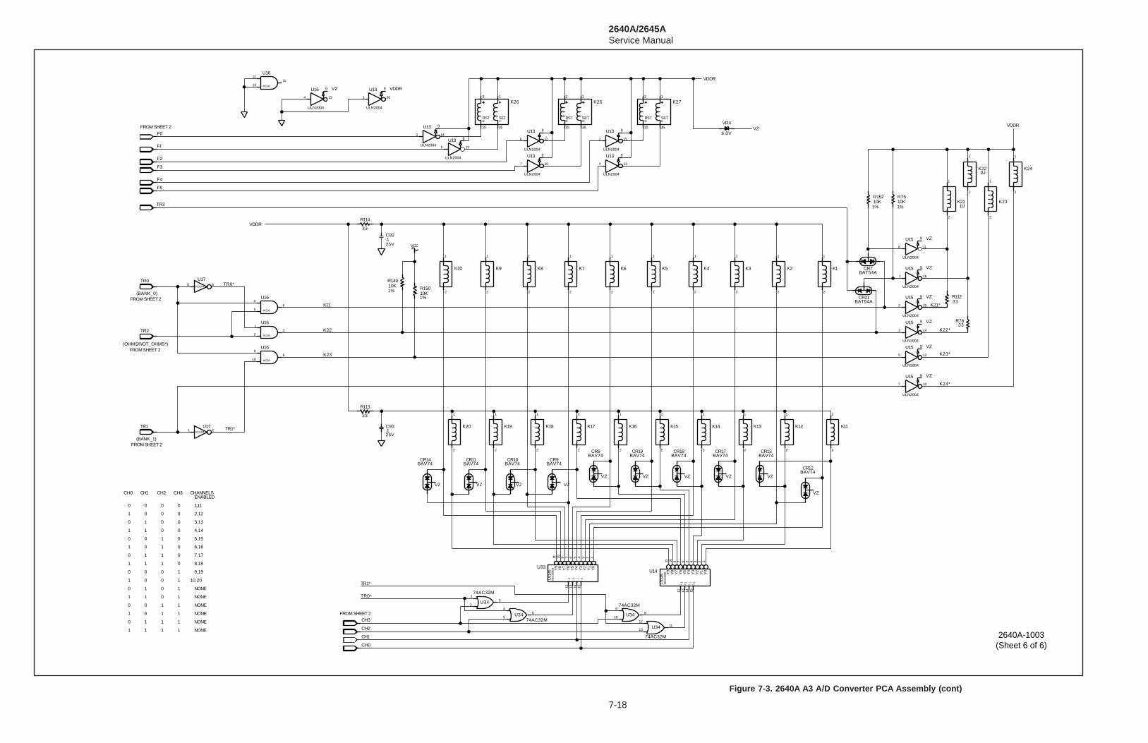
2640A/2645AService Manual
7-18
ULN2004
U15
HCU04
HC08
HC08
HC08
K1K2K3K4K5K6K7K8K9K10
K20 K11K12K13K14K15K16K17K18K19
CR14BAV74
CR8BAV74
CR9BAV74
CR10BAV74
CR11BAV74
VR4
6.0V
K21
K22
K23
K24
ULN2004
U15
ULN2004
U15
VCC
R14910K R150
10K
ULN2004
U15
ULN2004
U15
ULN2004
U15
ULN2004
U15
ULN2004
U13
I
Y Y Y Y Y Y Y Y013456789
LS14
5D
EC
OD
ER
3
2
YY
I I I2 1 0
CR12BAV74
CR13BAV74
CR17BAV74
CR18BAV74
CR19BAV74
BAT54ACR21
R15210K
R7510K
BAT54ACR7
R7633
R11233
U34
74AC32M
U3474AC32M
U34
74AC32M
U34
74AC32M
R113
33
R114
33
.1C92
.1C93
HC08
ULN2004
U13ULN2004
U13
K26
SETRST
I
Y Y Y Y Y Y Y Y013456789
LS14
5D
EC
OD
ER
3
2
YY
I I I2 1 0
ULN2004
U13
ULN2004
U13
ULN2004
U13
ULN2004
U13
K25
SETRST
K27
SETRST
HCU04
(BANK_1)
(BANK_0)
6,16
5,15
4,14
3,13
2,12
1,11
ENABLEDCHANNELS
0
0
0
0
0
0
CH3
1
1
0
0
0
CH1 CH2
0
0
1
1
0
0
0
1
0
1
0
1
0
CH0
0 7,17011
NONE
NONE
NONE
NONE
NONE
NONE
10,20
9,19
8,18
1
1
1
1
1
1
1
1
01 1
0 0
00
1 0
01
1
1
10
10
1
1
1
0
1
0
0
1
1
0
1
FROM SHEET 2
FROM SHEET 2
FROM SHEET 2
(OHMS/NOT_OHMS*)FROM SHEET 2
FROM SHEET 2
TR2
1%
1%
K24*
K23*
K22*
VDDR
1% 1%
VZ
K21*
VZ
VDDR
25V
VDDR
U17
U16
F0
F1
F2
F3
F4
F5
TR3
TR0
TR1*TR1
CH2
CH3
CH0
CH1
U14
U17
U16
U16
U16
VZ VZ VZ
VZ VDDR
VZ
VZ VZ VZ VZ VZ
VZ
VZ
VZ
VZ
VZ
VZ
K21
K22
K23
TR1*
TR0*
TR0*
25V
1U
1U
1
23
4
56 8
9
10
1112
13
4
56
89
10
1
23
1112
13
1 2
5 6
U33
123456791011
12 13 14 15
123456791011
12 13 14 15
1
2
1
2
1
2
1
2
1
2
1
2
1
2
1
2
1
2
1
2
1
2
1
2
1
2
1
2
1
2
1
2
1
2
1
2
1
2
1
2
1
2
1
2
1
2
1
2
12
15 16
12
15 16
12
15 16
6
9
11
4
9
13
2
9
15
5
9
12
7
9
10
3
9
14
1
9
16
1
9
16
5
9
12
3
9
14
7
9
10
6
9
11
4
9
13
2
9
15
2640A-1003(Sheet 6 of 6)
Figure 7-3. 2640A A3 A/D Converter PCA Assembly (cont)
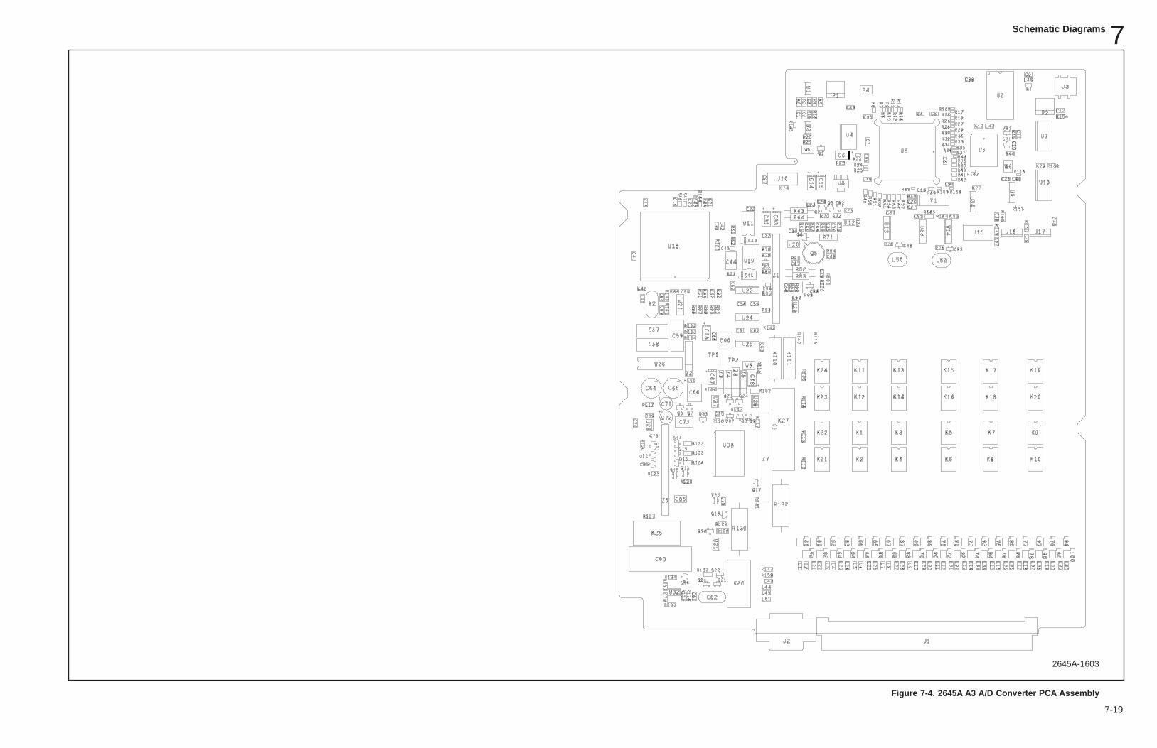
Schematic Diagrams 7
7-19
2645A-1603
Figure 7-4. 2645A A3 A/D Converter PCA Assembly
2645A-1603
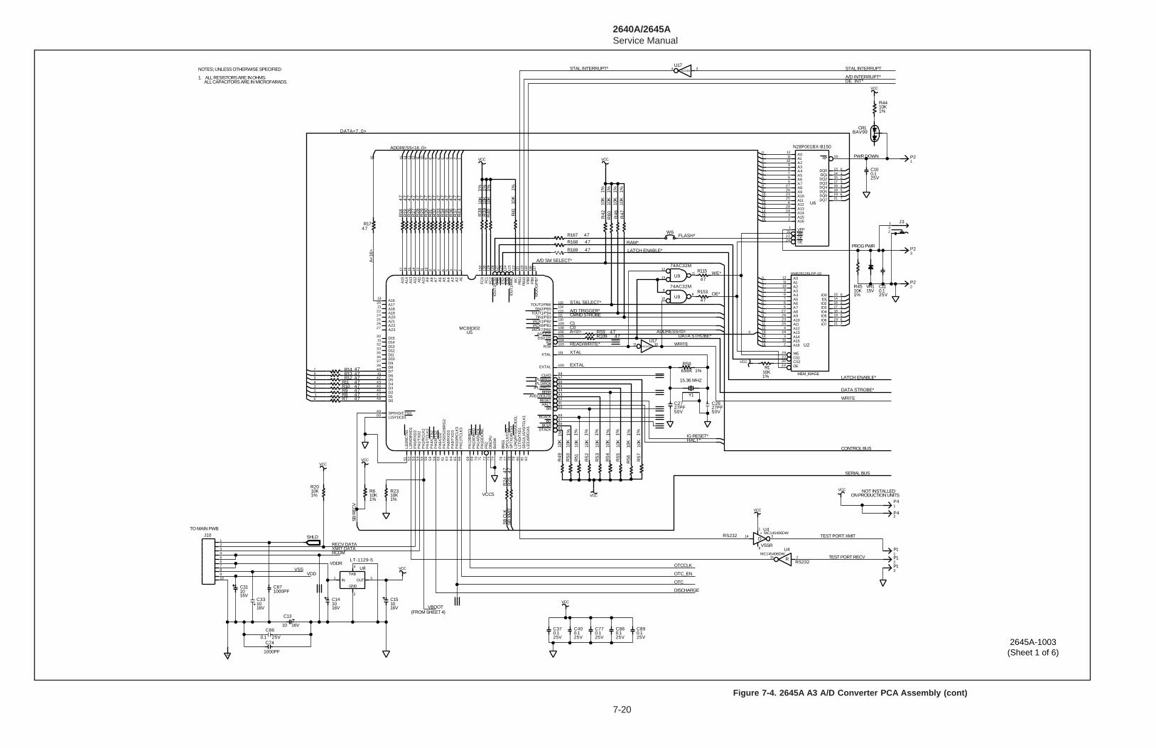
2640A/2645AService Manual
7-20
27PFC26
P1
10KR20
P1
P1
U9
74AC32M
U9
74AC32M
VCC
0.1C11
P2
0.1C10
10KR44
VCC
P2
HM628128LFP-10
MEM_IMAGE
OECS2CS1WE
A16A15A14A13A12A11A10A9A8A7A6A5A4A3A2A1A0
IO7IO6IO5IO4IO3IO2IO1IO0
J10
A
10C33
10C31
VR115V
VCC
47R17
10C15
10C14
47R59
P2
BAV99CR1
47R747R847R947R1047R1147R1247R1347R14
47
R36
47
R34
47
R31
47
R37
47
R33
47
R30
47
R28
47
R27
47
R29
47
R43
47
R35
47
R32
47
R26
47
R19
HCU04
10
C13
10KR45
VCC
R110K
10KR6
VCC
10K
R42
VCC
VCC
10K
R60
47
R24
47
R25
VCC
U4MC145406DW+
D
0.1C37
W6
10KR23
TAB
GND
OUTIN
U8
VCC
P4
P4
10K
R57
10K
R56
10K
R47
10K
R46
C86
0.1
1000PFC87
J3
OE
WEVPP
CE
A16
A12A13A14A15
A11
A7A8A9A10
A2A3A4A5
A1A0
DQ0DQ1DQ2DQ3DQ4DQ5DQ6DQ7
A6
RP
N28F001BX-B150
U6
15.36 MHZ
Y1
47R169
47R168
47R167
47
R115
47
R153
47R109
C74
1000PF
0.1C89
0.1C88
0.1C77
0.1C40
47
R18
MC68302U5
DTACKBCLR
BGBGACK
BRHALT
RESETAVEC/IOUT0
BERRIPL2/IRQ7IPL1/IRQ6IPL0/IRQ1
CLKO
EXTAL
XTAL
R/WAS
DS/LDSA0/UDS
IACK7/PB0IACK6/PB1IACK1/PB2
TIN1/PB3TOUT1/PB4
TIN2/PB5TOUT2/PB6
L1C
LK/R
CLK
1S
DS
1/L1
SY
0/TC
LK1
L1TX
D/T
XD
1L1
RQ
/RTS
1/G
CID
CL
SP
TX
D/R
TS
3S
PC
LK/C
D3
BRG
1
BU
SW
DIS
CP
UFR
ZP
A15
/DO
NE
PA
14/D
AC
KP
A13
/DR
EQ
PA
12/B
RG
3
PA
11/T
CLK
3P
A10
/RC
LK3
PA
9/T
XD
3P
A8/
RX
D3
PA
7/S
DS
2/B
RG
2P
A6/
CD
2P
A5/
RT
S2
PA
4/C
TS
2P
A3/
TC
LK2
PA
2/R
CLK
2P
A1/
TX
D2
PA
0/R
XD
2L1
RX
D/R
XD
1L1
GR
/CTS
1
L1SY1/CD1SPRXD/CTS3
D0D1D2D3D4D5D6D7D8D9D10D11D12D13D14D15
A23A22A21A20A19A18A17A16
A1
A2
A3
A4
A5
A6
A7
A8
A9
A10A1
1A
12A
13A
14A
15
PB
8P
B9
PB
10PB
11IA
C
FC
2FC
1F
C0
IOU
T2/
CS
0C
S1C
S2
CS
3IO
UT1
/RM
C
WD
OG
/PB
7
U4MC145406DW
R
10K
R50
10K
R49
VCC
10K
R51
10K
R52
10K
R53
10K
R55
10K
R54
27PFC27
R58
698K
10K
R40
10K
R38
10K
R39
VCC
10K
R41
HCU04
TO MAIN PWB
(FROM SHEET 4)
NOT INSTALLEDON PRODUCTION UNITS
LT-1129-5
NOTES; UNLESS OTHERWISE SPECIFIED
1. ALL RESISTORS ARE IN OHMS. ALL CAPACITORS ARE IN MICROFARADS.
4
3
2
1
31
30
2928
2726
25
24
23
22
2120191817151413
1211
1098765
4
32
1
132
130
129
128
127
125
124
123
122
121
120
119
118
117
115114113111110109108106105104103
101
100
989796959493929190
88878685
82
8180
79
78
77
76
74
73
727170
69
68
66
65
64
63
6160
59
58
56
55
54
53
52
51
5049
48474645434241403837363533323130
2726252422212019
17 16 15 14 12 11 10 9 8 7 6 5 3 2 1
15 2
14
8
3
1
32
1
31
30
29
28
2726
25
24
23
22
2120191817151413
12111098765
4
3
211 10
4 3
10
98
13
1211
2
1
3
1
2
3
1
2
10
12
43
5
76
98
SB
CLK
SB
XM
IT
1% 1%1%1%1%1%1%1%1%
1%
DATA STROBE*ADDRESS<0>A<0>
1%1% 1% 1%
CMND STROBE
RAM*
LATCH ENABLE*
1% 1%1%1%
1
PROG PWR
A/D TRIGGER*
READ/WRITE*U17
WRITE
DATA<7..0>
01234567
SB
RE
CV
25V25V25V25V
WE*
OE*
ADDRESS<16..0>
WRITE
DATA STROBE*
25V1%
RECV DATA
1%
16V 16V
STAL INTERRUPT
1%1%
CONTROL BUS
16V
FLASH*
1%
LATCH ENABLE*
OTC
RCOM
25V
PWR DOWN
VBOOT16V
VDDVSS
TEST PORT RECV
TEST PORT XMIT
0
21
43
67
5
01234567
10
U17
32
56
4
9
11
87
10
14
1615
1312
10
23
654
7
10
12
89
11
130
161514
RS232
234567810 911121315 1416
50V50V
25V
U2
1%
SERIAL BUS
XTAL
DE_INT*
A/D SM SELECT*
STAL SELECT*
STAL INTERRUPT*
A/D INTERRUPT*
C1C0
DISCHARGE
OTCCLK
OTC_EN
XMIT DATA
VCC5
EXTALA
<16>
16V
25V
SHLD
VDDR
VSSR
RS232
IG RESET*HALT*
2645A-1003(Sheet 1 of 6)
Figure 7-4. 2645A A3 A/D Converter PCA Assembly (cont)
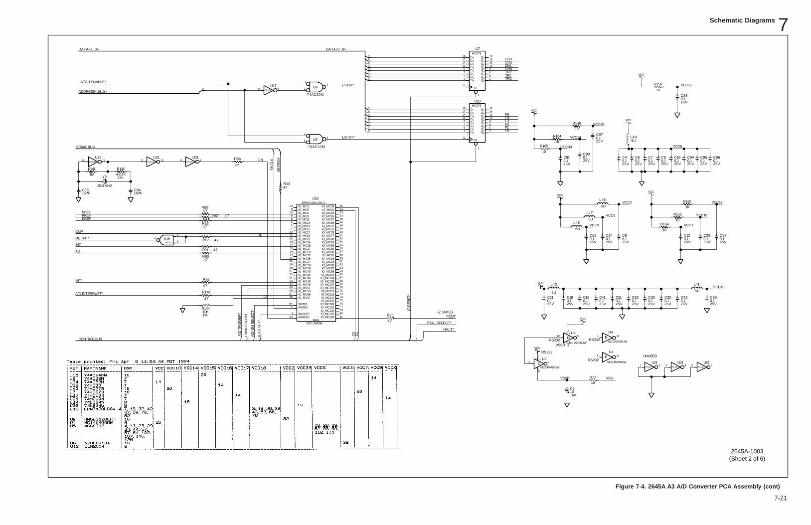
Schematic Diagrams 7
7-21
R22
10
10C5
VCC
0.1C42
0.1C20
0.1C30
0.1C6
0.1C18
0.1C41
0.1C51
0.1C52
HCU04
U9
74AC32M
0.1C50
0.1C28
0.1C19
VCC
0.1C21
47
R86
47
R92
R4847
47
R85
47R91
47R90
47R88
47R8747
R89
10.0 MHZ
Y2
15PFC84
15PFC83
R140
4.02K
R141
1M
HCU04 HCU04 HCU04
HCU04HCU04 HCU04
R14410K
U4
MC145406DW
R
U4
MC145406DW
+
D
EPM7128LC84-4
MAXSCF_IMAGE
IN/GCLKIN/GCLR
IN/OE2IN/OE1
IO_MC57IO_MC56IO_MC53IO_MC51IO_MC49IO_MC48IO_MC46IO_MC45IO_MC43IO_MC40IO_MC38IO_MC37IO_MC35IO_MC32IO_MC29IO_MC27IO_MC25IO_MC24IO_MC21IO_MC19IO_MC17IO_MC16IO_MC14IO_MC13IO_MC11IO_MC8IO_MC6IO_MC5IO_MC3
IO_MC128IO_MC126IO_MC125IO_MC123IO_MC120IO_MC118IO_MC117IO_MC115IO_MC112IO_MC109IO_MC107IO_MC105IO_MC104IO_MC101IO_MC99IO_MC97IO_MC96IO_MC94IO_MC93IO_MC91IO_MC88IO_MC86IO_MC85IO_MC83IO_MC80IO_MC77IO_MC75IO_MC73IO_MC72IO_MC69IO_MC67IO_MC65IO_MC64IO_MC61IO_MC59
R148
47
R121 47
VCC
R165
10
R164
10
0.1C91 0.1
C90
0.1C29
0.1C12
R158
10R154
10
VCC
VCC
L495U
L46
5U
0.1C16
0.1C8
0.1C7
0.1C4
L41
5U
L42
5U
L48
5U
0.1C39
R160
10
L47
5U
0.1C17
0.1C9
VCC
0.1C95
0.1C94
0.1C97
R149
10
0.1C96
VCC
R150
10
0.1C38
HC273
CL
DDDDDDD
7
6
5
4
3
2
1
0
7
6
5
4
3
2
1
0
QQQQQQQQ
D
HC273
CL
DDDDDDD
7
6
5
4
3
2
1
0
7
6
5
4
3
2
1
0
QQQQQQQQ
D
U9
74AC32M
U4
MC145406DWR
HC00
VCC
U4
MC145406DW
+
D
(2.5MHZ)
UNUSED
10
8
7
1
13412
8
5
1
116
84
83 8180797776757473717069686765646362616058575655545251504948464544
4140393736
353433
3130292827252423
2221201817161514
12111098654
2
1
U18
9 813 12 11 10
654321
9 8
3 254
7 698
13 121514
17 161918
11
1
3 254
7 698
13 121514
17 161918
11
1
65
4
32
1
65
4
NREF
25V25V25V25V25V25V25V25V
DE_INT*
A/D INTERRUPT*
CONTROL BUS
INT*
AZ
INT
DREFPREF
FOUT
FIN
HALT*
STAL SELECT*
SERIAL BUS
ADDRESS<16..0>0
25V 25V
VCC7
25V
VCC2
VCC6
VCC9
25V 25V 25V
U21 U21 U21
23
01
65
7
4
12
0
3
67
45
DATA<7..0> DATA<7..0>
LATCH ENABLE*
LS<0>*
LS<1>*
TR2
F0F1F2F3F4F5
TR0TR1
CH3CH2CH1CH0
25V 25V 25V 25V 25V 25V 25V 25V 25V 25V
VCCX
16V
VSSR VSS
U21U21U21
25V
25V
VCC15
VCC14
25V
VCC33
25V
VCC16
U16
1%
U17
U7
U10
IG R
ES
ET*
RS232
RS232
RS232VSSR
RS232
VCC10
VCC17
VCC5
1%
C1
C0
A/D
TR
IGG
ER
*
CM
ND
STR
OB
E
A/D
SM
SE
LEC
T*
SB
CLK
IG R
ES
ET*
C2
DECMP
SB
RE
CV
2645A-1003(Sheet 2 of 6)
Figure 7-4. 2645A A3 A/D Converter PCA Assembly (cont)
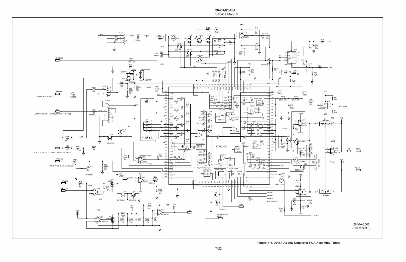
2640A/2645AService Manual
7-22
A
K27
2500PFC82
Q19
SB90041
R135
24.9K
A
100KR103
Q22
MPS6560
0.1C81
30.1KR136
.047C79
MPS6560
Q21
Q20SB90041
30.1KR137
R133
1.00K
100KR134
R102
100K
CR6BAV99
R129
10
R132
100K
A
MPS6560
Q17
A
R104
100K
R108
30.1K
A
R127
1.00K
0.1C59
18K
2K
54-4
118T
T
Z5
R1191.00K
A
33
C71
33
C72
470C65
470C64
1KR138
C732200PF
1.013K
Z6
12.25K
Z6
111.1KZ6
1.111M
Z6
47KR74
47KR97
47KR105
Q7
SB
9004
1
Q6
SB90041
A
U23
LM393DT
14K14K
54-4111TZ3
14K14K
54-4111TZ4
U29
LF357M
1K
Z7
10M
Z7
1M
100K
10K
1K
Z7
Z2
3.3K
AD706
U27
AD706
U31
AD706
U27
TP2
TP1
R125
22
A
R126
100K
A
A
R10710
R10610
47
R118
U26
AD637KD
DB
RMSOUTCHPSEL
OFFNUL
ACOMVIN
CAVDENIN
BUFIN BUFOUTVSP
VSM
LT1006
U28 W8
MC34072D
U32
MC34072D
U32
LM393DT
U23
U31
AD706
Q18
MPS6560
10C68
10
C67
2.776K
Z6
115.7
Z6
Q8
SB90041
Q23
SB90041
Z8
2.0K
14.0
K48
.336
K
R14347K
RELAY/STATUS PORT
RP1RP0
RP2RP3
RP5
RP7RP6
RP4
OSCILLATOR
G_AMP
FREQ_COMP
LO2
AGND
AG
ND
HGRD
HGRD
LGRD
LOV
LO1
IOUT
IG
S18
SGRD
IS
S46
NBIAS
HGRD
HGRD
AGND
BIAS
AGND
TCO
BIAS_AMP
AGND
BIAS
NBIAS
AC
FO
AC
FI
ACA-
HI
ACAO
ACA+
AGND
HGRD
HGRD
DCF2
HGRD
DCFO
DCFI
F_AMP
C-
HG
RD
C+
AC
R+
VD
D
VS
S
AC
R4
AC
R5
AC
R2
AC
R3
HRESET
FIN
BR+
DCA+
DCAO
DCA-
HGRD
BR-
BR1
BR2
BR3
BR4
LGRD
VDD
RESET
DGND
LGR
D
LO
G_AMP
LGRD
BR
S
SC
K
RC
V
SN
D
CS
*
SERIAL COMM
DG
ND
XO
UT
XIN
VS
S
RP
7
AC
R1
AC
R-
HG
RD
TR
HG
RD
HI2
HG
RD
HI1
VDD
V3S
V3
HGRD
SGRD
SGRD
V7
SGRD
V6S
V6
SGRD
V5S
V5
SGRD
V4S
V4
RP
6
RP
5
RP
4
RP
3
RP
2
RP1
RP
0
SGRD
V7S
LGRD
CTRI
DCLO
S1
S6
S11
S7
S2
S3
S8
S12
S13
S9
S4
S5
S10
S14
S15
S35
S24
S30
S23
S29
S22
S28
S21
S36
S37
S57B
S56B
S55B
S49
S48
S47
S45
S44
S62B
S39
S62A
S61A
S50
S43
S42S40
S41
S59B
S60BS60A
S59A
S58A
S19
DCHI
S31
S64
S20SOURCE1.2V, 3V
S27
S16
S17S65
S34
S26
S32
S33
S25
S54A
S57A
S56A S55A
S54B
S53
F_AMP
MRSTHRESET
RESET
189PFC1
VDD
SCKRCVBRS
HRESETCSSND
STALLION
S51
S52
S61B
S58B S63
S38
4.95K
Z2
R14510K
Q33
MMBT3906
R146
270
NB
C
SB90041
Q24
SB90041
Q9
R147
1.07K
A
R155
510
L52
15M
R18359.0K
A
A
R156
6.2K
180PFC98
CR15
MMBD7000
A
180PFC97
A
68PFC85
Q26
SB90041
Q25
SB90041
AA
C70
0.1
C69
0.1
0.1C78
0.1C58
VR36.0V
A
47
KR
121
47
KR
122
C76
4.3PF
R120
47K
R117
22
Q10
SSTH17
Q11
SSTH17
Q12
SSTH17
Q14
SSTH17Q15
SSTH17
SSTH17
Q16
47
KR
123
47
KR
124
Q13
SSTH17
VR2
6.0V
C75
0.1
A
A
A
A
BAV99CR5
A
3.45KR128
C80
0.1
1.0
C66
A
K25
R139
100K
R131
10
R130
100KK26
R111
1K0.1C57
R110
1K
VIATP5
TP6TP7 VIAVIA
54
-40
98
T
R
(FRDY)
(30VDC, 300VDC HI-SENSE, OHMS-HI-SOURCE)
(OHMS, .3VDC & 3VDC)
S
R
S
(30VDC, 300VDC-LO-SENSE, OHMS-LO-SOURCE)
(.3VDC, 3VDC, OHMS-LO-SENSE)
TP4VIA
R
S
10099989796959493929190898887868584838281
80
79
78
77
76
75
74
73
72
71
70
69
68
67
66
65
64
63
62
61
60
59
58
57
56
55
54
53
52
51
50 49 48 47 46 45 44 43 42 41 40 39 38 37 36 35 34 33 32 31
30
29
28
27
26
25
24
23
22
21
20
19
18
17
16
15
14
13
12
11
10
9
8
7
6
5
4
3
2
1
U30
3 21
4 3
87
97
32
1
74
75
76
1412
10
1311
9
8
64
7
53
8
64
1311
9
8
64
1311
9
8
4
3
21
8
76
5
4
8
7
6
5
4
3
2
1
8
4
3
21
8
76
5
4
7
6
4
3
2
87
65
4
3
21
11109
8
4
3
21
8
4
3
21
8
76
5
4
8
76
5
4
14
13
11
10
9
876543
1
3
2
1
3
2
1
3
2
1
4
3
2
1
2%50V
RGRD
1%
VCLAMP
VCLAMP
3W
1/4W
CH24CH24
1000V
CH24
VDD
1%
VDD
VSS
VDD
VSS
1%
OTC
VDD
1%
1%
VDD
VSS
1%
OTC_EN
OTCCLK
3W
LO
RJ SENSE
HI
FUSIBLE
VSS
VAC-
VDDB
AD HI
AD LO
RIVSSB
FUSIBLE
CH24
CH24
1%
1%
VAC-
VAC+
6V6V
25V
VAC+
ACR5
VAC- 25V
VDD
50V VAC-
VSS
1%
RI
VDD
VSS
1%
1%1%
160V
100V
+3.45V
STAL INTERRUPT
25V1%
HI SENSE
LO SENSE
250V
16V
VAC+
10V
10V
160V
160V
VDD
VDD
25V
SB RECV
STAL SELECT*
SB XMIT
SB CLK
DISCHARGE
1%
VDD
1%
25V
VSS
FOUT
VSS
VDDB
IG RESET*
1%
16V
VSSB
VDDVDD
VSS
50V
1%
LOW
VSSB
VDDB
1/4W
50V2%
50V2%
2640A-1003(Sheet 3 of 6)
Figure 7-4. 2645A A3 A/D Converter PCA Assembly (cont)
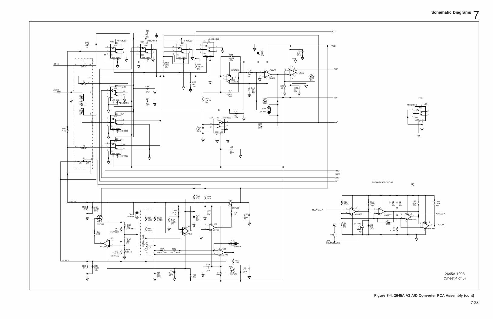
Schematic Diagrams 7
7-23
10KR4
0.1C3
30.1KR16
U3
LM393DT
100KR15
U3LM393DT
R61
1.07K
U11LT1016C
R2
470K
470KR3
0.1C2
U1
LM393DT
BAV99
CR2
BAV99
CR3
U12
AD706
A
91K
R93
R8210K
AD822U19
AD822U19
Q4SST109
A
CR4BAV99
A
R7128.7K
A
A
A0.1C22
0.1C32
0.1
C55
0.1
C54
A
R51.07K
VCC
14K 14K
Z1
44.97K
Z1
44
.97
K10
0K6.
6K
Z1
89.97K
Z1
38.27K
Z1
74HC4053U24
VCC
GNDVEE
INH
R9929.4K
74HC4053
U24VCC
GNDVEEINH
74HC4053
U24VCC
GNDVEE
INH
OP295
U20
OP295
U20
R9810K
R9510K
0.01C25
A
R211.5K0.1
C1
10C45
10C46
A
R9445.3K
A
74HC4053U22
VCC
GNDVEEINH
A
A
0.1C23
0.1C24
R81200
R70200
R72200
R101
1.07K
74HC4053U25
VCC
GNDVEE
INH
74HC4053 U25
VCC
GNDVEE
INH
Q1
2N7002VCC
W5
74HC4053
U22VCC
GNDVEE
INH
74HC4053U22
VCC
GNDVEE
INH
74HC4053U25VCC
GND VEE
INH
R83402
LM393DT
U1
A
A
0.1C53
A
A
0.1
C63
0.1
C62
0.1
C61
R14247K
A
26
40
A-4
50
1
Q5
R63SEL2
R64SEL1
R1004.02K
R68200
A
R692K
0.1C34
R84200A
0.1
C49
U12
AD706
SST175
Q3
0.01
C48
A
R677.5K
0.001C35
R651.07K
R66200
0.1C47
A
A
A
Q2
SST109
0.1C36
A
R73200
R962K
A
0.001C56
AA
R80
1000.47C60
A
R7726.1K
3.3PF
C43
R79
110K
AA
R6210
1500PF
C44
R78
10K
A
A
(FROM SHEET 1)
BREAK-RESET CIRCUIT
C
A
8
4
3
21
8
76
5
4
8
7
6
5
4
3
2
1
8
4
3
21
8
76
5
4
8
4
3
21
8
76
5
4
14
13
117
12
6
54
108
3
21
8
76
5
4
8
4
3
21
8
4
3
21
8
76
5
4
16
1413
12
11
8 7
6
16
15
10
87
62
1
16
1413
12
11
87
6
16
9
87
65
43
16
15
10
87
62
1
16
9
87
65
43
16
15
10
87
62
1
16
1413
12
11
87
6
16
9
87
65
43
1%
25V
16V
50V
25V
25V
50V
25V
25V
50V
50PPM/C
50V
50V1%
1%
1% 25V
25V 25V
IG RESET*
1%1%
1%
1%
RECV DATA
PREF
NREF
DREF
INT
AZ
VSS
CMP
INT*
VDD
1%
25V16V
100V
1%1%
25V
AD HI
1%
AD LO
+3.45V
1%
25V
50V
1%
25V
HALT*
25V 25V
25V
-3.45V
25PPM/C
25PPM/C 25V
VBOOT
25V
VDD
VSS
LEADED LEADED
2645A-1003(Sheet 4 of 6)
Figure 7-4. 2645A A3 A/D Converter PCA Assembly (cont)
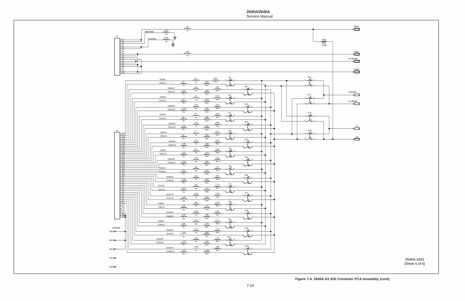
2640A/2645AService Manual
7-24
L39
5U
A
A
L38
5U
L18
5U
L36
5U
R116
270
K20
K3
K10
L16
5U
K19
K9
K18
K17
K16
K8
K7
K6
K15
K24
L19
5U
K23
K22
K21
K11
K1
K14
K5
K2
K12
K13
L37
5U
K4
J2
L17
5U
L35
5U
WP1
WP3
L43
5U
L45
5U
L51
5U
L44
5U
L100
33U
L99
33U
L80
33U
L79
33U
L98
33U
L97
33U
L78
33U
L77
33U
L96
33U
L95
33U
L76
33U
L75
33U
L94
33U
L93
33U
L73
33UL74
33U
L92
33U
L91
33U
L72
33U
L85
33U
L67
33U
L87
33U
L69
33U
L89
33U
L71
33U
L90
33U
L70
33U
L88
33U
L68
33U
L86
33U
L66
33U
L63
33U
L83
33U
L65
33U
L84
33U
L64
33U
L82
33U
L81
33U
L62
33U
L61
33U
WP4
WP2
WP5
J1
L34
5U
L14
5U
L32
5U
L12
5U
L15
5U
L33
5U
L13
5U
L31
5U
L30
5U
L10
5U
L28
5U
L8
5U
L11
5U
L29
5U
L9
5U
L27
5U
L26
5U
L6
5U
L24
5U
L4
5U
L25
5U
L7
5U
L40
5U
L5
5U
L23
5U
L3
5U
L22
5U
L2
5UL21
5U
L1
5U
L20
5U
CH20 LO
CH20 HI
CH10 LO
CH10 HI
CH19 LO
CH19 HI
CH9 LO
CH9 HI
CH18 LO
CH18 HI
CH8 LO
CH8 HI
CH17 LO
CH17 HI
CH7 LO
CH7 HI
CH16 LO
CH16 HI
CH6 LO
CH6 HI
CH15 LO
CH15 HI
CH5 LO
CH5 HI
CH14 LO
CH14 HI
CH4 LO
CH4 HI
CH13 LO
CH13 HI
CH3 LO
CH3 HI
CH12 LO
CH12 HI
CH2 LO
CH2 HI
CH11 LO
CH11 HI
CH1 LO
CH1 HI
CHASSIS
65
87
65
87
65
87
65
87
65
87
65
87
65
87
65
87
65
87
65
87
65
87
65
87
65
87
65
87
65
87
65
87
65
87
65
87
65
87
65
87
65
87
65
87
65
87
65
87
B26
A31
A27
B28
C27A29C29A23C23A25
C21A19A21C25
B30
B20
C17
B18
C19A17
C15
B12B14B16A15
B32
A11
B10C13A13
C9C11A9B8B6C7
C31
A7C5C3
A5B4
C1
B22A1
B2A3
B24
A10B9A9B8A8B7A7B6A6B5A5B4A4B3A3
A2
A1
B10
B2
B1
LO SENSE
SHLD
RJ RTRN
REF RTRN
VDD
RJ SENSE
RGRD
HI SENSE
HI
LO
1/4W
2645A-1003(Sheet 5 of 6)
Figure 7-4. 2645A A3 A/D Converter PCA Assembly (cont)
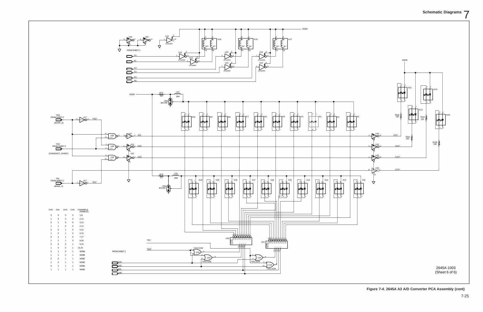
Schematic Diagrams 7
7-25
K3 K2
K11K12K13K14K15K16K17K18K19K20
ULN2004
U13
HCU04
HCU04
HC00
HC00
HC00
I
Y Y Y Y Y Y Y Y013456789
LS14
5D
EC
OD
ER
3
2
YY
I I I2 1 0
U34
74AC32M
U34
74AC32M
U34
74AC32M
U34
74AC32M
AC240
AC240
AC240
AC240
AC240
AC240
AC240 AC240
BAV99CR9
L52
15M
L50
15M
BAV99CR8
R76
33
R75
33
ULN2004
U13ULN2004
U13
K26
SETRST
I
Y Y Y Y Y Y Y Y013456789
LS14
5D
EC
OD
ER
3
2
YY
I I I2 1 0
ULN2004
U13
ULN2004
U13
ULN2004
U13
ULN2004
U13
K25
SETRST
K27
SETRST
R112150
R113150
R114150
R138150
HCU04
K24
K23
K22
K21
K1K10 K9 K8 K7 K6 K5 K4
FROM SHEET 2
(OHMS/NOT_OHMS*)
(BANK_1)
(BANK_0)
6,16
5,15
4,14
3,13
2,12
1,11
ENABLEDCHANNELS
0
0
0
0
0
0
CH3
1
1
0
0
0
CH1 CH2
0
0
1
1
0
0
0
1
0
1
0
1
0
CH0
0 7,17011
NONE
NONE
NONE
NONE
NONE
NONE
10,20
9,19
8,18
1
1
1
1
1
1
1
1
01 1
0 0
00
1 0
01
1
1
10
10
1
1
1
0
1
0
0
1
1
0
1
FROM SHEET 2
FROM SHEET 2
FROM SHEET 2
FROM SHEET 2
15
9
2
13
9
4
11
9
6
10
9
7
14
9
3
12
9
5
16
9
1
1615
2 1
1615
2 1
1615
2 1
4
3
2
1
4
3
2
1
4
3
2
1
4
3
2
1
4
3
2
1
4
3
2
1
4
3
2
1
4
3
2
1
4
3
2
1
4
3
2
1
4
3
2
1
4
3
2
1
4
3
2
1
4
3
2
1
4
3
2
1
4
3
2
1
4
3
2
1
4
3
2
1
4
3
2
1
4
3
2
1
4
3
2
1
4
3
2
1
4
3
2
1
4
3
2
1
15141312
11 10 9 7 6 5 4 3 2 1
15141312
11 10 9 7 6 5 4 3 2 1
13 12
21
65
32
1
10
98
13
1211
65
4
10
98
13
1211
32
1
128
1
U15
19
11 9U15
19
13 7
U1519
17 3U15
164
1
U15
146
1
U15
182
1
U15
19
15 5U15
VDDR
U14
U33
VDDR
CH0
U17
U17
F5
F4
TR0
TR1
F3
F2
F1
F0
TR2
TR0*
TR1*
U17
K24*
K23*
K22*
K21*K21
CH1
CH2
CH3
TR1*
TR0*
K23
K22
U16
U16
U16
VDDR
2645A-1003(Sheet 6 of 6)
Figure 7-4. 2645A A3 A/D Converter PCA Assembly (cont)
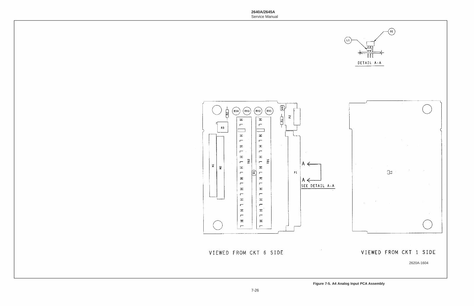
2640A/2645AService Manual
7-26
Figure 7-5. A4 Analog Input PCA Assembly
2620A-1604
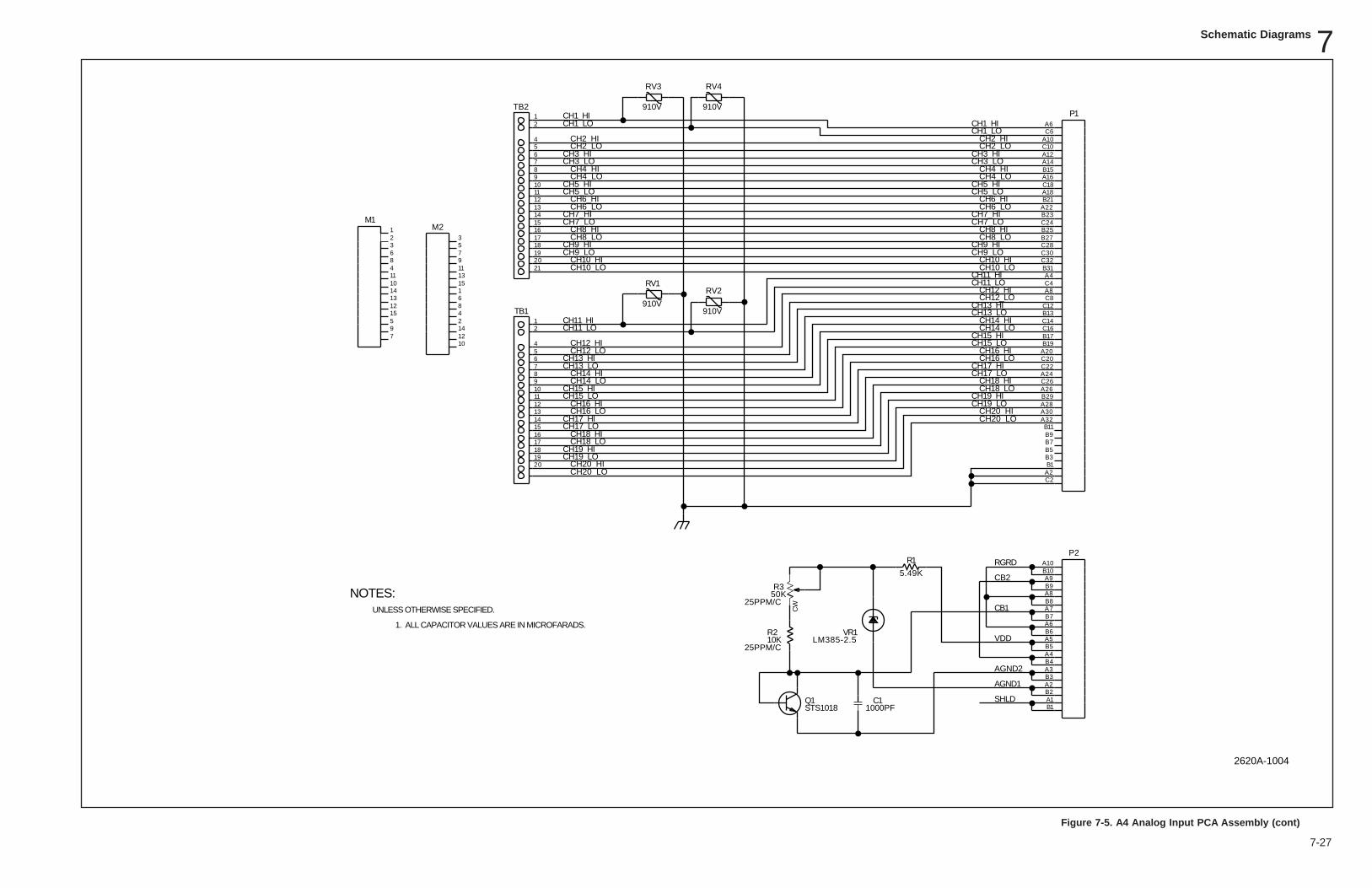
Schematic Diagrams 7
7-27
M1
M2
P2
P1
RV1
910V
RV2
910V
RV4
910V
RV3
910VTB2
TB1
10KR2
R1
5.49K
Q1STS1018 1000PF
C1
VR1LM385-2.5
CW
50KR3
UNLESS OTHERWISE SPECIFIED.
NOTES:
1. ALL CAPACITOR VALUES ARE IN MICROFARADS.
A10C10A12A14B15
C18A18B21
A16
A22B23C24B25B27C28C30C32B31A4C4A8C8
C12B13C14C16B17B19
A20C20C22A24C26A26B29A28A30A32B11
A6
B9B7
B3B5
B1A2C2
C6
2019181716151413121110987654
21
212019181716151413121110987654
21
A1B2A2B3A3B4A4B5A5B6A6B7A7B8A8B9A9
B10A10
B1
3
4
68
1011
121314
155
79
35791113151
24
68
101214
12
RGRD
CB2
CB1
CH20_LO
CH20_LO
CH20_HI
CH20_HI
CH19_LO
CH19_LO
CH19_HI
CH19_HI
CH18_LO
CH18_LO
CH18_HI
CH18_HI
CH17_LO
CH17_LO
CH17_HI
CH17_HI
CH16_LO
CH16_LO
CH16_HI
CH16_HI
CH15_HI
CH15_LO
CH15_LO
CH15_HICH14_LO
CH14_LO
CH13_LO
CH13_LO
CH14_HI
CH14_HI
CH13_HI
CH13_HI
CH12_LO
CH12_LO
CH12_HI
CH12_HICH11_LO
CH11_HI
CH11_HICH10_LO CH10_LOCH10_HI CH10_HI
CH9_LO CH9_LOCH9_HI CH9_HI
CH8_LO CH8_LO
CH7_LO CH7_LOCH8_HI CH8_HI
CH7_HI CH7_HICH6_LO CH6_LOCH6_HI CH6_HI
CH5_LO CH5_LOCH5_HI CH5_HI
CH4_LO CH4_LOCH4_HI CH4_HI
CH3_LO CH3_LOCH3_HI CH3_HI
CH2_LO CH2_LOCH2_HI CH2_HI
CH1_HI
CH1_LOCH1_HI
SHLD
25PPM/C
25PPM/C
AGND1
AGND2
VDD
CH11_LO
CH1_LO
2620A-1004
Figure 7-5. A4 Analog Input PCA Assembly (cont)

2640A/2645AService Manual
7-28
Related Documents


![CERTIFICATE OF CALIBRATION - Fluke Caldownload.flukecal.com/pub/literature/9010444_ENG_A_W[1].pdf · AC Voltmeter Fluke 5790A 9380036 C1/778B 29 May 2011 ... CERTIFICATE OF CALIBRATION](https://static.cupdf.com/doc/110x72/5bdcd85509d3f2321d8c1ad2/certificate-of-calibration-fluke-1pdf-ac-voltmeter-fluke-5790a-9380036-c1778b.jpg)


