2.4 GHz ANTENNA INTEGRATED SOLAR PV CELL by SERKAN ER by Associate Prof. KORKUT YEĞİN (Thesis supervisor) ENGINEERING PROJECT REPORT Yeditepe University Faculty of Engineering and Architecture Department of Electrical and Electronics Engineering Istanbul, 2009

Welcome message from author
This document is posted to help you gain knowledge. Please leave a comment to let me know what you think about it! Share it to your friends and learn new things together.
Transcript

2.4 GHz ANTENNA INTEGRATED SOLAR PV CELL
by
SERKAN ER
by
Associate Prof. KORKUT YEĞİN
(Thesis supervisor)
ENGINEERING PROJECT REPORT
Yeditepe University
Faculty of Engineering and Architecture
Department of Electrical and Electronics Engineering
Istanbul, 2009

1
ACKNOWLEDGMENTS I would like to acknowledge and extend my sincere gratitude to the following persons who
made the completion of this project possible:
• Associate Prof. Korkut Yeğin, for his encouragement and support,
• Ayberk Bağcı, Genetlab for providing assistance on wireless modules
• Gökmen Işık and Murat Bilgiç for their patience and assistance,
• Tuğba Haykır and Safa Ergin for their help and inspiration,
• Above all, to my family.

2
ABSTRACT
In this work, a novel 2.4 GHz ISM band microstrip patch antenna integrated with
photovoltaic (PV) solar cell is designed, built and measured. Solar PV cell serves as a
ground plane for the microstrip antenna. The antenna is a part of a wireless node and
transceiver circuit which performs sensing and communication functions. An existing
wireless node is used and hooked to the antenna to measure certain performance metrics of
the wireless node. The antenna is designed with a 3D electromagnetic solver.
Measurements of the prototyped antenna exhibit very good agreement with the simulation
results. The DC converter circuit for the solar cell is also designed and built. PV cell
current-voltage measurements are also performed. With this system, the energy provided
by the solar cell is enough to operate a standalone wireless node without any external
power source.

3
ÖZET Bu çalışmada 2.4 GHz lisanssız frekans bandında çalışan, fotovoltaik güneş hücresi
üzerinde yeni bir mikroşerit yama anten tasarlandı, prototipi yapıldı ve ölçümleri
gerçeklendi. Güneş hücresi mikroşerit anten için toprak görevi gördü. Anten, iletişim ve
ölçme işlemlerini gerçeleştiren kablosuz duyarganın alıcı/verici devresine bağlı
çalışmaktadır. Varolan kablosuz bir duyarga kullanılarak, anten ve kablosuz duyarga
performans parametreleri ölçülmüştür. Anten 3 boyutlu elektromagnetik benzetim program
kullanılarak tasarlanmıştır. Prototipi yapılan antenin ölçüm sonuçları benzetim sonuçları ile
örtüşmektedir. Güneş hücresinin DC çevirici devresi de tasarlanıp, gerçeklenmiştir.
Fotovoltaik hücrenin akım-gerilim ölçümleri yapılarak güç eğrisi de çıkartılmıştır. Bu
sistemle, güneş hücresinden gelen enerji kablosuz bir duyargayı, pil gibi harici bir güç
kaynağı olmaksızın çalıştırabileceği gösterilmiştir.

4
Table of Contents
1. INTRODUCTION ........................................................................................................... 10
2. BATTERY CHARGING WITH SOLAR PV CELL ...................................................... 11
2.1 Solar PV Cells ............................................................................................................ 11
2.2 Rechargeable Ni-MH Batteries .................................................................................. 12
2.2.1 Charging of Ni-MH Batteries ............................................................................. 12
2.2.2 Comparison with Other Battery Types ............................................................... 12
2.3 Buck Converter .......................................................................................................... 12
2.3.1 Explanation of Buck Converter Circuit with LM2574 ....................................... 13
2.3.2 Measurements of Buck Converter Circuit .......................................................... 15
3. OVERVIEW OF MICROSTRIP PATCH ANTENNA THEORY ................................. 18
3.1 Introduction to Microstrip Patch Antenna .................................................................. 18
3.2 Basic Patch Antenna Shapes and Geometries ............................................................ 19
3.3 Basic Antenna Parameters .......................................................................................... 19
3.3.1 Directivity ........................................................................................................... 19
3.3.2 Input Impedance ................................................................................................. 20
3.3.3 Voltage Standing Wave Ratio (VSWR) ............................................................. 21
3.3.4 Antenna Efficiency ............................................................................................. 22
3.3.5 Antenna Gain ...................................................................................................... 22
3.3.6 Bandwidth……………………………………………………………………...23
4. MICROSTRIP PATCH ANTENNA DESIGN ............................................................... 24
4.1 Efficiency, Impedance and VSWR ............................................................................ 26
4.2 Parameters of the Antenna ......................................................................................... 29
4.3 Measurements……………………………………………………………………….30

5
4.3.1 Grounding The Antenna and Wireless Module………………………………...30
4.3.2 Determination of VSWR……………………………………………………….31
4.3.3 Measurement of Antenna Power by using Spectrum Analyser………………...33
5. CONCLUSION ................................................................................................................ 36
6. REFERENCES………………………………………………………………………….37

6
LIST OF FIGURES
Figure 2.1 Our PV cell with the antenna……………………………….…………..11
Figure 2.2. Adjustable Output Voltage Version of LM2574…………….................13
Figure 2.3. The charger circuit………………………………...................................14
Figure 2.5. Charging Circuit while the batteries at about saturation......................... 17
Figure 3.1. Structure of a microstrip patch antenna………………………………...19
Figure 3.2. Equivalent circuit of transmitting antenna……………………………...21
Figure 4.1 Side view of the antenna………………………………………………..24
Figure 4.2 Geometry of the antenna………………………………………………..25
Figure 4.3 Feed line geometry………..…………………………………………….25
Figure 4.4 Side view of the antenna with coaxial probe feed……………………...26
Figure 4.5 Representation of the antenna in EAGLE PCB drawing program…..…26
Figure 4.6 Efficiency of antenna in FEKO……………..………………………….27
Figure 4.7 Real impedance of antenna in FEKO…………..………………………27
Figure 4.8 Imaginary impedance of antenna in FEKO……………………….…....28
Figure 4.9 VSWR of antenna between small frequency band……..………………28
Figure 4.10 Three dimensional Gain of antenna at 2.45 GHz………………………29
Figure 4.11 Gain graph of the antenna……..………………………………………..30
Figure 4.12 Backside of the module ……………………..………………………….30
Figure 4.13 Wireless module...…………………………..…………………………..30
Figure 4.14 Scene of the antenna while measuring VSWR………………..………..31
Figure 4.15 VSWR measured by network analyzer ……….………………………..32

7
Figure 4.16 Placements of the antennas…………………..…………………………33
Figure 4.17 VSWR Graphs of The Antenna - Section 1….………………..………..33
Figure 4.18 VSWR Graphs of The Antenna - Section 2…………….……..………..34
Figure 4.19 VSWR Graphs of The Antenna - Section 3………….………..………..35
Figure 5.1 The microstrip patch antenna integrated PV cell with charger circuit…36

8
LIST OF TABLES
Table 2.1. The result table of power measurement of PV cell.................................12
Table 2.2. Discharging Values..................................................................................15
Table 2.3. Charging Values......................................................................................16
Table 4.1 Summary of microstrip patch antenna at 2.45GHz……........................29
Table 4.2 Comparison table between desired and simulated values......................32
Table 4.3 Summary of measurement of antenna directivity..................................35

9
LIST OF SYMBOLS
NiMH: Nickel-metal hydride
NiCd: Nickel cadmium
mAh: mili ampere hour
Γ: reflection coefficient

10
1. INTRODUCTION An increasingly large number of electronic devices are now portable. Many
advances allow for portable devices, including smaller and lighter electronics, electronics
which use less power, improved batteries and power supplies, etc. These technological
advances allow many types of electronic devices to operate without requiring wired
connection to communications networks or power grids [1].
Recently, communication systems integrated with photovoltaic technology for low
cost and stand alone applications received much interest. The photovoltaic systems of
power generation when combined with communications systems can provide compact and
reliable autonomous communication systems for many applications. A stand alone remote
base station is one such application where PV technology can be used. But these devices
often involve the use of separate solar cells and antennas, which necessitate a compromise
in the utilization of the limited surface available. Integrating the base station antennas into
photovoltaic solar cells can provide compact and reliable solution [5].
The device in this project operates without connection to an outside power source
for extended periods of time. A solar cell is desirable for facilitating operation without an
outside source of power. Batteries are often utilized, but the batteries capable of operating
the device for extended periods of time (such as weeks or months) are typically much too
large to be conveniently included in the device. Thus, solar panels are often used to power
devices. Solar panels are often used in combination with batteries to provide energy to the
device and to charge the batteries during the day and thereby extend the time period for
which the device may operate. If the solar panel is large enough, the device may operate
indefinitely. It is thus often desirable to have a solar panel which is large enough to meet
the energy requirements of the device.
It is free to use 2.4 GHz ISM band is abundantly used for WLAN, portable
electronics communication and sensor networks. A communication antenna and a
tranceiver system are usually isolated from DC supply such as battery or PV cell. Here,
Our goal is to integrate communication/sensor antenna with PV cell and utilize PV cell as a
back-up power source.

11
2. BATTERY CHARGING WITH SOLAR PV CELL Stand alone applications like environmental monitoring systems or satellite systems
need a net-independent power supply which is preferably realizable by photovoltaics, an
advanced technology distinguished by reliability, longevity and eco-friendliness [6].
In this project, we have two 1.2V rechargeable batteries to feed the module of
microstrip patch antenna. One of our goals is to charge these batteries with solar energy.
2.1 Solar PV Cells
A solar cell or a photovoltaic cell is a device that converts photons from the sun’s
radiation into electricity. In general, a solar cell that includes both solar and non solar
sources of light is termed as photovoltaic cell.
The development of the thin amorphous silicon on polymer substrate solar cell
technology made it possible to easily cut and fit the solar cells to various shapes such as
slot antennas, leading to optimized use of the available area, without affecting the radiating
characteristics of the antenna [3].
Figure 2.1 Our PV cell with the antenna
Our PV cell integrated with the antenna serves as a back-up power source and also
as a ground plane. We had a measurement of PV cell in a sunny day to understand how
much power PV cell can produce with different resistors which are 1, 10, 15, 100, 510,
1kΩ.
The table below shows the data from the measurement. The measurement is made
at 3 o’clock, so the position of the sun is not 90° to the earth. We rotated PV cell to the
sun. Here you can see the results:

12
Table 2.1 The result table of power measurement of PV cell
The data in the red tone show the maximum power produced by PV cell. When PV cell is
horizontal position, the maximum power is 405 mW and in towards sun position, the
maximum power is 560 mW. When I got these results, I got really excited. Because the
produced power is enough to charge the batteries in the project.
2.2 Rechargeable Batteries
2.2.1 Charging of Ni-MH Batteries
The charging voltage is in the range of 1.4–1.6 V/cell. A fully charged cell
measures 1.35–1.4 V (unloaded), and supplies a nominal average 1.2 V/cell during
discharge, down to about 1.0–1.1 V/cell (further discharge may cause permanent damage).
In general, a constant-voltage charging method cannot be used for automatic charging.
When fast-charging, it is advisable to charge the NiMH cells with a smart battery charger
to avoid overcharging, which can damage cells and cause dangerous conditions. A NiCd
charger should not be used as an automatic substitute for a NiMH charger [2].
2.2.2 Comparison with Other Battery Types
NiMH cells are not expensive, and the voltage and performance is similar to
primary alkaline cells in those sizes; they can be substituted for most purposes. The ability
to recharge hundreds of times can save money and resources.
They accept both higher charge and discharge rates and micro-cycles thus enabling
applications which were previously not practical [5].
2.3 Buck Converter
If you need an output voltage that's smaller than the input voltage, then the Buck
Converter is your choice. The simplest way to reduce a DC voltage is to use a voltage

13
divider circuit, but voltage dividers waste energy, since they operate by bleeding off excess
power as heat; also, output voltage isn't regulated (varies with input voltage). A buck
converter, on the other hand, can be remarkably efficient (easily up to 95% for integrated
circuits) and self-regulating.
2.3.1 Explanation of Buck Converter Circuit with LM2574
Since the LM2574 converter is a switch–mode power supply, its efficiency is
significantly higher in comparison with popular three–terminal linear regulators. In most
cases, the power dissipated by the LM2574 regulator is so low, that the copper traces on
the printed circuit board are normally the only heatsink needed and no additional
heatsinking is required.
Figure 2.2 Adjustable output voltage version of LM2574 [7]
Vin pin is the positive input supply for the LM2574 step–down switching regulator.
In order to minimize voltage transients and to supply the switching currents needed by the
regulator, a suitable input bypass capacitor must be present (Cin in Figure 2.3). Cin is to
prevent large voltage transients from appearing at the input and for stable operation of the
converter, an aluminum or tantalum electrolytic bypass capacitor is needed between the
input pin +Vin and ground pin “Gnd”.
Feedback pin senses regulated output voltage to complete the feedback loop. The
signal is divided by the internal resistor divider network R2, R1 and applied to the non–
inverting input of the internal error amplifier. In the Adjustable version of the LM2574
switching regulator, this pin is the direct input of the error amplifier and the resistor
network R2, R1 is connected externally to allow programming of the output voltage.

14
ON/OFF pin allows the switching regulator circuit to be shut down using logic
level signals, thus dropping the total input supply current to approximately 80 mA. The
input threshold voltage is typically 1.5 V. Applying a voltage above this value (up to +Vin)
shuts the regulator off. If the voltage applied to this pin is lower than 1.5 V or if this pin is
left open, the regulator will be in the “on” condition.
Cout is important component, since the LM2574 is a forward–mode switching
regulator with voltage mode control; its open loop 2–pole–1–zero frequency characteristic
has the dominant pole–pair determined by the output capacitor and inductor values. For
stable operation and an acceptable ripple voltage, (approximately 1% of the output voltage)
a value of 220 µF is suitable.
Catch diode (D1) must be located close to the LM2574 using short leads, The
LM2574 is a step–down buck converter, and it requires a fast diode to provide a return
path for the inductor current when the switch turns off.
Finally we can get the desired value by changing R2/R1 ratio. So we settle a
potentiometer instead of two separate resistors.
The realized circuit is here. We used two extra capacitors which are both 100 nF for
low pass filter in input and output and also used a potentiometer instead of using two
separate resistors as R1 and R2.
Figure 2.3 The charger circuit
Extra capacitors for low pass filter (100 nF)
Potentiometer for R1/R2 ratio

15
2.3.2 Measurements of Buck Converter Circuit
It was tested that whether our circuit charges the batteries or not. First, the batteries
were discharged with 10Ω (5W) resistance connected by two 1.2V Ni-MH rechargeable
batteries1 and the values were recorded as given in the below:
Table 2.2 Discharging values
Current
(mA)
Time Current
(mA)
Time
193 11:55 13 14:05
132 12:41 10 14:22
86 12:57 8.4 14:31
72 13:12 7.6 14:54
42 13:21 6.3 15:09
26 13:50 5.5 15:30
This graph shows the discharging current values taken after a certain time intervals.
In the beginning, the flowing current is nearly 200 mA and after 3.5 hours, the batteries
discharged.
1 Before that time the batteries were not fully charged.

16
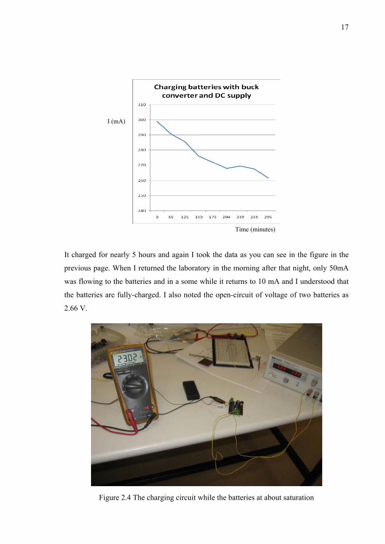
Then, to determine whether our circuit charges the batteries or not, output of the
circuit was connected to the batteries and input is connected a DC source 5V and 200
mAmax. The current values are tested as below2:
Table 2.3 Charging values
Current
(mA)
Time Current
(mA)
Time
299 18:05 267.7 22:20
290.6 19:10 261.7 23:00
285.5 20:10 52 14:05
276 20:35 38 14:40
272 21:00 32.3 15:15
268 21:29 23 15:45
269.6 22:04 18 16:10
2 Charging test processed between two time intervals which are from 6:05 to 23:00 and from 2:00 to 16:10.
I (mA)
Time (minutes)
Time (minutes)
17
It charged for nearly 5 hours and again I took the data as you can see in the figure in the
previous page. When I returned the laboratory in the morning after that night, only 50mA
was flowing to the batteries and in a some while it returns to 10 mA and I understood that
the batteries are fully-charged. I also noted the open-circuit of voltage of two batteries as
2.66 V.
Figure 2.4 The charging circuit while the batteries at about saturation
I (mA)
Time (minutes)
18
3. OVERVIEW OF MICROSTRIP PATCH ANTENNA THEORY
3.1 Introduction to Microstrip Patch Antennas
Size miniaturization of microstrip patch antenna is increasingly essential in many
practical applications, such as mobile cellular handsets, cordless phones, direct broadcast
satellites (DBS), wireless local area networks (WLAN), global position satellites (GPS)
and other next-generation wireless terminals.
Applications in present-day mobile communication systems usually require smaller
antenna size in order to meet the miniaturization requirements of mobile units. Thus, size
reduction is becoming major design considerations for practical applications of microstrip
antennas. For this reason, studies to achieve compact microstrip antennas have greatly
increased. Much significant progress in the design of compact microstrip antennas has
been reported over the past several years.
The antenna physical sizes are an important factor in the design process owing to
the miniaturization of the modern mobile terminals. Any technique to miniaturize the sizes
of the microstrip patch antenna has received much attention. Electrical requirements for
these mobile antennas are sufficient bandwidth, high efficiency, impedance matching,
omni-directional radiation patterns, and minimum degradation by the presence of near
objects, etc.
In general, the size miniaturization of the normal microstrip patch antenna has been
accomplished by loading, which can take various forms, namely;
i. Use of high dielectric constant substrates
ii. Modification of the basic patch shapes;
iii. Use of short circuits, shorting-pins or shorting-posts; and
iv. A combination of the above techniques.
Employing high dielectric constant substrates is the simplest solution, but it
exhibits narrow bandwidth, high loss and poor efficiency due to surface wave excitation.
Modification of the basic patch shapes allows substantial size reduction; however, some of
these shapes will cause the inefficient use of the available areas. In contrast, shorting posts,

19
which were regarded as a more efficient technique, were used in different arrangements to
reduce the overall dimensions of the microstrip patch antenna.
3.2 Basic Patch Antenna Shapes and Geometries
In its most basic form, a microstrip patch antenna consists of a radiating patch on
one side of a dielectric substrate, which has a ground plane on the other side as shown in
Figure 3.1.
Figure 3.1 Structure of a microstrip patch antenna [8]
The patch is generally made of conducting material such as copper or gold and can
take any possible shape. The radiating patch and the feed lines are usually photo etched on
the dielectric substrate [8].
3.3 Basic Antenna Parameters
An antenna is a device that converts a guided electromagnetic wave on a transmission line
to a plane wave propagating in free space. Thus, one side of an antenna appears as an
electrical circuit element, while the other side provides an interface with a propagating
plane wave. Antennas are inherently bi-directional, they can be used for both transmit and
receive functions [4].
3.3.1 Directivity
The directivity of an antenna has been defined by as “the ratio of the radiation
intensity in a given direction from the antenna to the radiation intensity averaged over all
directions”. In other words, the directivity of a nonisotropic source is equal to the ratio of
its radiation intensity in a given direction, over that of an isotropic source.

20
D= U/Ui = 4πU/P (3.1)
where D is the directivity of the antenna, U is the radiation intensity of the antenna, Ui is
the radiation intensity of an isotropic source, and P is the total power radiated.
Sometimes, the direction of the directivity is not specified. In this case, the
direction of the maximum radiation intensity is implied and the maximum directivity is
given by as:
Dmax= Umax/Ui = 4πUmax (3.2)
where Dmax is the maximum directivity, Umax is the maximum radiation intensity.
3.3.2 Input Impedance
The input impedance of an antenna is defined by as “the impedance presented by an
antenna at its terminals or the ratio of the voltage to the current at the pair of terminals or
the ratio of the appropriate components of the electric to magnetic fields at a point”. Hence
the impedance of the antenna can be written as:
Zin=Rin+jXin (3.3)
where Zin is the antenna impedance at the terminals, Rin is the antenna resistance at the
terminals, Xin is the antenna reactance at the terminals.
The imaginary part, Xin of the input impedance represents the power stored in the
near field of the antenna. The resistive part, Rin of the input impedance consists of two
components, the radiation resistance Rr and the loss resistance RL. The power associated
with the radiation resistance is the power actually radiated by the antenna, while the power
dissipated in the loss resistance is lost as heat in the antenna itself due to dielectric or
conducting losses.

21
3.3.3 Voltage Standing Wave Ratio (VSWR)
Figure 3.2 Equivalent circuit of transmitting antenna [9]
In order for the antenna to operate efficiently, maximum transfer of power must
take place between the transmitter and the antenna. Maximum power transfer can take
place only when the impedance of the antenna (Zin) is matched to that of the transmitter
(Zs).
If the condition for matching is not satisfied, then some of the power maybe
reflected back and this leads to the creation of standing waves, which can be characterized
by a parameter called as the Voltage Standing Wave Ratio (VSWR). The VSWR can be
expressed as:
VSWR=(Vmax/Vmin)=(1+ Γ)/ (1- Γ) (3.4)
where Γ
Γ =Vr/Vi=(Zin-Zs)/ (Zin+Zs) (3.5)
The VSWR expresses the degree of match between the transmission line and the
antenna. When the VSWR is 1 to 1 (1:1) the match is perfect and all the energy is
transferred to the antenna prior to be radiated. In an antenna system, its reflection
coefficient is also its S11. In addition, for an antenna to be reasonably functional, a
minimum VSWR≤1.5 is required.
The VSWR is basically a measure of the impedance mismatch between the
transmitter and the antenna. The higher the VSWR, the greater is the mismatch. The
minimum VSWR which corresponds to a perfect match is unity. A practical antenna design

22
should have an input impedance of either 50 Ω or 75 Ω since most radio equipment is built
for this impedance.
3.3.4 Antenna Efficiency
The antenna efficiency is a parameter which takes into account the amount of losses at
the terminals of the antenna and within the structure of the antenna. These losses are given
by as:
• Reflections because of mismatch between the transmitter and the antenna
• I2R losses (conduction and dielectric)
Hence the total antenna efficiency can be written as:
et=ereced (3.6)
where et = total antenna efficiency, er= (1− |Γ|2)= reflection (mismatch) efficiency
ec= conduction efficiency, ed= dielectric efficiency
Since ec and ed are difficult to separate, they are lumped together to form the ecd efficiency
which is given as:
ecd= ec ed= Rr/ (Rr+ RL) (3.7)
ecd is called as the antenna radiation efficiency and is defined as the ratio of the power
delivered to the radiation resistance Rr, to the power delivered to Rr and RL.
3.3.5 Antenna Gain
Antenna gain is a parameter which is closely related to the directivity of the
antenna. We know that the directivity is how much an antenna concentrates energy in one
direction in preference to radiation in other directions. Hence, if the antenna is 100%
efficient, then the directivity would be equal to the antenna gain and the antenna would be
an isotropic radiator. Since all antennas will radiate more in some direction that in others,
therefore the gain is the amount of power that can be achieved in one direction at the
expense of the power lost in the others. The gain is always related to the main lobe and is
specified in the direction of maximum radiation unless indicated. It is given as:

23
G(θ ,φ )= ecdD(θ ,φ ) (3.8)
3.3.6 Bandwidth
The bandwidth of an antenna is defined by as “the range of usable frequencies
within which the performance of the antenna, with respect to some characteristic, conforms
to a specified standard.” The bandwidth can be the range of frequencies on either side of
the center frequency where the antenna characteristics like input impedance, radiation
pattern, beamwidth, polarization, side lobe level or gain, are close to those values which
have been obtained at the center frequency.
The bandwidth of a broadband antenna can be defined as the ratio of the upper to
lower frequencies of acceptable operation. The bandwidth of a narrowband antenna can be
defined as the percentage of the frequency difference over the center frequency. According
to these definitions can be written in terms of equations as follows:
BWbroadband= fH/fL (3.9)
BWnarrowband(%)= (fH-fL) x 100/fC (3.10)
where fH= upper frequency, fL= lower frequency, fC = center frequency.

24
4. MICROSTRIP PATCH ANTENNA DESIGN
In this novel design, some certain equations were used to determine approximate
dimensions of the antennas and dielectric substrates. Then an antenna design program
called FEKO was used to determine the most suitable dimensions and radiation pattern,
input impedance, VSWR, polarization characteristics, resonant frequencies.
After using some certain formulas, the approximate values about the dimensions of
the patch was obtained and put in the program FEKO to get more realistic values and
simulate and we get the antenna with the following configuration:
Figure 4.1 Side view of the antenna

25
This is the view of our designed antenna in FEKO which is simulation program. There is a
ground plane which is square. Its one side is 140 mm which is equal to diameter of PV cell
since it is used as a ground. We had a feed line whose dimensions are 30 mm and 28 mm
to connect the antenna with its wireless module. At the end of the feed line we have a feed
point.
Figure 4.2 Geometry of the antenna
We have an offset for feed line to adjust the imaginary part of input impedance as
possible as 0. The offset is 3.5 mm in y-axis from the origin of the antenna.
Figure 4.3 Feedline geometry
Ground plane (PV cell) Metallic patch
Dielectric substrate
Offset= 3.5mm
Feed line= 56 mm
a= 30 mm
b= 28 mm L= 140 mm
L= 140 mm
feedx= 2 mm
Feed line
1.5 mm

26
The material we have is 3.175 mm, so we set it. Here, you can see the coaxial probe feed.
It has an offset in x-axis from the end of the feed line. It helps us to adjust the input
impedance.
Figure 4.4 Side view of the antenna with coaxial probe feed
After getting a success in simulation the antenna design in FEKO, it is drawn again in
EAGLE PCB drawing program and it is sent to be manufactured in Metaş Electronic.
.
Figure 4.5 Representation of the antenna in EAGLE PCB drawing program.
4.1 Efficiency, Impedance and VSWR
The efficiency values are suitable for our application especially at our frequency
band the efficiency is around %90.
h= 3.175 mm
Coaxial probe feed

27
Figure 4.6 Efficiency of antenna in FEKO
Since the impedance of the coaxial cable feeding the antenna is 50Ω, the real part
of the impedance value of the antenna is designed to have a value around 50Ω. The
matching of the input impedance of the antenna with the coaxial cable will keep the
VSWR value small.
Figure 4.7 Real impedance of antenna in FEKO
In figure 4.6 the real part of the input impedance for the antenna is around 50Ω
between 2.43 and 2.48 GHz. Thus VSWR value of the antenna at the frequency band

28
around 2.4-2.5 GHz is expected to be low. VSWR graph of the antenna versus frequency is
given in figure 4.8.
Figure 4.8 Imaginary impedance of antenna in FEKO
At desired frequency gap, the imaginary part of the impedance is acceptable, so we
do not need an external device like capacitor or inductor to get compensation.
Figure 4.9 VSWR of antenna between small frequency band
No compensation needed

29
4.2 Parameters of the Antenna
The antenna is designed to operate at 2.45GHz as center frequency. The behavior of
square patch antenna at that center frequency is observed and summarized in table 4.2.
Three dimensional radiation pattern of the antenna is shown in the figure 4.9.
Table 4.1 Summary of microstrip patch antenna at 2.45GHz
Gain (dB) Theta Phi LHC RHC Total
7.08697 7.03921 5.36144 2.69663 7.2059
Input impedance 62.2991- j0.780675
VSWR 1.24653
Width Length Height
Dielectric Substrate 27 24 3.175
Metallic Patch 30 28
Here you can find E-field of antenna and gains after simulation in FEKO.
Figure 4.10 Three dimensional Gain of antenna at 2.45 GHz
30
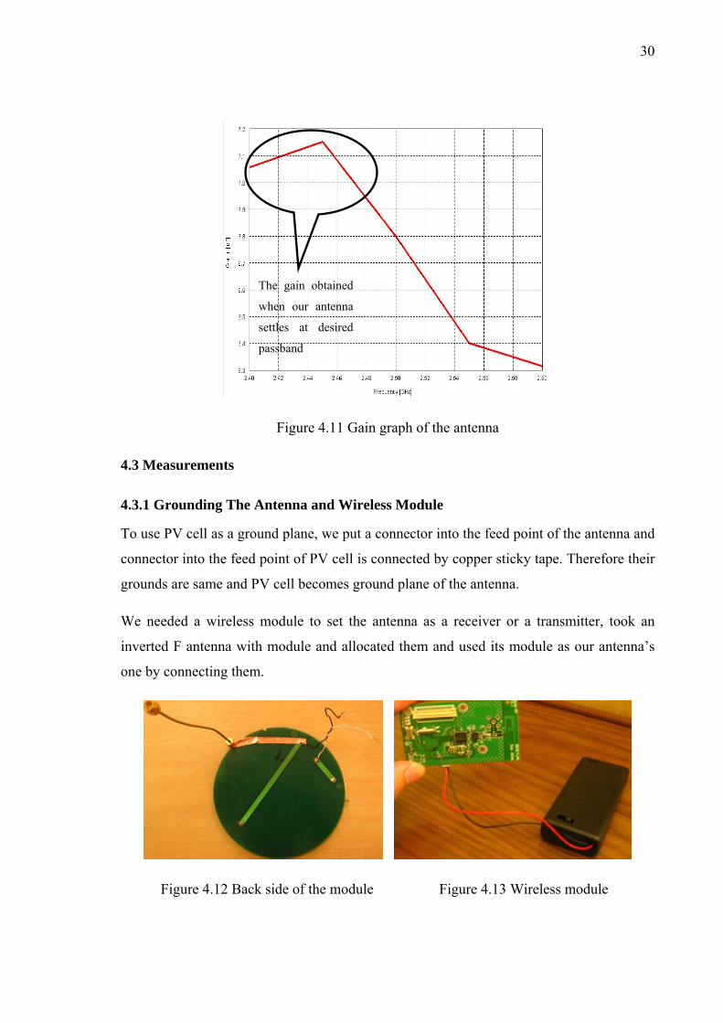
Figure 4.11 Gain graph of the antenna
4.3 Measurements
4.3.1 Grounding The Antenna and Wireless Module
To use PV cell as a ground plane, we put a connector into the feed point of the antenna and
connector into the feed point of PV cell is connected by copper sticky tape. Therefore their
grounds are same and PV cell becomes ground plane of the antenna.
We needed a wireless module to set the antenna as a receiver or a transmitter, took an
inverted F antenna with module and allocated them and used its module as our antenna’s
one by connecting them.
Figure 4.12 Back side of the module Figure 4.13 Wireless module
The gain obtained
when our antenna
settles at desired
passband

31
4.3.2 Determination of VSWR
We used the network analyzer to view how much VSWR has the antenna at
different frequencies. Before the measurement of VSWR, we made some arrangements.
We used the calibration kit to eliminate the effect of measurement cable. We can think
about calibration job as putting an offset and we put an offset. The sticky tape is special
dielectric material which does not affect the measurements, to integrate the antenna with
PV cell. The dielectric material is used for holding the antenna, it is also for good
measuring.
Figure 4.14 antenna VSWR measurement setup
After measurements with network analyzer, we have this graph. It shows that at the
passband VSWR values are enough for our design. It also says that at passband, VSWR is
samller than even 2 which is very good result for matching.

32
Figure 4.15 VSWR measured by network analyzer
This table compares the desired values with the simulated values:
Table 4.2 Comparison table between desired and simulated values
So, our simulated values are better than desired values.

33
4.3.2 Measurement of Antenna Directivity Using Spectrum Analyser
In this section, the goal is to understand our antenna works sufficiently or not by
using different kinds of receiver and transmitter antennas.
Here is the placements of the antennas:
270 degree elevation back to back side by side
Monopole antenna
Figure 4.16 Placements of the antennas
We do not have a device measuring radiation pattern, so transmitter and receiver powers
are taken to have an idea about radiation of the antenna.
Trans. Inv. F-Rec. Inv. F / bb3 Trans. Inv. F-Rec. Our antenna/ bb
Figure 4.17 VSWR Graphs of The Antenna - Section 1 3 bb:back to back

34
Trans. Inv. F4-Rec. Inv. F/ss5 Trans. Inv. F-Rec. Our antenna /ss
Trans. Inv. F-Rec. Our antenna 90°ele6 Trans. Our antenna -Rec. Mon./ 0°
Trans. Our antenna -Rec. Mon7 /90 Trans. Our antenna -Rec. Mon/90°ele
4 Inv. F: inverted F antenna
5 ss: side to side
6 ele: elevation
7 Mon: monopole antenna
Figure 4.18 VSWR Graphs of The Antenna - Section 2

35
Trans. Our antenna -Rec. Mon/270°deg Trans. Inv. F- Rec. Mon
Figure 4.19 VSWR Graphs of The Antenna - Section 3
Table 4.3 Summary of measurement of antenna directivity
Transmitter Inverted F with 18 dBm Power
Received Power Receiver Inverted F Receiver Our
antenna Receiver Monopole
face-to-face (bb) -21.68 -22.66
-36.29 side-to-side (ss) -29.49 -28.34
Transmitter Our antenna with 18 dBm Power
Received Power at
Monopole Antenna
0° 90° 90° Elevation 270° Elevation
-26.68 -46.15 -32.72 -40.69

36
5. CONCLUSIONS The solar panel is modified to function both as a solar panel and as a patch antenna.
The combined use of solar cell and patch antenna allows for dual usage of antenna ground
and solar cell, which otherwise, becomes practically challenging due to limited space.
PV cell does not lose its main characteristics when integrated with edge-fed
microstrip patch antenna. It still provides enough power for the rechargeable batteries. This
means our antenna integrated with solar module can stay operational without an external
power source, which, in turn, extends the life of the transmitter module tremendously. A
charging circuit is also designed and tested to prove that the solar module indeed charges
the battery system and can be used as a power supply module for the wireless sensor node.
The directivity and VSWR of the antenna, impedance matching are optimized
especially by changing the placement of feed line in FEKO. Using solar module as a
ground plane of the antenna is an important factor to obtain an improved gain when
compared to on-board antenna modules.
Due to unavailability of an anechoic chamber at the university and at the
neighboring institutions, we were able to make received-power measurements which are
directly related to antenna gain. Received power measurements of the designed antenna
exhibits much better performance when it is compared to inverted-F and monopole
antennas.
Figure 5.1 The microstrip patch antenna integrated PV cell with charger circuit

37
REFERENCES [1] Agent: Randall B. Bateman Bateman IP Law Group - Salt Lake City, UT, US;
Inventor: Glenn B. Dixon; USPTO Applicaton #: 20080055177 from
http://www.freshpatents.com/Combined-solar-panel-and-antenna-
dt20080306ptan20080055177.
[2] http://www.panasonic.com/industrial/battery/oem/chem/nicmet
[3] Ons, M.J.R.; Shynu, S.V.; Ammann, M.J.; McCormack, S.; Norton, B.“Investigation
on Proximity-Coupled Microstrip Integrated PV Antenna”, IEEE Antennas and
Propagation, 2007. EuCAP 2007, pp. 1 – 3.
[4] Chang, K. : Rf and Microwave Wireless Systems. John Wiley and Sons Inc., 2000.
[5] Shynu, S.V.; Ons, M.J.R.; Ammann, M.J.; McCormack, S.; Norton, B.; “A metal plate
solar antenna for UMTS pico-cell base station” IEEE Antennas and Propagation
Conference, LAPC 2008, Loughborough, 17-18 March 2008, pp. 373 – 376.
[6] Henze, N.; Giere, A.; Fruchting, H.; Hofmann, P.; “GPS patch antenna with
photovoltaic solar cells for vehicular applications”, Vehicular Technology Conference,
2003. VTC 2003 volume 1, pp:50 – 54.
[7] http://datasheet.digchip.com/291/291-02426-0-LM2574.pdf
[8] Nurulrodziah Bt Abdul Ghafar, “Design of a compact Microstrip Antenna at 2.4 GHz”,
Universiti Teknologi Malaysia, Borang Pengesahan Status Thesis, 2005.
[9] Nakar, P. S. “ Design of a Compact Microstrip Patch Antenna for Use in
Wireless/Cellular Devices,”. Florida State University, 2007.
Related Documents