BUF PGA A = 1:128 + Clock Generator Serial Interface 2nd-Order Modulator GND V DD IN+ IN– V REF+ V REF– X IN X OUT PDWN DRDY SCLK D IN D OUT CS MUX A IN 0/D0 A IN 1/D1 A IN 2/D2 A IN 3/D3 A IN 4/D4 A IN 5/D5 A IN 6/D6 A IN 7/D7 Controller Registers Digital Filter 2A µ V DD Offset DAC GND 2A µ ADS1243-HT www.ti.com SBAS525 – DECEMBER 2011 24-BIT ANALOG-TO-DIGITAL CONVERTER Check for Samples: ADS1243-HT 1FEATURES 2• 24-Bits No Missing Codes SUPPORTS EXTREME TEMPERATURE APPLICATIONS • Simultaneous 50-Hz and 60-Hz Rejection (–90 dB Minimum) • Controlled Baseline • 0.0025% INL • One Assembly/Test Site • PGA Gains From 1 to 128 • One Fabrication Site • Single-Cycle Settling • Available in Extreme (–55°C/210°C) Temperature Range (1) • Programmable Data Output Rates • Extended Product Life Cycle • External Differential Reference of 0.1 V to 5 V • Extended Product-Change Notification • On-Chip Calibration • Product Traceability • SPI™ Compatible • Texas Instruments’ high temperature products • 2.7 V to 5.25 V Supply Range utilize highly optimized silicon (die) solutions • 600-µW Power Consumption with design and process enhancements to • Up to Eight Input Channels maximize performance over extended • Up to Eight Data I/O temperatures. All devices are characterized and qualified for 1000 hours of continuous APPLICATIONS operating life at maximum rated temperatures. • Down-Hole Drilling • High Temperature Environments • Vibration/Modal Analysis • Multi-Channel Data Acquisition • Acoustics/Dynamic Strain Gauges • Pressure Sensors (1) Custom temperature ranges available DESCRIPTION The ADS1243 is a precision, wide dynamic range, delta-sigma, analog-to-digital (A/D) converter with 24-bit resolution operating from 2.7-V to 5.25-V supplies. This delta-sigma, A/D converter provides up to 24 bits of no missing code performance and effective resolution of 21 bits. The input channels are multiplexed. Internal buffering can be selected to provide a very high input impedance for direct connection to transducers or low-level voltage signals. Burnout current sources are provided that allow for the detection of an open or shorted sensor. An 8-bit digital-to-analog converter (DAC) provides an offset correction with a range of 50% of the FSR (Full-Scale Range). 1 Please be aware that an important notice concerning availability, standard warranty, and use in critical applications of Texas Instruments semiconductor products and disclaimers thereto appears at the end of this data sheet. 2All trademarks are the property of their respective owners. PRODUCTION DATA information is current as of publication date. Copyright © 2011, Texas Instruments Incorporated Products conform to specifications per the terms of the Texas Instruments standard warranty. Production processing does not necessarily include testing of all parameters.

Welcome message from author
This document is posted to help you gain knowledge. Please leave a comment to let me know what you think about it! Share it to your friends and learn new things together.
Transcript

BUF PGA
A = 1:128
+
Clock Generator
Serial Interface
2nd-Order
Modulator
GND
VDD
IN+
IN–
VREF+ VREF– XIN XOUT
PDWN DRDY
SCLK
DIN
DOUT
CS
MUX
AIN0/D0
AIN1/D1
AIN2/D2
AIN3/D3
AIN4/D4
AIN5/D5
AIN6/D6
AIN7/D7
Controller RegistersDigital
Filter
2 Aµ
VDD
Offset
DAC
GND
2 Aµ
ADS1243-HT
www.ti.com SBAS525 –DECEMBER 2011
24-BIT ANALOG-TO-DIGITAL CONVERTERCheck for Samples: ADS1243-HT
1FEATURES2• 24-Bits No Missing Codes SUPPORTS EXTREME TEMPERATURE
APPLICATIONS• Simultaneous 50-Hz and 60-Hz Rejection(–90 dB Minimum) • Controlled Baseline
• 0.0025% INL • One Assembly/Test Site• PGA Gains From 1 to 128 • One Fabrication Site• Single-Cycle Settling • Available in Extreme (–55°C/210°C)
Temperature Range (1)• Programmable Data Output Rates• Extended Product Life Cycle• External Differential Reference of 0.1 V to 5 V• Extended Product-Change Notification• On-Chip Calibration• Product Traceability• SPI™ Compatible• Texas Instruments’ high temperature products• 2.7 V to 5.25 V Supply Range
utilize highly optimized silicon (die) solutions• 600-µW Power Consumptionwith design and process enhancements to• Up to Eight Input Channelsmaximize performance over extended
• Up to Eight Data I/O temperatures. All devices are characterizedand qualified for 1000 hours of continuous
APPLICATIONS operating life at maximum rated temperatures.• Down-Hole Drilling• High Temperature Environments• Vibration/Modal Analysis• Multi-Channel Data Acquisition• Acoustics/Dynamic Strain Gauges• Pressure Sensors
(1) Custom temperature ranges available
DESCRIPTIONThe ADS1243 is a precision, wide dynamic range, delta-sigma, analog-to-digital (A/D) converter with 24-bitresolution operating from 2.7-V to 5.25-V supplies. This delta-sigma, A/D converter provides up to 24 bits of nomissing code performance and effective resolution of 21 bits.
The input channels are multiplexed. Internal buffering can be selected to provide a very high input impedance fordirect connection to transducers or low-level voltage signals. Burnout current sources are provided that allow forthe detection of an open or shorted sensor. An 8-bit digital-to-analog converter (DAC) provides an offsetcorrection with a range of 50% of the FSR (Full-Scale Range).
1
Please be aware that an important notice concerning availability, standard warranty, and use in critical applications of TexasInstruments semiconductor products and disclaimers thereto appears at the end of this data sheet.
2All trademarks are the property of their respective owners.
PRODUCTION DATA information is current as of publication date. Copyright © 2011, Texas Instruments IncorporatedProducts conform to specifications per the terms of the TexasInstruments standard warranty. Production processing does notnecessarily include testing of all parameters.
ADS1243-HT
SBAS525 –DECEMBER 2011 www.ti.com
The Programmable Gain Amplifier (PGA) provides selectable gains of 1 to 128 with an effective resolution of 19bits at a gain of 128. The A/D conversion is accomplished with a second-order delta-sigma modulator andprogrammable FIR filter that provides a simultaneous 50-Hz and 60-Hz notch. The reference input is differentialand can be used for ratiometric conversion.
The serial interface is SPI compatible. Up to eight bits of data I/O are also provided that can be used for input oroutput. The ADS1243 is designed for high-resolution measurement applications in smart transmitters, industrialprocess control, weight scales, chromatography and portable instrumentation.
ORDERING INFORMATION (1)
TA PACKAGE ORDERABLE PART NUMBER TOP-SIDE MARKING
JD ADS1243SJD ADS1243SJD–55°C to 210°C
KGD ADS1243SKGD1 NA
(1) For the most current package and ordering information, see the Package Option Addendum at the end of this document, or see the TIWeb site at www.ti.com.
ABSOLUTE MAXIMUM RATINGSover operating free-air temperature range (unless otherwise noted) (1)
VALUE UNIT
VDD to GND –0.3 to 6 V
Input Current 100, Momentary mA
Input Current 10, Continuous mA
AIN GND – 0.5 to VDD + 0.5 V
Digital Input Voltage to GND –0.3V to VDD + 0.3 V
Digital Output Voltage to GND –0.3V to VDD + 0.3 V
Maximum Junction Temperature 215 °COperating Temperature Range –55 to 210 °CStorage Temperature Range –65 to 100 °C
(1) Stresses above those listed under Absolute Maximum Ratings may cause permanent damage to the device. Exposure to absolutemaximum conditions for extended periods may affect device reliability.
THERMAL CHARACTERISTICSover operating free-air temperature range (unless otherwise noted)
PARAMETER MIN TYP MAX UNIT
θJC Junction-to-case thermal resistance HKJ package 8.1 °C/W
DIGITAL CHARACTERISTICSVDD 2.7 V to 5.25 V
TA = –55°C to 125°C TA = 210°CPARAMETER TEST CONDITIONS UNIT
MIN TYP MAX MIN TYP MAX
Digital Input/Output
Logic Family CMOS CMOS
VIH 0.8 ● VDD VDD 0.8 ● VDD VDD V
VIL(1) GND 0.2 ● VDD GND 0.2 ● VDD V
Logic LevelVOH IOH = 1 mA VDD – 0.4 VDD – 0.4 V
VOL IOL = 1 mA GND GND + 0.4 GND GND + 0.4 V
IIH VI = VDD 10 10 µAInput Leakage
IIL VI = 0 –10 –10 µA
Master Clock Rate: 1 5 1 5 MHzfOSC
(1) VIL for XIN is GND to GND + 0.05 V.
2 Submit Documentation Feedback Copyright © 2011, Texas Instruments Incorporated
Product Folder Link(s): ADS1243-HT

ADS1243-HT
www.ti.com SBAS525 –DECEMBER 2011
DIGITAL CHARACTERISTICS (continued)VDD 2.7 V to 5.25 V
TA = –55°C to 125°C TA = 210°CPARAMETER TEST CONDITIONS UNIT
MIN TYP MAX MIN TYP MAX
Master Clock Period: 1/fOSC 200 1000 200 1000 nstOSC
ELECTRICAL CHARACTERISTICS: VDD = 5 VAll specifications VDD = 5 V, fMOD = 19.2 kHz, PGA = 1, Buffer ON, fDATA = 15 Hz,VREF ≡ (REF IN+) – (REF IN–) = 2.5 V, unless otherwise specified.
TA = –55°C to 125°C TA = 210°CPARAMETER TEST CONDITIONS UNIT
MIN TYP MAX MIN TYP MAX
ANALOG INPUT (AIN0 – AIN7)
Buffer OFF GND – 0.1 VDD + 0.1 GND – 0.1 VDD + 0.1 VAnalog Input Range
Buffer ON GND + 0.05 VDD – 1.5 GND + 0.05 VDD – 1.5 V
(In+) – (In–),See Block Diagram, ±VREF/PGA ±VREF/PGA VRANGE = 0Full-Scale Input Range
±VREF/ ±VREF/RANGE = 1 V(2 ● PGA) (2 ● PGA)
Buffer OFF 5/PGA 12/PGA MΩDifferential Input Impedance
Buffer ON 5 8 GΩ
fDATA = 3.75 Hz –3 dB 1.65 Hz
Bandwidth fDATA = 7.50 Hz –3 dB 3.44 Hz
fDATA = 15 Hz –3 dB 14.6 Hz
Programmable Gain User-Selectable Gain Ranges 1 128 1 128Amplifier
Input Capacitance 9 25 pF
Input Leakage Current Modulator OFF, T = 25°C 5 6 pA
Burnout Current Sources 2 µA
OFFSET DAC
±VREF / ±VREF /RANGE = 0 V(2 ● PGA) (2 ● PGA)Offset DAC Range
±VREF / ±VREF /RANGE = 1 V(4 ● PGA) (4 ● PGA)
Offset DAC Monotonicity 8 8 Bits
Offset DAC Gain Error ±10 ±15 %
Offset DAC Gain Error Drift 1 2.2 ppm/°C
SYSTEM PERFORMANCE
Resolution No Missing Codes 24 24 Bits
Integral Nonlinearity End Point Fit ±0.0015 ±0.0018 % of FS
ppm ofOffset Error (1) 7.5 15 FS
ppm ofOffset Drift (1) 0.02 0.04 FS/°C
Gain Error (1) 0.005 0.100 %
Gain Error Drift (1) 0.5 1.118 ppm°°C
at DC 100 94 dB
Common-Mode Rejection fCM = 60 Hz, fDATA = 15 Hz 130 100 dB
fCM = 50 Hz, fDATA = 15 Hz 120 100 dB
fSIG = 50 Hz, fDATA = 15 Hz 100 95 dBNormal-Mode Rejection
fSIG = 60 Hz, fDATA = 15 Hz 100 95 dB
Output Noise See Typical Characteristics
(1) Calibration can minimize these errors.
Copyright © 2011, Texas Instruments Incorporated Submit Documentation Feedback 3
Product Folder Link(s): ADS1243-HT

ADS1243-HT
SBAS525 –DECEMBER 2011 www.ti.com
ELECTRICAL CHARACTERISTICS: VDD = 5 V (continued)All specifications VDD = 5 V, fMOD = 19.2 kHz, PGA = 1, Buffer ON, fDATA = 15 Hz,VREF ≡ (REF IN+) – (REF IN–) = 2.5 V, unless otherwise specified.
TA = –55°C to 125°C TA = 210°CPARAMETER TEST CONDITIONS UNIT
MIN TYP MAX MIN TYP MAX
at DC,Power-Supply Rejection 80 95 79 95 dBdB = –20 log(ΔVOUT /VDD) (2)
VOLTAGE REFERENCE INPUT
Reference Input Range REF IN+, REF IN– 0 VDD 0 VDD V
VREF ≡ (REF IN+) – (REF IN–), 0.1 2.5 2.6 0.1 2.5 2.6 VRANGE = 0VREF
RANGE = 1 0.1 VDD 0.1 VDD V
Common-Mode Rejection at DC 120 98 dB
Common-Mode Rejection fVREFCM = 60 Hz, fDATA = 15 Hz 120 95 dB
Bias Current (3) VREF = 2.5 V 1.3 10 µA
POWER-SUPPLY REQUIREMENTS
Power-Supply Voltage VDD 4.75 5.25 4.75 5.25 V
PGA = 1, Buffer OFF 240 375 250 480 µA
PGA = 128, Buffer OFF 450 800 630 940 µA
PGA = 1, Buffer ON 290 425 350 585 µA
Current PGA = 128, Buffer ON 960 1400 1200 2050 µA
SLEEP Mode 60 80 µA
Read Data Continuous Mode 230 350 µA
PDWN 0.5 10 nA
Power Dissipation PGA = 1, Buffer OFF 1.2 1.9 1.3 2.52 mW
(2) ΔVOUT is a change in digital result.(3) 12-pF switched capacitor at fSAMP clock frequency.
ELECTRICAL CHARACTERISTICS: VDD = 3 VAll specifications VDD = 3 V, fMOD = 19.2 kHz, PGA = 1, Buffer ON, fDATA = 15 Hz,VREF ≡ (REF IN+) – (REF IN–) = 1.25 V, unless otherwise specified.
TA = –55°C to 125°C TA = 210°CPARAMETER TEST CONDITIONS UNIT
MIN TYP MAX MIN TYP MAX
ANALOG INPUT (AIN0 – AIN7)
Buffer OFF GND – 0.1 VDD + 0.1 GND – 0.1 VDD + 0.1 VAnalog Input Range GND +Buffer ON VDD – 1.5 GND + 0.05 VDD – 1.5 V0.05
(In+) – (In–), See Block ±VREF/ ±VREF/ VDiagram, RANGE = 0 PGA PGAFull-Scale Input VoltageRange ±VREF/ ±VREF/RANGE = 1 V(2 • PGA) (2 • PGA)
Buffer OFF 5/PGA 10/PGA MΩInput Impedance
Buffer ON 5 8 GΩ
fDATA = 3.75 Hz –3 dB 1.65 Hz
Bandwidth fDATA = 7.50 Hz –3 dB 3.44 Hz
fDATA = 15 Hz –3 dB 14.6 Hz
Programmable Gain User-Selectable Gain Ranges 1 128 1 128Amplifier
Input Capacitance 9 25 pF
Input Leakage Current Modulator OFF, T = 25°C 5 6 pA
Burnout Current Sources 2 µA
OFFSET DAC
±VREF/ ±VREF/RANGE = 0 V(2 ● PGA) (2 ● PGA)Offset DAC Range
±VREF/ ±VREF/RANGE = 1 V(4 ● PGA) (4 ● PGA)
4 Submit Documentation Feedback Copyright © 2011, Texas Instruments Incorporated
Product Folder Link(s): ADS1243-HT

ADS1243-HT
www.ti.com SBAS525 –DECEMBER 2011
ELECTRICAL CHARACTERISTICS: VDD = 3 V (continued)All specifications VDD = 3 V, fMOD = 19.2 kHz, PGA = 1, Buffer ON, fDATA = 15 Hz,VREF ≡ (REF IN+) – (REF IN–) = 1.25 V, unless otherwise specified.
TA = –55°C to 125°C TA = 210°CPARAMETER TEST CONDITIONS UNIT
MIN TYP MAX MIN TYP MAX
Offset DAC Monotonicity 8 8 Bits
Offset DAC Gain Error ±10 ±12 %
Offset DAC Gain Error Drift 1 2 ppm/°C
SYSTEM PERFORMANCE
Resolution No Missing Codes 24 24 Bits
Integral Nonlinearity End Point Fit ±0.0015 ±0.0025 % of FS
ppm ofOffset Error (1) 75 40 FS
ppm ofOffset Drift (1) 0.02 0.20 FS/°C
Gain Error (1) 0.005 0.1 %
Gain Error Drift (1) 0.5 1.118 ppm/°C
at DC 100 87 dB
Common-Mode Rejection fCM = 60 Hz, fDATA = 15 Hz 130 98 dB
fCM = 50 Hz, fDATA = 15 Hz 120 95 dB
fSIG = 50 Hz, fDATA = 15 Hz 100 90 dBNormal-Mode Rejection
fSIG = 60 Hz, fDATA = 15 Hz 100 90 dB
Output Noise See Typical Characteristics
at DC,Power-Supply Rejection 80 95 75 90 dBdB = –20 log(ΔVOUT /VDD) (2)
VOLTAGE REFERENCE INPUT
Reference Input Range REF IN+, REF IN– 0 VDD 0 VDD V
VREF ≡ (REF IN+) – 0.1 1.25 1.30 0.1 1.25 1.30 V(REF IN–), RANGE = 0VREF
RANGE = 1 0.1 VDD 0.1 2.6 V
Common-Mode Rejection at DC 120 95 dB
fVREFCM = 60 Hz,Common-Mode Rejection 120 93 dBfDATA = 15 Hz
Bias Current (3) VREF = 1.25 V 1.3 8 µA
POWER-SUPPLY REQUIREMENTS
Power-Supply Voltage VDD 2.7 3.3 2.7 3.3 V
PGA = 1, Buffer OFF 190 375 200 480 µA
PGA = 128, Buffer OFF 460 700 600 940 µA
PGA = 1, Buffer ON 240 375 350 585 µA
Current PGA = 128, Buffer ON 870 1325 1200 1800 µA
SLEEP Mode 75 110 µA
Read Data Continuous Mode 113 250 µA
PDWN = 0 0.5 7.5 nA
Power Dissipation PGA = 1, Buffer OFF 0.6 1.2 0.66 1.58 mW
(1) Calibration can minimize these errors.(2) ΔVOUT is a change in digital result.(3) 12-pF switched capacitor at fSAMP clock frequency.
Copyright © 2011, Texas Instruments Incorporated Submit Documentation Feedback 5
Product Folder Link(s): ADS1243-HT
1000
10,000
100,000
1,000,000
10,000,000
80 100 120 140 160 180 200 220
Esti
mate
d L
ife (
Ho
urs
)
Continuous T (°C)J
ADS1243-HT
SBAS525 –DECEMBER 2011 www.ti.com
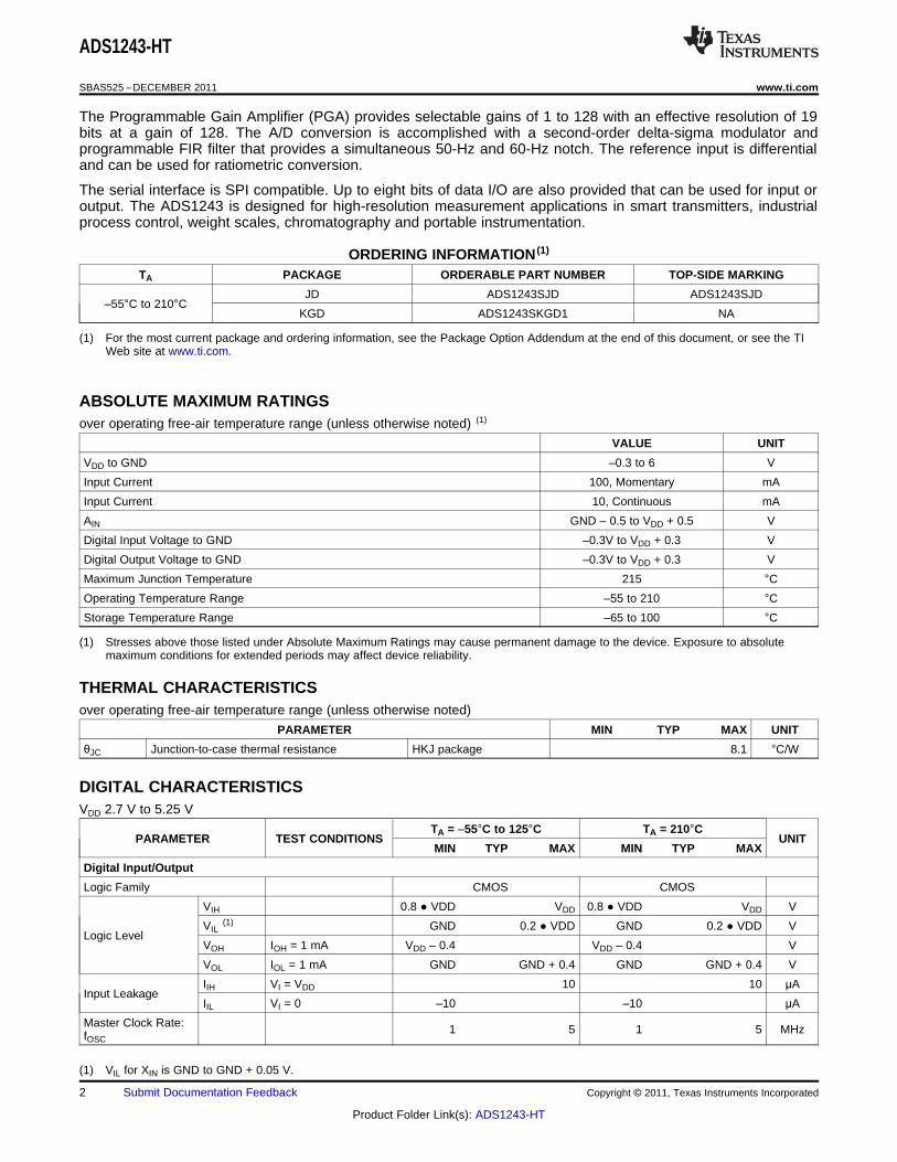
(1) See data sheet for absolute maximum and minimum recommended operating conditions.
(2) Silicon operating life design goal is 10 years at 105°C junction temperature (does not include package interconnectlife).
(3) The predicted operating lifetime vs. junction temperature is based on reliability modeling using electromigration as thedominant failure mechanism affecting device wearout for the specific device process and design characteristics.
Figure 1. ADS1243-HT Operating Life Derating Chart
6 Submit Documentation Feedback Copyright © 2011, Texas Instruments Incorporated
Product Folder Link(s): ADS1243-HT

1
2
3
4
5
6
7
8
9
10
20
19
18
17
16
15
14
13
12
11
VDD
XIN
XOUT
PDWN
VREF+
VREF–
AIN
0/D0
AIN
1/D1
AIN
4/D4
AIN
5/D5
DRDY
SCLK
DOUT
DIN
CS
GND
AIN
3/D3
AIN
2/D2
AIN
7/D7
AIN
6/D6
ADS1243-HT
www.ti.com SBAS525 –DECEMBER 2011
PIN CONFIGURATION
CDIP PACKAGE(TOP VIEW)
PIN ASSIGNMENTSPIN # NAME DESCRIPTION
1 VDD Power Supply
2 XIN Clock Input
3 XOUT Clock Output, used with crystal or ceramic resonator.
4 PDWN Active LOW. Power Down. The power down function shuts down the analog and digital circuits.
5 VREF+ Positive Differential Reference Input
6 VREF– Negative Differential Reference Input
7 AIN0/D0 Analog Input 0/Data I/O 0
8 AIN1/D1 Analog Input 1/Data I/O 1
9 AIN4/D4 Analog Input 4/Data I/O 4
10 AIN5/D5 Analog Input 5/Data I/O 5
11 AIN6/D6 Analog Input 6/Data I/O 6
12 AIN7/D7 Analog Input 7/Data I/O 7
13 AIN2/D2 Analog Input 2/Data I/O 2
14 AIN3/D3 Analog Input 3/Data I/O 3
15 GND Ground
16 CS Active LOW, Chip Select
17 DIN Serial Data Input, Schmitt Trigger
18 DOUT Serial Data Output
19 SCLK Serial Clock, Schmitt Trigger
20 DRDY Active LOW, Data Ready
Copyright © 2011, Texas Instruments Incorporated Submit Documentation Feedback 7
Product Folder Link(s): ADS1243-HT

ADS1243-HT
SBAS525 –DECEMBER 2011 www.ti.com
BARE DIE INFORMATION
BACKSIDE BOND PADDIE THICKNESS BACKSIDE FINISH POTENTIAL METALLIZATION COMPOSITION
15 mils Silicon with backgrind GND AlCu
Table 1. Bond Pad Coordinates in Microns (1)
DISCRIPTION PAD NUMBER X MIN Y MIN X MAX Y MAX
VDD 1 1268.55 2471.55 1478.15 2572.55
Connect to substrate 2 1030.45 2471.55 1132.45 2572.55
Connect to substrate 3 692.45 2471.55 902.05 2572.55
XIN 4 450.05 2471.55 552.05 2572.55
XOUT 5 6.45 2016.65 107.45 2118.65
NC 6 6.45 1721.75 107.45 1823.75
NC 7 6.45 1468.60 107.45 1570.60
PDWN 8 6.45 1224.80 107.45 1326.80
NC 9 6.45 929.95 107.45 1031.95
VREF+ 10 6.45 655.20 107.45 757.20
VREF- 11 6.45 373.25 107.45 475.25
AIN0/D0 12 361.15 3.55 462.15 105.55
AIN1/D1 13 636.45 3.55 737.45 105.55
AIN4/D4 14 911.70 3.55 1012.70 105.55
AIN5/D5 15 1186.85 3.55 1287.85 105.55
AIN6/D6 16 1466.25 3.55 1567.25 105.55
AIN7/D7 17 1742.50 3.55 1843.50 105.55
AIN2/D2 18 2017.60 3.55 2118.60 105.55
AIN3/D3 19 2292.75 3.55 2393.75 105.55
NC 20 2608.70 310.50 2709.70 412.50
GND 21 2608.75 553.25 2709.75 762.85
GND 22 2608.70 832.20 2709.70 934.20
NC 23 2608.75 1001.60 2709.75 1211.20
NC 24 2608.70 1335.65 2709.70 1437.65
CS 25 2608.70 1571.45 2709.70 1673.45
DIN 26 2608.70 1797.90 2709.70 1899.90
DOUT 27 2608.70 2076.55 2709.70 2178.55
SCLK 28 2234.80 2471.55 2336.80 2572.55
DRDY 29 1931.10 2471.55 2033.10 2572.55
NC 30 1637.90 2471.55 1739.90 2572.55
(1) For signal descriptions see the Pin Assignments table.
8 Submit Documentation Feedback Copyright © 2011, Texas Instruments Incorporated
Product Folder Link(s): ADS1243-HT

PA
D #
1
2713.55 µm
2578.9
0 µ
m
50 µm
50 µm
VDDConnect toSubstrate
Connect toSubstrate
XIN
XOUT
NC
NC
PDWN
NC
VREF+
VREF-
A 0/D0IN A 1/D1IN A 4/D4IN A 5/D5IN A 6/D6IN A 7/D7IN A 2/D2IN A 3/D3IN
NC
GND
GND
NC
NC
CS
DIN
DOUT
SCLKDRDYNC
0
0
EDGE OFSCRIBE
ADS1243-HT
www.ti.com SBAS525 –DECEMBER 2011
Copyright © 2011, Texas Instruments Incorporated Submit Documentation Feedback 9
Product Folder Link(s): ADS1243-HT

t4
MSB
(Command or Command and Data)
LSB
t5
t1t3
CS
SCLK
DIN
DOUT
NOTE: (1) Bit order = 0.
SCLK Reset Waveform
t7
MSB(1) LSB(1)
t8
t10t2
t2 t11t6
t9
t12 t14 t15
t13 t13
SCLK
Resets On
Falling Edge 300 • tOSC < t12 < 500 • tOSC
t13 : > 5 • tOSC
550 • tOSC < t14 < 750 • tOSC
1050 • tOSC < t15 < 1250 • tOSC
t17
t18
DRDY
SCLK
tDATA
t16
PDWN
t19
ADS1243-HT
SBAS525 –DECEMBER 2011 www.ti.com
TIMING DIAGRAMS
10 Submit Documentation Feedback Copyright © 2011, Texas Instruments Incorporated
Product Folder Link(s): ADS1243-HT

ADS1243-HT
www.ti.com SBAS525 –DECEMBER 2011
TIMING REQUIREMENTSPARAMETER TEST CONDITIONS MIN MAX UNIT
tOSC4 Periodst1 SCLK Period
DRDY3 Periods
t2 SCLK Pulse Width, HIGH and LOW 200 ns
t3 CS low to first SCLK Edge; Setup Time (1) 0 ns
t4 DIN Valid to SCLK Edge; Setup Time 50 ns
t5 Valid DIN to SCLK Edge; Hold Time 50 ns
Delay between last SCLK edge for DIN and first SCLK tOSCt6 50edge for DOUT: RDATA, RDATAC, RREG, WREG Periods
t7(2) SCLK Edge to Valid New DOUT 50 ns
t8(2) SCLK Edge to DOUT, Hold Time 0 ns
Last SCLK Edge to DOUT Tri-State tOSCt9 NOTE: DOUT goes tri-state immediately when CS goes 6 10 PeriodsHIGH.
tOSCRead from the device 0 Periodst10 CS LOW time after final SCLK edge.
tOSCWrite to the device 8 Periods
RREG, WREG, DSYNC, tOSCSLEEP, RDATA, 4 PeriodsRDATAC, STOPC
SELFGCAL, DRDYSELFOCAL, SYSOCAL, 2Final SCLK edge of one command until first edge SCLK Periodst11 SYSGCALof next command:DRDYSELFCAL 4 Periods
RESET (also SCLK tOSC16Reset) Periods
tOSCt16 Pulse Width 4 Periods
tOSCt17 Allowed analog input change for next valid conversion. 5000 Periods
tOSCt18 DOR update, DOR data not valid. 4 Periods
tOSCRDATAC Mode 10 Periodst19 First SCLK after DRDY goes LOW:
tOSCAny other mode 0 Periods
(1) CS may be tied LOW.(2) Load = 20 pF|| 10 kΩ to GND.
Copyright © 2011, Texas Instruments Incorporated Submit Documentation Feedback 11
Product Folder Link(s): ADS1243-HT

22
21
20
19
18
17
16
15
PGA Setting
EN
OB
(rm
s)
1 2 4 8 16 1286432
DR = 10
DR = 00
DR = 01
Buffer ON
21.5
21.0
20.5
20.0
19.5
19.0
18.5
18.0
17.5
17.0
PGA Setting
1 2 4 8 16 1286432
EN
OB
(rm
s)
Buffer OFF
DR = 10
DR = 01
DR = 00
2.0
1.8
1.6
1.4
1.2
1.0
0.8
0.6
0.4
0.2
0
VIN (V)
–2.5 –1.5 0.5–0.5 1.5 2.5
Nois
e (
rms, ppm
of F
S)
20.5
20.0
19.5
19.0
18.5
18.0
17.5
17.0
16.5
16.0
PGA Setting
1 2 4 8 16 64 12832
EN
OB
(rm
s)
Buffer OFF, V REF = 1.25V
DR = 10
DR = 00
DR = 01
Frequency of Power Supply (Hz)
1 10 1k100 10k 100k
PS
RR
(d
B)
140
120
100
80
60
40
20
0
Buffer ON
140
120
100
80
60
40
20
0
Frequency of Power Supply (Hz)
1 10 100 1k 10k 100k
CM
RR
(dB
)
Buffer ON
ADS1243-HT
SBAS525 –DECEMBER 2011 www.ti.com
TYPICAL CHARACTERISTICSAll specifications VDD = 5 V, fOSC = 2.4576 MHz, PGA = 1, fDATA = 15 Hz, and VREF ≡ (REF IN+) – (REF IN–) = 2.5 V,
unless otherwise specified.
EFFECTIVE NUMBER OF BITS EFFECTIVE NUMBER OF BITSvs vs
PGA SETTING PGA SETTING
EFFECTIVE NUMBER OF BITS NOISEvs vs
PGA SETTING INPUT SIGNAL
COMMON-MODE REJECTION RATIO POWER SUPPLY REJECTION RATIOvs vs
FREQUENCY FREQUENCY
12 Submit Documentation Feedback Copyright © 2011, Texas Instruments Incorporated
Product Folder Link(s): ADS1243-HT

50
0
–50
–100
–150
–250
–200
Offset (p
pm
of F
S)
Temperature (°C)
–55 –35 –15 5 25 45 65 85 105 125 145 165 185 205
PGA16
PGA64
PGA128
PGA1
Ga
in (
No
rma
lize
d)
0.980
0.984
0.988
0.992
0.996
1.000
1.004
1.008
1.012
1.016
1.020
Temperature (°C)
–55 –35 –15 5 25 45 65 85 105 125 145 165 185 205
10
8
6
4
2
0
–2
–4
–6
–8
–10
VIN (V)
–2.5 –2.0 –1.0 – 0.5–1.5 00 .5 1. 0 1.5 2.0 2.5
INL
(ppm
of F
S)
–40°C
+25°C
+85°C
Curr
ent (µ
A)
325
300
275
250
225
175
200
Temperature (°C)
–55 –35 –15 5 25 45 65 85 105 125 145 165 185 205
350
300
250
200
150
100
50
0
–50
VDD (V)
3.0 3 .253 .5 3.75 4.0 4. 254 .5 4.75 5.0
Cu
rre
nt
(µA
)
Normal4.91MHz
Normal2.45MHz
SLEEP4.91MHz
SLEEP2.45MHz
Power Down
300
250
200
150
100
50
0
VDD (V)
3.0 3.5 4.04 .5 5.0
I DIG
ITA
L(µ
A)
Normal4.91MHz
Normal2.45MHz
SLEEP2.45MHzPower Down
SLEEP4.91MHz
ADS1243-HT
www.ti.com SBAS525 –DECEMBER 2011
TYPICAL CHARACTERISTICS (continued)All specifications VDD = 5 V, fOSC = 2.4576 MHz, PGA = 1, fDATA = 15 Hz, and VREF ≡ (REF IN+) – (REF IN–) = 2.5 V,
unless otherwise specified.OFFSET GAIN
vs vsTEMPERATURE TEMPERATURE
(Cal AT 25°C) (Cal AT 25°C)
INTEGRAL NONLINEARITY CURRENTvs vs
INPUT SIGNAL TEMPERATURE
CURRENT SUPPLY CURRENTvs vs
VOLTAGE SUPPLY
Copyright © 2011, Texas Instruments Incorporated Submit Documentation Feedback 13
Product Folder Link(s): ADS1243-HT

Offse
t (p
pm
of
FS
R)
–250
–200
–150
–100
–50
0
50
100
150
200
Temperature (°C)
–55 –35 –15 5 25 45 65 85 105 125 145 165 185 205
3500
3000
2500
2000
1500
1000
500
0
10k ReadingsVIN = 0V
ppm of FS
–3.5 –3.0
Nu
mb
er
of
Occu
rre
nce
s
–2.5 –2.0 –1.5 –1 –0.5 0 0.5 1.0 1.5 2.0 2.5 3.0 3.5
0.9995
0.9996
0.9997
0.9998
0.9999
1.0001
1.0002
1.0003
1.0004
1.0005
Ga
in (
No
rma
lize
d)
1.0000
Temperature (°C)
–55 –35 –15 5 25 45 65 85 105 125 145 165 185 205
0.8
0.7
0.6
0.5
0.4
0.3
0.2
0.1
0
Offset DAC Setting
No
ise
(rm
s, pp
m o
f F
S)
–128 –96 –64 –32 0 32 64 96 128
ADS1243-HT
SBAS525 –DECEMBER 2011 www.ti.com
TYPICAL CHARACTERISTICS (continued)All specifications VDD = 5 V, fOSC = 2.4576 MHz, PGA = 1, fDATA = 15 Hz, and VREF ≡ (REF IN+) – (REF IN–) = 2.5 V,
unless otherwise specified.OFFSET DAC OFFSET
vsTEMPERATURE
NOISE HISTOGRAM (Cal AT 25°C)
OFFSET DAC GAINvs OFFSET DAC NOISE
TEMPEARTURE vs(Cal AT 25°C) SETTING
14 Submit Documentation Feedback Copyright © 2011, Texas Instruments Incorporated
Product Folder Link(s): ADS1243-HT

AIN3/D3
AIN4/D4
AIN5/D5
AIN6/D6
AIN0/D0
AIN1/D1
AIN2/D2
AIN7/D7
Burnout Current Source
Burnout Current Source
GND
VDD
Input
Buffer
ADS1243-HT
www.ti.com SBAS525 –DECEMBER 2011
OVERVIEW
INPUT MULTIPLEXER
The input multiplexer provides for any combination of differential inputs to be selected on any of the inputchannels, as shown in Figure 2. For example, if AIN0 is selected as the positive differential input channel, anyother channel can be selected as the negative terminal for the differential input channel. With this method, it ispossible to have up to seven single-ended input channels or four independent differential input channels for theADS1243.
The ADS1243 features a single-cycle settling digital filter that provides valid data on the first conversion after anew channel selection. In order to minimize the settling error, synchronize MUX changes to the conversionbeginning, which is indicated by the falling edge of DRDY. In other words, issuing a MUX change through theWREG command immediately after DRDY goes LOW minimizes the settling error. Increasing the time betweenthe conversion beginning (DRDY goes LOW) and the MUX change command (tDELAY) results in a settling error inthe conversion data, as shown in Figure 3.
Figure 2. Input Multiplexer Configuration
Copyright © 2011, Texas Instruments Incorporated Submit Documentation Feedback 15
Product Folder Link(s): ADS1243-HT

SETTLING ERROR vs DELAY TIME
fCLK = 2.4576MHz
Delay Time, tDELAY (ms)
Se
ttlin
g E
rro
r (%
)
2 4 6 8 10 12 14 160
10
1
0.1
0.01
0.001
0.0001
0.00001
0.000001
New Conversion Begins,
Complete Previous Conversion New Conversion Complete
tDELAY
MSB LSB
DRDY
DIN
SCLK
Previous Conversion Data
OPEN CIRCUIT
VDD
VDD
0V
2 Am
2 Am
CODE = 0x7FFFFFH
ADC
ADS1243-HT
SBAS525 –DECEMBER 2011 www.ti.com
Figure 3. Input Multiplexer Configuration
BURNOUT CURRENT SOURCES
The Burnout Current Sources can be used to detect sensor short-circuit or open-circuit conditions. Setting theBurnout Current Sources (BOCS) bit in the SETUP register activates two 2µA current sources called burnoutcurrent sources. One of the current sources is connected to the converter’s negative input and the other isconnected to the converter’s positive input.
Figure 4 shows the situation for an open-circuit sensor. This is a potential failure mode for many kinds ofremotely connected sensors. The current source on the positive input acts as a pull-up, causing the positive inputto go to the positive analog supply, and the current source on the negative input acts as a pull-down, causing thenegative input to go to ground. The ADS1243 therefore outputs full-scale (7FFFFF Hex).
Figure 5 shows a short-circuited sensor. Since the inputs are shorted and at the same potential, the ADS1243signal outputs are approximately zero. (Note that the code for shorted inputs is not exactly zero due to internalseries resistance, low-level noise and other error sources.)
Figure 4. Burnout Detection While Sensor is Open-Circuited.
16 Submit Documentation Feedback Copyright © 2011, Texas Instruments Incorporated
Product Folder Link(s): ADS1243-HT

SHORT
CIRCUIT
VDD
VDD
/2
VDD
/2
2 Am
2 Am
CODE ≅0ADC
ADS1243-HT
www.ti.com SBAS525 –DECEMBER 2011
Figure 5. Burnout Detection While Sensor is Short-Circuited.
INPUT BUFFER
The input impedance of ADS1243 without the buffer enabled is approximately 5MΩ/PGA. For systems requiringvery high input impedance, the ADS1243 provides a chopper-stabilized differential FET-input voltage buffer.When activated, the buffer raises the ADS1243 input impedance to approximately 5 GΩ.
The buffer’s input range is approximately 50mV to VDD – 1.5 V. The buffer’s linearity will degrade beyond thisrange. Differential signals should be adjusted so that both signals are within the buffer’s input range.
The buffer can be enabled using the BUFEN pin or the BUFEN bit in the ACR register. The buffer is on when theBUFEN pin is high and the BUFEN bit is set to one. If the BUFEN pin is low, the buffer is disabled. If the BUFENbit is set to zero, the buffer is also disabled.
The buffer draws additional current when activated. The current required by the buffer depends on the PGAsetting. When the PGA is set to 1, the buffer uses approximately 50 µA; when the PGA is set to 128, the bufferuses approximately 500µA.
PGA
The Programmable Gain Amplifier (PGA) can be set to gains of 1, 2, 4, 8, 16, 32, 64, or 128. Using the PGA canimprove the effective resolution of the A/D converter. For instance, with a PGA of 1 on a 5-V full-scale signal, theA/D converter can resolve down to 1 µV. With a PGA of 128 and a full-scale signal of 39 mV, the A/D convertercan resolve down to 75 nV. VDD current increases with PGA settings higher than 4.
OFFSET DAC
The input to the PGA can be shifted by half the full-scale input range of the PGA using the Offset DAC (ODAC)register. The ODAC register is an 8-bit value; the MSB is the sign and the seven LSBs provide the magnitude ofthe offset. Using the offset DAC does not reduce the performance of the A/D converter. For more details on theODAC in the ADS1243, please refer to TI application report SBAA077 (available through the TI website).
MODULATOR
The modulator is a single-loop second-order system. The modulator runs at a clock speed (fMOD) that is derivedfrom the external clock (fOSC). The frequency division is determined by the SPEED bit in the SETUP register, asshown in Table 2.
Copyright © 2011, Texas Instruments Incorporated Submit Documentation Feedback 17
Product Folder Link(s): ADS1243-HT

ADS1243-HT
SBAS525 –DECEMBER 2011 www.ti.com
Table 2. Output Configuration
DR BITSSPEED 1st NOTCHfOSC fMODBIT FREQUENCY00 01 10
0 19,200 Hz 15 Hz 7.5 Hz 3.75 Hz 50/60 Hz2.4576 MHz
1 9,600 Hz 7.5 Hz 3.75 Hz 1.875 Hz 25/30 Hz
0 38,400 Hz 30 Hz 15 Hz 7.5 Hz 100/120 Hz4.9152 MHz
1 19,200 Hz 15 Hz 7.5 Hz 3.75 Hz 50/60 Hz
CALIBRATION
The offset and gain errors can be minimized with calibration. The ADS1243 supports both self and systemcalibration.
Self-calibration of the ADS1243 corrects internal offset and gain errors and is handled by three commands:SELFCAL, SELFGAL, and SELFOCAL. The SELFCAL command performs both an offset and gain calibration.SELFGCAL performs a gain calibration and SELFOCAL performs an offset calibration, each of which takes twotDATA periods to complete. During self-calibration, the ADC inputs are disconnected internally from the input pins.The PGA must be set to 1 prior to issuing a SELFCAL or SELFGCAL command. Any PGA is allowed whenissuing a SELFOCAL command. For example, if using PGA = 64, first set PGA = 1 and issue SELFGCAL.Afterwards, set PGA = 64 and issue SELFOCAL. For operation with a reference voltage greater than (VDD – 1.5)volts, the buffer must also be turned off during gain self-calibration to avoid exceeding the buffer input range.
System calibration corrects both internal and external offset and gain errors. While performing system calibration,the appropriate signal must be applied to the inputs. The system offset calibration command (SYSOCAL)requires a zero input differential signal (see Table 5). It then computes the offset that nullifies the offset in thesystem. The system gain calibration command (SYSGCAL) requires a positive full-scale input signal. It thencomputes a value to nullify the gain error in the system. Each of these calibrations takes two tDATA periods tocomplete. System gain calibration is recommended for the best gain calibration at higher PGAs.
Calibration should be performed after power on, a change in temperature, or a change of the PGA. The RANGEbit (ACR bit 2) must be zero during calibration.
Calibration removes the effects of the ODAC; therefore, disable the ODAC during calibration, and enable againafter calibration is complete.
At the completion of calibration, the DRDY signal goes low, indicating the calibration is finished. The first dataafter calibration should be discarded since it may be corrupt from calibration data remaining in the filter. Thesecond data is always valid.
EXTERNAL VOLTAGE REFERENCE
The ADS1243 requires an external voltage reference. The selection for the voltage reference value is madethrough the ACR register.
The external voltage reference is differential and is represented by the voltage difference between the pins:+VREF and –VREF. The absolute voltage on either pin, +VREF or –VREF, can range from GND to VDD. However, thefollowing limitations apply:• For VDD = 5 V and RANGE = 0 in the ACR, the differential VREF must not exceed 2.5 V.• For VDD = 5 V and RANGE = 1 in the ACR, the differential VREF must not exceed 5 V.• For VDD = 3 V and RANGE = 0 in the ACR, the differential VREF must not exceed 1.25 V.• For VDD = 3 V and RANGE = 1 in the ACR, the differential VREF must not exceed 2.5 V.
CLOCK GENERATOR
The clock source for ADS1243 can be provided from a crystal, oscillator, or external clock. When the clocksource is a crystal, external capacitors must be provided to ensure start-up and stable clock frequency. This isshown in both Figure 6 and Table 3. XOUT is only for use with external crystals and it should not be used as aclock driver for external circuitry.
18 Submit Documentation Feedback Copyright © 2011, Texas Instruments Incorporated
Product Folder Link(s): ADS1243-HT

C1
Crystal
XIN
XOUTC2
ADS1243-HT
www.ti.com SBAS525 –DECEMBER 2011
Figure 6. Crystal Connection.
Table 3. Recommended Crystals
CLOCK PARTFREQUENCY C1 C2SOURCE NUMBER
Crystal 2.4576 0-20 pF 0-20 pF ECS, ECSD 2.45 – 32
Crystal 4.9152 0-20 pF 0-20 pF ECS, ECSL 4.91
Crystal 4.9152 0-20 pF 0-20 pF ECS, ECSD 4.91
Crystal 4.9152 0-20 pF 0-20 pF CTS, MP 042 4M9182
DIGITAL FILTER
The ADS1243 has a 1279 tap linear phase Finite Impulse Response (FIR) digital filter that a user can configurefor various output data rates. When a 2.4576-MHz crystal is used, the device can be programmed for an outputdata rate of 15 Hz, 7.5 Hz, or 3.75 Hz. Under these conditions, the digital filter rejects both 50Hz and 60Hzinterference. Figure 7 shows the digital filter frequency response for data output rates of 15 Hz, 7.5 Hz, and 3.75Hz.
If a different data output rate is desired, a different crystal frequency can be used. However, the rejectionfrequencies shift accordingly. For example, a 3.6864-MHz master clock with the default register condition has:
(3.6864 MHz/2.4576 MHz) ● 15 Hz = 22.5 Hz data output rate
and the first and second notch is:1.5 ● (50 Hz and 60 Hz) = 75 Hz and 90 Hz
Copyright © 2011, Texas Instruments Incorporated Submit Documentation Feedback 19
Product Folder Link(s): ADS1243-HT

DATA –3dB
OUTPUT RATE BANDWIDTH f IN = 50 ± 0.3Hz fIN = 60 ± 0.3Hz fIN = 50 ± 1Hz fIN = 60 ± 1Hz
15Hz 14.6Hz –80.8dB –87.3dB –68.5dB –76.1dB
7.5Hz 3.44Hz –85.9dB –87.4dB –71.5dB –76.2dB
3.75Hz 1.65Hz –93.8dB –88.6dB –86.8dB –77.3dB
FREQUENCY RESPONSE FROM 45Hz to 65Hz
WHEN fDATA = 15Hz
Frequency (Hz)
–40
–50
–60
–70
–80
–90
–100
–110
–120
–130
–140
Ma
gn
itu
de
(d
B)
FREQUENCY RESPONSE FROM 45Hz to 65Hz
WHEN fDATA = 7.5Hz
Frequency (Hz)
–40
–50
–60
–70
–80
–90
–100
–110
–120
–130
–140
Ma
gn
itu
de
(d
B)
FREQUENCY RESPONSE FROM 45Hz to 65Hz
WHEN fDATA = 3.75Hz
Frequency (Hz)
–40
–50
–60
–70
–80
–90
–100
–110
–120
–130
–140
Ma
gn
itu
de
(d
B)
ADS1243
FILTER RESPONSE WHEN fDATA = 15Hz
Frequency (Hz)
0
–20
–40
–60
–80
–100
–120
–140
–160
–180
0 20
Ga
in (
dB
)
ADS1243
FILTER RESPONSE WHEN fDATA = 7.5Hz
Frequency (Hz)
0
–20
–40
–60
–80
–100
–120
–140
–160
–180
Ga
in (
dB
)
ADS1243
FILTER RESPONSE WHEN fDATA = 3.75Hz
Frequency (Hz)
fOSC = 2.4576MHz, SPEED = 0 or fOSC = 4.9152MHz, SPEED = 1
0
–20
–40
–60
–80
–100
–120
–140
–160
–180
Ga
in (
dB
)
ATTENUATION
40 60 80 100 120 140 160 180 200
0 20 40 60 80 100 120 140 160 180 200
0 20 40 60 80 100 120 140 160 180 200
55 60 6545 50
55 60 6545 50
55 60 6545 50
ADS1243-HT
SBAS525 –DECEMBER 2011 www.ti.com
Figure 7. Filter Frequency Responses
20 Submit Documentation Feedback Copyright © 2011, Texas Instruments Incorporated
Product Folder Link(s): ADS1243-HT

IOCON
AINx/Dx
To Analog Mux
DIO WRITE
DIR
DIO READ
ADS1243-HT
www.ti.com SBAS525 –DECEMBER 2011
DATA I/O INTERFACE
The ADS1243 has eight pins that serve a dual purpose as both analog inputs and data I/O. These pins areconfigured through the IOCON, DIR, and DIO registers and can be individually configured as either analog inputsor data I/O. See Figure 8 for the equivalent schematic of an Analog/Data I/O pin.
The IOCON register defines the pin as either an analog input or data I/O. The power-up state is an analog input.If the pin is configured as an analog input in the IOCON register, the DIR and DIO registers have no effect on thestate of the pin.
If the pin is configured as data I/O in the IOCON register, then DIR and DIO are used to control the state of thepin. The DIR register controls the direction of the data pin, either as an input or output. If the pin is configured asan input in the DIR register, then the corresponding DIO register bit reflects the state of the pin. Make sure thepin is driven to a logic one or zero when configured as an input to prevent excess current dissipation. If the pin isconfigured as an output in the DIR register, then the corresponding DIO register bit value determines the state ofthe output pin (0 = GND, 1 = VDD).
It is still possible to perform A/D conversions on a pin configured as data I/O. This may be useful as a test mode,where the data I/O pin is driven and an A/D conversion is done on the pin.
Figure 8. Analog/Data Interface Pin
SERIAL PERIPHERAL INTERFACE
The Serial Peripheral Interface (SPI) allows a controller to communicate synchronously with the ADS1243. TheADS1243 operates in slave-only mode. The serial interface is a standard four-wire SPI (CS, SCLK, DIN andDOUT) interface.
Chip Select (CS)
The chip select (CS) input must be externally asserted before communicating with the ADS1243. CS must stayLOW for the duration of the communication. Whenever CS goes HIGH, the serial interface is reset. CS may behard-wired LOW.
Serial Clock (SCLK)
The serial clock (SCLK) features a Schmitt-triggered input and is used to clock DIN and DOUT data. Make sure tohave a clean SCLK to prevent accidental double-shifting of the data. If SCLK is not toggled within three DRDYpulses, the serial interface resets on the next SCLK pulse and starts a new communication cycle. A specialpattern on SCLK resets the entire chip; see the RESET section for additional information.
Data Input (DIN) and Data Output (DOUT)
The data input (DIN) and data output (DOUT) receive and send data from the ADS1243. DOUT is high impedancewhen not in use to allow DIN and DOUT to be connected together and driven by a bidirectional bus. Note: theRead Data Continuous Mode (RDATAC) command should not be issued when DIN and DOUT are connected.While in RDATAC mode, DIN looks for the STOPC or RESET command. If either of these 8-bit bytes appear onDOUT (which is connected to DIN), the RDATAC mode ends.
Copyright © 2011, Texas Instruments Incorporated Submit Documentation Feedback 21
Product Folder Link(s): ADS1243-HT

ADS1243-HT
SBAS525 –DECEMBER 2011 www.ti.com
DATA READY (DRDY) PIN
The DRDY line is used as a status signal to indicate when data is ready to be read from the internal dataregister. DRDY goes LOW when a new data word is available in the DOR register. It is reset HIGH when a readoperation from the data register is complete. It also goes HIGH prior to the updating of the output register toindicate when not to read from the device to ensure that a data read is not attempted while the register is beingupdated.
The status of DRDY can also be obtained by interrogating bit 7 of the ACR register (address 2H). The serialinterface can operate in 3-wire mode by tying the CS input LOW. In this case, the SCLK, DIN, and DOUT lines areused to communicate with the ADS1243. This scheme is suitable for interfacing to microcontrollers. If CS isrequired as a decoding signal, it can be generated from a port bit of the microcontroller.
DSYNC OPERATION
Synchronization can be achieved through the DSYNC command. When the DSYNC command is sent, the digitalfilter is reset on the edge of the last SCLK of the DSYNC command. The modulator is held in RESET until thenext edge of SCLK is detected. Synchronization occurs on the next rising edge of the system clock after the firstSCLK following the DSYNC command.
POWER-UP—SUPPLY VOLTAGE RAMP RATE
The power-on reset circuitry was designed to accommodate digital supply ramp rates as slow as 1 V/10 ms. Toensure proper operation, the power supply should ramp monotonically.
22 Submit Documentation Feedback Copyright © 2011, Texas Instruments Incorporated
Product Folder Link(s): ADS1243-HT

ADS1243-HT
www.ti.com SBAS525 –DECEMBER 2011
ADS1243 REGISTERS
The operation of the device is set up through individual registers. Collectively, the registers contain all theinformation needed to configure the part, such as data format, multiplexer settings, calibration settings, data rate,etc. The 16 registers are shown in Table 4.
Table 4. Registers
ADDRESS REGISTER BIT 7 BIT 6 BIT 5 BIT 4 BIT 3 BIT 2 BIT 1 BIT 0
00H SETUP ID ID ID ID BOCS PGA2 PGA1 PGA0
01H MUX PSEL3 PSEL2 PSEL1 PSEL0 NSEL3 NSEL2 NSEL1 NSEL0
02H ACR DRDY U/B SPEED BUFEN BIT ORDER RANGE DR1 DR0
03H ODAC SIGN OSET6 OSET5 OSET4 OSET3 OSET2 OSET1 OSET0
04H DIO DIO_7 DIO_6 DIO_5 DIO_4 DIO_3 DIO_2 DIO_1 DIO_0
05H DIR DIR_7 DIR_6 DIR_5 DIR_4 DIR_3 DIR_2 DIR_1 DIR_0
06H IOCON IO7 IO6 IO5 IO4 IO3 IO2 IO1 IO0
07H OCR0 OCR07 OCR06 OCR05 OCR04 OCR03 OCR02 OCR01 OCR00
08H OCR1 OCR15 OCR14 OCR13 OCR12 OCR11 OCR10 OCR09 OCR08
09H OCR2 OCR23 OCR22 OCR21 OCR20 OCR19 OCR18 OCR17 OCR16
0AH FSR0 FSR07 FSR06 FSR05 FSR04 FSR03 FSR02 FSR01 FSR00
0BH FSR1 FSR15 FSR14 FSR13 FSR12 FSR11 FSR10 FSR09 FSR08
0CH FSR2 FSR23 FSR22 FSR21 FSR20 FSR19 FSR18 FSR17 FSR16
0DH DOR2 DOR23 DOR22 DOR21 DOR20 DOR19 DOR18 DOR17 DOR16
0EH DOR1 DOR15 DOR14 DOR13 DOR12 DOR11 DOR10 DOR09 DOR08
0FH DOR0 DOR07 DOR16 FSR21 DOR04 DOR03 DOR02 DOR01 DOR00
DETAILED REGISTER DEFINITIONS
Setup(Address 00H) Setup Register
Reset Value = iiii0000
bit 7 bit 6 bit 5 bit 4 bit 3 bit 2 bit 1 bit 0
ID ID ID ID BOCS PGA2 PGA1 PGA0
bit 7–4 Factory Programmed Bits
bit 3 BOCS: Burnout Current Source
0 = Disabled (default)
1 = Enabled
bit 2–0 PGA2: PGA1: PGA0: Programmable Gain Amplifier
Gain Selection
000 = 1 (default)
001 = 2
010 = 4
011 = 8
100 = 16
101 = 32
110 = 64
111 = 128
Copyright © 2011, Texas Instruments Incorporated Submit Documentation Feedback 23
Product Folder Link(s): ADS1243-HT

ADS1243-HT
SBAS525 –DECEMBER 2011 www.ti.com
MUX(Address 01H) Multiplexer Control Register
Reset Value = 01H
bit 7 bit 6 bit 5 bit 4 bit 3 bit 2 bit 1 bit 0
PSEL3 PSEL2 PSEL1 PSEL0 NSEL3 NSEL2 NSEL1 NSEL0
bit 7–4 PSEL3: PSEL2: PSEL1: PSEL0: Positive Channel
Select
0000 = AIN0 (default)
0001 = AIN1
0010 = AIN2
0011 = AIN3
0100 = AIN4
0101 = AIN5
0110 = AIN6
0111 = AIN7
1111 = Reserved
bit 3–0 NSEL3: NSEL2: NSEL1: NSEL0: Negative Channel
Select
0000 = AIN0
0001 = AIN1 (default)
0010 = AIN2
0011 = AIN3
0100 = AIN4
0101 = AIN5
0110 = AIN6
0111 = AIN7
1111 = Reserved
ACR(Address 02H) Analog Control Register
Reset Value = X0H
bit 7 bit 6 bit 5 bit 4 bit 3 bit 2 bit 1 bit 0
DRDY U/B SPEED BUFEN BIT ORDER RANGE DR1 DR0
bit 7 DRDY: Data Ready (Read Only)
This bit duplicates the state of the DRDY pin.
bit 6 U/B: Data Format
0 = Bipolar (default)
1 = Unipolar
U/B ANALOG INPUT DIGITAL OUTPUT (Hex)
+FSR 0x7FFFFF
0 Zero 0x000000
–FSR 0x800000
+FSR 0xFFFFFF
1 Zero 0x000000
–FSR 0x000000
24 Submit Documentation Feedback Copyright © 2011, Texas Instruments Incorporated
Product Folder Link(s): ADS1243-HT

[ ]OSET 6:0VREFOffset RANGE 0
2 PGA 127
æ ö= · =ç ÷
· è ø
[ ]OSET 6:0VREFOffset RANGE 1
4 PGA 127
æ ö= · =ç ÷
· è ø
ADS1243-HT
www.ti.com SBAS525 –DECEMBER 2011
bit 5 SPEED: Modulator Clock Speed
0 = fMOD = fOSC/128 (default)
1 = fMOD = fOSC/256
bit 4 BUFEN: Buffer Enable
0 = Buffer Disabled (default)
1 = Buffer Enabled
bit 3 BIT ORDER: Data Output Bit Order
0 = Most Significant Bit Transmitted First (default)
1 = Least Significant Bit Transmitted First
Data is always shifted in or out MSB first.
bit 2 RANGE: Range Select
0 = Full-Scale Input Range equal to ±VREF (default).
1 = Full-Scale Input Range equal to ±1/2 VREF
NOTE: This allows reference voltages as high asVDD, but even with a 5V reference voltage thecalibration must be performed with this bit set to 0.
bit 1–0 DR1: DR0: Data Rate
(fOSC = 2.4576MHz, SPEED = 0)
00 = 15 Hz (default)
01 = 7.5 Hz
10 = 3.75 Hz
11 = Reserved
ODAC(Address 03) Offset DAC
Reset Value = 00H
bit 7 bit 6 bit 5 bit 4 bit 3 bit 2 bit 1 bit 0
SIGN OSET6 OSET5 OSET4 OSET3 OSET2 OSET1 OSET0
bit 7 Sign
0 = Positive
1 = Negative
NOTE: The offset DAC must be enabled after calibration or the calibration nullifies the effects.
DIO(Address 04H) Data I/O
Reset Value = 00H
bit 7 bit 6 bit 5 bit 4 bit 3 bit 2 bit 1 bit 0
DIO 7 DIO 6 DIO 5 DIO 4 DIO 3 DIO 2 DIO 1 DIO 0
If the IOCON register is configured for data, a value written to this register appears on the data I/O pins if the pin is configuredas an output in the DIR register. Reading this register returns the value of the data I/O pins.
Copyright © 2011, Texas Instruments Incorporated Submit Documentation Feedback 25
Product Folder Link(s): ADS1243-HT

ADS1243-HT
SBAS525 –DECEMBER 2011 www.ti.com
DIR(Address 05H) Direction Control for Data I/O
Reset Value = FFH
bit 7 bit 6 bit 5 bit 4 bit 3 bit 2 bit 1 bit 0
DIR7 DIR6 DIR5 DIR4 DIR3 DIR2 DIR1 DIR0
Each bit controls whether the corresponding data I/O pin is an output (= 0) or input (= 1). The default power-up state is asinputs.
IOCON(Address 06H) I/O Configuration Register
Reset Value = 00H
bit 7 bit 6 bit 5 bit 4 bit 3 bit 2 bit 1 bit 0
IO7 IO6 IO5 IO4 IO3 IO2 IO1 IO0
bit 7-0 IO7: IO0: Data I/O Configuration
0 = Analog (default)
1 = Data
Configuring the pin as a data I/O pin allows it to be controlled through the DIO and DIR registers.
ORC0(Address 07H) Offset Calibration Coefficient
(Least Significant Byte)
Reset Value = 00H
bit 7 bit 6 bit 5 bit 4 bit 3 bit 2 bit 1 bit 0
OCR07 OCR06 OCR05 OCR04 OCR03 OCR02 OCR01 OCR00
OCR1(Address 08H) Offset Calibration Coefficient
(Middle Byte)
Reset Value = 00H
bit 7 bit 6 bit 5 bit 4 bit 3 bit 2 bit 1 bit 0
OCR15 OCR14 OCR13 OCR12 OCR11 OCR10 OCR09 OCR08
OCR2(Address 09H) Offset Calibration Coefficient
(Most Significant Byte)
Reset Value = 00H
bit 7 bit 6 bit 5 bit 4 bit 3 bit 2 bit 1 bit 0
OCR23 OCR22 OCR21 OCR20 OCR19 OCR18 OCR17 OCR16
FSR0(Address 0AH) Full-Scale Register
(Least Significant Byte)
Reset Value = 59H
bit 7 bit 6 bit 5 bit 4 bit 3 bit 2 bit 1 bit 0
FSR07 FSR06 FSR05 FSR04 FSR03 FSR02 FSR01 FSR00
26 Submit Documentation Feedback Copyright © 2011, Texas Instruments Incorporated
Product Folder Link(s): ADS1243-HT

ADS1243-HT
www.ti.com SBAS525 –DECEMBER 2011
FSR1(Address 0BH) Full-Scale Register
(Middle Byte)
Reset Value = 55H
bit 7 bit 6 bit 5 bit 4 bit 3 bit 2 bit 1 bit 0
FSR15 FSR14 FSR13 FSR12 FSR11 FSR10 FSR09 FSR08
FSR2(Address 0CH) Full-Scale Register
(Most Significant Byte)
Reset Value = 55H
bit 7 bit 6 bit 5 bit 4 bit 3 bit 2 bit 1 bit 0
FSR23 FSR22 FSR21 FSR20 FSR19 FSR18 FSR17 FSR16
DOR2(Address 0DH) Data Output Register
(Most Significant Byte) (Read Only)
Reset Value = 00H
bit 7 bit 6 bit 5 bit 4 bit 3 bit 2 bit 1 bit 0
DOR23 DOR22 DOR21 DOR20 DOR19 DOR18 DOR17 DOR16
DOR1(Address 0EH) Data Output Register
(Middle Byte) (Read Only)
Reset Value = 00H
bit 7 bit 6 bit 5 bit 4 bit 3 bit 2 bit 1 bit 0
DOR15 DOR14 DOR13 DOR12 DOR11 DOR10 DOR09 DOR08
DOR0(Address 0FH) Data Output Register
(Least Significant Byte) (Read Only)
Reset Value = 00H
bit 7 bit 6 bit 5 bit 4 bit 3 bit 2 bit 1 bit 0
DOR07 DOR06 DOR05 DOR04 DOR03 DOR02 DOR01 DOR00
Copyright © 2011, Texas Instruments Incorporated Submit Documentation Feedback 27
Product Folder Link(s): ADS1243-HT

DIN 0000 0001 • • •(1) xxxx xxxx xxxx xxxx xxxx xxxx
DOUT MSB Mid-Byte LSB
ADS1243-HT
SBAS525 –DECEMBER 2011 www.ti.com
ADS1243 CONTROL COMMAND DEFINITIONS
The commands listed in Table IV control the operations of ADS1243. Some of the commands are stand-alonecommands (for example, RESET) while others require additional bytes (for example, WREG requires the countand data bytes).
Operands:• n = count (0 to 127)• r = register (0 to 15)• x = don’t care
Table 5. Command Summary
COMMANDS DESCRIPTION OP CODE 2nd COMMAND BYTE
Read Data 0000 0001 (01H) —Read Data Continuously 0000 0011 (03H) —
Stop Read Data Continuously 0000 1111 (0FH) —Read from REG “rrrr” 0001 r r r r (1xH) xxxx_nnnn (# of regs-1)
RDATA RDATACWrite to REG “rrrr” 0101 r r r r (5xH) xxxx_nnnn (# of regs-1)STOPC RREG
WREG SELFCAL Offset and Gain Self Cal 1111 0000 (F0H) —SELFOCAL
Self Offset Cal 1111 0001 (F1H) —SELFGCALSYSOCAL Self Gain Cal 1111 0010 (F2H) —SYSGCAL
Sys Offset Cal 1111 0011 (F3H) —WAKEUPDSYNC SLEEP Sys GainCal 1111 0100 (F4H) —
RESETWakup from SLEEP Mode 1111 1011 (FBH) —
Sync DRDY 1111 1100 (FCH) —Put in SLEEP Mode 1111 1101 (FDH) —
Reset to Power-Up Values 1111 1110 (FEH) —NOTE: The received data format is always MSB first; the data out format is set by the BIT ORDER bit in the ACR register.
RDATA–Read Data
Description: Read the most recent conversion result from the Data Output Register (DOR). This is a24-bit value.
Operands: None
Bytes: 1
Encoding: 0000 0001
Data TransferSequence:
(1) For wait time, refer to timing specification.
RDATAC–Read Data Continuous
Description: Read Data Continuous mode enables the continuous output of new data on each DRDY. Thiscommand eliminates the need to send the Read Data Command on each DRDY. This modemay be terminated by either the STOPC command or the RESET command. Wait at least 10fOSC after DRDY falls before reading.
Operands: None
Bytes: 1
28 Submit Documentation Feedback Copyright © 2011, Texas Instruments Incorporated
Product Folder Link(s): ADS1243-HT

DIN
• • •
0000 0011 • • •(1) uuuu uuuu uuuu uuuu uuuu uuuu
DOUT MSB Mid-Byte LSB
DOUT MSB Mid-Byte LSB
DRDY
DRDY
• • •
DIN
0000 1111xxx
DRDY
DIN 0001 0001 0000 0001 xxxx xxxxxxxx xxxx
DOUT MUX ACR
• • •(1)
ADS1243-HT
www.ti.com SBAS525 –DECEMBER 2011
Encoding: 0000 0011
Data Transfer Command terminated when “uuuu uuuu” equals STOPC or RESET.Sequence:
(1)For wait time, refer to timing specification.
STOPC–Stop Continuous
Description: Ends the continuous data output mode. Issue after DRDY goes LOW.
Operands: None
Bytes: 1
Encoding: 0000 1111
Data TransferSequence:
RREG–Read from Registers
Description: Output the data from up to 16 registers starting with the register address specified as part ofthe instruction. The number of registers read will be one plus the second byte count. If thecount exceeds the remaining registers, the addresses wrap back to the beginning.
Operands: r, n
Bytes: 2
Encoding: 0001 rrrr xxxx nnnn
Data Transfer Read Two Registers Starting from Register 01H (MUX)Sequence:
(1)For wait time, refer to timing specification.
WREG–Write to Registers
Description: Write to the registers starting with the register address specified as part of the instruction. Thenumber of registers that will be written is one plus the value of the second byte.
Operands: r, n
Bytes: 2
Copyright © 2011, Texas Instruments Incorporated Submit Documentation Feedback 29
Product Folder Link(s): ADS1243-HT

0101 0100 xxxx 0001 Data for DIO Data for DIRDIN
DIN
1111 0000
DIN
1111 0001
DIN
1111 0010
DIN
1111 0011
ADS1243-HT
SBAS525 –DECEMBER 2011 www.ti.com
Encoding: 0101 rrrr xxxx nnnn
Data Transfer Write Two Registers Starting from 04H (DIO)Sequence:
SELFCAL–Offset and Gain Self Calibration
Description: Starts the process of self calibration. The Offset Calibration Register (OCR) and the Full-ScaleRegister (FSR) are updated with new values after this operation.
Operands: None
Bytes: 1
Encoding: 1111 0000
Data TransferSequence:
SELFOCAL–Offset Self Calibration
Description: Starts the process of self-calibration for offset. The Offset Calibration Register (OCR) isupdated after this operation.
Operands: None
Bytes: 1
Encoding: 1111 0001
Data TransferSequence:
SELFGCAL–Gain Self Calibration
Description: Starts the process of self-calibration for gain. The Full-Scale Register (FSR) is updated withnew values after this operation.
Operands: None
Bytes: 1
Encoding: 1111 0010
Data TransferSequence:
SYSOCAL–System Offset Calibration
Description: Initiates a system offset calibration. The input should be set to 0V, and the ADS1243computes the OCR value that compensates for offset errors. The Offset Calibration Register(OCR) is updated after this operation. The user must apply a zero input signal to theappropriate analog inputs. The OCR register is automatically updated afterwards.
Operands: None
Bytes: 1
Encoding: 1111 0011
Data TransferSequence:
30 Submit Documentation Feedback Copyright © 2011, Texas Instruments Incorporated
Product Folder Link(s): ADS1243-HT

DIN
1111 0100
DIN
1111 1011
DIN
1111 1100
DIN
1111 1101
ADS1243-HT
www.ti.com SBAS525 –DECEMBER 2011
SYSGCAL–System Gain Calibration
Description: Starts the system gain calibration process. For a system gain calibration, the input should beset to the reference voltage and the ADS1243 computes the FSR value that will compensatefor gain errors. The FSR is updated after this operation. To initiate a system gain calibration,the user must apply a full-scale input signal to the appropriate analog inputs. FCR register isupdated automatically.
Operands: None
Bytes: 1
Encoding: 1111 0100
Data TransferSequence:
WAKEUP
Description: Wakes the ADS1243 from SLEEP mode.
Operands: None
Bytes: 1
Encoding: 1111 1011
Data TransferSequence:
DSYNC–Sync DRDY
Description: Synchronizes the ADS1243 to an external event.
Operands: None
Bytes: 1
Encoding: 1111 1100
Data TransferSequence:
SLEEP–Sleep Mode
Description: Puts the ADS1243 into a low power sleep mode. To exit sleep mode, issue the WAKEUPcommand.
Operands: None
Bytes: 1
Encoding: 1111 1101
Data TransferSequence:
RESET–Reset to Default Values
Description: Restore the registers to their power-up values. This command stops the Read Continuousmode.
Operands: None
Bytes: 1
Copyright © 2011, Texas Instruments Incorporated Submit Documentation Feedback 31
Product Folder Link(s): ADS1243-HT

DIN
1111 1110
ADS1243-HT
SBAS525 –DECEMBER 2011 www.ti.com
Encoding: 1111 1110
Data TransferSequence:
32 Submit Documentation Feedback Copyright © 2011, Texas Instruments Incorporated
Product Folder Link(s): ADS1243-HT

VREF+
DRDY
SCLK
DOUT
DOUT
CS
XIN
VDD
GND
AIN0
VDD
2.7V ~ 5.25V
GND
MCLK
AIN1
EMI Filter
Load Cell
MSP430x4xx
or other
Microprocessor
VREF–
SPI
XOUT
EMI Filter
EMI Filter
EMI Filter
ADS1243-HT
www.ti.com SBAS525 –DECEMBER 2011
APPLICATION INFORMATION
GENERAL-PURPOSE WEIGHT SCALE
Figure 9 shows a typical schematic of a general-purpose weight scale application using the ADS1243. In thisexample, the internal PGA is set to either 64 or 128 (depending on the maximum output voltage of the load cell)so that the load cell output can be directly applied to the differential inputs of ADS1243.
Figure 9. Schematic of a General-Purpose Weight Scale.
HIGH PRECISION WEIGHT SCALE
Figure 10 shows the typical schematic of a high-precision weight scale application using the ADS1243. Thefront-end differential amplifier helps maximize the dynamic range.
Copyright © 2011, Texas Instruments Incorporated Submit Documentation Feedback 33
Product Folder Link(s): ADS1243-HT

ADS1243
VREF+
DRDY
SCLK
DOUT
DIN
CS
XIN
VDD
GND
AIN0
VDD
2.7V ~ 5.25V
GND
MCLK
AIN1EMI Filter
EMI Filter
Load Cell
OPA2335
G = 1 + 2 • RF/RG
MSP430x4xx
or other
Microprocessor
VREF–
SPI
XOUT
2.7V ~ 5.25V
EMI Filter
EMI Filter
OPA2335
RF
CIRG
RF
RI
RI
ADS1243-HT
SBAS525 –DECEMBER 2011 www.ti.com
Figure 10. Block Diagram for a High-Precision Weight Scale.
34 Submit Documentation Feedback Copyright © 2011, Texas Instruments Incorporated
Product Folder Link(s): ADS1243-HT

OSCDATA SPEED DR
ff
128 2 1280 2· · ·
=
SPEED = 0,1
DR = 0, 1, 2
osc osc
MOD SPEED
f ff
mfactor 128 2= =
·
OSC
SAMP
ff
mfactor=
2OSC
SAMP
ff
mfactor
·
=
4OSC
SAMP
ff
mfactor
·
=
8OSC
SAMP
ff
mfactor
·
=
ADS1243-HT
www.ti.com SBAS525 –DECEMBER 2011
DEFINITION OF TERMS
An attempt has been made to be consistent with the terminology used in this data sheet. In that regard, thedefinition of each term is given as follows:
Analog Input Voltage – the voltage at any one analog input relative to GND.
Analog Input Differential Voltage –given by the following equation: (IN+) – (IN–). Thus, a positive digital outputis produced whenever the analog input differential voltage is positive, while a negative digital output is producedwhenever the differential is negative.
For example, when the converter is configured with a 2.5-V reference and placed in a gain setting of 1, thepositive full-scale output is produced when the analog input differential is 2.5 V. The negative full-scale output isproduced when the differential is –2.5 V. In each case, the actual input voltages must remain within the GND toVDD range.
Conversion Cycle –the term conversion cycle usually refers to a discrete A/D conversion operation, such as thatperformed by a successive approximation converter. As used here, a conversion cycle refers to the tDATA timeperiod.
Data Rate – The rate at which conversions are completed. See definition for fDATA.
fOSC –the frequency of the crystal oscillator or CMOS compatible input signal at the XIN input of the ADS1243.
fMOD – the frequency or speed at which the modulator of the ADS1243 is running. This depends on the SPEEDbit as given by the following equation:
SPEED = 0 SPEED = 1
mfactor 128 256
PGA SETTING SAMPLING FREQUENCY
1, 2, 4, 8
16
32
64, 128
fSAMP – the frequency, or switching speed, of the input sampling capacitor. The value is given by one of thefollowing equations:
fDATA – the frequency of the digital output data produced by the ADS1243, fDATA is also referred to as the DataRate.
Full-Scale Range (FSR) – as with most A/D converters, the full-scale range of the ADS1243 is defined as theinput, that produces the positive full-scale digital output minus the input, that produces the negative full-scaledigital output.
For example, when the converter is configured with a 2.5-V reference and is placed in a gain setting of 2, thefull-scale range is: [1.25 V (positive full-scale) minus –1.25 V (negative full-scale)] = 2.5 V.
Least Significant Bit (LSB) Weight – this is the theoretical amount of voltage that the differential voltage at theanalog input has to change in order to observe a change in the output data of one least significant bit. It iscomputed as follows:
Copyright © 2011, Texas Instruments Incorporated Submit Documentation Feedback 35
Product Folder Link(s): ADS1243-HT

N
Full ScaleRangeLSBWeight
2 1
-=
-
REFV
PGA
REFV
2 PGA
±
·
REFV
4 PGA
±
·
ADS1243-HT
SBAS525 –DECEMBER 2011 www.ti.com
where N is the number of bits in the digital output.
tDATA – the inverse of fDATA, or the period between each data output.
Table 6. Full-Scale Range versus PGA Setting
5V SUPPLY ANALOG INPUT (1) GENERAL EQUATIONS
DIFFERENTIAL DIFFERENTIALFULL-SCALE PGA OFFSET FULL-SCALE PGA SHIFTGAIN SETTING INPUT INPUTRANGE RANGE RANGE RANGEVOLTAGES (2) VOLTAGES (2)
1 5 V ±2.5 V ±1.25 V RANGE = 02 2.5 V ±1.25 V ±0.625 V4 1.25 V ±0.625 V ±312.5 mV8 0.625 V ±312.5 mV ±156.25 mV16 312.5 mV ±156.25 mV ±78.125 mV32 156.25 mV ±78.125 mV ±39.0625 mV
RANGE = 164 78.125 mV ±39.0625 mV ±19.531 mV128 39.0625 mV ±19.531 mV ±9.766 mV
(1) With a 2.5-V reference.(2) Refer to electrical specification for analog input voltage range.
36 Submit Documentation Feedback Copyright © 2011, Texas Instruments Incorporated
Product Folder Link(s): ADS1243-HT

PACKAGE OPTION ADDENDUM
www.ti.com 11-Apr-2013
Addendum-Page 1
PACKAGING INFORMATION
Orderable Device Status(1)
Package Type PackageDrawing
Pins PackageQty
Eco Plan(2)
Lead/Ball Finish MSL Peak Temp(3)
Op Temp (°C) Top-Side Markings(4)
Samples
ADS1243SJD ACTIVE CDIP SB JD 20 1 TBD AU N / A for Pkg Type -55 to 210 ADS1243SJD
ADS1243SKGD1 ACTIVE XCEPT KGD 0 121 TBD Call TI N / A for Pkg Type -55 to 210
(1) The marketing status values are defined as follows:ACTIVE: Product device recommended for new designs.LIFEBUY: TI has announced that the device will be discontinued, and a lifetime-buy period is in effect.NRND: Not recommended for new designs. Device is in production to support existing customers, but TI does not recommend using this part in a new design.PREVIEW: Device has been announced but is not in production. Samples may or may not be available.OBSOLETE: TI has discontinued the production of the device.
(2) Eco Plan - The planned eco-friendly classification: Pb-Free (RoHS), Pb-Free (RoHS Exempt), or Green (RoHS & no Sb/Br) - please check http://www.ti.com/productcontent for the latest availabilityinformation and additional product content details.TBD: The Pb-Free/Green conversion plan has not been defined.Pb-Free (RoHS): TI's terms "Lead-Free" or "Pb-Free" mean semiconductor products that are compatible with the current RoHS requirements for all 6 substances, including the requirement thatlead not exceed 0.1% by weight in homogeneous materials. Where designed to be soldered at high temperatures, TI Pb-Free products are suitable for use in specified lead-free processes.Pb-Free (RoHS Exempt): This component has a RoHS exemption for either 1) lead-based flip-chip solder bumps used between the die and package, or 2) lead-based die adhesive used betweenthe die and leadframe. The component is otherwise considered Pb-Free (RoHS compatible) as defined above.Green (RoHS & no Sb/Br): TI defines "Green" to mean Pb-Free (RoHS compatible), and free of Bromine (Br) and Antimony (Sb) based flame retardants (Br or Sb do not exceed 0.1% by weightin homogeneous material)
(3) MSL, Peak Temp. -- The Moisture Sensitivity Level rating according to the JEDEC industry standard classifications, and peak solder temperature.
(4) Multiple Top-Side Markings will be inside parentheses. Only one Top-Side Marking contained in parentheses and separated by a "~" will appear on a device. If a line is indented then it is acontinuation of the previous line and the two combined represent the entire Top-Side Marking for that device.
Important Information and Disclaimer:The information provided on this page represents TI's knowledge and belief as of the date that it is provided. TI bases its knowledge and belief on informationprovided by third parties, and makes no representation or warranty as to the accuracy of such information. Efforts are underway to better integrate information from third parties. TI has taken andcontinues to take reasonable steps to provide representative and accurate information but may not have conducted destructive testing or chemical analysis on incoming materials and chemicals.TI and TI suppliers consider certain information to be proprietary, and thus CAS numbers and other limited information may not be available for release.
In no event shall TI's liability arising out of such information exceed the total purchase price of the TI part(s) at issue in this document sold by TI to Customer on an annual basis.
OTHER QUALIFIED VERSIONS OF ADS1243-HT :
• Catalog: ADS1243

PACKAGE OPTION ADDENDUM
www.ti.com 11-Apr-2013
Addendum-Page 2
NOTE: Qualified Version Definitions:
• Catalog - TI's standard catalog product


IMPORTANT NOTICE
Texas Instruments Incorporated and its subsidiaries (TI) reserve the right to make corrections, enhancements, improvements and otherchanges to its semiconductor products and services per JESD46, latest issue, and to discontinue any product or service per JESD48, latestissue. Buyers should obtain the latest relevant information before placing orders and should verify that such information is current andcomplete. All semiconductor products (also referred to herein as “components”) are sold subject to TI’s terms and conditions of salesupplied at the time of order acknowledgment.TI warrants performance of its components to the specifications applicable at the time of sale, in accordance with the warranty in TI’s termsand conditions of sale of semiconductor products. Testing and other quality control techniques are used to the extent TI deems necessaryto support this warranty. Except where mandated by applicable law, testing of all parameters of each component is not necessarilyperformed.TI assumes no liability for applications assistance or the design of Buyers’ products. Buyers are responsible for their products andapplications using TI components. To minimize the risks associated with Buyers’ products and applications, Buyers should provideadequate design and operating safeguards.TI does not warrant or represent that any license, either express or implied, is granted under any patent right, copyright, mask work right, orother intellectual property right relating to any combination, machine, or process in which TI components or services are used. Informationpublished by TI regarding third-party products or services does not constitute a license to use such products or services or a warranty orendorsement thereof. Use of such information may require a license from a third party under the patents or other intellectual property of thethird party, or a license from TI under the patents or other intellectual property of TI.Reproduction of significant portions of TI information in TI data books or data sheets is permissible only if reproduction is without alterationand is accompanied by all associated warranties, conditions, limitations, and notices. TI is not responsible or liable for such altereddocumentation. Information of third parties may be subject to additional restrictions.Resale of TI components or services with statements different from or beyond the parameters stated by TI for that component or servicevoids all express and any implied warranties for the associated TI component or service and is an unfair and deceptive business practice.TI is not responsible or liable for any such statements.Buyer acknowledges and agrees that it is solely responsible for compliance with all legal, regulatory and safety-related requirementsconcerning its products, and any use of TI components in its applications, notwithstanding any applications-related information or supportthat may be provided by TI. Buyer represents and agrees that it has all the necessary expertise to create and implement safeguards whichanticipate dangerous consequences of failures, monitor failures and their consequences, lessen the likelihood of failures that might causeharm and take appropriate remedial actions. Buyer will fully indemnify TI and its representatives against any damages arising out of the useof any TI components in safety-critical applications.In some cases, TI components may be promoted specifically to facilitate safety-related applications. With such components, TI’s goal is tohelp enable customers to design and create their own end-product solutions that meet applicable functional safety standards andrequirements. Nonetheless, such components are subject to these terms.No TI components are authorized for use in FDA Class III (or similar life-critical medical equipment) unless authorized officers of the partieshave executed a special agreement specifically governing such use.Only those TI components which TI has specifically designated as military grade or “enhanced plastic” are designed and intended for use inmilitary/aerospace applications or environments. Buyer acknowledges and agrees that any military or aerospace use of TI componentswhich have not been so designated is solely at the Buyer's risk, and that Buyer is solely responsible for compliance with all legal andregulatory requirements in connection with such use.TI has specifically designated certain components as meeting ISO/TS16949 requirements, mainly for automotive use. In any case of use ofnon-designated products, TI will not be responsible for any failure to meet ISO/TS16949.
Products ApplicationsAudio www.ti.com/audio Automotive and Transportation www.ti.com/automotiveAmplifiers amplifier.ti.com Communications and Telecom www.ti.com/communicationsData Converters dataconverter.ti.com Computers and Peripherals www.ti.com/computersDLP® Products www.dlp.com Consumer Electronics www.ti.com/consumer-appsDSP dsp.ti.com Energy and Lighting www.ti.com/energyClocks and Timers www.ti.com/clocks Industrial www.ti.com/industrialInterface interface.ti.com Medical www.ti.com/medicalLogic logic.ti.com Security www.ti.com/securityPower Mgmt power.ti.com Space, Avionics and Defense www.ti.com/space-avionics-defenseMicrocontrollers microcontroller.ti.com Video and Imaging www.ti.com/videoRFID www.ti-rfid.comOMAP Applications Processors www.ti.com/omap TI E2E Community e2e.ti.comWireless Connectivity www.ti.com/wirelessconnectivity
Mailing Address: Texas Instruments, Post Office Box 655303, Dallas, Texas 75265Copyright © 2016, Texas Instruments Incorporated
Related Documents