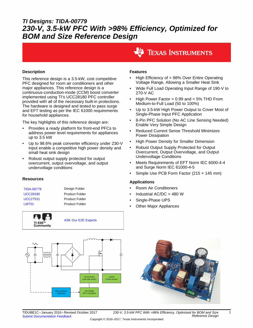
+ – UCC27531D (Low-side driver) UCC28180 (PFC controller) LMT01 (Temp sensor) Boost follower (Optional) 1 TIDUBE1C – January 2016 – Revised October 2017 Submit Documentation Feedback Copyright © 2016–2017, Texas Instruments Incorporated 230-V, 3.5-kW PFC With >98% Efficiency, Optimized for BOM and Size Reference Design TI Designs: TIDA-00779 230-V, 3.5-kW PFC With >98% Efficiency, Optimized for BOM and Size Reference Design Description This reference design is a 3.5-kW, cost competitive PFC designed for room air conditioners and other major appliances. This reference design is a continuous-conduction-mode (CCM) boost converter implemented using TI’s UCC28180 PFC controller provided with all of the necessary built-in protections. The hardware is designed and tested to pass surge and EFT testing as per the IEC 61000 requirements for household appliances. The key highlights of this reference design are: • Provides a ready platform for front-end PFCs to address power level requirements for appliances up to 3.5 kW • Up to 98.6% peak converter efficiency under 230-V input enable a competitive high power density and small heat sink design • Robust output supply protected for output overcurrent, output overvoltage, and output undervoltage conditions Resources TIDA-00779 Design Folder UCC28180 Product Folder UCC27531 Product Folder LMT01 Product Folder ASK Our E2E Experts Features • High Efficiency of > 98% Over Entire Operating Voltage Range, Allowing a Smaller Heat Sink • Wide Full Load Operating Input Range of 190-V to 270-V AC • High Power Factor > 0.99 and < 5% THD From Medium-to-Full Load (50 to 100%) • Up to 3.5-kW High Power Output to Cover Most of Single-Phase Input PFC Application • 8-Pin PFC Solution (No AC Line Sensing Needed) Enable Very Simple Design • Reduced Current Sense Threshold Minimizes Power Dissipation • High Power Density for Smaller Dimension • Robust Output Supply Protected for Output Overcurrent, Output Overvoltage, and Output Undervoltage Conditions • Meets Requirements of EFT Norm IEC 6000-4-4 and Surge Norm IEC 61000-4-5 • Simple Use PCB Form Factor (215 × 145 mm) Applications • Room Air Conditioners • Industrial AC/DC > 480 W • Single-Phase UPS • Other Major Appliances

Welcome message from author
This document is posted to help you gain knowledge. Please leave a comment to let me know what you think about it! Share it to your friends and learn new things together.
Transcript
+±
UCC27531D(Low-side driver)
UCC28180(PFC controller)
LMT01(Temp sensor)
Boost follower(Optional)
1TIDUBE1C–January 2016–Revised October 2017Submit Documentation Feedback
Copyright © 2016–2017, Texas Instruments Incorporated
230-V, 3.5-kW PFC With >98% Efficiency, Optimized for BOM and SizeReference Design
TI Designs: TIDA-00779230-V, 3.5-kW PFC With >98% Efficiency, Optimized forBOM and Size Reference Design
DescriptionThis reference design is a 3.5-kW, cost competitivePFC designed for room air conditioners and othermajor appliances. This reference design is acontinuous-conduction-mode (CCM) boost converterimplemented using TI’s UCC28180 PFC controllerprovided with all of the necessary built-in protections.The hardware is designed and tested to pass surgeand EFT testing as per the IEC 61000 requirementsfor household appliances.
The key highlights of this reference design are:• Provides a ready platform for front-end PFCs to
address power level requirements for appliancesup to 3.5 kW
• Up to 98.6% peak converter efficiency under 230-Vinput enable a competitive high power density andsmall heat sink design
• Robust output supply protected for outputovercurrent, output overvoltage, and outputundervoltage conditions
Resources
TIDA-00779 Design FolderUCC28180 Product FolderUCC27531 Product FolderLMT01 Product Folder
ASK Our E2E Experts
Features• High Efficiency of > 98% Over Entire Operating
Voltage Range, Allowing a Smaller Heat Sink• Wide Full Load Operating Input Range of 190-V to
270-V AC• High Power Factor > 0.99 and < 5% THD From
Medium-to-Full Load (50 to 100%)• Up to 3.5-kW High Power Output to Cover Most of
Single-Phase Input PFC Application• 8-Pin PFC Solution (No AC Line Sensing Needed)
Enable Very Simple Design• Reduced Current Sense Threshold Minimizes
Power Dissipation• High Power Density for Smaller Dimension• Robust Output Supply Protected for Output
Overcurrent, Output Overvoltage, and OutputUndervoltage Conditions
• Meets Requirements of EFT Norm IEC 6000-4-4and Surge Norm IEC 61000-4-5
• Simple Use PCB Form Factor (215 × 145 mm)
Applications• Room Air Conditioners• Industrial AC/DC > 480 W• Single-Phase UPS• Other Major Appliances

System Description www.ti.com
2 TIDUBE1C–January 2016–Revised October 2017Submit Documentation Feedback
Copyright © 2016–2017, Texas Instruments Incorporated
230-V, 3.5-kW PFC With >98% Efficiency, Optimized for BOM and SizeReference Design
An IMPORTANT NOTICE at the end of this TI reference design addresses authorized use, intellectual property matters and otherimportant disclaimers and information.
1 System DescriptionMajor appliance equipment such as air conditioners, refrigerators, and washers use three-phase, pulse-width modulated BLDC or PMSM drives. These motor drives typically have fractional or low horsepowerratings ranging from 0.25 HP (186 W) to 5 HP (3.75 kW). An electronic drive is required to control thestator currents in a BLDC or PMSM motor. A typical electronic drive consists of:• Power stage with a three-phase inverter with the required power capability• Microcontroller unit (MCU) to implement the motor control algorithm• Motor voltage and current sensing for closed-loop speed or torque control• Gate driver for driving the three-phase inverter• Power supply to power up the gate driver and MCU
These drives require a front-end power PFC regulator to shape the input current of the power supply andto meet the standards for power factor and current THD, such as IEC61000-2-3. A PFC circuit shapes theinput current of the power supply to be in phase with the mains voltage and helps to maximize the realpower drawn from the mains. The front-end PFC also offers several benefits:• Reduces RMS input current
For instance, a power circuit with a 230-V/5-A rating is limited to about 575 W of available power with apower factor (PF) of 0.5. Increasing the PF to 0.99 almost doubles the deliverable power to 1138 W,allowing the operation of higher power loads.
• Facilitates power supply hold-upThe active PFC circuit maintains a fixed, intermediate DC bus voltage that is independent of the inputvoltage so that the energy stored in the system does not decrease as the input voltage decreases. Thismaintenance allows the use of smaller, cost effective bulk capacitors.
• Improves efficiency of downstream convertersThe PFC reduces the dynamic voltage range applied to the downstream inverters and converters. As aresult, the voltage ratings of rectifiers can be reduced, resulting in lower forward drops. The operatingduty cycle can also be increased, resulting in lower current in the switches.
This reference design is a boost PF regulator implemented using the UCC28180 device as a PFCcontroller for use in all appliances that demand a PF correction of up to 3.5 kW. The design provides aready platform of an active front-end to operate downstream inverters or DC/DC converters operating on ahi-line AC voltage range from 190-V to 270-V AC.
This design demonstrates a high power density PF stage in a small form factor (215 × 145 mm) thatoperates from 190-V to 270-V AC and delivers up to 3.5 kW of continuous power output to drive invertersor converters at more than a 98% efficiency rate without an SiC device. This TI Design also providesflexibility for the boost follower configuration, in which the boost voltage can be varied with AC inputvoltage, but only can work on the boosted voltage when it is above the peak input voltage. The boostfollower configuration helps reduce switching losses in the PFC regulator and the downstream inverter orconverter. This design also gave an efficiency comparison in using MOSFET and IGBT, which can helpcustomer to choose efficiency or cost is preferred.
Above all, this TI Design meets the key challenges of appliances to provide safe and reliable power withall protections built in while delivering a high performance with low power consumption and a verycompetitive bill-of material (BOM) cost.

www.ti.com System Description
3TIDUBE1C–January 2016–Revised October 2017Submit Documentation Feedback
Copyright © 2016–2017, Texas Instruments Incorporated
230-V, 3.5-kW PFC With >98% Efficiency, Optimized for BOM and SizeReference Design
1.1 Key System Specifications
Table 1. Key System Specifications
PARAMETER SYMBOL TEST CONDITIONS MIN NOM MAX UNITINPUT CHARACTERISTICSInput voltage VIN — 85 230 270 V ACFrequency FAC — 47 — 64 HzInput UVLO VIN_UVLO IOUT = nom — 80 — V ACPower factor PF VIN = nom, IOUT = max — 0.99 — —Input current IIN VIN = nom, IOUT = max — 20 — AOUTPUT CHARACTERISTICSOutput voltage VOUT VIN = nom, IOUT = min to max — 390 — VOutput current IOUT VIN = 190-V AC to max 0 — 9 AOutput power POUT VIN = 190-V AC to max — — 3.5 kWLine regulation VIN = min to max, IOUT = nom — — 2 %Load regulation VIN = nom, IOUT = min to max — — 3 %Output voltage ripple VOUT_RIPPLE VIN = nom, IOUT = max — — 17 VOutput overvoltage VOVP IOUT = min to max — — 430 VOutput overcurrent IOCP VIN = min to max 12 — — ASYSTEM CHARACTERISTICSSwitching frequency fSW — — 45 — kHzPeak efficiency ηPEAK VIN = max, IOUT = 4 A, test with MOSFET — — 98.6 %Operation temperature TNOM With air flow –25 — 65 °C
+±
UCC27531D(Low-side driver)
UCC28180(PFC controller)
LMT01(Temp sensor)
Boost follower(Optional)
System Overview www.ti.com
4 TIDUBE1C–January 2016–Revised October 2017Submit Documentation Feedback
Copyright © 2016–2017, Texas Instruments Incorporated
230-V, 3.5-kW PFC With >98% Efficiency, Optimized for BOM and SizeReference Design
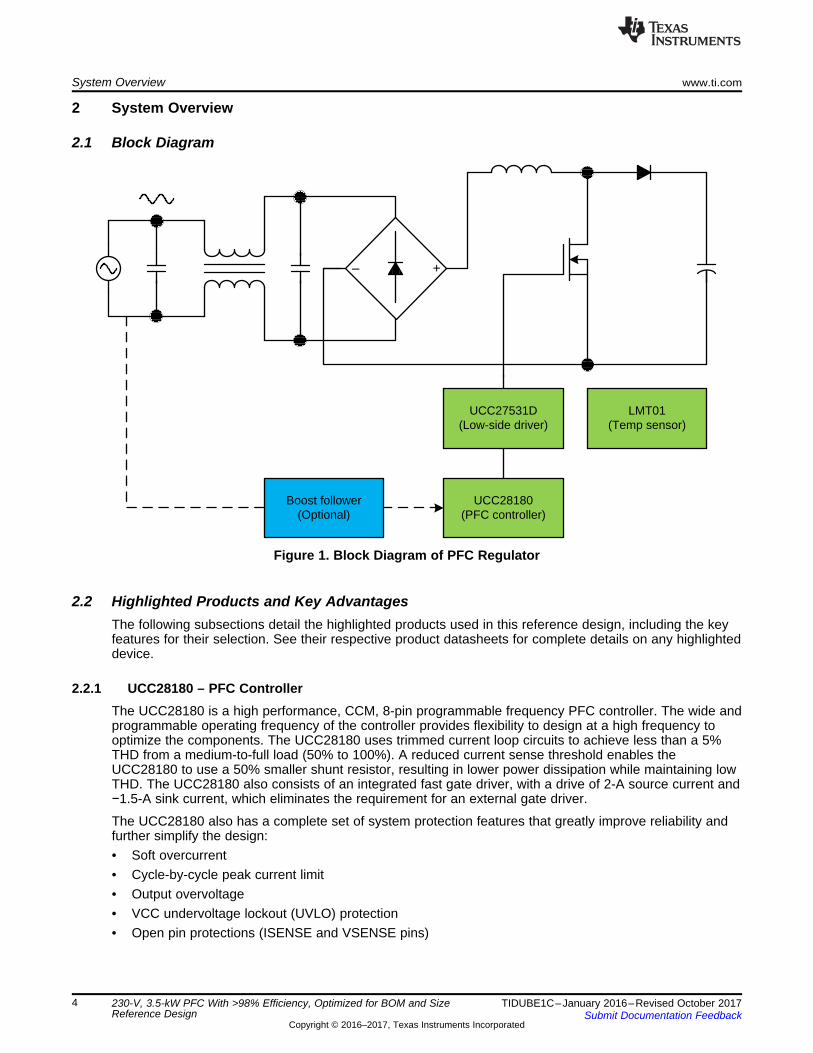
2 System Overview
2.1 Block Diagram
Figure 1. Block Diagram of PFC Regulator
2.2 Highlighted Products and Key AdvantagesThe following subsections detail the highlighted products used in this reference design, including the keyfeatures for their selection. See their respective product datasheets for complete details on any highlighteddevice.
2.2.1 UCC28180 – PFC ControllerThe UCC28180 is a high performance, CCM, 8-pin programmable frequency PFC controller. The wide andprogrammable operating frequency of the controller provides flexibility to design at a high frequency tooptimize the components. The UCC28180 uses trimmed current loop circuits to achieve less than a 5%THD from a medium-to-full load (50% to 100%). A reduced current sense threshold enables theUCC28180 to use a 50% smaller shunt resistor, resulting in lower power dissipation while maintaining lowTHD. The UCC28180 also consists of an integrated fast gate driver, with a drive of 2-A source current and−1.5-A sink current, which eliminates the requirement for an external gate driver.
The UCC28180 also has a complete set of system protection features that greatly improve reliability andfurther simplify the design:• Soft overcurrent• Cycle-by-cycle peak current limit• Output overvoltage• VCC undervoltage lockout (UVLO) protection• Open pin protections (ISENSE and VSENSE pins)
www.ti.com System Overview
5TIDUBE1C–January 2016–Revised October 2017Submit Documentation Feedback
Copyright © 2016–2017, Texas Instruments Incorporated
230-V, 3.5-kW PFC With >98% Efficiency, Optimized for BOM and SizeReference Design
2.2.2 UCC27531D – Low-Side Gate DriverObtaining a lower level of switching losses is important to achieve high efficiency. The switching losses ofa MOSFET are a function of the drive current that is required to quickly pass through the Miller plateauregion of the power-MOSFET's switching transition. Placing a high-current gate driver close to a FETallows for a faster turn on and turnoff by effectively charging and discharging voltage across theMOSFET’s gate-to-drain parasitic capacitor (CGD). This placement effectively reduces switching losses.
The UCC27531D is a single-channel, high-speed gate driver can effectively drive MOSFET and IGBTpower switch. Using a design that allows for a source of up to 2.5 A and a 5-A sink through asymmetricaldrive (split outputs), coupled with the ability to support a negative turn-off bias, rail-to-rail drive capability,extremely small propagation delay (17 ns typical), the UCC27531D are ideal solutions for MOSFET andIGBT power switches. The UCC27531D can also support enable, dual input, and inverting and non-inverting input functionality. The split outputs and strong asymmetrical drive boost the devices immunityagainst parasitic Miller turn-on effect and can help reduce ground debouncing.
Other key features that make the device ideal for this application are:• Wide VDD range from 10 to 35 V• Input and enable pins capable of withstanding up to –5-V DC below ground• UVLO• Output held low when input pins are floating or during VDD UVLO
Using an additional gate driver is an optional means to further reduce the switching losses because theUCC28180 controller has an integrated fast gate driver of 2-A source current and −1.5-A sink current,which is sufficient for this design.
2.2.3 LMT01 — Temperature SensorThe LMT01 is a high-accuracy, 2-pin temperature sensor with an easy-to-use pulse count interface, whichmakes it an ideal digital replacement for PTC or NTC thermistors both on and off board in industrial andconsumer markets. The LMT01 digital pulse count output and high accuracy over a wide temperaturerange allow pairing with any MCU without concern for integrated ADC quality or availability, whileminimizing software overhead. The LMT01 achieves flat ±0.5°C accuracy with very fine resolution(0.0625°C) over a wide temperature range of –20°C to 90°C without system calibration or hardware orsoftware compensation.
Unlike other digital IC temperature sensors, the LMT01’s single-wire interface is designed to directlyinterface with a GPIO or comparator input, thereby simplifying hardware implementation. Similarly, theLMT01's integrated EMI suppression and simple 2-pin architecture make it ideal for onboard and off-boardtemperature sensing. The LMT01 offers all the simplicity of analog NTC or PTC thermistors with the addedbenefits of a digital interface, wide specified performance, EMI immunity, and minimum processorresources. This design uses the LMT01 as the temperature monitor for the MOSFET or IGBT.
Other key features that make the device ideal for this application are:• Communication frequency: 88 kHz• Continuous conversion plus data-transmission period: 100 ms• Conversion current: 34 μA• Floating 2- to 5.5-V (VP–VN) supply operation with integrated EMI immunity

O
2 3500C 2286 F
390 50 50
´= = m
p ´ ´ ´
LOAD
O
O O LINE
2 PC
V V f
´=
p ´ ´ D ´
( ) ( ) ( )FREQ
65 kHz 32.7 k 1MR 47.9 k
45 kHz 1M 45 kHz 32.7 k 65 kHz 32.7 k
´ W ´ W= = W
´ W + ´ W - ´ W
( ) ( )TYP TYP INT
FREQ
SW INT TYP SW TYP TYP
f R RR
f R R f (R f )
´ ´=
´ + ´ - ´
System Overview www.ti.com
6 TIDUBE1C–January 2016–Revised October 2017Submit Documentation Feedback
Copyright © 2016–2017, Texas Instruments Incorporated
230-V, 3.5-kW PFC With >98% Efficiency, Optimized for BOM and SizeReference Design
2.3 System Design TheoryThis reference design is a 3.5-kW boost PFC regulator that operates in continuous conduction mode andis implemented using the UCC28180 PFC controller. The design is specifically tailored for inverter feddrives for use in major appliances such as air conditioners. This design serves as a simple and superioralternative to existing bulk, passive PFC circuits that are used to meet the power harmonic standards. Thesystem efficiency is greater than 98% over the wide input operating voltage range from 190-V to 270-V ACunder full load conditions. Additionally, this design includes several embedded protections including outputovervoltage protection and output short circuit protection.
The main focus of this design is a high efficiency, high PF, and protected DC power rail for targetedapplications.
2.3.1 Selecting Switching FrequencyThe UCC28180 switching frequency is user programmable with a single resistor on the FREQ pin to GND.
This design uses a 45-kHz switching frequency. Calculate the suitable resistor value to program theswitching frequency using Equation 1:
(1)
where• fTYP, RTYP, and RINT are constants internally fixed to the controller that are based on the UCC28180
control logic• fTYP = 65 kHz• RTYP = 32.7 kΩ• RINT = 1 MΩ
Applying these constants in Equation 2 yields the appropriate resistor that must be placed between theFREQ and GND pins.
(2)
A typical value of 47 kΩ for the FREQ resistor results in a switching frequency of 44 kHz.
2.3.2 Calculating Output CapacitanceAssuming that the percentage of non-conducting period is minimal, the required output capacitance canbe calculated as Equation 3 shows:
(3)
Where• ΔVO = The peak-to-peak voltage ripple on the output• fLINE = The input line frequency• PLOAD = The output load power
Insert the values into Equation 3 to obtain the following result:space
A capacitance of 2040 µF has been selected to accommodate overload conditions and effects caused byaging.

IN_MIN MINMIN 3
PK SW
2 V D 2 190 0.31L 174 H
I 0.4 f 26.6 0.4 45 10
´ ´ ´ ´³ = = m
´ ´ ´ ´ ´
OPK
IN_MIN
2 P 2 3500I 26.6 A
V 0.98 190
´ ´= = =
h ´ ´
( )IN_MIN LINE
MINO
2 V sin 2 f t 2 190 1D 1 0.31
V 390
´ ´ p ´ ´ ´ ´= - = =
www.ti.com System Overview
7TIDUBE1C–January 2016–Revised October 2017Submit Documentation Feedback
Copyright © 2016–2017, Texas Instruments Incorporated
230-V, 3.5-kW PFC With >98% Efficiency, Optimized for BOM and SizeReference Design
2.3.3 Calculating PFC Choke InductorThe UCC28180 is a CCM controller; however, if the chosen inductor allows a relatively high ripple current,the converter becomes forced to operate in discontinuous mode (DCM) at light loads and at the higherinput voltage range. High-inductor ripple current affects the CCM/DCM boundary and results in a higherlight-load THD. This type of current also affects the choices for the input capacitor, RSENSE, and CICOMPvalues. Allowing an inductor ripple current, ΔIRIPPLE, of 20% or less enables the converter to operate inCCM over the majority of the operating range. However, this low-inductor ripple current requires a boostinductor that has a higher inductance value, and the inductor itself is physically large. This design takescertain measures to optimize performance with size and cost. The inductor is sized to have a 40% peak-to-peak ripple current with a focus on minimizing space and the knowledge that the converter operates inDCM at the higher input voltages and at light loads; however, the converter is well optimized for a nominalinput voltage of 230-V AC at the full load.
Calculate the minimum value of the duty cycle, DMIN, as Equation 4 shows:
(4)
Based upon the allowable inductor ripple current of 40%, the PFC choke inductor, LBST, is selected afterdetermining the maximum inductor peak current, IPK, as Equation 5 shows:
(5)
Calculate the minimum value of the c, LMIN, based upon the acceptable ripple current, IRIPPLE, as Equation 6shows:
(6)
The actual value of the PFC choke inductor used is LMIN = 180 μH
2.3.4 Selecting Switching ElementThe MOSFET switch is driven by a gate output that is clamped at 15.2 V internally for VCC bias voltagesgreater than 15.2 V. An external gate drive resistor is recommended to limit the rise time and to dampenany ringing caused by the parasitic inductances and capacitances of the gate drive circuit. This resistoralso helps by meeting any EMI requirements of the converter. This design uses a 22-Ω resistor; the finalvalue of any design depends on the parasitic elements associated with the layout of the design. Tofacilitate a fast turnoff, place a standard 100-V, 1-A Schottky diode or switching diode anti-parallel with thegate drive resistor. A 10-kΩ resistor is placed between the gate of the MOSFET and ground to dischargethe gate capacitance and protect from inadvertent dV/dT triggered activations.
The maximum voltage across the FET is the maximum output boost voltage (that is, 425 V), which is theovervoltage set point of the PFC converter used to shut down the output. Considering a voltage de-ratingof 30%, the voltage rating of the MOSFET must be greater than 550-V DC.
This design uses an IPW60R099P6 MOSFET of 600 V with 37.9 A at 25°C and 24 A at 100°C. If cost is aconcern, this design also can use an IGBT (FGA4060ADF) to replace the MOSFET. This design needs aheat sink of the appropriate size for the MOSFET or IGBT.

System Overview www.ti.com
8 TIDUBE1C–January 2016–Revised October 2017Submit Documentation Feedback
Copyright © 2016–2017, Texas Instruments Incorporated
230-V, 3.5-kW PFC With >98% Efficiency, Optimized for BOM and SizeReference Design
2.3.5 Boost Follower Control CircuitThe traditional design of PFC boost converters consists of a fixed output voltage greater than themaximum peak line voltage to maintain boost operation and be able to shape the input current waveformof the power supply. The boost voltage does not have to be fixed, but can be varied based on the ACinput voltage provided that the boosted voltage is above the peak input voltage. The boost follower controlcircuit aids in setting the output voltage based on the peak input voltage.
Varying the output voltage with variations in the peak line voltage provides several benefits.• Reduced boost inductor
The boost inductor is selected based on the maximum allowed ripple current, at maximum duty cycle,at minimum line voltage, and at minimum output voltage. A decrease in VOUT results in a decrease inthe maximum duty cycle, which causes the boost inductor to decrease.
• Reduced boost switch losses at low line operationIn an offline PFC converter, a large amount of converter power loss is due to the switching losses ofthe boost FET. The boost follower PFC has a much lower output voltage at the low-input line voltagethan a traditional PFC boost, which reduces the switching losses.
• Reduced switching losses in the downstream inverter stage and isolated DC/DC converter stageThe switching losses in a three-phase inverter drive or isolated DC/DC converter stage are proportionalto the boost regulated voltage. A lower output voltage results in lower switching losses, increasing theoverall efficiency of the system, which is more noticeable in the light-load efficiency of the power stage.
2.3.6 Bias PowerThe TIDA-00779 design requires an external bias supply to power the UCC28180 PFC controllerUCC27531D gate driver, and relay, which is used to shunt the inrush current limiting resistor.
TI recommends powering these devices from a regulated auxiliary supply. These devices are not intendedto be used from a bootstrap bias supply. A bootstrap bias supply is fed from the input high voltage througha resistor with sufficient capacitance on the VCC pin to hold the voltage on the VCC pin until the currentcan be supplied from a bias winding on the boost inductor.
The UCC28180 has a UVLO of 11.5 V and the UCC27531D has a UVLO of 4.5 V, whereas the minimumvoltage required to turn on the relay is 9.6 V (for a 12-V relay), so the bias voltage for board operationmust be ≥ 12 V. The total current required for these devices is approximately 55 mA.
TI recommends using an external bias power supply of 12 V per 60 mA to power the board independently.The board has been tested and validated with a 12-V bias supply.

www.ti.com Hardware, Testing Requirements, and Test Results
9TIDUBE1C–January 2016–Revised October 2017Submit Documentation Feedback
Copyright © 2016–2017, Texas Instruments Incorporated
230-V, 3.5-kW PFC With >98% Efficiency, Optimized for BOM and SizeReference Design
3 Hardware, Testing Requirements, and Test Results
3.1 Required Hardware
3.1.1 Test ConditionsFor the input, the power supply source (VIN) must range from 190-V to 270-V AC. Set the input currentlimit of the input AC source to 25 A.
For the output, use an electronic variable load or a variable resistive load, which must be rated for ≥ 400 Vand must vary the load current from 0 mA to 10 A.
3.1.2 Recommended EquipmentUse the following recommended test equipment:• Fluke 287C (multimeter)• Chroma 61605 (AC source)• Chroma 63204 (DC electronic load)• Voltech PM100 / WT210 (power analyzer)• Tektronix DPO 3054 (oscilloscope)
3.1.3 Procedure
1. Connect input terminals (P1 and P2) of the reference board to the AC power source.2. Connect output terminals (P4 and P5) to the electronic load, maintaining correct polarity (P4 is the 390-
V DC output and P5 is the GND terminal).3. Connect an auxiliary supply of 12 V between pin-3 and pin-4 of connector J3, maintaining correct
polarity (pin-3 is the bias supply positive input and pin-4 is the GND terminal).4. Turn on the auxiliary supply and set a voltage of 12 V.5. Gradually increase the input voltage from 0 V to turn on the voltage of 190-V AC.6. To test the board independently, short pin-3 and pin-5 of connector J3.7. Turn on the load to draw current from the output terminals of the PFC.8. Observe the startup conditions for smooth-switching waveforms.

Hardware, Testing Requirements, and Test Results www.ti.com
10 TIDUBE1C–January 2016–Revised October 2017Submit Documentation Feedback
Copyright © 2016–2017, Texas Instruments Incorporated
230-V, 3.5-kW PFC With >98% Efficiency, Optimized for BOM and SizeReference Design
3.2 Test ResultsThe following test results cover the steady-state performance measurements, functional performance waveforms and test data, transientperformance waveforms, thermal measurements, surge measurements, and EFT measurements.
3.2.1 Performance Data
3.2.1.1 Efficiency and Regulation With Load VariationTable 2, Table 3, and Table 4 show the data at inputs of 190-V AC, 230-V AC, and 270-V AC input in using MOSFET and an ultra-fast diode.
Table 2. Performance Data With MOSFET and Ultra-Fast Diode Under 190-V AC Input
VINAC (V) IINAC (A) PINAC (W) PF THDi (%) VOUT (V) IOUT (A) POUT (W) EFFICIENCY (%) REG (%)190 0.60 81.7 0.716 15.82 392.8 0.20 78.2 95.68 0190 0.97 165.9 0.901 11.94 392.7 0.41 160.7 96.84 –0.03190 1.35 244.6 0.953 3.37 392.6 0.61 237.8 97.20 –0.05190 1.75 323.1 0.971 5.07 392.6 0.80 314.9 97.45 –0.05190 2.16 402.0 0.980 6.19 392.6 1.00 392.5 97.63 –0.05190 4.25 801.0 0.991 4.55 392.6 2.00 784.8 97.98 –0.05190 6.39 1202.0 0.990 3.28 392.6 3.00 1177.7 97.98 –0.05190 8.54 1599.0 0.986 3.19 392.7 3.99 1565.8 97.92 –0.03190 10.75 2003.0 0.981 3.35 392.9 4.99 1959.7 97.84 0.03190 12.83 2419.4 0.993 1.64 392.9 6.02 2365.3 97.76 0.03190 14.95 2822.7 0.994 1.76 393.0 7.02 2757.3 97.68 0.05190 17.06 3225.4 0.995 2.62 393.0 8.01 3147.9 97.60 0.05190 18.14 3435.1 0.996 2.39 393.1 8.52 3350.0 97.52 0.08

www.ti.com Hardware, Testing Requirements, and Test Results
11TIDUBE1C–January 2016–Revised October 2017Submit Documentation Feedback
Copyright © 2016–2017, Texas Instruments Incorporated
230-V, 3.5-kW PFC With >98% Efficiency, Optimized for BOM and SizeReference Design
Table 3. Performance Data With MOSFET and Ultra-Fast Diode Under 230-V AC Input
VINAC (V) IINAC (A) PINAC (W) PF THDi (%) VOUT (V) IOUT (A) POUT (W) EFFICIENCY (%) REG (%)230 0.62 81.3 0.569 18.74 392.3 0.20 77.2 94.96 –0.05230 0.90 165.6 0.802 22.51 392.3 0.41 160.2 96.75 –0.05230 1.18 244.4 0.901 10.20 392.3 0.61 237.6 97.21 –0.05230 1.49 322.4 0.941 6.39 392.3 0.80 314.8 97.65 –0.05230 1.82 401.2 0.960 3.54 392.3 1.00 392.4 97.81 –0.05230 3.52 799.0 0.987 4.88 392.3 2.00 784.6 98.20 –0.05230 5.26 1198.0 0.990 4.00 392.4 3.00 1177.7 98.31 –0.03230 7.00 1592.0 0.989 3.65 392.5 3.99 1565.4 98.33 0230 8.78 1994.0 0.987 3.63 392.6 4.99 1958.5 98.22 0.03230 10.56 2406.9 0.991 1.67 392.6 6.02 2363.8 98.21 0.03230 12.30 2808.6 0.993 1.87 392.7 7.02 2755.2 98.10 0.05230 14.04 3208.3 0.994 2.21 392.7 8.01 3145.9 98.06 0.05230 15.78 3612.3 0.995 2.40 392.8 9.01 3537.6 97.93 0.08
Table 4. Performance Data With MOSFET and Ultra-Fast Diode Under 270-V AC Input
VINAC (V) IINAC (A) PINAC (W) PF THDi (%) VOUT (V) IOUT (A) POUT (W) EFFICIENCY (%) REG (%)270 0.72 81.5 0.421 44.76 392.3 0.20 76.9 94.39 –0.05270 0.92 165.3 0.663 40.20 392.3 0.41 159.9 96.76 –0.05270 1.13 243.8 0.801 29.18 392.4 0.61 237.4 97.38 –0.03270 1.34 321.8 0.886 16.68 392.4 0.80 314.7 97.80 –0.03270 1.60 400.3 0.927 7.87 392.4 1.00 392.4 98.02 –0.03270 3.02 797.0 0.978 4.84 392.4 2.00 784.6 98.45 –0.03270 4.48 1195.0 0.988 4.61 392.4 3.00 1177.6 98.54 –0.03270 5.94 1588.0 0.990 4.17 392.5 3.99 1565.4 98.57 0270 7.43 1987.0 0.990 4.10 392.6 4.99 1958.5 98.57 0.03270 8.96 2399.2 0.992 1.99 392.6 6.02 2363.5 98.51 0.03270 10.43 2798.1 0.993 2.06 392.6 7.02 2754.5 98.44 0.03270 11.92 3198.5 0.994 2.35 392.7 8.01 3145.5 98.34 0.05270 13.41 3599.4 0.994 2.51 392.7 9.01 3536.7 98.26 0.05

Hardware, Testing Requirements, and Test Results www.ti.com
12 TIDUBE1C–January 2016–Revised October 2017Submit Documentation Feedback
Copyright © 2016–2017, Texas Instruments Incorporated
230-V, 3.5-kW PFC With >98% Efficiency, Optimized for BOM and SizeReference Design
Table 5 shows the data at a 230-V AC input in using an IGBT and an ultra-fast diode.
Table 5. Performance Data With IGBT and Ultra-Fast Diode Under 230-V AC Input
VINAC (V) IINAC (A) PINAC (W) PF THDi (%) VOUT (V) IOUT (A) POUT (W) EFFICIENCY (%) REG (%)230 0.55 45.0 0.354 16.39 392.5 0.10 41.1 91.33 –0.05230 1.95 409.3 0.914 8.34 392.5 1.01 398.4 97.34 –0.06230 3.61 807.2 0.971 5.86 392.4 2.01 790.0 97.87 –0.07230 5.32 1206.2 0.985 3.90 392.5 3.01 1182.1 98.00 –0.05230 7.09 1616.4 0.991 3.65 392.5 4.03 1584.8 98.04 –0.05230 8.83 2017.6 0.993 3.63 392.7 5.02 1977.8 98.03 –0.01230 10.58 2419.1 0.994 2.64 392.6 6.02 2369.6 97.95 –0.02230 12.34 2823.2 0.995 1.86 392.8 7.02 2764.0 97.90 0.04230 14.10 3227.3 0.995 2.47 392.8 8.01 3155.9 97.79 0.03230 15.88 3637.1 0.996 2.24 393.3 9.00 3551.9 97.66 0.15

www.ti.com Hardware, Testing Requirements, and Test Results
13TIDUBE1C–January 2016–Revised October 2017Submit Documentation Feedback
Copyright © 2016–2017, Texas Instruments Incorporated
230-V, 3.5-kW PFC With >98% Efficiency, Optimized for BOM and SizeReference Design
3.2.1.2 Efficiency and Regulation With Line VariationTable 6 and Table 7 show the data for the efficiency and line regulation of the output with AC input voltagevariation in using a MOSFET.
Table 6. Performance Data With Fixed Output Voltage in Using MOSFET
VINAC (V) IINAC (A) PINAC (W) PF VOUT (V) IOUT (A) POUT (W) EFFICIENCY (%)190 17.18 3247.7 0.995 392.9 8.01 3147.5 96.92200 16.52 3288.1 0.995 393.1 8.13 3193.9 97.14210 15.87 3316.6 0.995 393.2 8.21 3228.2 97.33220 15.33 3356.9 0.995 393.2 8.32 3273.0 97.50230 14.99 3432.6 0.996 393.3 8.52 3351.7 97.64240 14.68 3508.1 0.995 393.3 8.72 3429.6 97.76250 14.54 3619.1 0.996 393.2 9.00 3540.7 97.83260 13.97 3614.5 0.995 393.3 9.00 3540.8 97.96270 13.43 3610.5 0.996 393.3 9.00 3540.8 98.07
Table 7. Performance Data With Boost Follower Configuration in Using MOSFET
VINAC (V) IINAC (A) PINAC (W) PF VOUT (V) IOUT (A) POUT (W) EFFICIENCY (%)190 17.30 3267.6 0.994 333.1 9.51 3169.1 97.08200 16.75 3331.4 0.994 340.2 9.52 3240.1 97.26210 16.24 3392.2 0.995 347.2 9.52 3305.5 97.44220 15.76 3450.0 0.995 353.5 9.52 3366.0 97.56230 15.33 3508.5 0.995 360.0 9.52 3427.1 97.68240 14.95 3568.2 0.995 366.6 9.52 3489.2 97.79250 14.46 3597.0 0.995 373.2 9.43 3520.0 97.86260 13.81 3570.0 0.995 380.0 9.20 3496.8 97.95270 13.23 3552.6 0.995 386.9 9.00 3483.3 98.05

Hardware, Testing Requirements, and Test Results www.ti.com
14 TIDUBE1C–January 2016–Revised October 2017Submit Documentation Feedback
Copyright © 2016–2017, Texas Instruments Incorporated
230-V, 3.5-kW PFC With >98% Efficiency, Optimized for BOM and SizeReference Design
Table 8 and Table 9 show the data for the efficiency and line regulation of the output with AC input voltagevariation in using an IGBT.
Table 8. Performance Data With Fixed Output Voltage in Using IGBT
VINAC (V) IINAC (A) PINAC (W) PF VOUT (V) IOUT (A) POUT (W) EFFICIENCY (%)190 17.20 3253.0 0.995 392.8 8.01 3144.9 96.68200 16.55 3295.3 0.995 393.1 8.12 3192.8 96.89210 15.90 3324.4 0.995 393.3 8.21 3227.8 97.09220 15.36 3364.5 0.995 393.3 8.32 3272.6 97.27230 15.02 3439.9 0.996 393.3 8.52 3350.9 97.41240 14.71 3515.2 0.995 393.3 8.72 3428.7 97.54250 14.56 3625.3 0.996 393.2 9.00 3540.0 97.65260 13.98 3620.8 0.996 393.2 9.00 3540.0 97.77270 13.45 3616.2 0.996 393.2 9.00 3540.0 97.89
Table 9. Performance Data With Boost Follower Configuration in Using IGBT
VINAC (V) IINAC (A) PINAC (W) PF VOUT (V) IOUT (A) POUT (W) EFFICIENCY (%)190 17.05 3214.5 0.992 327.2 9.52 3113.6 96.86200 16.57 3290.6 0.993 335.5 9.52 3192.6 97.02210 16.12 3363.2 0.993 343.5 9.52 3267.9 97.17220 15.71 3435.0 0.994 351.4 9.52 3343.6 97.34230 15.32 3504.1 0.994 358.8 9.52 3414.4 97.44240 14.97 3571.7 0.994 366.2 9.52 3484.7 97.56250 14.51 3607.9 0.995 373.7 9.43 3524.0 97.67260 13.88 3589.1 0.995 381.4 9.20 3509.6 97.79270 13.31 3574.5 0.995 388.6 9.00 3498.6 97.88

Output Power (W)
Effi
cien
cy
0 500 1000 1500 2000 2500 3000 3500 400093%
94%
95%
96%
97%
98%
99%
D001
190-V AC230-V AC270-V AC
Output Power (W)
Effi
cien
cy
0 500 1000 1500 2000 2500 3000 3500 400096.5%
96.7%
96.9%
97.1%
97.3%
97.5%
97.7%
97.9%
98.1%
98.3%
98.5%
D004
IGBTMOSFET
www.ti.com Hardware, Testing Requirements, and Test Results
15TIDUBE1C–January 2016–Revised October 2017Submit Documentation Feedback
Copyright © 2016–2017, Texas Instruments Incorporated
230-V, 3.5-kW PFC With >98% Efficiency, Optimized for BOM and SizeReference Design
3.2.1.3 No Load PowerThe no load power was noted at multiple AC input voltages with the PFC controller enabled. Table 10 andTable 11 show the tabulated results with the fixed output and boost follower configuration.
Table 10. No Load Power With Fixed Output
VINAC (VAC) IINAC (mA) PINAC (W) VOUT (V) POUT (W) NO LOAD POWER (W)120 260.0 2.3 389.5 0.69 1.61150 320.0 2.4 389.5 0.69 1.71180 379.0 2.3 389.5 0.69 1.61230 476.0 2.3 389.5 0.69 1.61270 557.0 2.5 389.5 0.69 1.81
Table 11. No Load Power With Boost Follower Configuration
VINAC (VAC) IINAC (mA) PINAC (W) VOUT (V) POUT (W) NO LOAD POWER (W)120 259.0 1.3 292.0 0.39 0.91150 317.0 1.4 315.7 0.45 0.95180 377.0 1.6 336.1 0.51 1.09230 477.0 2.3 370.3 0.62 1.68270 558.0 2.6 397.7 0.72 1.88
3.2.2 Performance Curves
3.2.2.1 Efficiency CurvesFigure 2, Figure 3, Figure 4, and Figure 5 show the measured efficiency in the system with AC inputvoltage variation with and without boost follower configurations. These graphs also compare the efficiencyimprovement between using a MOSFET and using an IGBT.
Figure 2. Efficiency With Load Variation in UsingMOSFET
Figure 3. Efficiency Compared Between MOSFET andIGBT

Output Power (W)
Pow
er F
acto
r
0 500 1000 1500 2000 2500 3000 3500 40000.3
0.4
0.5
0.6
0.7
0.8
0.9
1
1.1
D002
190-V AC230-V AC270-V AC
Output Power (W)
TH
Di
0 500 1000 1500 2000 2500 3000 3500 40000.25%
1.25%
2.25%
3.25%
4.25%
5.25%
6.25%
7.25%
8.25%
9.25%
D003
190-V AC230-V AC270-V AC
Input Voltage (VAC)
Effi
cien
cy
180 200 220 240 260 28096.5%
96.7%
96.9%
97.1%
97.3%
97.5%
97.7%
97.9%
98.1%
98.3%
D005
Boost FollowerFixed Output
Input Voltage (VAC)
Effi
cien
cy
180 200 220 240 260 28096.5%
96.7%
96.9%
97.1%
97.3%
97.5%
97.7%
97.9%
98.1%
D006
Boost FollowerFixed Output
Hardware, Testing Requirements, and Test Results www.ti.com
16 TIDUBE1C–January 2016–Revised October 2017Submit Documentation Feedback
Copyright © 2016–2017, Texas Instruments Incorporated
230-V, 3.5-kW PFC With >98% Efficiency, Optimized for BOM and SizeReference Design
Figure 4. Efficiency versus AC Input Voltage in UsingMOSFET
Figure 5. Efficiency Versus AC Input Voltage in UsingIGBT
3.2.2.2 PF and THDi CurvesFigure 6 and Figure 7 show the measured PF value and THDi in the system with load variation.
Figure 6. Power Factor With Load Variation Figure 7. THDi With Load Variation

www.ti.com Hardware, Testing Requirements, and Test Results
17TIDUBE1C–January 2016–Revised October 2017Submit Documentation Feedback
Copyright © 2016–2017, Texas Instruments Incorporated
230-V, 3.5-kW PFC With >98% Efficiency, Optimized for BOM and SizeReference Design
3.2.3 Functional Waveforms
3.2.3.1 Startup and Shutdown Waveform
Figure 8. Start-up With Fixed Output Under 230-V ACInput
Figure 9. Shutdown With Fixed Output Under 230-V ACInput
Figure 10. Input Voltage versus Input Current Under HalfLoad
Figure 11. Input Voltage versus Input Current Under FullLoad

Hardware, Testing Requirements, and Test Results www.ti.com
18 TIDUBE1C–January 2016–Revised October 2017Submit Documentation Feedback
Copyright © 2016–2017, Texas Instruments Incorporated
230-V, 3.5-kW PFC With >98% Efficiency, Optimized for BOM and SizeReference Design
3.2.3.2 Inrush Current WaveformFigure 12 and Figure 13 show the inrush current drawn by the system. The inrush current was observedand recorded at a input voltage of 230-V and 270-V AC.
Figure 12. Inrush Current Under 230-V AC Input With NoLoad
Figure 13. Inrush Current Under 270-V AC Input With NoLoad
3.2.3.3 Input Voltage and Current WaveformFigure 14 and Figure 15 show the input current waveform at 230-V AC with a half and full-load condition.
Figure 14. Input Voltage and Current With Half LoadUnder 230-V AC Input
Figure 15. Input Voltage and Current With Full LoadUnder 230-V AC Input

www.ti.com Hardware, Testing Requirements, and Test Results
19TIDUBE1C–January 2016–Revised October 2017Submit Documentation Feedback
Copyright © 2016–2017, Texas Instruments Incorporated
230-V, 3.5-kW PFC With >98% Efficiency, Optimized for BOM and SizeReference Design
3.2.3.4 Output RippleAs Figure 16 and Figure 17 show, the ripple was observed at a 390-V DC output with half load and fullload, respectively.
Figure 16. Bus Voltage Ripple Under Half Load Figure 17. Bus Voltage Ripple Under Full Load
3.2.3.5 Switching Node WaveformFigure 18, Figure 19, Figure 20, and Figure 21 show the waveforms at the switching node, which wereobserved along with the MOSFET and IGBT for 230-V AC under full-load conditions.
Figure 18. VDS1, VDS2, and PFC Choke Current(MOSFET)
Figure 19. VGS1 and VGS2 (MOSFET)
Figure 20. Turn on of VGS1 and VGS2 (IGBT) Figure 21. Turn off of VGS1 and VGS2 (IGBT)

Hardware, Testing Requirements, and Test Results www.ti.com
20 TIDUBE1C–January 2016–Revised October 2017Submit Documentation Feedback
Copyright © 2016–2017, Texas Instruments Incorporated
230-V, 3.5-kW PFC With >98% Efficiency, Optimized for BOM and SizeReference Design
3.2.3.6 Transient WaveformThe load transient performance was observed with the load switched at a 0.2-m wire length. The outputload is switched using an electronic load.
Figure 22 and Figure 23 show the load transient waveforms for VIN = 230-V AC and a step load transientfrom 0.5 A to 8 A. Figure 22 shows a step change from 0.5 A to 8 A, and Figure 23 shows a load stepdown from 8 A to 0.5 A.
Figure 22. DC Link Voltage versus DC Link CurrentUnder 0.5 A to 8 A
Figure 23. DC Link Voltage versus DC Link CurrentUnder 8 A to 0.5 A

www.ti.com Hardware, Testing Requirements, and Test Results
21TIDUBE1C–January 2016–Revised October 2017Submit Documentation Feedback
Copyright © 2016–2017, Texas Instruments Incorporated
230-V, 3.5-kW PFC With >98% Efficiency, Optimized for BOM and SizeReference Design
3.2.4 Thermal MeasurementsTo better understand the temperature of power components and maximum possible operatingtemperature, the thermal images were plotted at room temperature (25°C) with a closed enclosure, noairflow, and at full-load conditions. The board was allowed to run for 30 minutes before capturing a thermalimage.
Figure 24 shows the temperature of power components at input voltage of 230-V AC with the 3.5-kWpower output.
Figure 24. Top-Side Temperatures at 230-V AC Input and 3.5-kW Output
GNDE
PGND
820pFC11
PGND
13.0k
R9
390 VDC9 Amps max
TP5
TP7
TP9
TP1
TP6
VCC
GND1
ICOMP2
ISENSE3
FREQ4
VCOMP5
VSENSE6
VCC7
GATE8
U1
UCC28180D45kHz
340kR8
332kR7
332kR6
BA
T5
4
D4
10.0kR1
275VRV1
TP8
300k
R28
1000pF
C21
D5
1N4148W-7-F
NOTES:LINE INPUT VOLTAGE: 156VRMS - 265VRMS, 47Hz - 63HzPEAK INPUT CURRENT: 30.0A
OUTPUT VOLTAGE: 390VDC nominalMAXIMUM OUTPUT POWER: 3500W
Q32N7002-7-F
Q2MMBT3906
10.0k
R15
6.8kR16
15.4
R18
10uFC19
VCC
PGND
PGND PGND
PFC SHUTDOWN CIRCUITPGND
12-15 VDC
PFC_ON
CURRENT LIMIT RESISTOR BYPASS CIRCUIT
BIAS
BIAS
PGND
1uFC17
D6
CG
RM
400
7-G
CG
RM
4007
-G
D7
10uFC20
3
1
2
Q4
BC
84
7C
LT
1G
PGNDPGND
13.7kR14
PGND
Vsense
Vsense
TP10
BOOST FOLLOWER CONTROL CIRCUIT
221R11
332kR21
340kR22
10.0kR23
BAT54D8
Heatsink HS1 for BR1,
PGND
Switch ON delay 0.2s
VDCBUS
221kR35
221kR34
221kR36
221kR37
PGND
VDCBUS
Bleeder Resistor to discharge outputWhen unit is turned-off
21
L1
029E1-001
1 2
34
L2
2.5 mH
D1 FFH30S60S
1
32 Q1
IPW
60
R09
9P
6
+1
AC2
AC3
-4
BR1
GBJ3508
BZX384-C12,115D9
10uFC25
221kR27
47.5kR31
PGND PGND PGND
340kR26
340kR25
1
2
HS1
TBD
D2
1N5406
RTN
680 uFC4
0.01R5
21.0kR38
ACsense
ACsense
NOTES:For Boost Follower Configuration:Populate R14 and Q4 and set R9 = 21.5kPopulate R5 = 0.2 Ohm
For Fixed Output Boost PFC configurationDo not populate R14 and Q4 and Set R9 = 13kDo not populate R5
1
23
Q5
2N7002-7-F
1 2
34
L3
2.5 mH
C82.2nF
BIA
S
10R13
1.00kR39
BAT54D10
PFC_ON
PFC_ON
332kR20
Recommended to use TIDA-00473 Design for Bias Supply Needs
PFC_ON
RLY-N
RLY-N
RLY-P
RLY-P
680 uFC5
680 uFC18
1
32 Q6
IPW
60
R09
9P
6
10.0kR42
22R404.7
R24
4.7R41
TP4
PGND
VCC
0.39 FμC13
8.2 FμC14
0.1 FμC16
1 FμC12
0.47 FμC24
2.2 FμC1
2.2 Fμ
C2
2.2 Fμ
C22
C92.2nF
C62.2nF
C72.2nF
C262.2nF
C232.2nF
1 2
34K1
HF105F-1/12DT-1HS
R2
B470N
100
R43
D3 FFH30S60S
0.01R4
2.7nFC15
3300pF
C1047.0kR12
62k
R29
62k
R30
62k
R32
62k
R33
10.0k
R19
6.8kR17
1 2S1
KCD3-101N
PGND
P1
L
P2
N
TP2
P3
E
1
P4
Q1,Q6,D1,D3
1
P5
ENA1
INA2
GND3
INB4
OUTB5
VDD6
OUTA7
ENB8
U2
UCC27531D220pF
C27
D12
PGND
1 Fμ
C28 D11MMDL914-TP
22R3
0
R44
NOTES:For UCC27531D Configuration:Populate R44=0 Ohm
For UCC27524A ConfigurationDo not populate R44
1 2
L4TP3
10.0kR10
0.01R45
1µFC3
F1
30A
NOTES:For MOSFET Configuration:Bias Power input by 12 VDC
For IGBT Configuration:Bias Power input by 15 VDC
5
4
1
2
3
6
J3
PEC06SAAN
VPVN
Design Files www.ti.com
22 TIDUBE1C–January 2016–Revised October 2017Submit Documentation Feedback
Copyright © 2016–2017, Texas Instruments Incorporated
230-V, 3.5-kW PFC With >98% Efficiency, Optimized for BOM and SizeReference Design
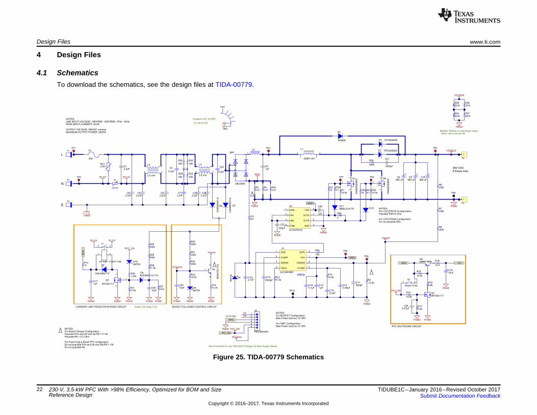
4 Design Files
4.1 SchematicsTo download the schematics, see the design files at TIDA-00779.
Figure 25. TIDA-00779 Schematics

www.ti.com Design Files
23TIDUBE1C–January 2016–Revised October 2017Submit Documentation Feedback
Copyright © 2016–2017, Texas Instruments Incorporated
230-V, 3.5-kW PFC With >98% Efficiency, Optimized for BOM and SizeReference Design
4.2 Bill of MaterialsTo download the bill of materials (BOM), see the design files at TIDA-00779.
4.3 Layout PrintsTo download the layout prints, see the design files at TIDA-00779.
4.4 Altium ProjectTo download the Altium project files, see the design files at TIDA-00779.
4.5 Gerber FilesTo download the Gerber files, see the design files at TIDA-00779.
4.6 Assembly DrawingsTo download the assembly drawings, see the design files at TIDA-00779.
5 References
1. Texas Instruments, 230-V, 900-W, Power Factor Regulator Converter (PFC) for Inverter-Fed Drivesand Appliances, TIDA-00443 Design Guide
2. Texas Instruments, Using the UCC28180EVM-573 360-W Power Factor Correction Module,UCC28180EVM-573 User’s Guide
3. Texas Instruments, UCC28180 Programmable Frequency, Continuous Conduction Mode (CCM), BoostPower Factor Correction (PFC) Controller, UCC28180 Datasheet
5.1 TrademarksAll trademarks are the property of their respective owners.
6 About the AuthorYUAN (JASON) TAO is a systems engineer at Texas Instruments, where he is responsible for developingreference design solutions for the industrial segment. Yuan brings to this role his extensive experience inpower electronics, high frequency DC/DC, AC/DC converters, and analog circuit design. Yuan earned hismaster of IC design and manufacture from Shanghai Jiao Tong University in 2007.

Revision History www.ti.com
24 TIDUBE1C–January 2016–Revised October 2017Submit Documentation Feedback
Copyright © 2016–2017, Texas Instruments Incorporated
Revision History
Revision HistoryNOTE: Page numbers for previous revisions may differ from page numbers in the current version.
Changes from B Revision (May 2016) to C Revision ...................................................................................................... Page
• Changed formatting to fit current design guide template............................................................................. 1• Changed THD from more than 5% to less than 5% .................................................................................. 1
Changes from A Revision (March 2016) to B Revision .................................................................................................. Page
• Changed title............................................................................................................................... 1
Changes from Original (January 2016) to A Revision .................................................................................................... Page
• Changed from preview page............................................................................................................. 1

IMPORTANT NOTICE FOR TI DESIGN INFORMATION AND RESOURCES
Texas Instruments Incorporated (‘TI”) technical, application or other design advice, services or information, including, but not limited to,reference designs and materials relating to evaluation modules, (collectively, “TI Resources”) are intended to assist designers who aredeveloping applications that incorporate TI products; by downloading, accessing or using any particular TI Resource in any way, you(individually or, if you are acting on behalf of a company, your company) agree to use it solely for this purpose and subject to the terms ofthis Notice.TI’s provision of TI Resources does not expand or otherwise alter TI’s applicable published warranties or warranty disclaimers for TIproducts, and no additional obligations or liabilities arise from TI providing such TI Resources. TI reserves the right to make corrections,enhancements, improvements and other changes to its TI Resources.You understand and agree that you remain responsible for using your independent analysis, evaluation and judgment in designing yourapplications and that you have full and exclusive responsibility to assure the safety of your applications and compliance of your applications(and of all TI products used in or for your applications) with all applicable regulations, laws and other applicable requirements. Yourepresent that, with respect to your applications, you have all the necessary expertise to create and implement safeguards that (1)anticipate dangerous consequences of failures, (2) monitor failures and their consequences, and (3) lessen the likelihood of failures thatmight cause harm and take appropriate actions. You agree that prior to using or distributing any applications that include TI products, youwill thoroughly test such applications and the functionality of such TI products as used in such applications. TI has not conducted anytesting other than that specifically described in the published documentation for a particular TI Resource.You are authorized to use, copy and modify any individual TI Resource only in connection with the development of applications that includethe TI product(s) identified in such TI Resource. NO OTHER LICENSE, EXPRESS OR IMPLIED, BY ESTOPPEL OR OTHERWISE TOANY OTHER TI INTELLECTUAL PROPERTY RIGHT, AND NO LICENSE TO ANY TECHNOLOGY OR INTELLECTUAL PROPERTYRIGHT OF TI OR ANY THIRD PARTY IS GRANTED HEREIN, including but not limited to any patent right, copyright, mask work right, orother intellectual property right relating to any combination, machine, or process in which TI products or services are used. Informationregarding or referencing third-party products or services does not constitute a license to use such products or services, or a warranty orendorsement thereof. Use of TI Resources may require a license from a third party under the patents or other intellectual property of thethird party, or a license from TI under the patents or other intellectual property of TI.TI RESOURCES ARE PROVIDED “AS IS” AND WITH ALL FAULTS. TI DISCLAIMS ALL OTHER WARRANTIES ORREPRESENTATIONS, EXPRESS OR IMPLIED, REGARDING TI RESOURCES OR USE THEREOF, INCLUDING BUT NOT LIMITED TOACCURACY OR COMPLETENESS, TITLE, ANY EPIDEMIC FAILURE WARRANTY AND ANY IMPLIED WARRANTIES OFMERCHANTABILITY, FITNESS FOR A PARTICULAR PURPOSE, AND NON-INFRINGEMENT OF ANY THIRD PARTY INTELLECTUALPROPERTY RIGHTS.TI SHALL NOT BE LIABLE FOR AND SHALL NOT DEFEND OR INDEMNIFY YOU AGAINST ANY CLAIM, INCLUDING BUT NOTLIMITED TO ANY INFRINGEMENT CLAIM THAT RELATES TO OR IS BASED ON ANY COMBINATION OF PRODUCTS EVEN IFDESCRIBED IN TI RESOURCES OR OTHERWISE. IN NO EVENT SHALL TI BE LIABLE FOR ANY ACTUAL, DIRECT, SPECIAL,COLLATERAL, INDIRECT, PUNITIVE, INCIDENTAL, CONSEQUENTIAL OR EXEMPLARY DAMAGES IN CONNECTION WITH ORARISING OUT OF TI RESOURCES OR USE THEREOF, AND REGARDLESS OF WHETHER TI HAS BEEN ADVISED OF THEPOSSIBILITY OF SUCH DAMAGES.You agree to fully indemnify TI and its representatives against any damages, costs, losses, and/or liabilities arising out of your non-compliance with the terms and provisions of this Notice.This Notice applies to TI Resources. Additional terms apply to the use and purchase of certain types of materials, TI products and services.These include; without limitation, TI’s standard terms for semiconductor products http://www.ti.com/sc/docs/stdterms.htm), evaluationmodules, and samples (http://www.ti.com/sc/docs/sampterms.htm).
Mailing Address: Texas Instruments, Post Office Box 655303, Dallas, Texas 75265Copyright © 2017, Texas Instruments Incorporated
Related Documents