2138 IEEE JOURNAL OF SOLID-STATE CIRCUITS, VOL. 44, NO. 8, AUGUST 2009 CMOS Oscillators for Clock Distribution and Injection-Locked Deskew Masum Hossain and Anthony Chan Carusone, Senior Member, IEEE Abstract—The distribution and alignment of high-frequency clocks across a wide bus of links is a significant challenge in modern computing systems. A low power clock source is demon- strated by incorporating a buffer into a cross-coupled oscillator. Because the load is isolated from the tank, the oscillator can directly drive 50-Ohm impedances or large capacitive loads with no additional buffering. Using this topology, a quadrature VCO (QVCO) is implemented in 0.13 m digital CMOS. The QVCO oscillates at 20 GHz, consumes 20 mW and provides 12% tuning range. The measured phase noise is dBc Hz @ 1 MHz frequency offset. A clock alignment technique based upon injec- tion-locked quadrature-LC or ring oscillators is then proposed. Although injection-locked oscillators (ILOs) are known to be capable of deskewing and jitter filtering clocks, a study of both LC and ring ILOs indicates significant variation in their jitter tracking bandwidth when used to provide large phase shifts. By selectively injecting different phases of a quadrature-LC or ring VCO, this problem is obviated resulting in reduced phase noise. The technique is demonstrated using a LC QVCO at 20 GHz while burning only 20 mW of power and providing an 8 dB improvement in phase noise. A ring oscillator deskews a 2 to 7 GHz clock while consuming 14 mW in 90 nm CMOS. Index Terms—Clock deskew, injection locking, jitter filtering, Q-VCO, ring oscillator. I. INTRODUCTION T HE energy efficiency of high-speed parallel I/Os is lim- ited by the power consumption of the clocking circuits including clock source, buffers, delay elements and duty cycle correctors. To reduce the power consumption per link, a shared clock source may be used where the phase of the VCO is locked to an external low-jitter [1], [2]. Due to the significant capaci- tive loading on the clock distribution network, several CML and CMOS inverters are used as buffers [3]. In this work, we pro- pose a VCO with an inherent buffer that re-uses the VCO bias current and provides large driving capacity without additional power consumption. Section II will discuss low power VCO architectures: Colpitts, cross-coupled and proposed VCO. Im- plementation and experimental results will also be given in this section. Manuscript received December 01, 2008; revised April 01, 2009. Current ver- sion published July 22, 2009. This work was supported by Intel. Fabrication services were provided by Gennum Corporation and Canadian Microelectronic Corporation (CMC). The authors are with the Department of Electrical and Computer Engi- neering, University of Toronto, Toronto, Ontario, Canada, M5S 3G4 (e-mail: [email protected]; [email protected]. Color versions of one or more of the figures in this paper are available online at http://ieeexplore.ieee.org. Digital Object Identifier 10.1109/JSSC.2009.2022917 Fig. 1. Shared clocking for high density I/O [1]–[4]. Each link’s receiver must compensate for the link’s skew with a deskew circuit [4], [5] (Fig. 1). Apart from phase alignment, the deksew block also provides amplification, duty cycle correc- tion and jitter filtering to recover high quality clock. An injec- tion locked oscillator (ILO) is an efficient way of providing all these functionalities; by detuning the oscillator’s free-running frequency away from the input frequency, a controlled phase shift is introduced to the clock path [6]. A problem with this ap- proach has been that for large phase shifts considerable varia- tion is observed in the jitter tracking bandwidth and output clock amplitude [7]. In this work, by selectively injecting either one or the other side of a quadrature VCO (QVCO), the required phase adjustment range is cut in half. Section III will provide some the- oretical ground work for ILO-based clock deskewing, demon- strating that the variation in jitter tracking bandwidth is funda- mental to both LC and ring ILOs. Following that, Section IV will discuss the deskew technique including experimental results for both LC and ring oscillators. II. LOW POWER VCO ARCHITECTURE We will first discuss two existing LC VCO topologies: cross- coupled and Colpitts. Finally, the proposed architecture which combines the benefit of both topologies will be discussed. A. Cross-Coupled Oscillator A cross-coupled LC VCO topology and its equivalent half cir- cuit is shown in Fig. 2. Here, the ideal gain of is furnished by the cross-coupling to provide a negative resistance of . The tank consists of an inductor and tunable capacitance . The tank loss is mainly dominated by the inductor series re- sistance which also determines the inductor quality factor . The series resistance can be converted to 0018-9200/$26.00 © 2009 IEEE Authorized licensed use limited to: Texas A M University. Downloaded on August 4, 2009 at 09:41 from IEEE Xplore. Restrictions apply.

Welcome message from author
This document is posted to help you gain knowledge. Please leave a comment to let me know what you think about it! Share it to your friends and learn new things together.
Transcript
2138 IEEE JOURNAL OF SOLID-STATE CIRCUITS, VOL. 44, NO. 8, AUGUST 2009
CMOS Oscillators for Clock Distribution andInjection-Locked Deskew
Masum Hossain and Anthony Chan Carusone, Senior Member, IEEE
Abstract—The distribution and alignment of high-frequencyclocks across a wide bus of links is a significant challenge inmodern computing systems. A low power clock source is demon-strated by incorporating a buffer into a cross-coupled oscillator.Because the load is isolated from the tank, the oscillator candirectly drive 50-Ohm impedances or large capacitive loads withno additional buffering. Using this topology, a quadrature VCO(QVCO) is implemented in 0.13 m digital CMOS. The QVCOoscillates at 20 GHz, consumes 20 mW and provides 12% tuningrange. The measured phase noise is ��� dBc Hz @ 1 MHzfrequency offset. A clock alignment technique based upon injec-tion-locked quadrature-LC or ring oscillators is then proposed.Although injection-locked oscillators (ILOs) are known to becapable of deskewing and jitter filtering clocks, a study of bothLC and ring ILOs indicates significant variation in their jittertracking bandwidth when used to provide large phase shifts. Byselectively injecting different phases of a quadrature-LC or ringVCO, this problem is obviated resulting in reduced phase noise.The technique is demonstrated using a LC QVCO at 20 GHz whileburning only 20 mW of power and providing an 8 dB improvementin phase noise. A ring oscillator deskews a 2 to 7 GHz clock whileconsuming 14 mW in 90 nm CMOS.
Index Terms—Clock deskew, injection locking, jitter filtering,Q-VCO, ring oscillator.
I. INTRODUCTION
T HE energy efficiency of high-speed parallel I/Os is lim-ited by the power consumption of the clocking circuits
including clock source, buffers, delay elements and duty cyclecorrectors. To reduce the power consumption per link, a sharedclock source may be used where the phase of the VCO is lockedto an external low-jitter [1], [2]. Due to the significant capaci-tive loading on the clock distribution network, several CML andCMOS inverters are used as buffers [3]. In this work, we pro-pose a VCO with an inherent buffer that re-uses the VCO biascurrent and provides large driving capacity without additionalpower consumption. Section II will discuss low power VCOarchitectures: Colpitts, cross-coupled and proposed VCO. Im-plementation and experimental results will also be given in thissection.
Manuscript received December 01, 2008; revised April 01, 2009. Current ver-sion published July 22, 2009. This work was supported by Intel. Fabricationservices were provided by Gennum Corporation and Canadian MicroelectronicCorporation (CMC).
The authors are with the Department of Electrical and Computer Engi-neering, University of Toronto, Toronto, Ontario, Canada, M5S 3G4 (e-mail:[email protected]; [email protected].
Color versions of one or more of the figures in this paper are available onlineat http://ieeexplore.ieee.org.
Digital Object Identifier 10.1109/JSSC.2009.2022917
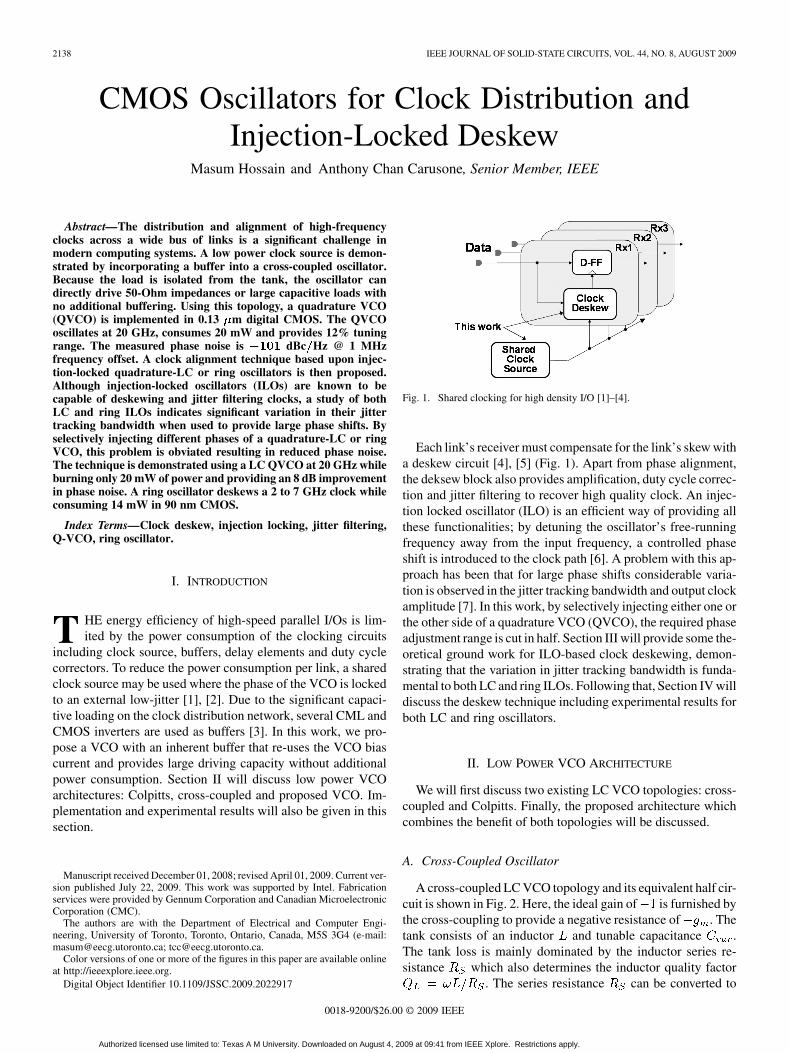
Fig. 1. Shared clocking for high density I/O [1]–[4].
Each link’s receiver must compensate for the link’s skew witha deskew circuit [4], [5] (Fig. 1). Apart from phase alignment,the deksew block also provides amplification, duty cycle correc-tion and jitter filtering to recover high quality clock. An injec-tion locked oscillator (ILO) is an efficient way of providing allthese functionalities; by detuning the oscillator’s free-runningfrequency away from the input frequency, a controlled phaseshift is introduced to the clock path [6]. A problem with this ap-proach has been that for large phase shifts considerable varia-tion is observed in the jitter tracking bandwidth and output clockamplitude [7]. In this work, by selectively injecting either one orthe other side of a quadrature VCO (QVCO), the required phaseadjustment range is cut in half. Section III will provide some the-oretical ground work for ILO-based clock deskewing, demon-strating that the variation in jitter tracking bandwidth is funda-mental to both LC and ring ILOs. Following that, Section IV willdiscuss the deskew technique including experimental results forboth LC and ring oscillators.
II. LOW POWER VCO ARCHITECTURE
We will first discuss two existing LC VCO topologies: cross-coupled and Colpitts. Finally, the proposed architecture whichcombines the benefit of both topologies will be discussed.
A. Cross-Coupled Oscillator
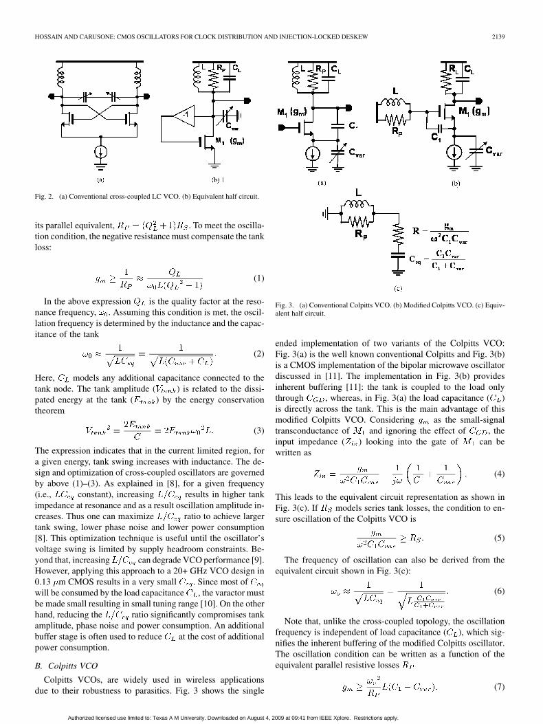
A cross-coupled LC VCO topology and its equivalent half cir-cuit is shown in Fig. 2. Here, the ideal gain of is furnished bythe cross-coupling to provide a negative resistance of . Thetank consists of an inductor and tunable capacitance .The tank loss is mainly dominated by the inductor series re-sistance which also determines the inductor quality factor
. The series resistance can be converted to
0018-9200/$26.00 © 2009 IEEE
Authorized licensed use limited to: Texas A M University. Downloaded on August 4, 2009 at 09:41 from IEEE Xplore. Restrictions apply.
HOSSAIN AND CARUSONE: CMOS OSCILLATORS FOR CLOCK DISTRIBUTION AND INJECTION-LOCKED DESKEW 2139
Fig. 2. (a) Conventional cross-coupled LC VCO. (b) Equivalent half circuit.
its parallel equivalent, . To meet the oscilla-tion condition, the negative resistance must compensate the tankloss:
(1)
In the above expression is the quality factor at the reso-nance frequency, . Assuming this condition is met, the oscil-lation frequency is determined by the inductance and the capac-itance of the tank
(2)
Here, models any additional capacitance connected to thetank node. The tank amplitude ( ) is related to the dissi-pated energy at the tank ( ) by the energy conservationtheorem
(3)
The expression indicates that in the current limited region, fora given energy, tank swing increases with inductance. The de-sign and optimization of cross-coupled oscillators are governedby above (1)–(3). As explained in [8], for a given frequency(i.e., constant), increasing results in higher tankimpedance at resonance and as a result oscillation amplitude in-creases. Thus one can maximize ratio to achieve largertank swing, lower phase noise and lower power consumption[8]. This optimization technique is useful until the oscillator’svoltage swing is limited by supply headroom constraints. Be-yond that, increasing can degrade VCO performance [9].However, applying this approach to a 20+ GHz VCO design in0.13 m CMOS results in a very small . Since most ofwill be consumed by the load capacitance , the varactor mustbe made small resulting in small tuning range [10]. On the otherhand, reducing the ratio significantly compromises tankamplitude, phase noise and power consumption. An additionalbuffer stage is often used to reduce at the cost of additionalpower consumption.
B. Colpitts VCO
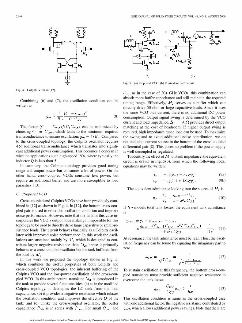
Colpitts VCOs, are widely used in wireless applicationsdue to their robustness to parasitics. Fig. 3 shows the single
Fig. 3. (a) Conventional Colpitts VCO. (b) Modified Colpitts VCO. (c) Equiv-alent half circuit.
ended implementation of two variants of the Colpitts VCO:Fig. 3(a) is the well known conventional Colpitts and Fig. 3(b)is a CMOS implementation of the bipolar microwave oscillatordiscussed in [11]. The implementation in Fig. 3(b) providesinherent buffering [11]: the tank is coupled to the load onlythrough , whereas, in Fig. 3(a) the load capacitance ( )is directly across the tank. This is the main advantage of thismodified Colpitts VCO. Considering as the small-signaltransconductance of and ignoring the effect of , theinput impedance ( ) looking into the gate of can bewritten as
(4)
This leads to the equivalent circuit representation as shown inFig. 3(c). If models series tank losses, the condition to en-sure oscillation of the Colpitts VCO is
(5)
The frequency of oscillation can also be derived from theequivalent circuit shown in Fig. 3(c):
(6)
Note that, unlike the cross-coupled topology, the oscillationfrequency is independent of load capacitance ( ), which sig-nifies the inherent buffering of the modified Colpitts oscillator.The oscillation condition can be written as a function of theequivalent parallel resistive losses
(7)
Authorized licensed use limited to: Texas A M University. Downloaded on August 4, 2009 at 09:41 from IEEE Xplore. Restrictions apply.
2140 IEEE JOURNAL OF SOLID-STATE CIRCUITS, VOL. 44, NO. 8, AUGUST 2009
Fig. 4. Colpitts VCO in [12].
Combining (6) and (7), the oscillation condition can bewritten as
(8)
The factor can be minimized bychoosing , which leads to the minimum requiredtransconductance to ensure oscillation: . Comparedto the cross-coupled topology, the Colpitts oscillator requires4 additional transconductance which translates into signifi-cant additional power consumption. This becomes a concern inwireline applications such high-speed I/Os, where typically theinductor Q is less than 5.
In summary, the Colpitts topology provides good tuningrange and output power but consumes a lot of power. On theother hand, cross-coupled VCOs consume less power, butrequire an additional buffer and are more susceptible to loadparasitics [13].
C. Proposed VCO
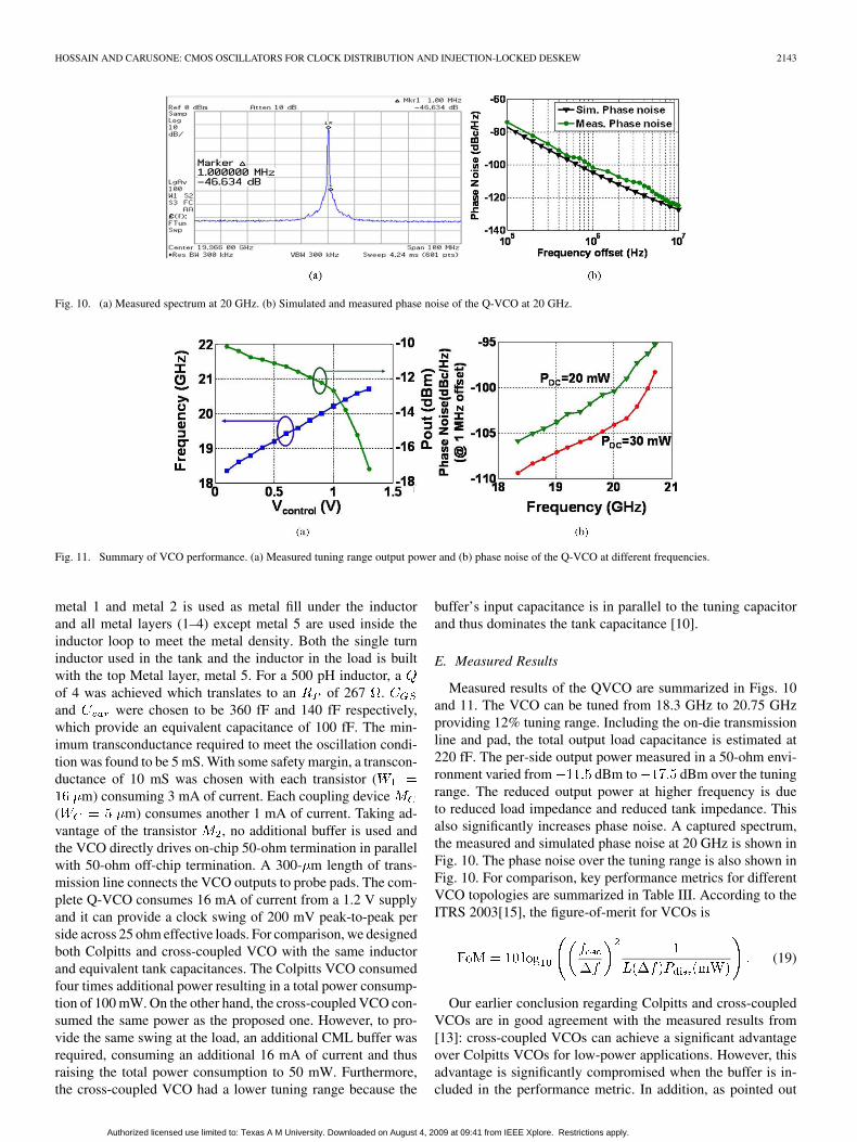
Cross-coupled and Colpitts VCOs have been previously com-bined in [12] as shown in Fig. 4. In [12], the bottom cross-cou-pled pair is used to relax the oscillation condition and improvenoise performance. However, note that the tank in this case in-corporates the VCO’s output node making it impossible for thistopology to be used to directly drive large capacitive or small-re-sistance loads. The circuit behaves basically as a Colpitts oscil-lator with improved noise performance. In this work the oscil-lations are sustained mainly by which is designed to con-tribute larger negative resistance than , hence it primarilybehaves as a cross-coupled oscillator but the tank buffered fromthe load by .
In this work we proposed the topology shown in Fig. 5,which combines the useful properties of both Colpitts andcross-coupled VCO topologies: the inherent buffering of theColpitts VCO and the low-power oscillation of the cross-cou-pled VCO. In this architecture, transistor is introduced inthe tank to provide several functionalities: (a) as in the modifiedColpitts topology, it decouples the LC tank from the loadcapacitance; (b) it provides a negative resistance which relaxesthe oscillation condition and improves the effective of thetank; and (c) unlike the cross-coupled oscillator, the buffercapacitance is in series with . For small and
Fig. 5. (a) Proposed VCO. (b) Equivalent half circuit.
, as in the case of 20+ GHz VCOs, this combination canabsorb more buffer capacitance and still maintain the requiredtuning range. Effectively, serves as a buffer which candirectly drive 50-ohm or large capacitive loads. Since it usesthe same VCO bias current, there is no additional DC powerconsumption. Output signal swing is determined by the VCOcurrent and load impedance. provides direct outputmatching at the cost of headroom. If higher output swing isrequired, high impedance tuned load can be used. To maximizethe swing and to avoid additional noise contribution, we donot include a current source in the bottom of the cross-coupleddifferential pair [8]. This poses no problem if the power supplyis well decoupled or regulated.
To identify the effect of on tank impedance, the equivalentcircuit is drawn in Fig. 5(b), from which the following nodalequations may be written:
(9a)
(9b)
The equivalent admittance looking into the source of is
(10)
If models total tank losses, the equivalent tank admittanceis
(11)
At resonance, the tank admittance must be real. Thus, the oscil-lation frequency can be found by equating the imaginary part tozero
(12)
To sustain oscillation at this frequency, the bottom cross-cou-pled transistors must provide sufficient negative resistance toovercome the tank losses
(13)
This oscillation condition is same as the cross-coupled casewith one additional factor: the negative resistance contributed by
, which allows additional power savings. Note that there are
Authorized licensed use limited to: Texas A M University. Downloaded on August 4, 2009 at 09:41 from IEEE Xplore. Restrictions apply.

HOSSAIN AND CARUSONE: CMOS OSCILLATORS FOR CLOCK DISTRIBUTION AND INJECTION-LOCKED DESKEW 2141
two sources of negative resistance here: the bottom cross-cou-pled pair provide a negative transconductance, and the toptransistors provide . As a result this os-cillator has two possible modes of operation: (i) as a ColpittsVCO, when the negative resistance provided by is suffi-cient to compensate the tank losses, similar to [12]; or (ii) asa cross-coupled VCO, when the negative resistance due todominates the oscillation condition. The cross-coupled modeof oscillation requires less power consumption, and hence isthe main focus of this work. In this configuration ischosen to provide sufficient tuning range and is sized suchthat its gate drain capacitance is small enough to isolate the tankfrom the output nodes. As a result, the negative resistance of thetop transistors is less than 30% of that contributed by the bottompair.
The effective quality factor ( ) for this equivalent tankcan be expressed as
(14)
It is useful to express this effective tank quality factor in termsof inductor quality factor .
(15)
Note that, in the absence of transistor , the tankquality factor is equal to the inductor quality factor. However,in the presence of , it is possible to improve the tank qualityfactor well beyond . For example, consider a 500 pH in-ductor with a quality factor of 4 used to design a 20 GHz VCO.Choosing and mS, we can im-prove the tank Q beyond 10, which results in a 2.5 improve-ment in tank swing. This is particularly useful when designingLC-VCOs in digital CMOS process, where the lossy substratelimits the inductor Q to approximately 4 or 5. For comparison,the proposed tank is simulated with and without as shown inFig. 6. Note that, the improvement in tank amplitude is a directeffect of the improved quality factor. Using similar approachas described in [14], oscillation amplitude can be derived fromFig. 5(b). In the current limited region, the single ended ampli-tude of the voltage across the inductor can be written as
(16)
(17)
Here, is the large signal effective transconductance ofthe transistor . The voltage across gate and source terminalof can be written as
(18)
Simulated oscillation amplitude is in good agreement (within15%) with these two expressions. The simulated phase noiseof this 20 GHz VCO at 1 MHz offset was dBc Hz. Themajor noise contributors are summarized in Table I. Simulation
Fig. 6. (a) Simulated tank with and without � . (b) Equivalent tankimpedance (magnitude and phase) over the tuning range.
TABLE IPHASE NOISE CONTRIBUTION OF EACH NOISE SOURCE
results also demonstrate that a 20% variation in is suf-ficient to provide greater than 10% tuning range. To study theeffectiveness of as a buffer, we observed the VCO perfor-mance over a large variation of load capacitance from 100 fF to1 pF. For m, the frequency variation is only 50 MHz,the phase noise variation is less than 0.5 dB, and the oscillationamplitude varies less than 3%. However, as we increase the sizeof , its effectiveness as a buffer degrades. As shown in Fig. 7,for m, a load capacitance variation from 100 fF to1 pF results in 200 MHz variation in frequency, 1.5 dB varia-tion in phase noise and 7% variation in oscillation amplitude.Variation in the value of from 10 to 70 ohm has even lesseffect than variations in . Larger values of will result inheadroom issues. A comparison of key VCO parameters for allthree topologies is summarized in Table II, which supports thequalitative discussion: the proposed VCO essentially combinesthe benefits of both the cross-coupled and Colpitts topologies.
D. QVCO Implementation
Three existing methods for generating quadrature clocksignals are: 1) a VCO followed by C-R, R-C filters, 2) adifferential VCO of twice the frequency followed by rising-and falling-edge trigged dividers, and 3) a Q-VCO formed bycoupling two differential VCOs. The first technique resultsin significant additional power consumption in the buffersdriving the passive filter. The second technique requires thedesign of a 40 GHz VCO and dividers in 0.13 m digitalCMOS which would be difficult and power consuming. Thus
Authorized licensed use limited to: Texas A M University. Downloaded on August 4, 2009 at 09:41 from IEEE Xplore. Restrictions apply.

2142 IEEE JOURNAL OF SOLID-STATE CIRCUITS, VOL. 44, NO. 8, AUGUST 2009
Fig. 7. Effect of load capacitance variation on (a) oscillation frequency and (b) phase noise.
Fig. 8. Implementation of QVCO architecture, test set up and detail schematic of QVCO.
TABLE IIVCO TOPOLOGY SUMMARY
for quadrature signal generation at 20 GHz, we focus on thethird approach: a Q-VCO. A quadrature version of the pro-posed VCO is implemented by coupling two differential VCOsoperating at the same frequency. In-phase coupling, with acoupling factor greater than 0.25, ensures quadrature phasegeneration. Coupling was provided using additional devices
(Fig. 8). Quadrature (4-phase) VCOs in general haveseveral disadvantages compared to their differential (2-phase)counterparts: a) due to the additional DC power consumptionin the coupling devices, the power consumption of a quadratureVCO is usually more than twice the power consumption of adifferential VCO at the same frequency; b) in the quadratureimplementation, both tanks operate slightly off resonance dueto mismatch which results in higher phase noise and reducedtank impedance compared to a differential implementation.
This QVCO is implemented in 0.13 m digital CMOS, typ-ical for high speed I/Os (Fig. 9). There were five metal layersavailable with the top layer being less than 1 m thick. Poly, Fig. 9. Die photo of the implemented Q-VCO in 0.13 �m CMOS.
Authorized licensed use limited to: Texas A M University. Downloaded on August 4, 2009 at 09:41 from IEEE Xplore. Restrictions apply.
HOSSAIN AND CARUSONE: CMOS OSCILLATORS FOR CLOCK DISTRIBUTION AND INJECTION-LOCKED DESKEW 2143
Fig. 10. (a) Measured spectrum at 20 GHz. (b) Simulated and measured phase noise of the Q-VCO at 20 GHz.
Fig. 11. Summary of VCO performance. (a) Measured tuning range output power and (b) phase noise of the Q-VCO at different frequencies.
metal 1 and metal 2 is used as metal fill under the inductorand all metal layers (1–4) except metal 5 are used inside theinductor loop to meet the metal density. Both the single turninductor used in the tank and the inductor in the load is builtwith the top Metal layer, metal 5. For a 500 pH inductor, aof 4 was achieved which translates to an of 267 .and were chosen to be 360 fF and 140 fF respectively,which provide an equivalent capacitance of 100 fF. The min-imum transconductance required to meet the oscillation condi-tion was found to be 5 mS. With some safety margin, a transcon-ductance of 10 mS was chosen with each transistor (
m) consuming 3 mA of current. Each coupling device( m) consumes another 1 mA of current. Taking ad-vantage of the transistor , no additional buffer is used andthe VCO directly drives on-chip 50-ohm termination in parallelwith 50-ohm off-chip termination. A 300- m length of trans-mission line connects the VCO outputs to probe pads. The com-plete Q-VCO consumes 16 mA of current from a 1.2 V supplyand it can provide a clock swing of 200 mV peak-to-peak perside across 25 ohm effective loads. For comparison, we designedboth Colpitts and cross-coupled VCO with the same inductorand equivalent tank capacitances. The Colpitts VCO consumedfour times additional power resulting in a total power consump-tion of 100 mW. On the other hand, the cross-coupled VCO con-sumed the same power as the proposed one. However, to pro-vide the same swing at the load, an additional CML buffer wasrequired, consuming an additional 16 mA of current and thusraising the total power consumption to 50 mW. Furthermore,the cross-coupled VCO had a lower tuning range because the
buffer’s input capacitance is in parallel to the tuning capacitorand thus dominates the tank capacitance [10].
E. Measured Results
Measured results of the QVCO are summarized in Figs. 10and 11. The VCO can be tuned from 18.3 GHz to 20.75 GHzproviding 12% tuning range. Including the on-die transmissionline and pad, the total output load capacitance is estimated at220 fF. The per-side output power measured in a 50-ohm envi-ronment varied from dBm to dBm over the tuningrange. The reduced output power at higher frequency is dueto reduced load impedance and reduced tank impedance. Thisalso significantly increases phase noise. A captured spectrum,the measured and simulated phase noise at 20 GHz is shown inFig. 10. The phase noise over the tuning range is also shown inFig. 10. For comparison, key performance metrics for differentVCO topologies are summarized in Table III. According to theITRS 2003[15], the figure-of-merit for VCOs is
(19)
Our earlier conclusion regarding Colpitts and cross-coupledVCOs are in good agreement with the measured results from[13]: cross-coupled VCOs can achieve a significant advantageover Colpitts VCOs for low-power applications. However, thisadvantage is significantly compromised when the buffer is in-cluded in the performance metric. In addition, as pointed out
Authorized licensed use limited to: Texas A M University. Downloaded on August 4, 2009 at 09:41 from IEEE Xplore. Restrictions apply.

2144 IEEE JOURNAL OF SOLID-STATE CIRCUITS, VOL. 44, NO. 8, AUGUST 2009
TABLE IIICOMPARISON OF STATE-OF-ART CMOS VCOS
in the previous section, there is significant performance degra-dation in cross-coupled QVCOs compared to their differentialcounterparts [16], [17]. Although the inductor Q in this VCOis much lower compared to the other VCOs listed in the table,this VCO topology still has a FoM better than other QVCOsin CMOS. The differential 10 GHz Colpitts VCO designed in[13] consumes more power than the 20 GHz QVCO designedin this work, which demonstrates the low power advantage ofthe proposed topology. The current consumption of the QVCOis set by the gate voltage of transistor . Keeping the samesupply voltage of 1.2 V, power consumption can be increasedfrom 20 mW to 30 mW which results in 5 dB reduction in phasenoise (Fig. 11).
III. DESKEW WITH INJECTION LOCKING
Historically, injection locking has been used for low powerfrequency division [18]. More recently, ILOs are also used as ajitter filter on high-frequency clocks [19] and as a clock deskewelement [6], [7]. Compared to traditional voltage-control delayelements, ILO-based deskew provides several advantages:(a) due to its high sensitivity, ILOs can operate with very smallinput amplitude – thus the reference clock can be distributedwith low power; (b) since an ILO behaves as a first order PLL,it rejects high frequency jitter and is less susceptible to powersupply noise; (c) the clock can be deskewed by detuning thefree running frequency of the ILO. To cover an entire clockperiod, the required deskew range should be at least .Assuming that phase-inversion of a differential ILO may betrivially accommodated, a deskew range of is required.
Present ILO-based deskew techniques have several disadvan-tages. For small injected signals, the deskew range is less than
[7]. With large injection strength, it is possible to extendthe deskew range but this requires a wide tuning range in theILO. Furthermore, providing skews near 90 results in consid-erable variation in the jitter tracking bandwidth and output clock
Fig. 12. ILO model and corresponding vector diagram.
amplitude [7]. Previous theoretical studies on ILOs have fo-cused on their lock range and the behavior of an ILO outside itslock range for both small injection [20] and large injection [21].In this work we are specifically interested in the phase noise(and jitter) of the deskewed clock. We seek a general treatmentapplicable to both LC and ring VCOs.
With that motivation, we adopt the ILO model shown inFig. 12 for any injection method and oscillator topology [18],[21]. Here, is the VCO’s small-signal open loop fre-quency response and will depend on the VCO topology. In thecase of an LC oscillator, is a tuned response, whereas,in case of a ring oscillator, is a low pass response.Nonlinearities associated with the VCOs are taken into accountby the nonlinear block. The phasor diagram in Fig. 12 is takenwith respect to the injected frequency, . The oscillator hasa free running frequency of . Under injection within the os-cillator’s lock range, the oscillator output frequency drifts from
and, in steady-state, settles to . Let its instantaneousoscillation frequency be and is the inherent frequencydifference, . Thus, the oscillator outputphasor rotates with an instantaneous angularfrequency . The phasor is the vector summation of
and : . Here, is thephase shift introduced by the to satisfy the oscillationcondition, . It was shown in [21] that
(20)
Authorized licensed use limited to: Texas A M University. Downloaded on August 4, 2009 at 09:41 from IEEE Xplore. Restrictions apply.

HOSSAIN AND CARUSONE: CMOS OSCILLATORS FOR CLOCK DISTRIBUTION AND INJECTION-LOCKED DESKEW 2145
where is the injection strength. We define
(21)
By noting and substituting ,this may be rearranged
(22)
Equating from (20) and (22),
(23)
This is the same locking equation used in [20] and [21], butgeneralized so that all oscillator-topology dependence is cap-tured by . For the parallel RLC resonant tank [20], [21],
(24)
where is the quality factor of the tank circuit. For an LC res-onant tank with resistive losses in series with the inductor, theappropriate value of is [22]
(25)
A simpler definition of may be obtained by taking a first-order expansion of around in (18). Since isthe oscillator’s free-running frequency, at .Hence,
(26)
The accuracy of this approximation diminishes as in-creases. For a ring oscillator, this approximation is used in theAppendix to show that
(27)
where is the number of stages in the ring. With these expres-sions for , we can use (23) as a general locking equation whichis VCO topology-independent.
A. Clock Deskew
Within the lock range, the steady state output frequency willalways track the injected frequency, , and the phasedifference between the injected and ILO output becomes con-stant, . Making these substitutions into (23),
(28)
where is the steady state phase shift between the injectedand output clocks. The maximum value of is obtained when
. Thus, we define lock range as
(29)
Within lock range (28) is valid for any valueof and . For small injection strength i.e.,the above relation can be simplified as [20]
(30)
As (30) suggests, for small frequency offsets the phase shift isapproximately linear with respect to . This property is partic-ularly useful for ILO-based clock deskewing. Experimental andsimulated deskew curves using the differential VCO topologydiscussed in the previous section are shown in Fig. 13. For ex-perimental study we AC coupled an external 19 GHz clock toI-VCO only. Deskew curve was generated by detuning I – VCOonly. According to (30), the deskew angle decreases withincreasing injection strength . Note that the validity of (30) islimited to small injection strength ( ) only. For larger injectionstrength we can consider (29) where we see that the lock rangeincreases with injection strength. In particular, larger injectionstrength increases the usable linear portion of the deskew curve,
vs. . Finally, note that (30) predicts a maximum achiev-able achievable deskew of ; however, under very stronginjection the approximations in (30) break down and slightlylarger deskew angles are, in fact, achievable but accompaniedby nonlinearity in the deskew curve and, as we shall see, varia-tions in the jitter tracking bandwidth and oscillation amplitude.
B. Phase Noise Filtering
The transient phase response of the ILO can be obtained byintegrating (23) with respect to time resulting in a first-orderresponse [20], [21]
(31)
In (31), is the phase difference at time between thefree running VCO output and the injected clock. Generalizingthe result in [18] to cover different oscillator topologies, canbe estimated as
(32)
For weak injection, , this simplifies to the same resultas in [20], [21], . Thus, ILOs are functionally equiv-alent to a first order PLL [18] where input phase noise is lowpass filtered
(33)
and VCO phase noise is high pass filtered
(34)
Authorized licensed use limited to: Texas A M University. Downloaded on August 4, 2009 at 09:41 from IEEE Xplore. Restrictions apply.

2146 IEEE JOURNAL OF SOLID-STATE CIRCUITS, VOL. 44, NO. 8, AUGUST 2009
Fig. 13. (a) Captured deskewed clock at different skew setting. (b) Skew curve as a function of free running VCO frequency (� � �� � 19 GHz).
Fig. 14. (a) Simulated and predicted phase noise of the LC VCO at different deskew settings at � � �� � 19 GHz. (b) Simulated and predicted jitter transfercharacteristics at different skew settings � � �� � 19 GHz. For both simulations � � � and � � ����.
Here is the jitter frequency. If is the phase noise ofthe injected signal and is the VCO phase noise, then thephase noise of the deskewed clock is
(35)
Using the jitter transfer functions in (33) and (34),
(36)
It is also desirable to express the phase noise of the deskewedclock as a function of deskew angle . This can be done usingthe relationship between frequency offset and deskew angle:
(37)
This phase noise expression for the deskewed clock providesseveral insights: (a) the jitter tracking bandwidth of the ILOdepends upon the frequency offset between the injected and
free running VCO frequency, , and hence upon the deskewangle, ; (b) Close to the lock range ( ),
, so no phase noise filtering will be observed. Taking adifferent approach, the same conclusion was obtained in [23].In terms of the phase shift, , effective phase noise filtering isachieved for small deskew angles, but for large deskew angles(e.g., ) no phase noise filtering is achievable (i.e.,
).The LC VCO discussed in Section II is simulated as an ILO
by injecting a relatively low-jitter clock into the tank through acapacitive coupling. The injected clock frequency was 19 GHzand the free-running VCO frequency was detuned away from19 GHz to obtain phase shifts. The predicted phase noise ofthe deskewed clock along with the simulated one is shown inFig. 14(a). For this study a low noise clock is generated and in-jected to the differential VCO. Normalized jitter transfer func-tions are shown for different deskew angles in Fig. 14(b). JitterTracking Bandwidth (JTB) of the ILO as a function of the fre-quency offset and injection strength is shown in Fig. 15. The the-oretical predictions are based upon a parallel RLC-tank modelusing the expression for in (21) with . For small phaseshifts, the theory and simulation results are in good agreement.Increasing discrepancies are observed at larger phase shifts be-cause of the simplified parallel RLC-tank model. Regardless, at
very little jitter filtering is observed. This was also
Authorized licensed use limited to: Texas A M University. Downloaded on August 4, 2009 at 09:41 from IEEE Xplore. Restrictions apply.
HOSSAIN AND CARUSONE: CMOS OSCILLATORS FOR CLOCK DISTRIBUTION AND INJECTION-LOCKED DESKEW 2147
Fig. 15. Variation of jitter tracking bandwidth (JTB) as a function of frequency offset and injection strength, � � �� � 19 GHz and � � �.
Fig. 16. Measured phase noise plot of the VCO, injected signal and deskewedclock at � � �� � 19 GHz.
experimentally verified by capturing phase noise plots of the in-jected signal, free-running VCO, and the deskewed clock underinjection locking in Fig. 16.
C. Deskew With Harmonic Injection
Phase deskew can also be achieved when the VCO is injectedwith a super- or sub-harmonic clock such that .The phase noise expression in (33) becomes,
(38)If the oscillator is injected with th order sub-harmonic, then
the output phase noise will degrade by a factor within thejitter tracking bandwidth [24]. On the other hand, super-har-monic injection improves the phase noise of the injected signalby . For example, second harmonic of the oscillation fre-quency is injected in the tail of the four stage ring oscillatorin Fig. 17(a). The phase noise of the deskewed clock and thecorresponding jitter tracking bandwidth at different deskew an-gles is shown in Fig. 17(b)-(c) and compared with theoreticalpredictions based upon (38), the expression for derived in the
Appendix . Again theoretical predictions are in good agreementwith the simulation results for small deskew phase angles. Forlarge phase shifts, inaccuracies arise due to first-order approxi-mation for applied in (23).
In summary, the theory, simulation and experimental study ofthe ILO-based deskew techniques have identified several limi-tations of existing techniques for large phase deskew angles: (i)the phase steps are non-linear; (ii) the output clock amplitudevaries significantly and (iii) there is little or no jitter filtering.However, if we restrict the frequency offset within
, above-mentioned limitations are not very signif-icant. The derived phase noise expressions are applicable forany ILO topology with appropriate choice of . The theoret-ical results are summarized for both ring and LC oscillators inTable IV.
IV. PROPOSED DESKEW TECHNIQUE
In the proposed architecture, a QVCO is used, where we canselectively inject either the in-phase or the quadrature portion ofthe VCO. This allows us to achieve using only half of thelock range. As a result, both jitter tracking bandwidth and clockamplitude suffers much less variation. This proposed techniquecan be implemented either with an LC QVCO or using a ringoscillator.
A. Deskew With LC QVCO
The analysis of a differential ILO can be extended for aquadrature ILO as shown in Fig. 18. First we will study thecase without injection and then, the effect of injection will bediscussed. Due to mutual coupling between the two VCOs, eachof them oscillates at a frequency slightly offset from resonance.As a result, in a free running QVCO the tank introduces a phaseshift between the output voltage and current .Thus the mutual coupling between these two VCOs can beviewed as injection locking [25] and the general locking (23)can be applied to both the I-VCO and Q-VCO:
(39)
(40)
Authorized licensed use limited to: Texas A M University. Downloaded on August 4, 2009 at 09:41 from IEEE Xplore. Restrictions apply.
2148 IEEE JOURNAL OF SOLID-STATE CIRCUITS, VOL. 44, NO. 8, AUGUST 2009
Fig. 17. Deskew with harmonic injection locking. (a) Implemented ring oscillator for deskew. (b) Phase noise at different skew settings at � � �� � 14 GHz(b) Jitter transfer characteristics at different skew setting � � �� � 14 GHz. For both simulations � � ����, � � �, � � �� � 7 GHz and � � ���.
TABLE IVSUMMARY OF ILO BASED DESKEW PARAMETERS
Here, we assume that both VCOs are identical (i.e., )and the phase difference between them is ( ).To find the final phase relationship between these two VCOs,we find the steady-state solution of the above equations:
(41)
To further simplify the above equations, we consider two cases:1) Case : I: , when two loops are strongly coupled, :
(42) Fig. 18. Proposed phase deskew technique. (a) Q VCO model without injec-tion. (b) QVCO with injection for proposed deskew scheme.
Authorized licensed use limited to: Texas A M University. Downloaded on August 4, 2009 at 09:41 from IEEE Xplore. Restrictions apply.
HOSSAIN AND CARUSONE: CMOS OSCILLATORS FOR CLOCK DISTRIBUTION AND INJECTION-LOCKED DESKEW 2149
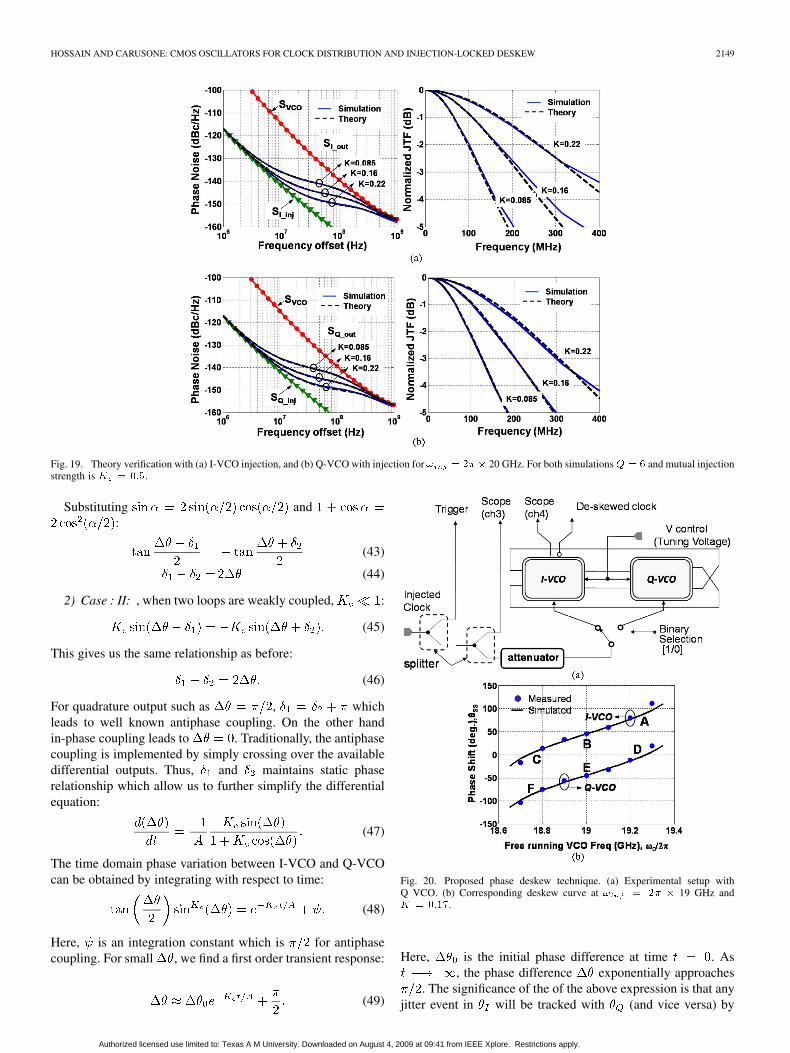
Fig. 19. Theory verification with (a) I-VCO injection, and (b) Q-VCO with injection for � � �� � 20 GHz. For both simulations� � � and mutual injectionstrength is � � ���.
Substituting and:
(43)
(44)
2) Case : II: , when two loops are weakly coupled, :
(45)
This gives us the same relationship as before:
(46)
For quadrature output such as , whichleads to well known antiphase coupling. On the other handin-phase coupling leads to . Traditionally, the antiphasecoupling is implemented by simply crossing over the availabledifferential outputs. Thus, and maintains static phaserelationship which allow us to further simplify the differentialequation:
(47)
The time domain phase variation between I-VCO and Q-VCOcan be obtained by integrating with respect to time:
(48)
Here, is an integration constant which is for antiphasecoupling. For small , we find a first order transient response:
(49)
Fig. 20. Proposed phase deskew technique. (a) Experimental setup withQ VCO. (b) Corresponding deskew curve at � � �� � 19 GHz and� � ����.
Here, is the initial phase difference at time . As, the phase difference exponentially approaches
. The significance of the of the above expression is that anyjitter event in will be tracked with (and vice versa) by
Authorized licensed use limited to: Texas A M University. Downloaded on August 4, 2009 at 09:41 from IEEE Xplore. Restrictions apply.
2150 IEEE JOURNAL OF SOLID-STATE CIRCUITS, VOL. 44, NO. 8, AUGUST 2009
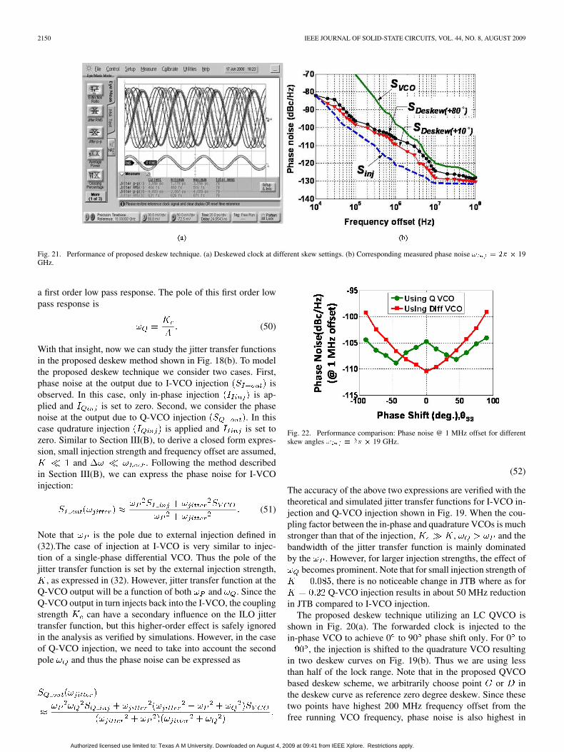
Fig. 21. Performance of proposed deskew technique. (a) Deskewed clock at different skew settings. (b) Corresponding measured phase noise � � �� � 19GHz.
a first order low pass response. The pole of this first order lowpass response is
(50)
With that insight, now we can study the jitter transfer functionsin the proposed deskew method shown in Fig. 18(b). To modelthe proposed deskew technique we consider two cases. First,phase noise at the output due to I-VCO injection isobserved. In this case, only in-phase injection is ap-plied and is set to zero. Second, we consider the phasenoise at the output due to Q-VCO injection . In thiscase qudrature injection is applied and is set tozero. Similar to Section III(B), to derive a closed form expres-sion, small injection strength and frequency offset are assumed,
and . Following the method describedin Section III(B), we can express the phase noise for I-VCOinjection:
(51)
Note that is the pole due to external injection defined in(32).The case of injection at I-VCO is very similar to injec-tion of a single-phase differential VCO. Thus the pole of thejitter transfer function is set by the external injection strength,
, as expressed in (32). However, jitter transfer function at theQ-VCO output will be a function of both and . Since theQ-VCO output in turn injects back into the I-VCO, the couplingstrength can have a secondary influence on the ILO jittertransfer function, but this higher-order effect is safely ignoredin the analysis as verified by simulations. However, in the caseof Q-VCO injection, we need to take into account the secondpole and thus the phase noise can be expressed as
Fig. 22. Performance comparison: Phase noise @ 1 MHz offset for differentskew angles � � �� � 19 GHz.
(52)
The accuracy of the above two expressions are verified with thetheoretical and simulated jitter transfer functions for I-VCO in-jection and Q-VCO injection shown in Fig. 19. When the cou-pling factor between the in-phase and quadrature VCOs is muchstronger than that of the injection, , and thebandwidth of the jitter transfer function is mainly dominatedby the . However, for larger injection strengths, the effect of
becomes prominent. Note that for small injection strength of, there is no noticeable change in JTB where as for
Q-VCO injection results in about 50 MHz reductionin JTB compared to I-VCO injection.
The proposed deskew technique utilizing an LC QVCO isshown in Fig. 20(a). The forwarded clock is injected to thein-phase VCO to achieve 0 to 90 phase shift only. For 0 to
, the injection is shifted to the quadrature VCO resultingin two deskew curves on Fig. 19(b). Thus we are using lessthan half of the lock range. Note that in the proposed QVCObased deskew scheme, we arbitrarily choose point or inthe deskew curve as reference zero degree deskew. Since thesetwo points have highest 200 MHz frequency offset from thefree running VCO frequency, phase noise is also highest in
Authorized licensed use limited to: Texas A M University. Downloaded on August 4, 2009 at 09:41 from IEEE Xplore. Restrictions apply.

HOSSAIN AND CARUSONE: CMOS OSCILLATORS FOR CLOCK DISTRIBUTION AND INJECTION-LOCKED DESKEW 2151
Fig. 23. Implementation of proposed deskew technique with a ring oscillator.
Fig. 24. (a) Generated skew curve as a function of free running frequency (� � �� � 10 GHz and � � ����). (b) Measured Phase noise for � � �� and� � �� .
these two points. On the other hand, point and is usedas and deskew respectively. Since the frequencyoffset is zero, lowest phase noise is achieved. Variation of thejitter tracking bandwidth with frequency offset (hence, deskew)is nonlinear (Fig. 15). For example, if K=0.17, a frequencyoffset of 150 MHz cause only 50 MHz reduction in JTB.It turns out that amplitude variation is also minimal in thatrange. Thus, the proposed technique allows us to accomplish
to phase selection with linear phase steps andnegligible amplitude variation, as shown in Fig. 21(a). Notethat point and on the deskew curve Fig. 20(b) represents0 and 90 phase shift. In the proposed technique, these twodeskew angles are obtained by setting same frequency offset
(200 MHz) and by switching the injection node from I-VCOto Q-VCO. As discussed earlier, switching the injection nodefrom I-VCO to Q-VCO has little effect on JTB if . Asa result only small variation of the phase noise of the deskewedclock in observed in Fig. 21(b). For comparison with a simpledifferential injection-locked VCO, the phase noise at 1 MHzoffset is plotted versus deskew angle in Fig. 22 which verifiesthe advantage of the proposed technique. In the worst casecondition ( or ) 8 dB of phase noise improvement isobtained. Note that in the plot of Fig. 21 the reference phaseangle of 0 is shifted by 45 in the Q-VCO case so that bothplots cover the same range.
Authorized licensed use limited to: Texas A M University. Downloaded on August 4, 2009 at 09:41 from IEEE Xplore. Restrictions apply.

2152 IEEE JOURNAL OF SOLID-STATE CIRCUITS, VOL. 44, NO. 8, AUGUST 2009
In a practical system, phase selection can be performed asin a conventional phase-locked or delay-locked loop. For ex-ample, in [26] the ILO output is compared to a reference clockby a phase detector which in turn drives a loop filter that tunesthe ILO. In a data recovery system, a data-driven phase detectorwould be required. Eventually the loop converges to a point ei-ther on the curve or . Note that these twocurves have overlap which may cause ambiguity in the controllogic. For example, 0 phase deskew can be achieved either bychoosing the point C or D. This problem can easily be solvedby adding hysteresis in the control logic.
B. Deskew With Ring Oscillator
If the link needs to support wide range of data rates, ringoscillators are often preferred over LC-VCOs due to theirwide tuning range. The proposed deskew technique is easilyrealizable for those applications. From Table III, increasingthe number of stages provides more nodes for injection thusthe opportunity to restrict over a narrower range providingmore linear phase adjustment. On the other hand, fewer stagesprovides lower power consumption and higher jitter trackingbandwidth. As a proof of concept, a four stage ring oscillatorimplemented in 90 nm CMOS is used in this study. The oscil-lator provides a tuning range from 2 GHz-7 GHz. The injectionsignal is at (Fig. 23). Similar to the LC oscillator, phasedeskew curves for both in-phase and quadrature injection areshown in Fig. 24. The effects of quadrature injection on jitterfiltering and amplitude variations are very similar to the LCoscillator case.
V. CONCLUSION
In summary, a low power clock source that incorporates abuffer into a cross-coupled oscillator has been demonstrated.By isolating the load from the tank, the oscillator can directlydrive 50-Ohm impedances or large capacitive loads with no ad-ditional buffering. A QVCO using this topology in 0.13 m dig-ital CMOS oscillates at 20 GHz, consumes 20 mW and provides12% tuning range with a measured phase noise is dBc Hz@ 1 MHz frequency offset. Injection-locked QVCOs are par-ticularly useful as deskew elements in high-speed parallel links.By selectively injecting different phases of a quadrature-LC orring VCO, variations in the ILO’s jitter tracking bandwidth aremuted and phase noise can be reduced. For a fixed data rate, LCoscillators can provide lower phase noise whereas ring oscilla-tors are preferred for variable data rates. Due to the additionalVCO stages in quadrature, this technique will consume morepower compared to [6] and [7]. The technique is demonstratedusing a LC QVCO at 20 GHz while burning only 20 mW ofpower and providing an 8 dB improvement in phase noise. Aring oscillator deskews a 2 to 7 GHz clock while consuming14 mW in 90 nm CMOS. These figures still compare favorablywith using a complete DLL for deskewing. In addition, ILOs aremore immune to supply noise and duty cycle distortion.
APPENDIX
In the case of a ring oscillator, the VCO transfer functionis low pass. Assume the ring oscillator is implemented with
identical stages. Each stage had a dc gain of and single pole. Thus the equivalent transfer function can be written as
(53)
Considering the positive feedback introduces 180 phaseshift, the remaining phase shift required to ensure oscillation at
is
(54)
(55)
Substituting (55) into (53)
(56)
(57)
Substituting this into (21) gives
(58)
Adopting the approximation in (26) gives
(59)
ACKNOWLEDGMENT
The authors would like to acknowledge F. O’Mahony,M. Mansuri, and B. Casper of the Intel Circuits Research Labat Hillsboro, Oregon, for their contribution to the clock deskewtechnique presented in this work.
REFERENCES
[1] H. Takauchi et al., “A CMOS multichannel 10-Gb/s transceiver,” IEEEJ. Solid-State Circuits, vol. 38, no. 12, pp. 2094–2100, Dec. 2003.
[2] B. Casper et al., “A 20 Gb/s forwarded clock transceiver in 90-nmCMOS,” in IEEE ISSCC Dig. Tech. Papers, 2006, pp. 90–91.
[3] F. O’mahony et al., “A low-jitter PLL and repeaterless network for a20 Gb/s link,” in IEEE Symp. VLSI Circuits Dig., 2006.
[4] R. Kreienkamp et al., “A 10-Gb/s CMOS clock and data recovery cir-cuit with an analog phase interpolator,” IEEE J. Solid-State Circuits,vol. 40, no. 3, pp. 736–743, Mar. 2005.
[5] C. Kromer et al., “A 25-Gb/s cdr in 90-nm CMOS for high-densityinterconnects,” IEEE J. Solid-State Circuits, vol. 41, no. 12, pp.2921–2929, Dec. 2006.
[6] L. Zhang, B. Ciftcioglu, M. Huang, and H. Wu, “Injection-lockedclocking: A new GHz clock distribution scheme,” presented at theIEEE Custom Integrated Circuits Conf., San Jose, CA, Sep. 2006.
[7] F. O’Mahony et al., “A 27 Gb/s forwarded clock I/O receiver usingan injection-locked LC-DCO in 45 nm CMOS,” in IEEE ISSCC Dig.,2008.
Authorized licensed use limited to: Texas A M University. Downloaded on August 4, 2009 at 09:41 from IEEE Xplore. Restrictions apply.

HOSSAIN AND CARUSONE: CMOS OSCILLATORS FOR CLOCK DISTRIBUTION AND INJECTION-LOCKED DESKEW 2153
[8] M. Tiebout, “Low power low-phase-noise differentially tuned quadra-ture VCO design in standard cmos,” IEEE J. Solid-State Circuits, vol.36, no. 5, pp. 1018–1024, May 2001.
[9] D. Ham and A. Hajimiri, “Concepts and methods in optimization ofintegrated LC VCOs,” IEEE J. Solid-State Circuits, vol. 36, no. 6, pp.896–909, Jun. 2001.
[10] K. Kwok and J. Long, “A 23-to-29 GHz transconductor-tuned VCOMMIC in 0.13 �m CMOS,” IEEE J. Solid-State Circuits, vol. 42, no.12, pp. 2878–3997, Dec. 2007.
[11] N. Nguyen and R. G. Meyer, “Start up and frequency stability in high-frequency oscillators,” IEEE J. Solid-State Circuits, vol. 27, no. 5, pp.810–820, May 1992.
[12] R. Aparicio and A. Hajimiri, “A noise-shifting differential ColpittsVCO,” IEEE J. Solid-State Circuits, vol. 37, no. 12, pp. 1728–1736,Dec. 2002.
[13] K. W. Tang et al., “Frequency scaling and topology comparison ofmm-wave CMOS VCOs,” in Proc. IEEE CSICS, Nov. 2006, pp. 55–58.
[14] A. Lacatia, S. Levantino, and C. Samori, Integrated Frequency Synthe-sizers for Wirelss Systems, 1st ed. Cambridge, UK: Cambridge Univ.Press, 2007, pp. 86–95.
[15] International Technology Roadmap of Semiconductors, ITRS, 2003[Online]. Available: www.itrs.org
[16] S. Li, I. Kipnis, and M. Ismail, “A 10-GHz CMOS quadrature LC-VCOfor multicore optical applications,” IEEE J. Solid-State Circuits, vol.38, no. 10, pp. 1626–1634, Oct. 2003.
[17] F. Ellinger and H. Jäckel, “38-43 ghz quadrature vco on 90 nm vlsicmos with feedback frequency tuning,” in IEEE MTT-S Int. MicrowaveSymp. Dig., 2005, p. 3.
[18] H. R. Rategh and T. H. Lee, “Superharmonic injection-locked fre-quency dividers,” IEEE J. Solid-State Circuits, vol. 34, no. 6, pp.813–821, Jun. 1999.
[19] H. Ng et al., “A second-order semidigital clock recovery circuit basedon injection locking,” IEEE J. Solid-State Circuits, vol. 38, no. 12, pp.2101–2110, Dec. 2003.
[20] R. Adler, “A study of locking phenomena in oscillators,” Proc. IRE,vol. 33, pp. 351–357, Jun. 1946.
[21] L. J. Paciore, “Injection locking of oscillators,” Proc. IEEE, vol. 53, no.11, pp. 1723–1728, Nov. 1965.
[22] M. Mansuri et al., “Strong injection locking of low-q lc oscillators,”presented at the IEEE Custom Integrated Circuits Conf., San Jose, CA,Sep. 2008.
[23] B. Razavi, “A study of injection locking and pulling in oscillators,”IEEE J. Solid-State Circuits, vol. 39, no. 9, pp. 1415–1424, Sep. 2004.
[24] X. Zhang, X. Zhou, B. Aliener, and A. S. Daryoush, “A study of subhar-monic injection locking for local oscillators,” IEEE Microwave GuidedWave Lett., vol. 2, pp. 97–99, Mar. 1992.
[25] A. Mirzaei, M. Heidari, R. Bagheri, S. Chehrazi, and A. Abidi, “Thequadrature LC oscillator: A complete portrait based on injectionlocking,” IEEE J. Solid-State Circuits, vol. 42, no. 9, pp. 1916–1932,Sep. 2007.
[26] J. Lee, H. Wang, W. Chen, and Y. Lee, “Subharmonically injection-locked plls for ultra-low-noise clock generation,” in IEEE ISSCC Dig.,2009.
Masum Hossain received the B.Sc. degree inelectrical engineering from Bangladesh Universityof Engineering and Technology, Bangladesh, and theM.Sc. degree from Queen’s University, Canada, in2002 and 2005, respectively. During his M.Sc., heworked on K-band wireless receiver in CMOS. Since2005, he has been working towards the Ph.D. degreein electrical engineering at University of Toronto.
From September 2007 to January 2008, he waswith Intel Circuit Research Lab (CRL) as a graduateintern. Currently, he is working for Gennum Corp.
in the Analog and Mixed Signal division. His research interests include mixedsignal circuits for high-speed chip-to-chip communications, low power VCO,phase interpolator and clock recovery techniques. He won the Best StudentPaper Award at the 2008 Custom Integrated Circuits (CICC) conference.
Anthony Chan Carusone (S’96–M’02–SM’08)received the B.A.Sc. and Ph.D. degrees from theUniversity of Toronto in 1997 and 2002, respectively,during which time he received the Governor-Gen-eral’s Silver Medal.
Since 2001, he has been with the Department ofElectrical and Computer Engineering at the Univer-sity of Toronto where he is currently an AssociateProfessor. In 2008 he was a visiting researcher at theUniversity of Pavia, Italy, and later at the Circuits Re-search Lab of Intel Corp., Hillsboro, Oregon.
Prof. Chan Carusone was a co-author of the best paper at the 2005 Com-pound Semiconductor Integrated Circuits Symposium and the best student pa-pers at both the 2007 and 2008 Custom Integrated Circuits Conferences. He isan appointed member of the Administrative Committee of the IEEE Solid-StateCircuits Society, a member and past chair of the Analog Signal Processing Tech-nical Committee for the IEEE Circuits and Systems Society, and a memberand past chair of the Wireline Communications subcommittee of the CustomIntegrated Circuits Conference. He serves as a guest editor for both the IEEEJOURNAL OF SOLID-STATE CIRCUITS and the IEEE TRANSACTIONS ON CIRCUITS
AND SYSTEMS I: REGULAR PAPERS. He is currently Editor-in-Chief of the IEEETRANSACTIONS ON CIRCUITS AND SYSTEMS II: EXPRESS BRIEFS.
Authorized licensed use limited to: Texas A M University. Downloaded on August 4, 2009 at 09:41 from IEEE Xplore. Restrictions apply.
Related Documents