Energy Sciences Strategic Plan 2016

Welcome message from author
This document is posted to help you gain knowledge. Please leave a comment to let me know what you think about it! Share it to your friends and learn new things together.
Transcript

Energy SciencesStrategic Plan
2016

Cover background image: An international team of researchers including MSD and Molecular Foundry staff has produced 3D Structure Identification of Nanoparticles by Graphene Liquid Cell Electron Microscopy (SINGLE), a capability that was used to separately reconstruct the 3D structures of two individual platinum nanoparticles in solution in a graphene liquid cell. Park, et al. Science 2015 doi:10.1126/science.aab1343.
From left to right: Senior Scientist Jinghua Guo of the Advanced Light Source performs in situ X-ray absorption spectroscopy on materials for artificial photosynthesis and energy storage at beamline 6.3.1.2.
Jim Schuck, Imaging and Manipulation of Nanostructures Facility Director at the Molecular Foundry, uses optical techniques to understand the fundamental properties of materials on the nanoscale.
Summer intern Rupika Malik works with mentor Daniel Slaughter of the Atomic, Molecular, and Optical Sciences group in the Chemical Sciences Division.

Energy SciencesStrategic Plan
2016

| 2
MSD staff scientist Haimei Zheng uses the TitanX electron microscope at the National Center for Electron Microscopy facility of the Molecular Foundry for research in platinum-colbalt nanocatalysts.

ENERGY SCIENCES | TABLE OF CONTENTS
| 3
Executive Summary 4
Introduction 9
ENERGY SCIENCES AREA OVERVIEW 10
Core Scientific Disciplines 12
MATERIALS SCIENCES 13
CHEMICAL SCIENCES 20
Transformative Research Facilities 28
ADVANCED LIGHT SOURCE 29
THE MOLECULAR FOUNDRY 38
Crosscutting Research Opportunities and Strategies 48
ENERGY INNOVATION HUBS 49
ENERGY FRONTIER RESEARCH CENTERS 52
THE MATERIALS PROJECT 53
CENTER FOR ADVANCED MATHEMATICS FOR ENERGY RESEARCH APPLICATIONS (CAMERA) 55
Emerging Opportunities 57
LEVERAGING SOFT X-RAY PHASE COHERENCE: ALS-U 58
FUTURE DIRECTIONS IN ELECTRON MICROSCOPY 59
ENERGY SCIENCES CAMPUS 61
INDUSTRY CONNECTIONS 63
Table of Contents

At Lawrence Berkeley National Laboratory (Berkeley Lab), a U.S.
Department of Energy (DOE) laboratory, researchers under the
administrative umbrella of the Energy Sciences Area are seeking
technological solutions to major energy-related challenges that impact
not only the global economy but also our planet itself. In keeping with
the “team science” concept that is the hallmark of Berkeley Lab, this
research is carried out across multiple scientific disciplines using the
most advanced tools and instrumentation available. Berkeley Lab’s
Energy Sciences Area encompasses the Materials Sciences Division, the Chemical Sciences Division, and two DOE Office of Science national
scientific user facilities — the Advanced Light Source and the
Molecular Foundry — plus several crosscutting research centers and
facilities. The Energy Sciences Strategic Plan presented here describes
a 10-year roadmap for scientific studies that will advance the cause of a
sustainable energy future.
Executive Summary

ENERGY SCIENCES | EXECUTIVE SUMMARY
| 5
Widely recognized as a unique source of energy solutions, Berkeley Lab is home to a vibrant, interacting community of scientists with a collective fundamental understanding of today’s most pressing issues in energy science and technology. At Berkeley Lab, we seek to foster an environment in which disciplinary boundaries and loyalties are secondary to achieving critical scientific and technical objectives. We strive to maintain our position as a preferred source of scientific knowledge and information for public, industrial, and government constituencies. In this strategic plan, we describe our existing key strengths in each major disciplinary field within the Energy Sciences Area as well as new research opportunities that will build upon these strengths for new programmatic growth.
Examples of such opportunities are found in Berkeley Lab’s Materials Sciences Division, where researchers are focusing on the physics and chemistry of materials that harness quantum phenomena and nanoscale confinement, and materials properties and behavior that occur far from equilibrium, or are impacted by interfacing different materials or phases. Future energy materials, including atomically thin 2D materials, which form in crystalline sheets only a single atom in thickness, also hold great promise for future energy systems, including energy-efficient electronics and novel light-harvesting materials as well as quantum computing applications. To study and advance the development of novel materials, the Materials Sciences Division supports collaborative programs in both theory and experiment. Studies are being carried out in complex materials, correlated electron and spin systems, nanostructures, and catalytic systems. These studies are able to capitalize on advanced computational facilities, instrumentation, and cutting-edge synthesis and characterization techniques, such as ultrafast spectroscopy, diffraction, and microscopy.
A major focus of Berkeley Lab’s Chemical Sciences Division is to bridge the current gap between predictive science and complexity. Our ability to predict the outcome of chemical reactions today is based on models of simple systems isolated from the environment. Extending the predictive capabilities of our models to levels of complexity that more accurately model the behavior of systems in the real world would better enable scientists to address a number of critical energy-related issues including solar fuels, energy storage and batteries, gas-to-liquid fuels, industrial chemical processing of high-value chemicals, and the synthesis of functional materials for energy use. The Chemical Sciences Division maintains a research portfolio spanning a wide range of time and length scales in the atomic, molecular, and optical sciences; gas-phase and condensed-phase chemical physics; heavy element chemistry; and homogeneous and heterogeneous catalysis.
Berkeley Lab’s Advanced Light Source Division maintains and operates the Advanced Light Source (ALS), a synchrotron-based source of hard and soft X-ray, ultraviolet, and infrared light that is used to study the atomic and electronic structure of matter, specializing in surfaces and interfaces where most chemical activity takes place. The ALS is a DOE Office of Science national scientific user facility that offers a world-class suite of multiscale, multimodal imaging tools to probe the hierarchical structures of functional materials — biological as well as nonbiological — with high spatial, temporal, and spectral resolution. Featuring 40 beamlines that support the research of more than 2,000 users each year, the ALS and its experimental capabilities are being used to address key areas in the energy sciences, such as mapping electronic, ionic, and chemical pathways in catalysis, energy conversion, and energy storage; developing new functional materials for ultralow-power electronics; and illuminating the crossover between chemical dynamics and kinetics at the nanoscale.
The Molecular Foundry, a nanoscale science research center and DOE Office of Science national scientific user facility, provides users from around the world with access to cutting-edge expertise and instrumentation in a collaborative, multidisciplinary environment. The Molecular Foundry houses facilities that specialize in the imaging and manipulation of nanostructures, nanofabrication, the theory of nanostructured materials, inorganic nanostructures and biological nanostructures, and organic and macromolecular synthesis. It also hosts the National Center for Electron Microscopy (NCEM), home to TEAM 0.5 and TEAM 1, some of the world’s most powerful transmission electron microscopes (TEM). Researchers and facilities at the Molecular Foundry focus on program areas in combinatorial nanoscience for the

| 6
rational design of targeted nanostructured materials; functional nanointerfaces to better understand the physical and chemical properties of hybrid nanomaterials that contain both inorganic and organic components; multimodal imaging to investigate structural and dynamic phenomena in hard and soft nanostructured materials in a wide variety of environments; and nanofabrication and assembly for the structural organization of components with single-digit nanometer- and atomic-scale dimensions.
That these existing strengths within the Energy Sciences Area are being effectively used for pioneering scientific discoveries can be seen in a sample of recent scientific highlights:
• A potentially game-changing breakthrough in artificial photosynthesis with the development of a system that can capture carbon dioxide emissions before they are vented into the atmosphere and then, powered by solar energy, convert that carbon dioxide into valuable chemical products, including biodegradable plastics, pharmaceutical drugs, and even liquid fuels
• The development of sponge-like crystals of covalent organic frameworks (COFs) that not only absorb carbon dioxide, but also selectively reduce it to carbon monoxide, which serves as a primary building block for a wide range of chemical products, including fuels, pharmaceuticals, and plastics
• The discovery of a design rule for controlling the structure of 2D peptoid nanosheets so that they mimic the complexity and function of nature's proteins while retaining the durability of synthetic materials
• The combination of designer quantum dot light emitters with spectrally matched photonic mirrors to create solar cells that collect blue photons at 30 times the concentration of conventional solar cells, the highest luminescent concentration factor ever recorded
• The development of a technique for effectively controlling pulses of light in closely packed nanoscale waveguides, an essential requirement for high-performance optical communications and chip-scale quantum computing.
• The synthesis of a new “high-entropy alloy” that not only tests out as one of the toughest materials on record but also exhibits improved toughness, strength, and ductility at cryogenic temperatures
• The creation of a new technique for predicting the nonlinear optical properties of metamaterials, artificial nanostructures engineered with electromagnetic properties not found in nature
• The discovery that properly managed exposure to alpha-particle radiation can greatly enhance the performance of certain thermoelectrics — materials that can convert heat into electricity, or electricity into cooling
While these and the many other research achievements in the Energy Sciences Area are advancing specific programmatic goals as planned, we recognize that sometimes the most impactful discoveries are entirely unplanned, and that some of the biggest technology breakthroughs have come as a result of experiments undertaken with very different purposes in mind. Therefore, the vision of this strategic plan is to be sufficiently broad so as to align with the Grand Challenges of basic energy science established by the DOE Office of Science, our primary sponsor through its Office of Basic Energy Sciences. These Grand Challenges serve as a call-to-action for research aimed at helping to meet humanity’s most pressing needs, including the need for renewable, clean, and affordable energy sources that will spur economic prosperity while at the same time mitigating global climate change. By tackling the limitations of our understanding and theoretical capacity to model and predict physical and chemical phenomena at the molecular, atomic, and quantum levels, the proposals put forth in this strategic plan for Berkeley Lab’s Energy Sciences Area can help pave the way for transformative new technologies that generate, deliver, store, and conserve energy in ways we may not yet even imagine.
ENERGY SCIENCES | EXECUTIVE SUMMARY
| 7
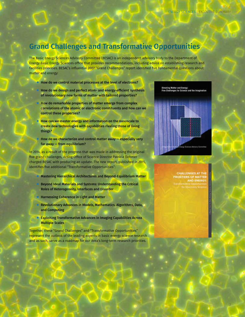
Grand Challenges and Transformative OpportunitiesThe Basic Energy Sciences Advisory Committee (BESAC) is an independent advisory body to the Department of Energy Basic Energy Sciences office that provides recommendations, including advice on establishing research and facilities priorities. BESAC’s influential 2007 “Grand Challenges” report identified five fundamental questions about matter and energy:
• How do we control material processes at the level of electrons?
• How do we design and perfect atom- and energy-efficient synthesis of revolutionary new forms of matter with tailored properties?
• How do remarkable properties of matter emerge from complex correlations of the atomic or electronic constituents and how can we control these properties?
• How can we master energy and information on the nanoscale to create new technologies with capabilities rivaling those of living things?
• How do we characterize and control matter away — especially very far away — from equilibrium?
In 2014, as a result of the progress that was made in addressing the original five grand challenges, Acting Office of Science Director Patricia Dehmer charged BESAC with producing an update. The new report, published in 2015, identifies five additional “Transformative Opportunities”:
• Mastering Hierarchical Architectures and Beyond-Equilibrium Matter
• Beyond Ideal Materials and Systems: Understanding the Critical Roles of Heterogeneity, Interfaces and Disorder
• Harnessing Coherence in Light and Matter
• Revolutionary Advances in Models, Mathematics, Algorithms, Data, and Computing
• Exploiting Transformative Advances in Imaging Capabilities Across Multiple Scales
Together, these “Grand Challenges” and “Transformative Opportunities” represent the outlook of the leading experts in basic energy science research and as such, serve as a roadmap for our Area’s long-term research priorities.

Vision Statement
The Energy Sciences Area fosters an environment that promotes
integrated fundamental research and provides unique tools
to achieve transformational breakthroughs in energy science.
Purpose of the Plan
• Identify crosscutting goals and strategies that define and unite Energy Sciences
• Identify new knowledge areas and research opportunities needed to further advance Energy Sciences
• Provide a roadmap for future decision making, including funding sources and opportunities
Time Frame
• Ten years, with nearer-term goals and milestones in the three-to five-year range
Berkeley Lab Values
• Overarching commitment to pioneering science
• Highest integrity/impeccable ethics
• Uncompromising safety
• Diversity in people and thought
• Sense of urgency

ENERGY SCIENCES | INTRODUCTION
| 9
Berkeley Lab’s defining features are the creation of interdisciplinary
teams that dissolve ordinary institutional boundaries to tackle new
frontiers in science, and world-leading facilities, instruments, and
computational capabilities. The people and facilities of Berkeley Lab’s
Energy Sciences Area are the most distinguished, productive, and
impactful in the Department of Energy (DOE) complex of 17 national
laboratories. With a long and rich history extending to the earliest
days of the nation’s first national laboratory, the Energy Sciences
Area remains at the forefront of discovery science, as evidenced by its
preeminent record of high-impact research publications, prestigious
awards, patents, and licensed technologies.
While we know we can’t predict the exciting and often unexpected future of basic science, we must lay the groundwork for continued leadership well into the 21st century with advanced facilities and instrumentation. Berkeley Lab's pioneering "team science" approach to the largest and most important scientific problems will continue to provide the discoveries that have solidified our reputation as a leading basic science national laboratory.
Berkeley Lab is a scientifically diverse organization, with research divisions covering energy-related topics, including materials sciences, climate modeling, building technologies, biophysics, energy-efficiency policy, geology, ecosystems dynamics, chemistry, and biofuels. The domed roof that once housed Ernest Orlando Lawrence’s 184-inch Cyclotron now sits atop one of the world’s brightest soft X-ray and ultraviolet synchrotron light sources, the Advanced Light Source (ALS), a national scientific user facility that is accessible to researchers from around the world. At the Molecular Foundry, another national scientific user facility located just down the road from the ALS, a multidisciplinary team of researchers focuses on all things nano — from combinatorial nanoscience to nanointerfaces, nanoimaging, nanofabrication, and a full suite of world-class electron microscopes and experts.
Today, as our predecessors did in 1939, we find ourselves facing a pressing global challenge. The link between the world’s energy needs and the global carbon cycle, combined with a large, growing, and energy-hungry world population, is a daunting but inescapable and mounting problem.
Introduction
ENERGY SCIENCES | INTRODUCTION
| 10
Energy Sciences Area Overview
The Energy Sciences Area at Berkeley Lab is comprised of three
divisions that receive the bulk of Berkeley Lab’s funding from the Office
of Basic Energy Sciences (BES). BES is the largest office within the
Department of Energy’s Office of Science.
Materials Sciences DivisionThe Materials Sciences Division (MSD) has over 100 principal investigators, 60 with joint university faculty positions, about 100 technical and administrative staff, and about 500–600 affiliates. It has an annual budget of $75 million, and over 600 annual publications. MSD’s core programs receive funding from three research areas within the BES Materials Sciences and Engineering Division: Materials Discovery, Design, and Synthesis; Condensed Matter and Materials Physics; and Scattering and Instrumentation Sciences. The core programs at MSD target a large variety of materials chemistry, materials physics, and instrumentation aspects, such as quantum materials, non-equilibrium magnetic materials, electronic materials, metamaterials, sp2-bonded materials, chemical and mechanical properties of surfaces, interfaces and nanostructures, physical chemistry of inorganic nanostructures, inorganic/organic nanocomposites, soft matter, functional nanomachines, mechanical behavior and ultrafast behavior of materials, nuclear magnetic resonance, as well as substantial theoretical and computational efforts for materials sciences, including the Materials Project. MSD is also home of the Center for X-ray Optics (CXRO), a unique, world-renowned facility working to further the science and technology of short wavelength optical systems and technique. CXRO’s research activities are primarily funded by semiconductor industries, but it also operates several beamlines at the ALS.
Chemical Sciences DivisionThe Chemical Sciences Division has approximately 275 employees and affiliates and an annual budget of $25 million. The division is organized into five core programs: Atomic, Molecular, and Optical Sciences; Catalysis and Chemical Transformations; Condensed Phase and Interfacial Molecular Science (CPIMS); Gas Phase Chemical Physics; and Heavy Element Chemistry. In addition, four centers and facilities provide unique capabilities to carry out cutting-edge research in the division: the Joint Center for Artificial Photosynthesis (JCAP), a DOE Energy Innovation Hub; the Molecular Environmental Sciences (MES) Beamline and the Chemical Dynamics Beamline (CDB) at the ALS; the Heavy Element Research Laboratory (HERL); and the Ultrafast X-ray Science Laboratory (UXSL).
Erin Creel, a graduate student in JCAP's Photocatalysis and Light Capture thrust, injects gold nanosphere seeds into a metal precursor solution to make gold-titania core-shell nanoparticles.
ENERGY SCIENCES | ENERGY SCIENCES AREA OVERVIEW
| 11
Advanced Light SourceThe Advanced Light Source (ALS) is a third-generation synchrotron national scientific user facility that attracts scientists from around the world. It has an annual operating budget of approximately $60 million, a staff of 200, and over 900 refereed publications per year. The ALS hosts over 2,400 users per year who utilize the 40 beamlines to conduct research in energy science, geoscience, ecology, applied science, chemical science, life science, physics, and materials science. ALS staff includes beamline scientists, user program support staff, and the engineering personnel needed to operate the accelerator. The ALS is situated beneath an iconic dome, part of the original 1942 building designed by Arthur Brown, Jr. (the designer of numerous landmark buildings, including San Francisco’s Coit Tower) to house Ernest O. Lawrence’s 184-inch Cyclotron.
Molecular Foundry The Molecular Foundry is a BES-funded Nanoscale Science Research Center (NSRC), one of five NSRCs sponsored by BES at national labs across the country. The Molecular Foundry provides communities of users with capabilities to understand and control matter at the nanoscale in a multidisciplinary, collaborative environment. The Molecular Foundry hosts some 677 users each year with an annual budget of over $25 million, and is organized into seven facilities: Imaging and Manipulation of Nanostructures; Nanofabrication; Theory of Nanostructured Materials; Inorganic Nanostructures; Biological Nanostructures; Organic and Macromolecular Synthesis; and the National Center for Electron Microscopy.
Other DOE Office of Basic Energy Sciences–funded Programs at Berkeley LabThe Department of Energy’s Office of Basic Energy Sciences (BES) funds a number of research programs at Berkeley Lab outside the three divisions that constitute the Energy Sciences Area. In the new Earth and Environmental Sciences Area, a strong and growing geosciences program thrives. BES investigators in the Molecular Biophysics & Integrated Bioimaging Division in the Biosciences Area study the mechanistic underpinnings of photosynthesis, both natural and bio-inspired. Major BES-funded research programs housed outside the Energy Sciences Area at Berkeley Lab include the Joint Center for Energy Storage Research (JCESR), led by the Energy Technologies Area), the Center for Advanced Mathematics for Energy Research Applications (CAMERA, led by the Computational Research Division), and the Center for Nanoscale Controls on Geologic CO2 (an Energy Frontier Research Center led by the Earth and Environmental Sciences Area).

| 12
Core Scientific Disciplines
Our research programs aim to discover, design, and understand new
materials and chemical transformations. The sustainable energy solutions
and technologies of the future require a steady supply of basic science
discoveries cultivated from a suite of scientific disciplines, including
condensed matter and materials physics, chemistry, geosciences, and
physical biosciences. This new knowledge base will form the foundation
for the energy systems of the future — from generating fuels from
sunlight, carbon dioxide, and water, to developing new ways of storing
power, or converting sunlight to electricity.
In the following sections, we describe the key opportunities and core
capabilities that combine to create Berkeley Lab’s unique and vibrant
vision for basic energy research.

ENERGY SCIENCES | CORE SCIENTIFIC DICIPLINES
| 13
Materials Sciences
IntroductionOur fundamental materials research is organized into three interconnected thematic areas, which enable the discovery and development of novel materials systems:
Novel quantum materials, which consist of novel phases that occur due to quantum effects on the nanoscale and give rise to materials with unprecedented properties and behavior
Dynamical processes in materials — the excitation of materials into highly perturbed excited states will help us to understand the behavior and properties of new materials and thus the design of novel matter
Understanding and tailoring the interfaces between two different phases — e.g., solid-solid, solid-liquid, solid-gas, liquid-liquid, or liquid-gas
At Berkeley Lab’s Materials Sciences Division, we advance the fundamental science of materials within the context of global energy-related challenges. We develop and apply experimental and theoretical techniques to design, discover, and understand new materials and phenomena at multiple time, length, and energy scales. Through our core programs, user facilities, and research centers, we cultivate a collaborative and interdisciplinary approach to materials research and help train the next generation of materials scientists.
MSD’s research activities follow a three-pronged approach — encompassing materials chemistry, materials physics, and instrumentation sciences — to address challenges in the three interconnected themes of materials in the quantum regime, materials interfaces, and materials dynamics (Figure 1).
As part of its vision for the future, MSD’s strategy focuses on research at the frontiers of our understanding of matter, including to:
• Understand, manipulate, and control competing forms of order that arise through interactions shaped by quantum physics, e.g., atomically thin 2D materials; the ultrafast dynamics of materials, which are excited into far-from-equilibrium states; and to
• Study the physical and chemical processes in materials under environmental conditions, e.g., chemical transformations with atomic resolution
Figure 1: Three interconnected themes govern MSD’s research activities.
Interfacessolid|liquid|gas
inorganic|organic
Dynamicsas|fs|ps|ns
transformations
Quantum Matternano|meso
correlated materialsmetamaterials
Interfacessolid|liquid|gas
inorganic|organic
Dynamicsas|fs|ps|ns
transformations
Quantum Matternano|meso
correlated materialsmetamaterials

| 14
These research thrust areas are consistent with the goals of BES, which advances the aim “to understand, predict, and ultimately control matter and energy at the electronic, atomic, and molecular levels in order to provide the foundations for new energy technologies.”
The following Key Strengths section describes MSD’s current core program research, and the New Research Opportunities section describes our future vision. The broad research activities within the Materials Project are described in Section 5, Crosscutting Research Opportunities and Strategies.
Key Strengths
Synthesis and Characterization of Nanomaterials
Theory and experiment are both essential to understand how new materials function. This program area supports fundamental research on the development of innovative synthesis and processing methods.
MSD’s atomic-level studies of surfaces and nanomaterials focusing on such properties as structure, diffusion, reactions, catalysis, friction, and wear generate knowledge that will speed the development of novel catalysts with higher activity and selectivity.
Current research will continue in the pursuit of synthetically controlling nanocrystals and nanowires for use in integrated systems, and the establishment of core science and technology to produce, separate, and transport charges. This research will emphasize the synthesis and integration of inorganic nanomaterials, and the characterization of their physical properties using, for example, X-ray transient absorption spectroscopy and single-particle fluorescence.
Assemblies of nanoparticles and organic building blocks hold promise for generating composites with special properties. MSD’s long-term goal is to generate structured nanocomposites with tunable optical, electronic, and mechanical properties for energy applications. The resultant structured functional nanocomposites will provide a robust platform to investigate mesoscale phenomena and functionality.
Materials science research will work toward developing, characterizing, and better understanding the fundamental behavior of mechanical structures at the nanoscale. The two paths toward this goal include designing new synthetic molecular machines in a molecule-by-molecule fashion. Additionally, work is performed on the design, synthesis, characterization, and application of “sp2-bonded materials” whose dimensions range from 1–100 nm, with a focus on the prediction and examination of new stable structures, methodologies to integrate distinct nanostructures, and novel synthesis methods for non-equilibrium growth of sp2-based materials. The sp2-bonded materials include carbon-based structures, such as nanotubes, graphene, and nanowires, as well as non-carbon-based materials, such as boron nitride.
Novel Materials and Assemblies
MSD’s portfolio of ongoing programs will continue its focus on the design and discovery of novel materials and material constructs. One aspect is to design, synthesize, and characterize (structurally and mechanically) a new series of hybrid structural materials whose unique properties are derived from hierarchical architectures controlled over length scales ranging from the nano- to macroscale dimension. The goal is to defeat the law of mixtures (as found in nature) by devising complex hierarchical structures comprised of weak constituents into strong and tough hybrid (polymer-ceramic and metal-ceramic) materials that display far superior properties than their individual constituents.
Quantum Matter and Interfaces
A strong focus is on condensed matter systems in which quantum mechanics plays an especially important role in determining the nature of ordered phases and the transitions that take place between them. This research currently includes transition metal oxides, such as cuprate and iron-pnictide superconductors, and iridates that exhibit novel forms of magnetic and topological order.
ENERGY SCIENCES | CORE SCIENTIFIC DICIPLINES
| 15
Harnessing competing interactions — such as spin-orbit coupling at interfaces leading to noncollinear spin textures — enables the design, discovery, and understanding of the static and dynamic properties of novel magnetic ground states that provide insight into fundamental properties of magnetic materials, but could also open the path to novel energy-efficient magnetic materials for future information technologies.
The performance and reliability of semiconductor technologies, including solar power conversion devices, solid state sources of visible light, visual displays, and a large variety of sensors and power control systems, will be improved by expanding the fundamental understanding of the relationships between synthesis and processing conditions, and the structure, properties, and stability of semiconductor materials systems.
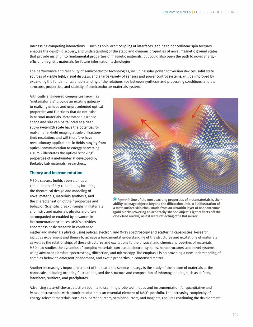
Artificially engineered composites known as “metamaterials” provide an exciting gateway to realizing unique and unprecedented optical properties and functions that do not exist in natural materials. Metamaterials whose shape and size can be tailored at a deep sub-wavelength scale have the potential for real-time far-field imaging at sub-diffraction-limit resolution, and will therefore have revolutionary applications in fields ranging from optical communication to energy harvesting. Figure 2 illustrates the optical “cloaking” properties of a metamaterial developed by Berkeley Lab materials researchers.
Theory and Instrumentation
MSD’s success builds upon a unique combination of key capabilities, including the theoretical design and modeling of novel materials, materials synthesis, and the characterization of their properties and behavior. Scientific breakthroughs in materials chemistry and materials physics are often accompanied or enabled by advances in instrumentation sciences. MSD’s activities encompass basic research in condensed matter and materials physics using optical, electron, and X-ray spectroscopy and scattering capabilities. Research includes experiment and theory to achieve a fundamental understanding of the structures and excitations of materials as well as the relationships of these structures and excitations to the physical and chemical properties of materials. MSD also studies the dynamics of complex materials, correlated electron systems, nanostructures, and novel systems using advanced ultrafast spectroscopy, diffraction, and microscopy. The emphasis is on providing a new understanding of complex behavior, emergent phenomena, and exotic properties in condensed matter.
Another increasingly important aspect of the materials science strategy is the study of the nature of materials at the nanoscale, including ordering fluctuations, and the structure and composition of inhomogeneities, such as defects, interfaces, surfaces, and precipitates.
Advancing state-of-the-art electron beam and scanning probe techniques and instrumentation for quantitative and in situ microscopies with atomic resolution is an essential element of MSD’s portfolio. The increasing complexity of energy-relevant materials, such as superconductors, semiconductors, and magnets, requires continuing the development
Figure 2: One of the most exciting properties of metamaterials is their ability to image objects beyond the diffraction limit. A 3D illustration of a metasurface skin cloak made from an ultrathin layer of nanoantennas (gold blocks) covering an arbitrarily shaped object. Light reflects off the cloak (red arrows) as if it were reflecting off a flat mirror.

| 16
TEN-YEAR GOALS, MILESTONES, AND ACHIEVEMENTS THAT CONSTITUTE SUCCESS:
Study the coupling of charge, spin, and valley degree of freedom
Investigate ordering, dynamics, and unusual excitations
Discover new topologies at protected surface states that are relevant to electrocatalytic processes
Explore coherence and correlations leading to long-lived quantum coherence
and improvement of next-generation optical, electron, X-ray, neutron scattering, and nuclear magnetic resonance (NMR) instrumentation for characterizing the atomic, electronic, and magnetic structures of materials. This objective includes a full range of elastic, inelastic, and imaging techniques as well as ancillary technologies, such as novel detectors, sample environments, and data analysis.
MSD and its researchers continue to develop unique capabilities, including the development of new tools for in situ characterization of solid-gas interfaces at ambient pressure, and of solid-liquid interfaces, mostly with scanning tunneling microscopy (STM) and ambient pressure photoelectron spectroscopy (APPES). These have opened completely new possibilities to study the physics and chemistry of surfaces with materials under ambient conditions, which are highly relevant in such applications as catalysis and batteries. It is worth noting that instruments developed by MSD researchers have had a significant impact in other facilities worldwide.
Future theory and instrumentation research also includes the development of predictive models for the discovery of new materials with targeted properties, identifying the properties of new materials, and the interpretation of experiments (see Figure 3). The new models will emphasize co-operative and correlation effects that can lead to the formation of new quasi-particles, new phases of matter, and unexpected phenomena.
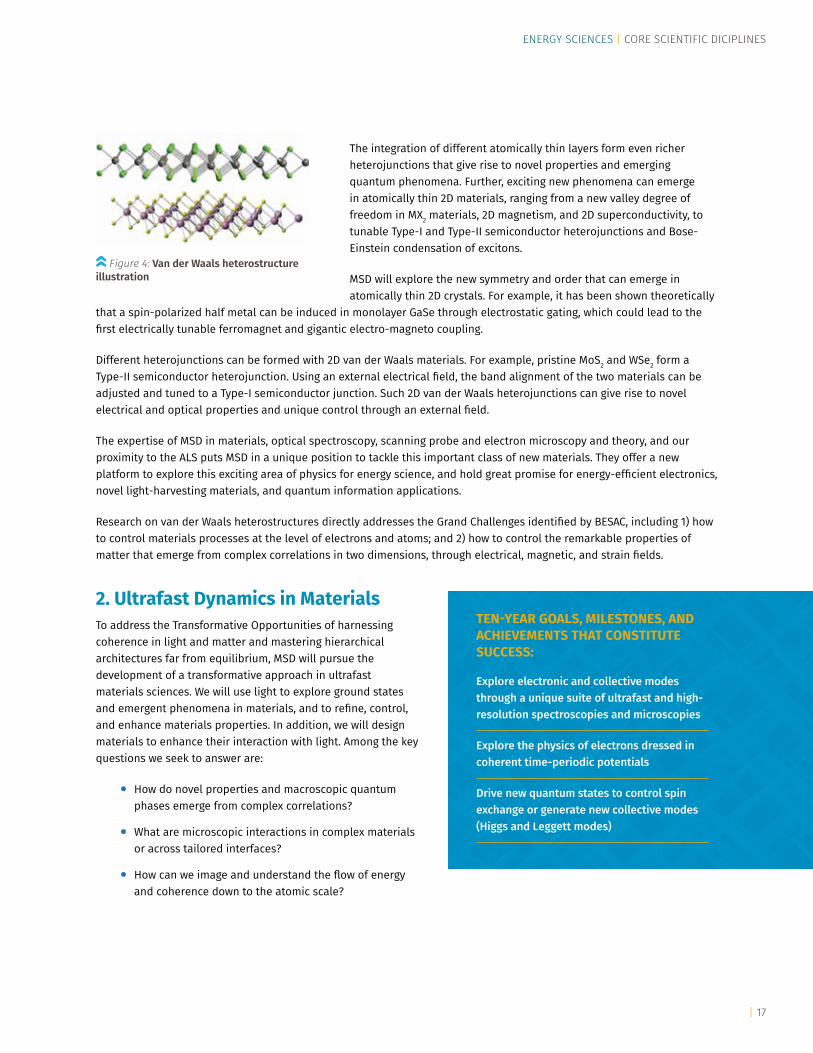
New Research Opportunities1. Novel Quantum Materials Condensed matter systems in which quantum mechanics play an especially important role offer a rich scientific area for determining the nature of ordered phases and the transitions that take place between them. In these systems, competing spin, orbital, and lattice interactions yield a multiplicity of nearly degenerate ground states and complex phase diagrams that can be challenging to characterize. Examples of emerging correlated quantum matter can be seen in multiferroics, superconducting and topological phases, and more recently in 2D systems, such as graphene or transition metal dichalcogenides. Two-dimensional heterostructures based on conventional III-V semiconductors have enabled emerging phenomena, from quantum Hall effects to Wigner crystals. They have revolutionized modern electronics and photonics, ranging from semiconductor LEDs (which won a Nobel Prize in 2014) and lasers to high-speed transistors. However, conventional semiconductor structures can be realized only in a few materials due to the requirements of lattice matching. The discovery of atomically thin 2D materials enables a rich variety of new van der
Waals heterostructures, in which different 2D crystals are stacked together (Figure 4). As the individual layers can be semiconductors, insulators, metals, or superconductors, these new van der Waals heterostructures offer tremendous new opportunities and flexibility to design and discover novel materials with unprecedented properties and functionalities.
Figure 3: Real-space exciton wavefunctions in monolayer WS2 can be determined from ab initio calculations, shedding light on the excitonic states of this TMDC material.
ENERGY SCIENCES | CORE SCIENTIFIC DICIPLINES
| 17
The integration of different atomically thin layers form even richer heterojunctions that give rise to novel properties and emerging quantum phenomena. Further, exciting new phenomena can emerge in atomically thin 2D materials, ranging from a new valley degree of freedom in MX2 materials, 2D magnetism, and 2D superconductivity, to tunable Type-I and Type-II semiconductor heterojunctions and Bose-Einstein condensation of excitons.
MSD will explore the new symmetry and order that can emerge in atomically thin 2D crystals. For example, it has been shown theoretically
that a spin-polarized half metal can be induced in monolayer GaSe through electrostatic gating, which could lead to the first electrically tunable ferromagnet and gigantic electro-magneto coupling.
Different heterojunctions can be formed with 2D van der Waals materials. For example, pristine MoS2 and WSe2 form a Type-II semiconductor heterojunction. Using an external electrical field, the band alignment of the two materials can be adjusted and tuned to a Type-I semiconductor junction. Such 2D van der Waals heterojunctions can give rise to novel electrical and optical properties and unique control through an external field.
The expertise of MSD in materials, optical spectroscopy, scanning probe and electron microscopy and theory, and our proximity to the ALS puts MSD in a unique position to tackle this important class of new materials. They offer a new platform to explore this exciting area of physics for energy science, and hold great promise for energy-efficient electronics, novel light-harvesting materials, and quantum information applications.
Research on van der Waals heterostructures directly addresses the Grand Challenges identified by BESAC, including 1) how to control materials processes at the level of electrons and atoms; and 2) how to control the remarkable properties of matter that emerge from complex correlations in two dimensions, through electrical, magnetic, and strain fields.
2. Ultrafast Dynamics in MaterialsTo address the Transformative Opportunities of harnessing coherence in light and matter and mastering hierarchical architectures far from equilibrium, MSD will pursue the development of a transformative approach in ultrafast materials sciences. We will use light to explore ground states and emergent phenomena in materials, and to refine, control, and enhance materials properties. In addition, we will design materials to enhance their interaction with light. Among the key questions we seek to answer are:
• How do novel properties and macroscopic quantum phases emerge from complex correlations?
• What are microscopic interactions in complex materials or across tailored interfaces?
• How can we image and understand the flow of energy and coherence down to the atomic scale?
Figure 4: Van der Waals heterostructure illustration
TEN-YEAR GOALS, MILESTONES, AND ACHIEVEMENTS THAT CONSTITUTE SUCCESS:
Explore electronic and collective modes through a unique suite of ultrafast and high- resolution spectroscopies and microscopies
Explore the physics of electrons dressed in coherent time-periodic potentials
Drive new quantum states to control spin exchange or generate new collective modes (Higgs and Leggett modes)

| 18
TEN-YEAR GOALS, MILESTONES, AND ACHIEVEMENTS THAT CONSTITUTE SUCCESS:
Study the atomic restructuring of model nanoparticles in vacuum, gas, and liquids using TEM
Understand reaction pathways of nanoparticles at solid-liquid and sold-gas interfaces
Determine the correlation of local structures of nanoparticles to their catalytic properties
Develop the capability to design materials that sense and react to their environment, including materials that exhibit complex hierarchical structures, tailored for specific adaptive properties
Time and spin-resolved ARPES are unique capabilities at MSD, which allow us to watch, for example, the emergence of a superconducting state out of a pseudo-gap state, or the birth of a topologically protected surface state. A large variety of pump and probe pulses allow for pumping into tailored excitations, thus offering unprecedented views into materials properties (Figure 5). These tailored excitations can also drive novel structures or correlated phases. This program will position Berkeley Lab in a unique position to harness the coherence of light and matter across multiple length and time scales. We will be able to address questions such as:
• What is the effect of tailored lattice distortions on electronic ground states?
• Can we control and stabilize new correlated phases with light?
• How can we control emergent behavior and charge transfer?
• What is the mechanism of light-induced superconductivity?
3. Understanding and Tailoring Interfaces at the Atomic Level Determining the atomic structure of surfaces and interfaces of materials, and how these structures determine their physical, chemical, and tribological properties, is an overarching scientific topic with broad applications, such as the catalytic processes of nanoparticles that occur at the interface. As the structure of a nanoparticle during a reaction can be drastically different from that of the as-synthesized particle, a proper identification of the atomic structure of the nanoparticle at work is critically important to the understanding of catalytic processes and the design of novel catalytic materials.
Some of the key questions that need to be addressed are as follows:
• What is the atomic structure of nanoparticles during catalytic reactions?
• What are the active sites?
• How does the local structure determine the catalytic properties?
Figure 5: Time-resolved ARPES reveals the transient electron-phonon interaction in a high temperature superconductor.

ENERGY SCIENCES | CORE SCIENTIFIC DICIPLINES
| 19
In situ TEM offers a tremendous opportunity to study the structure of catalytic nanoparticles in reactive environments. TEM provides not only information about the particle size, shape, and crystal phase, but also the electronic structure and chemical composition. During the past few years, MSD has developed in situ liquid cell electron microscopy techniques that make it possible to image through liquids (including gases) with high spatial and temporal resolution. This technique has been applied extensively to the study of nanoparticle growth mechanisms as seen in Figure 6.
MSD is now in a unique position to use this platform for future studies of catalytic nanoparticles during reactions. By monitoring nanoparticle structural and chemical evolution during catalytic processes, the fundamental question as to what determines catalytic activity and selectivity — including identifying catalytic sites and atomic restructuring — can be addressed. In combination with X-ray and other spectroscopic methods within MSD, this multimodal approach using TEM has the potential to address fundamental questions in ways that were previously impossible (Figure 7).
Mastering hierarchies — including understanding phenomena that emerge from complex and heterogeneous systems, such as those found in nature (e.g., neural networks) — is a growing field of inquiry in materials sciences. Our ability to understand and control hierarchical systems depends upon our ability to understand and tailor interfacial phenomena within these materials. We will master hierarchies in novel materials — for example, by mimicking biological systems — that are natural demonstrations of adaptable and hierarchical materials that are highly effective at assembling complex structures, controlling local chemical reactivity, and generating global responses. The ability to image materials across length scales and in their natural environment is an important aspect of understanding such hierarchical systems.
Finally, the material components of future energy systems will need to be able to adapt to changes in their environment, to repair themselves upon damage, and to reshape their surroundings to promote and optimize function — all processes that involve interfacial phenomena. Energy systems of today, such as batteries and solar panels, lack such adaptive abilities in part due to the materials that comprise them — materials that are by design static and resistant to change, and whose damage is essentially irreversible. Materials that sense and respond to their environment have the potential to revolutionize a broad range of energy technologies.
Figure 6: In situ liquid and gas TEM used to study nucleation and growth, mass transport at interfaces, and ion exchanges of materials.
Figure 7: A team of researchers including MSD and Molecular Foundry staff developed a method for determining the 3D structures of individual nanoparticles in solution, with a resolution of 2.15 Å. The colored sections highlight crystal domain interfaces.

ENERGY SCIENCES | CORE SCIENTIFIC DICIPLINES
| 20
Chemical Sciences
IntroductionOur basic research in chemical sciences is aimed at the crosscutting goals of:
Producing useful and high-value compounds sustainably and economically
Understanding molecular reactions and transformations in the condensed phase and in heterogeneous environments
Bridging the gap between predictive science and complexity
Many scientific breakthroughs of the last century in areas such as energy, environment, biology, medicine, and industrial processing have been heavily dependent on advances in chemical knowledge. These advances are enabled by basic research in chemistry that attempts to understand the structures, characteristics, and functions of substances at the atomic and molecular level.
One of the major goals of chemistry is to produce useful and high-value compounds in an economical and environmentally benign way. The Holy Grail is to synthesize target compounds with 100% yield and 100% selectivity without generating waste. A major hurdle to achieving this goal lies in the complexity of the chemical process itself that often spans a large spectrum of time scales, and many length scales involving a large number of active centers.
In general, today’s chemistry research is predictive for simple molecular transformations isolated in a gas phase. In contrast, molecular reactions and transformations in the condensed phase, at interfaces, or in a heterogeneous environment present a major challenge to predictive behavior, as they undergo more complex chemical processes and are more difficult to understand at the atomic level. This second category is the realm of chemistry that is needed to address Grand Challenges related to energy such as solar-to-fuel, energy storage and batteries, gas-to-liquid fuel, industrial chemical processing of high-value chemicals, and synthesis of functional materials for energy use.
A major goal of the Chemical Sciences Division is to bridge the gap between predictive science and complexity. The strategy is to foster a research environment where the division’s scientists use an interdisciplinary approach to move predictive chemistry away from simple model systems to complex realistic systems. The Chemical Sciences Division has basic research programs in atomic, molecular and optical sciences, gas-phase chemical physics, chemical processes in the condensed phase and at interfaces, heavy element chemistry, and homogeneous and heterogeneous catalysis. The research portfolio in the division spans a large range of time and length scales (Figure 8).
Breakthroughs of the future are enabled by novel instrumentation that is just now emerging. A priority for the Chemical Sciences Division is to create collaborative efforts that will enable realistic, in situ, and operando studies of catalysis at the Molecular Environmental Sciences (MES) Beamline and the Chemical Dynamics Beamline. Using cross-fertilization of scientific disciplines as a guiding principle, the division will focus on three new research initiatives that will shape the future of its basic research portfolio: catalytic systems and networks; theory of mesoscale chemistry; and charge-carrier-driven chemistry. These three research opportunities, along with the division’s existing key strengths that provide the foundation for future growth, are described on page 21 and 22.

| 21
Attosecond Spectroscopy Interface Chemistry
Atmospheric Chemistry(aerosols)
Quantum DotPhotophysicsFemtochemistry
and Imaging
Catalysis
10-1810-16
10-1410-12
10-10
10-810-6
10-410-2
100102
104
Solvation and Evaporation Dynamics
HeavyElementChemisry
Combustion Chemistryand Dynamics
SECONDS
Electronic Vibration RotationChemical TransformationsDISSOCIATION
Key Strengths
Atomic, Molecular and Optical Sciences
The Atomic, Molecular and Optical Sciences (AMOS) program’s current projects are focused on studying photon and electron impact ionization and excitation of atoms, simple molecules, and complex molecular clusters. The experimental and theoretical efforts are designed to break new ground and provide basic knowledge at the electron and atomic level of simple molecular transformations. The current emphasis of the program is on two major areas: (1) single and multiple photoionization of atoms and small molecules, and (2) the dissociative electron attachment to molecules, and the dynamics of electron-driven processes in chemistry and physics. A distinguishing characteristic of the AMOS program is that its theoretical and experimental subtasks are closely coupled. The subtasks are designed to work together to tackle problems of scale that would be inaccessible without the researchers’ day-to-day collaboration and interaction.
Catalysis and Chemical Transformations
The Catalysis and Chemical Transformations program focuses on basic research directed toward the establishment of fundamental principles that govern important catalytic processes. This effort targets the discovery of new homogeneous and heterogeneous catalysts that enable the synthesis of desired products from nontraditional reactants, often with the aim of minimizing the production of toxic intermediates or by-products, or allowing the more efficient production
Figure 8: Chemical Sciences strategy spans multiple length and time scales.
CSD — Science StrategyFundamental Chemistry on Its Natural Time Scale, Length Scale
ENERGY SCIENCES | CORE SCIENTIFIC DICIPLINES

| 22
of chemical products via existing reaction pathways. These include the Advanced Light Source (ALS), the National Energy Research Scientific Computing Center (NERSC), and the National Center for Electron Microscopy (NCEM). Beamlines available to the Chemical Sciences Division at the ALS are used to carry out diffraction studies of small crystals of synthesized materials, and to conduct extended X-ray absorption fine structure (EXAFS) analyses of low-Z elements in such samples.
Condensed Phase and Interfacial Molecular Science
Condensed Phase and Interfacial Molecular Science (CPIMS) research emphasizes the molecular understanding of chemical, physical, and electron-driven processes in aqueous media and at interfaces, as these underlie contemporary directions in understanding energy production and storage, and their environmental consequences. Studies of model condensed-phase systems are aimed at first-principles understandings of molecular reactivity and dynamical processes in solution and at interfaces, confronting the transition from molecular-scale chemistry to collective phenomena in complex systems, such as the effects of solvation on chemical structure and reactivity. Berkeley Lab’s CPIMS program pursues basic research directed toward these objectives through a strong interaction between theory and experiment. Three current overarching themes that are central to the program are: (1) solvation structure and dynamics in bulk liquids, interfaces, and nanoconfined spaces, (2) interfacial charge transport, and (3) interfacial reactivity.
Gas Phase Chemical Physics
The Gas Phase Chemical Physics program focuses on experimental and theoretical studies of chemical dynamics, with a particular emphasis on species and reactions that play a key role in combustion chemistry. There are five principal investigators in this program, all of whom are faculty in the Chemistry Department at the University of California, Berkeley: Daniel M. Neumark, Stephen R. Leone, Martin Head-Gordon, William A. Lester, Jr., and William H. Miller. Neumark and Leone are experimental physical chemists. Head-Gordon and Lester engage primarily in electronic structure calculations, and Miller focuses on quantum and semi-classical dynamics.
Heavy Element Chemistry
The Heavy Element Chemistry (HEC) program at Berkeley Lab was established over 40 years ago to investigate the fundamental chemistry of the transuranic isotopes produced in the High Flux Isotope Reactor at Oak Ridge National Laboratory. Today, actinides are used in power generation, industrial, military, medical, and space exploration applications. There is a great need to understand the fundamentals of actinide chemistry to develop new chemistries for nuclear energy, environmental cleanup, chelating agents for decorporation and decontamination, as well as for separation technologies. The HEC program responds to these challenges by pioneering innovative experimental approaches in actinide and transactinide chemistry to understand and control, at a fundamental level, the bonding, physical properties, and reactivity in solids, liquids, and gases, from atoms to bulk materials.
A distinguishing attribute of the HEC program’s approach is the breadth and diversity of its interdisciplinary team research. For example, the program’s signature research capabilities in solid, solution, and gas phase chemistry and actinide and transactinide chemistry provide unique opportunities for a more complete, synergistic understanding of the underlying chemistry. A unique aspect of the HEC program is the study of the heaviest actinides, transactinides, and macroscopic (>1 µg) quantities of the actinides — from thorium to californium.
The HEC program, with its Heavy Elements Research Laboratory, provides a strong basis for extensive interactive collaborations with other national laboratories, universities, and programs worldwide. A particular emphasis in the area of theory and computation is to work with efforts supported elsewhere by the DOE HEC program to enable effective interpretation of the experimental results as well as to evaluate and refine theoretical approaches. The scientists in the HEC program are also active in other DOE programs outside of BES that are supported by DOE’s National Nuclear Security Administration, Environmental Management, Nuclear Energy, and Nuclear Physics offices. Other work is sponsored by the National Institutes of Health and industry partners.
ENERGY SCIENCES | CORE SCIENTIFIC DICIPLINES
| 23
New Research Opportunities
1. Catalytic Systems and NetworksCatalysis is estimated to account for 20–35% of gross world product. Catalysis is essential for the production and usage of energy, controlling emissions, producing food supplies, and improving human health. Many current problems, ranging from efficient use of natural resources to finding cures for AIDS, hepatitis C, and many cancers, can be addressed with chemical catalysis. New plastics made from renewable resources, new devices that convert solar energy to fuels, and new herbicides and pesticides that overcome emerging resistance are all targets for modern research in catalysis.
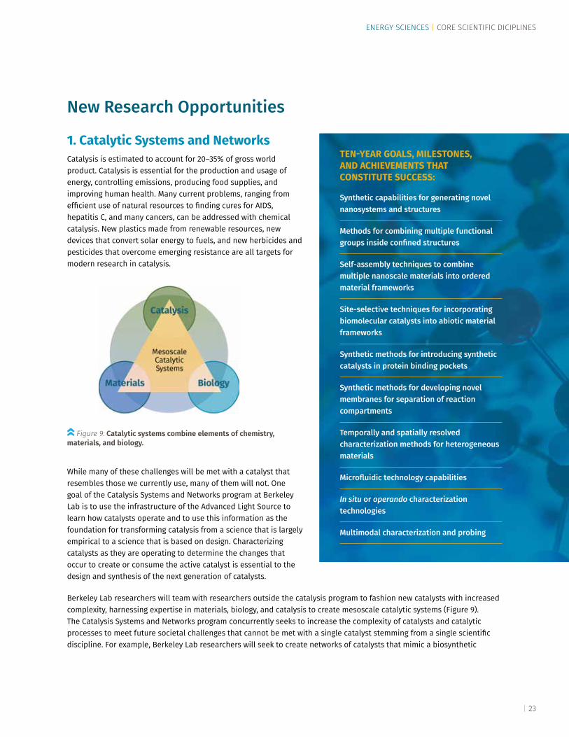
While many of these challenges will be met with a catalyst that resembles those we currently use, many of them will not. One goal of the Catalysis Systems and Networks program at Berkeley Lab is to use the infrastructure of the Advanced Light Source to learn how catalysts operate and to use this information as the foundation for transforming catalysis from a science that is largely empirical to a science that is based on design. Characterizing catalysts as they are operating to determine the changes that occur to create or consume the active catalyst is essential to the design and synthesis of the next generation of catalysts.
Berkeley Lab researchers will team with researchers outside the catalysis program to fashion new catalysts with increased complexity, harnessing expertise in materials, biology, and catalysis to create mesoscale catalytic systems (Figure 9). The Catalysis Systems and Networks program concurrently seeks to increase the complexity of catalysts and catalytic processes to meet future societal challenges that cannot be met with a single catalyst stemming from a single scientific discipline. For example, Berkeley Lab researchers will seek to create networks of catalysts that mimic a biosynthetic
TEN-YEAR GOALS, MILESTONES, AND ACHIEVEMENTS THAT CONSTITUTE SUCCESS:
Synthetic capabilities for generating novel nanosystems and structures
Methods for combining multiple functional groups inside confined structures
Self-assembly techniques to combine multiple nanoscale materials into ordered material frameworks
Site-selective techniques for incorporating biomolecular catalysts into abiotic material frameworks
Synthetic methods for introducing synthetic catalysts in protein binding pockets
Synthetic methods for developing novel membranes for separation of reaction compartments
Temporally and spatially resolved characterization methods for heterogeneous materials
Microfluidic technology capabilities
In situ or operando characterization technologies
Multimodal characterization and probing
Figure 9: Catalytic systems combine elements of chemistry, materials, and biology.

| 24
pathway via multiple steps, with a different catalyst controlling each step (Figure 10). In this way, costly and energy-intensive separations are avoided, and reactions can occur through intermediates that would be unstable as final reaction products. Likewise, researchers in catalysis will work with researchers in the Materials Sciences and Molecular Biophysics and Integrated Bioimaging Divisions to create synthetic catalysts that operate in novel environments — within a metal-organic framework or within a protein — to control the size and shape of reactants and products. At the same time, these confined systems should allow multiple types of catalysts to work together that would be incompatible when unconfined. As information is gained on such catalysts, computational methods and theoretical treatment of these systems will create the potential to design catalysts that will be the systems in use by the middle of the 21st century.
Part of the long-term vision to realize catalytic networks is to build a new laboratory space to create an environment that brings together chemists who specialize in developing novel functional materials, nanosystems, and biomaterials with chemists who specialize in the synthesis of novel catalysts and the discovery of novel chemical transformations and catalytic reactions. Berkeley Lab will leverage Laboratory facilities and other major capabilities in the Materials Sciences and Chemical Sciences Divisions for synthesis and characterization techniques that are not usually used in catalysis. See the Energy Sciences Campus section of this strategic plan on page 61.
Figure 10: Catalytic networks mimic the integrated systems of cellular processes.
An Integrated, Regulated Catalytic Network
[Au]+
intramolecularbimetalliccatalysis
M
M MM
+-
Allostericregulator
Methane, EthanePropane, renewable feedstocks, CO2, O2
Liquid fuels,alcohols, alpha olefins and arenes directlyfrom methane and light alkanes
Catalytic networkswith the components of cellular biosynthesis
inspired by microfluidic systems
Au+
Fe containing MOF+Artificialmetalloenzyme
Encapsulatedgold catalyst
Linked mesoporous system
P450 metalloenzyme
Small molecule catalystwith allosteric regulationt

ENERGY SCIENCES | CORE SCIENTIFIC DICIPLINES
| 25
2. Charge-Carrier-Driven ChemistryWhile great advances have been made in the study of charge transfer-induced excitations and chemical reactions in the gas phase and in solution, the corresponding fundamental knowledge for bulk solids, solid-solid, and solid-liquid interfaces is sparse. The pertinent length and time scales for the primary processes involved span a vast range: femtoseconds to milliseconds, and atomic bond-lengths to microns. Detailed descriptions of the pathways followed by chemical transformations induced by charge transfer, typically resulting from reduction-oxidation transitions, are unavailable for many reactions of interest so models are highly simplified and/or remain untested. The theory and experimental resources available in the Energy Sciences Area at Berkeley Lab offer a unique opportunity to develop a comprehensive understanding of the connections between charge carrier generation, recombination, energy transfer, and transport, and the mechanisms, dynamics, and efficiency of the resulting electrocatalytic and photoelectrocatalytic chemical reactions over many orders of magnitude in time and space dimensions. These studies offer an important synergistic spectrum of research that will broadly engage the Energy Sciences Area. They are also relevant to several core BES programs; capability developments at DOE national scientific user facilities; and the missions of DOE Energy Innovation Hubs at Berkeley Lab: JCAP and JCESR.
Recent advances are laying the groundwork for a comprehensive program. Atomic-scale dynamics at interfaces resulting from electronic excitations in adsorbates and semiconductor substrates have recently been followed on femtosecond to microsecond timescales. In particular, laser-pump, X-ray-probe techniques at third-generation synchrotrons and X-ray free-electron lasers (XFELs) demonstrate that specific states involved in interfacial charge transfer can be observed and identified by simultaneous, atomic-site specific probing on both sides of the interface. An example is shown in Figure 11. Electrocatalytic and photoelectrocatalytic reactions can be followed operando in electrochemical cells using tender X-rays. Theoretical techniques developed at the Molecular Foundry enable the prediction of near-edge transitions for chemically similar reactive intermediates, enabling key species to be identified. These methods probe the extrema of the space and time range: The opportunity lies in bridging them to directly identify how charge carrier dynamical processes initiate or quench specific chemical bond-making and -breaking processes, and how multiple parallel
TEN-YEAR GOALS, MILESTONES, AND ACHIEVEMENTS THAT CONSTITUTE SUCCESS:
By working broadly across chemical transformations driven by charge transfer there is an opportunity to uncover common dynamical phenomena among apparently different processes. Pathways to this goal are:
Molecular and atomic scale in situ and in operando probes of CT driven chemistry.
Bridging spatiotemporal scales to connect atomic scale electronic and chemical information with macroscopic design strategies - “full field, all time scales”.
Ability to detect rare events that represent the desired outcome, the decisive trigger, or the crucial intermediates of a chemical reaction among 1010 inactive molecules.
Time-domain experiments beyond pump-probe and photochemistry: techniques to monitor temperature-driven chemistry on fundamental time- and length-scales.
Platforms to monitor “fully dynamical” processes/devices without “steady” components, i.e. that function based on the interplay of a variety of dynamic timescales, all of which are shorter than the characteristic steady state of traditional experiments.
Monitoring emerging phenomena during synthesis.
Provide universal and multi-modal synthesis and characterization platform for (photo-)electrochemical design strategies.

| 26
pathways at complex interfaces are controlled by microscopic and macroscopic boundary conditions. As an example, photo-generated holes at the n-semiconductor (SrTiO3)/water interface initiate the water oxidation reaction. Recently, the initial time steps of this reaction have been followed dynamically with ultrafast optical and infrared spectroscopy: By targeting both sides of the interface, a surface localized Ti-O vibration was found to be excited by hole capture. Using a transient X-ray probe, the detailed molecular motions involved in this Ti-O+ vibration and their subsequent dynamics could be captured to trace out the reaction pathways involved. More broadly, studies of competing electrochemical kinetics that define branching ratios between different chemical
products in complex transformations can be envisioned. This mechanistic understanding will enable a rational approach to synthesizing materials that can utilize charge to direct chemical reactions along preferred kinetic pathways.
3. Theory of Mesoscale Chemistry The fundamental and practical importance of mesoscale science is well recognized. The functional design of materials as well as their emergent properties and modes of failure and degradation depend equally on processes that bridge many length and time scales, from the atomistic nanometer scale to the virtually macroscopic micron length scale, and beyond. Examples include harvesting artificial light to produce liquid fuels; next-generation battery technologies; and the design and assembly of advanced materials, such as metal organic frameworks, zeolites, and organic photovoltaics. These existing applications plus the vision of potential new ones lie behind the identification of mesoscale science as a new frontier for basic energy sciences, integrating chemistry, materials, and engineering.
There is an unmet need for a focused effort within mesoscale science that is not targeted at specific phenomena such as those listed above, but rather at the crosscutting theoretical problems that presently prevent the effective modeling of such phenomena. A proposed Mesoscale Theory Institute aims to address basic capability gaps in theory, which in turn can lay the basis for advances in modeling, such as new algorithms and software. Among theorists and modelers, it is widely accepted that these
Figure 11: Dentification of an intermediate interfacial charge transfer state during photoinduced charge injection from a dye into a film of ZnO semiconductor nanocrystals. Calculations (vertical colored theory bands and orbital illustrations) are employed to identify the experimentally determined chemical shift (gray band) with a charge-transfer state in which the electron is transiently retained at the semiconductor surface (Siefermann et al., J. Phys. Chem. Lett. 5, 2753 (2014); Neppl et al., Faraday Discuss. 171, 219 [2014])
Ru 3
d Ch
emic
al S
hift
(eV)
e- — h+ Separation
6
5
4
3
2
1
0
Molecular 3MLCT State
Fully Oxidized Dye
Theory
InterfacialCT State
TheoryEXPERIMENT
Theory
TEN-YEAR GOALS, MILESTONES, AND ACHIEVEMENTS THAT CONSTITUTE SUCCESS:
Modeling and understanding aerosol growth and degradation in the environment
Design and life-cycle modeling of organic photovoltaic devices
Effective catalysts for carbon dioxide reduction to fuels
Understanding regulatory networks in cells to transfer to advanced synthetic materials
Develop mesoscale design rules for complex, heterogeneous materials for energy technologies

ENERGY SCIENCES | CORE SCIENTIFIC DICIPLINES
| 27
gaps exist and are highly nontrivial. By providing the necessary foundational tools, the Institute will enable the vision of new initiatives such as artificial light harvesting, and materials and processes by design, to be realized.
Because the range of mesoscale target problems is potentially enormous, we can only name a few examples here. In all cases, the main problem is defined by the coupling between the molecular and mesoscopic scales, and theoretical methods that reach the supramolecular or mesoscale, where the limitations of size and timescales in molecular dynamics are reached, are therefore needed.
• Modeling and understanding aerosol growth and degradation in the environment: Major factors in climate models are the uncertainties associated with the properties of aerosols. Modeling at the mesoscale could help to broaden our understanding of the poorly understood history-dependent processes by which such particles grow and transform.
• Design and life-cycle modeling of organic photovoltaic devices: Organic photovoltaic materials are earth-abundant and low in energy costs to prepare, but suffer from low-efficiency (significant losses) and relatively rapid materials degradation, which represent exciting mesoscale modeling challenges with direct practical implications.
• Effective catalysts for carbon dioxide reduction to fuels: Electrocatalysis whereby the greenhouse gas, CO2, is reduced with electrons and protons to a useful fuel such as methanol by a complex process linking bulk transport, infrequent events, and reactive chemistry involving quantum mechanics of both electrons and protons, is a grand challenge in realizing the vision of photons to fuels.
• Regulatory networks in cells: Unraveling the manner in which living cells perform and modulate their activities through concentration-dependent switching and memory is an example of mesoscale emergent phenomena that, given fundamental understanding, might be transferred to advanced synthetic materials with potentially profound implications.
• Mesoscale design of energy materials: The development of chemical design rules applied to complex and heterogeneous materials would include nanoscale patterning over mesoscale assemblies of block copolymer materials, optimizing polyelectrolyte properties at solid or liquid interfaces, determining the forces governing multiphasic soft colloids, the optimal growth of quantum dots in polydisperse colloidal medium, and the chemical design of polymer electrolyte membranes (PEMs) with desirable properties.
While not comprehensive, the following lists significant capability gaps in theory, which in turn lead to gaps in modeling capabilities at and between the key length and time scales associated with mesoscale phenomena:
• Mesoscale stochastic simulation level: Stochastic simulations built on kinetic Monte Carlo models must be extended from their present domain of reaction/diffusion processes to key mesoscale processes such as materials function and degradation, modeling of electrochemical devices, and synthetic assembly at the mesoscale with full coupling of reactive chemical transformations with physical flows of heat, charge, fluid, etc.
• Bridging the scales: Well-founded methods are needed to connect continuum modeling with atomistic and ultimately electronic descriptions by providing correct up-scaling of interactions for coarse-graining, and down-scaling to perturb nanoscale and electronic environments.
• Rare events in atomistic dynamics: The billion- to trillion-fold gap between the timescale of routine events such as molecular vibrations, and rare events that initiate reactive chemical processes that manifest as emergent behavior on the mesoscale must be addressed through new advanced methods that intelligently target the bottlenecks, and thus uncover mechanism.
• Electronic level: It is an unmet challenge to accurately treat systems of significant structural and chemical complexity with mixed boundary conditions (finite, extended, and open) and a range of interactions, from physisorption to chemisorption, electronic excited states, and strong correlated ground states.
| 28
Transformative Research Facilities
The Energy Sciences Area is home to the Advanced Light Source and the
Molecular Foundry, two of Berkeley Lab’s five Office of Science national
user facilities. Along with the National Energy Research Scientific
Computing Center (NERSC), the Joint Genome Institute (JGI), and Energy
Sciences Network (ESnet), Berkeley Lab’s national user facilities serve
more than 9600 users, approximately one-third of all users of Office of
Science national user facilities. These facilities provide researchers from
around the world with the most advanced tools of modern science, and
are carefully planned and maintained to deliver the greatest scientific
impact to advance the DOE mission.
Advanced Light Source Molecular Foundry

| 29
Advanced Light Source
IntroductionThe ALS’s high-level scientific goals to achieve its vision for the future include:
Apply and further develop existing ALS tools to probe chemical, material, biological, and environmental transformations with high spatial, temporal, and spectral resolution
Collaborate with our partners to create synergy between external sponsors and the core DOE investment to develop additional world-leading beamlines and end stations
Develop a strong conceptual design and a compelling scientific case to upgrade the ALS accelerator to provide ultrahigh source brightness and to ensure world leadership in soft X-ray science in the coming decades
Functioning material and biological systems alike rely on structures that are hierarchical in space and in time. The ALS offers an unmatched suite of multiscale, multimodal imaging tools to probe such hierarchical structures in space (Figure 12), including ~1 μm resolution hard X-ray and infrared tomography, ~30 nm resolution scanning and full-field transmission X-ray microscopy, ~20 nm resolution near field infrared microscopy, and ~10 nm soft X-ray 3D ptychographic imaging with high chemical contrast. Soft X-ray (SXR) sensitivity and polarization specificity extends ALS imaging capabilities to magnetic nanostructures and domains, orbital structures in complex oxides, organic photovoltaics, and beyond. ALS tools have been applied in a pump-probe modality to study multiscale chemical and material dynamics, and the increasing soft X-ray coherent power derived from ongoing ALS accelerator improvements is being leveraged to probe a broad range of spontaneous dynamics.
Since 1993, the ALS has emerged as the world leader in soft X-ray science while also offering highly complementary infrared and hard X-ray capabilities. The facility owes its success to its deep connection to current research needs and trends as well as an outstanding user population; its strong partnership with other Berkeley Lab divisions, University of California Berkeley faculty, and beyond; continued innovation in instrumentation; increases in source stability and brightness; strong commitment to user support and collaboration; and unswerving attention to all aspects of safety. The facility supports the research of over 2,500 users per year whose ALS-based results appear in over 900 refereed journal publications annually, with over 150 articles appearing in high-impact journals. The ALS has 40 beamlines and operates more than 5,000 hours each year.
ALS has been a leader in the U.S. synchrotron community by establishing partnerships with the Department of Energy's Advanced Scientific Computational Research office facilities NERSC and ESnet, and applied mathematic resources. Those partnerships have led to the establishment of a Facility allocation of computational time at NERSC (43 million hours for 2016) that has supported over 180 users who deposited over 244,000 datasets. ALS was also instrumental in the establishment of the Center for Advanced Mathematics for Energy Research Applications (CAMERA, see page 55) in the Computing Research Division.
ENERGY SCIENCES | TRANSFORMATIVE RESEARCH FACILITIES

| 30
The ALS vision is to continue to support aggressive yet cost effective instrument development activities to address key science areas that crosscut the Grand Challenges identified by the DOE’s Basic Energy Sciences Advisory Committee (BESAC) in landmark reports from 2007 and 2015:
• Mapping electronic, ionic, and chemical pathways in catalysis, energy conversion, and energy storage: Utilize the chemical contrast and spatial resolution of spectromicroscopy to probe structure-function relationships in operating hierarchical catalytic processes and energy devices.
• Enabling the development of new functional materials for ultralow power electronics: Utilize the spatial sensitivity, spectral contrast, and temporal resolution of ring-based SXR beams in support of emerging classical, quantum, magnetic, spintronic, and neuromorphic information processing technologies.
• Illuminating the crossover between dynamics and kinetics at the nanoscale: Develop tools and protocols to understand how bond breaking and spin flips connect to activated chemical kinetics and domain wall motion, for example, to develop selective and efficient materials synthesis, self-assembly, and function.
Figure 12: ALS images spatial scales in lithium ion batteries: (a) Micron scale X-ray tomography of dendrites forming in a model lithium anode (K.J. Harry, et. al., Nature Materials 13, 69-73, [2013]). (b) Oxidation state map of a partially lithiated LixFePO4 cathode measured with a scanning transmission X-ray microscope with ~30 nm resolution (W.C. Chueh et al., Nano Letters, Jan. 30, [2013]). (c) NanoIR imaging combining infrared and atomic force microscopy sensitivities (Hans Bechtel, unpublished). (d) SXR 3D ptychographic reconstruction of grains of a LixFePO4 cathode with 18 nm resolution in all dimensions (Shapiro, et. al. Nano Letters 2015).
LFP FP
Chemical map
LiFePo4
Si
Segmented chemical mapa) d)
b) c)min max
500 nm50 µm
1 µm
LFP Mixed FP
LFP Mixed FP
y
zx
SINS
0
1.65 µm
0Fe3+ = FePO4
Fe2+ = LiFePO4
2.1 µm
4.2 770 nm
| 31
• Understanding complex biological and environmental interactions across large temporal and spatial scales: Harness the power of existing and emerging ALS imaging and spectroscopic tools to understand natural processes at their most relevant length and time scales.
• Developing experimental protocols that use high SXR coherence to understand new material phases and phenomena: Learn how to leverage phase coherence provided by modern storage ring sources to vastly improve the sensitivity, spectral resolution, and spatial and temporal dynamic range of SXR techniques.
The innovative culture of the ALS will continue unabated well into the future by continually optimizing and upgrading existing capabilities, developing new instruments to serve the evolving science needs of our diverse user community, and keeping the ALS accelerator at the state-of-the-art so as to address research areas of the future.
Current Capabilities
The ALS vision is to engage our user community to develop and apply cutting-edge tools to probe and control multiscale spatial and temporal correlations at the heart of chemical, biological, and material systems. These tools need to produce multimodal and multidimensional maps to track and understand, for example, how chemical or magnetic information is transferred between scales. The ALS now offers a suite of tools that combine structural, chemical, and magnetic contrast with the ability to map objects over exceptional size and time scales and in diverse environments: small molecule dynamics; operating electrochemical cells; cycling of batteries and fuel cells; soil samples in various states of hydration; structure and motion of protein molecules in crystals and in solution; subcellular structures, cells, tissues, and living organisms; complex electronic and magnetic material devices; and many more. These tools are under continuous development at the ALS and provide crucial capabilities to address DOE and Berkeley Lab initiatives in energy science, mesoscale science, bioscience, and beyond.
New Research Opportunities1. Mapping Chemical and Energy PathwaysDevices currently in use or being developed for selective and efficient heterogeneous catalysis, photocatalysis, energy conversion, and energy storage rely heavily on diverse multiscale phenomena, ranging from interfacial electron transfer and ion transport occurring on nanometer to picosecond scales, to macroscale batteries that charge in hours and catalytic reactors with turnover rates of ~1/sec. Soft and hard X-rays can probe dense environments with atomic and chemical contrast spanning a large spatiotemporal range, thereby providing unique fundamental information about functioning mesoscale devices. For example, ALS staff have collaborated with user groups to develop tools to map key chemical structures in batteries (Figure 12) in real time during charging cycles. Such nanokinetic measurements are essential to optimize such complex multiscale (electro)chemical devices.
The number of current ALS beamlines used for energy science and catalysis research is extensive. Many of these are among the most oversubscribed beamlines, and Table 1 indicates that our strategic priorities increase both our capability and our capacity to help users study energy conversion, energy storage, and catalytic materials.
TEN-YEAR GOALS:
Continue advancing the frontier of spatial and temporal resolution and chemical sensitivity of soft X-ray spectromicroscopy
Provide unique and world-class soft X-ray scattering techniques
ENERGY SCIENCES | TRANSFORMATIVE RESEARCH FACILITIES

| 32
Planned Capabilities
COSMIC: Since 1994, the ALS has led the world in developing soft X-ray transmission X-ray microscopes (TXMs), and scanning TXMs (STXMs). Commissioning of the COherent Scattering and MICroscopy beamline (COSMIC) in early 2016 will maintain this world leadership. One branch of COSMIC will do ptychographic diffractive imaging with state-of-the-art scanning systems, high-data-rate CCD detectors matched to a high bandwidth data system, and diverse in situ sample environments. COSMIC will provide few-nanometer resolution images, ultimately combining 3D tomographic reconstruction with full chemical contrast.
AMBER: Advanced Materials Beamline for Energy Research (AMBER) beamline will collect several spectroscopies and microscopies on a single beamline for advanced preparation and multimodal analysis of energy and catalytic systems, thereby increasing ALS capabilities and providing badly needed capacity in this area. AMBER will provide in situ sample preparation with SXE/resonant inelastic X-ray scattering (RIXS) and absorption spectroscopies, APXPS with high spatial resolution at near-atmospheric pressure, and a high throughput STXM capability.
HAXPES: The ALS has developed an intermediate energy (2-6 keV) photoemission capability on intermediate-energy beamline for hard X-ray photoelectron spectroscopy (HAXPES). In the past year staff have used this to develop the remarkable and unique capability to measure XPS spectra at an electrode surface under a thin liquid layer. This is rapidly becoming a very popular technique, particularly for the JCAP and JCESR Energy Hubs (See Section 5, Crosscutting Research Opportunities and Strategies). JCESR has recently provided funds for a new vacuum crystal monochromator.
Multimodal Scattering Techniques: RSoXS, SAXS/WAXS, Crystallography
RSoXS: The ALS RSoXS beamline was commissioned three years ago and has used the chemical contrast available near the carbon K-edge to probe organic and polymer thin films, notably the interfacial structure of organic transistors, heterojunction photovoltaics, and in self-assembled block copolymer films. It is has rapidly grown to become our most productive soft X-ray beamline. An upgrade to study liquid and complex fluid samples in several different environments is planned.
SAXS/WAXS: In the next 3–4 years, we plan to relocate the ALS SAXS/WAXS beamline to allow either sub-ms time resolved studies or higher energy resolution studies of bulk materials and thin films. The end station supports an increasingly diverse set of sample environments and leads our effort to handle large data streams. The ALS has recently formed a partnership with the Molecular Foundry to streamline access for Foundry researchers to this SAXS/WAXS beamline.
High-throughput materials crystallography: We have formed a partnership with the Molecular Foundry to enhance our materials crystallography capabilities. This will provide ~1,000 times more flux at high energy to increase capacity and precision, and to enable measuring micron-scale crystals. We will install robotic sample handling to enhance throughput and allow rapid materials screening and combinatoric experiments.
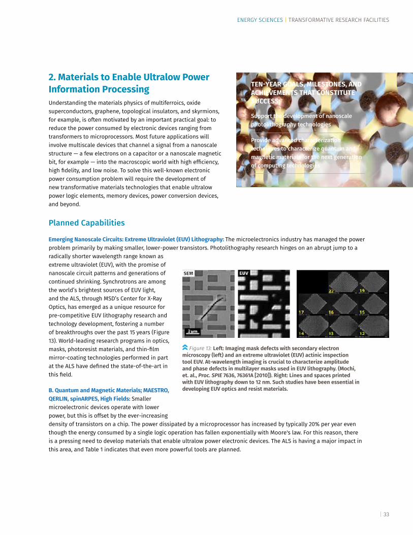
ENERGY SCIENCES | TRANSFORMATIVE RESEARCH FACILITIES
| 33
2. Materials to Enable Ultralow Power Information ProcessingUnderstanding the materials physics of multiferroics, oxide superconductors, graphene, topological insulators, and skyrmions, for example, is often motivated by an important practical goal: to reduce the power consumed by electronic devices ranging from transformers to microprocessors. Most future applications will involve multiscale devices that channel a signal from a nanoscale structure — a few electrons on a capacitor or a nanoscale magnetic bit, for example — into the macroscopic world with high efficiency, high fidelity, and low noise. To solve this well-known electronic power consumption problem will require the development of new transformative materials technologies that enable ultralow power logic elements, memory devices, power conversion devices, and beyond.
Planned Capabilities
Emerging Nanoscale Circuits: Extreme Ultraviolet (EUV) Lithography: The microelectronics industry has managed the power problem primarily by making smaller, lower-power transistors. Photolithography research hinges on an abrupt jump to a radically shorter wavelength range known as extreme ultraviolet (EUV), with the promise of nanoscale circuit patterns and generations of continued shrinking. Synchrotrons are among the world’s brightest sources of EUV light, and the ALS, through MSD’s Center for X-Ray Optics, has emerged as a unique resource for pre-competitive EUV lithography research and technology development, fostering a number of breakthroughs over the past 15 years (Figure 13). World-leading research programs in optics, masks, photoresist materials, and thin-film mirror-coating technologies performed in part at the ALS have defined the state-of-the-art in this field.
B. Quantum and Magnetic Materials; MAESTRO, QERLIN, spinARPES, High Fields: Smaller microelectronic devices operate with lower power, but this is offset by the ever-increasing density of transistors on a chip. The power dissipated by a microprocessor has increased by typically 20% per year even though the energy consumed by a single logic operation has fallen exponentially with Moore's law. For this reason, there is a pressing need to develop materials that enable ultralow power electronic devices. The ALS is having a major impact in this area, and Table 1 indicates that even more powerful tools are planned.
TEN-YEAR GOALS, MILESTONES, AND ACHIEVEMENTS THAT CONSTITUTE SUCCESS:
Support the development of nanoscale photolithography technologies
Provide advanced characterization techniques to characterize quantum and magnetic materials for the next generation of computing technologies
Figure 13: Left: Imaging mask defects with secondary electron microscopy (left) and an extreme ultraviolet (EUV) actinic inspection tool EUV. At-wavelength imaging is crucial to characterize amplitude and phase defects in multilayer masks used in EUV lithography. (Mochi, et. al., Proc. SPIE 7636, 76361A [2010]). Right: Lines and spaces printed with EUV lithography down to 12 nm. Such studies have been essential in developing EUV optics and resist materials.

| 34
MAESTRO: The angle-resolved photoelectron spectroscopy (ARPES) program at the ALS has led the world to many important discoveries related to pure and homogeneous materials, including work in high-temperature superconductivity, giant magnetoresistance, and in the discovery of the properties of graphene, topological insulators (TIs) and other exciting new materials (Figure 14). These discoveries were made possible by a continuous and ongoing program of instrumentation development in detectors, in situ sample preparation, facile data handling and analysis software, and cryogenic sample goniometry.
In the past few years, we have worked to extend this capability to probe the interplay of structure — either externally imposed through material engineering or through self-organization — with electronic properties. This has culminated in the
construction of the Microscopic And Electronic STRucture Observatory (MAESTRO) beamline (Table I), which will improve the spatial resolution available at the ALS to less than 50 nm. Coupling such a probe to extensive thin film growth and ancillary characterization tools, users will address major problems such as the origin of self-organized structures in correlated materials; the deployment of high-mobility materials such as TIs and metal-oxide heterostructures in novel device schemes; the examination of novel electronic materials such as graphene in high-field devices; the probing of multifunctional materials on the nanoscale; electronic structure of nanocrystals on an individual particle basis; and the coupling of light and electronics in emergent “plasmonic” technologies.
QERLIN: ARPES measures the coupling electrons and holes to low energy excitations, but the results are integrated over all low energy excitations. It can be difficult to verify which excitation(s) lead to a particular exotic property. To understand what drives a particular property — such as high-temperature superconductivity, for example — it is crucial to measure the dispersion relations of the low-energy excitations directly, with high-resolution soft X-ray contrast, and over a large region of Fourier space. For this reason, and also for the connection to nanokinetics discussed in the next section, one of the highest ALS priorities is to develop a soft X-ray RIXS beamline called QERLIN (Q- and Energy-ResoLved INelastic scattering). QERLIN will be based on a cutting-edge optical design that involves multiplexing the incident beam across the face of the sample, and providing tens of meV resolution with good signal in a very cost-effective approach.
High-field magnetic spectroscopy: Resonant soft X-ray spectroscopy and scattering have emerged as important tools in probing spin-, charge-, and orbital-ordered ground states of transition metal oxides, and the ALS has important capacity in this area as well. Table 1 includes an important augmentation of that capacity with an ARRA-funded superconducting octapole end station, to enable magnetic spectroscopy of oxides and hard magnet phases with fields up to 5 Tesla in arbitrary direction, thereby allowing users to probe the poorly understood anisotropy of spin- and orbital-ordered phases in complex oxides.
Magnetic STXM: An important longer-term strategic priority is to develop a flexible beamline optimized for soft X-ray spectromicroscopy of magnetic materials. Some capacity in this area resides in existing microscopes, but the difficulty of precision-control systems with variable temperature and magnetic field, as well as the difficulty of photoelectron emission microscopy (PEEM) with an applied field, seriously limits our capacity to study magnetic materials in situ and magnetic devices in operando. The COSMIC scattering branch, in Table 1 and described in more detail in the following section, will provide a valuable probe of equilibrium or steady state magnetization dynamics. The ALS is seeking funding to include in its portfolio a soft X-ray STXM dedicated to magnetic and spintronic materials (Table 1) with ~15–20 nm spatial resolution and the ability to vary temperature and applied magnetic field to image magnetic textures.
Figure 14: (a) ARPES spectrum for a homogeneous sample of graphene shows the presence of a satellite band (indicated by the black arrow) due to plasmaronic states. Bostwick et al. Science 328, 999 (2010). (b) Graphene nanostructure designed to confine plasmons (red/white arrows). Chen et al., Nature 487, 77 (2012). With spatial resolution, ARPES can be used to investigate the spatial dependence of electron-plasmon coupling.
0.05 Å-1
kX
λ0 = 9,200 nmεSiC = 2.9
λ0 = 9,681 nmεSiC = 2.0
λ0 = 10,152 nmεSiC = 0.7
E0E1E2
momentum
Ener
gy, e
V
a b
-0.5
-1.0
-1.5

| 35
ENERGY SCIENCES | TRANSFORMATIVE RESEARCH FACILITIES
3. Crossover between Atomic-Scale Dynamics and Nanoscale KineticsA hierarchy of length and time scales governs many important dynamical processes. For example, reconfiguration of small molecules often occurs on picosecond vibrational or femtosecond electronic times scales. In a protein molecule, however, ultrafast dynamics near a reaction center can be dramatically influenced by the longer-scale conformational changes of the protein backbone. Similarly, a spin flip at a magnetic domain wall can occur on the picosecond time scale characteristic of spin waves, but the domain wall moves much more slowly and the domain wall configuration helps control the flipping of a single localized spin.
Planned Capabilities
SXR Chemical Dynamics and Kinetics
In chemical reactions, the dynamic-kinetic crossover occurs roughly at a time scale of ~ 1 picosecond. A slower process is inherently kinetic and is often modeled statistically with a prefactor and activation energy. By contrast, the dynamical
oscillatory modes of a magnetic nanostructure can persist for times beyond 1 ns, and diffusive motion characterized by kinetic rate equations dominates at longer time scales. We call the regime between these dynamical and kinetic limits the nanokinetic regime, which is the focus of this third ALS research opportunity. We seek to develop soft X-ray tools to probe nanokinetics; to establish rules that govern the interplay between dynamical and kinetic phenomena; and to gain control over how a system evolves through the nanokinetic regime.
The ALS has an array of tools to undertake such studies. The productive and unique ALS Chemical Dynamics program, for example, combines ALS capabilities with resources and expertise in Berkeley Lab’s Chemical Sciences Division to serve an important and large user community. Examples of recent accomplishments include identification of the Criegee intermediate in combustion with
spectroscopy in a flame (Figure 15) and identifying a new path for hydrogen bonding and proton migration. The ALS purchased a late-model SXR monochromator from the Wisconsin Synchrotron Radiation Center, installed by the Chemical Sciences Division. A multidivisional effort led to the purchase of an ultrafast high-power laser support pump-probe system for studies of electronic and nuclear motion on the picosecond time scale.
Dynamics and Kinetics in Magnetic and Quantum Materials
Nanokinetics with COSMIC: In addition to the ptychography capability discussed above, COSMIC will also provide a branch for soft X-ray correlation spectroscopy. This will be ideal for measuring nanoscale kinetic phenomena with resonant soft X-ray contrast to probe equilibrium, steady state, and non-equilibrium processes in chemical, magnetic systems. A crucial goal is to increase the spatiotemporal dynamic range of the technique, which depends quadratically on source brightness and coherent flux.
Figure 15: The chemical reactions of Criegee intermediates, are important for atmospheric chemistry (O. Welz et al., Science 335, 224 [2012]).
TEN-YEAR GOALS, MILESTONES, AND ACHIEVEMENTS THAT CONSTITUTE SUCCESS:
Develop soft X-ray tools to probe the interaction of dynamics and kinetics in chemical reactions
Develop soft X-ray tools and techniques to understand the kinetic and dynamic evolution of magnetic systems
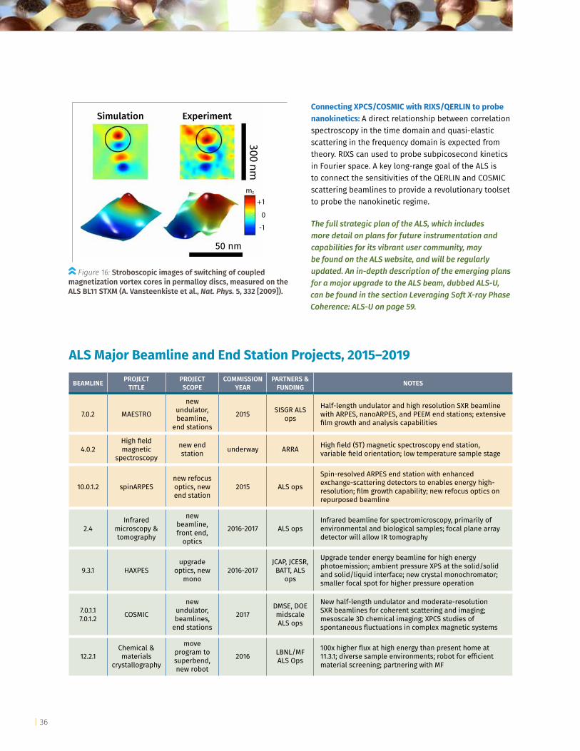
| 36
Connecting XPCS/COSMIC with RIXS/QERLIN to probe nanokinetics: A direct relationship between correlation spectroscopy in the time domain and quasi-elastic scattering in the frequency domain is expected from theory. RIXS can used to probe subpicosecond kinetics in Fourier space. A key long-range goal of the ALS is to connect the sensitivities of the QERLIN and COSMIC scattering beamlines to provide a revolutionary toolset to probe the nanokinetic regime.
The full strategic plan of the ALS, which includes more detail on plans for future instrumentation and capabilities for its vibrant user community, may be found on the ALS website, and will be regularly updated. An in-depth description of the emerging plans for a major upgrade to the ALS beam, dubbed ALS-U, can be found in the section Leveraging Soft X-ray Phase Coherence: ALS-U on page 59.
Figure 16: Stroboscopic images of switching of coupled magnetization vortex cores in permalloy discs, measured on the ALS BL11 STXM (A. Vansteenkiste et al., Nat. Phys. 5, 332 [2009]).
BEAMLINE PROJECT TITLE
PROJECT SCOPE
COMMISSION YEAR
PARTNERS & FUNDING NOTES
7.0.2 MAESTRO
new undulator, beamline,
end stations
2015 SISGR ALS ops
Half-length undulator and high resolution SXR beamline with ARPES, nanoARPES, and PEEM end stations; extensive film growth and analysis capabilities
4.0.2High field magnetic
spectroscopy
new end station underway ARRA High field (5T) magnetic spectroscopy end station,
variable field orientation; low temperature sample stage
10.0.1.2 spinARPESnew refocus optics, new end station
2015 ALS ops
Spin-resolved ARPES end station with enhanced exchange-scattering detectors to enables energy high-resolution; film growth capability; new refocus optics on repurposed beamline
2.4Infrared
microscopy & tomography
new beamline, front end,
optics
2016-2017 ALS opsInfrared beamline for spectromicroscopy, primarily of environmental and biological samples; focal plane array detector will allow IR tomography
9.3.1 HAXPESupgrade
optics, new mono
2016-2017JCAP, JCESR, BATT, ALS
ops
Upgrade tender energy beamline for high energy photoemission; ambient pressure XPS at the solid/solid and solid/liquid interface; new crystal monochromator; smaller focal spot for higher pressure operation
7.0.1.1 7.0.1.2 COSMIC
new undulator, beamlines,
end stations
2017DMSE, DOE midscale ALS ops
New half-length undulator and moderate-resolution SXR beamlines for coherent scattering and imaging; mesoscale 3D chemical imaging; XPCS studies of spontaneous fluctuations in complex magnetic systems
12.2.1Chemical & materials
crystallography
move program to superbend, new robot
2016 LBNL/MF ALS Ops
100x higher flux at high energy than present home at 11.3.1; diverse sample environments; robot for efficient material screening; partnering with MF
ALS Major Beamline and End Station Projects, 2015–2019
Simulation
50 nm
Experiment
300 nm
mz
+1
0
-1

| 37
ENERGY SCIENCES | TRANSFORMATIVE RESEARCH FACILITIES
Commission Construct Design & Procure Future planning/not funded
BEAMLINE PROJECT TITLE
PROJECT SCOPE
COMMISSION YEAR
PARTNERS & FUNDING NOTES
9.0.1 Chemical dynamics
install used SXR mono from SRC
2016 CSBG, LBNL/CSD
Configure and install modern monochromator from Wisconsin/SRC; expands chemical dynamics program into SXR regime; allows flexible studies of dynamics and kinetics
7.3.1 SXR spectroscopy
upgrade mono, restart
BL2016 JCAP, ALS
ops
Rebuild bend magnet beamline; update grating, install new slits; increases capacity for SXR spectroscopy; complements existing undulator-based capacity
5.3.1 T-REXSrepurpose beamline,
end station2016 LDRD, NIH
LBNL/PBD
Repurpose existing R&D beamline for tender energy scattering of material and biological samples; 2015 and 2016 LDRD project, new high frame rate detector supported by NIH
2.0 GEMINI
new undulator, beamline,
end station
2018HHMI, LBNL, LBNL/PBD/
NIH
High-brightness cryogenic undulator and crystal monochromator; microfocus optics into two diffractometers operating in parallel; macromolecular crystallography with small crystals and large unit cells; advanced detectors; robotic sample handling
6.0.1 QERLIN/RIXS
repurpose undulator,
new beamline and ES
2018Moore
Foundation, ALS ops
Soft X-ray RIXS beamline and end station to probe coupled excitations in complex electronic materials; double dispersion design to provide ~100x higher throughput that existing designs
6.0.2 AMBER/SXR spectroscopy
Repurpose undulator,
new beamline and ES
2018PNNL, JCAP BATT, JCESR,
ALS ops
Energy materials beamline; initially soft X-ray spectroscopy; STXM, APXPS to be developed; diverse and flexible sample environments
4.0.2 Magnetic STXM new end station 2018 NSF-MRI/
UCB?
STXM/ptychography end station for magnetic materials, complex oxides; fields to 2-3 T, variable temperature precision sample stage
4.0.2 Magnetic spectroscopy
upgrade undulator, beamline
2018 ALS ops
Upgrade 16 year old beamline, 10x more flux and much higher brightness at ALS; ALS-U ready; modern monochromator; optics upgrade; optimized undulator period
SAXS move 7.3.3
SAXS/WAXS to SB/wiggler
2018 ALS ops
Move existing SAXS beamline to a SB; 100x increase in flux and capacity; increase time resolution and install crystal monochromator for lower energy band width; diverse sample environments.
Nano-spinARPES planning 202x LDRD
With LDRD support, ALS is planning to combine growing expertise in nanoARPES with advanced spin detectors to probe the spin structure in nano-devices and nano-structured materials. Benefits heavily from ALS-U
9.0 Chicane sector, update optics planning 202x
Doubles capacity and serves VUV and soft X-ray chemical dynamics/kinetics beamlines; a key part of ALS-U planning; will need to wait to on-axis injector so a new class of high brightness undulator can be deployed
10.0Chicane
sector, update beamlines
planning 202x
Increase ARPES capacity; likely home for nano-spinARPES above; a key part of ALS-U planning; will need to wait to on-axis injector so a new class of high brightness undulator can be deployed
8.0Chicane
sector, update beamlines
planning 202xTwo high performance undulators for soft and intermediate energy spectroscopy and microscopy; probably done in sync with ALS-U

| 38
The Molecular Foundry
IntroductionThe Molecular Foundry’s broad institutional goals are to:
Be a world-leading center of excellence for nanoscience, producing and enabling impactful user-inspired research in innovative materials synthesis, advanced electron and optical characterization, and predictive theory and modeling.
Attract and foster strong collaborations with outstanding users from academia, industry, and government laboratories worldwide. Provide all users with world-class facilities and a one-of-a-kind expertise, both at the Foundry and within the Berkeley Lab environment, working together to identify and address the biggest challenges in nanoscale science.
Play a central leadership role at Berkeley Lab in materials science, and serve as a conduit for high-resolution imaging; organic, inorganic, and biological synthesis; and computational efforts.
Influence, educate, and train the next generation of interdisciplinary scientists who will carry forward Foundry expertise and safety culture throughout their careers at other institutions and in industry.
The Molecular Foundry’s mission is to provide users worldwide with access to expert staff and cutting-edge instrumentation to enable the understanding and control of matter at the nanoscale in a multidisciplinary, collaborative environment. The 2014 consolidation of the Molecular Foundry and the National Center for Electron Microscopy (NCEM) is an exciting new chapter that brings the Foundry to the forefront of electron microscopy and provides an opportunity to develop and harness entirely new approaches to high-resolution, time-resolved, and in situ electron scattering of hybrid materials. NCEM becomes the seventh facility at the Foundry by joining the existing facilities specializing in Imaging and Manipulation of Nanostructures; Nanofabrication; Theory of Nanostructured Materials; Inorganic Nanostructures, Biological Nanostructures; and Organic and Macromolecular Synthesis. In 2015, the Molecular Foundry hosted a total of 677 on-site users, and published 321 journal articles.
The Molecular Foundry’s vision is to provide multidisciplinary communities of users the opportunity to develop, probe, understand, and control matter and its behavior at nanometer length scales to address the most important technological challenges in energy and the environment.

| 39
ENERGY SCIENCES | TRANSFORMATIVE RESEARCH FACILITIES
Current Capabilities
The six-story, 94,000-square-foot Molecular Foundry building at Berkeley Lab overlooks the UC Berkeley campus and, from a distance, the San Francisco Bay. Directly adjacent to the Foundry is the NCEM complex that was established in 1983 to maintain a forefront research center for electron microscopy of materials with state-of-the-art instrumentation and expertise. NCEM at the Foundry features 10 electron microscopes, many of which are world-leading. Each of the six floors of the Foundry building, as well as NCEM, is managed as a technically distinct “facility” by world-class scientists equipped with state-of-the-art instrumentation, laboratories, and computational resources.
Imaging and Manipulation of Nanostructures
This facility develops and provides access to state-of-the-art characterization and manipulation of nanostructured materials — from “hard” to very “soft” matter — including electron, optical, and scanning probe microscopies.
Nanofabrication Facility
This facility focuses on understanding and applying advanced lithographies; and thin-film deposition and characterization, emphasizing the integration of inorganic, organic, and biological nanosystems with the potential for nanoelectronic, nanophotonic, and energy applications.
Theory of Nanostructured Materials Facility
This facility expands our understanding of materials and phenomena at the nanoscale through the development and application of theories and methods for excited-state and charge transport at nanoscale interfaces, self-assembly of nanostructures, and X-ray spectroscopy in complex nanostructured systems.
Inorganic Nanostructures Facility
This facility is devoted to the science of semiconductor, carbon and hybrid nanostructures— including design, synthesis, and combinatorial discovery of nanocrystals, nanowires, and nanotubes and their self-assembly into 3D mesoscale functional materials for use-inspired energy applications.
Biological Nanostructures Facility
This facility designs and synthesizes new materials based on the self-assembly of biopolymers and bio-inspired polymers, creates new nanocrystals probes for bioimaging, and develops synthetic biology techniques to re-engineer organisms and create hybrid biomolecules to interface with a variety of applications.
Organic and Macromolecular Synthesis Facility
This facility studies “soft” materials, including the synthesis of organic molecules, macromolecules, polymers and their assemblies, with access to functional systems, photoactive materials, organic-inorganic hybrid structures, and porous materials.
National Center for Electron Microscopy (NCEM)
This world-renowned center for microscopy features cutting-edge instrumentation, techniques and expertise required for exceptionally high-resolution imaging and analytical characterization of a broad array of materials.

| 40
New Research Opportunities1. Combinatorial Nanoscience Combinatorial nanoscience focuses on the rational design of targeted nanostructured materials. Robotic synthesizers are used to generate large libraries of biological, organic, and inorganic nanostructures, which, in combination with theory and characterization, are used for discovery of new materials with sought-after optical, electronic, and thermal properties — see for example, Figure 17. This has required the development of a comprehensive suite of one-of-a-kind tools that are used in concert with theoretical predictions and scientific intuition. To date, these methods have been applied with substantial success to the discovery and optimization of new biomolecular assemblies, biomimetic polymers, inorganic nanocrystals, and metal-organic frameworks. The large datasets produced by these efforts are also guiding the development of new theoretical methods and tools (e.g., new force fields) to predict the properties of yet-uncharted nanomaterial compositions.
Although the morphologies of nanomaterials can be used to dictate some of their characteristics, controlling the three-dimensional positions of heteroatoms, domains, and functional groups within them can arguably specify an even richer set of properties. As examples, the precise location of dopant atoms within nanocrystals can lead to new photophysical properties, and specific combinations of organic functional groups can lead to highly selective catalysts. To access nanomaterials with this level of structural sophistication, multistep chemical syntheses must be used to “program” the assembly of heterogeneous components in a particular order. By using our customized robotic tools to navigate sequences of synthetic parameters in systematically varied combinations, we have identified useful synthesis pathways that are often complex, highly interdependent, and non-intuitive. User demand for these specialized tools is rapidly growing and regularly exceeds capacity.
To create functional mesoscale materials with ever-increasing complexity, we must be able to predict the assembly pathways of heterogeneous building blocks as well as the new properties that will emerge. We will achieve this by integrating deliberately synthesized and well-defined building blocks from combinatorial methods, and harnessing the Foundry staff’s considerable expertise in synthesis, assembly, characterization, and theory over multiple length scales, as well as those characterization capabilities of the ALS.
We aim to become the premier facility for designing, synthesizing, and purifying sequence-specific polymers, characterizing and understanding their rules of folding and assembly, and creating nanostructured materials capable of complex, protein-like functions (e.g., molecular recognition and catalysis). Predictive multiscale simulations will allow us to design new polymers that fold and self-assemble into well-defined ion channels, specific binding pockets, and efficient catalytic sites.
TEN-YEAR GOALS, MILESTONES, AND ACHIEVEMENTS THAT CONSTITUTE SUCCESS:
Predict the assembly pathways of heterogeneous building blocks and the new properties that will emerge from these functional mesoscale materials
Become the premier facility for designing, synthesizing, and purifying sequence- specific polymers

| 41
ENERGY SCIENCES | TRANSFORMATIVE RESEARCH FACILITIES
Planned capabilities:
• High-pressure, high-temperature, multistep robotic synthesizer: Our capabilities in high-throughput colloidal nanocrystal synthesis will be significantly enhanced with our next-generation nanocrystal synthesis robot — the High-throughput Experimentation Robot for Multiplexed Automation of Nanochemistry (HERMAN) and the hiring of new staff in the Inorganic and Organic Facilities. Using machine-learning algorithms closely integrated with theoretical models, HERMAN will perform automated multistep chemical synthesis at unprecedented temperatures and pressures.
• Microfluidic platforms for parallel synthesis and characterization: As characterization techniques are developed that use ever-smaller amounts of material, we will miniaturize biopolymer and nanocrystal synthesis reactions by using a suite of microfluidic equipment. For example, we will develop “smart” synthesis chips that use in situ data analysis to perform both synthesis and screening. This will enable thousands of compounds to be prepared and screened in parallel, and thus accelerate the discovery of next-generation nanomaterials.
• High-throughput characterization: We aim to establish automated electron microscopy methods that leverage NCEM’s expertise in electron microscopy, take advantage of X-ray scattering capabilities at the ALS, and pursue electrochemical and spectroscopic approaches to evaluate hundreds of samples with minimal human intervention post-synthesis. Furthermore, we will benefit from close connections with applied mathematicians at Berkeley Lab through the new Center for Applied Mathematics for Energy Research Applications (CAMERA) to help build screening methods and bring tools of computational geometry, optimization, and machine learning.
Figure 17: A diversity of nanomaterial discovery platforms under study at the Molecular Foundry.
Biomolecularelectron
nanoconduits
Inorganicnanocrystals
Metal-organicframeworks
Mesocalecomposites
Protein-mimeticpolymers

| 42
2. Functional Nanointerfaces A frontier in materials science, and an area of increasing user interest, is the controlled integration of diverse nanoscale building blocks — such as inorganic, organic, and biological — into functional nano- and mesoscale assemblies, depicted in Figure 18. As nanostructured building blocks intrinsically possess large surface-to-volume ratios, their assemblies feature a high-density nanoscale network of nanoscale interfaces that present exciting new opportunities to control the propoagation of energy in hybrid materials. The goal is to develop capabilities for the discovery, understanding, and design of novel functional nanostructured materials from the perspective of their component interfaces. This effort aims to harness their unique characteristics, both individually and collectively, for emergent functionalities, particularly for energy conversion, storage, and conservation.
Interfaces can actively amplify or hinder the motion of charges, vibrational energy, light, or chemical information due to sharp contrasts in bonding modes, electronic energy levels, and densities of states. There is much to learn about the exact nature of these emerging structural, electronic, and dynamic properties and how they feed back across multiple length scales. However, a rich set of interdisciplinary scientific problems involves active transport processes at organic/inorganic, bio/inorganic, solid/electrolyte, and gas/solid interfaces. This theme involves crosscutting activities spanning the creation of bottom-up 3D functional mesoscale assemblies with precisely controlled interfaces; the development of new theoretical frameworks and computational tools for understanding and predicting static and dynamic properties of these interfaces; mapping chemical transformations and energy
flow across scales using advanced electron microscopy and the ALS; and detailed imaging and transport studies at these complex, buried, and dynamic interfaces.
Over the next few years, we will advance our ability to chemically introduce orthogonal surface chemistries on arbitrary materials classes to enable new heteromaterial couplings. We will also advance in situ imaging capabilities for both hard and soft matter at various length scales and in relevant sample environments. At the same time, we will utilize atomic force microscopy (AFM) as well as new approaches in advanced electron microscopy and scattering, and leverage the relevant capabilities of the ALS.
Metal chalcogenides are a broad material class of considerable interest for their diverse electronic, optical, mechanical, and catalytic properties. Examples include high-mobility semiconductors, superionics, high-Tc superconductors, and topological insulators. Metal-organic chemical design affords an opportunity to build hybrid nanomaterials that link the structure of the supramolecular lattice to the function of the inorganic scaffold. Crystal engineering in the context of this approach will yield the capability to design and engineer the band structure of semiconducting materials with atomic precision. The central challenge is disentangling the complex structure-function relationships governed by metal coordination, ligand shape, and composition. A collaborative effort between the Inorganic Nanostructures Facility, Theory of Nanostructured Materials Facility, and ALS Beamline 11.3.1 will design, construct, characterize, and redesign metal-organic chalcogenide nanomaterials over a broad composition range.
TEN-YEAR GOALS, MILESTONES, AND ACHIEVEMENTS THAT CONSTITUTE SUCCESS:
Enable new heteromaterial couplings by advancing our ability to chemically introduce orthogonal surface chemistries on arbitrary materials classes
Advance in situ imaging capabilities for hard and soft matter at various length scales and in relevant sample environments
Design, construct, characterize, and redesign metal-organic chalcogenide nanomaterials over a broad range of compositions, in partnership with the ALS
Elucidate design rules governing how individual components of arbitrary shape, size, and composition are assembled and ultimately interfaced.
Develop capabilities that link the Molecular Foundry’s computational simulations and in situ X-ray tomography capabilities with the ALS’s X-ray scattering instrumentation

| 43
ENERGY SCIENCES | TRANSFORMATIVE RESEARCH FACILITIES
In the next five years, we will focus on elucidating the design rules by which desired functionality can be generated by exerting precise control over how individual components of arbitrary shape, size, and composition are assembled and ultimately interfaced. We will develop capabilities that link, for the first time, the Molecular Foundry’s computational simulations with the ALS’s X-ray scattering instrumentation and NCEM’s in situ X-ray tomography capabilities.
Planned capabilities:
• Joint Molecular Foundry–ALS small- and wide-angle scattering beamline: We will partner with the ALS to set up a dedicated beamline for Foundry users with advanced high-flux SAXS/WAXS capabilities for determining the nanoscale and mesoscale structure of soft and hybrid nano- and mesostructured materials.
• In situ combinatorial electrochemical interface imaging and analysis end-station: We will develop a suite of coupled in situ tools capable of probing both structure and transport at individual solid/electrolyte interfaces and across statistical ensembles of interfaces in reactive environments. Understanding how interfaces influence chemical confinement, concentration fluctuations, and transport across these complex interfaces will serve crucial needs demanded by our global network of users and also other local synergistic DOE investments such as the Materials Genome Initiative, Joint Center for Artificial Photosynthesis (JCAP), and Joint Center for Energy Storage Research (JCESR).
• Mesoscale theory for functional nanointerfaces from electrons to assemblies: Our aim of understanding materials and phenomena from the scale of electrons to assemblies requires us to tackle head-on the mesoscale challenge that is the coupling of distinct physical mechanisms across a broad range of length and time scales. To do so we will bridge our current many-scale theoretical capabilities in electronic structure and statistical mechanics — employing state-of-the-art mid-range cluster computing — toward an integrated predictive multi-scale simulation framework.
Figure 18: The Molecular Foundry’s synthesis and fabrication capabilities provide controlled approaches to create multidimensional interfaces spanning the nanoscale. Colloidal nanocrystals have insulating, inert coatings, which prevent easy coupling of nanocrystals for energy transfer. Naked nanocrystal building blocks can be assembled into molecular, nano, or mesoscale composites with nanoscale interfaces of controlled dimension and functionality.
Nanointerfaces by design using naked building blocks
, , ...
3D interfacial networks — nanocomposites
ligand stripping functionalization for assembly
molecular
~1 nm ~10 nm ~100 nm
nanoscale mesoscale

| 44
3. Multimodal Nanoscale Imaging We will develop and apply multiple spectroscopic and imaging technologies — including high-resolution flagship electron microscopies, scanned probe microscopies, and hyperspectral (nano)optical methods and imaging probes — to investigate structural and dynamic nanoscale phenomena in hard and soft nanostructured materials in solid-state, liquid, and vapor environments. This theme takes on the characterization challenges associated with the continued development of novel and increasingly complex hybrid materials.
Visualizing structure, and correlating it with properties and mechanisms at meso- and nanoscopic length, time, and energy scales under operating conditions is both an enabling tool and
grand challenge for nanoscale science, as emphasized by the 2014 DOE report, Future of Electron Scattering & Diffraction. This theme investigates nanoscale systems in complex cellular, solid- state, liquid, or gaseous environments, increasingly in relevant working conditions – for example, under bias, strain, or illumination – and thus focuses on the development of new technologies for in situ techniques. Our goal is to explore the basic principles underlying functionality by correlating chemical composition, spectroscopic and mechanical properties, and nano- and mesoscale morphology, and to enable burgeoning areas of user research.
Unraveling the relationships between material composition, morphology, and function raises a number of fundamental scientific questions. For example, many of the synthesis efforts of Molecular Foundry users involve non-equilibrium systems that assemble dynamically and are responsive to changes in local environment. Understanding fundamental mechanisms of growth and evolution often require combined methods that can reveal the properties of materials in situ, explaining their growth or failure mechanisms, even when it necessitates an atomic-scale understanding (provided by in situ electron microscopy) to couple with a macroscopic phenomenon. We aim to approach these challenges via (1) complementary multimodal characterization and (2) the development of instrumentation that can follow the dynamic evolution of parameters with the critical time resolution.
In order to engineer revolutionary materials with new behaviors, we need first to understand the fundamental structure-property-function relationships in material and biological systems with abundant interfaces, and with interwoven heterogeneity and order on multiple length scales. The goal of probing buried interfaces (e.g., well beyond an extinction depth) also extends to the problem of nanoparticle nucleation or live cellular dynamics in liquid environments to enable imaging of individual components of nuclei or live cells with increasing speed and resolution.
TEN-YEAR GOALS, MILESTONES, AND ACHIEVEMENTS THAT CONSTITUTE SUCCESS:
Imaging function and interactions in buried interfaces
Mapping fields in space and time through multimodal and multidimensional imaging techniques
Figure 19: Encased AFM cantilevers provide exquisite sensitivity and resolution for in situ investigation of material interfaces (Ziegler, et a. MEMS 131, 128 [2014] DOI: 10.1109/MEMSYS.2014.6765590).

| 45
ENERGY SCIENCES | TRANSFORMATIVE RESEARCH FACILITIES
The development of new multimodal and multidimensional imaging techniques involve collecting radically new quantities of data — N-dimensional spectra — and we will address head-on the management, searching, and indexing of this “big data.” Experimental development efforts involving spectroscopy in the time-domain will require significant developments in theory and simulation of excited states to model realistic pumped and/or probed excited states in nanoscale systems and at interfaces.
Planned capabilities:
• Nanoscale spectroscopic imaging of subsurface interfaces and defects: We will develop minimally
invasive technologies able to probe the structure, electronics, and bonding of complex buried interfaces and deep-tissue biological structures, revealing previously unobserved and emergent functionality; additionally coupling with ALS-based efforts to study the entire span of mesoscopic time and energy scales. We will also couple recent breakthroughs in photoacoustic microscopy — which combines deeply penetrating near-infrared (NIR) excitation and acoustic response, even within dense, highly scattering media — with cutting-edge Molecular Foundry NIR nanocrystal probes, allowing us to understand the physical properties of matter at deeply buried structures and interfaces with nanoscale or subcellular resolution.
• Multimodal high-resolution in situ transmission electron microscopy: Building off of the success of the TEAM project, and current efforts in atomic resolution tomography and in situ microscopy, the development of a multimodal in situ transmission electron microscope (TEM) will combine imaging with optical, X-ray, and electronic spectroscopies at atomic resolution under chemical, electrical, optical, thermal, magnetic, and other stimuli. Multidimensional imaging of dynamic processes such as nucleation and transformation at the atomic scale will require dedicated electron microscopy instrumentation and technique development to increase image contrast, energy and time resolution, signal detection, sample environment, and probing capabilities.
• Mapping dynamics in soft and hybrid materials: We plan to investigate exciton and photon transport using spatially independent excitation and probing with localized excitation photo current microscopy (LEPCEM) and with combined cathodoluminesence excitation and near-field optical probing. Concomitantly, we will develop tools to watch biological, soft, and hard material components as they dynamically combine and reorganize upon assembly with real-space in situ AFM/TEM and cryo-EM methods. We will build on our spin-polarized low-energy electron microscope (SPLEEM) expertise and instrumentation to image the distribution of charge and evolving transport pathways in soft and hybrid organic-inorganic semiconductor systems in situ and without damage. We will further develop near-real-time individual particle electron tomography with advanced electron detectors.
Figure 20: Schematic of the so-called “Campanile” microscopy tip (left) that reveals both shape and chemistry of a nanowire (right) (Bao, et al. Science 338, 1317 [2012] DOI: 10.1126/science.1227977).
PL in
tens
ity
(pea
k no
rmal
ized
to 1
)
780 800 820 840 860 880 wavelength (nm)
KCs5
3
0

| 46
4. Single-Digit Nanofabrication and Assembly We aim to organize and structure material with critical features of dimensions at or below 10 nm, i.e., on the single-digit nanometer and atomic scales, to create nanoscale devices and architectures in inorganic, biological, or hybrid systems. We will accomplish our goals by developing protocols to both understand and implement methods of self-assembly and lithography in a variety of systems.
We will also develop a fundamental understanding of, and design principles for, the way components — atoms, molecules, nano- and bulk materials — can be structured and assembled with “single-digit-nanometer” precision. Addressing this challenge requires an understanding of the mesoscale coupling of atomic-scale interactions with assembly-scale manipulation and driving protocols. This understanding will then be used to promote breakthroughs in fundamental understanding and control in areas of technological interest such as solar energy conversion, energy storage, light-based communications, data storage, and catalysis. Building on the Foundry’s expertise in bottom-up (self-assembly) and top-down (lithography) nanofabrication — among the Foundry’s most heavily demanded capabilities — we will advance
the forefront of fabricating novel devices. Major goals include addressing the Grand Challenges of 3D nanofabrication, and understanding and controlling the far-from-equilibrium guided assembly of multicomponent systems composed of biological, organic, inorganic, and hybrid materials.
Molecular Foundry researchers continue to advance the science of ultrathin 2D assemblies of organic materials. These 2D polymers are assembled as discrete sheets, and are comprised of one or more monomer units. They exhibit both regular periodicity and long-range in-plane order. The connectivity between building blocks within each 2D organic layer can be either covalent or noncovalent. The layer thicknesses of these 2D structures are typically a few nanometers, corresponding to the size of a single molecule or a few well-packed molecules, and are generally several orders of magnitude smaller than the lateral dimension. The ability to synthesize precisely defined 2D organic layers is expected to expand the already rich functionality of conventional 1D linear polymers. Foundry scientists are making great progress in achieving better control of the design and synthesis of 2D structures, including control over the exact pore size, shape, and functionality over a large area, and are engineering functionality in both homogenous and heterogeneous molecular nanosystems. Emerging applications of these materials include their use in membranes, storage materials, sensing, catalysis, and optoelectronic devices.
Combining traditional tools of top-down nanofabrication with directed self-assembly, we aim to create complex functional structures that are uniquely patterned in all three spatial dimensions with single-digit nanometer control enabled by bottom-up approaches. Such 3D structures and assemblies will open up new applications for guiding the flow of energy, light and chemical reactants and products. For instance, we will develop wafer scale processing of transition metal dichalcogenide heterostructures to build layered systems with engineered bandgaps that can direct electron flow. In addition, we will use sequential nanoimprint lithography with functionalized resist with precision alignment to create novel complex metamaterials and other light-guiding systems. We will create the highest quality scanning probes with new ion beam lithographies. Using novel scanning probes and two-photon lithography, we will explore new routes for writing 3D structures.
TEN-YEAR GOALS, MILESTONES, AND ACHIEVEMENTS THAT CONSTITUTE SUCCESS:
Advance the science of precision two-dimensional assembly
Create complex functional structures uniquely patterned in all three spatial dimensions with single-digit nanometer control enabled by bottom-up approaches
Develop new theoretical approaches and fabrication strategies to understand how component shape, chemical functionality, chemical transformations, and the flow of energy influence the organization of materials into structures far from equilibrium

| 47
ENERGY SCIENCES | TRANSFORMATIVE RESEARCH FACILITIES
While huge advances have been made in guided assembly of single component systems at or near equilibrium, remaining challenges are to understand and control the assembly of heterogeneous structures far from equilibrium.
We will develop new theoretical approaches and fabrication strategies to understand how component shape, chemical functionality, chemical transformations, and the flow of energy influence the organization of materials into structures far from equilibrium. In parallel, we will structure heterogeneous devices with controlled surface chemistry, topology, and nanometer-scale feature sizes to replicate the virtual environments developed for simulation and theoretical modeling of assembly. Using multimodal imaging techniques, we aim to observe assembly in real-time to validate and refine theoretical models.
By fabricating assembly environments with more complexity, we can study how energy in the form of localized radiation, concentration, and temperature gradients influence self-assembly.
Planned capabilities:
• Wafer-scale processing of transition metal dichalcogenides (TMDs) by atomic layer deposition (ALD): Two-dimensional monolayer TMD films (e.g., MoS2, WS2, and MoSe2) have recently been shown to possess both high-field effect mobilities and a direct band gap in the visible, opening the possibility of exploring new classes of optoelectronic structures and basic physical phenomena. We are currently investing in the development of a new type of TMD deposition process that uses ALD processes, maintaining the advantageous properties of ALD (scalability, conformality, and thickness and composition control).
• High-resolution 3D lithography and precision-aligned nanoimprinting: A two-photon lithography system, modified to incorporate Foundry-developed sub diffraction limited nano-optics, would push the resolution of the 3D features into the single-digit nanometer range. Nanoimprint capabilities provide a means to replicate over-and-over single digit nano templates created using other lithographic techniques. With alignment, nanoimprinting will be expanded to fabricate integrated devices and complex 3-D structures and probes with high volume. In combination, this suite of technologies will be used to build probes for multimodal imaging and tip-based lithography, while its advanced imaging capabilities can be used to study and screen nanomaterials as part of the Molecular Foundry’s combinatorial efforts.
• Simulation and dynamic imaging of self-assembly: Understanding the process of materials creation requires an ability to dynamically observe components as they combine and rearrange to produce a desired structure. To achieve these goals, real-space in situ AFM and TEM methods will be used, in tandem with far-from-equilibrium theories of self-assembly to guide the assembly of undriven systems that are prone to kinetic trapping (such as multicomponent mixtures), and of intrinsically nonequilibrium systems (such as those subjected to spinning and drying). Visualization tools include our multimodal imaging methods, particularly the 3D tomographic methods that build on the extraordinary performance of existing aberration-corrected electron microscopes and the gentle encased cantilevers for in situ high resolution imaging. We will further develop multiscale simulation tools to model and thereby infer structure across multiple length scales from time-dependent scattering measurements at the ALS.
The full strategic plan of the Molecular Foundry, which includes more detail on plans for future instrumentation and capabilities for its vibrant user community, may be found on the Molecular Foundry website, and will be regularly updated.

| 48
Crosscutting Research Opportunities and StrategiesRecent DOE funding opportunities have emphasized the importance of
team-based approaches to tackling the most critical challenges in energy
science research. The Energy Innovation Hubs are integrated research
centers that combine basic and applied research with engineering to
accelerate promising energy science solutions beyond basic research
toward economic viability. Berkeley Lab is a key partner in two hubs: the
Joint Center for Artificial Photosynthesis (JCAP) and the Joint Center for
Energy Storage Research (JCESR).
Another DOE program focused on team science is the Energy Frontier
Research Centers (EFRC) program, which supports teams of researchers to
pursue fundamental research that addresses both energy challenges and
the scientific Grand Challenges underpinning emerging energy solutions.
Berkeley Lab is the lead institution for the Nanoscale Controls on Geologic
CO2 (NCGC) EFRC, and is a key participant in the Center for Gas Separations
Relevant to Clean Energy Technologies (CGS) led by the University of
California, Berkeley.

| 49
ENERGY SCIENCES | CROSSCUTTING RESEARCH OPPORTUNITIES AND STRATEGIES
Energy Innovation Hubs
Modeled after the scientific management structure of the Manhattan Project and AT&T Bell Laboratories, DOE’s Energy Innovation Hubs are integrated research centers that accelerate scientific discovery to address critical energy issues through teams of scientists focused on all stages of research and development.
Fuels from Sunlight ResearchJCAP OverviewJCAP’s mission is directly linked to understanding the fundamental science of photoelectrochemical transformations:
• Photoelectrochemical catalytic networks: Design and synthesis of photoelectrochemical catalytic networks to actively control multi-electron, multiproton reaction pathways to generate any desired reaction product with complete selectivity and high efficiency.
• Water oxidation systems with living cells: Development of methods for integrating robust artificial light capture/photo-electrochemical water oxidation systems with living cells for heavy (high-carbon) liquid fuel production.
• Solar photo-electrochemical synthesis of fertilizers: Build on discoveries in solar fuels research to develop solar photo-electrochemical synthesis of fertilizers such as ammonium nitrate and phosphates from air- and water-borne sources.
The Department of Energy’s substantial investment in the Joint Center for Artificial Photosynthesis (JCAP) has established a superbly equipped, state-of-the art facility now located on the main Berkeley Lab campus. This facility can support fundamental and applied research in solar fuels and related areas built on the use of photovoltaic devices. JCAP thrives as a multidisciplinary center with a strong team culture, spanning four areas and five divisions at Berkeley Lab.
JCAP has focused on developing synergistic partnerships with several of the Northern California national scientific user facilities: the ALS, the Stanford Synchrotron Radiation Lightsource (SSRL), and the Molecular Foundry. The scope of existing and planned programs at each facility — an Approved Program at the ALS, a Cooperative Agreement Proposal at SSRL and a Partner User
GOALS, MILESTONES, AND ACHIEVEMENTS THAT CONSTITUTE SUCCESS:
Understand the relationship between electron dynamics, coupled charge transport, and catalytic chemistry.
Determine the scientific basis of activity of 4-metal catalyst systems.
Design and understand nanostructured assemblies for efficient charge carrier formation and transport from light absorber to catalyst.
Develop time-resolved studies of operando dynamics of the sequences of intermediates in multi-electron processes.
Develop computational methods that link atomistic theoretical descriptions to operando experimental observations.
Understand the correlation between transport of gases and chemical species, and polymer architecture and thin-film superstructures in membranes.
Develop high-throughput theoretical methods that are predictive for solid-solid and solid-liquid interface structure and energetics.
Develop theory and measurement of ultraslow, stochastically driven, irreversible displacement of atoms in solids

| 50
Program at the Molecular Foundry currently under development — is fully coordinated with the programs of the others. The scientific work often involves interfacility collaborations, and is focused on developing techniques and capabilities in electrochemistry and high-throughput measurements.
Research Opportunities
The conversion of atmospheric carbon sources such as CO2 into a feedstock for useful energy chemicals offers a closed-cycle solution to meet society’s needs with minimal impact on the Earth’s systems. Current research into the use of sunlight and CO2 to generate small molecules such as methanol and methane using simple photo-electrochemical cells, already very challenging, is only a starting point. Building on the critical mass of expertise recruited into JCAP, we envision expansion into research areas in which our approach will emphasize linking component discoveries to the creation of functioning nanoscale- to centimeter-scale systems.
Successful approaches to our Grand Challenges will require discovery of new catalysts, membranes, mechanisms for concentrating diffuse sources of reactants, and methods for moving and releasing reaction products. Exquisite control of these processes will be required to ensure ongoing function with degradation on the timescale of years in an intensely reactive environment. Work on photoelectrodes may also be required, but JCAP’s successes in developing versatile photoelectrode architectures and components can serve as an initial foundation.
JCAP’s rapid progress in translating discoveries into working devices has opened science opportunities related to catalytic and electrochemical reactions that are presently outside JCAP’s mission and scope but are likely to be deeply transformative. These opportunities represent potential 10-year goals for photoelectrochemical research that builds on the first two phases of the JCAP Hub at Berkeley Lab.
Improved understanding in these areas will have impacts beyond electrochemical and photoelectrochemical processes, extending into earth sciences, soft matter science, and condensed matter physics, for example.
Energy Storage ScienceJCESR OverviewThe Joint Center for Energy Storage Research (JCESR), a collaboration with Argonne National Laboratory, Berkeley Lab, and other institutions, has the objective of overcoming fundamental scientific challenges and enabling next-generation, beyond-lithium-ion energy-storage systems. The JCESR will pursue advanced scientific research to understand electrochemical materials and phenomena at the atomic and molecular scale, and to use this fundamental knowledge to discover and design next-generation energy-storage technologies. The ability to understand materials and chemical processes at a fundamental level should enable technologies beyond traditional lithium-ion batteries and store at least five times more energy than today’s batteries at one-fifth the cost. JCESR researchers already understand the fundamentals of magnesium-ion transport in solid lattices, and are developing insights to enable multivalent-ion batteries.
JCESR’s paradigm replaces Edisonian science with innovative new tools that map the broad outlines of the beyond-lithium-ion landscape instead of laboriously exploring its details one battery
GOALS, MILESTONES, AND ACHIEVEMENTS THAT CONSTITUTE SUCCESS:
Library of fundamental knowledge of the materials and phenomena of electrical energy storage at the atomic and molecular levels
Creation of two prototypes for transportation and grid energy storage solutions
Create a new paradigm for battery research and development that accelerates the pace of discovery and innovation, and reduces the time from conceptualization to commercialization.

ENERGY SCIENCES | CROSSCUTTING RESEARCH OPPORTUNITIES AND STRATEGIES
| 51
system at a time. These new tools include the Materials Project, the Electrolyte Genome, the Electrochemical Discovery Laboratory, and Techno-economic Modeling. The Materials Project and the Electrolyte Genome use high-throughput computer modeling to discover new working ions, cathodes, anodes, and electrolytes; predict their performance; and select the most promising candidates before they are made in the laboratory, dramatically reducing discovery time. The Electrochemical Discovery Laboratory uses advanced synthesis and characterization to design and explore high-performance electrochemical interfaces for electricity storage. Techno-economic Modeling builds the battery on the computer, projecting performance and cost of proposed battery systems before they are assembled in the laboratory. Berkeley Lab’s research program will integrate the development of model battery systems derived from simulations, and optimize and develop them through an experimental program. Characterization will be performed at Berkeley Lab research facilities such as the ALS and the Molecular Foundry.
JCESR’s first goal is a library of fundamental knowledge of the materials and phenomena of electrical energy storage at atomic and molecular levels. This library will be freely available through the literature and open source software, and will inform, inspire, and accelerate the work of the broader battery community. Unlike the traditional battery community, which operates by trial and error to test a new material such as a better cathode, JCESR believes that gaining a fundamental understanding — first by identifying the most promising new materials for batteries, and second by getting the highest performance from those new materials once they are identified — drives faster and more effective battery research and development.
JCESR’s second legacy will be the delivery of two prototypes: one for transportation, and another for the grid. When scaled to manufacturing, both will be capable of delivering five times the energy density at one-fifth the cost of present-generation commercial batteries. Although these two prototypes for portable and stationary applications will differ in capacity, charging rates, and operating environment, they will both be based on the same library of fundamental knowledge produced by the first legacy. JCESR’s contract period is five years, a short time to achieve such transformative goals. Nevertheless, JCESR has deliberately chosen not to diminish its vision or replace its mission with less aggressive outcomes that carry lower risk but are not transformative. High-performance, lower-cost next-generation electricity storage is an essential and central lynchpin for next-generation energy technology.
JCESR’s third legacy is a new paradigm for battery research and development that will accelerate the pace of discovery and innovation, and reduce the time from conceptualization to commercialization. The new paradigm integrates discovery science, battery design, research prototyping, and manufacturing collaboration in a single highly interactive organization. In JCESR, these four functions work in close cooperation, unlike the traditional battery community where each function is typically carried out by a separate research organization in a separate location by different experts with differing skills, motivations, and focus. Consequentially, the research cycle of discovery, journal publication, and conference presentations that inspire new collaborations will be achieved in weeks or months instead of years.
New Research Opportunities
1. Design an ideal electrode/electrolyte interface by understanding, predicting, and controlling the reaction pathways, speciation, nucleation, and phase growth.
2. Develop a framework for discovery of organic and inorganic materials that incorporate the effects of defects; grain boundaries; particle size, shape, and morphology; and phase transformations.
3. Design "responsive" materials and structures that allow control over chemical, electrochemical, and mechanical phenomena during battery operation.

| 52
Energy Frontier Research Centers
The Department of Energy’s Office of Basic Energy Science’s Energy Frontier Research Centers are each focused on the long-term basic research needed to overcome roadblocks to revolutionary energy technologies in a particular area. This research is both "grand challenge" and "use inspired" fundamental science motivated by the need to solve a specific problem, such as energy storage, photoconversion, CO2 sequestration, etc. The funding range is $2–5 million per year per project.
Center for Nanoscale Controls on Geologic CO2 OverviewThe objectives of the Center for Nanoscale Controls on Geologic CO2 (NCGC) are to use new investigative tools, combined with experiments and computational methods, to provide the fundamental understanding necessary to predict and enhance the performance of underground CO2 storage systems, and to mitigate problems if they arise during storage operations. These objectives address fundamental science challenges related to “far-from-equilibrium” systems, nanoscale processes at interfaces, and emergent phenomena.
New Research OpportunitiesNCGC is organized into three Thrust Areas, described below.
1. Integrity of seals This research thrust is focused on determining the resilience of seals to CO2 leakage. The answer to this question is challenging, because brine-CO2 flow through fractures induces processes that promote fracture opening (mineral dissolution) but, also, processes that promote fracture closing or clogging. These processes are challenging
to examine, because they involve couplings between different phenomena (surface chemistry, rock mechanics, multiphase flow, molecular diffusion) at multiple scales (nanometers to millimeters). The problem is further complicated by the fact that the seals used or proposed for use in carbon sequestration have a range of mineralogies — eliciting a second driving question: “Does the resilience of seals to CO2 leakage depend on seal mineralogy?”
2. Short and long term reservoir trapping processesThis research thrust is focused on addressing fundamental scientific questions that constrain the most uncertain components of reservoir trapping; the role of residual and mineral trapping, their corresponding rates & efficiencies, and their long term evolution in heterogeneous subsurface systems.
3. Mesoscale modeling challengeThis research thrust aims to build on the progress made in NCGC to address the mesoscale challenge from the DOE BES Basic Research Needs report From Quanta to the Continuum: Opportunities for Mesoscale Science. This Thrust is organized
GOALS, MILESTONES, AND ACHIEVEMENTS THAT CONSTITUTE SUCCESS:
Establish novel molecular, nanoscale, and pore-network scale approaches for controlling flow, dissolution, and precipitation in deep subsurface rock formations.
Achieve efficient filling of pore space with injected supercritical CO2 with maximum solubility, mineral trapping, and near zero leakage.
Develop a predictive capability for reactive transport of CO2-rich fluid that is applicable for 100 to 1,000 years into the future.
ENERGY SCIENCES | CROSSCUTTING RESEARCH OPPORTUNITIES AND STRATEGIES
| 53
into three broader topics on 1) Mesoscale Reaction Rates: Upscaling Reaction Rates from Molecular to Pore Scale, 2) Mesoscale Fractures: Modeling Fracture Networks, and 3) Mesoscale Reactive Transport: Theoretical and Computational Approaches for Upscaling to the Mesoscale.
Center for Gas Separations Relevant to Clean Energy Technologies OverviewThe Center for Gas Separations Relevant to Clean Energy Technologies (CGS) is a UC Berkeley–based EFRC in which a number of Berkeley Lab scientists are key participants. The aim of the CGS is to develop synthesis strategies to tailor novel materials for gas separations based on a fundamental understanding of materials properties and molecular interactions. In the first phase of the center, several classes of materials were discovered with the potential to revolutionize low-energy gas separations, focusing specifically on CO2 capture from the flue gases of power plants. In the renewal phase of the CGS, the main goal will be to fully understand the mechanism underlying the phase-change adsorbents discovered during the first phase, and to demonstrate a synthetic chemistry that enables the realization of new materials exhibiting optimal properties for the low-energy separation of CO2 at various concentrations in gas mixtures. The CGS’s approach will also be extended to other gas separation problems of relevance to clean energy technologies beyond CO2 capture.
The Materials Project
The Materials Project, as part of the broader Materials Genome Initiative, is an effort to compute the properties of all known inorganic materials and beyond, and make that data, along with novel online analysis and design algorithms, available to the research community.
The current release contains data derived primarily from density functional theory (DFT) calculations for over 60,000 inorganic materials, each with a suite of searchable associated properties such as relaxed structure, electronic state, energy storage capability, aqueous and solid stability, and more. As an example, over 1,200 elastic tensors were recently released, covering most known binaries and many intermetallics as well as select ternary oxides. Despite the importance of knowing the elastic response of a material, only about 100 materials have historically been characterized for the full elastic tensor. Hence, the Materials Project (MP) data set constitutes an increase of available data by an order of magnitude.
Furthermore, software algorithms are offered by the Materials Project and can be used by researchers for materials informatics, including both interactive Web-based tools, such as the Phase Diagram App and the Pourbaix App, as well as open-source codebases and data access tools such as the pymatgen materials analysis library, FireWorks workflow software, and Materials API. The Pourbaix App is built on a simple combined formalism leveraging the
GOALS, MILESTONES, AND ACHIEVEMENTS THAT CONSTITUTE SUCCESS:
Increase scope of materials data and design capabilities
Analysis algorithms operating on both computed and experimental data
Increased user submissions of data and structures for rapid growth and standardization
| 54
computed solid states with experimentally measured aqueous ion free energies, which has resulted in the world’s largest resource of solid-aqueous phase stability constituting over 70,000 available Pourbaix diagrams. Since its online launch in October 2011, the Materials Project has attracted more than 10,000 registered users, and the site is used by hundreds of researchers, industry employees, students, and academics every day.
Along with its mission to bring computational data and design capabilities to the materials science community, the Materials Project uses its high-throughput and data infrastructure for target materials discovery. In this capacity, and with its aim to predict novel electrolytes and electrode materials for next-generation energy storage concepts, MP is a major partner of JCESR. Novel thermoelectric and photocatalytic materials are also being pursued together with JCAP and Caltech.
Expansion of the Materials Project is projected in several areas:
First and foremost, MP aims to increase its scope of materials data and design capabilities. High-throughput algorithms for rapid evaluation and data mining of surface structures and absorption patterns are under development and testing, and will be able to support future research directions in understanding and predicting materials nucleation, synthesis, and passivation processes. Similarly, robust algorithms for acquiring data on defect formation as a function of crystal chemistry and structure are being developed and implemented, which will provide unprecedented design capabilities in defect doping and control for target functional electronic materials design. Furthermore, the ability to rapidly calculate the elastic response of a material, and connecting it with surface passivation and dissolution analysis, will be used to study novel ductile alloys and corrosion control of metals.
Secondly, the Materials Project represents one player in a new era of data-driven materials design. Today’s production and scope of materials data widely surpasses the materials science community’s ability to effectively store, organize, analyze, and disseminate it. The high-throughput fabrication system of JCAP alone is capable of producing tens of thousands of alloys per hour. The ALS collects around two petabytes of data per year, and new scalable automated data reduction and analysis schemes are being developed to meet this challenge. Software infrastructure that can effectively harness these resources will possess a tremendous advantage in future projects, and the Materials Project is well poised to leverage its capabilities to this purpose. As an example, the significant advantage of building analysis algorithms operating on both computed as well as experimental data is showcased by the recent MP Pourbaix App. Hence, the Materials Project is pursuing increased interactions with other DOE national scientific user facilities, such as the ALS, the Molecular Foundry, and Stanford Synchrotron Radiation Lightsource. MP is also interested in collaborating with CAMERA (see next section) to bridge the gap between raw materials data collection, processing, and analysis and design.
Many companies and industry employees are active users of the Materials Project, comprising 20% of the user base, and regularly downloading and requesting data and code support. The Materials Project is gearing up to increase its interaction with industry by expanding its capability of handling multiple secure user-specified online data sets while interacting with the main data repository and algorithms. These “sandboxes” are designed to enable instant and dynamic collaborator access to project data, while protecting intellectual property rights. Currently, JCESR and a small pilot project with Volkswagen on corrosion-resistant Mg alloys operate within this model.
Finally, the Materials Project is about to launch a service for materials crowdsourcing by allowing users to submit data and structures to the MP database. Strategically, this capability is necessary to grow MP beyond in-house data production. Google and Amazon are prime examples of successful software infrastructures that harness and leverage data from outside partners, which allows for rapid growth and standardization. This direction has several possible components: (a) Suggestions for structures to be run and automatically added with all properties on the MP site: First-principles calculations are becoming increasingly popular for materials evaluation, understanding, and optimization. We anticipate that this feature has the potential for reaching the large body of smaller companies and researchers who do not have the resources to employ expert computational materials scientists. (b) User-submitted computed/experimental data: We already have a few examples of larger user-contributed data sets that are represented on the Materials Project, e.g., the Porous Materials App with data and analysis tools from the Nano-Porous Materials Genome Center, and thousands of higher-order functional calculated band gaps from the University of Denmark.

| 55
ENERGY SCIENCES | CROSSCUTTING RESEARCH OPPORTUNITIES AND STRATEGIES
Center for Advanced Mathematics for Energy Research Applications (CAMERA)
DOE supports a spectrum of experimental science, aimed at providing the fundamental advances needed to meet the nation's energy, environmental, and national security challenges. Applied mathematics can play a pivotal role in these investigations. Sophisticated, state-of-the-art mathematics can transform experimental science and further discovery.
Fundamental computational methods are needed to extract information from murky data, interpret experimental results, and provide on-demand analysis as information is being generated. Advanced algorithms can examine candidate materials that are too expensive and time-consuming to manufacture, rapidly find optimal solutions to energy-related challenges, and suggest new experiments for discovery science.
The Center for Advanced Mathematics for Energy Research Applications (CAMERA) has coordinated teams of applied mathematicians, computer scientists, light-source scientists, materials scientists, and computational chemists. CAMERA is focused on targeted science problems, with initial partnerships with the ALS and the Molecular Foundry.
CAMERA’s current projects include:
Ptychography: Ptychography enables one to build up very large images at wavelength resolution (i.e., potentially atomic) by combining the large field of view of a high-precision scanning microscope system with the resolution enabled by diffraction measurements. Each recorded diffraction pattern contains short-spatial Fourier frequency information about features that are smaller than the X-ray beam size, enabling higher resolution. We released a general code, Scalable Heterogeneous Adaptive Robust Ptychography (SHARP)–CAMERA, which yields advanced acceleration algorithms for convergence and analysis.
GISAXS: Grazing Incidence Small Angle X-ray Scattering (GISAXS) is a unique method for characterizing the nanostructural features of materials, particularly at surfaces and interfaces, which would otherwise be impossible using traditional transmission-based scattering techniques. The success of GISAXS relies on the unique information that can be extracted from the data. Recently, we have been developing a computational framework with capabilities for rapid simulation of a wide range of possible nanostructures, and we have released HipGISAXS software, which simulates the diffraction pattern for any given superposition of custom shapes or morphologies.
GOALS, MILESTONES, AND ACHIEVEMENTS THAT CONSTITUTE SUCCESS:
Devise new methods necessary to analyze experimental results coming out of DOE facilities. Research strategies: work in partnership with mathematicians and experimentalists; and exploit new work in advanced mathematical, statistical, and data science methods.
Package these methods as software tools that can be accessed by users both at advanced facilities and in remote locations. Research strategies: collaborate with computer scientists and users; and release workable, easy-to-use tools that exploit advances in computing architectures and software delivery systems.

| 56
Electronic structure: We are developing mathematical analysis, numerical algorithms, and software tools to enable scientists at the Molecular Foundry and the ALS to study both the ground- and excited-state electronic structure of complex materials and interfaces relevant for energy research. These tools can be used, for example, to interpret photoemission spectroscopy experimental results and to predict properties of potential materials that are suitable for photovoltaic cells and batteries.
Material Informatics: Over the last two decades there has been a surge of interest in the design and application of advanced new classes of porous materials: metal-organic frameworks (MOFs), covalent organic frameworks (COFs), porous polymeric networks (PPNs), porous organic cages (POCs), and related families of materials. These advanced porous materials hold great promise for application in many energy-related technologies, most prominently in separations (e.g., separating carbon dioxide from other gases in power plant exhaust) and catalysis. Considerable effort is aimed at the synthesis, characterization, and understanding of the structure and design principles of these materials. Computational approaches involving either or both electronic structure and molecular simulations methodology are used to a priori predict properties of materials (e.g., in silico screening) or seek explanation of experimental observations through modeling. Our Material Informatics team works together with our collaborators (chemists, chemical engineers, mathematicians, and computer scientists) to discover new materials with outstanding properties. We have released Zeo++, which is a general open-source package for analysis/assembly of crystalline porous materials with controllable sub-0.1Å accuracy and is capable of handling hundreds of thousands of systems of thousands of atoms each on a modern workstation.
Image-based experimental analysis: Many DOE national laboratories store digital images as part of their experimental records. Limitations in image analysis hamper our ability to understand the data acquired by high-resolution sensors. As an example, much of the data acquired at imaging facilities is manually inspected, delaying access to experimental results. Invaluable information encoded in these large data sets is obtained at considerable cost, and is often lost. Currently, users are forced to utilize memory-bound tools that require drastic downsampling in order to analyze overwhelming data sizes/rates. Much of the precision and nuance captured by the experimental apparatus vanishes with improper downsampling. Analysis of data coming from high-throughput sensors is a fundamental challenge for data-intensive science. Analysis methods provide means for compressing large data, comparisons, and understanding to guide and optimize experiments. Solutions to these problems require parallel-capable algorithms to accommodate increasing data size and complexity, as well as new analysis algorithms. Advances in image-based methods will save time between experiments, make efficient use of materials, and open up imaging instruments to more experiments for more users.

ENERGY SCIENCES | CORE SCIENTIFIC DICIPLINES
| 57
Emerging Opportunities
The following section explores some of the most exciting crosscutting
ideas that are emerging from the Energy Sciences Area. While still
in the early stages of development, these transformative ideas have the
potential to change the long-term trajectory of basic energy sciences at
Berkeley Lab well beyond the 10-year horizon of the current strategic plan,
and will evolve over time to become the focal point of our Area’s strategic
planning vision for years to come.

Leveraging Soft X-ray Phase Coherence: ALS-UA major long-term plan for the future of the ALS is to upgrade the accelerator to provide a more coherent X-ray beam with up to a thousandfold increase in brightness in the soft X-ray (SXR) regime. This upgrade, called ALS-U, is crucial to maintaining the ALS’s world leadership in SXR science for decades to come. High brightness is directly correlated with our ability to probe the temporal, spatial, and spectral structure of heterogeneous materials and material assemblies.
An upgrade to a multiple bend achromat lattice design will reduce the size and angular spread (i.e., emittance) of the resulting X-ray beam, and will increase the X-ray beam’s brightness and coherent flux. This will enable new optics-free imaging techniques where resolution is limited by the X-ray wavelength and signal, not by optics (Figure 21).
In October 2014, the ALS sponsored a workshop focused on the soft X-ray science opportunities of diffraction-limited storage rings. The ALS is using information from the workshop report to plan upgrades to the existing facility, and to commission new beamlines and instruments in advance. This will ensure that a suite of capabilities is ready to take full advantage of the revolutionary new spatial and temporal sensitivities that will be provided by ALS-U.
While the scientific opportunities afforded by diffraction-limited soft X-rays are explored in detail in the workshop report, a selection of the science capabilities and instruments that provide a long-range focus for the ALS-U program are summarized below as examples of how the facility and its strong user community are likely to have a major impact in the coming decades.
Figure 21: The 2D spatial projection of today’s ALS beam (upper left) compared to the reduced horizontal emittance of an upgraded beam (lower left). The incoherence of today’s beam requires X-ray optics to image a sample, limiting the achievable resolution (upper right). On the lower right, higher brightness and coherence enable imaging without optics for higher spatial and temporal resolution, using state of-the-art detectors and high performance computing.
500
0
-500
500
0
-500
-500 0 500y [µm]
-500 0 500y [µm]
y [µ
m]
y [µ
m]
| 58

ENERGY SCIENCES | EMERGING OPPORTUNITIES
| 59
• High sensitivity detection: In the optical domain, interferometric detection is often used to achieve ultrahigh sensitivity and/or precision. An example relevant to the soft X-ray regime is detecting and imaging pure spin currents, i.e., spin currents with no net charge current, injected into nonmagnetic media. Achieving this with high bandwidth would be an important step to optimizing spintronic devices, but the magnitude of the relevant circular dichroism in these situations is extremely low. Such spin currents have proven to be difficult to detect and image. ALS scientists envision robust SXR magnetic microscopies that operate with phase rather than (or in addition to) amplitude sensitivity. An alternative is diffractive imaging or ptychography, where the phase is recovered from a diffraction pattern using a computer. The precision of these measurements relative to an interferometric measurement with intrinsic sensitivity to phase was discussed and needs further study. The latter is easier to signal average, which will likely lead to higher sensitivity.
• Fourier-transform spectroscopy: Another ambitious goal based on leveraging transverse coherence is to develop Fourier transform spectroscopy to achieve very high-energy resolution resonant inelastic X-ray scattering (RIXS). High-resolution RIXS is a challenging technique presently being pursued at facilities around the world, and it is an important part of the ALS Strategic Plan. RIXS instruments under development tend to have ~10+ meter spectrographs that will achieve modest resolution of 15–20 meV with very low signal. The QERLIN design described in the ALS Strategic Plan can help improve the signal, but not the resolution. Even achieving a resolution of 1 meV would require spectrographs of unmanageable size. An alternative is to develop and deploy SXR Fourier transform spectrometers, which can be very compact, can provide very high resolution, and can have larger angular acceptance than a spectrograph.
Future Directions in Electron MicroscopyBerkeley Lab’s rich history and deep expertise in electron microscopy techniques and instrumentation development form the foundation that will give rise to the next revolution in electron microscopy. In a collaborative project with Peter Denes of the LBNL Detector Group, the NCEM Facility of the Molecular Foundry is guiding the design, fabrication, and initial implementation of novel, very-high-speed (100 kHz) electron detectors, optimized for both high-resolution scanning and diffraction imaging (see Figure 22). These detectors will push the state of the art for direct electron detector technology to a new time regime that enables new modes of electron microscopy not possible with current electron detectors.
Berkeley Lab’s Advanced Photo-injector Experiment (APEX) is developing the baseline design for the injector for LCLS-II at SLAC. A project at APEX, the High Repetition-rate Electron Scattering (HiRES) apparatus, utilizes the unique properties of the APEX electron beam for ultrafast electron diffraction for materials characterization. Merging the high spatial resolution of NCEM’s static microscopes with the structural dynamics studies at HiRES promises a dramatic step towards picosecond imaging with nanoscale resolution. This is possible because the high flux provided by the HiRES source can potentially be focused down to a spot size on the order of 20 nm. Samples will be uniformly illuminated with the laser pump and successive scanning diffraction patterns will be acquired over the region of interest at different phase delays, providing a spatial resolution of 20-50 nm.

C-TIME: Continuous Timescale in-situ Microscopy with Electrons
Electron microscopy instrumentation generally involves three different types of electron source technologies for producing electrons at various timescales. Modern electron microscopes capable of sub-Angstrom resolution rely on continuous field emission that cannot produce electrons beyond the microsecond timescale. Direct current photocathode sources can produce electron bunches at faster (nanosecond-picosecond) timescales, and RF-sources can produce electron bunches
down to femtosecond timescales. There are many tradeoffs involved in each current technology, but to date a single facility does not exist that can probe materials across all of these timescales (femtosecond-seconds) to capture the full range of structural dynamics and evolving phenomena in materials with optimal spatial resolution. Berkeley Lab is uniquely poised to attempt a large-scale project to develop a facility optimized for nanoscale imaging of dynamic processes in heterogeneous materials. This project, called Continuous Timescale in-situ Microscopy with Electrons (C-TIME) would take advantage of Berkeley Lab’s unique capabilities in source technology (HiRES), detectors (P. Denes, et al.), electron microscopy (NCEM), and large-scale data analysis (NERSC). The facility would provide users with the ability to study a dynamic phenomenon in a heterogeneous material across multiple timescales with the best spatial resolution possible at each timescale.
| 60
Figure 22: Schematic of the 100 kHz 4D STEM detector currently being fabricated at Berkeley Lab. The detector consists of a pixelated back-thinned direct electron detector (center) surrounded by segmented diodes for high angle scattering. The detector will be connected to a dedicated 400 Gb/s switch optically coupled to NERSC.
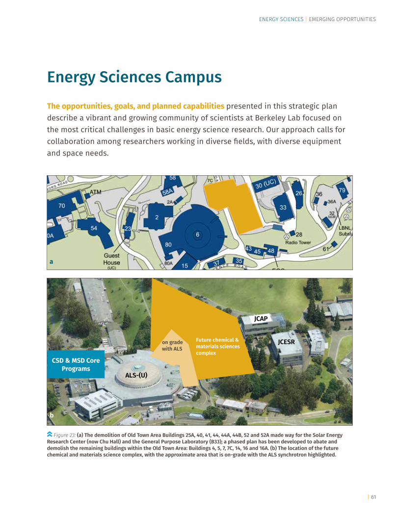
ALS-(U)
JCAP
JCESRFuture chemical & materials sciences complex
CSD & MSD Core Programs
| 61
ENERGY SCIENCES | EMERGING OPPORTUNITIES
Figure 23: (a) The demolition of Old Town Area Buildings 25A, 40, 41, 44, 44A, 44B, 52 and 52A made way for the Solar Energy Research Center (now Chu Hall) and the General Purpose Laboratory (B33); a phased plan has been developed to abate and demolish the remaining buildings within the Old Town Area: Buildings 4, 5, 7, 7C, 14, 16 and 16A. (b) The location of the future chemical and materials science complex, with the approximate area that is on-grade with the ALS synchrotron highlighted.
a
b
on grade with ALS
Energy Sciences CampusThe opportunities, goals, and planned capabilities presented in this strategic plan describe a vibrant and growing community of scientists at Berkeley Lab focused on the most critical challenges in basic energy science research. Our approach calls for collaboration among researchers working in diverse fields, with diverse equipment and space needs.
| 62
Colocation is a critical component to successful collaboration, and while the hilly terrain of the Berkeley Lab main site provides an inspiring work environment with stunning views, it can also serve as an impediment to collaborative relationships between colleagues whose labs and offices are in disparate corners of the Laboratory. Currently, the researchers of the Energy Sciences Area at Berkeley Lab are spread across some 27 buildings on the Hill campus site, and numerous others occupy lab and office space in additional buildings on the UC Berkeley campus. Creating additional high quality lab and office space that is clustered to encourage collaboration and a sense of community and shared purpose is a major long-term priority for basic energy sciences research at Berkeley Lab.
As part of Berkeley Lab’s long-range planning vision, the “Old Town” site, currently comprised of a number of World War II–era buildings slated for demolition (Figure 23a), has been reimagined as new campus for Energy Sciences. The availability of this centrally located and previously developed land provides us a crucial opportunity to carefully plan for the long-term future of collaborative basic energy “team science,” due to the site’s proximity to existing basic energy sciences research facilities, including the Advanced Light Source, Chu Hall (home of Berkeley Lab’s Joint Center for Artificial Photosynthesis research), the General Purpose Laboratory (home of the Joint Center for Energy Storage Research lab and office space), and MSD and CSD Core Program research in Building 2. The approximate extent of the available site, including the area that is on-grade with the ALS, is shown in Figure 23b.
The Chemical Observatory is the first idea to begin to take shape for this space, but other concepts that drive the construction of new buildings in this area will soon follow, capitalizing on the opportunity to design and build forward-looking research facilities that are ready to tackle the Grand Challenges of basic energy sciences, throughout the 21st Century.
The Chemical Observatory is a proposal for a revolutionary new type of research facility that combines the chemical specificity of soft X-rays with multiple simultaneous and coextensive observations, drawing upon a full suite of synthesis, characterization, and theory capabilities for a unified approach to understanding heterogeneous, complex, and dynamic systems and phenomena in basic energy science across a full range of relevant time and length scales. The facility is conceived a series of laboratory spaces constructed adjacent to the Advanced Light Source. Each laboratory will be equipped with custom instrumentation designed for multimodal observations in addition to customary laboratory equipment for targeted research areas, including chemical transformations, functional materials systems and devices, biological systems, and geosciences. The design and operation of this facility will hinge on a suite of mobile, interchangeable, and fully compatible instruments and components, along with custom software comprised of machine-learning algorithms to enable automated on-the-fly data analysis, workflow management, and design of experiments. The Chemical Observatory will enable a true paradigm shift for scientific observation in the 21st century, strengthening and sustaining the preeminent energy sciences research of the ALS and Berkeley Lab, and setting a new standard for the capabilities and implementation of DOE facilities.

| 63
ENERGY SCIENCES | EMERGING OPPORTUNITIES
Industry ConnectionsOur Area’s world-class expertise and instrumentation are uniquely suited to investigate a wide variety of materials and chemistry questions of interest to industrial researchers. Our User Facilities work with a growing number of industry scientists, whose work covers a diverse array of fields including: semiconductors, pharmaceuticals, energy storage, and photovoltaics. The questions that industry partners bring to our scientists can lead to new scientific discoveries, and enrich our knowledge and understanding of the phenomena and research areas relevant to emerging technologies.
Working closely with the world leaders in the semiconductor industry, MSD’s Center for X-Ray Optics (CXRO) is a one- of-a-kind facility with over 25 years of experience in the science and technology of short wavelength optical systems and techniques. CXRO’s capabilities include extreme ultraviolet (EUV) lithography, which enables the increasingly miniaturized circuit patterns required for the next generation of computer chips, and fabrication tools, processes, and materials for future semiconductor technologies. CXRO operates the world’s highest resolution EUV lithography tool and EUV mask-imaging microscope, and serves as the semiconductor industry’s premier center for advanced research into the future of chip manufacturing. CXRO is working to strengthen LBNL and MSD’s connections with the semiconductor industry and continues to play a key role in the innovation of future semiconductor solutions.
Part of our Area’s long-term strategic focus is to look for ways to strengthen our ties with applied research in topics that align with our expertise and capabilities. We are building collaborative partnerships with researchers in the Energy Technologies Area at Berkeley Lab, in areas such as fuel cells, batteries, and solar fuels production. Through JCAP and JCESR, our Energy Innovation Hubs whose missions include industry engagement, we are bringing in industrial partners to work on shared interests and common goals. Through these and other activities, we plan to increase our connections to industry research, and explore opportunities for mutually beneficial partnerships and projects.

| 64
Production credits:
Energy Sciences Area Donald J. DePaolo, Associate Laboratory Director
Editor: Melissa Summers, Energy Sciences Area Office
Photography: Roy Kaltschmidt, Public Affairs Department
Copywriting and editing: Lynn Yarris and Theresa Duque, Public Affairs Department, and Krys Aviña, Energy Sciences Area Office
Layout and design: Public Affairs Creative Services
Content provided by the following organizations: Materials Sciences DivisionChemical Sciences DivisionAdvanced Light SourceMolecular FoundryJoint Center for Artificial PhotosynthesisJoint Center for Energy Storage ResearchCenter for Nanoscale Controls on Geologic CO2The Materials ProjectCenter for Advanced Mathematics for Energy Research Applications
Energy Sciences Area | Lawrence Berkeley National Laboratory | One Cyclotron Road | Mail Stop 50B-4230 | Berkeley, CA 94720
From left to right, top to bottom:
JCAP scientist Ian Sharp aligns an ultrafast pulsed laser to probe the dynamics of photoexcited charge in systems used to convert solar energy to fuels.
Intern Christine Kang peforms peptoid robotics with postdoctoral fellow Alessia Battigelli in the Biological Nanostrurctures Facility of the Molecular Foundry.
Peng Chen at ALS beamline 10 and the spin-resolved chamber.
Intern Kirk Larsen works in the laser lab with mentor Daniel Slaughter of the Chemical Sciences Division.

16-ESA-2492
Related Documents