[AK4753] MS1311-E-04 2013/04 - 1 - GENERAL DESCRIPTION The AK4753 is a two input, four output audio CODEC with integrated digital signal processing. The outputs can be configured either as single-ended or differential. An internal PLL allows the chip to run in master clock free mode. The digital signal processing block includes an ALC/limiter, 5 configurable biquads for EQ, volume control, and 4 th -order filters for each output channel to enable a variety of configurations. Wide dynamic range is achieved with 96dB S/N for the ADC, and 103dB S/N for the DAC’s. A two-input 8-bit SAR ADC is integrated for processing of external potentiometers, supporting volume and bass control functions. A small external EEP-ROM is used to store the coefficient values for the DSP blocks. The AK4753 is controlled by an I 2 C control interface. FEATURES Digital audio input interface − Data format: MSB-first, two’s complement − 16, 20, or 24-bits, I2S, MSB justified, LSB justified, or DSP mode − Audio sampling rates: 8kHz to 48kHz Analog audio input − Single-ended input stereo 24-bit audio ADC − S/N: 96dB S/(N+D): 85dB − Digital high-pass filter for DC-offset correction Analog audio output − Four-channel 24-bit audio DAC − Single-ended or differential output − S/N: 103dB S/(N+D): 88dB 8-bit SAR ADC with two input selector Digital mixer for balancing inputs Digital signal processing block: DSP1, DSP2 independently − Configurable ALC / limiter function − Volume control: 0dB to -127dB, 0.5dB steps, mute − Pre-gain setting: 0dB, +6dB, +12dB, +18dB − Post-gain setting: 0dB, +3.5dB, +6dB, +8dB − Five programmable biquads for EQ − 4 th -order high-pass filter or low-pass filter Integrated PLL for master clock-free operation PLL − Input frequency: 24.576MHz, 24MHz, 22.5792MHz, 12.288MHz, 12MHz, and 11.2896MHz (XTI/MCKI pin) 1fs (LRCK pin), 32fs or 64fs (BICK pin) − Input level: CMOS or AC-coupled (XTI/MCKI pin) Master clock input: 256fs, 512fs, 1024fs μP I/F: I 2 C bus-slave (400kHz Fast-mode) EEP-ROM control I/F: I 2 C bus-master (400kHz Fast-mode) Ta = -30 ~ +85°C Power supply: Analog (AVDD): 3.0 ~ 3.6V (typ 3.3V) Digital (DVDD: 3.0 ~ 3.6V (typ 3.3V) Package: 32 pin QFN (4 x 4 mm, 0.4mm pitch) 2-in, 4-out CODEC with DSP Functions AK4753

Welcome message from author
This document is posted to help you gain knowledge. Please leave a comment to let me know what you think about it! Share it to your friends and learn new things together.
Transcript

[AK4753]
MS1311-E-04 2013/04 - 1 -
GENERAL DESCRIPTION The AK4753 is a two input, four output audio CODEC with integrated digital signal processing. The outputs can be configured either as single-ended or differential. An internal PLL allows the chip to run in master clock free mode. The digital signal processing block includes an ALC/limiter, 5 configurable biquads for EQ, volume control, and 4th-order filters for each output channel to enable a variety of configurations. Wide dynamic range is achieved with 96dB S/N for the ADC, and 103dB S/N for the DAC’s. A two-input 8-bit SAR ADC is integrated for processing of external potentiometers, supporting volume and bass control functions. A small external EEP-ROM is used to store the coefficient values for the DSP blocks. The AK4753 is controlled by an I2C control interface.
FEATURES
Digital audio input interface − Data format: MSB-first, two’s complement − 16, 20, or 24-bits, I2S, MSB justified, LSB justified, or DSP mode − Audio sampling rates: 8kHz to 48kHz
Analog audio input − Single-ended input stereo 24-bit audio ADC − S/N: 96dB S/(N+D): 85dB − Digital high-pass filter for DC-offset correction
Analog audio output − Four-channel 24-bit audio DAC − Single-ended or differential output − S/N: 103dB S/(N+D): 88dB
8-bit SAR ADC with two input selector Digital mixer for balancing inputs Digital signal processing block: DSP1, DSP2 independently
− Configurable ALC / limiter function − Volume control: 0dB to -127dB, 0.5dB steps, mute − Pre-gain setting: 0dB, +6dB, +12dB, +18dB − Post-gain setting: 0dB, +3.5dB, +6dB, +8dB − Five programmable biquads for EQ − 4th-order high-pass filter or low-pass filter
Integrated PLL for master clock-free operation PLL
− Input frequency: 24.576MHz, 24MHz, 22.5792MHz, 12.288MHz, 12MHz, and 11.2896MHz (XTI/MCKI pin) 1fs (LRCK pin), 32fs or 64fs (BICK pin)
− Input level: CMOS or AC-coupled (XTI/MCKI pin) Master clock input: 256fs, 512fs, 1024fs μP I/F: I2C bus-slave (400kHz Fast-mode) EEP-ROM control I/F: I2C bus-master (400kHz Fast-mode) Ta = -30 ~ +85°C Power supply:
Analog (AVDD): 3.0 ~ 3.6V (typ 3.3V) Digital (DVDD: 3.0 ~ 3.6V (typ 3.3V)
Package: 32 pin QFN (4 x 4 mm, 0.4mm pitch)
2-in, 4-out CODEC with DSP FunctionsAK4753
[AK4753]
MS1311-E-04 2013/04 - 2 -
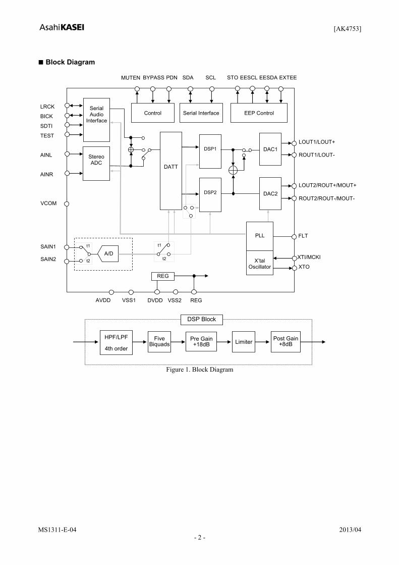
Block Diagram
LRCK
BICK
SDTI
AINL
AINR
Serial Audio
Interface
Stereo ADC
DSP1
Serial Interface
SCLSDA PDN
TEST
BYPASS
DVDD VSS2AVDD VSS1
VCOM
DATT
DSP2
Control
EEP Control
EESCL EESDA EXTEE
A/D SAIN1
SAIN2
LOUT1/LOUT+
DAC1ROUT1/LOUT-
LOUT2/ROUT+/MOUT+
ROUT2/ROUT-/MOUT-
DAC2
FLT
X’tal
Oscillator
XTI/MCKI
XTO
PLL
REG
REG
t1
t2
t1
t2
MUTEN STO
HPF/LPF
4th order
Pre Gain+18dB LimiterFive
Biquads
Post Gain +8dB
DSP Block
Figure 1. Block Diagram
[AK4753]
MS1311-E-04 2013/04 - 3 -
Ordering Guide
AK4753EN −30 ∼ +85°C 32 pin QFN (4 x 4 mm, 0.4mm pitch) AKD4753 Evaluation Board for AK4753
Pin Layout
NC
XTO
XTI/MCKI
DVDD
VSS2
REG
BYPASS
NC
BIC
K
LRC
K
SD
TI
STO
MU
TEN
SC
L
SD
A
EES
CL
VCO
M
LOU
T2/R
OU
T+/M
OU
T+
RO
UT2
/RO
UT-
/MO
UT-
RO
UT1
/LO
UT-
LOU
T1/L
OU
T+
AVD
D
VSS
1
AIN
L
EESDA
EXTEE
PDN
FLT
TEST
SAIN1
SAIN2
AINR
AK4753ENTop View
25
26
27
28
29
30
31
32
24
23
22
1
16
15
14
13
12
11
10
9
21
20
19
2 3 4 5 6 7 8
18
17

[AK4753]
MS1311-E-04 2013/04 - 4 -
PIN/FUNCTION No. Pin Name I/O Function
1 VCOM O Common voltage output pin This pin must be connected to VSS1 with the capacitors of 2.2μF capacitor in series.
LOUT2 O Lch Line-Amp Output 2 Pin Single-ended mode (SPC1-0 bits = “11”)
ROUT+ O Rch Line-Amp Positive Output Pin Differential mode (SPC1-0 bits = “00”, “01”) 2
MOUT+ O Mono Line-Amp Positive Output Pin Differential mode (SPC1-0 bits = “10”)
ROUT2 O Rch Line-Amp Output 2 Pin Single-ended mode (SPC1-0 bits = “11”)
ROUT− O Rch Line-Amp Negative Output Pin Differential mode (SPC1-0 bits = “00”, “01”) 3
MOUT− O Mono Line-Amp Negative Output Pin Differential mode (SPC1-0 bits = “10”)
ROUT1 O Rch Line-Amp Output 1 Pin Single-ended mode (SPC1-0 bits = “10”, “11”) 4
LOUT− O Lch Line-Amp Negative Output Pin Differential mode (SPC1-0 bits = “00”, “01”)
LOUT1 O Lch Line-Amp Output 1 Pin Single-ended mode (SPC1-0 bits = “10”, “11”) 5
LOUT+ O Lch Line-Amp Positive Output Pin Differential mode (SPC1-0 bits = “00”, “01”)
6 AVDD - Analog Power Supply Pin, 3.0V ~ 3.6V 7 VSS1 - Ground 1 Pin 8 AINL I L channel Analog Input Pin 9 AINR I R channel Analog Input Pin
10 SAIN2 I 8-bit SAR ADC Analog Input 2 Pin 11 SAIN1 I 8-bit SAR ADC Analog Input 1 Pin
12 TEST I TEST Input pin This pin must be connected to VSS2.
13 FLT O PLL Loop Filter Pin This pin must be connected to VSS1 with one resistor and one capacitor in series.
14 PDN I Power Down Pin
When “L”, the AK4753 is in power-down mode and is held in reset. The AK4753 must be always reset upon power-up.
15 EXTEE I EEP-ROM Enable Pin
“H”: EEP-ROM download mode “L”: Serial control mode
16 EESDA I/O EEP-ROM Control Data Input/Output Pin 17 EESCL O EEP-ROM Control Data Clock Output Pin 18 SDA I/O Control Data Input/Output Pin 19 SCL I Control Data Clock Input Pin
20 MUTEN O Mute Control Output Pin.
“H”: Normal Operation “L”: Mute
21 STO O EEP-ROM Status Output Pin
“H”: Read error “L”: No error
22 SDTI I Audio Serial Data Input Pin 23 LRCK I/O Input/Output Channel Clock Pin 24 BICK I/O Audio Serial Data Clock Pin
25 NC - No Connect Pin No internal bonding. This pin must be connected to VSS2.

[AK4753]
MS1311-E-04 2013/04 - 5 -
No. Pin Name I/O Function 26 XTO O X’tal Clock Output Pin
XTI I X’tal / External Clock Input Pin 27 MCKI I External Master Clock Input Pin 28 DVDD - Digital Power Supply Pin, 3.0V ~ 3.6V 29 VSS2 - Ground 2 Pin
30 REG O Regulator Ripple Filter Pin This pin must be connected to VSS2 with 2.2μF capacitor in series.
31 BYPASS I Bypass Control Input Pin
“H”: DSP Bypass mode “L”: Normal Operation
32 NC - No Connect Pin No internal bonding. This pin must be connected to VSS2.
Note 1. All input pins except analog input pins (AINL, AINR, SAIN1, SAIN2) must not be left floating. Handling of Unused Pin The unused I/O pins must be processed appropriately as below. Classification Pin Name Setting
Analog AINL, AINR, SAIN1, SAIN2, FLT, LOUT1/LOUT+, ROUT1/LOUT-, LOUT2/ROUT+/MOUT+, ROUT2/ROUT-/MOUT-
Open
XTO, SDA, EESDA, EESCL, MUTEN, STO Open Digital LRCK, BICK, SDTI, XTI/MCKI, EXTEE, TEST, SCL These pins must be connected to VSS2.

[AK4753]
MS1311-E-04 2013/04 - 6 -
ABSOLUTE MAXIMUM RATINGS (All VSS pins =0V; Note 2) Parameter Symbol min max Unit Power Supplies: Analog
Digital AVDD DVDD
-0.3 -0.3
4.2 4.2
V V
Analog Input Voltage (Note 3) VINA1 -0.3 AVDD+0.3 V Digital Input Voltage (Note 4) VIND -0.3 DVDD+0.3 V Input Current, Any Pin Except Supplies IIN -10 +10 mA Ambient Operating Temperature Ta -30 85 °C Storage Temperature Tstg -65 150 °C
Note 2. All voltage with respect to ground. All VSS pins must be connected to the common analog ground. Note 3. AINL pin, AINR pin, SAIN1 pin, SAIN2 pin. Note 4. BYPASS, PDN, EESDA, XTI/MCKI, BICK, LRCK, SDTI, SCL, SDA, TEST pins WARNING: Operation at or beyond these limits may result in permanent damage to the device. Normal operation is not
guaranteed at these extremes.
RECOMMENDED OPERATING CONDITIONS (All VSS pins =0V; Note 2) Parameter Symbol min typ max Unit Power Supplies (Note 5) Analog
Digital Difference
AVDD DVDD
|DVDD-AVDD|
3.0 3.0 -
3.3 3.3 0
3.6 3.6 0.3
V V V
Note 5. The power up sequence between AVDD and DVDD is not critical. Each power supplies should be powered up during the PDN pin = “L”. AVDD and DVDD must be the same voltage at the PDN pin = “H”. The PDN pin should be “H” after all power supplies are powered up. All power supplies should be powered on, only a part of these power supplies cannot be powered off. (Power off means power supplies equal to ground or power supplies are floating.) Do not turn off only the AK4753 under the condition that a surrounding device is powered on and the I2C bus is in use.
WARNING: AKM assumes no responsibility for the usage beyond the conditions in this datasheet.

CONFIDENTIAL [AK4753]
MS1311-E-04 2013/04 - 7 -
ANALOG CHARACTERISTICS (CODEC) (Ta=25°C; AVDD=DVDD=3.3V; VSS1=VSS2=0V; fs=44.1kHz; BICK=64fs; Signal Frequency=1kHz; 24-bit Data; Measurement Band Width =20Hz∼20kHz; unless otherwise specified) Parameter min typ max Unit DAC Analog Output Characteristics: DAC → LOUT1/ROUT1, LOUT2/ROUT2 pins,
Single-ended mode (SPC1-0 bits = “11”), HPF=LPF=EQ(5-BiQuads)=Limiter=OFF, DATT= 0dB, RL=5kΩ
Resolution - - 24 Bits S/(N+D) (0dBFS) 75 85 - dB DR (-60dBFS with A-weighted) 87 97 - dB S/N (A-weighted) 87 97 - dB Interchannel Isolation 80 95 - dB Interchannel Gain Mismatch - 0 0.5 dB Output Voltage AOUT=0.68 x AVDD 1.98 2.24 2.51 Vpp Load Resistance (AC load) 5 - - kΩ Load Capacitance - - 150 pF Power Supply Rejection Ratio (Note 6) - 50 - dB DAC Analog Output Characteristics: DAC → LOUT+/-, ROUT+/- pins,
Differential mode (SPC1-0 bits = “00”), HPF=LPF=EQ(5-BiQuads)=Limiter=OFF, DATT= 0dB, RL=5kΩ
S/(N+D) (0dBFS) 78 88 - dB DR (-60dBFS with A-weighted) 93 103 - dB S/N (A-weighted) 93 103 - dB Interchannel Isolation 95 110 - dB Interchannel Gain Mismatch - 0 0.5 dB Output Voltage AOUT=0.70 x AVDD ±2.08 ±2.31 ±2.54 Vpp Load Resistance (AC load) 5 - - kΩ Load Capacitance - - 150 pF Power Supply Rejection (Note 6) - 50 - dB ADC to DAC Characteristics: AINL/AINR pins → DAC → LOUT1/ROUT1, LOUT2/ROUT2 pins,
Single-ended mode (SPC1-0 bits = “11”), HPF=LPF=EQ(5-BiQuads)=Limiter=OFF, DATT= 0dB, RL=5kΩ
Input Voltage AIN=0.8xAVDD 2.38 2.64 2.90 Vpp Input Resistance 24 35 - kΩ S/(N+D) (-1dBFS) 73 84 - dB DR (-60dBFS with A-weighted) 83 94 - dB S/N (A-weighted) 83 94 - dB ADC to DAC Characteristics: AINL/AINR pins → DAC → LOUT+/-, ROUT+/- pins,
Differential mode (SPC1-0 bits = “00”, “01”), HPF=LPF=EQ(5-BiQuads)=Limiter=OFF, DATT= 0dB, RL=5kΩ
Input Voltage AIN=0.8xAVDD 2.38 2.64 2.90 Vpp Input Resistance 24 35 - kΩ S/(N+D) (-1dBFS) 74 85 - dB DR (-60dBFS with A-weighted) 85 96 - dB S/N (A-weighted) 85 96 - dB Note 6. PSRR is applied to AVDD and DVDD with 1kHz, 50mVpp.
CONFIDENTIAL [AK4753]
MS1311-E-04 2013/04 - 8 -
Parameter min typ max Unit Power Supplies All Circuit Power-up (PDN pin = “H”) (Note 7)
Differential Mode (SPC1-0 bits = “00”) AVDD - 5.8 8.7 mA DVDD - 4.2 6.3 mA
Single-ended Mode (SPC1-0 bits = “11”) AVDD - 9.0 13.5 mA
DVDD - 4.6 6.9 mA
Power-down (PDN pin = “L”) (Note 7) AVDD + DVDD - 1 10 µA Note 7. PLL Master Mode (MCKI=12MHz), PMAD=PMDIG=PMLO1=PMLO2=PMSAR=PMPLL bits = “1”. Note 8. All digital input pins are fixed to DVDD or VSS2.
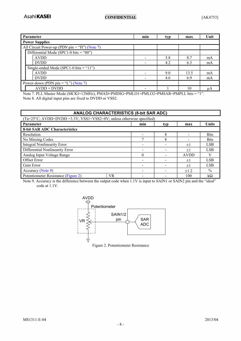
ANALOG CHARACTERISTICS (8-bit SAR ADC) (Ta=25°C; AVDD=DVDD =3.3V; VSS1=VSS2=0V; unless otherwise specified) Parameter min typ max Units 8-bit SAR ADC Characteristics Resolution - 8 - Bits No Missing Codes 7 8 - Bits Integral Nonlinearity Error - - ±1 LSB Differential Nonlinearity Error - - ±1 LSB Analog Input Voltage Range 0 - AVDD V Offset Error - - ±1 LSB Gain Error - - ±1 LSB Accuracy (Note 9) - - ±1.2 % Potentiometer Resistance (Figure 2) VR - - 100 kΩ Note 9. Accuracy is the difference between the output code when 1.1V is input to SAIN1 or SAIN2 pin and the “ideal”
code at 1.1V.
SAIN1/2pin
Potentiometer
VR SARADC
AVDD
Figure 2. Potentiometer Resistance

CONFIDENTIAL [AK4753]
MS1311-E-04 2013/04 - 9 -
FILTER CHARACTERISTICS (Ta =-30 ~ 85°C; AVDD=DVDD=3.0V ~ 3.6V; fs=44.1kHz; HPF=LPF=EQ(5-BiQuads)=Limiter=OFF) Parameter Symbol min typ max Unit ADC Digital Filter (Decimation LPF): Passband (Note 10) ±0.16dB PB 0 - 17.3 kHz −0.66dB - 19.4 - kHz −1.1dB - 19.9 - kHz −6.9dB - 22.1 - kHz Stopband SB 26.1 - - kHz Passband Ripple PR - - ±0.16 dB Stopband Attenuation SA 73 - - dB Group Delay (Note 11) GD - 15 - 1/fs Group Delay Distortion ΔGD - 0 - μs ADC Digital Filter (HPF): Frequency Response −3.0dB FR - 0.9 - Hz −0.1dB - 6.0 - Hz DAC Digital Filter: Passband (Note 12) ±0.05dB PB 0 - 20.0 kHz −6.0dB - 22.05 - kHz Stopband SB 24.1 - - kHz Passband Ripple PR - - ±0.05 dB Stopband Attenuation SA 53 - - dB Group Delay (Note 13) GD - 25 - 1/fs DAC Digital Filter (LPF) + SCF: Frequency Response: 0 ∼ 20.0kHz FR - ±0.4 - dB
Note 10. The passband and stopband frequencies scale with fs (system sampling rate). Each response refers to that of 1kHz.
Note 11. A calculating delay time which induced by digital filtering. This time is from the input of an analog signal to the setting of 24-bit data of both channels to the ADC output register.
Note 12. The passband and stopband frequencies scale with fs (system sampling rate). Each response refers to that of 1kHz.
Note 13. A calculating delay time which induced by digital filtering. This time is from setting the 24-bit data of both channels to input register to the output of analog signal.
DC CHARACTERISTICS (Ta=-30 ~ 85°C; AVDD=DVDD= 3.0V ~ 3.6V)
Parameter Symbol min typ max UnitHigh-Level Input Voltage VIH 70%DVDD - - V Low-Level Input Voltage VIL - - 30%DVDD V Input Voltage at AC Coupling (XTI/MCKI pin)
(Note 14) VAC 40%DVDD - - Vpp
High-Level Output Voltage (Note 15)(Iout = −100μA)
VOH
DVDD−0.4
-
-
V
Low-Level Output Voltage (Note 15) (Except SDA, EESDA, EESCL pins: Iout = 100μA) VOL - - 0.4 V
(SDA, EESDA, EESCL pins: Iout = 3mA) VOL - - 0.4 V Input Leakage Current Iin - - ±10 μA
Note 14. It is a case when AC coupling capacitor is connected to the XTI/MCKI pin. Note 15. Except XTO pin.
CONFIDENTIAL [AK4753]
MS1311-E-04 2013/04 - 10 -
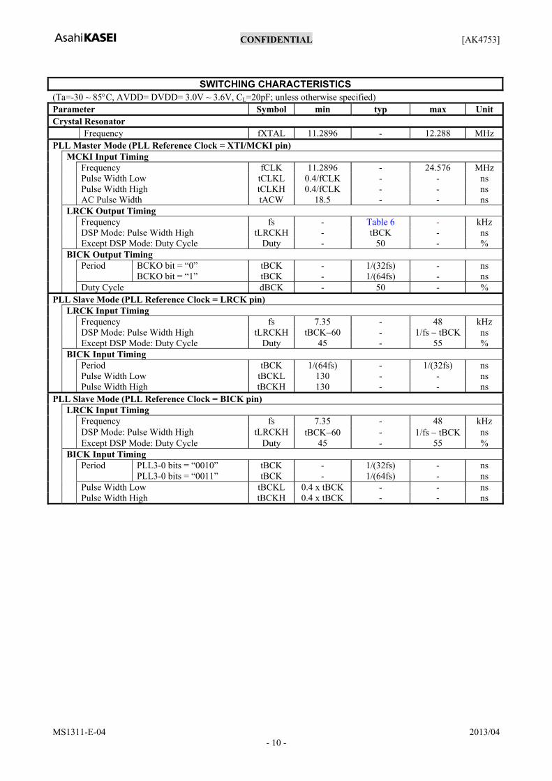
SWITCHING CHARACTERISTICS
(Ta=-30 ~ 85°C, AVDD= DVDD= 3.0V ~ 3.6V, CL=20pF; unless otherwise specified) Parameter Symbol min typ max Unit Crystal Resonator Frequency fXTAL 11.2896 - 12.288 MHz PLL Master Mode (PLL Reference Clock = XTI/MCKI pin) MCKI Input Timing Frequency fCLK 11.2896 - 24.576 MHz Pulse Width Low tCLKL 0.4/fCLK - - ns Pulse Width High tCLKH 0.4/fCLK - - ns AC Pulse Width tACW 18.5 - - ns LRCK Output Timing Frequency fs - Table 6 - kHz DSP Mode: Pulse Width High tLRCKH - tBCK - ns Except DSP Mode: Duty Cycle Duty - 50 - % BICK Output Timing Period BCKO bit = “0” tBCK - 1/(32fs) - ns BCKO bit = “1” tBCK - 1/(64fs) - ns Duty Cycle dBCK - 50 - % PLL Slave Mode (PLL Reference Clock = LRCK pin) LRCK Input Timing Frequency fs 7.35 - 48 kHz DSP Mode: Pulse Width High tLRCKH tBCK−60 - 1/fs − tBCK ns Except DSP Mode: Duty Cycle Duty 45 - 55 % BICK Input Timing Period tBCK 1/(64fs) - 1/(32fs) ns Pulse Width Low tBCKL 130 - - ns Pulse Width High tBCKH 130 - - ns PLL Slave Mode (PLL Reference Clock = BICK pin) LRCK Input Timing Frequency fs 7.35 - 48 kHz DSP Mode: Pulse Width High tLRCKH tBCK−60 - 1/fs − tBCK ns Except DSP Mode: Duty Cycle Duty 45 - 55 % BICK Input Timing Period PLL3-0 bits = “0010” tBCK - 1/(32fs) - ns PLL3-0 bits = “0011” tBCK - 1/(64fs) - ns Pulse Width Low tBCKL 0.4 x tBCK - - ns Pulse Width High tBCKH 0.4 x tBCK - - ns
CONFIDENTIAL [AK4753]
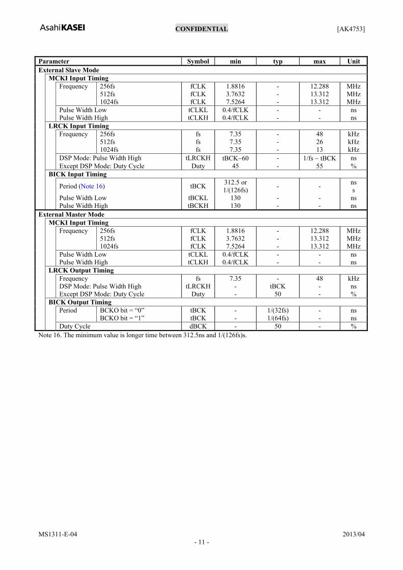
MS1311-E-04 2013/04 - 11 -
Parameter Symbol min typ max Unit External Slave Mode MCKI Input Timing Frequency 256fs fCLK 1.8816 - 12.288 MHz 512fs fCLK 3.7632 - 13.312 MHz 1024fs fCLK 7.5264 - 13.312 MHz Pulse Width Low tCLKL 0.4/fCLK - - ns Pulse Width High tCLKH 0.4/fCLK - - ns LRCK Input Timing Frequency 256fs fs 7.35 - 48 kHz 512fs fs 7.35 - 26 kHz 1024fs fs 7.35 - 13 kHz DSP Mode: Pulse Width High tLRCKH tBCK−60 - 1/fs − tBCK ns Except DSP Mode: Duty Cycle Duty 45 - 55 % BICK Input Timing
Period (Note 16) tBCK 312.5 or 1/(126fs) - - ns
s Pulse Width Low tBCKL 130 - - ns Pulse Width High tBCKH 130 - - ns External Master Mode MCKI Input Timing Frequency 256fs fCLK 1.8816 - 12.288 MHz 512fs fCLK 3.7632 - 13.312 MHz 1024fs fCLK 7.5264 - 13.312 MHz Pulse Width Low tCLKL 0.4/fCLK - - ns Pulse Width High tCLKH 0.4/fCLK - - ns LRCK Output Timing Frequency fs 7.35 - 48 kHz DSP Mode: Pulse Width High tLRCKH - tBCK - ns Except DSP Mode: Duty Cycle Duty - 50 - % BICK Output Timing Period BCKO bit = “0” tBCK - 1/(32fs) - ns BCKO bit = “1” tBCK - 1/(64fs) - ns Duty Cycle dBCK - 50 - % Note 16. The minimum value is longer time between 312.5ns and 1/(126fs)s.
CONFIDENTIAL [AK4753]
MS1311-E-04 2013/04 - 12 -
Parameter Symbol min typ max Unit
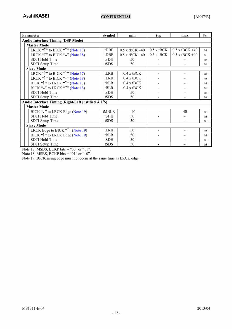
Audio Interface Timing (DSP Mode) Master Mode LRCK “↑” to BICK “↑” (Note 17) tDBF 0.5 x tBCK −40 0.5 x tBCK 0.5 x tBCK +40 ns LRCK “↑” to BICK “↓” (Note 18) tDBF 0.5 x tBCK −40 0.5 x tBCK 0.5 x tBCK +40 ns SDTI Hold Time tSDH 50 - - ns SDTI Setup Time tSDS 50 - - ns Slave Mode LRCK “↑” to BICK “↑” (Note 17) tLRB 0.4 x tBCK - - ns LRCK “↑” to BICK “↓” (Note 18) tLRB 0.4 x tBCK - - ns BICK “↑” to LRCK “↑” (Note 17) tBLR 0.4 x tBCK - - ns BICK “↓” to LRCK “↑” (Note 18) tBLR 0.4 x tBCK - - ns SDTI Hold Time tSDH 50 - - ns SDTI Setup Time tSDS 50 - - ns Audio Interface Timing (Right/Left justified & I2S) Master Mode BICK “↓” to LRCK Edge (Note 19) tMBLR −40 - 40 ns SDTI Hold Time tSDH 50 - - ns SDTI Setup Time tSDS 50 - - ns Slave Mode LRCK Edge to BICK “↑” (Note 19) tLRB 50 - - ns BICK “↑” to LRCK Edge (Note 19) tBLR 50 - - ns SDTI Hold Time tSDH 50 - - ns SDTI Setup Time tSDS 50 - - ns Note 17. MSBS, BCKP bits = “00” or “11”. Note 18. MSBS, BCKP bits = “01” or “10”. Note 19. BICK rising edge must not occur at the same time as LRCK edge.
CONFIDENTIAL [AK4753]
MS1311-E-04 2013/04 - 13 -
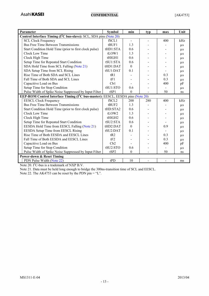
Parameter Symbol min typ max Unit Control Interface Timing (I2C bus-slave): SCL, SDA pins (Note 20) SCL Clock Frequency fSCL1 - - 400 kHz Bus Free Time Between Transmissions tBUF1 1.3 - - μs Start Condition Hold Time (prior to first clock pulse) tHD1:STA 0.6 - - μs Clock Low Time tLOW1 1.3 - - μs Clock High Time tHIGH1 0.6 - - μs Setup Time for Repeated Start Condition tSU1:STA 0.6 - - μs SDA Hold Time from SCL Falling (Note 21) tHD1:DAT 0 - - μs SDA Setup Time from SCL Rising tSU1:DAT 0.1 - - μs Rise Time of Both SDA and SCL Lines tR1 - - 0.3 μs Fall Time of Both SDA and SCL Lines tF1 - - 0.3 μs Capacitive Load on Bus Cb1 - - 400 pF Setup Time for Stop Condition tSU1:STO 0.6 - - μs Pulse Width of Spike Noise Suppressed by Input Filter tSP1 0 - 50 ns EEP-ROM Control Interface Timing (I2C bus-master): EESCL, EESDA pins (Note 20) EESCL Clock Frequency fSCL2 200 280 400 kHz Bus Free Time Between Transmissions tBUF2 1.3 - - μs Start Condition Hold Time (prior to first clock pulse) tHD:STA2 0.6 - - μs Clock Low Time tLOW2 1.3 - - μs Clock High Time tHIGH2 0.6 - - μs Setup Time for Repeated Start Condition tSU2:STA 0.6 - - μs EESDA Hold Time from EESCL Falling (Note 21) tHD2:DAT 0 - 0.9 μs EESDA Setup Time from EESCL Rising tSU2:DAT 0.1 - - μs Rise Time of Both EESDA and EESCL Lines tR2 - - 0.3 μs Fall Time of Both EESDA and EESCL Lines tF2 - - 0.3 μs Capacitive Load on Bus Cb2 - - 400 pF Setup Time for Stop Condition tSU2:STO 0.6 - - μs Pulse Width of Spike Noise Suppressed by Input Filter tSP2 0 - 50 ns Power-down & Reset Timing PDN Pulse Width (Note 22) tPD 10 - - ms Note 20. I2C-bus is a trademark of NXP B.V. Note 21. Data must be held long enough to bridge the 300ns-transition time of SCL and EESCL. Note 22. The AK4753 can be reset by the PDN pin = “L”.
CONFIDENTIAL [AK4753]
MS1311-E-04 2013/04 - 14 -
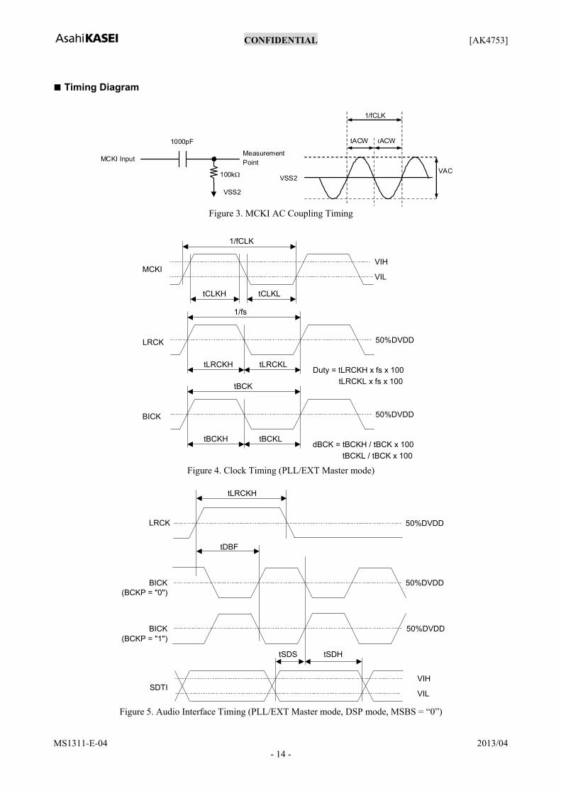
Timing Diagram
MCKI Input Measurement Point
VSS2
tACW tACW
VSS2
1/fCLK
1000pF
100kΩ VAC
Figure 3. MCKI AC Coupling Timing
LRCK
1/fCLK
MCKI
tCLKH tCLKL
VIH
VIL
1/fs
tLRCKH tLRCKL
50%DVDD
Duty = tLRCKH x fs x 100tLRCKL x fs x 100
BICK
tBCK
tBCKH tBCKL
50%DVDD
dBCK = tBCKH / tBCK x 100tBCKL / tBCK x 100
Figure 4. Clock Timing (PLL/EXT Master mode)
LRCK
BICK 50%DVDD
tDBF
50%DVDD
tLRCKH
BICK 50%DVDD
(BCKP = "0")
(BCKP = "1")
tSDS
SDTIVIL
tSDH
VIH
Figure 5. Audio Interface Timing (PLL/EXT Master mode, DSP mode, MSBS = “0”)
CONFIDENTIAL [AK4753]
MS1311-E-04 2013/04 - 15 -
LRCK
BICK 50%DVDD
tDBF
50%DVDD
tLRCKH
BICK 50%DVDD
(BCKP = "1")
(BCKP = "0")
tSDS
SDTIVIL
tSDH
VIH
Figure 6. Audio Interface Timing (PLL/EXT Master mode, DSP mode, MSBS = “1”)
LRCK 50%DVDD
BICK 50%DVDD
tSDS
SDTIVIL
tSDH
VIH
tMBLR
Figure 7. Audio Interface Timing (PLL/EXT Master mode, Except DSP mode)
1/fs
LRCKVIH
tLRCKH
VIL
tBCK
BICK
tBCKH tBCKL
VIH
VIL
tBLR
BICKVIH
VIL
(BCKP = "0")
(BCKP = "1")
Figure 8. Clock Timing (PLL Slave mode; PLL Reference Clock = LRCK or BICK pin, DSP mode, MSBS = “0”)

CONFIDENTIAL [AK4753]
MS1311-E-04 2013/04 - 16 -
1/fs
LRCKVIH
tLRCKH
VIL
tBCK
BICK
tBCKH tBCKL
VIH
VIL
tBLR
BICKVIH
VIL
(BCKP = "1")
(BCKP = "0") Figure 9. Clock Timing (PLL Slave mode; PLL Reference Clock = LRCK or BICK pin, DSP mode, MSBS = “1”)
LRCK
BICK
tSDS
SDTIVIL
tSDH
VIH
tLRB
tLRCKH
MSB
VIL
VIH
VIL
VIH
BICKVIL
VIH
(BCKP = "0")
(BCKP = "1")
Figure 10. Audio Interface Timing (PLL Slave mode, DSP mode; MSBS = “0”)
LRCK
BICK
tSDS
SDTIVIL
tSDH
VIH
tLRB
tLRCKH
MSB
VIL
VIH
VIL
VIH
BICKVIL
VIH
(BCKP = "1")
(BCKP = "0")
Figure 11. Audio Interface Timing (PLL Slave mode, DSP mode, MSBS = “1”)

CONFIDENTIAL [AK4753]
MS1311-E-04 2013/04 - 17 -
1/fCLK
MCKI
tCLKH tCLKL
VIH
VIL
1/fs
LRCKVIH
VIL
tBCK
BICK
tBCKH tBCKL
VIH
VIL
tLRCKH tLRCKL Duty = tLRCKH x fs x 100tLRCKL x fs x 100
Figure 12. Clock Timing (EXT Slave mode)
LRCKVIH
VIL
tBLR
BICKVIH
VIL
tLRB
tSDS
SDTIVIL
tSDH
VIH
Figure 13. Audio Interface Timing (PLL/EXT Slave mode, Except DSP mode)
StopStartStartStop
tHIGH
tHD:DAT
SDA
SCL
tBUFtLOW tR tF
tSU:DAT
VIH
VIL
tHD:STA tSU:STA
VIH
VIL
tSU:STO
tSP
Figure 14. I2C Bus Mode Timing
tPD
PDNVIL
Figure 15. Power Down & Reset Timing
[AK4753]
MS1311-E-04 2013/04 - 18 -
OPERATION OVERVIEW
Overview of AK4753 The AK4753 is an audio CODEC with integrated digital signal processors. It is easy to use since the two inputs 8-bit SAR ADC and EEP-ROM I/F are integrated. The SAR ADC has 2-channel input selector and the AD conversion is executed sequentially. The SAIN1 value is used to control the internal DATT. The SAIN2 value is used to control the gain of the EQ. When the analog input of the SAIN1/2 changes, the register value of the DATT/EQ is changed automatically. This external EEP-ROM is used to store the coefficient values for the DSP blocks, and the setting data. When the AK4753 is powered up, it reads the data in EEP-ROM at first, and maps these values into the internal registers. The following contents are stored in EEP-ROM. a. Fundamental function -Output Configuration Setting (Stereo mode, 2.1-channel mode or 4-channel mode)
-PLL mode setting: master or slave, PLL Reference Clock, Sampling Frequency -Audio Interface Format -DATT -Post-Gain and Pre-Gain setting for DSP1/2 -Limiter setting for DSP1/2 b. Coefficient data for DSP1/2 -Coefficient data of LPF/HPF -Coefficient data of Five Biquads
[AK4753]
MS1311-E-04 2013/04 - 19 -
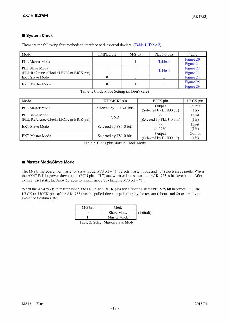
System Clock There are the following four methods to interface with external devices. (Table 1, Table 2) Mode PMPLL bit M/S bit PLL3-0 bits Figure
PLL Master Mode 1 1 Table 4 Figure 20 Figure 21
PLL Slave Mode (PLL Reference Clock: LRCK or BICK pin) 1 0 Table 4 Figure 22
Figure 23 EXT Slave Mode 0 0 x Figure 24
EXT Master Mode 0 1 x Figure 25 Figure 26
Table 1. Clock Mode Setting (x: Don’t care) Mode XTI/MCKI pin BICK pin LRCK pin
PLL Master Mode Selected by PLL3-0 bits Output (Selected by BCKO bit)
Output (1fs)
PLL Slave Mode (PLL Reference Clock: LRCK or BICK pin) GND Input
(Selected by PLL3-0 bits) Input (1fs)
EXT Slave Mode Selected by FS1-0 bits Input (≥ 32fs)
Input (1fs)
EXT Master Mode Selected by FS1-0 bits Output (Selected by BCKO bit)
Output (1fs)
Table 2. Clock pins state in Clock Mode Master Mode/Slave Mode The M/S bit selects either master or slave mode. M/S bit = “1” selects master mode and “0” selects slave mode. When the AK4753 is in power-down mode (PDN pin = “L”) and when exits reset state, the AK4753 is in slave mode. After exiting reset state, the AK4753 goes to master mode by changing M/S bit = “1”. When the AK4753 is in master mode, the LRCK and BICK pins are a floating state until M/S bit becomes “1”. The LRCK and BICK pins of the AK4753 must be pulled-down or pulled-up by the resistor (about 100kΩ) externally to avoid the floating state.
M/S bit Mode 0 Slave Mode (default)1 Master Mode
Table 3. Select Master/Slave Mode
[AK4753]
MS1311-E-04 2013/04 - 20 -
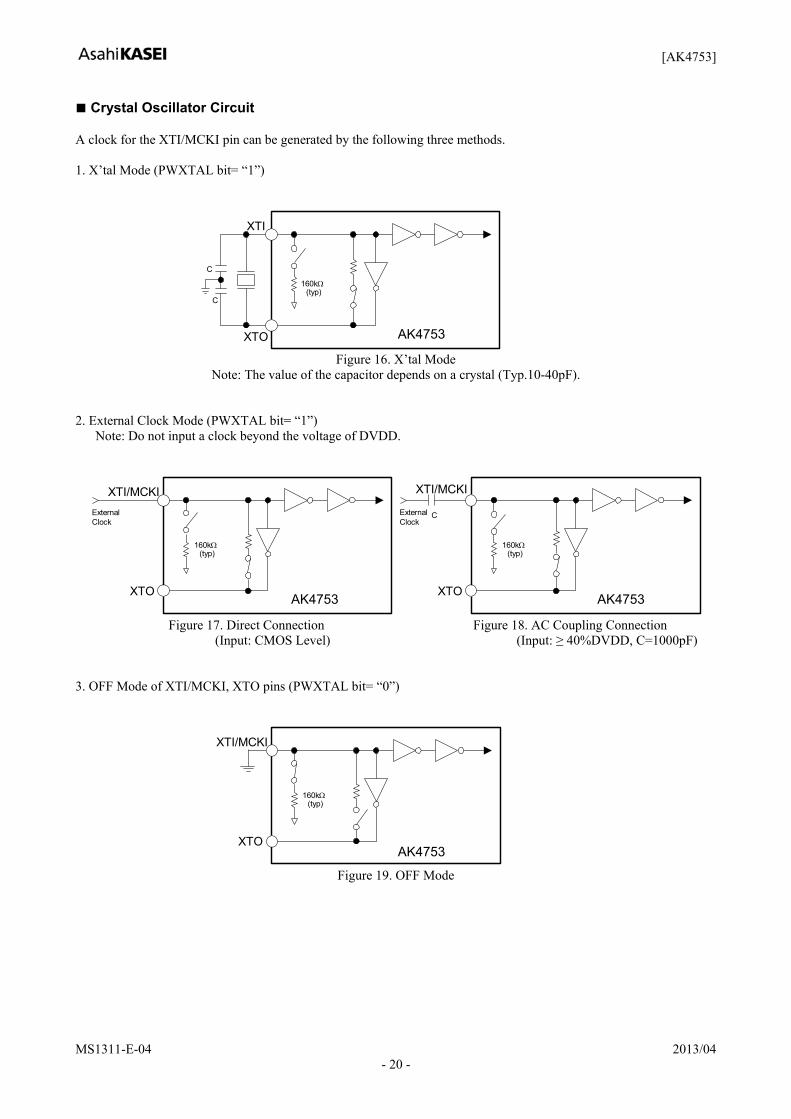
Crystal Oscillator Circuit A clock for the XTI/MCKI pin can be generated by the following three methods. 1. X’tal Mode (PWXTAL bit= “1”)
XTI
XTO AK4683
160kΩ
C
C(typ)
Figure 16. X’tal Mode
Note: The value of the capacitor depends on a crystal (Typ.10-40pF). 2. External Clock Mode (PWXTAL bit= “1”)
Note: Do not input a clock beyond the voltage of DVDD.
XTI/MCKI
XTOAK4683
ExternalClock
160kΩ(typ)
XTI/MCKI
XTOAK4683
ExternalClock
C
160kΩ(typ)
Figure 17. Direct Connection Figure 18. AC Coupling Connection
(Input: CMOS Level) (Input: ≥ 40%DVDD, C=1000pF)
3. OFF Mode of XTI/MCKI, XTO pins (PWXTAL bit= “0”)
XTI/MCKI
XTOAK4683
160kΩ(typ)
Figure 19. OFF Mode
AK4753
AK4753 AK4753
AK4753
[AK4753]
MS1311-E-04 2013/04 - 21 -
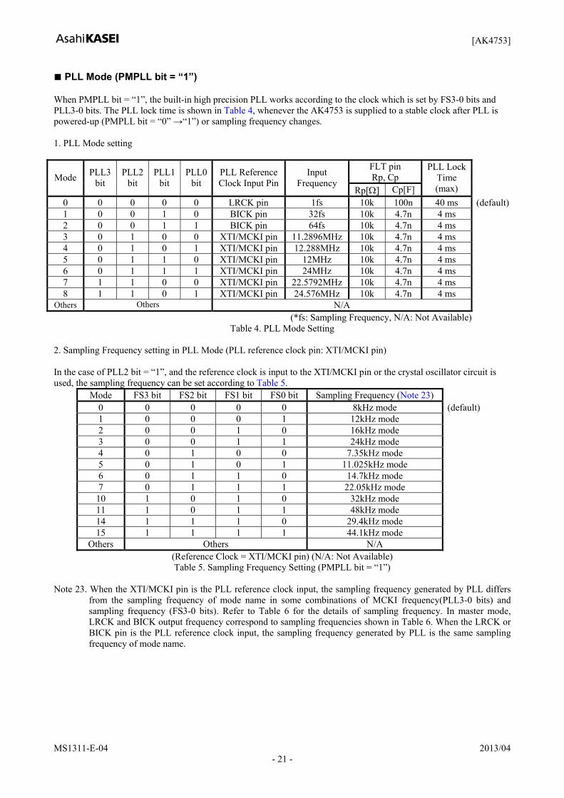
PLL Mode (PMPLL bit = “1”) When PMPLL bit = “1”, the built-in high precision PLL works according to the clock which is set by FS3-0 bits and PLL3-0 bits. The PLL lock time is shown in Table 4, whenever the AK4753 is supplied to a stable clock after PLL is powered-up (PMPLL bit = “0” →“1”) or sampling frequency changes. 1. PLL Mode setting
FLT pin Rp, Cp Mode PLL3
bit PLL2
bit PLL1
bit PLL0
bit PLL Reference Clock Input Pin
Input Frequency
Rp[Ω] Cp[F]
PLL Lock Time (max)
0 0 0 0 0 LRCK pin 1fs 10k 100n 40 ms (default)1 0 0 1 0 BICK pin 32fs 10k 4.7n 4 ms 2 0 0 1 1 BICK pin 64fs 10k 4.7n 4 ms 3 0 1 0 0 XTI/MCKI pin 11.2896MHz 10k 4.7n 4 ms 4 0 1 0 1 XTI/MCKI pin 12.288MHz 10k 4.7n 4 ms 5 0 1 1 0 XTI/MCKI pin 12MHz 10k 4.7n 4 ms 6 0 1 1 1 XTI/MCKI pin 24MHz 10k 4.7n 4 ms 7 1 1 0 0 XTI/MCKI pin 22.5792MHz 10k 4.7n 4 ms 8 1 1 0 1 XTI/MCKI pin 24.576MHz 10k 4.7n 4 ms
Others Others N/A (*fs: Sampling Frequency, N/A: Not Available)
Table 4. PLL Mode Setting 2. Sampling Frequency setting in PLL Mode (PLL reference clock pin: XTI/MCKI pin) In the case of PLL2 bit = “1”, and the reference clock is input to the XTI/MCKI pin or the crystal oscillator circuit is used, the sampling frequency can be set according to Table 5.
Mode FS3 bit FS2 bit FS1 bit FS0 bit Sampling Frequency (Note 23) 0 0 0 0 0 8kHz mode (default)1 0 0 0 1 12kHz mode 2 0 0 1 0 16kHz mode 3 0 0 1 1 24kHz mode 4 0 1 0 0 7.35kHz mode 5 0 1 0 1 11.025kHz mode 6 0 1 1 0 14.7kHz mode 7 0 1 1 1 22.05kHz mode
10 1 0 1 0 32kHz mode 11 1 0 1 1 48kHz mode 14 1 1 1 0 29.4kHz mode 15 1 1 1 1 44.1kHz mode
Others Others N/A (Reference Clock = XTI/MCKI pin) (N/A: Not Available) Table 5. Sampling Frequency Setting (PMPLL bit = “1”)
Note 23. When the XTI/MCKI pin is the PLL reference clock input, the sampling frequency generated by PLL differs
from the sampling frequency of mode name in some combinations of MCKI frequency(PLL3-0 bits) and sampling frequency (FS3-0 bits). Refer to Table 6 for the details of sampling frequency. In master mode, LRCK and BICK output frequency correspond to sampling frequencies shown in Table 6. When the LRCK or BICK pin is the PLL reference clock input, the sampling frequency generated by PLL is the same sampling frequency of mode name.

[AK4753]
MS1311-E-04 2013/04 - 22 -
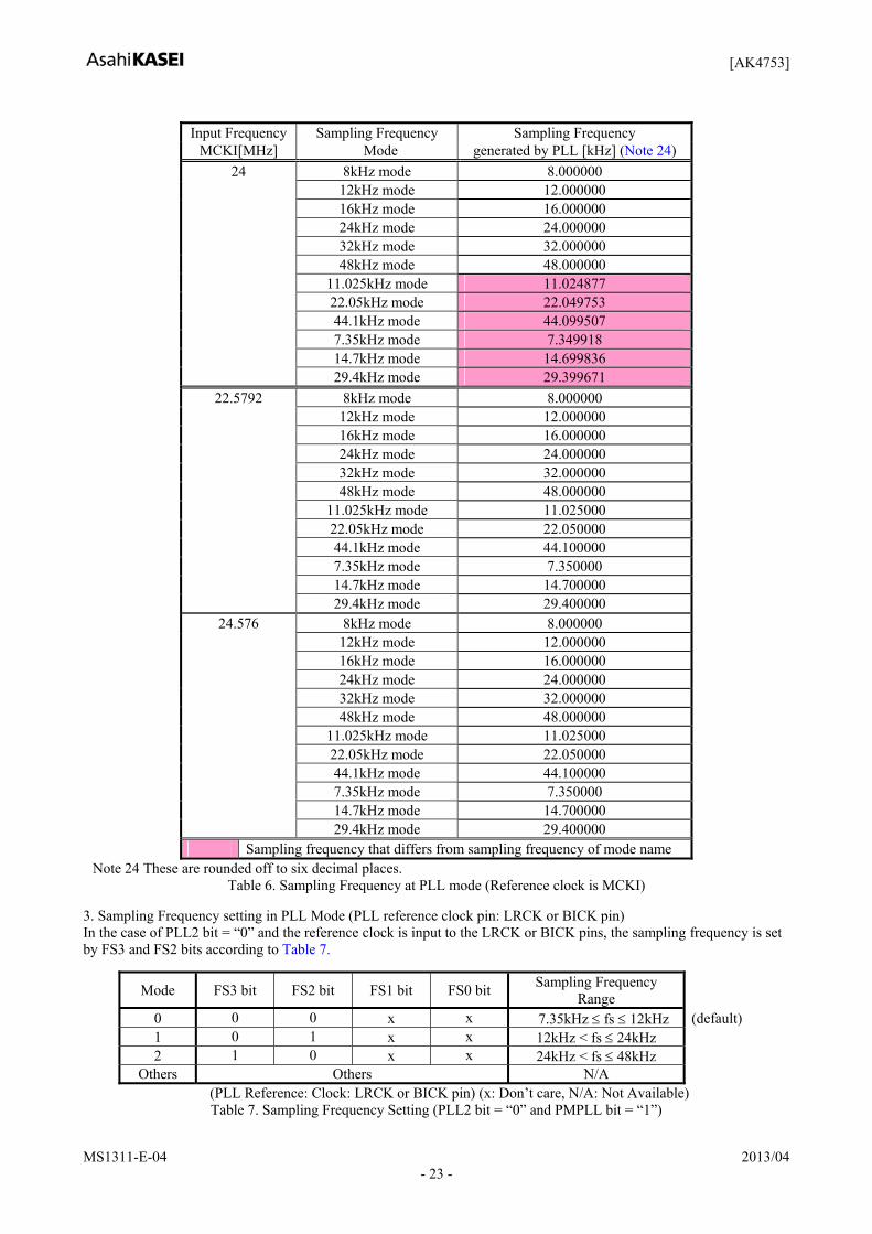
Input Frequency Sampling Frequency Sampling Frequency
MCKI[MHz] Mode generated by PLL [kHz] (Note 24) 11.2896 8kHz mode 8.000000
12kHz mode 12.000000 16kHz mode 16.000000 24kHz mode 24.000000 32kHz mode 32.000000 48kHz mode 48.000000 11.025kHz mode 11.025000 22.05kHz mode 22.050000 44.1kHz mode 44.100000 7.35kHz mode 7.350000 14.7kHz mode 14.700000 29.4kHz mode 29.400000
12.288 8kHz mode 8.000000 12kHz mode 12.000000 16kHz mode 16.000000 24kHz mode 24.000000 32kHz mode 32.000000 48kHz mode 48.000000 11.025kHz mode 11.025000 22.05kHz mode 22.050000 44.1kHz mode 44.100000 7.35kHz mode 7.350000 14.7kHz mode 14.700000 29.4kHz mode 29.400000
12 8kHz mode 8.000000 12kHz mode 12.000000 16kHz mode 16.000000 24kHz mode 24.000000 32kHz mode 32.000000 48kHz mode 48.000000 11.025kHz mode 11.024877 22.05kHz mode 22.049753 44.1kHz mode 44.099507 7.35kHz mode 7.349918 14.7kHz mode 14.699836 29.4kHz mode 29.399671
Sampling frequency that differs from sampling frequency of mode name Note 24. These are rounded off to six decimal places.
Table 6. Sampling Frequency at PLL mode (Reference clock is MCKI)
[AK4753]
MS1311-E-04 2013/04 - 23 -
Input Frequency Sampling Frequency Sampling Frequency
MCKI[MHz] Mode generated by PLL [kHz] (Note 24) 24 8kHz mode 8.000000
12kHz mode 12.000000 16kHz mode 16.000000 24kHz mode 24.000000 32kHz mode 32.000000 48kHz mode 48.000000 11.025kHz mode 11.024877 22.05kHz mode 22.049753 44.1kHz mode 44.099507 7.35kHz mode 7.349918 14.7kHz mode 14.699836 29.4kHz mode 29.399671
22.5792 8kHz mode 8.000000 12kHz mode 12.000000 16kHz mode 16.000000 24kHz mode 24.000000 32kHz mode 32.000000 48kHz mode 48.000000 11.025kHz mode 11.025000 22.05kHz mode 22.050000 44.1kHz mode 44.100000 7.35kHz mode 7.350000 14.7kHz mode 14.700000 29.4kHz mode 29.400000
24.576 8kHz mode 8.000000 12kHz mode 12.000000 16kHz mode 16.000000 24kHz mode 24.000000 32kHz mode 32.000000 48kHz mode 48.000000 11.025kHz mode 11.025000 22.05kHz mode 22.050000 44.1kHz mode 44.100000 7.35kHz mode 7.350000 14.7kHz mode 14.700000 29.4kHz mode 29.400000
Sampling frequency that differs from sampling frequency of mode name Note 24 These are rounded off to six decimal places.
Table 6. Sampling Frequency at PLL mode (Reference clock is MCKI) 3. Sampling Frequency setting in PLL Mode (PLL reference clock pin: LRCK or BICK pin) In the case of PLL2 bit = “0” and the reference clock is input to the LRCK or BICK pins, the sampling frequency is set by FS3 and FS2 bits according to Table 7.
Mode FS3 bit FS2 bit FS1 bit FS0 bit Sampling Frequency Range
0 0 0 x x 7.35kHz ≤ fs ≤ 12kHz (default)1 0 1 x x 12kHz < fs ≤ 24kHz 2 1 0 x x 24kHz < fs ≤ 48kHz
Others Others N/A (PLL Reference: Clock: LRCK or BICK pin) (x: Don’t care, N/A: Not Available) Table 7. Sampling Frequency Setting (PLL2 bit = “0” and PMPLL bit = “1”)
[AK4753]
MS1311-E-04 2013/04 - 24 -
PLL Un-Lock 1. PLL Master Mode (PMPLL bit = “1”, M/S bit = “1”) In this mode, the BICK and LRCK pins go to “L” before the PLL goes to lock state after PMPLL bit = “0” →“1” (Table 8). After the PLL is locked, a first period of LRCK and BICK may be invalid clock, but these clocks return to normal state after a period of 1/fs. When sampling frequency is changed, the BICK and LRCK pins do not output irregular frequency clocks but go to “L” by setting PMPLL bit to “0”.
PLL State BICK pin LRCK pin PMPLL bit “0” “1” “L” Output “L” Output PLL Unlock (Except for the above) Not fixed Not fixed PLL Lock Table 9 1fs Output Table 8. Clock Operation at PLL Master Mode (PMPLL bit = “1”, M/S bit = “1”)
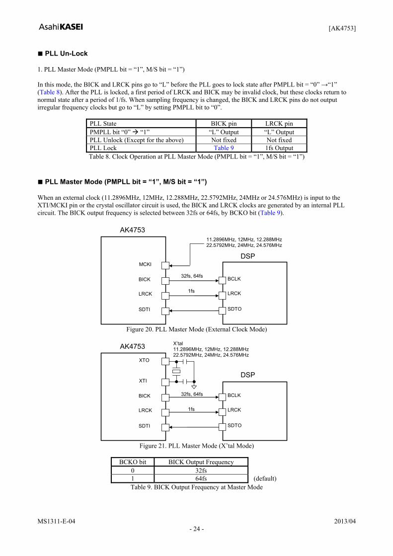
PLL Master Mode (PMPLL bit = “1”, M/S bit = “1”) When an external clock (11.2896MHz, 12MHz, 12.288MHz, 22.5792MHz, 24MHz or 24.576MHz) is input to the XTI/MCKI pin or the crystal oscillator circuit is used, the BICK and LRCK clocks are generated by an internal PLL circuit. The BICK output frequency is selected between 32fs or 64fs, by BCKO bit (Table 9).
AK4753
DSP
BICK
LRCK
SDTI
BCLK
LRCK
SDTO
MCKI
1fs
32fs, 64fs
11.2896MHz, 12MHz, 12.288MHz 22.5792MHz, 24MHz, 24.576MHz
Figure 20. PLL Master Mode (External Clock Mode)
AK4753
DSP
BICK
LRCK
SDTI
BCLK
LRCK
SDTO
XTI
1fs
32fs, 64fs
X’tal 11.2896MHz, 12MHz, 12.288MHz 22.5792MHz, 24MHz, 24.576MHz
XTO
Figure 21. PLL Master Mode (X’tal Mode)
BCKO bit BICK Output Frequency
0 32fs 1 64fs (default)Table 9. BICK Output Frequency at Master Mode
[AK4753]
MS1311-E-04 2013/04 - 25 -
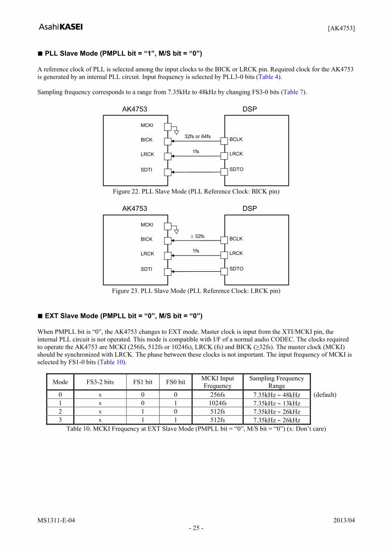
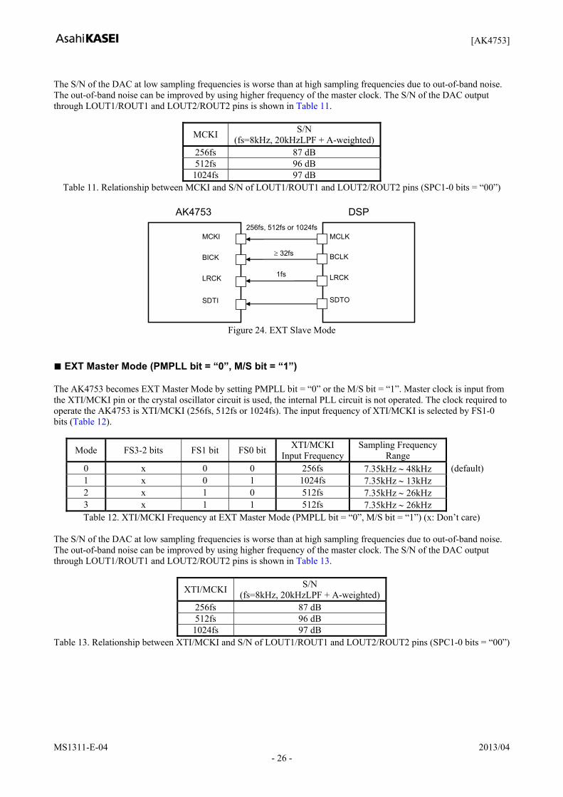
PLL Slave Mode (PMPLL bit = “1”, M/S bit = “0”) A reference clock of PLL is selected among the input clocks to the BICK or LRCK pin. Required clock for the AK4753 is generated by an internal PLL circuit. Input frequency is selected by PLL3-0 bits (Table 4). Sampling frequency corresponds to a range from 7.35kHz to 48kHz by changing FS3-0 bits (Table 7).
AK4753 DSP
MCKI
BICK
LRCK
SDTI
BCLK
LRCK
SDTO
1fs
32fs or 64fs
Figure 22. PLL Slave Mode (PLL Reference Clock: BICK pin)
AK4753 DSP
MCKI
BICK
LRCK
SDTI
BCLK
LRCK
SDTO
1fs
≥ 32fs
Figure 23. PLL Slave Mode (PLL Reference Clock: LRCK pin)
EXT Slave Mode (PMPLL bit = “0”, M/S bit = “0”) When PMPLL bit is “0”, the AK4753 changes to EXT mode. Master clock is input from the XTI/MCKI pin, the internal PLL circuit is not operated. This mode is compatible with I/F of a normal audio CODEC. The clocks required to operate the AK4753 are MCKI (256fs, 512fs or 1024fs), LRCK (fs) and BICK (≥32fs). The master clock (MCKI) should be synchronized with LRCK. The phase between these clocks is not important. The input frequency of MCKI is selected by FS1-0 bits (Table 10).
Mode FS3-2 bits FS1 bit FS0 bit MCKI Input Frequency
Sampling Frequency Range
0 x 0 0 256fs 7.35kHz ∼ 48kHz (default) 1 x 0 1 1024fs 7.35kHz ∼ 13kHz 2 x 1 0 512fs 7.35kHz ∼ 26kHz 3 x 1 1 512fs 7.35kHz ∼ 26kHz
Table 10. MCKI Frequency at EXT Slave Mode (PMPLL bit = “0”, M/S bit = “0”) (x: Don’t care)
[AK4753]
MS1311-E-04 2013/04 - 26 -
The S/N of the DAC at low sampling frequencies is worse than at high sampling frequencies due to out-of-band noise. The out-of-band noise can be improved by using higher frequency of the master clock. The S/N of the DAC output through LOUT1/ROUT1 and LOUT2/ROUT2 pins is shown in Table 11.
MCKI S/N (fs=8kHz, 20kHzLPF + A-weighted)
256fs 87 dB 512fs 96 dB
1024fs 97 dB Table 11. Relationship between MCKI and S/N of LOUT1/ROUT1 and LOUT2/ROUT2 pins (SPC1-0 bits = “00”)
AK4753 DSP
MCKI
BICK
LRCK
SDTI
BCLK
LRCK
SDTO
1fs
≥ 32fs
MCLK 256fs, 512fs or 1024fs
Figure 24. EXT Slave Mode
EXT Master Mode (PMPLL bit = “0”, M/S bit = “1”) The AK4753 becomes EXT Master Mode by setting PMPLL bit = “0” or the M/S bit = “1”. Master clock is input from the XTI/MCKI pin or the crystal oscillator circuit is used, the internal PLL circuit is not operated. The clock required to operate the AK4753 is XTI/MCKI (256fs, 512fs or 1024fs). The input frequency of XTI/MCKI is selected by FS1-0 bits (Table 12).
Mode FS3-2 bits FS1 bit FS0 bit XTI/MCKI Input Frequency
Sampling Frequency Range
0 x 0 0 256fs 7.35kHz ∼ 48kHz (default) 1 x 0 1 1024fs 7.35kHz ∼ 13kHz 2 x 1 0 512fs 7.35kHz ∼ 26kHz 3 x 1 1 512fs 7.35kHz ∼ 26kHz Table 12. XTI/MCKI Frequency at EXT Master Mode (PMPLL bit = “0”, M/S bit = “1”) (x: Don’t care)
The S/N of the DAC at low sampling frequencies is worse than at high sampling frequencies due to out-of-band noise. The out-of-band noise can be improved by using higher frequency of the master clock. The S/N of the DAC output through LOUT1/ROUT1 and LOUT2/ROUT2 pins is shown in Table 13.
XTI/MCKI S/N (fs=8kHz, 20kHzLPF + A-weighted)
256fs 87 dB 512fs 96 dB
1024fs 97 dB Table 13. Relationship between XTI/MCKI and S/N of LOUT1/ROUT1 and LOUT2/ROUT2 pins (SPC1-0 bits = “00”)

[AK4753]
MS1311-E-04 2013/04 - 27 -
AK4753 DSP
MCKI
BICK
LRCK
SDTI
BCLK
LRCK
SDTO
1fs
32fs or 64fs
MCLK 256fs, 512fs or 1024fs
Figure 25. EXT Master Mode (External Clock Mode)
AK4753
DSP
BICK
LRCK
SDTI
BCLK
LRCK
SDTO
XTI
1fs
32fs, 64fs
X’tal 256fs, 512fs or 1024fs
XTO
Figure 26. EXT Master Mode (X’tal Mode)
BCKO bit BICK Output Frequency 0 32fs 1 64fs (default)
Table 14. BICK Output Frequency at Master Mode
[AK4753]
MS1311-E-04 2013/04 - 28 -
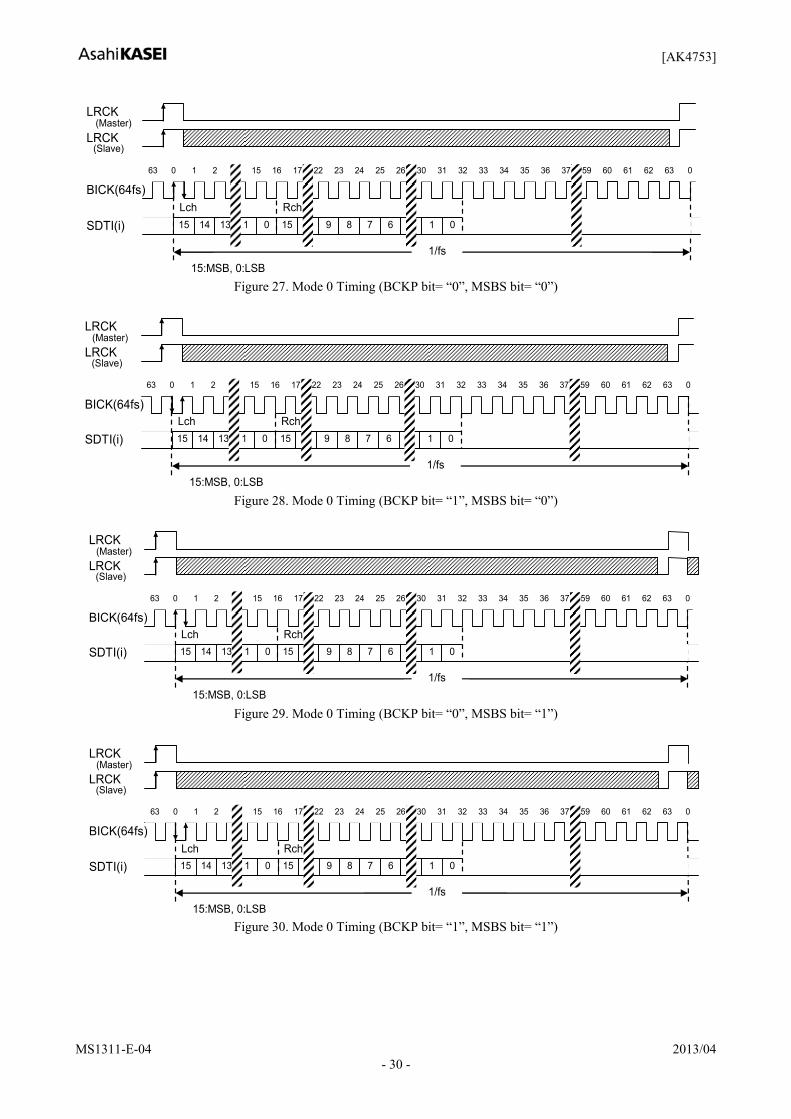
System Reset Upon power-up, the AK4753 must be reset by bringing the PDN pin = “L”. This ensures that all internal registers reset to their initial values. The PDN pin must be set to “L” at power-up. When PMADC bit is changed from “0” to “1”, the initialization cycle of ADC starts. The ADC outputs settle to data correspondent to the input signals after the end of initialization. The time from the input of analog signals to the output of analog signals including the initialization cycle of ADC is 1098/fs=25ms@fs=44.1kHz. Audio Interface Format Eight types of the data formats are available and are selected by setting the DIF2-0 bits (Table 15). In all modes, the serial data is MSB first, 2’s complement format. Audio interface formats can be used in both master mode and slave mode. LRCK and BICK are output from the AK4753 in master mode, but must be input to the AK4753 in slave mode.
Mode DIF2 bit
DIF1 bit
DIF0 bit SDTI LRCK BICK Figure
0 0 0 0 16-bit DSP Mode H/L ≥32fs Table 16 1 0 0 1 16-bit LSB justified H/L ≥32fs Figure 31 2 0 1 0 16/20/24-bit MSB justified H/L 32fs or ≥48fs Figure 33 3 0 1 1 16/20/24-bit I2S compatible L/H 32fs or ≥48fs Figure 34 (default)4 1 0 0 20-bit LSB justified H/L ≥40fs Figure 32 5 1 0 1 24-bit LSB justified H/L ≥48fs Figure 32 6 1 1 0 20-bit DSP Mode H/L ≥48fs Table 17 7 1 1 1 24-bit DSP Mode H/L ≥48fs Table 18
Table 15. Audio Interface Format In Mode 1/2/3/4/5, the SDTI is latched on the rising edge (“↑”) of BICK. In Modes 0/6/7 (DSP mode), the audio I/F timing is changed by BCKP and MSBS bits. When BCKP bit = “0”, the SDTI is latched on the falling edge (“↓”) of BICK. When BCKP bit = “1”, the SDTI is latched on the rising edge (“↑”) of BICK. MSBS bit can shift the position of the MSB data of SDTI to the position of the half cycle of the BICK.

[AK4753]
MS1311-E-04 2013/04 - 29 -
DIF2 DIF1 DIF0 MSBS BCKP Audio Interface Format Figure
0 0 MSB data of SDTI is latched on the falling edge (“↓”) of the first BICK after the rising edge (“↑”) of LRCK.
Figure 27 (default)
0 1 MSB data of SDTI is latched on the rising edge (“↑”) of the first BICK after the rising edge (“↑”) of LRCK.
Figure 28
1 0
MSB data of SDTI is latched on the falling edge (“↓”) of the first BICK after the falling edge (“↓”) of the first BICK after the rising edge (“↑”) of LRCK.
Figure 29
0 0 0
1 1 MSB data of SDTI is latched on the rising edge (“↑”) of the first BICK after the rising edge (“↑”) of the first BICK after the rising edge (“↑”) of LRCK.
Figure 30
Table 16. Audio Interface Format in Mode 0
DIF2 DIF1 DIF0 MSBS BCKP Audio Interface Format Figure
0 0 MSB data of SDTI is latched on the falling edge (“↓”) of the first BICK after the rising edge (“↑”) of LRCK.
Figure 35 (default)
0 1 MSB data of SDTI is latched on the rising edge (“↑”) of the first BICK after the rising edge (“↑”) of LRCK.
Figure 36
1 0
MSB data of SDTI is latched on the falling edge (“↓”) of the first BICK after the falling edge (“↓”) of the first BICK after the rising edge (“↑”) of LRCK.
Figure 37
1 1 0
1 1 MSB data of SDTI is latched on the rising edge (“↑”) of the first BICK after the rising edge (“↑”) of the first BICK after the rising edge (“↑”) of LRCK.
Figure 38
Table 17. Audio Interface Format in Mode 6
DIF2 DIF1 DIF0 MSBS BCKP Audio Interface Format Figure
0 0 MSB data of SDTI is latched on the falling edge (“↓”) of the first BICK after the rising edge (“↑”) of LRCK.
Figure 39 (default)
0 1 MSB data of SDTI is latched on the rising edge (“↑”) of the first BICK after the rising edge (“↑”) of LRCK.
Figure 40
1 0
MSB data of SDTI is latched on the falling edge (“↓”) of the first BICK after the falling edge (“↓”) of the first BICK after the rising edge (“↑”) of LRCK.
Figure 41
1 1 1
1 1 MSB data of SDTI is latched on the rising edge (“↑”) of the first BICK after the rising edge (“↑”) of the first BICK after the rising edge (“↑”) of LRCK.
Figure 42
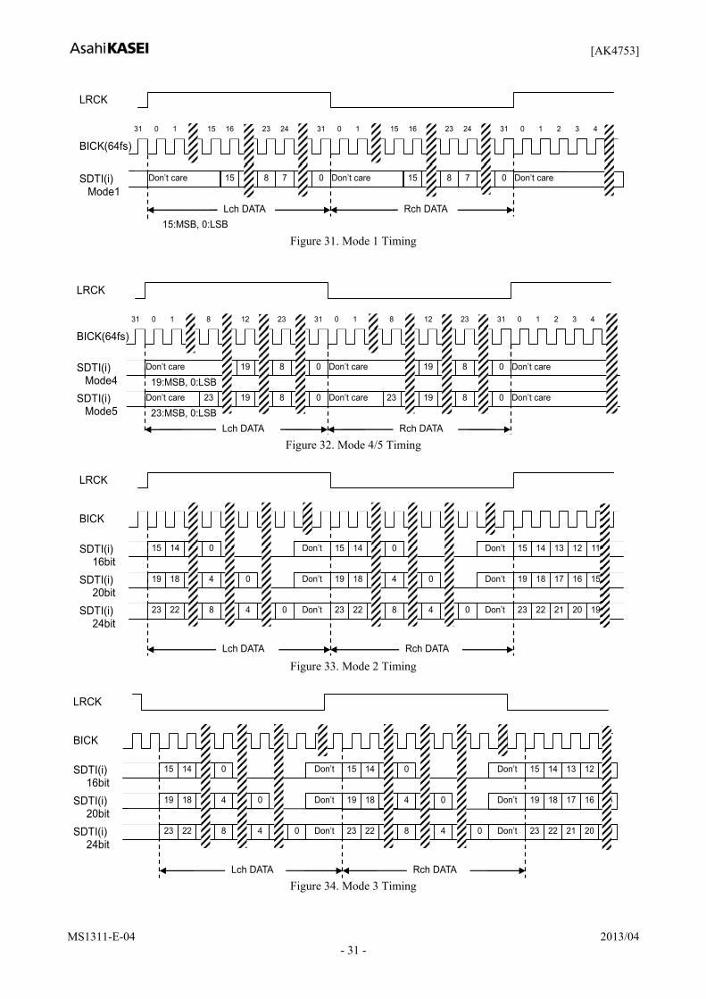
Table 18. Audio Interface Format in Mode 7
[AK4753]
MS1311-E-04 2013/04 - 30 -
LRCK (Master)
LRCK (Slave)
1/fs 15:MSB, 0:LSB
63 0 1 2 14 15 16 17 22 23 24 25 26 30 31 32 33 34 35 36 37
BICK(64fs)
SDTI(i) Lch Rch
59 60 61 62 63
15 14 13 1 0 15 9 8 7 6 1 0
0
Figure 27. Mode 0 Timing (BCKP bit= “0”, MSBS bit= “0”)
LRCK (Master)
LRCK (Slave)
1/fs 15:MSB, 0:LSB
63 0 1 2 14 15 16 17 22 23 24 25 26 30 31 32 33 34 35 36 37
BICK(64fs)
SDTI(i) Lch Rch
59 60 61 62 63
15 14 13 1 0 15 9 8 7 6 1 0
0
Figure 28. Mode 0 Timing (BCKP bit= “1”, MSBS bit= “0”)
1/fs 15:MSB, 0:LSB
63 0 1 2 14 15 16 17 22 23 24 25 26 30 31 32 33 34 35 36 37
BICK(64fs)
SDTI(i) Lch Rch
59 60 61 62 63
15 14 13 1 0 15 9 8 7 6 1 0
0
LRCK (Master)
LRCK (Slave)
Figure 29. Mode 0 Timing (BCKP bit= “0”, MSBS bit= “1”)
1/fs 15:MSB, 0:LSB
63 0 1 2 14 15 16 17 22 23 24 25 26 30 31 32 33 34 35 36 37
BICK(64fs)
SDTI(i) Lch Rch
59 60 61 62 63
15 14 13 1 0 15 9 8 7 6 1 0
0
LRCK (Master)
LRCK (Slave)
Figure 30. Mode 0 Timing (BCKP bit= “1”, MSBS bit= “1”)
[AK4753]
MS1311-E-04 2013/04 - 31 -
LRCK
31 0 1 15 16 23 24 31 0 1 15 16 23 24 31
BICK(64fs)
SDTI(i) Mode1
0 1 2 3 4
15 14 8 7 13 0 15 8 7 0
Don’t care Don’t care Don’t care
Lch DATA Rch DATA 15:MSB, 0:LSB
Figure 31. Mode 1 Timing
LRCK
31 0 1 8 12 23 31 0 1 8 12 23 31
BICK(64fs)
SDTI(i) Mode4 19:MSB, 0:LSB
0 1 2 3 4
19 8 0 19 8 1 0 19
5
23:MSB, 0:LSB
Don’t care Don’t care Don’t care
Lch DATA Rch DATA
SDTI(i) Mode5
23 19 20 8 0 23 19 8 1 0 22 21 20 19Don’t care Don’t care Don’t care
Figure 32. Mode 4/5 Timing
LRCK
BICK
SDTI(i) 16bit
14 0 Don’t 14 13 12 11
15 15
Lch DATA Rch DATA
SDTI(i) 20bit
18 4 20 0 Don’t 18 17 16 1519 19
SDTI(i) 24bit
22 8 4 20 0 Don’t 22 21 20 1923 23
14 0 Don’t 15
18 4 200 Don’t 19
22 8 4 20 0 Don’t 23
Figure 33. Mode 2 Timing
LRCK
BICK
SDTI(i) 16bit
14 0 Don’t 14 13 12 11
15 15
Lch DATA Rch DATA
SDTI(i) 20bit
18 4 20 0 Don’t 18 17 16 1519 19
SDTI(i) 24bit
22 8 4 20 0 Don’t 22 21 20 1923 23
14 0 Don’t 15
18 4 200 Don’t 19
22 8 4 20 0 Don’t 23
Figure 34. Mode 3 Timing

[AK4753]
MS1311-E-04 2013/04 - 32 -
LRCK (Master)
LRCK (Slave)
1/fs 19:MSB, 0:LSB
63 0 1 2 14 20 21 23 24 25 26 27 37 38 39 40 41 42 43 44 45
BICK(64fs)
SDTI(i) Lch
46 61 62 63
19 18 17 0 19 16 15 14 13 9 2 1 0
0
Rch
Figure 35. Mode 6 Timing (BCKP bit= “0”, MSBS bit= “0”)
LRCK (Master
)LRCK (Slave)
1/fs 19:MSB, 0:LSB
63 0 1 2 14 20 21 23 24 25 26 27 37 38 39 40 41 42 43 44 45
BICK(64fs)
SDTI(i) Lch
46 61 62 63
19 18 17 0 19 16 15 14 13 9 2 1
0
Rch 0
Figure 36. Mode 6 Timing (BCKP bit= “1”, MSBS bit= “0”)
LRCK (Master)
LRCK (Slave)
1/fs 19:MSB, 0:LSB
63 0 1 2 14 20 21 23 24 25 26 27 37 38 39 40 41 42 43 44 45
BICK(64fs)
SDTI(i) Lch
46 61 62 63
19 18 17 0 19 16 15 14 13 9 2 1
0
Rch 0
Figure 37. Mode 6 Timing (BCKP bit= “0”, MSBS bit= “1”)
LRCK (Master)
LRCK (Slave)
1/fs19:MSB, 0:LSB
63 0 1 2 14 20 21 23 24 25 26 27 37 38 39 40 41 42 43 44 45
BICK(64fs)
SDTI(i) Lch
46 61 62 63
19 18 17 20 19 16 15 14 13 9 2 1
0
Rch 0
Figure 38. Mode 6 Timing (BCKP bit= “1”, MSBS bit= “1”)
[AK4753]
MS1311-E-04 2013/04 - 33 -
LRCK (Master)
LRCK (Slave)
1/fs 23:MSB, 0:LSB
63 0 1 2 14 20 21 23 24 25 26 27 37 38 39 40 41 46 47 48 49
BICK(64fs)
SDTI(i)
50 61 62 63 0
23 22 21 4 3 0 23 22 21 1 10 9 8 7 2 1 Lch Rch
0
Figure 39. Mode 7 Timing (BCKP bit= “0”, MSBS bit= “0”)
LRCK (Master)
LRCK (Slave)
1/fs 23:MSB, 0:LSB
63 0 1 2 14 20 21 23 24 25 26 27 37 38 39 40 41 46 47 48 49
BICK(64fs)
SDTI(i)
50 61 62 63 0
23 22 21 4 3 0 23 22 21 1 10 9 8 7 2 1 Lch Rch
0
Figure 40. Mode 7 Timing (BCKP bit= “1”, MSBS bit= “0”)
LRCK (Master)
LRCK (Slave)
1/fs23:MSB, 0:LSB
63 0 1 2 14 20 21 23 24 25 26 27 37 38 39 40 41 46 47 48 49
BICK(64fs)
SDTI(i)
50 61 62 63 0
23 22 21 4 3 0 23 22 21 1 10 9 8 7 2 1 Lch Rch
0
Figure 41. Mode 7 Timing (BCKP bit= “0”, MSBS bit= “1”)
LRCK (Master)
LRCK (Slave)
1/fs 23:MSB, 0:LSB
63 0 1 2 14 20 21 23 24 25 26 27 37 38 39 40 41 46 47 48 49
BICK(64fs)
SDTI(i)
50 61 62 63 0
23 22 21 4 3 0 23 22 21 1 10 9 8 7 2 1 Lch Rch
0
Figure 42. Mode 7 Timing (BCKP bit= “1”, MSBS bit= “1”)
[AK4753]
MS1311-E-04 2013/04 - 34 -
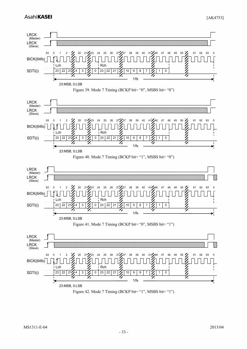
DSP Input Signals Setting The AK4753 has three input sources for DSP. The inputs of digital, analog and mix signals can be changed by SEL1-0 bits. In the initialization, the setting is SEL1-0 bits = “00” (Analog Input).
Digital-in
ADC
DSP Block
SW1
SEL1-0 bits
MIX
Figure 43. DSP Input source
SEL1 bit SEL0 bit DSP input source Note 0 0 Analog Default 0 1 Digital 1 0 MIX (Analog source)/2 + Digital source/2 1 1 N/A
Table 19. DSP Input Setting (N/A: Not Available) Bypass Mode The AK4753 has a BYPASS pin for the DSP bypass mode. When the BYPASS pin is “L”, the DSP blocks are enabled. When the BYPASS pin is “H”, the DSP blocks are disabled and the DATT outputs are skipped over the DSP blocks to the DAC.
BYPASS pin Mode H DSP Bypass Mode L Normal Operation
Table 20. Bypass Mode
DATT
DSP1 DAC1
DSP2 DAC2
BYPASS pin
“H”
“L”
“H”
“L”
“L”
“H”
“L”
“H”MIX
L+R 2
Figure 44. Bypass Mode
[AK4753]
MS1311-E-04 2013/04 - 35 -
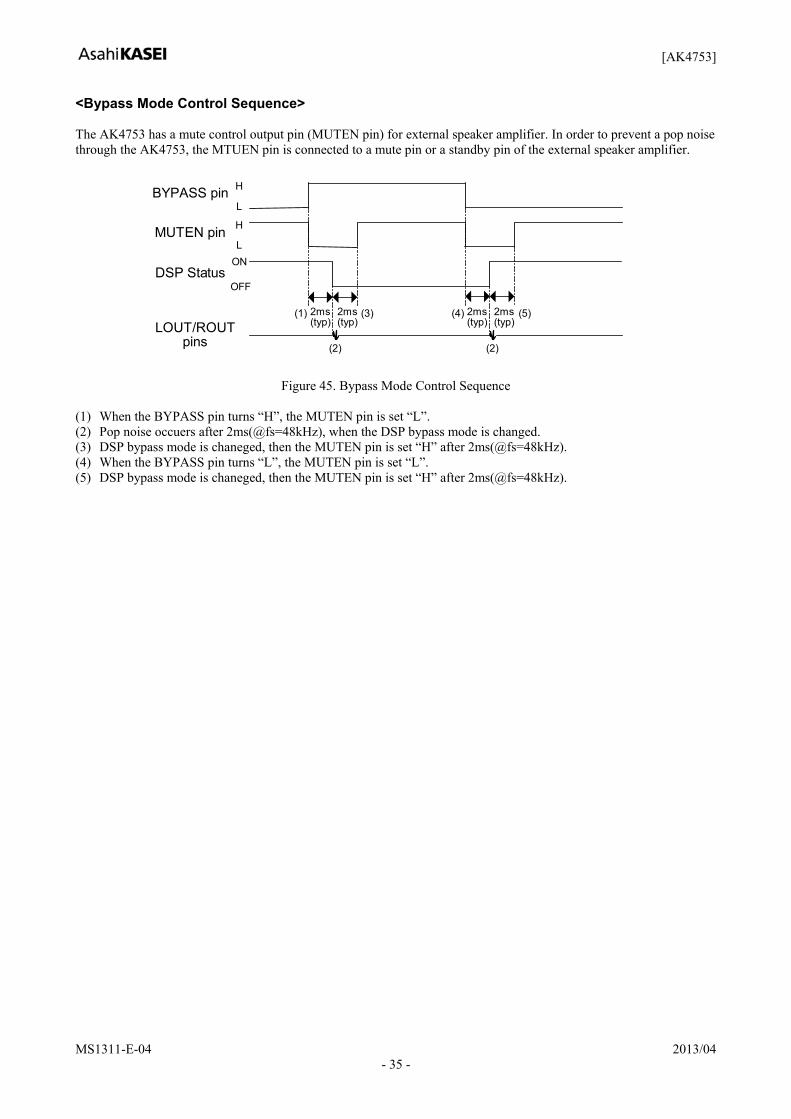
<Bypass Mode Control Sequence> The AK4753 has a mute control output pin (MUTEN pin) for external speaker amplifier. In order to prevent a pop noise through the AK4753, the MTUEN pin is connected to a mute pin or a standby pin of the external speaker amplifier.
BYPASS pin
MUTEN pin
DSP StatusON
OFF
H
L
H
L
LOUT/ROUTpins
(1)
(2)
(3) (4)
(2)
(5)2ms(typ)
2ms(typ)
2ms(typ)
2ms(typ)
Figure 45. Bypass Mode Control Sequence
(1) When the BYPASS pin turns “H”, the MUTEN pin is set “L”. (2) Pop noise occuers after 2ms(@fs=48kHz), when the DSP bypass mode is changed. (3) DSP bypass mode is chaneged, then the MUTEN pin is set “H” after 2ms(@fs=48kHz). (4) When the BYPASS pin turns “L”, the MUTEN pin is set “L”. (5) DSP bypass mode is chaneged, then the MUTEN pin is set “H” after 2ms(@fs=48kHz).
[AK4753]
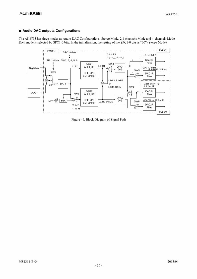
MS1311-E-04 2013/04 - 36 -
Audio DAC outputs Configurations The AK4753 has three modes as Audio DAC Configurations; Stereo Mode, 2.1-channels Mode and 4-channels Mode. Each mode is selected by SPC1-0 bits. In the initialization, the setting of the SPC1-0 bits is “00” (Stereo Mode).
Digital-in
ADC
DATT
DSP1 for L1, R1
HPF, LPF
EQ, Limiter
DAC1DIG
DSP2 for L2, R2
HPF, LPF
EQ, Limiter
DAC2DIG
L1, R1
SW1
SW2
1 0
SEL1-0 bits
SPC1-0 bits
SW3DAC1L
ANA
DAC2L ANA
DAC1R ANA
DAC2R ANA
SW40: R1 or R1+R2
−DAC2L or 2R2 or M
0: L1, R1 1: L1+L2, R1+R2
L1+M, R1+M
L1+L2, R1+R2
0: L, R
1: M, M
0
1
0
1
SW2, 3, 4, 5, 6
1: L2 or M
L2, R2 or M, M
or
L, R
L1 or L1+L2
−DAC1L or R1 SW5
0 1
SW6 0 −
1
or R1+R2 or R1+M
+
+
L+R2
PMDIG
PMLO2
PMLO1
MIX
−
M =
Figure 46. Block Diagram of Signal Path
[AK4753]
MS1311-E-04 2013/04 - 37 -
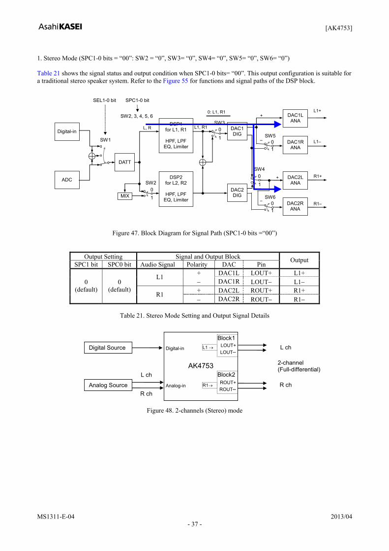
1. Stereo Mode (SPC1-0 bits = “00”: SW2 = “0”, SW3= “0”, SW4= “0”, SW5= “0”, SW6= “0”) Table 21 shows the signal status and output condition when SPC1-0 bits= “00”. This output configuration is suitable for a traditional stereo speaker system. Refer to the Figure 55 for functions and signal paths of the DSP block.
Digital-in
ADC
DATT
DSP1 for L1, R1
HPF, LPF
EQ, Limiter
DAC1DIG
DSP2 for L2, R2
HPF, LPF
EQ, Limiter
DAC2DIG
L1, R1
SW1
SW2
1 0
SEL1-0 bit SPC1-0 bit
SW3DAC1L
ANA
DAC2L ANA
DAC1R ANA
DAC2R ANA
SW4
0: L1, R1
0
1
0
1
SW2, 3, 4, 5, 6
L, R
L1+
SW5 0 −
1
SW6 0 −
1
+
+
L1−
R1+
R1−
MIX
Figure 47. Block Diagram for Signal Path (SPC1-0 bits =“00”)
Output Setting Signal and Output Block SPC1 bit SPC0 bit Audio Signal Polarity DAC Pin
Output
+ DAC1L LOUT+ L1+ L1 − DAC1R LOUT− L1− + DAC2L ROUT+ R1+
0 (default)
0 (default)
R1 − DAC2R ROUT− R1−
Table 21. Stereo Mode Setting and Output Signal Details
Block2
Block1
AK4753
LOUT+ L ch
R ch
LOUT−
ROUT+ROUT−
Analog Source
L ch
R ch Analog-in
Digital Source Digital-in L1 →
R1→
2-channel (Full-differential)
Figure 48. 2-channels (Stereo) mode
[AK4753]
MS1311-E-04 2013/04 - 38 -
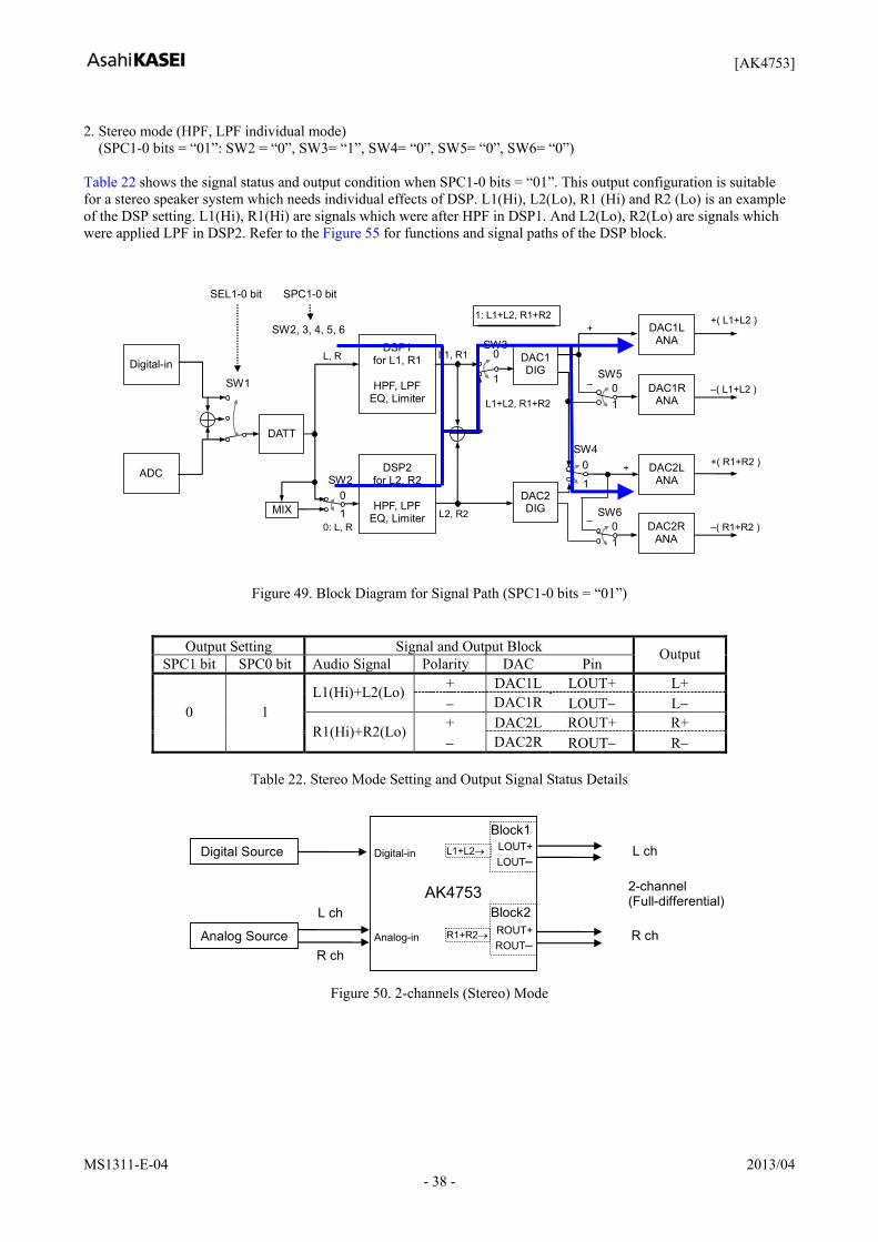
2. Stereo mode (HPF, LPF individual mode)
(SPC1-0 bits = “01”: SW2 = “0”, SW3= “1”, SW4= “0”, SW5= “0”, SW6= “0”) Table 22 shows the signal status and output condition when SPC1-0 bits = “01”. This output configuration is suitable for a stereo speaker system which needs individual effects of DSP. L1(Hi), L2(Lo), R1 (Hi) and R2 (Lo) is an example of the DSP setting. L1(Hi), R1(Hi) are signals which were after HPF in DSP1. And L2(Lo), R2(Lo) are signals which were applied LPF in DSP2. Refer to the Figure 55 for functions and signal paths of the DSP block.
Digital-in
ADC
DATT
DSP1 for L1, R1
HPF, LPF
EQ, Limiter
DAC1DIG
DSP2 for L2, R2
HPF, LPF
EQ, Limiter
DAC2DIG
L1, R1
SW1
SW2
1 0
SEL1-0 bit SPC1-0 bit
SW3DAC1L
ANA
DAC2L ANA
DAC1R ANA
DAC2R ANA
SW4
1: L1+L2, R1+R2
L1+L2, R1+R2
0: L, R
0
1
0
1
SW2, 3, 4, 5, 6
L2, R2
L, R
+( L1+L2 )
SW5 0 −
1
SW6 0 −
1
+
+
−( L1+L2 )
+( R1+R2 )
−( R1+R2 )
MIX
Figure 49. Block Diagram for Signal Path (SPC1-0 bits = “01”)
Output Setting Signal and Output Block SPC1 bit SPC0 bit Audio Signal Polarity DAC Pin
Output
+ DAC1L LOUT+ L+ L1(Hi)+L2(Lo)− DAC1R LOUT− L− + DAC2L ROUT+ R+
0 1 R1(Hi)+R2(Lo)
− DAC2R ROUT− R−
Table 22. Stereo Mode Setting and Output Signal Status Details
Block2
Block1
AK4753
LOUT+ L ch
R ch
LOUT−
ROUT+ROUT−
Analog Source
L ch
R ch Analog-in
Digital Source Digital-in L1+L2→
R1+R2→
2-channel (Full-differential)
Figure 50. 2-channels (Stereo) Mode
[AK4753]
MS1311-E-04 2013/04 - 39 -
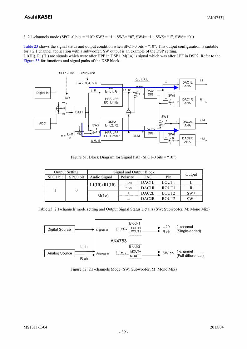
3. 2.1-channels mode (SPC1-0 bits = “10”: SW2 = “1”, SW3= “0”, SW4= “1”, SW5= “1”, SW6= “0”) Table 23 shows the signal status and output condition when SPC1-0 bits = “10”. This output configuration is suitable for a 2.1 channel application with a subwoofer. SW output is an example of the DSP setting. L1(Hi), R1(Hi) are signals which were after HPF in DSP1. M(Lo) is signal which was after LPF in DSP2. Refer to the Figure 55 for functions and signal paths of the DSP block.
Digital-in
ADC
DATT
DSP1 for L1, R1
HPF, LPF
EQ, Limiter
DAC1DIG
DSP2 for L2, R2
HPF, LPF
EQ, Limiter
DAC2DIG
L1, R1
SW1
SW2
1
SEL1-0 bit SPC1-0 bit
SW3DAC1L
ANA
DAC2L ANA
DAC1R ANA
DAC2R ANA
SW4
0: L1, R1,
1: M, M
0
1
SW2, 3, 4, 5, 6
M, M
L, R
L1
SW5 −
1
SW6 0 −
+
+
R1
+ M
− M L+R
2 MIX
M =
Figure 51. Block Diagram for Signal Path (SPC1-0 bits = “10”)
Output Setting Signal and Output Block SPC1 bit SPC0 bit Audio Signal Polarity DAC Pin
Output
non DAC1L LOUT1 L L1(Hi)+R1(Hi)non DAC1R ROUT1 R + DAC2L LOUT2 SW+
1 0 M(Lo)
− DAC2R ROUT2 SW−
Table 23. 2.1-channels mode setting and Output Signal Status Details (SW: Subwoofer, M: Mono Mix)
Block2
Block1
AK4753
LOUT1 L ch
SW ch
ROUT1
MOUT+MOUT−
Analog Source
L ch
R ch Analog-in
Digital Source Digital-in L1,R1→
M→
R ch
1-channel (Full-differential)
2-channel (Single-ended)
Figure 52. 2.1-channels Mode (SW: Subwoofer, M: Mono Mix)
[AK4753]
MS1311-E-04 2013/04 - 40 -
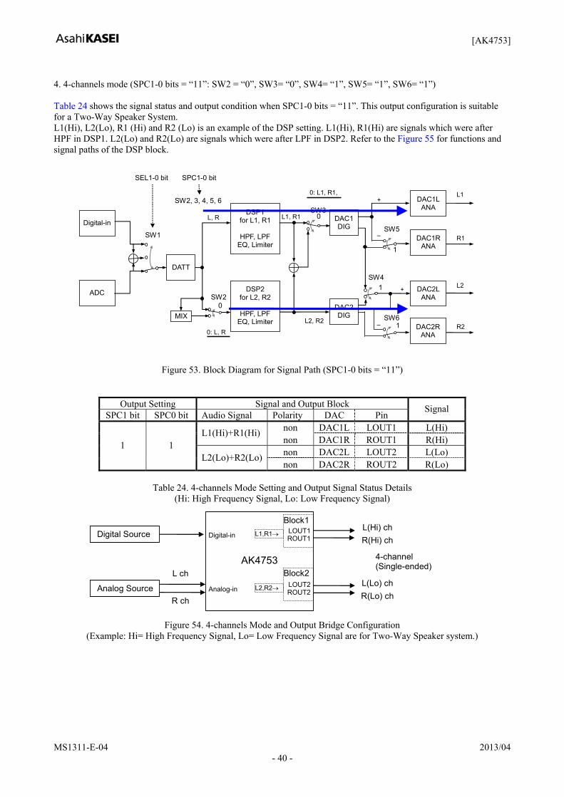
4. 4-channels mode (SPC1-0 bits = “11”: SW2 = “0”, SW3= “0”, SW4= “1”, SW5= “1”, SW6= “1”) Table 24 shows the signal status and output condition when SPC1-0 bits = “11”. This output configuration is suitable for a Two-Way Speaker System. L1(Hi), L2(Lo), R1 (Hi) and R2 (Lo) is an example of the DSP setting. L1(Hi), R1(Hi) are signals which were after HPF in DSP1. L2(Lo) and R2(Lo) are signals which were after LPF in DSP2. Refer to the Figure 55 for functions and signal paths of the DSP block.
Digital-in
ADC
DATT
DSP1 for L1, R1
HPF, LPF
EQ, Limiter
DAC1DIG
DSP2 for L2, R2
HPF, LPF
EQ, Limiter
DAC2DIG
L1, R1
SW1
SW2
0
SEL1-0 bit SPC1-0 bit
SW3DAC1L
ANA
DAC2L ANA
DAC1R ANA
DAC2R ANA
SW4
0: L1, R1,
0: L, R
0
1
SW2, 3, 4, 5, 6
L2, R2
L, R
L1
SW5 −
1
SW6 − 1
+
+
R1
L2
R2 MIX
Figure 53. Block Diagram for Signal Path (SPC1-0 bits = “11”)
Output Setting Signal and Output Block SPC1 bit SPC0 bit Audio Signal Polarity DAC Pin
Signal
non DAC1L LOUT1 L(Hi) L1(Hi)+R1(Hi)non DAC1R ROUT1 R(Hi) non DAC2L LOUT2 L(Lo)
1 1 L2(Lo)+R2(Lo)
non DAC2R ROUT2 R(Lo)
Table 24. 4-channels Mode Setting and Output Signal Status Details (Hi: High Frequency Signal, Lo: Low Frequency Signal)
Block2
Block1
AK4753
LOUT1 L(Hi) chROUT1
LOUT2ROUT2Analog Source
L ch
R ch Analog-in
Digital Source Digital-in L1,R1→R(Hi) ch
L2,R2→L(Lo) chR(Lo) ch
4-channel (Single-ended)
Figure 54. 4-channels Mode and Output Bridge Configuration
(Example: Hi= High Frequency Signal, Lo= Low Frequency Signal are for Two-Way Speaker system.)
[AK4753]
MS1311-E-04 2013/04 - 41 -
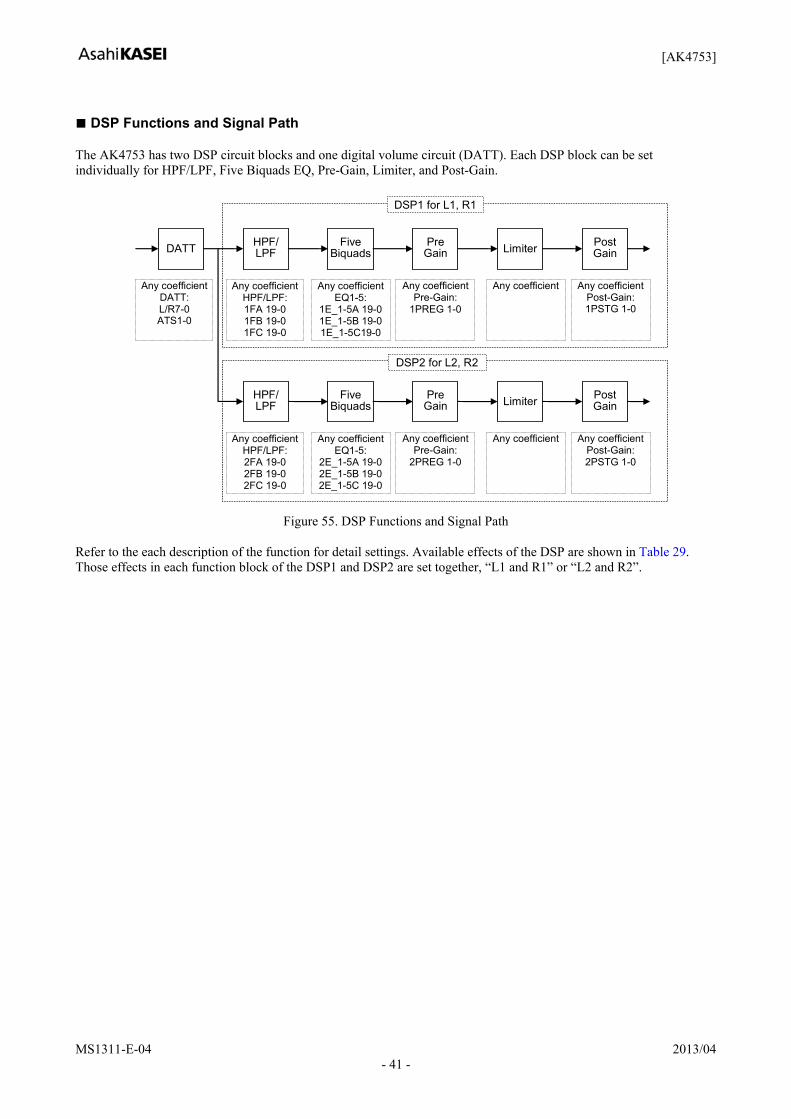
DSP Functions and Signal Path The AK4753 has two DSP circuit blocks and one digital volume circuit (DATT). Each DSP block can be set individually for HPF/LPF, Five Biquads EQ, Pre-Gain, Limiter, and Post-Gain.
HPF/ LPF
Pre Gain
Any coefficient HPF/LPF: 1FA 19-0 1FB 19-0 1FC 19-0
Any coefficientEQ1-5:
1E_1-5A 19-01E_1-5B 19-01E_1-5C19-0
LimiterFive BiquadsDATT
Any coefficient DATT: L/R7-0 ATS1-0
Any coefficientPre-Gain:
1PREG 1-0
Any coefficient
HPF/ LPF
Pre Gain
Any coefficient HPF/LPF: 2FA 19-0 2FB 19-0 2FC 19-0
Any coefficientEQ1-5:
2E_1-5A 19-02E_1-5B 19-02E_1-5C 19-0
LimiterFive Biquads
Any coefficientPre-Gain:
2PREG 1-0
Any coefficient
DSP1 for L1, R1
DSP2 for L2, R2
Post Gain
Any coefficient Post-Gain: 1PSTG 1-0
Post Gain
Any coefficient Post-Gain: 2PSTG 1-0
Figure 55. DSP Functions and Signal Path
Refer to the each description of the function for detail settings. Available effects of the DSP are shown in Table 29. Those effects in each function block of the DSP1 and DSP2 are set together, “L1 and R1” or “L2 and R2”.
[AK4753]
MS1311-E-04 2013/04 - 42 -
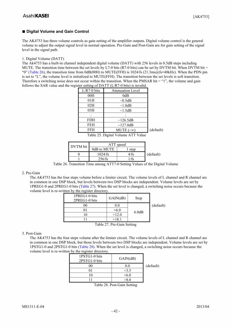
Digital Volume and Gain Control The AK4753 has three volume controls as gain setting of the amplifier outputs. Digital volume control is the general volume to adjust the output signal level in normal operation. Pre-Gain and Post-Gain are for gain setting of the signal level in the signal path. 1. Digital Volume (DATT) The Ak4753 has a built-in channel independent digital volume (DATT) with 256 levels in 0.5dB steps including MUTE. The transition time between the set levels by L7-0 bits (R7-0 bits) can be set by DVTM bit. When DVTM bit = “0” (Table 26), the transition time from 0dB(00H) to MUTE(FFH) is 1024/fs (21.3ms@fs=48kHz). When the PDN pin is set to “L”, the volume level is initialized to MUTE(FFH). The transition between the set levels is soft transition. Therefore a switching noise does not occur within the transition. When the PMSAR bit = “1”, the volume and gain follows the SAR value and the register setting of DATT (L/R7-0 bits) is invalid.
L/R7-0 bits Attenuation Level 00H 0dB 01H −0.5dB 02H −1.0dB 03H −1.5dB
: : FDH −126.5dB FEH −127.0dB FFH MUTE (−∞) (default)
Table 25. Digital Volume ATT Value
ATT speed DVTM bit 0dB to MUTE 1 step
0 1024/fs 4/fs (default)1 256/fs 1/fs
Table 26. Transition Time among ATT7-0 Setting Values of the Digital Volume
2. Pre-Gain The AK4753 has the four steps volume before a limiter circuit. The volume levels of L channel and R channel are in common in one DSP block, but levels between two DSP blocks are independent. Volume levels are set by 1PREG1-0 and 2PREG1-0 bits (Table 27). When the set level is changed, a switching noise occurs because the volume level is re-written by the register directory.
1PREG1-0 bits 2PREG1-0 bits GAIN(dB) Step
00 0.0 (default) 01 +6.0 10 +12.0 11 +18.1
6.0dB
Table 27. Pre-Gain Setting
3. Post-Gain
The AK4753 has the four steps volume after the limiter circuit. The volume levels of L channel and R channel are in common in one DSP block, but those levels between two DSP blocks are independent. Volume levels are set by 1PSTG1-0 and 2PSTG1-0 bits (Table 28). When the set level is changed, a switching noise occurs because the volume level is re-written by the register directory.
1PSTG1-0 bits 2PSTG1-0 bits GAIN(dB)
00 0.0 (default)01 +3.5 10 +6.0 11 +8.0
Table 28. Post-Gain Setting
[AK4753]
MS1311-E-04 2013/04 - 43 -
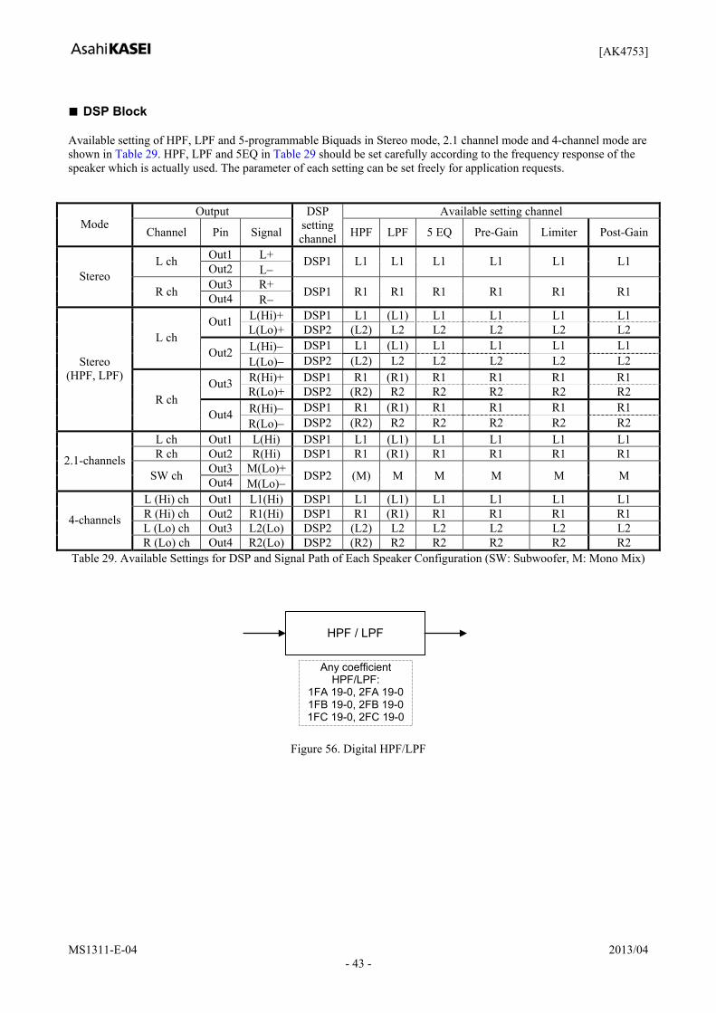
DSP Block Available setting of HPF, LPF and 5-programmable Biquads in Stereo mode, 2.1 channel mode and 4-channel mode are shown in Table 29. HPF, LPF and 5EQ in Table 29 should be set carefully according to the frequency response of the speaker which is actually used. The parameter of each setting can be set freely for application requests.
Output Available setting channel Mode
Channel Pin Signal
DSP setting channel HPF LPF 5 EQ Pre-Gain Limiter Post-Gain
Out1 L+ L ch Out2 L− DSP1 L1 L1 L1 L1 L1 L1
Out3 R+ Stereo
R ch Out4 R− DSP1 R1 R1 R1 R1 R1 R1
L(Hi)+ DSP1 L1 (L1) L1 L1 L1 L1 Out1 L(Lo)+ DSP2 (L2) L2 L2 L2 L2 L2 L(Hi)− DSP1 L1 (L1) L1 L1 L1 L1 L ch
Out2 L(Lo)− DSP2 (L2) L2 L2 L2 L2 L2 R(Hi)+ DSP1 R1 (R1) R1 R1 R1 R1 Out3 R(Lo)+ DSP2 (R2) R2 R2 R2 R2 R2 R(Hi)− DSP1 R1 (R1) R1 R1 R1 R1
Stereo (HPF, LPF)
R ch Out4
R(Lo)− DSP2 (R2) R2 R2 R2 R2 R2 L ch Out1 L(Hi) DSP1 L1 (L1) L1 L1 L1 L1 R ch Out2 R(Hi) DSP1 R1 (R1) R1 R1 R1 R1
Out3 M(Lo)+ 2.1-channels SW ch Out4 M(Lo)−
DSP2 (M) M M M M M
L (Hi) ch Out1 L1(Hi) DSP1 L1 (L1) L1 L1 L1 L1 R (Hi) ch Out2 R1(Hi) DSP1 R1 (R1) R1 R1 R1 R1 L (Lo) ch Out3 L2(Lo) DSP2 (L2) L2 L2 L2 L2 L2
4-channels
R (Lo) ch Out4 R2(Lo) DSP2 (R2) R2 R2 R2 R2 R2 Table 29. Available Settings for DSP and Signal Path of Each Speaker Configuration (SW: Subwoofer, M: Mono Mix)
HPF / LPF
Any coefficient HPF/LPF:
1FA 19-0, 2FA 19-01FB 19-0, 2FB 19-01FC 19-0, 2FC 19-0
Figure 56. Digital HPF/LPF
[AK4753]
MS1311-E-04 2013/04 - 44 -
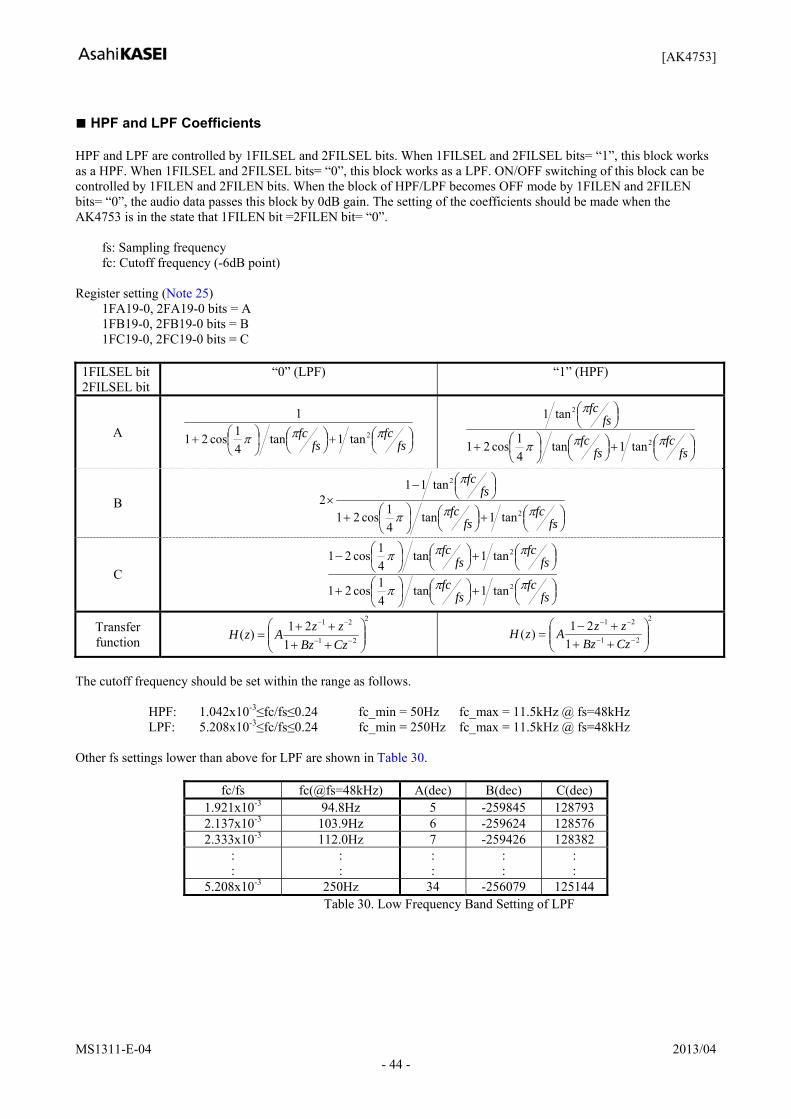
HPF and LPF Coefficients HPF and LPF are controlled by 1FILSEL and 2FILSEL bits. When 1FILSEL and 2FILSEL bits= “1”, this block works as a HPF. When 1FILSEL and 2FILSEL bits= “0”, this block works as a LPF. ON/OFF switching of this block can be controlled by 1FILEN and 2FILEN bits. When the block of HPF/LPF becomes OFF mode by 1FILEN and 2FILEN bits= “0”, the audio data passes this block by 0dB gain. The setting of the coefficients should be made when the AK4753 is in the state that 1FILEN bit =2FILEN bit= “0”.
fs: Sampling frequency fc: Cutoff frequency (-6dB point)
Register setting (Note 25)
1FA19-0, 2FA19-0 bits = A 1FB19-0, 2FB19-0 bits = B 1FC19-0, 2FC19-0 bits = C
1FILSEL bit 2FILSEL bit
“0” (LPF) “1” (HPF)
A ⎟⎠⎞⎜
⎝⎛+⎟
⎠⎞⎜
⎝⎛⎟
⎠⎞
⎜⎝⎛+ fs
fcfs
fc πππ 2tan1tan41cos21
1
⎟⎠⎞⎜
⎝⎛+⎟
⎠⎞⎜
⎝⎛⎟
⎠⎞
⎜⎝⎛+
⎟⎠⎞⎜
⎝⎛
fsfc
fsfc
fsfc
πππ
π
2
2
tan1tan41cos21
tan1
B ⎟⎠⎞⎜
⎝⎛+⎟
⎠⎞⎜
⎝⎛⎟
⎠⎞
⎜⎝⎛+
⎟⎠⎞⎜
⎝⎛−
×
fsfc
fsfc
fsfc
πππ
π
2
2
tan1tan41cos21
tan112
C ⎟⎠⎞⎜
⎝⎛+⎟
⎠⎞⎜
⎝⎛⎟
⎠⎞
⎜⎝⎛+
⎟⎠⎞⎜
⎝⎛+⎟
⎠⎞⎜
⎝⎛⎟
⎠⎞
⎜⎝⎛−
fsfc
fsfc
fsfc
fsfc
πππ
πππ
2
2
tan1tan41cos21
tan1tan41cos21
Transfer function
2
21
21
121)( ⎟⎟
⎠
⎞⎜⎜⎝
⎛++++
= −−
−−
CzBzzzAzH
2
21
21
121)( ⎟⎟
⎠
⎞⎜⎜⎝
⎛+++−
= −−
−−
CzBzzzAzH
The cutoff frequency should be set within the range as follows.
HPF: 1.042x10⁻³≤fc/fs≤0.24 fc_min = 50Hz fc_max = 11.5kHz @ fs=48kHz LPF: 5.208x10⁻³≤fc/fs≤0.24 fc_min = 250Hz fc_max = 11.5kHz @ fs=48kHz
Other fs settings lower than above for LPF are shown in Table 30.
fc/fs fc(@fs=48kHz) A(dec) B(dec) C(dec) 1.921x10⁻³ 94.8Hz 5 -259845 128793 2.137x10⁻³ 103.9Hz 6 -259624 128576 2.333x10⁻³ 112.0Hz 7 -259426 128382
: :
: :
: :
: :
: :
5.208x10⁻³ 250Hz 34 -256079 125144 Table 30. Low Frequency Band Setting of LPF

[AK4753]
MS1311-E-04 2013/04 - 45 -
Five Programmable Biquads This block can be used as an equalizer or notch filter. 5-band equalizer (EQ1, EQ2, EQ3, EQ4 and EQ5) is ON/OFF independently by EQ1, EQ2, EQ3, EQ4 and EQ5 bits. When the equalizer is OFF, the audio data passes this block by 0dB gain. E1A19-0, E1B19-0 and E1C19-0 bits set the coefficient of EQ1. E2A19-0, E2B19-0 and E2C19-0 bits set the coefficient of EQ2. E3A19-0, E3B19-0 and E3C19-0 bits set the coefficient of EQ3. E4A19-0, E4B19-0 and E4C19-0 bits set the coefficient of EQ4. E5A19-0, E5B19-0 and E5C19-0 bits set the coefficient of EQ5. EQx (x=1~5) coefficient should be set when EQx bit = “0” or PMDAC bit = “0”. When the SA2 bit = “1”, K1 gain must be set to “1” for the DSP channel selected by the SA2SEL bit.
fs: Sampling frequency fo1 ~ fo5: Center frequency fb1 ~ fb5: Band width where the gain is 3dB different from center frequency K1 ~ K5 : Gain ( -1 ≤ Kn < 3 )
Register setting (Note 25) EQ1: E1A19-0 bits =A1, E1B19-0 bits =B1, E1C19-0 bits =C1 EQ2: E2A19-0 bits =A2, E2B19-0 bits =B2, E2C19-0 bits =C2 EQ3: E3A19-0 bits =A3, E3B19-0 bits =B3, E3C19-0 bits =C3 EQ4: E4A19-0 bits =A4, E4B19-0 bits =B4, E4C19-0 bits =C4 EQ5: E5A19-0 bits =A5, E5B19-0 bits =B5, E5C19-0 bits =C5 (MSB=E1A19, E1B19, E1C19, E2A19, E2B19, E2C19, E3A19, E3B19, E3C19, E4A19, E4B19, E4C19, E5A19, E5B19, E5C19; LSB= E1A0, E1B0, E1C0, E2A0, E2B0, E2C0, E3A0, E3B0, E3C0, E4A0, E4B0, E4C0, E5A0, E5B0, E5C0)
An = Kn x
tan (πfbn/fs)
1 + tan (πfbn/fs) Bn = cos(2π fon/fs) x
2
1 + tan (πfbn/fs), Cn =
1 − tan (πfbn/fs)
1 + tan (πfbn/fs),
(n = 1, 2, 3, 4, 5)
Transfer function
hn (z) = An
1 − z −2
1− Bnz −1− Cnz −2
H(z) = 1 + h1(z) + h2(z) + h3(z) + h4(z) + h5(z)
(n = 1, 2, 3, 4, 5)
The fbn should be set within the range as follows.
fbn/fs ≤ 0.25 The f0n (center frequency) should be set within the range as follows.
3.125x10⁻³ ≤ f0n/fs < 0.4969 When the f0n/fs is less than 3.125x10⁻³, the step width of the f0n which can be set up becomes the biggest in the case of fbn/fs=0.25. (Table 31)
f0n/fs f0n(@fs=48kHz) An (dec) (Kn=-1) Bn (dec) Cn (dec) 8.542x10 -4 41Hz -65536 131070 0 1.083x10 -3 52Hz -65536 131069 0 1.229x10 -3 59Hz -65536 131068 0
: : : : : 3.125x10 -3 150Hz -65536 131047 0
Table 31. The Center Frequency in the low frequency band (when the coefficients of An, Bn and Cn is fbn/fs=0.25)
Note 25. Translation the filter coefficient calculated by the equations above from real number to binary code (2’s
complement) X = (Real number of filter coefficient calculated by the equations above) x 217 X should be rounded to integer, and then should be translated to binary code (2’s complement). MSB of each filter coefficient setting register is sign bit.
[AK4753]
MS1311-E-04 2013/04 - 46 -
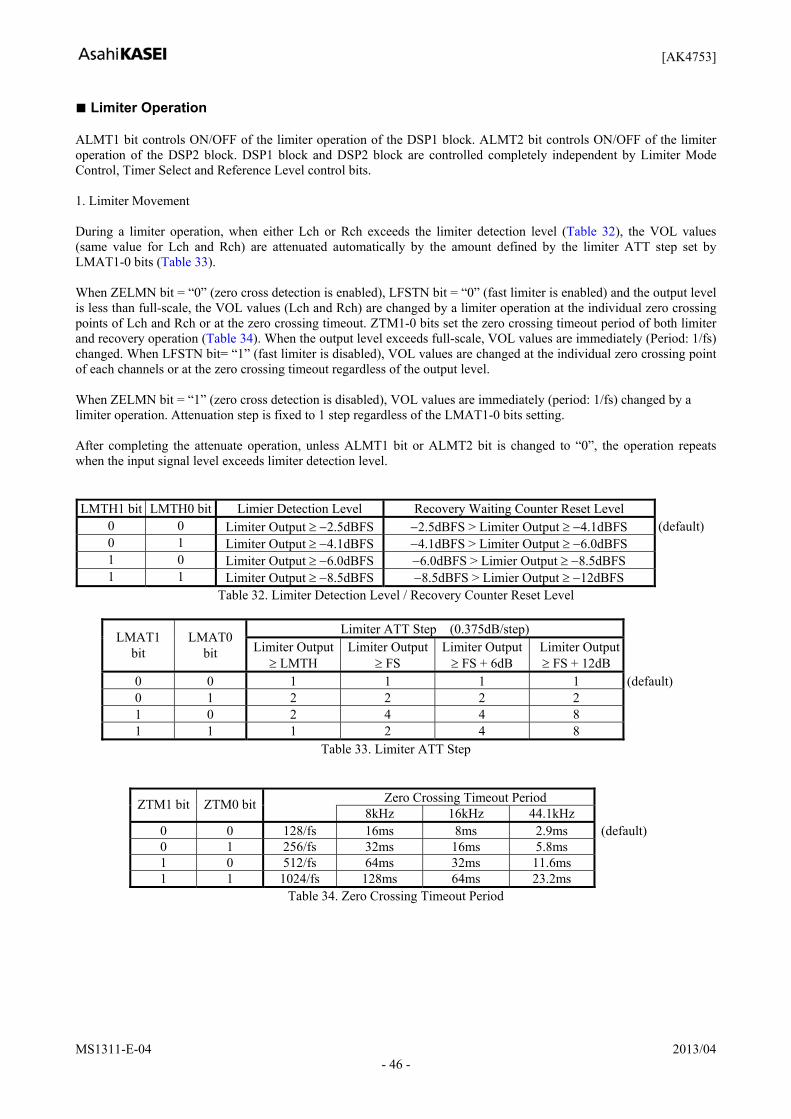
Limiter Operation ALMT1 bit controls ON/OFF of the limiter operation of the DSP1 block. ALMT2 bit controls ON/OFF of the limiter operation of the DSP2 block. DSP1 block and DSP2 block are controlled completely independent by Limiter Mode Control, Timer Select and Reference Level control bits. 1. Limiter Movement During a limiter operation, when either Lch or Rch exceeds the limiter detection level (Table 32), the VOL values (same value for Lch and Rch) are attenuated automatically by the amount defined by the limiter ATT step set by LMAT1-0 bits (Table 33). When ZELMN bit = “0” (zero cross detection is enabled), LFSTN bit = “0” (fast limiter is enabled) and the output level is less than full-scale, the VOL values (Lch and Rch) are changed by a limiter operation at the individual zero crossing points of Lch and Rch or at the zero crossing timeout. ZTM1-0 bits set the zero crossing timeout period of both limiter and recovery operation (Table 34). When the output level exceeds full-scale, VOL values are immediately (Period: 1/fs) changed. When LFSTN bit= “1” (fast limiter is disabled), VOL values are changed at the individual zero crossing point of each channels or at the zero crossing timeout regardless of the output level. When ZELMN bit = “1” (zero cross detection is disabled), VOL values are immediately (period: 1/fs) changed by a limiter operation. Attenuation step is fixed to 1 step regardless of the LMAT1-0 bits setting. After completing the attenuate operation, unless ALMT1 bit or ALMT2 bit is changed to “0”, the operation repeats when the input signal level exceeds limiter detection level. LMTH1 bit LMTH0 bit Limier Detection Level Recovery Waiting Counter Reset Level
0 0 Limiter Output ≥ −2.5dBFS −2.5dBFS > Limiter Output ≥ −4.1dBFS (default)0 1 Limiter Output ≥ −4.1dBFS −4.1dBFS > Limiter Output ≥ −6.0dBFS 1 0 Limiter Output ≥ −6.0dBFS −6.0dBFS > Limier Output ≥ −8.5dBFS 1 1 Limiter Output ≥ −8.5dBFS −8.5dBFS > Limier Output ≥ −12dBFS
Table 32. Limiter Detection Level / Recovery Counter Reset Level
Limiter ATT Step (0.375dB/step) LMAT1 bit
LMAT0 bit Limiter Output
≥ LMTH Limiter Output
≥ FS Limiter Output
≥ FS + 6dB Limiter Output ≥ FS + 12dB
0 0 1 1 1 1 (default) 0 1 2 2 2 2 1 0 2 4 4 8 1 1 1 2 4 8
Table 33. Limiter ATT Step
Zero Crossing Timeout Period ZTM1 bit ZTM0 bit 8kHz 16kHz 44.1kHz
0 0 128/fs 16ms 8ms 2.9ms (default) 0 1 256/fs 32ms 16ms 5.8ms 1 0 512/fs 64ms 32ms 11.6ms 1 1 1024/fs 128ms 64ms 23.2ms
Table 34. Zero Crossing Timeout Period
[AK4753]
MS1311-E-04 2013/04 - 47 -
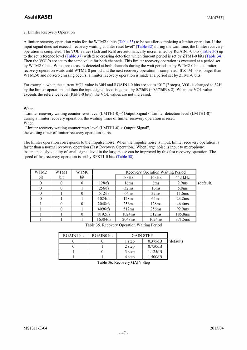
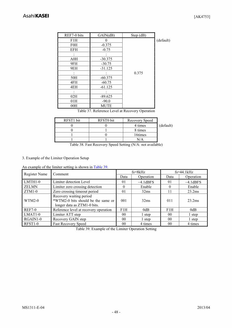
2. Limiter Recovery Operation A limiter recovery operation waits for the WTM2-0 bits (Table 35) to be set after completing a limiter operation. If the input signal does not exceed “recovery waiting counter reset level” (Table 32) during the wait time, the limiter recovery operation is completed. The VOL values (Lch and Rch) are automatically incremented by RGAIN1-0 bits (Table 36) up to the set reference level (Table 37) with zero crossing detection which timeout period is set by ZTM1-0 bits (Table 34). Then the VOL’s are set to the same value for both channels. This limiter recovery operation is executed at a period set by WTM2-0 bits. When zero cross is detected at both channels during the wait period set by WTM2-0 bits, a limiter recovery operation waits until WTM2-0 period and the next recovery operation is completed. If ZTM1-0 is longer than WTM2-0 and no zero crossing occurs, a limiter recovery operation is made at a period set by ZTM1-0 bits. For example, when the current VOL value is 30H and RGAIN1-0 bits are set to “01” (2 steps), VOL is changed to 32H by the limiter operation and then the input signal level is gained by 0.75dB (=0.375dB x 2). When the VOL value exceeds the reference level (REF7-0 bits), the VOL values are not increased. When “Limiter recovery waiting counter reset level (LMTH1-0) ≤ Output Signal < Limiter detection level (LMTH1-0)” during a limiter recovery operation, the waiting timer of limiter recovery operation is reset. When “Limiter recovery waiting counter reset level (LMTH1-0) > Output Signal”, the waiting timer of limiter recovery operation starts. The limiter operation corresponds to the impulse noise. When the impulse noise is input, limiter recovery operation is faster than a normal recovery operation (Fast Recovery Operation). When large noise is input to microphone instantaneously, quality of small signal level in the large noise can be improved by this fast recovery operation. The speed of fast recovery operation is set by RFST1-0 bits (Table 38).
Recovery Operation Waiting Period WTM2 bit
WTM1 bit
WTM0 bit 8kHz 16kHz 44.1kHz
0 0 0 128/fs 16ms 8ms 2.9ms (default) 0 0 1 256/fs 32ms 16ms 5.8ms 0 1 0 512/fs 64ms 32ms 11.6ms 0 1 1 1024/fs 128ms 64ms 23.2ms 1 0 0 2048/fs 256ms 128ms 46.4ms 1 0 1 4096/fs 512ms 256ms 92.9ms 1 1 0 8192/fs 1024ms 512ms 185.8ms 1 1 1 16384/fs 2048ms 1024ms 371.5ms
Table 35. Recovery Operation Waiting Period
RGAIN1 bit RGAIN0 bit GAIN STEP 0 0 1 step 0.375dB (default) 0 1 2 step 0.750dB 1 0 3 step 1.125dB 1 1 4 step 1.500dB
Table 36. Recovery GAIN Step
[AK4753]
MS1311-E-04 2013/04 - 48 -
REF7-0 bits GAIN(dB) Step (dB)
F1H 0 (default) F0H -0.375 EFH -0.75
: : A0H -30.375 9FH -30.75 9EH -31.125
: : 0.375 50H -60.375 4FH -60.75 4EH -61.125
: : 02H -89.625 01H -90.0 00H MUTE
Table 37. Reference Level at Recovery Operation
RFST1 bit RFST0 bit Recovery Speed 0 0 4 times (default) 0 1 8 times 1 0 16times 1 1 N/A
Table 38. Fast Recovery Speed Setting (N/A: not available) 3. Example of the Limiter Operation Setup An example of the limiter setting is shown in Table 39.
fs=8kHz fs=44.1kHz Register Name Comment Data Operation Data Operation
LMTH1-0 Limiter detection Level 01 −4.1dBFS 01 −4.1dBFS ZELMN Limiter zero crossing detection 0 Enable 0 Enable ZTM1-0 Zero crossing timeout period 01 32ms 11 23.2ms
WTM2-0 Recovery waiting period *WTM2-0 bits should be the same or
longer data as ZTM1-0 bits. 001 32ms 011 23.2ms
REF7-0 Reference level at recovery operation F1H 0dB F1H 0dB LMAT1-0 Limiter ATT step 00 1 step 00 1 step RGAIN1-0 Recovery GAIN step 00 1 step 00 1 step RFST1-0 Fast Recovery Speed 00 4 times 00 4 times
Table 39. Example of the Limiter Operation Setting

[AK4753]
MS1311-E-04 2013/04 - 49 -
Line Outputs Line outputs of the AK4753 have internal resisters in series. The resister value is 200Ω (typ). By just connecting small capacitors between VSS1 and each the LOUT1/2 or ROUT1/2 pin, high frequency noise will be significantly reduced.
LOUT1/2ROUT1/2
C 150pF(max)
200Ω (typ) 1μF
AK4753
Figure 57. External Circuit for Stereo Line Outputs (In case of using high frequency noise reduction circuit.) <Line Outputs Control Sequence> The AK4753 has a mute control output pin (MUTEN pin) for external speaker amplifier. In order to prevent a pop noise through the AK4753, the MTUEN pin is connected to a mute pin or a standby pin of the external speaker amplifier. In the PLL mode, when the PLL is unlocked or the line outputs are disabled, the MUTEN outputs “L”. When the PLL is locked and the line outputs are enabled, the MUTEN outputs “H”.
PMLO1/2 bit
MUTEN pin
LOUT1/2, ROUT1/2 pins Normal Output
4ms (typ)
MUTE OffMUTE On MUTE On
Figure 58. Line Outputs Control Sequence

[AK4753]
MS1311-E-04 2013/04 - 50 -
SAR 8-bit ADC The AK4753 incorporates a 8-bit successive approximation resistor A/D converter for DC measurement. By connecting potentiometers, the gain of DATT can be controlled by SAIN1and the gain of EQ1 can be controlled by SAIN2. The A/D converter output for the SAIN1 pin is a straight binary format as shown in Table 40.
Input Voltage Output Code Attenuation Level (AVDD−1.0LSB) ~ AVDD 00H 0dB (AVDD−2.0LSB) ~ (AVDD−1.0LSB) 01H -0.5dB
: : : 1.0LSB ~ 2.0LSB FEH -127dB
0 ~ 1.0LSB FFH MUTE (−∞) Table 40. Output Code for the SAIN1 Pin
The A/D converter output for the SAIN2 pin is a straight binary format as shown in Table 41.
Input Voltage Output Code (AVDD−1.0LSB) ~ AVDD 00H (AVDD-2.0LSB) ~ (AVDD−1.0LSB) 01H
: : 1.0LSB ~ 2.0LSB FEH
0 ~ 1.0LSB FFH Table 41. Output Code for the SAIN2 pin
Output Code Gain@EQ1 K1@EQ1 00H ~ 04H 05H ~ 09H
+12.0dB 2.981
0AH ~ 0EH +11.5dB 2.758 0FH ~ 13H +11.0dB 2.548 14H ~ 18H +10.5dB 2.350
: : : 7DH ~ 81H 0dB 0
: : : E6H ~ EAH -10.5dB -0.701 EBH ~ EFH -11.0dB -0.718 F0H ~ F4H -11.5dB -0.734 F5H ~ F9H FAH ~ FFH -12.0dB -0.749
Table 42. Gain Setting of EQ1
SA2SEL bit K1 0 DSP1 (default) 1 DSP2
Table 43. Source for the SAIN2 pin
SA2 bit SAIN2 pin 0 Disable (default) 1 Enable
Table 44. Configuration for the SAIN2 pin
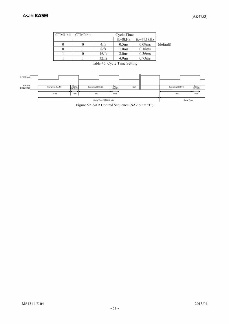
[AK4753]
MS1311-E-04 2013/04 - 51 -
Cycle Time CTM1 bit CTM0 bit
fs=8kHz fs=44.1kHz
0 0 4/fs 0.5ms 0.09ms (default) 0 1 8/fs 1.0ms 0.18ms 1 0 16/fs 2.0ms 0.36ms 1 1 32/fs 4.0ms 0.73ms
Table 45. Cycle Time Setting
LRCK pin
1/8fs
Conv (SAIN1) Sampling (SAIN1) Idol
Cycle Time (CTM1-0 bits) Cycle Time
Internal Sequence
7/8fs 1/8fs
Conv (SAIN2) Sampling (SAIN2)
7/8fs
Sampling (SAIN1)
7/8fs
Conv (SAIN1)
1/8fs
Figure 59. SAR Control Sequence (SA2 bit = “1”)
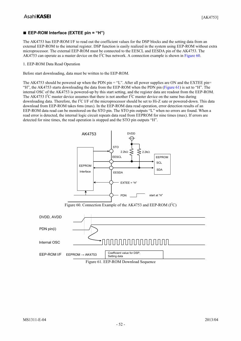
[AK4753]
MS1311-E-04 2013/04 - 52 -
EEP-ROM Interface (EXTEE pin = “H”) The AK4753 has EEP-ROM I/F to read out the coefficient values for the DSP blocks and the setting data from an external EEP-ROM to the internal register. DSP function is easily realized in the system using EEP-ROM without extra microprocessor. The external EEP-ROM must be connected to the EESCL and EESDA pin of the AK4753. The AK4753 can operate as a master device on the I2C bus network. A connection example is shown in Figure 60. 1. EEP-ROM Data Read Operation Before start downloading, data must be written to the EEP-ROM. The AK4753 should be powered up when the PDN pin = “L”. After all power supplies are ON and the EXTEE pin= “H”, the AK4753 starts downloading the data from the EEP-ROM when the PDN pin (Figure 61) is set to “H”. The internal OSC of the AK4753 is powered-up by this start setting, and the register data are readout from the EEP-ROM. The AK4753 I2C master device assumes that there is not another I2C master device on the same bus during downloading data. Therefore, the I2C I/F of the microprocessor should be set to Hi-Z sate or powered-down. This data download from EEP-ROM takes 6ms (max). In the EEP-ROM data read operation, error detection results of an EEP-ROM data read can be monitored on the STO pin. The STO pin outputs “L” when no errors are found. When a read error is detected, the internal logic circuit repeats data read from EEPROM for nine times (max). If errors are detected for nine times, the read operation is stopped and the STO pin outputs “H”.
EEPROM
SCL
SDAEEPROM
Interface EESDA
EESCL
EXTEE = “H”
AK4753
2.2kΩ
DVDD
PDN
2.2kΩ
start at “H”
STO
Figure 60. Connection Example of the AK4753 and EEP-ROM (I2C)
PDN pin(i)
DVDD, AVDD
Coefficient value for DSP, Setting data EEP-ROM I/F
Internal OSC
EEPROM → AK4753
Figure 61. EEP-ROM Download Sequence

[AK4753]
MS1311-E-04 2013/04 - 53 -
EESDA SlaveAddressS
START
R/W="0"
ACK
ACK
Data(n)
ACK
Data(n+x)
ACK
P
STOP
Sub Address(00H) S
SlaveAddress
R/W="1"
START
Data(n+1)
ACK
NACK
MASTER
MASTER
MASTER
MASTER
"1010000" "1010000"ACK
EEP
EEP
EEP
Figure 62. EEP-ROM Sequential Read Sequence
1 0 1 0 0 0 0 R/W
Figure 63. Slave Address Byte for EEP-ROM read operation
0 0 0 0 0 0 0 0
Figure 64. Sub Address Byte for EEP-ROM read operation
D7 D6 D5 D4 D3 D2 D1 D0
Figure 65. Data Byte for EEP-ROM read operation
2. EEP-ROM Memory Map The AK4753 only supports 1k bytes or larger I2C type EEP-ROM. The EEP-ROM is used for storing the control registers. The contents of EEP-ROM memory map are same as the register map. (1) Fundamental function block
Addr Contents 00H Signal Path 01H SAR Control 02H Mode Setting 1 03H Mode Setting 2 04H Power Management 05H Lch DATT 06H Rch DATT 07H Gain Setting 08H DSP1 Limiter Mode Control 09H DSP1 Timer Select 0AH DSP1 Reference Level 0BH DSP2 Limiter Mode Control 0CH DSP2 Timer Select 0DH DSP2 Reference Level
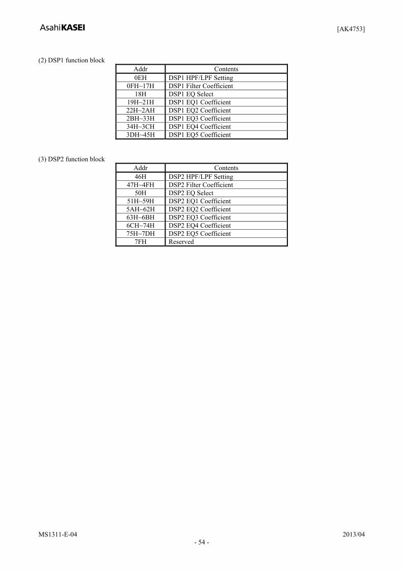
[AK4753]
MS1311-E-04 2013/04 - 54 -
(2) DSP1 function block
Addr Contents 0EH DSP1 HPF/LPF Setting
0FH~17H DSP1 Filter Coefficient 18H DSP1 EQ Select
19H~21H DSP1 EQ1 Coefficient 22H~2AH DSP1 EQ2 Coefficient 2BH~33H DSP1 EQ3 Coefficient 34H~3CH DSP1 EQ4 Coefficient 3DH~45H DSP1 EQ5 Coefficient
(3) DSP2 function block
Addr Contents 46H DSP2 HPF/LPF Setting
47H~4FH DSP2 Filter Coefficient 50H DSP2 EQ Select
51H~59H DSP2 EQ1 Coefficient 5AH~62H DSP2 EQ2 Coefficient 63H~6BH DSP2 EQ3 Coefficient 6CH~74H DSP2 EQ4 Coefficient 75H~7DH DSP2 EQ5 Coefficient
7FH Reserved
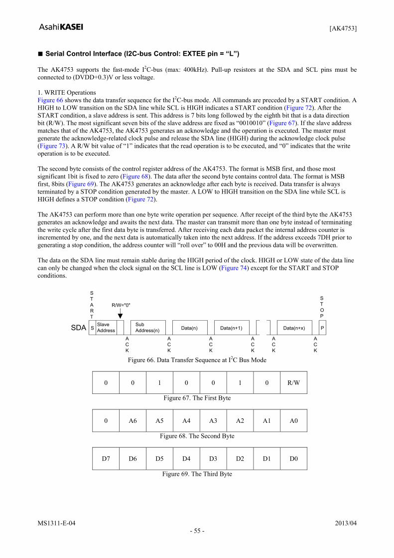
[AK4753]
MS1311-E-04 2013/04 - 55 -
Serial Control Interface (I2C-bus Control: EXTEE pin = “L”) The AK4753 supports the fast-mode I2C-bus (max: 400kHz). Pull-up resistors at the SDA and SCL pins must be connected to (DVDD+0.3)V or less voltage. 1. WRITE Operations Figure 66 shows the data transfer sequence for the I2C-bus mode. All commands are preceded by a START condition. A HIGH to LOW transition on the SDA line while SCL is HIGH indicates a START condition (Figure 72). After the START condition, a slave address is sent. This address is 7 bits long followed by the eighth bit that is a data direction bit (R/W). The most significant seven bits of the slave address are fixed as “0010010” (Figure 67). If the slave address matches that of the AK4753, the AK4753 generates an acknowledge and the operation is executed. The master must generate the acknowledge-related clock pulse and release the SDA line (HIGH) during the acknowledge clock pulse (Figure 73). A R/W bit value of “1” indicates that the read operation is to be executed, and “0” indicates that the write operation is to be executed. The second byte consists of the control register address of the AK4753. The format is MSB first, and those most significant 1bit is fixed to zero (Figure 68). The data after the second byte contains control data. The format is MSB first, 8bits (Figure 69). The AK4753 generates an acknowledge after each byte is received. Data transfer is always terminated by a STOP condition generated by the master. A LOW to HIGH transition on the SDA line while SCL is HIGH defines a STOP condition (Figure 72). The AK4753 can perform more than one byte write operation per sequence. After receipt of the third byte the AK4753 generates an acknowledge and awaits the next data. The master can transmit more than one byte instead of terminating the write cycle after the first data byte is transferred. After receiving each data packet the internal address counter is incremented by one, and the next data is automatically taken into the next address. If the address exceeds 7DH prior to generating a stop condition, the address counter will “roll over” to 00H and the previous data will be overwritten. The data on the SDA line must remain stable during the HIGH period of the clock. HIGH or LOW state of the data line can only be changed when the clock signal on the SCL line is LOW (Figure 74) except for the START and STOP conditions.
SDA SlaveAddressS
START
R/W="0"
ACK
SubAddress(n)
ACK
Data(n)
ACK
Data(n+1)
ACK
ACK
Data(n+x)
ACK
P
STOP
Figure 66. Data Transfer Sequence at I2C Bus Mode
0 0 1 0 0 1 0 R/W
Figure 67. The First Byte
0 A6 A5 A4 A3 A2 A1 A0
Figure 68. The Second Byte
D7 D6 D5 D4 D3 D2 D1 D0
Figure 69. The Third Byte
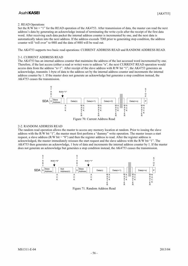
[AK4753]
MS1311-E-04 2013/04 - 56 -
2. READ Operations Set the R/W bit = “1” for the READ operation of the AK4753. After transmission of data, the master can read the next address’s data by generating an acknowledge instead of terminating the write cycle after the receipt of the first data word. After receiving each data packet the internal address counter is incremented by one, and the next data is automatically taken into the next address. If the address exceeds 7DH prior to generating stop condition, the address counter will “roll over” to 00H and the data of 00H will be read out. The AK4753 supports two basic read operations: CURRENT ADDRESS READ and RANDOM ADDRESS READ. 2-1. CURRENT ADDRESS READ The AK4753 has an internal address counter that maintains the address of the last accessed word incremented by one. Therefore, if the last access (either a read or write) were to address “n”, the next CURRENT READ operation would access data from the address “n+1”. After receipt of the slave address with R/W bit “1”, the AK4753 generates an acknowledge, transmits 1-byte of data to the address set by the internal address counter and increments the internal address counter by 1. If the master does not generate an acknowledge but generates a stop condition instead, the AK4753 ceases the transmission.
SDA SlaveAddressS
START
R/W="1"
ACK
ACK
Data(n+1)
ACK
Data(n+2)
ACK
ACK
Data(n+x)
NACK
P
STOP
Data(n)
MASTER
MASTER
MASTER
MASTER
MASTER
Figure 70. Current Address Read 2-2. RANDOM ADDRESS READ The random read operation allows the master to access any memory location at random. Prior to issuing the slave address with the R/W bit “1”, the master must first perform a “dummy” write operation. The master issues a start request, a slave address (R/W bit = “0”) and then the register address to read. After the register address is acknowledged, the master immediately reissues the start request and the slave address with the R/W bit “1”. The AK4753 then generates an acknowledge, 1 byte of data and increments the internal address counter by 1. If the master does not generate an acknowledge but generates a stop condition instead, the AK4753 ceases the transmission.
SDA SlaveAddressS
START
R/W="0"
ACK
ACK
ACK
Data(n)
ACK
Data(n+x)
ACK
P
STOP
SubAddress(n) S
SlaveAddress
R/W="1"
START
Data(n+1)
ACK
NACK
MASTER
MASTER
MASTER
MASTER
Figure 71. Random Address Read
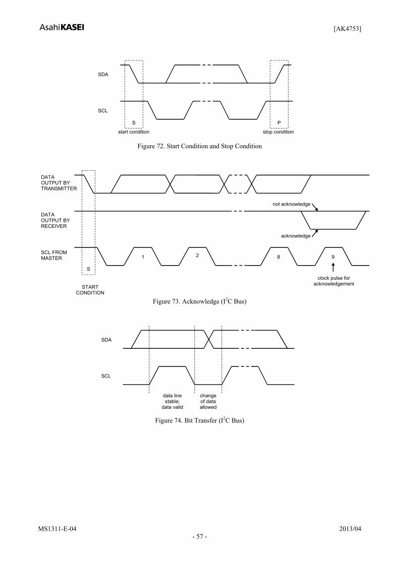
[AK4753]
MS1311-E-04 2013/04 - 57 -
SCL
SDA
stop conditionstart condition
S P
Figure 72. Start Condition and Stop Condition
SCL FROMMASTER
acknowledge
DATAOUTPUT BYTRANSMITTER
DATAOUTPUT BYRECEIVER
1 98
STARTCONDITION
not acknowledge
clock pulse foracknowledgement
S
2
Figure 73. Acknowledge (I2C Bus)
SCL
SDA
data linestable;
data valid
changeof dataallowed
Figure 74. Bit Transfer (I2C Bus)
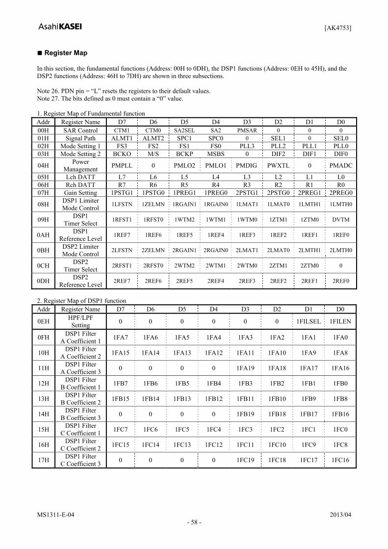
[AK4753]
MS1311-E-04 2013/04 - 58 -
Register Map In this section, the fundamental functions (Address: 00H to 0DH), the DSP1 functions (Address: 0EH to 45H), and the DSP2 functions (Address: 46H to 7DH) are shown in three subsections. Note 26. PDN pin = “L” resets the registers to their default values. Note 27. The bits defined as 0 must contain a “0” value. 1. Register Map of Fundamental function Addr Register Name D7 D6 D5 D4 D3 D2 D1 D0 00H SAR Control CTM1 CTM0 SA2SEL SA2 PMSAR 0 0 0 01H Signal Path ALMT1 ALMT2 SPC1 SPC0 0 SEL1 0 SEL0 02H Mode Setting 1 FS3 FS2 FS1 FS0 PLL3 PLL2 PLL1 PLL0 03H Mode Setting 2 BCKO M/S BCKP MSBS 0 DIF2 DIF1 DIF0
04H Power Management PMPLL 0 PMLO2 PMLO1 PMDIG PWXTL 0 PMADC
05H Lch DATT L7 L6 L5 L4 L3 L2 L1 L0 06H Rch DATT R7 R6 R5 R4 R3 R2 R1 R0 07H Gain Setting 1PSTG1 1PSTG0 1PREG1 1PREG0 2PSTG1 2PSTG0 2PREG1 2PREG0
08H DSP1 Limiter Mode Control 1LFSTN 1ZELMN 1RGAIN1 1RGAIN0 1LMAT1 1LMAT0 1LMTH1 1LMTH0
09H DSP1 Timer Select 1RFST1 1RFST0 1WTM2 1WTM1 1WTM0 1ZTM1 1ZTM0 DVTM
0AH DSP1 Reference Level 1REF7 1REF6 1REF5 1REF4 1REF3 1REF2 1REF1 1REF0
0BH DSP2 Limiter Mode Control 2LFSTN 2ZELMN 2RGAIN1 2RGAIN0 2LMAT1 2LMAT0 2LMTH1 2LMTH0
0CH DSP2 Timer Select 2RFST1 2RFST0 2WTM2 2WTM1 2WTM0 2ZTM1 2ZTM0 0
0DH DSP2 Reference Level 2REF7 2REF6 2REF5 2REF4 2REF3 2REF2 2REF1 2REF0
2. Register Map of DSP1 function Addr Register Name D7 D6 D5 D4 D3 D2 D1 D0
0EH HPF/LPF Setting 0 0 0 0 0 0 1FILSEL 1FILEN
0FH DSP1 Filter A Coefficient 1 1FA7 1FA6 1FA5 1FA4 1FA3 1FA2 1FA1 1FA0
10H DSP1 Filter A Coefficient 2 1FA15 1FA14 1FA13 1FA12 1FA11 1FA10 1FA9 1FA8
11H DSP1 Filter A Coefficient 3 0 0 0 0 1FA19 1FA18 1FA17 1FA16
12H DSP1 Filter B Coefficient 1 1FB7 1FB6 1FB5 1FB4 1FB3 1FB2 1FB1 1FB0
13H DSP1 Filter B Coefficient 2 1FB15 1FB14 1FB13 1FB12 1FB11 1FB10 1FB9 1FB8
14H DSP1 Filter B Coefficient 3 0 0 0 0 1FB19 1FB18 1FB17 1FB16
15H DSP1 Filter C Coefficient 1 1FC7 1FC6 1FC5 1FC4 1FC3 1FC2 1FC1 1FC0
16H DSP1 Filter C Coefficient 2 1FC15 1FC14 1FC13 1FC12 1FC11 1FC10 1FC9 1FC8
17H DSP1 Filter C Coefficient 3 0 0 0 0 1FC19 1FC18 1FC17 1FC16

[AK4753]
MS1311-E-04 2013/04 - 59 -
Addr Register Name D7 D6 D5 D4 D3 D2 D1 D0 18H DSP1 EQ Select 0 0 0 1EQ5 1EQ4 1EQ3 1EQ2 1EQ1
19H DSP1 EQ1 A Coefficient 1 1E1A7 1E1A6 1E1A5 1E1A4 1E1A3 1E1A2 1E1A1 1E1A0
1AH DSP1 EQ1 A Coefficient 2 1E1A15 1E1A14 1E1A13 1E1A12 1E1A11 1E1A10 1E1A9 1E1A8
1BH DSP1 EQ1 A Coefficient 3 0 0 0 0 1E1A19 1E1A18 1E1A17 1E1A16
1CH DSP1 EQ1 B Coefficient 1 1E1B7 1E1B6 1E1B5 1E1B4 1E1B3 1E1B2 1E1B1 1E1B0
1DH DSP1 EQ1 B Coefficient 2 1E1B15 1E1B14 1E1B13 1E1B12 1E1B11 1E1B10 1E1B9 1E1B8
1EH DSP1 EQ1 B Coefficient 3 0 0 0 0 1E1B19 1E1B18 1E1B17 1E1B16
1FH DSP1 EQ1 C Coefficient 1 1E1C7 1E1C6 1E1C5 1E1C4 1E1C3 1E1C2 1E1C1 1E1C0
20H DSP1 EQ1 C Coefficient 2 1E1C15 1E1C14 1E1C13 1E1C12 1E1C11 1E1C10 1E1C9 1E1C8
21H DSP1 EQ1 C Coefficient 3 0 0 0 0 1E1C19 1E1C18 1E1C17 1E1C16
22H DSP1 EQ2 A Coefficient 1 1E2A7 1E2A6 1E2A5 1E2A4 1E2A3 1E2A2 1E2A1 1E2A0
23H DSP1 EQ2 A Coefficient 2 1E2A15 1E2A14 1E2A13 1E2A12 1E2A11 1E2A10 1E2A9 1E2A8
24H DSP1 EQ2 A Coefficient 3 0 0 0 0 1E2A19 1E2A18 1E2A17 1E2A16
25H DSP1 EQ2 B Coefficient 1 1E2B7 1E2B6 1E2B5 1E2B4 1E2B3 1E2B2 1E2B1 1E2B0
26H DSP1 EQ2 B Coefficient 2 1E2B15 1E2B14 1E2B13 1E2B12 1E2B11 1E2B10 1E2B9 1E2B8
27H DSP1 EQ2 B Coefficient 3 0 0 0 0 1E2B19 1E2B18 1E2B17 1E2B16
28H DSP1 EQ2 C Coefficient 1 1E2C7 1E2C6 1E2C5 1E2C4 1E2C3 1E2C2 1E2C1 1E2C0
29H DSP1 EQ2 C Coefficient 2 1E2C15 1E2C14 1E2C13 1E2C12 1E2C11 1E2C10 1E2C9 1E2C8
2AH DSP1 EQ2 C Coefficient 3 0 0 0 0 1E2C19 1E2C18 1E2C17 1E2C16
2BH DSP1 EQ3 A Coefficient 1 1E3A7 1E3A6 1E3A5 1E3A4 1E3A3 1E3A2 1E3A1 1E3A0
2CH DSP1 EQ3 A Coefficient 2 1E3A15 1E3A14 1E3A13 1E3A12 1E3A11 1E3A10 1E3A9 1E3A8
2DH DSP1 EQ3 A Coefficient 3 0 0 0 0 1E3A19 1E3A18 1E3A17 1E3A16
2EH DSP1 EQ3 B Coefficient 1 1E3B7 1E3B6 1E3B5 1E3B4 1E3B3 1E3B2 1E3B1 1E3B0
2FH DSP1 EQ3 B Coefficient 2 1E3B15 1E3B14 1E3B13 1E3B12 1E3B11 1E3B10 1E3B9 1E3B8
30H DSP1 EQ3 B Coefficient 3 0 0 0 0 1E3B19 1E3B18 1E3B17 1E3B16
31H DSP1 EQ3 C Coefficient 1 1E3C7 1E3C6 1E3C5 1E3C4 1E3C3 1E3C2 1E3C1 1E3C0
32H DSP1 EQ3 C Coefficient 2 1E3C15 1E3C14 1E3C13 1E3C12 1E3C11 1E3C10 1E3C9 1E3C8
33H DSP1 EQ3 C Coefficient 3 0 0 0 0 1E3C19 1E3C18 1E3C17 1E3C16

[AK4753]
MS1311-E-04 2013/04 - 60 -
Addr Register Name D7 D6 D5 D4 D3 D2 D1 D0
34H DSP1 EQ4 A Coefficient 1 1E4A7 1E4A6 1E4A5 1E4A4 1E4A3 1E4A2 1E4A1 1E4A0
35H DSP1 EQ4 A Coefficient 2 1E4A15 1E4A14 1E4A13 1E4A12 1E4A11 1E4A10 1E4A9 1E4A8
36H DSP1 EQ4 A Coefficient 3 0 0 0 0 1E4A19 1E4A18 1E4A17 1E4A16
37H DSP1 EQ4 B Coefficient 1 1E4B7 1E4B6 1E4B5 1E4B4 1E4B3 1E4B2 1E4B1 1E4B0
38H DSP1 EQ4 B Coefficient 2 1E4B15 1E4B14 1E4B13 1E4B12 1E4B11 1E4B10 1E4B9 1E4B8
39H DSP1 EQ4 B Coefficient 3 0 0 0 0 1E4B19 1E4B18 1E4B17 1E4B16
3AH DSP1 EQ4 C Coefficient 1 1E4C7 1E4C6 1E4C5 1E4C4 1E4C3 1E4C2 1E4C1 1E4C0
3BH DSP1 EQ4 C Coefficient 2 1E4C15 1E4C14 1E4C13 1E4C12 1E4C11 1E4C10 1E4C9 1E4C8
3CH DSP1 EQ4 C Coefficient 3 0 0 0 0 1E4C19 1E4C18 1E4C17 1E4C16
3DH DSP1 EQ5 A Coefficient 1 1E5A7 1E5A6 1E5A5 1E5A4 1E5A3 1E5A2 1E5A1 1E5A0
3EH DSP1 EQ5 A Coefficient 2 1E5A15 1E5A14 1E5A13 1E5A12 1E5A11 1E5A10 1E5A9 1E5A8
3FH DSP1 EQ5 A Coefficient 3 0 0 0 0 1E5A19 1E5A18 1E5A17 1E5A16
40H DSP1 EQ5 B Coefficient 1 1E5B7 1E5B6 1E5B5 1E5B4 1E5B3 1E5B2 1E5B1 1E5B0
41H DSP1 EQ5 B Coefficient 2 1E5B15 1E5B14 1E5B13 1E5B12 1E5B11 1E5B10 1E5B9 1E5B8
42H DSP1 EQ5 B Coefficient 3 0 0 0 0 1E5B19 1E5B18 1E5B17 1E5B16
43H DSP1 EQ5 C Coefficient 1 1E5C7 1E5C6 1E5C5 1E5C4 1E5C3 1E5C2 1E5C1 1E5C0
44H DSP1 EQ5 C Coefficient 2 1E5C15 1E5C14 1E5C13 1E5C12 1E5C11 1E5C10 1E5C9 1E5C8
45H DSP1 EQ5 C Coefficient 3 0 0 0 0 1E5C19 1E5C18 1E5C17 1E5C16
3. Register Map of DSP2 function Addr Register Name D7 D6 D5 D4 D3 D2 D1 D0
46H HPF/LPF Setting 0 0 0 0 0 0 2FILSEL 2FILEN
47H DSP2 Filter A Coefficient 1 2FA7 2FA6 2FA5 2FA4 2FA3 2FA2 2FA1 2FA0
48H DSP2 Filter A Coefficient 2 2FA15 2FA14 2FA13 2FA12 2FA11 2FA10 2FA9 2FA8
49H DSP2 Filter A Coefficient 3 0 0 0 0 2FA19 2FA18 2FA17 2FA16
4AH DSP2 Filter B Coefficient 1 2FB7 2FB6 2FB5 2FB4 2FB3 2FB2 2FB1 2FB0
4BH DSP2 Filter B Coefficient 2 2FB15 2FB14 2FB13 2FB12 2FB11 2FB10 2FB9 2FB8
4CH DSP2 Filter B Coefficient 3 0 0 0 0 2FB19 2FB18 2FB17 2FB16
4DH DSP2 Filter C Coefficient 1 2FC7 2FC6 2FC5 2FC4 2FC3 2FC2 2FC1 2FC0

[AK4753]
MS1311-E-04 2013/04 - 61 -
Addr Register Name D7 D6 D5 D4 D3 D2 D1 D0
4EH DSP2 Filter C Coefficient 2 2FC15 2FC14 2FC13 2FC12 2FC11 2FC10 2FC9 2FC8
4FH DSP2 Filter C Coefficient 3 0 0 0 0 2FC19 2FC18 2FC17 2FC16
50H DSP2 EQ Select 0 0 0 2EQ5 2EQ4 2EQ3 2EQ2 2EQ1
51H DSP2 EQ1 A Coefficient 1 2E1A7 2E1A6 2E1A5 2E1A4 2E1A3 2E1A2 2E1A1 2E1A0
52H DSP2 EQ1 A Coefficient 2 2E1A15 2E1A14 2E1A13 2E1A12 2E1A11 2E1A10 2E1A9 2E1A8
53H DSP2 EQ1 A Coefficient 3 0 0 0 0 2E1A19 2E1A18 2E1A17 2E1A16
54H DSP2 EQ1 B Coefficient 1 2E1B7 2E1B6 2E1B5 2E1B4 2E1B3 2E1B2 2E1B1 2E1B0
55H DSP2 EQ1 B Coefficient 2 2E1B15 2E1B14 2E1B13 2E1B12 2E1B11 2E1B10 2E1B9 2E1B8
56H DSP2 EQ1 B Coefficient 3 0 0 0 0 2E1B19 2E1B18 2E1B17 2E1B16
57H DSP2 EQ1 C Coefficient 1 2E1C7 2E1C6 2E1C5 2E1C4 2E1C3 2E1C2 2E1C1 2E1C0
58H DSP2 EQ1 C Coefficient 2 2E1C15 2E1C14 2E1C13 2E1C12 2E1C11 2E1C10 2E1C9 2E1C8
59H DSP2 EQ1 C Coefficient 3 0 0 0 0 2E1C19 2E1C18 2E1C17 2E1C16
5AH DSP2 EQ2 A Coefficient 1 2E2A7 2E2A6 2E2A5 2E2A4 2E2A3 2E2A2 2E2A1 2E2A0
5BH DSP2 EQ2 A Coefficient 2 2E2A15 2E2A14 2E2A13 2E2A12 2E2A11 2E2A10 2E2A9 2E2A8
5CH DSP2 EQ2 A Coefficient 3 0 0 0 0 2E2A19 2E2A18 2E2A17 2E2A16
5DH DSP2 EQ2 B Coefficient 1 2E2B7 2E2B6 2E2B5 2E2B4 2E2B3 2E2B2 2E2B1 2E2B0
5EH DSP2 EQ2 B Coefficient 2 2E2B15 2E2B14 2E2B13 2E2B12 2E2B11 2E2B10 2E2B9 2E2B8
5FH DSP2 EQ2 B Coefficient 3 0 0 0 0 2E2B19 2E2B18 2E2B17 2E2B16
60H DSP2 EQ2 C Coefficient 1 2E2C7 2E2C6 2E2C5 2E2C4 2E2C3 2E2C2 2E2C1 2E2C0
61H DSP2 EQ2 C Coefficient 2 2E2C15 2E2C14 2E2C13 2E2C12 2E2C11 2E2C10 2E2C9 2E2C8
62H DSP2 EQ2 C Coefficient 3 0 0 0 0 2E2C19 2E2C18 2E2C17 2E2C16
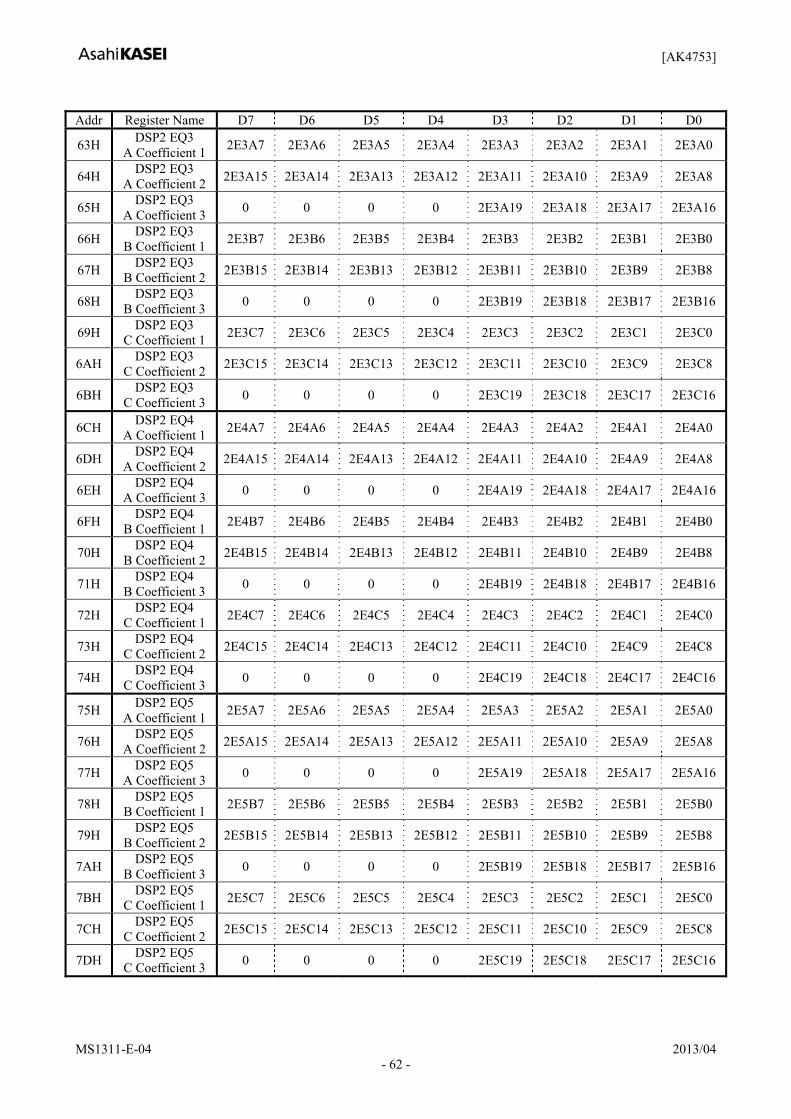
[AK4753]
MS1311-E-04 2013/04 - 62 -
Addr Register Name D7 D6 D5 D4 D3 D2 D1 D0
63H DSP2 EQ3 A Coefficient 1 2E3A7 2E3A6 2E3A5 2E3A4 2E3A3 2E3A2 2E3A1 2E3A0
64H DSP2 EQ3 A Coefficient 2 2E3A15 2E3A14 2E3A13 2E3A12 2E3A11 2E3A10 2E3A9 2E3A8
65H DSP2 EQ3 A Coefficient 3 0 0 0 0 2E3A19 2E3A18 2E3A17 2E3A16
66H DSP2 EQ3 B Coefficient 1 2E3B7 2E3B6 2E3B5 2E3B4 2E3B3 2E3B2 2E3B1 2E3B0
67H DSP2 EQ3 B Coefficient 2 2E3B15 2E3B14 2E3B13 2E3B12 2E3B11 2E3B10 2E3B9 2E3B8
68H DSP2 EQ3 B Coefficient 3 0 0 0 0 2E3B19 2E3B18 2E3B17 2E3B16
69H DSP2 EQ3 C Coefficient 1 2E3C7 2E3C6 2E3C5 2E3C4 2E3C3 2E3C2 2E3C1 2E3C0
6AH DSP2 EQ3 C Coefficient 2 2E3C15 2E3C14 2E3C13 2E3C12 2E3C11 2E3C10 2E3C9 2E3C8
6BH DSP2 EQ3 C Coefficient 3 0 0 0 0 2E3C19 2E3C18 2E3C17 2E3C16
6CH DSP2 EQ4 A Coefficient 1 2E4A7 2E4A6 2E4A5 2E4A4 2E4A3 2E4A2 2E4A1 2E4A0
6DH DSP2 EQ4 A Coefficient 2 2E4A15 2E4A14 2E4A13 2E4A12 2E4A11 2E4A10 2E4A9 2E4A8
6EH DSP2 EQ4 A Coefficient 3 0 0 0 0 2E4A19 2E4A18 2E4A17 2E4A16
6FH DSP2 EQ4 B Coefficient 1 2E4B7 2E4B6 2E4B5 2E4B4 2E4B3 2E4B2 2E4B1 2E4B0
70H DSP2 EQ4 B Coefficient 2 2E4B15 2E4B14 2E4B13 2E4B12 2E4B11 2E4B10 2E4B9 2E4B8
71H DSP2 EQ4 B Coefficient 3 0 0 0 0 2E4B19 2E4B18 2E4B17 2E4B16
72H DSP2 EQ4 C Coefficient 1 2E4C7 2E4C6 2E4C5 2E4C4 2E4C3 2E4C2 2E4C1 2E4C0
73H DSP2 EQ4 C Coefficient 2 2E4C15 2E4C14 2E4C13 2E4C12 2E4C11 2E4C10 2E4C9 2E4C8
74H DSP2 EQ4 C Coefficient 3 0 0 0 0 2E4C19 2E4C18 2E4C17 2E4C16
75H DSP2 EQ5 A Coefficient 1 2E5A7 2E5A6 2E5A5 2E5A4 2E5A3 2E5A2 2E5A1 2E5A0
76H DSP2 EQ5 A Coefficient 2 2E5A15 2E5A14 2E5A13 2E5A12 2E5A11 2E5A10 2E5A9 2E5A8
77H DSP2 EQ5 A Coefficient 3 0 0 0 0 2E5A19 2E5A18 2E5A17 2E5A16
78H DSP2 EQ5 B Coefficient 1 2E5B7 2E5B6 2E5B5 2E5B4 2E5B3 2E5B2 2E5B1 2E5B0
79H DSP2 EQ5 B Coefficient 2 2E5B15 2E5B14 2E5B13 2E5B12 2E5B11 2E5B10 2E5B9 2E5B8
7AH DSP2 EQ5 B Coefficient 3 0 0 0 0 2E5B19 2E5B18 2E5B17 2E5B16
7BH DSP2 EQ5 C Coefficient 1 2E5C7 2E5C6 2E5C5 2E5C4 2E5C3 2E5C2 2E5C1 2E5C0
7CH DSP2 EQ5 C Coefficient 2 2E5C15 2E5C14 2E5C13 2E5C12 2E5C11 2E5C10 2E5C9 2E5C8
7DH DSP2 EQ5 C Coefficient 3 0 0 0 0 2E5C19 2E5C18 2E5C17 2E5C16
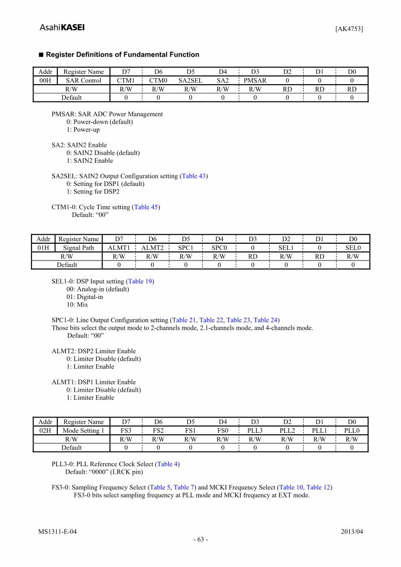
[AK4753]
MS1311-E-04 2013/04 - 63 -
Register Definitions of Fundamental Function Addr Register Name D7 D6 D5 D4 D3 D2 D1 D0 00H SAR Control CTM1 CTM0 SA2SEL SA2 PMSAR 0 0 0
R/W R/W R/W R/W R/W R/W RD RD RD Default 0 0 0 0 0 0 0 0
PMSAR: SAR ADC Power Management
0: Power-down (default) 1: Power-up
SA2: SAIN2 Enable
0: SAIN2 Disable (default) 1: SAIN2 Enable
SA2SEL: SAIN2 Output Configuration setting (Table 43)
0: Setting for DSP1 (default) 1: Setting for DSP2
CTM1-0: Cycle Time setting (Table 45)
Default: “00”
Addr Register Name D7 D6 D5 D4 D3 D2 D1 D0 01H Signal Path ALMT1 ALMT2 SPC1 SPC0 0 SEL1 0 SEL0
R/W R/W R/W R/W R/W RD R/W RD R/W Default 0 0 0 0 0 0 0 0
SEL1-0: DSP Input setting (Table 19)
00: Analog-in (default) 01: Digital-in 10: Mix
SPC1-0: Line Output Configuration setting (Table 21, Table 22, Table 23, Table 24) Those bits select the output mode to 2-channels mode, 2.1-channels mode, and 4-channels mode.
Default: “00”
ALMT2: DSP2 Limiter Enable 0: Limiter Disable (default) 1: Limiter Enable
ALMT1: DSP1 Limiter Enable
0: Limiter Disable (default) 1: Limiter Enable
Addr Register Name D7 D6 D5 D4 D3 D2 D1 D0 02H Mode Setting 1 FS3 FS2 FS1 FS0 PLL3 PLL2 PLL1 PLL0
R/W R/W R/W R/W R/W R/W R/W R/W R/W Default 0 0 0 0 0 0 0 0
PLL3-0: PLL Reference Clock Select (Table 4)
Default: “0000” (LRCK pin)
FS3-0: Sampling Frequency Select (Table 5, Table 7) and MCKI Frequency Select (Table 10, Table 12) FS3-0 bits select sampling frequency at PLL mode and MCKI frequency at EXT mode.

[AK4753]
MS1311-E-04 2013/04 - 64 -
Addr Register Name D7 D6 D5 D4 D3 D2 D1 D0 03H Mode Setting 2 BCKO M/S BCKP MSBS 0 DIF2 DIF1 DIF0
R/W R/W R/W R/W R/W RD R/W R/W R/W Default 1 0 0 0 0 0 1 1
DIF2-0: Audio Interface Format (Table 15)
Default: “011” (I2S)
MSBS: LRCK Polarity at DSP Mode (Table 16, Table 17, Table 18) 0: The rising edge (“↑”) of LRCK is half clock of BICK before the channel change. (default) 1: The rising edge (“↑”) of LRCK is one clock of BICK before the channel change.
BCKP: BICK Polarity at DSP Mode (Table 16, Table 17, Table 18)
0: SDTI is latched by the falling edge (“↓”) of BICK. (default) 1: SDTI is latched by the rising edge (“↑”) of BICK.
M/S: Master / Slave Mode Setting 0: Slave Mode (default) 1: Master Mode
BCKO: BICK Output Frequency Select at Master Mode (Table 9)
Addr Register Name D7 D6 D5 D4 D3 D2 D1 D0
04H Power Management PMPLL 0 PMLO2 PMLO1 PMDIG PWXTL 0 PMADC
R/W R/W RD R/W R/W R/W R/W RD R/W Default 0 0 0 0 0 0 0 0
PMADC: ADC Power Management
0: Power-down (default) 1: Power-up
PWXTL: The power management of the crystal oscillation circuit
0: Power OFF (default) 1: Power ON
PMDIG: DSP & DAC Digital Power Management
0: Power-down (default) 1: Power-up
PMLO1: Line Out1 Power Management and External Mute Control
0: Power-down (default) 1: Power-up
PMLO2: Line Out2 Power Management and External Mute Control
0: Power-down (default) 1: Power-up
PMPLL: PLL Power Management
0: EXT Mode and Power-Down (default) 1: PLL Mode and Power-up
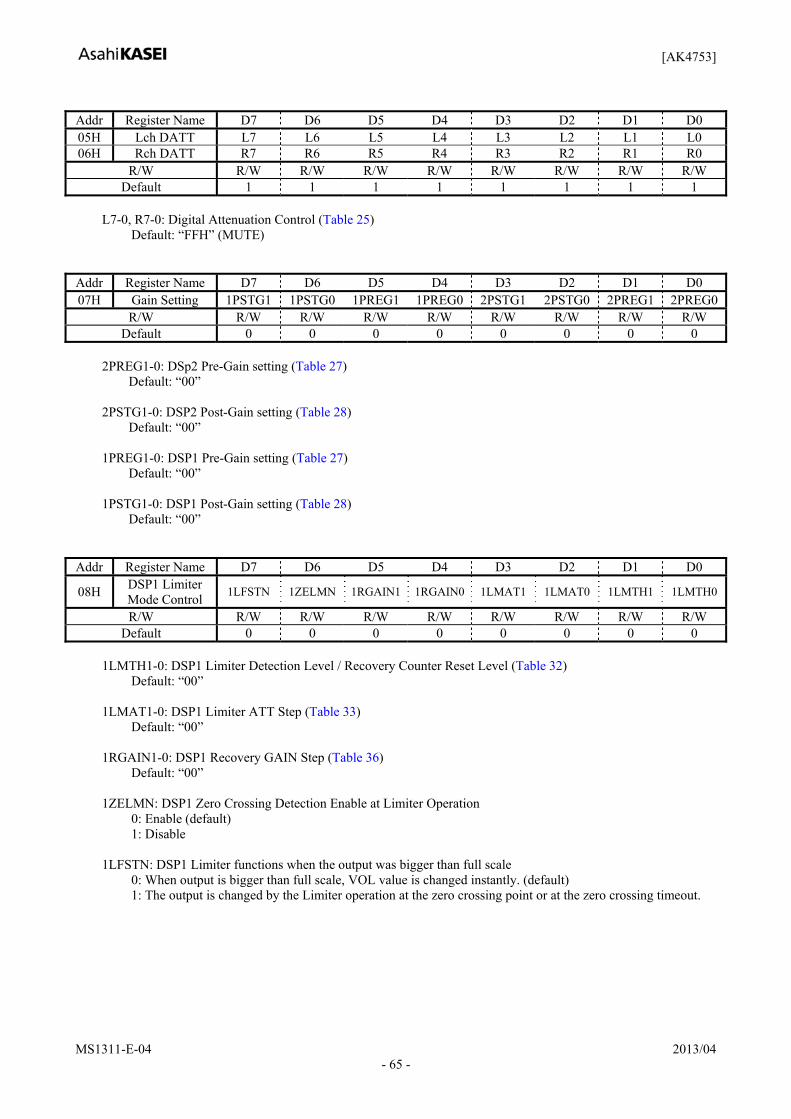
[AK4753]
MS1311-E-04 2013/04 - 65 -
Addr Register Name D7 D6 D5 D4 D3 D2 D1 D0 05H Lch DATT L7 L6 L5 L4 L3 L2 L1 L0 06H Rch DATT R7 R6 R5 R4 R3 R2 R1 R0
R/W R/W R/W R/W R/W R/W R/W R/W R/W Default 1 1 1 1 1 1 1 1
L7-0, R7-0: Digital Attenuation Control (Table 25)
Default: “FFH” (MUTE) Addr Register Name D7 D6 D5 D4 D3 D2 D1 D0 07H Gain Setting 1PSTG1 1PSTG0 1PREG1 1PREG0 2PSTG1 2PSTG0 2PREG1 2PREG0
R/W R/W R/W R/W R/W R/W R/W R/W R/W Default 0 0 0 0 0 0 0 0
2PREG1-0: DSp2 Pre-Gain setting (Table 27)
Default: “00”
2PSTG1-0: DSP2 Post-Gain setting (Table 28) Default: “00”
1PREG1-0: DSP1 Pre-Gain setting (Table 27)
Default: “00”
1PSTG1-0: DSP1 Post-Gain setting (Table 28) Default: “00”
Addr Register Name D7 D6 D5 D4 D3 D2 D1 D0
08H DSP1 Limiter Mode Control 1LFSTN 1ZELMN 1RGAIN1 1RGAIN0 1LMAT1 1LMAT0 1LMTH1 1LMTH0
R/W R/W R/W R/W R/W R/W R/W R/W R/W Default 0 0 0 0 0 0 0 0
1LMTH1-0: DSP1 Limiter Detection Level / Recovery Counter Reset Level (Table 32)
Default: “00”
1LMAT1-0: DSP1 Limiter ATT Step (Table 33) Default: “00”
1RGAIN1-0: DSP1 Recovery GAIN Step (Table 36)
Default: “00”
1ZELMN: DSP1 Zero Crossing Detection Enable at Limiter Operation 0: Enable (default) 1: Disable
1LFSTN: DSP1 Limiter functions when the output was bigger than full scale
0: When output is bigger than full scale, VOL value is changed instantly. (default) 1: The output is changed by the Limiter operation at the zero crossing point or at the zero crossing timeout.
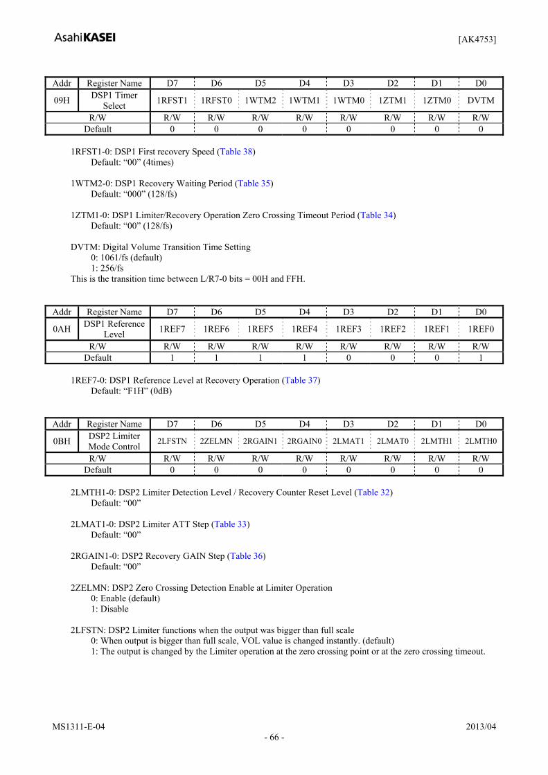
[AK4753]
MS1311-E-04 2013/04 - 66 -
Addr Register Name D7 D6 D5 D4 D3 D2 D1 D0
09H DSP1 Timer Select 1RFST1 1RFST0 1WTM2 1WTM1 1WTM0 1ZTM1 1ZTM0 DVTM
R/W R/W R/W R/W R/W R/W R/W R/W R/W Default 0 0 0 0 0 0 0 0
1RFST1-0: DSP1 First recovery Speed (Table 38)
Default: “00” (4times)
1WTM2-0: DSP1 Recovery Waiting Period (Table 35) Default: “000” (128/fs)
1ZTM1-0: DSP1 Limiter/Recovery Operation Zero Crossing Timeout Period (Table 34)
Default: “00” (128/fs)
DVTM: Digital Volume Transition Time Setting 0: 1061/fs (default) 1: 256/fs
This is the transition time between L/R7-0 bits = 00H and FFH. Addr Register Name D7 D6 D5 D4 D3 D2 D1 D0
0AH DSP1 Reference Level 1REF7 1REF6 1REF5 1REF4 1REF3 1REF2 1REF1 1REF0
R/W R/W R/W R/W R/W R/W R/W R/W R/W Default 1 1 1 1 0 0 0 1
1REF7-0: DSP1 Reference Level at Recovery Operation (Table 37)
Default: “F1H” (0dB) Addr Register Name D7 D6 D5 D4 D3 D2 D1 D0
0BH DSP2 Limiter Mode Control 2LFSTN 2ZELMN 2RGAIN1 2RGAIN0 2LMAT1 2LMAT0 2LMTH1 2LMTH0
R/W R/W R/W R/W R/W R/W R/W R/W R/W Default 0 0 0 0 0 0 0 0
2LMTH1-0: DSP2 Limiter Detection Level / Recovery Counter Reset Level (Table 32)
Default: “00”
2LMAT1-0: DSP2 Limiter ATT Step (Table 33) Default: “00”
2RGAIN1-0: DSP2 Recovery GAIN Step (Table 36)
Default: “00”
2ZELMN: DSP2 Zero Crossing Detection Enable at Limiter Operation 0: Enable (default) 1: Disable
2LFSTN: DSP2 Limiter functions when the output was bigger than full scale
0: When output is bigger than full scale, VOL value is changed instantly. (default) 1: The output is changed by the Limiter operation at the zero crossing point or at the zero crossing timeout.
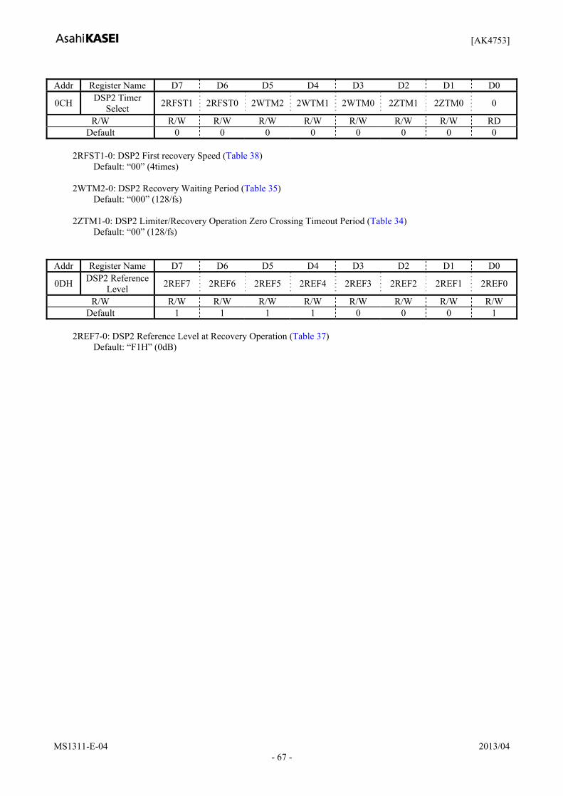
[AK4753]
MS1311-E-04 2013/04 - 67 -
Addr Register Name D7 D6 D5 D4 D3 D2 D1 D0
0CH DSP2 Timer Select 2RFST1 2RFST0 2WTM2 2WTM1 2WTM0 2ZTM1 2ZTM0 0
R/W R/W R/W R/W R/W R/W R/W R/W RD Default 0 0 0 0 0 0 0 0
2RFST1-0: DSP2 First recovery Speed (Table 38)
Default: “00” (4times)
2WTM2-0: DSP2 Recovery Waiting Period (Table 35) Default: “000” (128/fs)
2ZTM1-0: DSP2 Limiter/Recovery Operation Zero Crossing Timeout Period (Table 34)
Default: “00” (128/fs) Addr Register Name D7 D6 D5 D4 D3 D2 D1 D0
0DH DSP2 Reference Level 2REF7 2REF6 2REF5 2REF4 2REF3 2REF2 2REF1 2REF0
R/W R/W R/W R/W R/W R/W R/W R/W R/W Default 1 1 1 1 0 0 0 1
2REF7-0: DSP2 Reference Level at Recovery Operation (Table 37)
Default: “F1H” (0dB)
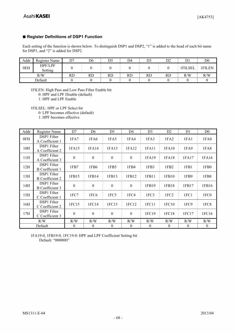
[AK4753]
MS1311-E-04 2013/04 - 68 -
Register Definitions of DSP1 Function Each setting of the function is shown below. To distinguish DSP1 and DSP2, “1” is added to the head of each bit name for DSP1, and “2” is added for DSP2. Addr Register Name D7 D6 D5 D4 D3 D2 D1 D0
0EH HPF/LPF Setting 0 0 0 0 0 0 1FILSEL 1FILEN
R/W RD RD RD RD RD RD R/W R/W Default 0 0 0 0 0 0 0 0
1FILEN: High Pass and Low Pass Filter Enable bit
0: HPF and LPF Disable (default) 1: HPF and LPF Enable
1FILSEL: HPF or LPF Select bit
0: LPF becomes effective (default) 1: HPF becomes effective
Addr Register Name D7 D6 D5 D4 D3 D2 D1 D0
0FH DSP1 Filter A Coefficient 1 1FA7 1FA6 1FA5 1FA4 1FA3 1FA2 1FA1 1FA0
10H DSP1 Filter A Coefficient 2 1FA15 1FA14 1FA13 1FA12 1FA11 1FA10 1FA9 1FA8
11H DSP1 Filter A Coefficient 3 0 0 0 0 1FA19 1FA18 1FA17 1FA16
12H DSP1 Filter B Coefficient 1 1FB7 1FB6 1FB5 1FB4 1FB3 1FB2 1FB1 1FB0
13H DSP1 Filter B Coefficient 2 1FB15 1FB14 1FB13 1FB12 1FB11 1FB10 1FB9 1FB8
14H DSP1 Filter B Coefficient 3 0 0 0 0 1FB19 1FB18 1FB17 1FB16
15H DSP1 Filter C Coefficient 1 1FC7 1FC6 1FC5 1FC4 1FC3 1FC2 1FC1 1FC0
16H DSP1 Filter C Coefficient 2 1FC15 1FC14 1FC13 1FC12 1FC11 1FC10 1FC9 1FC8
17H DSP1 Filter C Coefficient 3 0 0 0 0 1FC19 1FC18 1FC17 1FC16
R/W R/W R/W R/W R/W R/W R/W R/W R/W Default 0 0 0 0 0 0 0 0
1FA19-0, 1FB19-0, 1FC19-0: HPF and LPF Coefficient Setting bit
Default: “00000H”
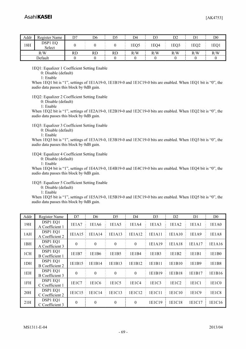
[AK4753]
MS1311-E-04 2013/04 - 69 -
Addr Register Name D7 D6 D5 D4 D3 D2 D1 D0
18H DSP1 EQ Select 0 0 0 1EQ5 1EQ4 1EQ3 1EQ2 1EQ1
R/W RD RD RD R/W R/W R/W R/W R/W Default 0 0 0 0 0 0 0 0
1EQ1: Equalizer 1 Coefficient Setting Enable
0: Disable (default) 1: Enable
When 1EQ1 bit is “1”, settings of 1E1A19-0, 1E1B19-0 and 1E1C19-0 bits are enabled. When 1EQ1 bit is “0”, the audio data passes this block by 0dB gain.
1EQ2: Equalizer 2 Coefficient Setting Enable
0: Disable (default) 1: Enable
When 1EQ2 bit is “1”, settings of 1E2A19-0, 1E2B19-0 and 1E2C19-0 bits are enabled. When 1EQ2 bit is “0”, the audio data passes this block by 0dB gain.
1EQ3: Equalizer 3 Coefficient Setting Enable
0: Disable (default) 1: Enable
When 1EQ3 bit is “1”, settings of 1E3A19-0, 1E3B19-0 and 1E3C19-0 bits are enabled. When 1EQ3 bit is “0”, the audio data passes this block by 0dB gain.
1EQ4: Equalizer 4 Coefficient Setting Enable
0: Disable (default) 1: Enable
When 1EQ4 bit is “1”, settings of 1E4A19-0, 1E4B19-0 and 1E4C19-0 bits are enabled. When 1EQ4 bit is “0”, the audio data passes this block by 0dB gain.
1EQ5: Equalizer 5 Coefficient Setting Enable
0: Disable (default) 1: Enable
When 1EQ5 bit is “1”, settings of 1E5A19-0, 1E5B19-0 and 1E5C19-0 bits are enabled. When 1EQ5 bit is “0”, the audio data passes this block by 0dB gain.
Addr Register Name D7 D6 D5 D4 D3 D2 D1 D0
19H DSP1 EQ1 A Coefficient 1 1E1A7 1E1A6 1E1A5 1E1A4 1E1A3 1E1A2 1E1A1 1E1A0
1AH DSP1 EQ1 A Coefficient 2 1E1A15 1E1A14 1E1A13 1E1A12 1E1A11 1E1A10 1E1A9 1E1A8
1BH DSP1 EQ1 A Coefficient 3 0 0 0 0 1E1A19 1E1A18 1E1A17 1E1A16
1CH DSP1 EQ1 B Coefficient 1 1E1B7 1E1B6 1E1B5 1E1B4 1E1B3 1E1B2 1E1B1 1E1B0
1DH DSP1 EQ1 B Coefficient 2 1E1B15 1E1B14 1E1B13 1E1B12 1E1B11 1E1B10 1E1B9 1E1B8
1EH DSP1 EQ1 B Coefficient 3 0 0 0 0 1E1B19 1E1B18 1E1B17 1E1B16
1FH DSP1 EQ1 C Coefficient 1 1E1C7 1E1C6 1E1C5 1E1C4 1E1C3 1E1C2 1E1C1 1E1C0
20H DSP1 EQ1 C Coefficient 2 1E1C15 1E1C14 1E1C13 1E1C12 1E1C11 1E1C10 1E1C9 1E1C8
21H DSP1 EQ1 C Coefficient 3 0 0 0 0 1E1C19 1E1C18 1E1C17 1E1C16
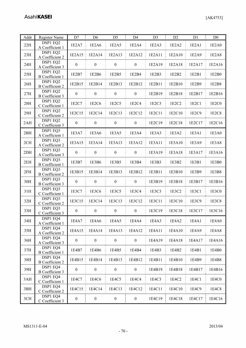
[AK4753]
MS1311-E-04 2013/04 - 70 -
Addr Register Name D7 D6 D5 D4 D3 D2 D1 D0
22H DSP1 EQ2 A Coefficient 1 1E2A7 1E2A6 1E2A5 1E2A4 1E2A3 1E2A2 1E2A1 1E2A0
23H DSP1 EQ2 A Coefficient 2 1E2A15 1E2A14 1E2A13 1E2A12 1E2A11 1E2A10 1E2A9 1E2A8
24H DSP1 EQ2 A Coefficient 3 0 0 0 0 1E2A19 1E2A18 1E2A17 1E2A16
25H DSP1 EQ2 B Coefficient 1 1E2B7 1E2B6 1E2B5 1E2B4 1E2B3 1E2B2 1E2B1 1E2B0
26H DSP1 EQ2 B Coefficient 2 1E2B15 1E2B14 1E2B13 1E2B12 1E2B11 1E2B10 1E2B9 1E2B8
27H DSP1 EQ2 B Coefficient 3 0 0 0 0 1E2B19 1E2B18 1E2B17 1E2B16
28H DSP1 EQ2 C Coefficient 1 1E2C7 1E2C6 1E2C5 1E2C4 1E2C3 1E2C2 1E2C1 1E2C0
29H DSP1 EQ2 C Coefficient 2 1E2C15 1E2C14 1E2C13 1E2C12 1E2C11 1E2C10 1E2C9 1E2C8
2AH DSP1 EQ2 C Coefficient 3 0 0 0 0 1E2C19 1E2C18 1E2C17 1E2C16
2BH DSP1 EQ3 A Coefficient 1 1E3A7 1E3A6 1E3A5 1E3A4 1E3A3 1E3A2 1E3A1 1E3A0
2CH DSP1 EQ3 A Coefficient 2 1E3A15 1E3A14 1E3A13 1E3A12 1E3A11 1E3A10 1E3A9 1E3A8
2DH DSP1 EQ3 A Coefficient 3 0 0 0 0 1E3A19 1E3A18 1E3A17 1E3A16
2EH DSP1 EQ3 B Coefficient 1 1E3B7 1E3B6 1E3B5 1E3B4 1E3B3 1E3B2 1E3B1 1E3B0
2FH DSP1 EQ3 B Coefficient 2 1E3B15 1E3B14 1E3B13 1E3B12 1E3B11 1E3B10 1E3B9 1E3B8
30H DSP1 EQ3 B Coefficient 3 0 0 0 0 1E3B19 1E3B18 1E3B17 1E3B16
31H DSP1 EQ3 C Coefficient 1 1E3C7 1E3C6 1E3C5 1E3C4 1E3C3 1E3C2 1E3C1 1E3C0
32H DSP1 EQ3 C Coefficient 2 1E3C15 1E3C14 1E3C13 1E3C12 1E3C11 1E3C10 1E3C9 1E3C8
33H DSP1 EQ3 C Coefficient 3 0 0 0 0 1E3C19 1E3C18 1E3C17 1E3C16
34H DSP1 EQ4 A Coefficient 1 1E4A7 1E4A6 1E4A5 1E4A4 1E4A3 1E4A2 1E4A1 1E4A0
35H DSP1 EQ4 A Coefficient 2 1E4A15 1E4A14 1E4A13 1E4A12 1E4A11 1E4A10 1E4A9 1E4A8
36H DSP1 EQ4 A Coefficient 3 0 0 0 0 1E4A19 1E4A18 1E4A17 1E4A16
37H DSP1 EQ4 B Coefficient 1 1E4B7 1E4B6 1E4B5 1E4B4 1E4B3 1E4B2 1E4B1 1E4B0
38H DSP1 EQ4 B Coefficient 2 1E4B15 1E4B14 1E4B13 1E4B12 1E4B11 1E4B10 1E4B9 1E4B8
39H DSP1 EQ4 B Coefficient 3 0 0 0 0 1E4B19 1E4B18 1E4B17 1E4B16
3AH DSP1 EQ4 C Coefficient 1 1E4C7 1E4C6 1E4C5 1E4C4 1E4C3 1E4C2 1E4C1 1E4C0
3BH DSP1 EQ4 C Coefficient 2 1E4C15 1E4C14 1E4C13 1E4C12 1E4C11 1E4C10 1E4C9 1E4C8
3CH DSP1 EQ4 C Coefficient 3 0 0 0 0 1E4C19 1E4C18 1E4C17 1E4C16

[AK4753]
MS1311-E-04 2013/04 - 71 -
Addr Register Name D7 D6 D5 D4 D3 D2 D1 D0
3DH DSP1 EQ5 A Coefficient 1 1E5A7 1E5A6 1E5A5 1E5A4 1E5A3 1E5A2 1E5A1 1E5A0
3EH DSP1 EQ5 A Coefficient 2 1E5A15 1E5A14 1E5A13 1E5A12 1E5A11 1E5A10 1E5A9 1E5A8
3FH DSP1 EQ5 A Coefficient 3 0 0 0 0 1E5A19 1E5A18 1E5A17 1E5A16
40H DSP1 EQ5 B Coefficient 1 1E5B7 1E5B6 1E5B5 1E5B4 1E5B3 1E5B2 1E5B1 1E5B0
41H DSP1 EQ5 B Coefficient 2 1E5B15 1E5B14 1E5B13 1E5B12 1E5B11 1E5B10 1E5B9 1E5B8
42H DSP1 EQ5 B Coefficient 3 0 0 0 0 1E5B19 1E5B18 1E5B17 1E5B16
43H DSP1 EQ5 C Coefficient 1 1E5C7 1E5C6 1E5C5 1E5C4 1E5C3 1E5C2 1E5C1 1E5C0
44H DSP1 EQ5 C Coefficient 2 1E5C15 1E5C14 1E5C13 1E5C12 1E5C11 1E5C10 1E5C9 1E5C8
45H DSP1 EQ5 C Coefficient 3 0 0 0 0 1E5C19 1E5C18 1E5C17 1E5C16
R/W R/W R/W R/W R/W R/W R/W R/W R/W Default 0 0 0 0 0 0 0 0
1E1A19-0, 1E1B19-0, 1E1C19-0: Equalizer 1 Coefficient (20-bit x3)
Default: “00000H”
1E2A19-0, 1E2B19-0, 1E2C19-0: Equalizer 2 Coefficient (20-bit x3) Default: “00000H”
1E3A19-0, 1E3B19-0, 1E3C19-0: Equalizer 3 Coefficient (20-bit x3)
Default: “00000H”
1E4A19-0, 1E4B19-0, 1E4C19-0: Equalizer 4 Coefficient (20-bit x3) Default: “00000H”
1E5A19-0, 1E5B19-0, 1E5C19-0: Equalizer 5 Coefficient (20-bit x3)
Default: “00000H”
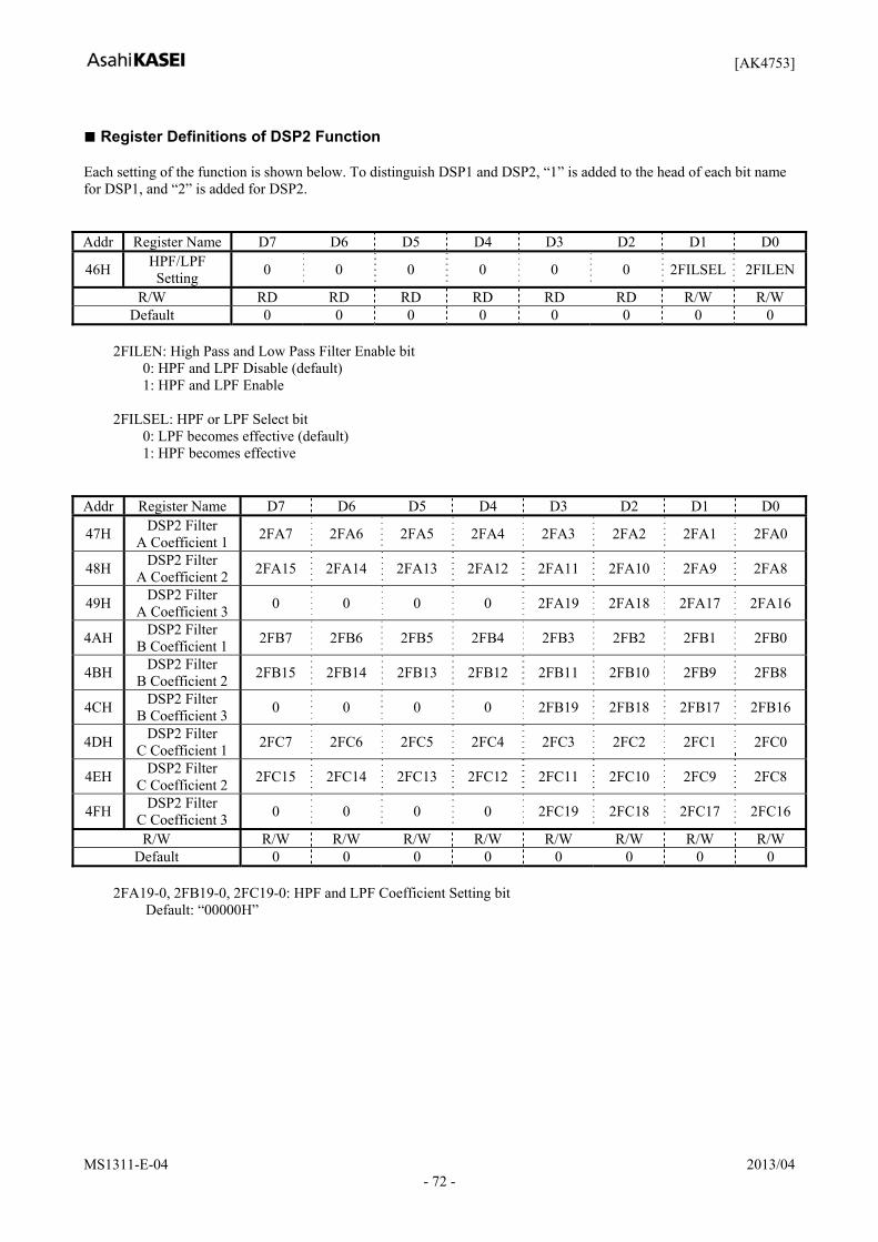
[AK4753]
MS1311-E-04 2013/04 - 72 -
Register Definitions of DSP2 Function Each setting of the function is shown below. To distinguish DSP1 and DSP2, “1” is added to the head of each bit name for DSP1, and “2” is added for DSP2. Addr Register Name D7 D6 D5 D4 D3 D2 D1 D0
46H HPF/LPF Setting 0 0 0 0 0 0 2FILSEL 2FILEN
R/W RD RD RD RD RD RD R/W R/W Default 0 0 0 0 0 0 0 0
2FILEN: High Pass and Low Pass Filter Enable bit
0: HPF and LPF Disable (default) 1: HPF and LPF Enable
2FILSEL: HPF or LPF Select bit
0: LPF becomes effective (default) 1: HPF becomes effective
Addr Register Name D7 D6 D5 D4 D3 D2 D1 D0
47H DSP2 Filter A Coefficient 1 2FA7 2FA6 2FA5 2FA4 2FA3 2FA2 2FA1 2FA0
48H DSP2 Filter A Coefficient 2 2FA15 2FA14 2FA13 2FA12 2FA11 2FA10 2FA9 2FA8
49H DSP2 Filter A Coefficient 3 0 0 0 0 2FA19 2FA18 2FA17 2FA16
4AH DSP2 Filter B Coefficient 1 2FB7 2FB6 2FB5 2FB4 2FB3 2FB2 2FB1 2FB0
4BH DSP2 Filter B Coefficient 2 2FB15 2FB14 2FB13 2FB12 2FB11 2FB10 2FB9 2FB8
4CH DSP2 Filter B Coefficient 3 0 0 0 0 2FB19 2FB18 2FB17 2FB16
4DH DSP2 Filter C Coefficient 1 2FC7 2FC6 2FC5 2FC4 2FC3 2FC2 2FC1 2FC0
4EH DSP2 Filter C Coefficient 2 2FC15 2FC14 2FC13 2FC12 2FC11 2FC10 2FC9 2FC8
4FH DSP2 Filter C Coefficient 3 0 0 0 0 2FC19 2FC18 2FC17 2FC16
R/W R/W R/W R/W R/W R/W R/W R/W R/W Default 0 0 0 0 0 0 0 0
2FA19-0, 2FB19-0, 2FC19-0: HPF and LPF Coefficient Setting bit
Default: “00000H”

[AK4753]
MS1311-E-04 2013/04 - 73 -
Addr Register Name D7 D6 D5 D4 D3 D2 D1 D0
50H DSP2 EQ Select 0 0 0 2EQ5 2EQ4 2EQ3 2EQ2 2EQ1
R/W RD RD RD R/W R/W R/W R/W R/W Default 0 0 0 0 0 0 0 0
2EQ1: Equalizer 1 Coefficient Setting Enable
0: Disable (default) 1: Enable
When 2EQ1 bit is “1”, settings of 2E1A19-0, 2E1B19-0 and 2E1C19-0 bits are enabled. When 2EQ1 bit is “0”, the audio data passes this block by 0dB gain.
2EQ2: Equalizer 2 Coefficient Setting Enable
0: Disable (default) 1: Enable
When 2EQ2 bit is “1”, settings of 2E2A19-0, 2E2B19-0 and 2E2C19-0 bits are enabled. When 2EQ2 bit is “0”, the audio data passes this block by 0dB gain.
2EQ3: Equalizer 3 Coefficient Setting Enable
0: Disable (default) 1: Enable
When 2EQ3 bit is “1”, settings of 2E3A19-0, 2E3B19-0 and 2E3C19-0 bits are enabled. When 2EQ3 bit is “0”, the audio data passes this block by 0dB gain.
2EQ4: Equalizer 4 Coefficient Setting Enable
0: Disable (default) 1: Enable
When 2EQ4 bit is “1”, settings of 2E4A19-0, 2E4B19-0 and 2E4C19-0 bits are enabled. When 2EQ4 bit is “0”, the audio data passes this block by 0dB gain.
2EQ5: Equalizer 5 Coefficient Setting Enable
0: Disable (default) 1: Enable
When 2EQ5 bit is “1”, settings of 2E5A19-0, 2E5B19-0 and 2E5C19-0 bits are enabled. When 2EQ5 bit is “0”, the audio data passes this block by 0dB gain.
Addr Register Name D7 D6 D5 D4 D3 D2 D1 D0
51H DSP2 EQ1 A Coefficient 1 2E1A7 2E1A6 2E1A5 2E1A4 2E1A3 2E1A2 2E1A1 2E1A0
52H DSP2 EQ1 A Coefficient 2 2E1A15 2E1A14 2E1A13 2E1A12 2E1A11 2E1A10 2E1A9 2E1A8
53H DSP2 EQ1 A Coefficient 3 0 0 0 0 2E1A19 2E1A18 2E1A17 2E1A16
54H DSP2 EQ1 B Coefficient 1 2E1B7 2E1B6 2E1B5 2E1B4 2E1B3 2E1B2 2E1B1 2E1B0
55H DSP2 EQ1 B Coefficient 2 2E1B15 2E1B14 2E1B13 2E1B12 2E1B11 2E1B10 2E1B9 2E1B8
56H DSP2 EQ1 B Coefficient 3 0 0 0 0 2E1B19 2E1B18 2E1B17 2E1B16
57H DSP2 EQ1 C Coefficient 1 2E1C7 2E1C6 2E1C5 2E1C4 2E1C3 2E1C2 2E1C1 2E1C0
58H DSP2 EQ1 C Coefficient 2 2E1C15 2E1C14 2E1C13 2E1C12 2E1C11 2E1C10 2E1C9 2E1C8
59H DSP2 EQ1 C Coefficient 3 0 0 0 0 2E1C19 2E1C18 2E1C17 2E1C16

[AK4753]
MS1311-E-04 2013/04 - 74 -
Addr Register Name D7 D6 D5 D4 D3 D2 D1 D0
5AH DSP2 EQ2 A Coefficient 1 2E2A7 2E2A6 2E2A5 2E2A4 2E2A3 2E2A2 2E2A1 2E2A0
5BH DSP2 EQ2 A Coefficient 2 2E2A15 2E2A14 2E2A13 2E2A12 2E2A11 2E2A10 2E2A9 2E2A8
5CH DSP2 EQ2 A Coefficient 3 0 0 0 0 2E2A19 2E2A18 2E2A17 2E2A16
5DH DSP2 EQ2 B Coefficient 1 2E2B7 2E2B6 2E2B5 2E2B4 2E2B3 2E2B2 2E2B1 2E2B0
5EH DSP2 EQ2 B Coefficient 2 2E2B15 2E2B14 2E2B13 2E2B12 2E2B11 2E2B10 2E2B9 2E2B8
5FH DSP2 EQ2 B Coefficient 3 0 0 0 0 2E2B19 2E2B18 2E2B17 2E2B16
60H DSP2 EQ2 C Coefficient 1 2E2C7 2E2C6 2E2C5 2E2C4 2E2C3 2E2C2 2E2C1 2E2C0
61H DSP2 EQ2 C Coefficient 2 2E2C15 2E2C14 2E2C13 2E2C12 2E2C11 2E2C10 2E2C9 2E2C8
62H DSP2 EQ2 C Coefficient 3 0 0 0 0 2E2C19 2E2C18 2E2C17 2E2C16
63H DSP2 EQ3 A Coefficient 1 2E3A7 2E3A6 2E3A5 2E3A4 2E3A3 2E3A2 2E3A1 2E3A0
64H DSP2 EQ3 A Coefficient 2 2E3A15 2E3A14 2E3A13 2E3A12 2E3A11 2E3A10 2E3A9 2E3A8
65H DSP2 EQ3 A Coefficient 3 0 0 0 0 2E3A19 2E3A18 2E3A17 2E3A16
66H DSP2 EQ3 B Coefficient 1 2E3B7 2E3B6 2E3B5 2E3B4 2E3B3 2E3B2 2E3B1 2E3B0
67H DSP2 EQ3 B Coefficient 2 2E3B15 2E3B14 2E3B13 2E3B12 2E3B11 2E3B10 2E3B9 2E3B8
68H DSP2 EQ3 B Coefficient 3 0 0 0 0 2E3B19 2E3B18 2E3B17 2E3B16
69H DSP2 EQ3 C Coefficient 1 2E3C7 2E3C6 2E3C5 2E3C4 2E3C3 2E3C2 2E3C1 2E3C0
6AH DSP2 EQ3 C Coefficient 2 2E3C15 2E3C14 2E3C13 2E3C12 2E3C11 2E3C10 2E3C9 2E3C8
6BH DSP2 EQ3 C Coefficient 3 0 0 0 0 2E3C19 2E3C18 2E3C17 2E3C16
6CH DSP2 EQ4 A Coefficient 1 2E4A7 2E4A6 2E4A5 2E4A4 2E4A3 2E4A2 2E4A1 2E4A0
6DH DSP2 EQ4 A Coefficient 2 2E4A15 2E4A14 2E4A13 2E4A12 2E4A11 2E4A10 2E4A9 2E4A8
6EH DSP2 EQ4 A Coefficient 3 0 0 0 0 2E4A19 2E4A18 2E4A17 2E4A16
6FH DSP2 EQ4 B Coefficient 1 2E4B7 2E4B6 2E4B5 2E4B4 2E4B3 2E4B2 2E4B1 2E4B0
70H DSP2 EQ4 B Coefficient 2 2E4B15 2E4B14 2E4B13 2E4B12 2E4B11 2E4B10 2E4B9 2E4B8
71H DSP2 EQ4 B Coefficient 3 0 0 0 0 2E4B19 2E4B18 2E4B17 2E4B16
72H DSP2 EQ4 C Coefficient 1 2E4C7 2E4C6 2E4C5 2E4C4 2E4C3 2E4C2 2E4C1 2E4C0
73H DSP2 EQ4 C Coefficient 2 2E4C15 2E4C14 2E4C13 2E4C12 2E4C11 2E4C10 2E4C9 2E4C8
74H DSP2 EQ4 C Coefficient 3 0 0 0 0 2E4C19 2E4C18 2E4C17 2E4C16
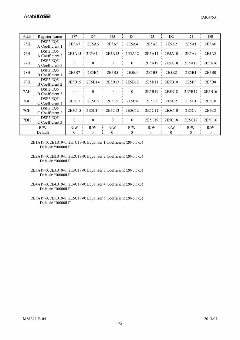
[AK4753]
MS1311-E-04 2013/04 - 75 -
Addr Register Name D7 D6 D5 D4 D3 D2 D1 D0
75H DSP2 EQ5 A Coefficient 1 2E5A7 2E5A6 2E5A5 2E5A4 2E5A3 2E5A2 2E5A1 2E5A0
76H DSP2 EQ5 A Coefficient 2 2E5A15 2E5A14 2E5A13 2E5A12 2E5A11 2E5A10 2E5A9 2E5A8
77H DSP2 EQ5 A Coefficient 3 0 0 0 0 2E5A19 2E5A18 2E5A17 2E5A16
78H DSP2 EQ5 B Coefficient 1 2E5B7 2E5B6 2E5B5 2E5B4 2E5B3 2E5B2 2E5B1 2E5B0
79H DSP2 EQ5 B Coefficient 2 2E5B15 2E5B14 2E5B13 2E5B12 2E5B11 2E5B10 2E5B9 2E5B8
7AH DSP2 EQ5 B Coefficient 3 0 0 0 0 2E5B19 2E5B18 2E5B17 2E5B16
7BH DSP2 EQ5 C Coefficient 1 2E5C7 2E5C6 2E5C5 2E5C4 2E5C3 2E5C2 2E5C1 2E5C0
7CH DSP2 EQ5 C Coefficient 2 2E5C15 2E5C14 2E5C13 2E5C12 2E5C11 2E5C10 2E5C9 2E5C8
7DH DSP2 EQ5 C Coefficient 3 0 0 0 0 2E5C19 2E5C18 2E5C17 2E5C16
R/W R/W R/W R/W R/W R/W R/W R/W R/W Default 0 0 0 0 0 0 0 0
2E1A19-0, 2E1B19-0, 2E1C19-0: Equalizer 1 Coefficient (20-bit x3)
Default: “00000H”
2E2A19-0, 2E2B19-0, 2E2C19-0: Equalizer 2 Coefficient (20-bit x3) Default: “00000H”
2E3A19-0, 2E3B19-0, 2E3C19-0: Equalizer 3 Coefficient (20-bit x3)
Default: “00000H”
2E4A19-0, 2E4B19-0, 2E4C19-0: Equalizer 4 Coefficient (20-bit x3) Default: “00000H”
2E5A19-0, 2E5B19-0, 2E5C19-0: Equalizer 5 Coefficient (20-bit x3)
Default: “00000H”
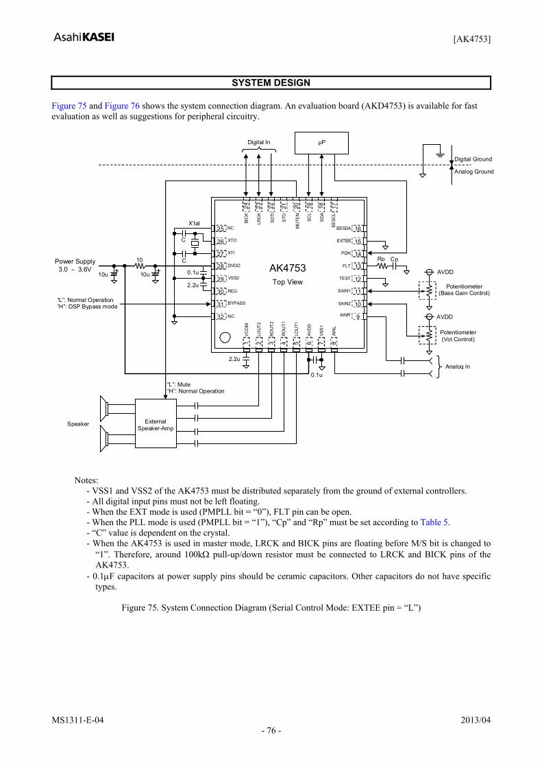
[AK4753]
MS1311-E-04 2013/04 - 76 -
SYSTEM DESIGN
Figure 75 and Figure 76 shows the system connection diagram. An evaluation board (AKD4753) is available for fast evaluation as well as suggestions for peripheral circuitry. μP
Power Supply 3.0 ∼ 3.6V
10u
Potentiometer(Vol Control)
NC
XTO
XTI
DVDD
VSS2
REG
BYPASS
NC
BIC
K
LRC
K
SD
TI
STO
MU
TEN
EESC
L
LOU
T2
RO
UT2
RO
UT1
LOU
T1
AVD
D
VSS
1
AIN
L
EESDA
EXTEE
PDN
FLT
TEST
SAIN1
SAIN2
AINR
AK4753Top View
25
26
27
28
29
30
31
32
24
23
16
15
14
13
12
11
10
9
22
21
20
19
18
1 2 3 4 5 6 7 8
SCL
SD
A
Speaker ExternalSpeaker-Amp
Analog Ground
Digital Ground
Cp 10 Rp
VC
OM
X’tal
C
C
Potentiometer (Bass Gain Control)
17
AVDD
2.2u
0.1u
AVDD
Analog In
0.1u
2.2u
10u
“L”: Mute “H”: Normal Operation
Digital In
“L”: Normal Operation “H”: DSP Bypass mode
Notes: - VSS1 and VSS2 of the AK4753 must be distributed separately from the ground of external controllers. - All digital input pins must not be left floating. - When the EXT mode is used (PMPLL bit = “0”), FLT pin can be open. - When the PLL mode is used (PMPLL bit = “1”), “Cp” and “Rp” must be set according to Table 5. - “C” value is dependent on the crystal. - When the AK4753 is used in master mode, LRCK and BICK pins are floating before M/S bit is changed to
“1”. Therefore, around 100kΩ pull-up/down resistor must be connected to LRCK and BICK pins of the AK4753.
- 0.1μF capacitors at power supply pins should be ceramic capacitors. Other capacitors do not have specific types.
Figure 75. System Connection Diagram (Serial Control Mode: EXTEE pin = “L”)
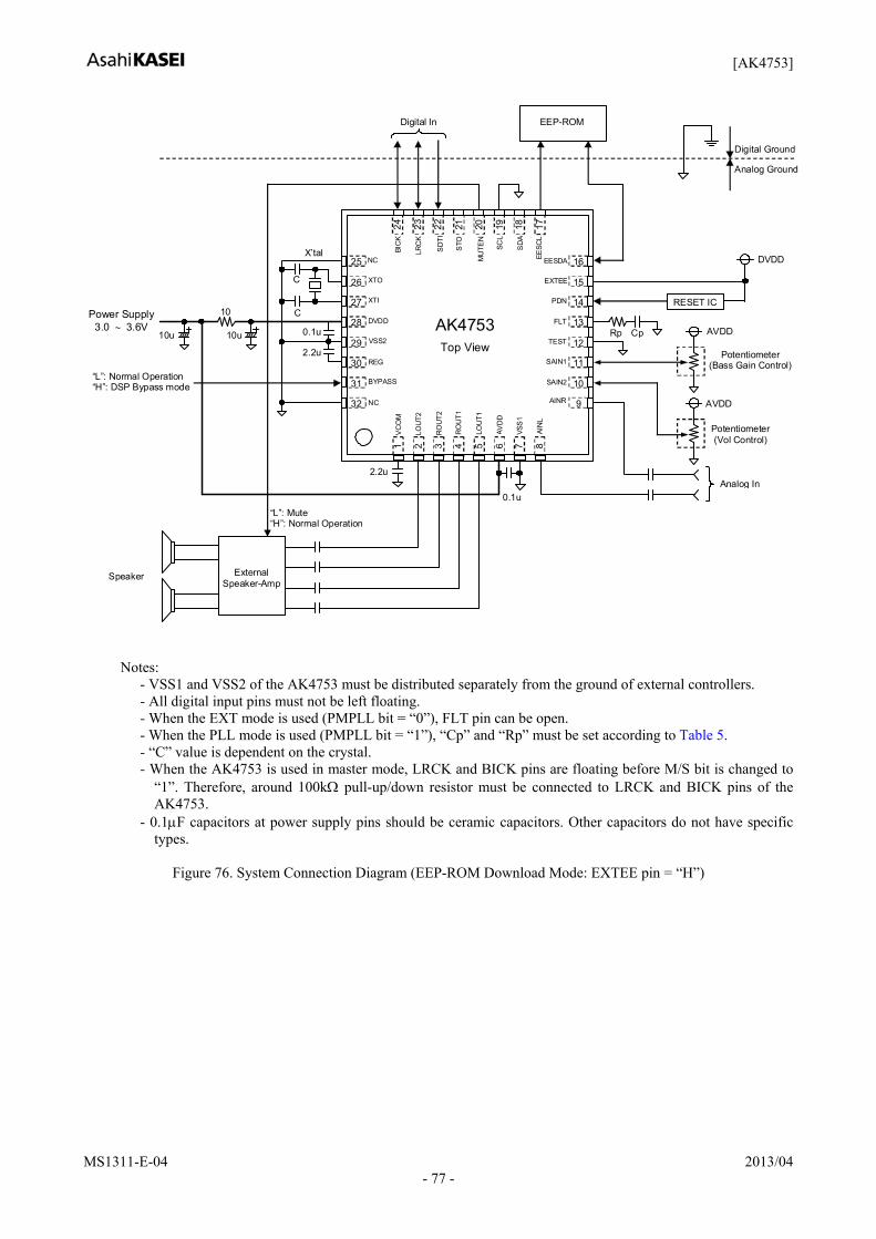
[AK4753]
MS1311-E-04 2013/04 - 77 -
EEP-ROM
Power Supply 3.0 ∼ 3.6V
10u
Potentiometer(Vol Control)
NC
XTO
XTI
DVDD
VSS2
REG
BYPASS
NC BI
CK
LRC
K
SD
TI
STO
MU
TEN
EESC
L
LOU
T2
RO
UT2
RO
UT1
LOU
T1
AVD
D
VSS
1
AIN
L
EESDA
EXTEE
PDN
FLT
TEST
SAIN1
SAIN2
AINR
AK4753Top View
25
26
27
28
29
30
31
32 24
23
16
15
14
13
12
11
10
9
22
21
20
19
18
1 2 3 4 5 6 7 8
SCL
SD
A
Speaker ExternalSpeaker-Amp
Analog Ground
Digital Ground
Cp
10
Rp
VC
OM
X’tal
C
C
Potentiometer (Bass Gain Control)
17
AVDD
2.2u
0.1u
AVDD
Analog In
0.1u
2.2u
10u
“L”: Mute “H”: Normal Operation
Digital In
DVDD
RESET IC
“L”: Normal Operation “H”: DSP Bypass mode
Notes: - VSS1 and VSS2 of the AK4753 must be distributed separately from the ground of external controllers. - All digital input pins must not be left floating. - When the EXT mode is used (PMPLL bit = “0”), FLT pin can be open. - When the PLL mode is used (PMPLL bit = “1”), “Cp” and “Rp” must be set according to Table 5. - “C” value is dependent on the crystal. - When the AK4753 is used in master mode, LRCK and BICK pins are floating before M/S bit is changed to
“1”. Therefore, around 100kΩ pull-up/down resistor must be connected to LRCK and BICK pins of the AK4753.
- 0.1μF capacitors at power supply pins should be ceramic capacitors. Other capacitors do not have specific types.
Figure 76. System Connection Diagram (EEP-ROM Download Mode: EXTEE pin = “H”)
[AK4753]
MS1311-E-04 2013/04 - 78 -
1. Grounding and Power Supply Decoupling The AK4753 requires careful attention to power supply and grounding arrangements. If AVDD and DVDD are supplied separately, the power-up sequence is not critical. VSS1 and VSS2 of the AK4753 must be connected to the analog ground plane. System analog ground and digital ground must be connected together near to where the supplies are brought onto the printed circuit board. Decoupling capacitors must be as near to the AK4753 as possible, with the small value ceramic capacitor being the nearest. 2. Internal Regulated Voltage Power Supply The input voltage to the REG pin is used as power supply (typ. 1.8V) for the internal digital circuit. A 2.2μF±50% ceramic capacitor connected between the REG and VSS2 pins eliminates the effects of high frequency noise. This capacitor in particular should be connected as close as possible to the pin. No load current may be drawn from the REG pin. All digital signals, especially clocks, should be kept away from the REG pin in order to avoid unwanted coupling into the AK4753. 3. Voltage Reference VCOM is a signal ground of this chip. A 2.2μF±50% ceramic capacitor connected between this pin and the VSS1 pin eliminates the effects of high frequency noise. This capacitor in particular should be connected as close as possible to the pin. No load current may be drawn from the VCOM pin. All digital signals, especially clocks, must be kept away from the VCOM pin in order to avoid unwanted coupling into the AK4753. 4. Analog Inputs The line inputs are single-ended. The input signal range scales with nominally at typ. 2.64Vpp (0.8 x AVDD), centered around the internal signal ground (AVDD/2). Usually the input signal is AC coupled using a capacitor. The cut-off frequency is fc = 1/ (2πRC). The AK4753 can accept input voltages from VSS1 to AVDD. 5. Analog Outputs The input data format for the DAC is 2’s complement. The output voltage is a positive full scale for 7FFFFFH (@24-bit) and a negative full scale for 800000H (@24-bit). The ideal output is VCOM voltage for 000000H (@24-bit). The line outputs are single-ended or differential and centered at AVDD/2.
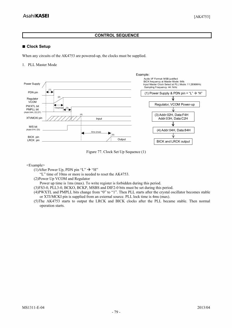
[AK4753]
MS1311-E-04 2013/04 - 79 -
CONTROL SEQUENCE
Clock Setup When any circuits of the AK4753 are powered-up, the clocks must be supplied. 1. PLL Master Mode
BICK pinLRCK pin
PWXTL bitPMPLL bit
(Addr:04H, D2,D7)
4ms (max)
Output
(1)
(5)
Power Supply
PDN pin
RegulatorVCOM
(2)
XTI/MCKI pin(4)
(3)
Input
M/S bit(Addr:01H, D3)
1ms(max)
Example: Audio I/F Format: MSB justified BICK frequency at Master Mode: 64fs Input Master Clock Select at PLL Mode: 11.2896MHz Sampling Frequency: 44.1kHz
(1) Power Supply & PDN pin = “L” “H”
(3) Addr:02H, Data:F4H Addr:03H, Data:C2H
Regulator, VCOM Power-up
(4) Addr:04H, Data:84H
BICK and LRCK output
Figure 77. Clock Set Up Sequence (1)
<Example>
(1) After Power Up, PDN pin “L” “H” “L” time of 10ms or more is needed to reset the AK4753.
(2) Power Up VCOM and Regulator Power up time is 1ms (max). To write register is forbidden during this period.
(3) FS3-0, PLL3-0, BCKO, BCKP, MSBS and DIF2-0 bits must be set during this period. (4) PWXTL and PMPLL bits change from “0” to “1”. Then PLL starts after the crystal oscillator becomes stable
or XTI/MCKI pin is supplied from an external source. PLL lock time is 4ms (max). (5) The AK4753 starts to output the LRCK and BICK clocks after the PLL became stable. Then normal
operation starts.
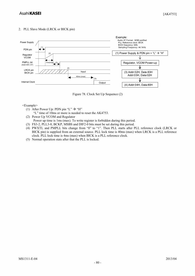
[AK4753]
MS1311-E-04 2013/04 - 80 -
2. PLL Slave Mode (LRCK or BICK pin)
Internal Clock
PMPLL bit(Addr:04H, D7)
40ms (max)
Output
(1)
(5)
Power Supply
PDN pin
RegulatorVCOM
(2)
LRCK pinBICK pin
(4)
(3)
Input
1ms(max)
4fs of
Example:Audio I/F Format : MSB justified PLL Reference clock: BICK BICK frequency: 64fs Sampling Frequency: 44.1kHz
(1) Power Supply & PDN pin = “L” “H”
(4) Addr:04H, Data:80H
(3) Addr:02H, Data:83H Addr:03H, Data:02H
Regulator, VCOM Power-up
Figure 78. Clock Set Up Sequence (2)
<Example>
(1) After Power Up: PDN pin “L” “H” “L” time of 10ms or more is needed to reset the AK4753.
(2) Power Up VCOM and Regulator Power up time is 1ms (max). To write register is forbidden during this period.
(3) FS3-2, PLL3-0, BCKP, MSBS and DIF2-0 bits must be set during this period. (4) PWXTL and PMPLL bits change from “0” to “1”. Then PLL starts after PLL reference clock (LRCK or
BICK pin) is supplied from an external source. PLL lock time is 40ms (max) when LRCK is a PLL reference clock. PLL lock time is 4ms (max) when BICK is a PLL reference clock.
(5) Normal operation stats after that the PLL is locked.
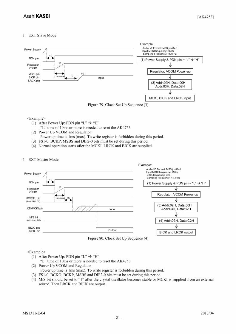
[AK4753]
MS1311-E-04 2013/04 - 81 -
3. EXT Slave Mode
(1)
Power Supply
PDN pin
RegulatorVCOM
(2)
MCKI pinBICK pinLRCK pin
(4)(3)
Input1ms(max)
Example:
(1) Power Supply & PDN pin = “L” “H”
MCKI, BICK and LRCK input
(3) Addr:02H, Data:00H Addr:03H, Data:02H
Regulator, VCOM Power-up
Audio I/F Format: MSB justified Input MCKI frequency: 256fs Sampling Frequency: 44.1kHz
Figure 79. Clock Set Up Sequence (3)
<Example> (1) After Power Up: PDN pin “L” “H”
“L” time of 10ms or more is needed to reset the AK4753. (2) Power Up VCOM and Regulator
Power up time is 1ms (max). To write register is forbidden during this period. (3) FS1-0, BCKP, MSBS and DIF2-0 bits must be set during this period. (4) Normal operation starts after the MCKI, LRCK and BICK are supplied.
4. EXT Master Mode
BICK pinLRCK pin
PWXTL bit(Addr:04H, D2)
Output
(1)
Power Supply
PDN pin
RegulatorVCOM
(2)
XTI/MCKI pin
(3)
Input
M/S bit(Addr:03H, D6)
1ms(max)
(4)
Example: Audio I/F Format: MSB justified Input MCKI frequency: 256fs BICK frequency: 64fs Sampling Frequency: 44.1kHz
(1) Power Supply & PDN pin = “L” “H”
(3) Addr:02H, Data:00H Addr:03H, Data:82H
Regulator, VCOM Power-up
(4) Addr:03H, Data:C2H
BICK and LRCK output Figure 80. Clock Set Up Sequence (4)
<Example> (1) After Power Up: PDN pin “L” “H”
“L” time of 10ms or more is needed to reset the AK4753. (2) Power Up VCOM and Regulator
Power up time is 1ms (max). To write register is forbidden during this period. (3) FS1-0, BCKO, BCKP, MSBS and DIF2-0 bits must be set during this period. (4) M/S bit should be set to “1” after the crystal oscillator becomes stable or MCKI is supplied from an external
source. Then LRCK and BICK are output.
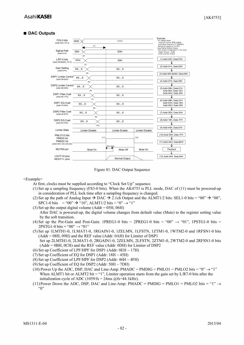
[AK4753]
MS1311-E-04 2013/04 - 82 -
DAC Outputs FS3-0 bits
(Addr:02H, D7-4)0000
Normal Output
(1)
(9)
(7)
(11) (12)
Siglnal Path(Addr:01H)
00HFFH(3)
(8)
(2)
(6)
DSP1 Limiter Control(Addr:08-0AH)
XX....X(4)
DSP2 Limiter Control(Addr:0B-0DH)
(5)
DSP1 EQ Coef(Addr:18-45H)
00H E0H
L/R7-0 bits(Addr:05H&06H, D7-0)
DSP1 Filter Coef(Addr:0E-17H)
DSP2 EQ Coef(Addr:50-7DH)
DSP2 Filter Coef(Addr:46-4FH)
PMLO1/2 bitsPMDIG bitPMADC bit
(Addr:04H, D5-4,D3,D0)
(10)
Gain Setting(Addr:07H)
Limiter State Limiter Disable Limiter Enable Limiter Disable
LOUT1/2 pinsMOUT+/- pins
MUTEN pin Mute OffMute On4ms (typ)
1111
XX....X
XX....X
XX....X
XX....X
XX....X
XX....X
XX....X
XX....X
XX....X
XX....X
XX....X
XX....X
XX....X
Mute On
Example:PLL Master Mode Audio I/F Format: MSB justified Input MCKI frequency:11.2896MHz Sampling Frequency: 44.1kHz Input Signal Setting: Analog DAC Output Configuration: 2.1ch mode Digital Volume: −30dB Limiter and EQ: Enable
(2) Addr:01H, Data:E0H
(1) Addr:02H, Data:F4H
(9) Addr:46H, Data:01H
(10) Addr:50H, Data:1FH
(11) Addr:04H, Data:BDH
(12) Addr:04H, Data:84H
Playback
(3) Addr:05H &06H, Data:00H
(7) Addr:0EH, Data:03H
(5) Addr:08H, Data:01H Addr:09H, Data:1EH Addr:0AH, Data:30H
(6) Addr:0BH, Data:01H Addr:0CH, Data:1EH Addr:0DH, Data:30H
(4) Addr:07H, Data:55H
(8) Addr:18H, Data:1FH
Figure 81. DAC Output Sequence <Example>
At first, clocks must be supplied according to “Clock Set Up” sequence. (1) Set up a sampling frequency (FS3-0 bits). When the AK4753 is PLL mode, DAC of (11) must be powered-up
in consideration of PLL lock time after a sampling frequency is changed. (2) Set up the path of Analog Input DAC 2.1ch Output and the ALMT1/2 bits: SEL1-0 bits = “00” “00”,
SPC1-0 bits = “00” “10”, ALMT1/2 bits = “0” → “1” (3) Set up the output digital volume (Addr = 05H, 06H)
After DAC is powered-up, the digital volume changes from default value (Mute) to the register setting value by the soft transition.
(4) Set up the Pre-Gain and Post-Gain: 1PREG1-0 bits = 2PREG1-0 bits = “00” → “01”, 1PSTG1-0 bits = 2PSTG1-0 bits = “00” → “01”
(5) Set up 1LMTH1-0, 1LMAT1-0, 1RGAIN1-0, 1ZELMN, 1LFSTN, 1ZTM1-0, 1WTM2-0 and 1RFSN1-0 bits (Addr = 08H, 09H) and the REF value (Addr: 0AH) for Limiter of DSP1 Set up 2LMTH1-0, 2LMAT1-0, 2RGAIN1-0, 2ZELMN, 2LFSTN, 2ZTM1-0, 2WTM2-0 and 2RFSN1-0 bits (Addr = 0BH, 0CH) and the REF value (Addr: 0DH) for Limiter of DSP2
(6) Set up Coefficient of LPF/HPF for DSP1 (Addr: 0EH ~ 17H) (7) Set up Coefficient of EQ for DSP1 (Addr: 18H ~ 45H) (8) Set up Coefficient of LPF/HPF for DSP2 (Addr: 46H ~ 4FH) (9) Set up Coefficient of EQ for DSP2 (Addr: 50H ~ 7DH) (10) Power Up the ADC, DSP, DAC and Line-Amp: PMADC = PMDIG = PMLO1 = PMLO2 bits = “0” → “1”
When ALMT1 bit or ALMT2 bit = “1”, Limiter operation starts from the gain set by L/R7-0 bits after the initialization cycle of ADC (1059/fs = 24ms @fs=44.1kHz).
(11) Power Down the ADC, DSP, DAC and Line-Amp: PMADC = PMDIG = PMLO1 = PMLO2 bits = “1” → “0”
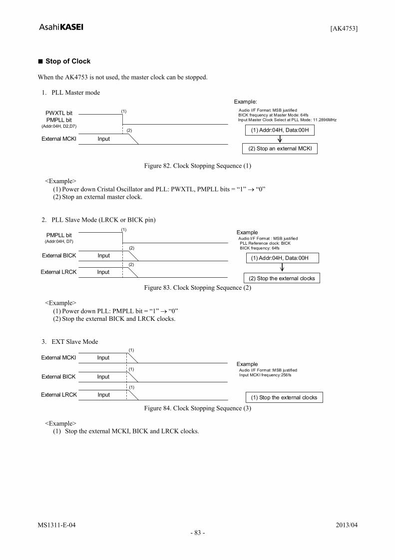
[AK4753]
MS1311-E-04 2013/04 - 83 -
Stop of Clock When the AK4753 is not used, the master clock can be stopped.
1. PLL Master mode
External MCKI
PWXTL bitPMPLL bit
(Addr:04H, D2,D7)
Input(2)
(1)
Example: Audio I/F Format: MSB justified BICK frequency at Master Mode: 64fs Input Master Clock Select at PLL Mode: 11.2896MHz
(2) Stop an external MCKI
(1) Addr:04H, Data:00H
Figure 82. Clock Stopping Sequence (1)
<Example> (1) Power down Cristal Oscillator and PLL: PWXTL, PMPLL bits = “1” → “0” (2) Stop an external master clock.
2. PLL Slave Mode (LRCK or BICK pin)
External BICK
PMPLL bit(Addr:04H, D7)
Input
(1)
(2)
External LRCK Input(2)
ExampleAudio I/F Format : MSB justified PLL Reference clock: BICK BICK frequency: 64fs
(1) Addr:04H, Data:00H
(2) Stop the external clocks Figure 83. Clock Stopping Sequence (2)
<Example>
(1) Power down PLL: PMPLL bit = “1” → “0” (2) Stop the external BICK and LRCK clocks.
3. EXT Slave Mode
External LRCK Input(1)
External BICK Input(1)
External MCKI Input(1)
ExampleAudio I/F Format :MSB justified Input MCKI frequency:256fs
(1) Stop the external clocks
Figure 84. Clock Stopping Sequence (3)
<Example> (1) Stop the external MCKI, BICK and LRCK clocks.

[AK4753]
MS1311-E-04 2013/04 - 84 -
4. EXT Master Mode
LRCK Output
BICK Output
External MCKI Input
(1)
"H" or "L"
"H" or "L"
PWXTL bit(Addr:04H, D2)
ExampleAudio I/F Format :MSB justified Input MCKI frequency:256fs
(1) Addr:04H, Data:00H or Stop the external MCKI
Figure 85. Clock Stopping Sequence (4)
<Example>
(1) Power down Cristal oscillator (PWXTL bit = “1” → “0”) or stop MCKI clock. BICK and LRCK are fixed to “H” or “L”.
Power Down Power supply current can also be shut down (typ. 1μA) by stopping clocks and setting PDN pin = “L”. When the PDN pin = “L”, the registers are initialized.
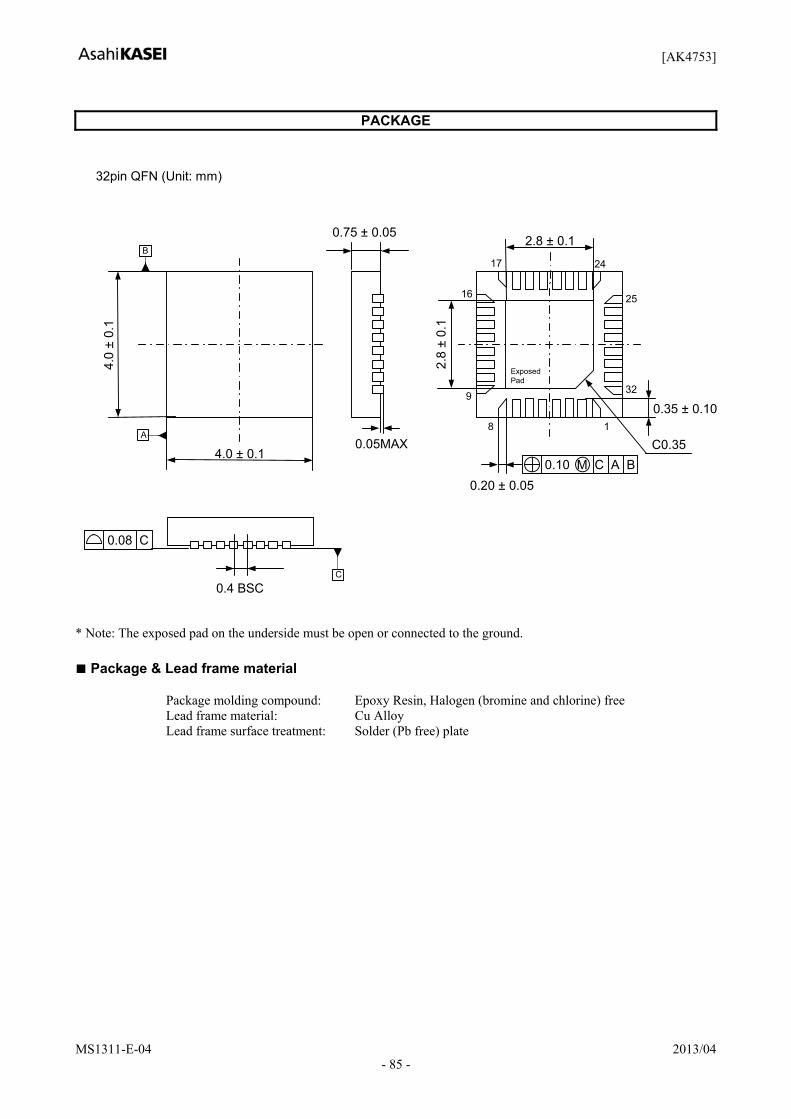
[AK4753]
MS1311-E-04 2013/04 - 85 -
PACKAGE
32pin QFN (Unit: mm)
2.8 ± 0.1
0.4 BSC
0.20 ± 0.05
2.8
± 0.
11
9
16 25
4.0 ± 0.1
4.0
± 0.
1
0.35 ± 0.10
B
A8
32
17 24
ExposedPad
C0.350.05MAX
0.75 ± 0.05
0.10 M C A B
0.08 C
C
* Note: The exposed pad on the underside must be open or connected to the ground. Package & Lead frame material
Package molding compound: Epoxy Resin, Halogen (bromine and chlorine) free Lead frame material: Cu Alloy Lead frame surface treatment: Solder (Pb free) plate
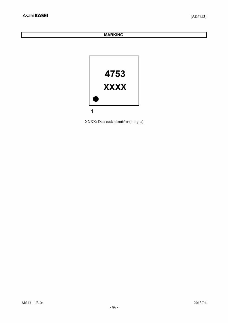
[AK4753]
MS1311-E-04 2013/04 - 86 -
MARKING
4753 XXXX
1
XXXX: Date code identifier (4 digits)

[AK4753]
MS1311-E-04 2013/04 - 87 -
REVISION HISTORY
Date (Y/M/D) Revision Reason Page Contents 11/07/15 00 First Edition 12/10/31 01 Specification
Change 11 Switching Characteristics
External Slave Mode BICK Input Timing, Period:
312.5ns → 312.5ns or 1/(126fs)s Note 16 was added.
13/02/06 02 Description Addition
21-23 PLL Mode A detailed description was added:
Note 23 and Note 24 were added. Table 6 was added.
13/03/21 03 Error Correction
21-23 PLL Mode Description and Note 23: MCKI pin → XTI/MCKI pin Table 6 was changed.
13/04/04 04 Error Correction
23 PLL Mode 3. Sampling Frequency setting in PLL Mode
PLL reference clock pin: BICK pin → LRCK or BICK pin

[AK4753]
MS1311-E-04 2013/04 - 88 -
IMPORTANT NOTICE
0. Asahi Kasei Microdevices Corporation (“AKM”) reserves the right to make changes to the
information contained in this document without notice. When you consider any use or application of AKM product stipulated in this document (“Product”), please make inquiries the sales office of AKM or authorized distributors as to current status of the Products.
1. All information included in this document are provided only to illustrate the operation and application examples of AKM Products. AKM neither makes warranties or representations with respect to the accuracy or completeness of the information contained in this document nor grants any license to any intellectual property rights or any other rights of AKM or any third party with respect to the information in this document. You are fully responsible for use of such information contained in this document in your product design or applications. AKM ASSUMES NO LIABILITY FOR ANY LOSSES INCURRED BY YOU OR THIRD PARTIES ARISING FROM THE USE OF SUCH INFORMATION IN YOUR PRODUCT DESIGN OR APPLICATIONS.
2. The Product is neither intended nor warranted for use in equipment or systems that require extraordinarily high levels of quality and/or reliability and/or a malfunction or failure of which may cause loss of human life, bodily injury, serious property damage or serious public impact, including but not limited to, equipment used in nuclear facilities, equipment used in the aerospace industry, medical equipment, equipment used for automobiles, trains, ships and other transportation, traffic signaling equipment, equipment used to control combustions or explosions, safety devices, elevators and escalators, devices related to electric power, and equipment used in finance-related fields. Do not use Product for the above use unless specifically agreed by AKM in writing.
3. Though AKM works continually to improve the Product’s quality and reliability, you are responsible for complying with safety standards and for providing adequate designs and safeguards for your hardware, software and systems which minimize risk and avoid situations in which a malfunction or failure of the Product could cause loss of human life, bodily injury or damage to property, including data loss or corruption.
4. Do not use or otherwise make available the Product or related technology or any information contained in this document for any military purposes, including without limitation, for the design, development, use, stockpiling or manufacturing of nuclear, chemical, or biological weapons or missile technology products (mass destruction weapons). When exporting the Products or related technology or any information contained in this document, you should comply with the applicable export control laws and regulations and follow the procedures required by such laws and regulations. The Products and related technology may not be used for or incorporated into any products or systems whose manufacture, use, or sale is prohibited under any applicable domestic or foreign laws or regulations.
5. Please contact AKM sales representative for details as to environmental matters such as the RoHS compatibility of the Product. Please use the Product in compliance with all applicable laws and regulations that regulate the inclusion or use of controlled substances, including without limitation, the EU RoHS Directive. AKM assumes no liability for damages or losses occurring as a result of noncompliance with applicable laws and regulations.
6. Resale of the Product with provisions different from the statement and/or technical features set forth in this document shall immediately void any warranty granted by AKM for the Product and shall not create or extend in any manner whatsoever, any liability of AKM.
7. This document may not be reproduced or duplicated, in any form, in whole or in part, without prior written consent of AKM.
Related Documents