Supplementary Information Low-Temperature Solution-Processed Li-Doped SnO 2 as an Effective Electron Transporting Layer for High-Performance Flexible and Wearable Perovskite Solar Cells Minwoo Park 1,2 , Jae-Yup Kim 1 , Hae Jung Son 1 , Chul-Ho Lee 3 , Seung Soon Jang 4 , and Min Jae Ko 1,3 1 Photo-Electronic Hybrids Research Center, Korea Institute of Science and Technology (KIST), Seoul 02792, Korea 2 Department of Chemical and Biological Engineering, Sookmyung Women’s University, Seoul 04310, Korea 3 KU-KIST Graduate School of Converging Science and Technology, Korea University, Seoul 02841, Korea 4 Computational NanoBio Technology Laboratory, School of Materials Science and Engineering, Georgia Institute of Technology, 771 Ferst Drive NW, Atlanta, Georgia 30332‐0245, USA 1

Welcome message from author
This document is posted to help you gain knowledge. Please leave a comment to let me know what you think about it! Share it to your friends and learn new things together.
Transcript

Supplementary Information
Low-Temperature Solution-Processed Li-Doped SnO2 as an
Effective Electron Transporting Layer for High-Performance
Flexible and Wearable Perovskite Solar Cells
Minwoo Park1,2
, Jae-Yup Kim1, Hae Jung Son1, Chul-Ho Lee3, Seung Soon Jang4, and Min Jae
Ko1,3
1Photo-Electronic Hybrids Research Center, Korea Institute of Science and Technology (KIST),
Seoul 02792, Korea2Department of Chemical and Biological Engineering, Sookmyung Women’s University, Seoul
04310, Korea3KU-KIST Graduate School of Converging Science and Technology, Korea University, Seoul
02841, Korea4Computational NanoBio Technology Laboratory, School of Materials Science and
Engineering, Georgia Institute of Technology, 771 Ferst Drive NW, Atlanta, Georgia 30332‐0245, USA
1

Figure S1. (A) X-ray diffraction (XRD) of CH3NH3PbI3 thin film. Inset shows the photograph of
the as-coated perovskite on FTO/Li:SnO2. (B) SEM image of perovskite.
Figure S2. Steady-state current density of SnO2- and Li:SnO2-device at the maximum power
voltages (Vmax), Vmax = 0.789 V and 0.848 V for SnO2- and Li:SnO2-device, respectively.
2

Figure S3. J-V curves and parameters of Li:SnO2-device for different annealing times (1 h and 2
h).
3

Figure S4. XPS spectra of Li:SnO2 thin film. Sn-3d, O-1s, and Cl-2p spectra and atomic
percentage correspond to (A), (B), and (C), respectively.
4
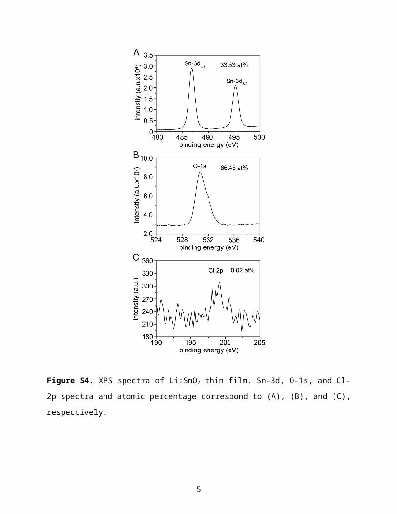
Figure S5. (A) Transmittance graph of FTO/SnO2 and FTO/Li:SnO2. (B) Tauc plots of SnO2 and
Li:SnO2. From the equation of αhν = B(hν-Eg)n ,where α is the absorption coefficient, B is the
proportionality constant, hν is the photon energy, and n is the constant (n = 0.5 for direct band
gap), band gap (Eg) was estimated to be 3.95 eV.
5

Figure S6. AFM images of bare FTO (A), FTO/SnO2 (B), and FTO/Li:SnO2 (C).
6
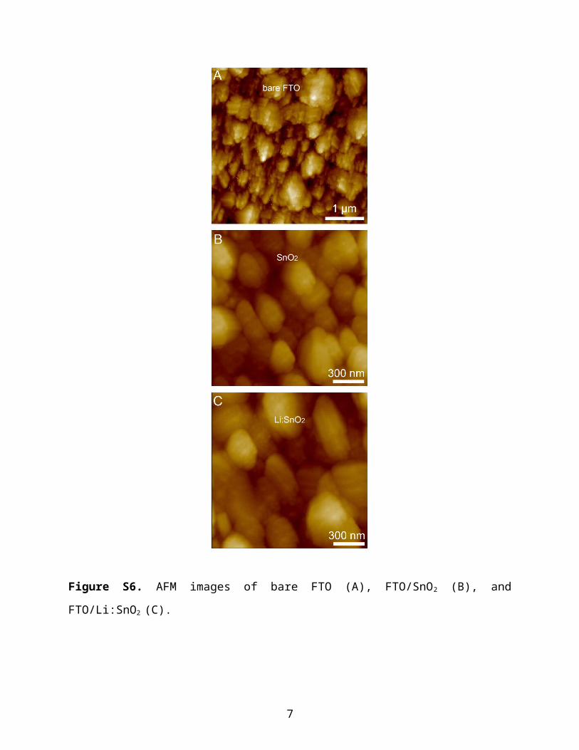
Figure S7. (A, B) AFM image and height profile of SnO2 on ITO/glass. (C, D) AFM image and
height profile of Li:SnO2 on ITO/glass.
Rs [Ω] Rtr [kΩ] Rrec [kΩ] Ctr [μF] Crec [μF]
SnO2 0.93 8.3 3.0 0.0128 0.0343Li:SnO2 0.91 6.5 6.8 0.0311 0.0192
Table S1. EIS parameters of the perovskite solar cells.
7

Figure S8. (A) Schematic of device architecture of flexible and wearable perovskite solar cell.
(B) J-V curve and parameters of the device.
8
Related Documents