Institute of Microelectronic Systems 19. Testing and Design for Testability 19: Testing 2 Institute of Microelectronic Systems Motivation • Stable chip manufacturing costs • Increasing testing costs: – Increasing number of gates/device – Limited number of pins – Increasing number of internal states – Increasing logical and sequential depth • Example: – Testing of a combinational circuit with n inputs (10 MHz, one test per cycle) • Testability has to be considered in all phases of design years 3656 60 years 3,5 50 day 1 40 s 107 30 s 3 25 time for test n

Welcome message from author
This document is posted to help you gain knowledge. Please leave a comment to let me know what you think about it! Share it to your friends and learn new things together.
Transcript

Institute of MicroelectronicSystems
19. Testing andDesign for Testability
19: Testing 2
Institute of MicroelectronicSystems
Motivation
• Stable chip manufacturing costs
• Increasing testing costs:– Increasing number of gates/device
– Limited number of pins
– Increasing number of internal states
– Increasing logical and sequential depth
• Example:– Testing of a combinational
circuit with n inputs
(10 MHz, one test per cycle)
• Testability has to be considered in all
phases of design
years365660
years3,550
day140
s10730
s325
time for testn

19: Testing 3
Institute of MicroelectronicSystems
Economical Considerations (1)
• Average Quality Level (AQL):
rtsAcceptedPa
artsDevectivePaql
#
#=
19: Testing 4
Institute of MicroelectronicSystems
Economical Considerations (2)
• Correlation: Fault Coverage and Defective Parts

19: Testing 5
Institute of MicroelectronicSystems
Economical Considerations (3)
• Correlation: Fault Coverage and Defective Parts
– DL(=AQL): Defect Level; Number of defective circuits which have been classified as correct working (testing with T )
– Y: yield
– T: fault coverage
TYDL −−= 11
19: Testing 6
Institute of MicroelectronicSystems
Economical Considerations (3)
Defect level as function of yield and fault coverage

19: Testing 7
Institute of MicroelectronicSystems
Design Flow: Testing (1)
19: Testing 8
Institute of MicroelectronicSystems
Design Flow: Testing (2)
• Chip Test after Manufacturing:
Manufacturing Process
Parametric Test (current/power dissipation)(erroneous chips are marked with color points and removed after sawing)
Chip Test on Tester

19: Testing 9
Institute of MicroelectronicSystems
Fundamental Definitions
• Relationship between faults, errors and failures:
• Fault: physical defect, imperfection or flaw which occurs in a hardware or software component
• Error: manifestation of a fault (erroneous information on a hardware line or in a program, caused by a fault)
• Failure: malfunction of a system
• Three-universe model of a system:
fault error failure
Physical Universe
Informational Universe
External Universe
Faults Errors Failures
19: Testing 10
Institute of MicroelectronicSystems
Fault Models (1)
• Basis: physical phenomena– Oxide defects
– Missing implants
– Lithographic defects
– Junction defects
– Metal shorts & opens
– Moisture accumulation
– Impurities / Contaminations
– Static discharge
• Examples for physical faults:

19: Testing 11
Institute of MicroelectronicSystems
Fault Models (2)
19: Testing 12
Institute of MicroelectronicSystems
Fault Models for Gates (1)
• The GATE model: Stuck-at– stuck @0
– stuck @1
– 1 fault at a time (single-stuck)
PHYSICAL (analog)
LOGICAL (digital)

19: Testing 13
Institute of MicroelectronicSystems
Fault Models for Gates (2)
• Issue: complexity– as 1 model .......................
• 12 faults
– as 12 gates ......................................................
• 30 (collapsed) faults
• 12x larger netlist
• 30x computation
– as 60 transistors ................
• 90 (collapsed) faults
• 60 transistors
• 400x computation
19: Testing 14
Institute of MicroelectronicSystems
Fault Models for Gates (3)
• The controversy:– IBM: comprehensive stuck-at no empirical need for MOS fault
models
– UNISYS: MOS model required for < 1% AQL

19: Testing 15
Institute of MicroelectronicSystems
Fault Models for Gates (4)
• The MOS problem: Gates Memory
• Example: the output floats ..................................– Fault-free: C always driven
– Fault: C un-driven;
assumes last value;
sequential !
• Need 2-pattern test ...........– set C to opposite
– test0111c
1011b
1101
1110
1100a
BABAbranch
TestSet
Anything works !
19: Testing 16
Institute of MicroelectronicSystems
Fault Tolerant Design (1)
• Fault tolerance achieved by redundancy techniques:– Duplication with Complementary Logic
– Self-Checking Logic
– Reconfigurable Array Structures
Fault detection by duplication with complementary logic

19: Testing 17
Institute of MicroelectronicSystems
Fault Tolerant Design (2)
4-by-4 array with one spare column
19: Testing 18
Institute of MicroelectronicSystems
Fault Tolerant Design (3)
Reconfigured array

19: Testing 19
Institute of MicroelectronicSystems
Test Pattern Generation (1)
• manually
• pseudo random (leads up to 60% fault coverage)
• algorithmic
• special test patterns for RAMs
• fault coverage sufficient ?fault simulation
19: Testing 20
Institute of MicroelectronicSystems
The D-Algorithm (1)
• Every test generation procedure has to solve the following problems:– Creation of a change at the faulty line– Propagation of the change to the primary output line
• In the D-Algorithm the symbols and are used to refer to the changes. and are used as follows:
– : used if a line has the value 1 in absence of a fault and the value 0 in case of a fault occurrence
– :used if a line has the value 0 if no fault occurs and otherwise the value 1
• The D-algorithm method for path sensitization consists of two principal phases:
– forward drive (propagation) of an D-value to an primary output – backward trace (consistency operation)
• These two steps are iterated for different propagation paths for the D-value from one dedicated internal point i to one dedicated primary output point o until the backward trace phase is finished without any contradiction (a test vector for a fault at i has been found) or until all possible paths from i to o have been examined.
DDDD
D
D
19: Testing 21
Institute of MicroelectronicSystems
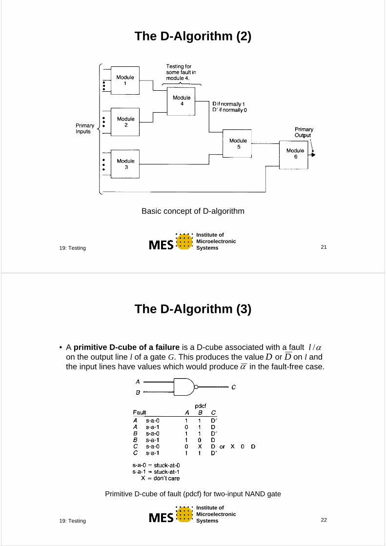
The D-Algorithm (2)
Basic concept of D-algorithm
19: Testing 22
Institute of MicroelectronicSystems
The D-Algorithm (3)
• A primitive D-cube of a failure is a D-cube associated with a fault on the output line l of a gate G. This produces the value or on l and the input lines have values which would produce in the fault-free case.
Primitive D-cube of fault (pdcf) for two-input NAND gate
α/lDD
α

19: Testing 23
Institute of MicroelectronicSystems
The D-Algorithm (4)
• A propagation D-cube of a failure specifies the propagation of changes at one (or more) inputs of a gate G to its inputs l.
Propagation D-cube (pdc) for two-input NAND gate
19: Testing 24
Institute of MicroelectronicSystems
The D-Algorithm (5)
• A singular cover of a gate G is a {0, 1, X} truth table representationof G.
Singular cover for two-input NAND gate

19: Testing 25
Institute of MicroelectronicSystems
The D-Algorithm (6)
Singular covers for several basic logic gates
19: Testing 26
Institute of MicroelectronicSystems
The D-Algorithm (7)
Construction of the singular cover of a logic module
19: Testing 27
Institute of MicroelectronicSystems
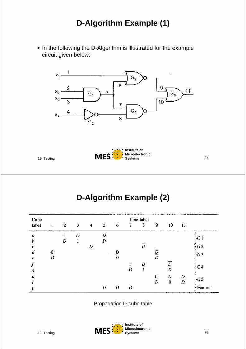
D-Algorithm Example (1)
• In the following the D-Algorithm is illustrated for the example circuit given below:
19: Testing 28
Institute of MicroelectronicSystems
D-Algorithm Example (2)
Propagation D-cube table

19: Testing 29
Institute of MicroelectronicSystems
D-Algorithm Example (3)
Singular cover table
19: Testing 30
Institute of MicroelectronicSystems
D-Algorithm Example (4)
D-cube intersection table

19: Testing 31
Institute of MicroelectronicSystems
D-Algorithm Example (5)
• Running the D-Algorithm for generating a test for line 5/0:1) Start with D-cube for the fault 5/0:
2) The D of line 5 is automatically propagated to line 6 and 7 by cube j
3) Now the propagation along path 6 9 11 is considered: D on line 6 is propagated to line 9 by cube d. Combining d and k yields cube l:
19: Testing 32
Institute of MicroelectronicSystems
D-Algorithm Example (6)
• Running the D-Algorithm (continued):4) If cube i is used with instead of D, the propagation to the output
can be done:
5) Now the consistency phase is started and a value for line 4 has to be found. From the singular cover table it can be seen that a 0 on line 10 implies both line 7 and line 8 to be 1. In cube m line 7 is a D(and also line 5 which is connected to 7 by j), and this D must now be set to 1 which is a contradiction that disables the path sensitization 5 6/7 9 11.
D
19: Testing 33
Institute of MicroelectronicSystems
D-Algorithm Example (7)
• Running the D-Algorithm (continued):6) Starting the propagation along 5 7 10 11 leads to the
following cube:
7) From the singular cover table we get the information that a 1 on line 8 is the same as a 0 on line 4. Additionally, it can be seen that the 0 on line 9 can be obtained by a 1 on line 1.
8) This yields the final cube:
1 1 1 0 D D D 1 0
9) A test vector for line 5/0 is given by:
1 1 1 0
D D
19: Testing 34
Institute of MicroelectronicSystems
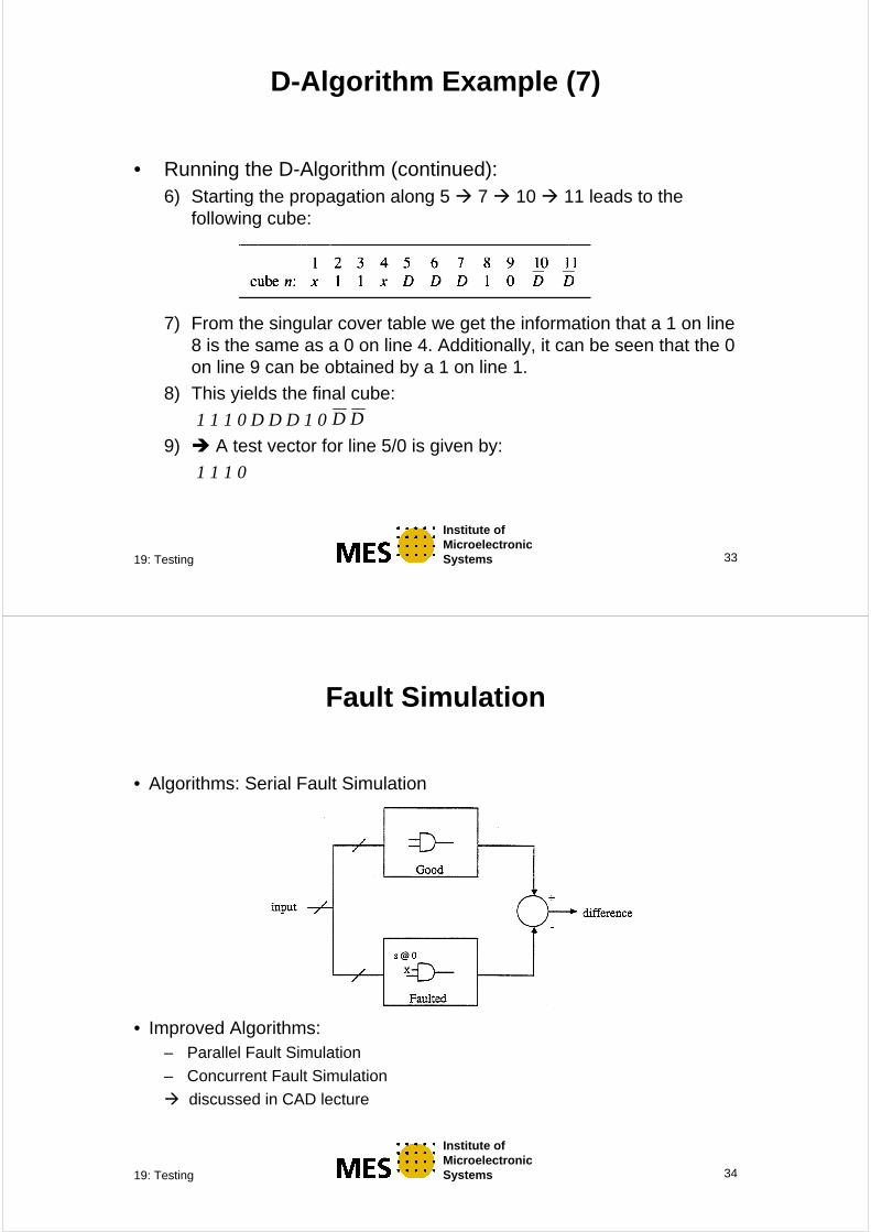
Fault Simulation
• Algorithms: Serial Fault Simulation
• Improved Algorithms:– Parallel Fault Simulation
– Concurrent Fault Simulation
discussed in CAD lecture

19: Testing 35
Institute of MicroelectronicSystems
Design for Testability (1)
• Circuit level: restriction of physically possible faults
• Logic level: restrict possibilities of realizations
• System level: restrict size of component and number of states
Testability:
• controllability
• observability
• additional chip area required
• shorter design cycle
Methods to improve controllability and observability:
• ad-hoc techniques
• structured approaches
19: Testing 36
Institute of MicroelectronicSystems
Design for Testability (2)
Design for testability: complex gate (a) not testable with stuck-at model; (b) fully testable with stuck-at model
19: Testing 37
Institute of MicroelectronicSystems
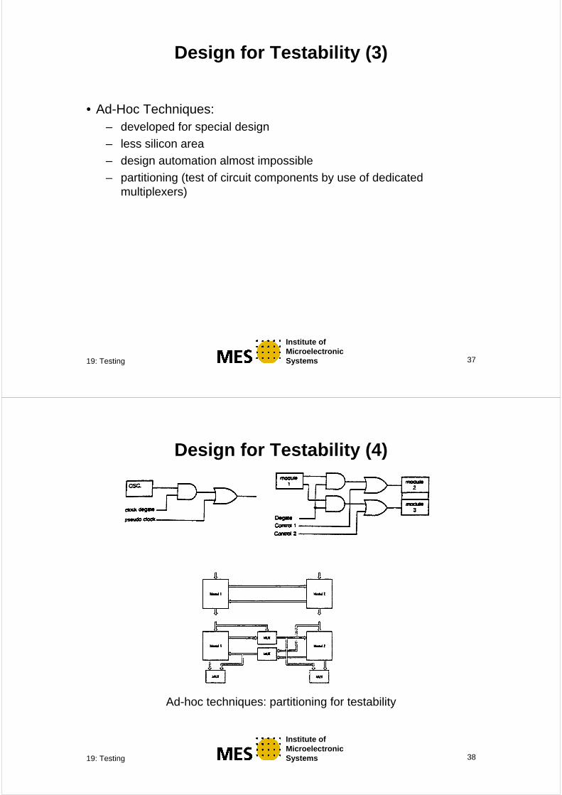
Design for Testability (3)
• Ad-Hoc Techniques:– developed for special design
– less silicon area
– design automation almost impossible
– partitioning (test of circuit components by use of dedicated multiplexers)
19: Testing 38
Institute of MicroelectronicSystems
Design for Testability (4)
Ad-hoc techniques: partitioning for testability

19: Testing 39
Institute of MicroelectronicSystems
Design for Testability (5)
A-hoc techniques: insertion of register in order to limit logic depth to a given maximum value
19: Testing 40
Institute of MicroelectronicSystems
Design for Testability (6)
Ad-hoc techniques :test shift registers for PLA test (increasing PLA area)

19: Testing 41
Institute of MicroelectronicSystems
Scan-Path Methods (1)
• Main idea: test of sequential network is reduced to test of combinational network
• for circuits consisting of logic with some feedbacks
• can be realized by reconfiguration of latches as shift registers (two modes of use)
Feedback logic with scan-path
19: Testing 42
Institute of MicroelectronicSystems
Scan-Path Methods (2)
• Test scan-path / register function first:– Flush test ( 0...010...0 ) or
– Shift test ( 00110011... ) (each register transfer is tested by this combination: 0 0, 0 1, 1 1, 1 0 ).
• Cycle for testing combinational logic function:1) Scan mode: Preload Y and set PI
2) System operation mode: Wait until inputs of Y are steady. Clock new state into Y.
3) Shift state out. Compare PO and state values with expected responses.

19: Testing 43
Institute of MicroelectronicSystems
Scan-Path Methods (3)
• Advantages:– Testability of clocked circuits is improved and guaranteed at design
stage
– Consistent with good VLSI design practice (rules, abstraction, modularity, ...)
– Does not require special CAD
• Disadvantages:– Wastes silicon
– Constrains designer to design according given conditions
– Additional complexity
• Overhead:– 2% for a fundamentally ‘structured’ design
– 30% for ‘wild’ logic
~~
19: Testing 44
Institute of MicroelectronicSystems
Built-In Tests (1)
• System generates test vectors by its own
• Analysis and evaluation of test vectors is also automatically done
• Compromise: silicon testability
Test Pattern Generators:
• Test patterns are generated inside the circuit to be tested
• Short design time, simple test programs, self-test
• Example: Test pattern memories, deterministic generators, counter

19: Testing 45
Institute of MicroelectronicSystems
Built-In Tests (2)
Two examples for built-in test pattern generators
19: Testing 46
Institute of MicroelectronicSystems
Built-In Tests (3)
• Pseudo Random Number Generators:– used as pseudo random pattern generator
011
1
1
1
)(
2) (mod ))1((*)(
2für )1()(
kxkxkxkxK
txktx
nitxtx
nn
nn
n
iiii
ii
++++=
−=
≤≤−=
−−
=
−
∑L

19: Testing 47
Institute of MicroelectronicSystems
Built-In Tests (4)
• Pseudo Random Number Generators:– Example for pseudo random pattern generator:
1)( 4 ++= xxxK
19: Testing 48
Institute of MicroelectronicSystems
Evaluation of Testing Data (1)
• Evaluation of testing results inside the circuit
• Counting techniques, signature analysis
Example: Counting techniques for test data evaluation
π*
11
mF −≈

19: Testing 49
Institute of MicroelectronicSystems
Evaluation of Testing Data (2)
• Signature analysis– Communication technique: coding theory
– Code words: data stream D, polynomial P(x), division modulo 2
– Evaluation of testing data
P
RQ
P
D+=
19: Testing 50
Institute of MicroelectronicSystems
Evaluation of Testing Data (3)
Example: Test data evaluation by signature analysis

19: Testing 51
Institute of MicroelectronicSystems
Evaluation of Testing Data (4)
• Signature analysis: Degree of Fault Recognition1) Length of sequence: sequences possible
2) One sequence contains no faults number of erronous sequences is
3) Length of signature register:
4) sequences are mapped on signatures number of non-detectable faults is:
5) Possibility for non-detection of erronous sequence: number of non-detectable faults divided by number of possible faults:
6) Fault detection rate:
mm 2 →bit
12 −m
signatures bit nn 2 →m2 n2
1212
2−=− −nm
n
m
12
12
−−
=−
m
nm
N
n
m
nm
F
F
21
12
121
−≈−−
−=−
19: Testing 52
Institute of MicroelectronicSystems
Evaluation of Testing Data (5)
• Interpretation:– all faults recognized if m < n (trivial)
– long sequences: n is important only
– n = 16 bit F = 99,99985%
• Parallel signature register with k inputs:12
121
−−
−=−
mk
nmk
F

19: Testing 53
Institute of MicroelectronicSystems
Built-in Logic Block Observation (1)
• A BILBO register is a universal element for use in either a scan-path environment or a self-test (signature analysis) environment.
BILBO register: 1. full circuit, 2. normal use, 3. scan-path, 4. signature analysis
19: Testing 54
Institute of MicroelectronicSystems
Built-in Logic Block Observation (2)
• Advantages:– Versatility
• Normal operation
• Scan-path test: enhances testability
• Test vector generation via LFSR
• Data compression via LFSR
• Combined scab-path/self-test using LFSRs
• Disadvantages:– silicon area
• Bilbo latch can be 50% larger than ordinary latch≈

19: Testing 55
Institute of MicroelectronicSystems
Built-in Logic Block Observation (3)
Example: Self-testing circuit
feedback disconnect: open in test mode
Test Clock
For clarity, mode control lines, normal system clocks, and preset/clear facilities have been omitted
binary up-counter
decoder
pass gate
red LED,
green LED
go / no go output
Related Documents