IEEE TRANSACTIONS ON POWER ELECTRONICS, VOL. 27, NO. 3, MARCH 2012 1177 An Integrated Nine-Switch Power Conditioner for Power Quality Enhancement and Voltage Sag Mitigation Lei Zhang, Poh Chiang Loh, Member, IEEE, and Feng Gao, Member, IEEE Abstract—A nine-switch power converter having two sets of out- put terminals was recently proposed in place of the traditional back-to-back power converter that uses 12 switches in total. The nine-switch converter has already been proven to have certain advantages, in addition to its component saving topological fea- ture. Despite these advantages, the nine-switch converter has so far found limited applications due to its many perceived performance tradeoffs like requiring an oversized dc-link capacitor, limited am- plitude sharing, and constrained phase shift between its two sets of output terminals. Instead of accepting these tradeoffs as lim- itations, a nine-switch power conditioner is proposed here that virtually “converts” most of these topological short comings into interesting performance advantages. Aiming further to reduce its switching losses, an appropriate discontinuous modulation scheme is proposed and studied here in detail to doubly ensure that maxi- mal reduction of commutations is achieved. With an appropriately designed control scheme then incorporated, the nine-switch con- verter is shown to favorably raise the overall power quality in experiment, hence justifying its role as a power conditioner at a reduced semiconductor cost. Index Terms—Discontinuous pulse-width modulation, nine- switch converter, power conditioner, power quality. I. INTRODUCTION S INCE its first introduction, static power converter devel- opment has grown rapidly with many converter topologies now readily found in the open literature. Accompanying this development is the equally rapid identification of application areas, where power converters can contribute positively toward raising the overall system quality [1], [2]. In most cases, the identified applications would require the power converters to be connected in series [3] or shunt [4], depending on the op- erating scenarios under consideration. In addition, they need to Manuscript received August 27, 2010; revised December 15, 2010; accepted January 28, 2011. Date of current version February 7, 2012. This paper was presented at the International Power Electronics Conference (ECCE ASIA), Sapporo, Japan, June 21-24, 2010. Recommended for publication by Associate Editor J. A. Pomilio. L. Zhang is with the Water and Energy Research Laboratory, School of Elec- trical and Electronic Engineering, Nanyang Technological University, Nanyang Avenue, S639798, Singapore (e-mail: [email protected]). P. C. Loh is with the School of Electrical and Electronic Engineering, Nanyang Technological University, Nanyang Avenue, S639798, Singapore (e-mail: [email protected]). F. Gao is with the School of Electrical Engineering, Shandong University, Jinan, 250061, China (e-mail: [email protected]). Color versions of one or more of the figures in this paper are available online at http://ieeexplore.ieee.org. Digital Object Identifier 10.1109/TPEL.2011.2115256 Fig. 1. Representations of (a) back-to-back and (b) nine-switch power conditioners. be programmed with voltage, current, and/or power regulation schemes so that they can smoothly compensate for harmonics, reactive power flow, unbalance, and voltage variations. For even more stringent regulation of supply quality, both a shunt and a series converter are added with one of them tasked to perform voltage regulation, while the other performs current regulation. Almost always, these two converters are connected in a back- to-back configuration [5], using 12 switches in total and sharing a common dc-link capacitor, as reflected by the configuration drawn in Fig. 1(a). Where available, a microsource can also be inserted to the common dc link, if the intention is to provide for distributed generation in a microgrid [6], without signifi- cantly impacting on the long proven proper functioning of the back-to-back configuration. Even though facing no major operating concerns at present, improvements through topological modification or replacement of the back-to-back configuration to reduce its losses, compo- nent count, and complexity would still be favored, if there is no or only slight expected tradeoff in performance. A classical alternative that can immediately be brought out for considera- tion is the direct or indirect matrix converter, where 18 switches are used in total. That represents six switches more than the back-to-back configuration, but has the advantage of removing 0885-8993/$26.00 © 2011 IEEE

Welcome message from author
This document is posted to help you gain knowledge. Please leave a comment to let me know what you think about it! Share it to your friends and learn new things together.
Transcript
IEEE TRANSACTIONS ON POWER ELECTRONICS, VOL. 27, NO. 3, MARCH 2012 1177
An Integrated Nine-Switch Power Conditionerfor Power Quality Enhancement and Voltage
Sag MitigationLei Zhang, Poh Chiang Loh, Member, IEEE, and Feng Gao, Member, IEEE
Abstract—A nine-switch power converter having two sets of out-put terminals was recently proposed in place of the traditionalback-to-back power converter that uses 12 switches in total. Thenine-switch converter has already been proven to have certainadvantages, in addition to its component saving topological fea-ture. Despite these advantages, the nine-switch converter has so farfound limited applications due to its many perceived performancetradeoffs like requiring an oversized dc-link capacitor, limited am-plitude sharing, and constrained phase shift between its two setsof output terminals. Instead of accepting these tradeoffs as lim-itations, a nine-switch power conditioner is proposed here thatvirtually “converts” most of these topological short comings intointeresting performance advantages. Aiming further to reduce itsswitching losses, an appropriate discontinuous modulation schemeis proposed and studied here in detail to doubly ensure that maxi-mal reduction of commutations is achieved. With an appropriatelydesigned control scheme then incorporated, the nine-switch con-verter is shown to favorably raise the overall power quality inexperiment, hence justifying its role as a power conditioner at areduced semiconductor cost.
Index Terms—Discontinuous pulse-width modulation, nine-switch converter, power conditioner, power quality.
I. INTRODUCTION
S INCE its first introduction, static power converter devel-opment has grown rapidly with many converter topologies
now readily found in the open literature. Accompanying thisdevelopment is the equally rapid identification of applicationareas, where power converters can contribute positively towardraising the overall system quality [1], [2]. In most cases, theidentified applications would require the power converters tobe connected in series [3] or shunt [4], depending on the op-erating scenarios under consideration. In addition, they need to
Manuscript received August 27, 2010; revised December 15, 2010; acceptedJanuary 28, 2011. Date of current version February 7, 2012. This paper waspresented at the International Power Electronics Conference (ECCE ASIA),Sapporo, Japan, June 21-24, 2010. Recommended for publication by AssociateEditor J. A. Pomilio.
L. Zhang is with the Water and Energy Research Laboratory, School of Elec-trical and Electronic Engineering, Nanyang Technological University, NanyangAvenue, S639798, Singapore (e-mail: [email protected]).
P. C. Loh is with the School of Electrical and Electronic Engineering, NanyangTechnological University, Nanyang Avenue, S639798, Singapore (e-mail:[email protected]).
F. Gao is with the School of Electrical Engineering, Shandong University,Jinan, 250061, China (e-mail: [email protected]).
Color versions of one or more of the figures in this paper are available onlineat http://ieeexplore.ieee.org.
Digital Object Identifier 10.1109/TPEL.2011.2115256
Fig. 1. Representations of (a) back-to-back and (b) nine-switch powerconditioners.
be programmed with voltage, current, and/or power regulationschemes so that they can smoothly compensate for harmonics,reactive power flow, unbalance, and voltage variations. For evenmore stringent regulation of supply quality, both a shunt and aseries converter are added with one of them tasked to performvoltage regulation, while the other performs current regulation.Almost always, these two converters are connected in a back-to-back configuration [5], using 12 switches in total and sharinga common dc-link capacitor, as reflected by the configurationdrawn in Fig. 1(a). Where available, a microsource can also beinserted to the common dc link, if the intention is to providefor distributed generation in a microgrid [6], without signifi-cantly impacting on the long proven proper functioning of theback-to-back configuration.
Even though facing no major operating concerns at present,improvements through topological modification or replacementof the back-to-back configuration to reduce its losses, compo-nent count, and complexity would still be favored, if there isno or only slight expected tradeoff in performance. A classicalalternative that can immediately be brought out for considera-tion is the direct or indirect matrix converter, where 18 switchesare used in total. That represents six switches more than theback-to-back configuration, but has the advantage of removing
0885-8993/$26.00 © 2011 IEEE
PELS TECH
Highlight

1178 IEEE TRANSACTIONS ON POWER ELECTRONICS, VOL. 27, NO. 3, MARCH 2012
the intermediate electrolytic capacitor for compactness andlifespan extension. If the heavy switch count is still of con-cern, those indirect sparse matrix converters proposed in [7],[8] can be considered, where the minimum switch count attain-able is nine, but at the expense of supporting only unidirectionalpower flow. Neither storage capacitor nor dc microsource isagain needed, which thus renders the normal and sparse ma-trix converters as not the preferred choice, if ride-through is arequirement. Matrix converters are also not preferred, if volt-age buck and boost operations are both needed for a specifieddirection of power flow.
Yet another reduced semiconductor topology can be foundin [9], where the B4 converter is introduced for dc–ac or ac–dcenergy conversion. The B4 converter uses four switches to formtwo phase legs with its third phase drawn from the midpoint ofa split dc capacitive link. For tying two ac systems together, twoB4 converters are needed with their split dc link shared [10].The total number of switches needed is thus 8, which probablyis the minimum achievable for interfacing two ac systems. Theresulting ac–dc–ac converter should then be more rightfullyreferred to as the B8 converter. The B8 converter is, however,known to suffer from large dc-link voltage variation, unless bothsystems are of the same frequency and synchronized so that nofundamental current flows through the dc link. That certainlyis a constraint, in addition to the lower ac voltage that can beproduced by each B4 converter from its given dc-link voltage.
Overcoming some limitations of the B8 converter is the five-leg converter introduced in [11], which conceptually can beviewed as adding a fifth phase leg to the B8 converter. Theadded phase leg is shared by the two interfaced ac systems withnow no large fundamental voltage variation observed across itsdc link. The only constraint here is the imposition of commonfrequency operation on the two interfaced ac systems, whichthen makes it unsuitable for applications like utility poweredadjustable speed drives and series-shunt power conditioners.
Presenting a better reduced semiconductor alternative for highquality series–shunt compensation, this paper proposes a single-stage integrated nine-switch power conditioner, whose circuitconnection is shown in Fig. 1(b). As its name roughly inferred,the proposed conditioner uses a nine-switch converter with twosets of output terminals, instead of the usual 12 switch back-to-back converter. The nine-switch converter was earlier proposedin [12] and [13] at about the same time, and was recommendedfor dual motor drives [14], rectifier–inverter systems, and unin-terruptible power supplies [15]. Despite functioning as intended,these applications are burdened by the limited phase shift andstrict amplitude sharing enforced between the two terminal setsof the nine-switch converter.
More importantly, a much larger dc-link capacitance and volt-age need to be maintained, in order to produce the same acvoltage amplitudes as for the back-to-back converter. Needlessto say, the larger dc-link voltage would overstress the semi-conductor switches unnecessarily, and might to some extentovershadow the saving of three semiconductor switches madepossible by the nine-switch topology. The attractiveness ofthe nine-switch converter, if indeed any, is therefore not yetfully brought out by those existing applications discussed in
[13]–[15]. Although follow-up topological extensions can sub-sequently be found in [16], where a Z-source network and al-ternative modulation schemes are introduced, they did not fullyaddress those critical limitations faced by the nine-switch con-verter, and not its traditional back-to-back counterpart.
Investigating further by taking a closer view at those ex-isting applications described earlier, a general note observedis that they commonly use the nine-switch converter to replacetwo shunt converters connected back-to-back. Such replacementwill limit the full functionalities of the nine-switch converter,as explained in Section II. In the same section, an alternativeconcept is discussed, where the nine-switch converter is chosento replace a shunt and a series converter found in an integratedpower conditioner, instead of two shunt converters. Underlyingoperating principles are discussed comprehensively to demon-strate how such “series–shunt” replacement can bring forth thefull advantages of the nine-switch converter, while yet avoidingthose limitations faced by existing applications. Details explain-ing smooth transitions between normal and sag operating modesare also provided to clarify that the more restricted nine-switchconverter will not underperform the more independent back-to-back converter even for sag mitigation.
Section III then proceeds to compare the ratings and lossesof the back-to-back and nine-switch conditioners, before an ap-propriate modulation scheme is evaluated in Section IV for re-ducing the nine-switch converter commutation count, and henceits switching losses. Also presented in Section IV is two sets ofhigher level control schemes with the first used for controllingone set of three-phase outputs so as to compensate for harmoniccurrents, reactive power flow and three-phase unbalance causedby nonlinear loads. The grid currents drawn from the utility arethen sinusoidal, having only fundamental component. In syn-chronism, the second set of outputs is controlled to compensatefor any detected grid voltage harmonics and unbalance, so thatonly a set of balanced three-phase voltages appears across theloads under normal operating conditions [17]. During voltagesags, the second set of control schemes also has the ability tocontinuously keep the load voltages within tolerable range. Thissag mitigation ability, together with other conceptual findingsdiscussed in this paper but not in the open literature, has alreadybeen verified in experiment with favorable results observed.
II. SYSTEM DESCRIPTION AND OPERATING PRINCIPLES OF A
NINE-SWITCH POWER CONDITIONER
A. Back-to-Back Converter Limitations and Recommendation
Fig. 1(a) shows the per-phase representation of the com-mon back-to-back unified power quality conditioner (UPQC),where a shunt converter is connected in parallel at the point-of-common-coupling (PCC), and a series converter is connectedin series with the distribution feeder through an isolation trans-former. The shunt converter is usually controlled to compensatefor load harmonics, reactive power flow, and unbalance, so that asinusoidal fundamental current is always drawn from the utilitygrid, regardless of the extent of load nonlinearity. Complement-ing, the series converter is controlled to block grid harmonics, sothat a set of three-phase fundamental voltages always appears

ZHANG et al.: INTEGRATED NINE-SWITCH POWER CONDITIONER FOR POWER QUALITY ENHANCEMENT AND VOLTAGE SAG MITIGATION 1179
across the load terminals [18]. Rather than the described, theinverse assignment of functionalities with the shunt converterregulating voltage and series converter regulating current is alsopossible, as demonstrated in [19]. Being so flexible, the UPQCis indeed an excellent “isolator,” capable of promptly blockingdisturbances from propagating throughout the system.
Despite its popularity, the back-to-back UPQC is nonethe-less still complex and quite underutilized, even though it offersindependent control of two decoupled converters. Its underuti-lization is mainly attributed to the series converter, whose outputvoltages are usually small, since only small amount of grid har-monics need to be compensated by it under normal steady-stateconditions, especially for strong grids (�VSUPPLY ≈ �VLOAD ).Some typical numbers for illustration can be found in [17],where it is stated that the converter modulation ratio can beas low as 0.05 × 1.15 with triplen offset included, if the con-verter is sized to inject a series voltage of 1.15 p.u. during sagoccurrence. Such a low modulation ratio gives rise to computa-tional problems, which fortunately have already been addressedin [18], but not its topological underutilization aspect.
Resolving the topological aspect is, however, not so easy,especially for cases where the dc-link voltage must be sharedand no new component can be added. Tradeoffs would cer-tainly surface, meaning that the more reachable goal is to aimfor an appreciable reduction in component count, while yetnot compromising the overall utilization level by too much.Offering one possible solution then, this paper presents an in-tegrated power conditioner, implemented using the nine-switchconverter documented in [12], [13], rather than the traditionalback-to-back converter. Before the nine-switch converter can beinserted though, its impact should be thoroughly investigatedto verify that there would not be any overburdening of systemimplementation cost and performance. This recommendationis advised as important, since earlier usages of the nine-switchconverter for motor drives and rectifier–inverter systems have sofar resulted in some serious limitations, which would be broughtup for discussion shortly to highlight certain insightful concepts.
B. Nine-Switch Converter Operating Principlesand Existing Constraints
As illustrated in Fig. 1(b), the nine-switch converter is formedby tying three semiconductor switches per phase, giving a to-tal of nine for all three phases. The nine switches are poweredby a common dc link, which can either be a microsource or acapacitor depending on the system requirements under consider-ation. Like most reduced component topologies, the nine-switchconverter faces limitations imposed on its assumable switchingstates, unlike the fully decoupled back-to-back converter thatuses 12 switches. Those allowable switching states can con-veniently be found in Table I, from which, it is clear that thenine-switch converter can only connect its two output terminalsper phase to either Vdc or 0 V, or its upper terminal to the upperdc rail P and lower terminal to the lower dc rail N . The lastcombination of connecting its upper terminal to N and lowerterminal to P is not realizable, hence constituting the first lim-itation faced by the nine-switch converter. That limitation is
TABLE ISWITCH STATES AND OUTPUT VOLTAGES PER PHASE
Fig. 2. Arrangements of references having (a) the same frequency but differentamplitudes, and (b) different frequencies but the same amplitude.
nonetheless not practically detrimental, and can be resolved bycoordinating the two modulating references per phase, so thatthe reference for the upper terminal is always placed above thatof the lower terminal, as per the two diagrams drawn in Fig. 2.
Imposing this basic rule of thumb on reference placementthen results in those gating signals drawn in Fig. 2 for the threeswitches of S1 , S2 , and S3 per phase. Equations for producingthem can also be explicitly stated as
S1 =!S ′1 =
{ON, if upper reference is larger than carrier
OFF, otherwise
S3 =!S ′3 =
{ON, if lower reference is smaller than carrier
OFF, otherwise
S2 = S ′1 ⊕ S ′
3 (1)
where ⊕ is the logical XOR operator. Signals obtained from(1), when applied to the nine-switch converter, then lead to

1180 IEEE TRANSACTIONS ON POWER ELECTRONICS, VOL. 27, NO. 3, MARCH 2012
Fig. 3. Transitions of modulating references and control schemes between normal (left) and sag mitigation (right) modes.
those output voltage transitional diagrams drawn in Fig. 2 forrepresenting VAN and VRN per phase. Together, these voltagetransitions show that the forbidden state of VAN = 0 V andVRN = Vdc is effectively blocked off. The blocking is, how-ever, attained at the incurrence of additional constraints limitingthe reference amplitudes and phase shift. These limitations areespecially prominent for references having sizable amplitudesand/or different frequencies, as exemplified by the illustrativecases shown in Fig. 2(a) and (b). In particular, Fig. 2(a) showstwo references of common frequency limited in their phase dis-placement, while Fig. 2(b) shows two references of differentfrequencies limited to a maximum modulation ratio of 0.5 each,extendible by 1.15 times if triplen offset is added, in order toavoid crossover. The limited phase-shift constraint, associatedwith references of the same frequency and combined modula-tion ratio of greater than 1.15 with triplen offset added (=1.2 inFig. 2(a) as an example), has recently been shown to adapt wellwith online uninterruptible power supplies [15], which indeedis a neat and intelligent application of the nine-switch converter.This, however, is only a single application, which by itself isnot enough to bring forward the full potential of the nine-switchconverter.
Considering now the second limitation detailed in Fig. 2(b),a helpful example for explaining it is the nine-switch dual drivesystem proposed in [13], where references used for modulationcan have different operating frequencies. These references arefor the two output terminal sets of the nine-switch converter,tied to separate motors operating at approximately the samerated voltage but at different frequencies. Such motor operatingcriteria would force the references to share the common car-rier range equally, like that drawn in Fig. 2(b). The maximummodulation ratio allowed is therefore 0.5 × 1.15 per reference.Even though technically viable, such sharing of carrier is notpractically favorable, since to produce the same output voltages,the dc-link voltage maintained, and hence semiconductor stressexperienced, must at least be doubled. Doubling of voltage is,however, not needed for the traditional dual converter, whosetopological structure is similar to the back-to-back converter,
and hence would also support a maximum modulation ratio ofunity. Quite clearly then, doubling of dc-link voltage is attributedto the halving of modulation ratios imposed by the nine-switchconverter, and is therefore equally experienced by the ac–dc–acadjustable speed motor drives recommended in [14], where thenine-switch converter is again operating at different frequencies.
Judging from these examples, the general impression formedis that the nine-switch converter is not too attractive, since itssemiconductor saving advantage is easily shadowed by trade-offs, especially for cases of different terminal frequencies. Suchunattractiveness is however not universal, but noted here to linkonly with those existing applications reported to date, where thenine-switch converter is used to replace two shunt-connectedconverters. References demanded by these shunt converters areusually both sizable, inferring that the carrier band must beshared equally between them, and hence giving rise to thosetradeoffs identified earlier. Therefore, instead of “shunt–shunt”replacement, it is recommended here that the nine-switch con-verter should more appropriately be used for replacing a seriesand a shunt converter like those found in a power quality con-ditioner or any other “series–shunt” topological applications.Explanation for justifying that recommendation is provided inSection II-C with all relevant advantages and residual tradeoffsidentified.
C. Proposed Nine-Switch Power Conditioner
Under normal operating conditions, the output voltage am-plitude of the shunt converter is comparatively much larger thanthe voltage drop introduced by the series converter along thedistribution feeder. That indirectly means the modulating ref-erence needed by the shunt converter is much larger than thatassociated with the series converter, which might simply consistof only the inverse harmonic components for grid voltage com-pensating purposes. Drawing these details in the carrier rangewould then result in a much wider vertical range h1 in the leftdiagram of Fig. 3 for controlling the upper shunt terminal, anda narrower h2 for controlling the lower series terminal (h1 �

ZHANG et al.: INTEGRATED NINE-SWITCH POWER CONDITIONER FOR POWER QUALITY ENHANCEMENT AND VOLTAGE SAG MITIGATION 1181
h2). Other operating details like logical equations used for gen-erating gating signals for the three switches per phase wouldremain unchanged, as per (1).
For h2 , a comment raised here is that it can be set to zero,if an ideal grid with no distortion and rated sinusoidal voltageis considered. In that case, the lowest three switches, labeled asS3 for each phase in Fig. 1(b), should always be kept ON toshort out the series coupling transformer, and to avoid unnec-essary switching losses. If desired, the series transformer canalso be bypassed at the grid side to remove unwanted leakagevoltage drop without affecting the compensating ability of theshunt converter. Tailored operation with an ideal grid is there-fore possible, as described, but for modern grids with abundantdistributed nonlinear loads, voltage distortion is relatively com-mon, since any amount of harmonic load current flowing througha finite line or transformer impedance would have caused volt-age at the PCC to be distorted. Series harmonic compensationof the grid or PCC voltage is therefore technically needed, andhence included here for discussion, if a smoother load voltageis demanded.
Referring back to the h1 and h2 carrier band division shownin the left illustration of Fig. 3, it would still need a higherdc-link voltage as a tradeoff in the UPQC, but the increase ismuch reduced, and definitely not anywhere close to doubling.Quoting [17] as an example, where a modulation ratio of theseries converter can be as low as 0.05 × 1.15 with triplen off-set included, the increase in dc-link voltage is merely about5%, before the same maximum shunt voltage amplitude, like ina back-to-back converter, can be produced by the nine-switchconverter. This maximum is however arrived at a reduced max-imum modulation ratio of 0.95 × 1.15, instead of 1.15 withtriplen offset considered. The scenario would somehow be im-proved slightly, if an ideal grid is considered instead, in whichcase, h2 is set to zero, as explained in an earlier paragraph. Noincrease in dc-link voltage is then needed, and the maximumshunt voltage amplitude can be produced at a modulation ratio of1.15. Replacing of “series–shunt” converter by the nine-switchconverter is, therefore, an acceptable option with its saving ofthree semiconductor switches viewed here as more profound,since they represent heavily underutilized switches found in theback-to-back converter for series compensation purposes.
Yet another issue to address, before the nine-switch convertercan be confirmed as a favorable topology for the “series–shunt”power conditioner, is to study its compensating ability undervoltage sag condition. For that purpose, the PCC voltage inFig. 1(b) is assumed to dip by some amount, which would thensubject the higher shunt terminal of the nine-switch converterto a reduced voltage level. In contrast, the lower series terminalmust respond immediately by injecting a sizable series voltageat the fundamental frequency (�VSERIES = �V ∗
LOAD − �VSUPPLY ,where �V ∗
LOAD is the demanded load voltage reference), so as tokeep the load voltage close to its prefault value.
Updating this sag operating scenario to the carrier domainthen results in the shunt terminal using a reduced reference,and the series terminal widening its reference range to includea sizable fundamental component, regardless of whether h2 is
initially zero for an ideal grid or taking a small value for adistorted grid. Since both references are now predominantlyfundamental with sizable amplitudes, their placement can endedup like the example drawn on the right of Fig. 3 with the sameearlier mentioned phase-shift limitation imposed. Fortunately,this limitation will not hinder the operation of the nine-switchconditioner, since large injected series voltage with a demandingphase shift is usually accompanied by a severe sag at the PCC,and hence a much reduced shunt modulating reference. Thecompressed shunt reference would then free up more carrierspace below it for the series reference to vary within, as easilyperceived from the example drawn on the right of Fig. 3.
In conclusion, the proposed nine-switch power conditionercan indeed operate well under both normal and sag operatingconditions, owing to its autocomplementary tuning of shuntand series references within the single common carrier band.Suitability of the nine-switch converter for “series–shunt” re-placement is therefore established without any stringent practi-cal limitations encountered, unlike those existing “shunt–shunt”replacements.
III. PER UNIT COMPARATIVE DETAILS
Section II-C provides a qualitative justification for using thenine-switch converter as a UPQC or other series–shunt condi-tioners. This justification is now reinforced here by some nu-merical values calculated for determining the semiconductorlosses and component ratings of the back-to-back and nine-switch power conditioners. For the latter, it is further dividedinto three subcategories without modifying the context of series–shunt power conditioning. The following now describes each ofthe four cases in detail, before summarizing their features inTable II.
A. Back-To-Back UPQC
Back-to-back UPQC allows independent control of its shuntand series converters, and hence does not need to divide itscarrier band into two, like in Fig. 3. That means h2 is zero,and its dc-link voltage can be set to the minimum of Vdc−BB =2√
2/1.15 p.u. (subscript BB stands for “back-to-back”), if thenominal RMS grid voltage is chosen as the base. Voltage ratingsof the dc-link capacitor, series and shunt switches would thushave to be higher than this value, after adding some safetymargin. Current rating of the series switches also has to be higherthan (1 + k) p.u., after adding some safety margin, and treatingthe nominal sinusoidal RMS load current as the base. The termk then represents the amount of load current “polluted” by low-order harmonic and reactive components, whose negation −krepresents the current flowing through the shunt switches, whileperforming load current compensation.
Rating of the shunt switches must however be larger than kp.u., so as to allow the shunt converter to channel enough energyto the series converter for onward transferring to the load dur-ing period of sag compensation, as would also be shown laterthrough experimental testing. For that, the raised shunt value canbe set equal to the series value of (1 + k) p.u. for uniformity, orany other higher value that is deemed appropriate. Using these

1182 IEEE TRANSACTIONS ON POWER ELECTRONICS, VOL. 27, NO. 3, MARCH 2012
TABLE IIP.U. COMPONENT RATINGS AND LOSSES NORMALIZED TO NOMINAL GRID VOLTAGE AND LOAD CURRENT
identified values, the overall losses of the back-to-back condi-tioner are determined using the same simulation approach andparameters for the 600 V/50 A insulated gate bipolar transistor(IGBT) presented in [12]. Other IGBT parameters can certainlybe used, but by using the same parameters as in [12], a firmfoundation for result verification is formed without compromis-ing generality. Results obtained are subsequently tabulated inTable II for later comparison purposes.
B. Proposed Nine-Switch UPQC
As shown in Fig. 3, the proposed nine-switch UPQC operateswith its carrier band divided into h1 and h2 . The latter, beingmuch narrower, is for blocking small grid harmonic voltagesfrom propagating to the load, which from the example describedin [17], is only about 5% of the full carrier band. The minimumdc-link voltage, and hence voltage ratings of components, mustthen be chosen based on Vdc-NS = 1.05 Vdc-BB , where subscriptNS is used to represent “nine-switch.” Current rating wise, anal-ysis of the nine-switch UPQC is slightly different, because of itsmerging of functionalities to gain a reduction of three switches.
Focusing first at the upper S1 switch, maximum current flow-ing through it would be the sum of shunt (−k) and series (1 +k) currents per phase when S1 and S2 are turned ON, and hencegiving a final value of 1 p.u. Being slightly higher, the commonmaximum current flowing through S2 and S3 is (1 + k) p.u.,which flows when S1 and S2 are turned ON for the former, andS1 and S3 are turned ON for the latter. Note, however that thesemaximum currents are only for sizing the switches, and shouldnot be exclusively used for computing losses. The reason wouldbe clear after considering S1 as an example, where it is notedthat the maximum current of 1 p.u. does not always flow. In fact,when S1 and S3 are turned ON, the current flowing through S1 issmaller at –k p.u., whose duration depends on a number of oper-ating parameters like modulation ratio, phase displacement, andothers. Analytical computation of losses is therefore nontrivial,as also mentioned in [12], whose simulation approach is nowpracticed here for computing the UPQC losses. Obtained re-sults for both normal and sag operating modes are subsequentlysummarized in Table II for easier referencing.
C. Nine-Switch UPQC with Only Common Frequency Control
Nine-switch UPQC, constrained to operate with the samecommon frequency (CF) at its shunt and series terminals, is notable to compensate for harmonic grid voltages. Parameter h2in Fig. 3 is therefore redundant, and can be set to zero, whoseeffect is a minimum dc-link voltage that is no different fromthat of the back-to-back UPQC. The series transformer, beingno longer used, can also be bypassed to avoid unnecessary leak-age voltage drop, and to divert the large load current away fromthe UPQC, leaving the three switches per phase to conditiononly the –k shunt current. Among the switches, the lowest S3switch behaves differently in the sense that it is always turnedON, as explained in Section II-C, and therefore produces onlyconduction losses. It will only start to commutate when a sagoccurs, and the transformer exists its bypassed state. When thathappens, the load current again flows through the switches,inferring that their current rating must still be chosen above(1 + k) p.u., as reflected in Table II, together with some calcu-lated loss values.
D. Nine-Switch UPQC with Equal Division of Carrier Band
Although not encouraged, the nine-switch UPQC can alsobe implemented with its carrier band divided into two equalhalves, like the different frequency mode studied previouslyin [12]–[14]. The maximum modulation ratio per reference isthen 0.5 × 1.15, whose accompanied effect is the doubling ofdc-link voltage and switch voltage rating without affecting theircorresponding current rating. Such doubling is of course unde-sirable, which fortunately can be resolved for UPQC and otherseries–shunt applications, by simply dividing the carrier bandappropriately with h1 being much wider than h2 , instead ofmaking them equal. Results for the latter, although not recom-mended, are still added to Table II for comprehensiveness.
E. Comparative Findings
Analyzing all results tabulated in Table II, it is clear that thehigher voltage requirement of the nine-switch UPQC can be asmuch as doubled, if not implemented correctly. This doublingcan fortunately be reduced by narrowing the half, labeled as h2in Fig. 3, to only 5% of the full carrier band. Another observation
ZHANG et al.: INTEGRATED NINE-SWITCH POWER CONDITIONER FOR POWER QUALITY ENHANCEMENT AND VOLTAGE SAG MITIGATION 1183
noted is the slightly lower losses of the nine-switch UPQC, ascompared to its back-to-back precedence, when both schemeshave their series compensation activated. The same lower lossesare also observed with voltage sag mitigation, but not with equalcarrier division. The latter in fact causes losses to more thandoubled, because of the doubled dc-link voltage and higherrated IGBT used for implementation.
The same calculation can again be performed with no se-ries compensation included. For the nine-switch UPQC, it justmeans the CF mode discussed in Section III-C with h2 set tozero and the transformer bypassed. The former leads to a smallerdc-link voltage, while the latter causes losses to be smaller, sincelarge load current now does not flow through the nine-switchUPQC. For comparison, values calculated for the back-to-backUPQC operating without series compensation are also included,which clearly show it having slightly lower losses under nor-mal operating condition. The lower losses here are attributed tothe back-to-back UPQC using only six modulated switches forshunt compensation, while the nine-switch UPQC uses six up-per modulated switches (S1 and S2 per phase) and three lowerconducting switches (S3). This finding would reverse when sagoccurs, during which the back-to-back UPQC uses 12 modu-lated switches, while the nine-switch UPQC uses only nine, andhence producing lower losses.
IV. MODULATION AND CONTROL
Upon verifying its appropriateness, suitable modulation andcontrol schemes are now presented for controlling the nine-switch UPQC with reduced switching losses and roughly thesame performance standards as its back-to-back counterpart.Relevant details for attaining these goals are presented shortlyin Section IV-A–C.
A. Modulation Principles
Because of its independency, modulation of traditional back-to-back converter can be performed with its two sets of three-phase references centrally placed within the vertical carrier span.Performance quality obtained would then be comparable to theoptimal space vector modulation (SVM) scheme. Such centralplacement is, however, not realizable with the nine-switch powerconditioner, whose references must be placed one above theother, as explained in Section II-B. Obtaining optimal waveformquality at both terminals of the nine-switch converter is, there-fore, not possible, but is not a serious limitation, since modernsemiconductor devices and power conversion techniques wouldhave greatly diluted the spectral gains introduced anyway.
Being unrealizable and insignificant, the objective set formodulating the nine-switch converter should rightfully not bespectral gain, but rather a reduction in switching losses. Withthe latter objective in mind, the immediate modulation choicesfor consideration would likely be from those traditional discon-tinuous modulation schemes, like the popular 60◦- and 30◦-discontinuous schemes [20]. Upon evaluation though, theseschemes (60◦- and 30◦-discontinuous) are found to be not suit-able for the nine-switch converter, since they require both upperand lower dc-rail clamping per set of output terminals, which
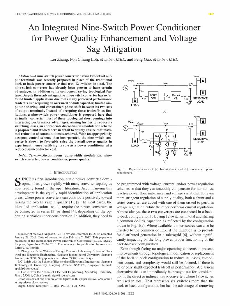
Fig. 4. 120◦-discontinuous references with (a) MS H = MS E = 0.5, ωS H
= ωS E , and (b) MS H = 1× 1.15, MS E = 0.8 × 1.15, ωS H = ωS E .
technically cannot be met by the nine-switch converter. Instead,the nine-switch converter only allows upper dc-rail clampingfor its upper terminals, and lower dc-rail clamping for its lowerterminals, which so far can only be met by the less commonlyadopted 120◦-discontinuous modulation scheme.
To formally demonstrate its suitability, relevant offset andmodified reference expressions for the 120◦-discontinuous mod-ulation scheme are derived, and listed in (2), before plotting themin Fig. 4 for illustration of one phase.
Sinusoidal References⎧⎪⎨⎪⎩
VA = MSH cos(ωSH t + θSH )
VB = MSH cos(ωSH t − 120◦ + θSH )
VC = MSH cos(ωSH t + 120◦ + θSH )⎧⎪⎨⎪⎩
VR = MSE cos(ωSE t + θSE )
VY = MSE cos(ωSE t − 120◦ + θSE )
VW = MSE cos(ωSE t + 120◦ + θSE )
120◦-Discontinuous Modified References
V ′γ = Vγ + VSH , VSH = 1 − max(VA , VB , VC )
γ = A,B, or C
V ′∂ = V∂ + VSE , VSE = −1 − min(VR, VY , VW )
∂ = R, Y, or W (2)
where {MSH , ωSH , θSH } are the modulation ratio, angularfrequency, and initial phase of the shunt terminals, and {MSE ,ωSE , θSE } are the corresponding quantities for the seriesterminals.

1184 IEEE TRANSACTIONS ON POWER ELECTRONICS, VOL. 27, NO. 3, MARCH 2012
Fig. 5. Series control block representation.
Using (2), the modulation plots obtained in Fig. 4 clearlyshow the upper reference tied to only the upper dc-rail andlower reference tied to only the lower dc-rail for a continu-ous duration of 120◦ per fundamental cycle. No crossover ofreferences is observed, implying that the basic modulation rule-of-thumb of the nine-switch converter is not breached, and the120◦-discontinuous scheme is indeed a suitable scheme for re-ducing its commutation count by 33%. Lower commutationcount would then lead to lower switching losses, whose valuesdepend on the current amplitudes and phases at the two terminalsper phase, like all other converters modulated discontinuously.
Before proceeding on to Sections IV-A and IV-B on higherlevel control, it is fair to comment here that a similar modula-tion scheme can be found in [21], whose derivation is orientedmore toward the space vector approach. Surely, the space vec-tor domain can be insightful, but it also needlessly complicatesthe modulation process, and does not bring out the clampingpatterns between the two references per phase as clearly asthe carrier-based approach. The latter is therefore preferred,and has independently been used by the authors to develop the120◦-discontinuous scheme, first presented in [22].
B. Series Control Principles
The series terminals of the nine-switch UPQC are given twocontrol functions that can raise the quality of power suppliedto the load under normal and sag operating conditions. For theformer, the series terminals of the conditioner are tasked to com-pensate for any harmonic distortions that might have originatedat the PCC. Where necessary, they should also help to regu-late the load voltage to compensate for any slight fundamentalvoltage variation. This second functionality is, however, morerelevant under voltage sag condition, where a sizable seriesvoltage (�VSERIES = �V ∗
LOAD − �VSUPPLY ) needs to be injectedto keep the load voltage nearly constant. The overall controlblock representation realized is shown in Fig. 5, where thesubsystem responsible for voltage harmonic compensation isdistinctly identified within the rectangular enclosure.
As seen, the harmonic compensation subsystem is realized byincluding multiple resonant regulators in the stationary frame for
Fig. 6. Bode representation of the selective harmonic regulators found in theseries control scheme.
singling out those prominent low-order load voltage harmonics,including the 5th, 7th, 11th, and 13th components, for elimina-tion. Transfer functions representing these resonant regulatorsHn (s) and their illustration in the Bode diagram are given in (3)and Fig. 6, respectively [23]
Hn (s) = 2KI ωcs + ωc
s2 + 2ωcs + ω2n + ω2
c
(3)
where KI , ωn , and ωc represent the gain parameter, chosenharmonic resonant frequency, and cutoff frequency introducedfor raising stability, respectively, but at the expense of slighttransient sluggishness.
From Fig. 6, it is certainly verified that the regulators intro-duce multiple high gain resonant peaks only at those chosenharmonic frequencies, with gains at the other frequencies closeto zero. Selective harmonic compensation is therefore realiz-able, and has the advantage of reducing the burden shoulderedby the power conditioner, given also that not all harmonics in theload voltage error need to be eliminated in the first place [17],[24]. Another advantage gained by realizing the regulators in thestationary frame is linked to the internal model concept, whichhints that a single resonant regulator tuned at a certain frequencycan process both positive- and negative-sequence componentslocated at that frequency [25]. In contrast, if realized in thesynchronous frame, two control paths per harmonic would gen-erally be needed for processing positive- and negative-sequencecomponents separately. Depending on the number of harmonicsconsidered, such separate paths might end up overstressing thecontrol circuit or microcontroller unnecessarily. To avoid theseunwarranted complications, implementation in the stationaryframe is therefore preferred, and would in fact suit the carrier-based modulation scheme presented in Section III-A better.
Upon next detecting the occurrence of voltage sag, the seriescontrol focus should rightfully switch from harmonic compen-sation to fundamental voltage restoration. Spontaneously, theseries modulating reference fed to the pulse-width modulatorwould change from a small harmonic wave pattern to one withfundamental frequency and much larger amplitude, determinedsolely by the extent of voltage sag. This “normal-to-sag” ref-erence transition has earlier been shown in Section II-C to be

ZHANG et al.: INTEGRATED NINE-SWITCH POWER CONDITIONER FOR POWER QUALITY ENHANCEMENT AND VOLTAGE SAG MITIGATION 1185
TABLE IIILOAD VOLTAGE COMPENSATION RESULTS
smooth, so long as the proper higher level control scheme forproducing the demanded series modulating reference is in place.
Moving forward to explain the higher level control opera-tion during sag, Fig. 5 is referred to again, where those sagcompensating blocks shown above the harmonic regulators arenow discussed. Upon analyzing those blocks, the sag compen-sator is noted to have two degrees of control freedom with thefirst primary degree formed by subtracting the PCC voltagefrom the demanded load voltage along the feedforward pathto give �V ∗
LOAD − �VSUPPLY . Feeding forward of control sig-nal is however not capable of compensating for voltage dropsappearing across the filter and transformer. Because of that, asecondary feedback loop is added to act on the load voltageerror, derived by subtracting the load voltage from its refer-ence (�V ∗
LOAD − �VLOAD ). The computed voltage error is thenfed through a PI regulator in the synchronous frame, whoseeffect is to force the steady-state error to zero, and hence com-pensating for those unaccounted voltage drops appearing acrossthe inductive elements.
Note that for the control presented here, the synchronousframe is chosen simply because the load voltage reference canthen be represented by a single dc constant. If frame trans-formation is not preferred, resonant regulator in the stationaryframe [26] can be used instead, so long as three-phase sinusoidsare also used as the load voltage references.
C. Shunt Control Principles
As per previous power conditioners, the shunt terminals ofthe nine-switch power conditioner are programmed to compen-sate for downstream load current harmonics, reactive power,and to balance its shared dc-link capacitive voltage. To realizethese control objectives, an appropriate control scheme is drawnin Fig. 7, where the measured load current is first fed througha high-pass filter in the synchronous frame. The filter blocksfundamental d-axis active component, and passes forward theharmonics and q-axis reactive component for further process-ing. In parallel, a PI regulator is also added to act on the dc-linkvoltage error, forcing it to zero by generating a small d-axis con-trol reference for compensating losses, and hence maintainingthe dc-link voltage constant. The sum of outputs from the filterand PI regulator then forms the control reference for the mea-sured shunt current to track. Upon tracked properly, the sourcecurrent would be sinusoidal, and the load harmonics and reac-tive power would be solely taken care of by the proposed powerconditioner.
Fig. 7. Shunt control block representation.
V. EXPERIMENTAL VERIFICATION
To validate its performance, a nine-switch power conditionerwas implemented in the laboratory, and controlled using adSPACE DS1103 controller card. The dSPACE card was alsoused for the final acquisition of data from multiple channels si-multaneously, while a 4-channel Lecoy digital scope was simplyused for the initial debugging and verification of the dSPACErecorded data, but only four channels at a time. The final hard-ware setup is shown in Fig. 8, where parametric values usedare also indicated. Other features noted from the figure includethe shunt connection of the upper UPQC terminals to the sup-ply side, and the series connection of the lower terminals tothe load side through three single-phase transformers. Reversalof terminal connections for the setup, like upper→series andlower→shunt, was also affected, but was observed to produceno significant differences, as anticipated. For flexible testingpurposes, the setup was also not directly connected to the grid,but was directed to a programmable ac source, whose purposewas to emulate a controllable grid, where harmonics and sagswere conveniently added.
With such flexibility built-in, two distorted cases were pro-grammed with the first having a lower total harmonic distortion(THD) of around 4.18%. This first case, being less severe, rep-resents most modern grids, regulated by grid codes, better. Thesecond case with a higher THD of around 11.43% was includedmainly to show that the nine-switch UPQC can still functionwell in a heavily distorted grid, which might not be common inpractice. Equipped with these two test cases, experiments wereconducted with the shunt compensation scheme shown in Fig. 7always activated, so as to produce the regulated dc-link voltageneeded for overall UPQC operation. The series compensationscheme shown in Fig. 5, on the other hand, was first deactivated,and then activated to produce the two sets of comparative loadvoltage data tabulated in Table III. The data obviously show thatthe proposed nine-switch UPQC is effective in smoothing the

1186 IEEE TRANSACTIONS ON POWER ELECTRONICS, VOL. 27, NO. 3, MARCH 2012
Fig. 8. Experimental setup and parameters used for testing.
Fig. 9. Experimental supply, series injection, and load voltages captured dur-ing normal power conditioning mode.
Fig. 10. Experimental source, shunt injection, and load currents capturedduring normal power conditioning mode.
load voltage, regardless of the extent of low order grid harmonicdistortion introduced.
To strengthen this observation, Fig. 9 shows the supply, seriesinjection, and load voltages for the second test case with ahigher grid THD, and with both series and shunt compensationactivated. The supply voltage is indeed distorted, and wouldappear across the load if series compensation is deactivated andthe transformer is bypassed. The distortion would, however, belargely blocked from propagating to the load, upon activatingthe series compensation scheme with the shunt compensationscheme still kept executing. Example load voltage waveformillustrating this effectiveness can be found at the bottom ofFig. 9.
Roughly, the same results were also obtained when the nine-switch converter was replaced by its back-to-back precedencewith all other system parameters and control schemes kept
ZHANG et al.: INTEGRATED NINE-SWITCH POWER CONDITIONER FOR POWER QUALITY ENHANCEMENT AND VOLTAGE SAG MITIGATION 1187
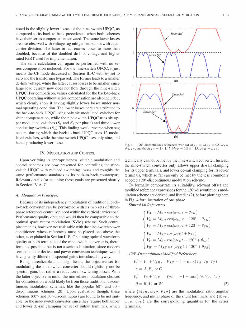
Fig. 11. Experimental supply, series injection, and load voltages during (a) normal-to-sag and (b) sag-to-normal transitions.
unchanged. This finding is certainly expected, since both con-verters differ only by their high frequency switching harmon-ics produced, which will not be prominent in those filteredquantities of interest, shown in Table III and Fig. 9. Produc-ing the same results is however still an advantage for thenine-switch converter, since it achieves that with three lessersemiconductor switches, and hence a lower system cost. Tonext verify its shunt compensating ability, Fig. 10 shows thesource, shunt injection and load currents conditioned by thenine-switch UPQC. Although the load current is heavily dis-torted, the shunt control scheme in Fig. 7 is capable of compen-
sating it, so that the grid current drawn is always sinusoidal, asintended.
With the programmable source now configured to introducea 20% sag, Fig. 11 shows the correspondingly sagged grid volt-age, series injection voltage, and compensated load voltage dur-ing the normal to sag transition and its inverse recovery. Thesewaveforms collectively prove that the sag has been blockedfrom propagating to the load, while yet using lesser semicon-ductor switches. Complementing, Fig. 12 shows the grid, shuntinjection, and load currents during the same normal to sag tran-sition and its recovery. The grid current is obviously sinusoidal

1188 IEEE TRANSACTIONS ON POWER ELECTRONICS, VOL. 27, NO. 3, MARCH 2012
Fig. 12. Experimental grid, shunt injection, and load currents during (a) normal-to-sag and (b) sag-to-normal transitions.
throughout the whole transitional process with an increase inamplitude noted during the period of grid sag. This increasein grid current is transferred to the shunt terminal of the nine-switch power conditioner, whose absorbed (negative of injected)current now has a prominent fundamental component, as alsoreflected by the second row of waveforms plotted in Fig. 12.Upon processed by the nine-switch power stage, the incremen-tal power associated with the higher shunt current is eventuallyforced out of the series terminal as an injected voltage, neededfor keeping the load voltage and power unchanged.
Yet another feature verified through the testing is the dc-linkvoltage needed by the nine-switch power conditioner, whosevalue is always higher than that of the back-to-back conditioner,if series compensation is demanded. This increase can, however,be kept small by adopting the carrier division scheme shown inFig. 3. To confirm that, Fig. 13 shows the conditioner dc-linkvoltage regulated at only 270 V throughout the whole sag andrecovery process. This dc-link voltage is merely 8% higher thanthat of the back-to-back case, hence verifying those theoreticalreasoning discussed in Sections II-C and III.

ZHANG et al.: INTEGRATED NINE-SWITCH POWER CONDITIONER FOR POWER QUALITY ENHANCEMENT AND VOLTAGE SAG MITIGATION 1189
Fig. 13. Experimental dc-link voltage during (a) normal-to-sag and (b) sag-to-normal transitions.
VI. CONCLUSION
This paper evaluates shortcomings experienced by previousapplications of the newly proposed nine-switch converter. Witha better understanding developed, the conclusion drawn is thatthe nine-switch converter is not an attractive alternative for re-placing back-to-back converter with two shunt bridges. Instead,the nine-switch converter is more suitable for replacing back-to-back converter in “series–shunt” systems, where one goodexample is the UPQC. As a further performance booster, amodified 120◦-discontinuous modulation scheme is presentedfor reducing the overall commutation count by 33%. Followedup next with proper shunt and series control, harmonics, reac-tive power, and voltage sags are compensated promptly with noappreciable degradation in performance. The nine-switch condi-tioner is therefore proved to be effective, while yet using lessersemiconductor switches. Experimental results for confirmingits anticipated smooth performance have already been obtainedthrough intensive laboratory testing.
REFERENCES
[1] D. L. Ashcroft, “The static power converter committee—Some perspec-tives,” IEEE Trans. Ind. Applicat., vol. IA-21, no. 5, pp. 1097–1098, Sep.1985.
[2] B. Han, B. Bae, H. Kim, and S. Baek, “Combined operation of uni-fied power-quality conditioner with distributed generation,” IEEE Trans.Power Delivery, vol. 21, no. 1, pp. 330–338, Jan. 2006.
[3] H. Johal and D. Divan, “Design considerations for series-connected dis-tributed FACTS converters,” IEEE Trans. Ind. Applicat., vol. 43, no. 6,pp. 1609–1618, Nov./Dec. 2007.
[4] T. L. Lee, J. C. Li, and P. T. Cheng, “Discrete frequency tuning active filterfor power system harmonics,” IEEE Trans. Power Electron., vol. 24, no. 5,pp. 1209–1217, May 2009.
[5] V. Khadkikar and A. Chandra, “A new control philosophy for a uni-fied power quality conditioner (UPQC) to coordinate load-reactive powerdemand between shunt and series inverters,” IEEE Trans. Power Del.,vol. 23, no. 4, pp. 2522–2534, Oct. 2008.
[6] Y. , W. Li, D. M. Vilathgamuwa, and P. C. Loh, “A grid-interfacing powerquality compensator for three-phase three-wire microgrid applications,”IEEE Trans. Power Electron., vol. 21, no. 4, pp. 1021–1031, Jul. 2006.
[7] J. W. Kolar, F. Schafmeister, S. D. Round, and H. Ertl, “Novel three-phaseac–ac sparse matrix converters,” IEEE Trans. Power Electron., vol. 22,no. 5, pp. 1649–1661, Sep. 2007.
[8] P. C. Loh, F. Blaabjerg, F. Gao, A. Baby, and D. A. C. Tan, “Pulsewidthmodulation of neutral-point-clamped indirect matrix converter,” IEEETrans. Ind. Applicat., vol. 44, no. 6, pp. 1805–1814, Nov./Dec. 2008.
[9] F. Blaabjerg, S. Freysson, H. H. Hansen, and S. Hansen, “A new op-timized space-vector modulation strategy for a component-minimizedvoltage source inverter,” IEEE Trans. Power Electron., vol. 12, no. 4,pp. 704–714, Jul. 1997.
[10] E. Ledezma, B. McGrath, A. Munoz, and T. A. Lipo, “Dual ac-drivesystem with a reduced switch count,” IEEE Trans. Ind. Applicat., vol. 37,no. 5, pp. 1325–1333, Sep./Oct. 2001.
[11] M. Jones, S. N. Vukosavic, D. Dujic, E. Levi, and P. Wright, “Five-leginverter PWM technique for reduced switch count two-motor constantpower applications,” IET Proc. Electric Power Applicat., vol. 2, no. 5,pp. 275–287, Sep. 2008.
[12] C. Liu, B. Wu, N. R. Zargari, D. Xu, and J. Wang, “A novel three-phase three-leg ac/ac converter using nine IGBTs,” IEEE Trans. PowerElectron., vol. 24, no. 5, pp. 1151–1160, May 2009.
[13] T. Kominami and Y. Fujimoto, “A novel three-phase inverter for indepen-dent control of two three-phase loads,” in Proc. IEEE-Ind. Applicat. Soc.(IAS)s, 2007, pp. 2346–2350.
[14] T. Kominami and Y. Fujimoto, “Inverter with reduced switching-devicecount for independent ac motor control,” in Proc. IEEE-IECON, 2007,pp. 1559–1564.
[15] C. Liu, B. Wu, N. R. Zargari, and D. Xu, “A novel nine-switch PWMrectifier-inverter topology for three-phase UPS applications,” in Proc.IEEE-Everyday Practical Electron. (EPE), 2007, pp. 1–10.
[16] S. M. Dehghan, M. Mohamadian, and A. Yazdian, “Hybrid electric vehiclebased on bidirectional Z-source nine-switch inverter,” IEEE Trans. Veh.Technol., vol. 59, no. 6, pp. 2641–2653, Jul. 2010.
[17] M. , J. Newman, D. G. Holmes, J. G. Nielsen, and F. Blaabjerg, “A dynamicvoltage restorer (DVR) with selective harmonic compensation at mediumvoltage level,” IEEE Trans. Ind. Applicat., vol. 41, no. 6, pp. 1744–1753,Nov./Dec. 2005.
[18] M. J. Newman and D. G. Holmes, “A universal custom power conditioner(UCPC) with selective harmonic voltage compensation,” in Proc. IEEE-IECON, 2002, pp. 1261–1266.
[19] Y. Li, D. M. Vilathgamuwa, and P. C. Loh, “Microgrid power quality en-hancement using a three-phase four-wire grid-interfacing compensator,”IEEE Trans. Ind. Applicat., vol. 41, no. 6, pp. 1707–1719, Nov./Dec. 2005.
[20] O. Ojo, “The generalized discontinuous PWM scheme for three-phasevoltage source inverters,” IEEE Trans. Ind. Electron., vol. 51, no. 6,pp. 1280–1289, Dec. 2004.
[21] S. M. D. Dehnavi, M. Mohamadian, A. Yazdian, and F. Ashrafzadeh,“Space vectors modulation for nine-switch converters,” IEEE Trans.Power Electron., vol. 25, no. 6, pp. 1488–1496, Jun. 2010.
[22] F. Gao, L. Zhang, D. Li, P. , C. Loh, Y. Tang, and H. Gao, “Optimalpulsewidth modulation of nine-switch converter,” IEEE Trans. PowerElectron., vol. 25, no. 9, pp. 2331–2343, Sep. 2010.
[23] D. N. Zmood, D. G. Holmes, and G. H. Bode, “Frequency-domain analysisof three-phase linear current regulators,” IEEE Trans. Ind. Appl., vol. 37,no. 2, pp. 601–610, Mar./Apr. 2001.

1190 IEEE TRANSACTIONS ON POWER ELECTRONICS, VOL. 27, NO. 3, MARCH 2012
[24] P. Mattavelli, “Closed-loop selective harmonic compensation for activefilters,” IEEE Trans. Ind. Appl., vol. 37, no. 1, pp. 81–89, Jan./Feb. 2001.
[25] R. Teodorescu, F. Blaabjerg, M. Liserre, and P. C. Loh, “Proportional-resonant controllers and filters for grid-connected voltage-source convert-ers,” IEE Proc. Electric Power Applicat., vol. 153, no. 5, pp. 750–762,Sep. 2006.
[26] D. N. Zmood and D. G. Holmes, “Stationary frame current regulationof PWM inverters with zero steady-state error,” IEEE Trans. PowerElectron., vol. 18, no. 3, pp. 814–822, May 2003.
Lei Zhang received the Bachelor’s degree in elec-trical engineering in 2007 from Wuhan Univer-sity, Wuhan, China. From 2007 to 2008, he stud-ied in Power Engineering in Chalmers University ofTechnology, Gothenburg, Sweden. Currently, he isworking toward the Ph.D. degree from the Schoolof Electrical and Electronic Engineering, NanyangTechnological University, Singapore.
From July to October in 2009, he was a Visit-ing Scholar in the Institute of Energy Technology,Aalborg University, Denmark, where he worked on
the HVdc system in RTDS simulator. His research field includes distributedcontrol of multiple converters, renewable technology, and converter design.
Poh Chiang Loh (S’01–M’04) received the B.Eng.(Hons.) and M.Eng. degrees from the National Uni-versity of Singapore in 1998 and 2000, respec-tively, and the Ph.D. degree from Monash University,Australia, in 2002, all in electrical engineering.
During the summer of 2001, he was a Visit-ing Scholar with the Wisconsin Electric Machineand Power Electronics Consortium, University ofWisconsin-Madison, Madison, where he worked onthe synchronized implementation of cascaded multi-level inverters, and reduced common mode carrier-
based and hysteresis control strategies for multilevel inverters. From 2002 to2003, he was a Project Engineer with the Defence Science and TechnologyAgency, Singapore, managing major defence infrastructure projects and explor-ing new technology for defence applications. From 2003 to 2009, he was anAssistant Professor with the Nanyang Technological University, Singapore, andsince 2009, he has been an Associate Professor at the same university. In 2005,he has been a Visiting Staff first at the University of Hong Kong, and then atAalborg University, Denmark. In 2007 and 2009, he again returned to AalborgUniversity first as a Visiting Staff working on matrix converters and the controlof grid-interfaced inverters, and then as a Guest Member of the Vestas PowerProgram.
Dr. Loh has received two-third paper prizes from the IEEE-IAS IPCC com-mittee in 2003 and 2006, and he is now serving as an Associate Editor of theIEEE TRANSACTIONS ON POWER ELECTRONICS.
Feng Gao (S’07–M’09) received the B.Eng. andM.Eng. degrees in electrical engineering fromShandong University, Jinan, China, in 2002 and 2005,respectively, and the Ph.D. degree from the Schoolof Electrical and Electronic Engineering, NanyangTechnological University, Singapore, in 2009.
From 2008 to 2009, he was a Research Fel-low in Nanyang Technological University. Since2010, he joined the School of Electrical Engineering,Shandong University, where he is currently a Profes-sor. From September 2006 to February 2007, he was
a Visiting Scholar at the Institute of Energy Technology, Aalborg University,Aalborg, Denmark.
Dr. Gao was the recipient of the IEEE Industry Applications Society Indus-trial Power Converter Committee Prize for a paper published in 2006.
Related Documents