1FEATURES TMS470R1A384 www.ti.com ......................................................................................................................................................... SPNS110E –AUGUST 2005–REVISED MAY 2008 16/32-Bit RISC Flash Microcontroller 23• High-Performance Static CMOS Technology – Two Serial Communication Interfaces (SCIs) • TMS470R1x 16/32-Bit RISC Core (ARM7TDMI™) – 2 24 Selectable Baud Rates – 24-MHz System Clock (48-MHz Pipeline) – Asynchronous/Isosynchronous Modes – Independent 16/32-Bit Instruction Set – Two Standard CAN Controllers (SCC) – Open Architecture With Third-Party Support – 16-Mailbox Capacity – Built-In Debug Module – Fully Compliant With CAN Protocol, Version 2.0B • Integrated Memory – Class II Serial Interface B (C2SIb) – 384K-Byte Program Flash – Normal 10.4 Kbps and 4X Mode – Three Banks With 18 Contiguous 41.6 Kbps Sectors – Three Inter-Integrated Circuit (I2C) Modules – 32K-Byte Static RAM (SRAM) (See I2C Notes in TMS470R1A384 Silicon • Operating Features Errata, Literature Number SPNZ148) – Core Supply Voltage (V CC ): 1.71 V to 2.05 V – Multi-Master and Slave Interfaces – I/O Supply Voltage (V CCIO ): 3.0 V to 3.6 V – Up to 400 Kbps (Fast Mode) – Low-Power Modes: STANDBY and HALT – 7- and 10-Bit Address Capability – Extended Industrial Temperature Range • High-End Timer (HET) • 470+ System Module – 12 Programmable I/O Channels: – 32-Bit Address Space Decoding – 12 High-Resolution Pins – Bus Supervision for Memory/Peripherals – High-Resolution Share Feature (XOR) – Analog Watchdog (AWD) Timer – High-End Timer RAM – Enhanced Real-Time Interrupt (RTI) – 64-Instruction Capacity – Interrupt Expansion Module (IEM) • External Clock Prescale (ECP) Module – System Integrity and Failure Detection – Programmable Low-Frequency External • Direct Memory Access (DMA) Controller Clock (CLK) – 32 Control Packets and 16 Channels • 12-Channel 10-Bit Multi-Buffered • Zero-Pin Phase-Locked Loop (ZPLL)-Based Analog-to-Digital Converter (MibADC) Clock Module With Prescaler – 32-Word FIFO Buffer – Multiply-by-4 or -8 Internal ZPLL Option – Single- or Continuous-Conversion Modes – ZPLL Bypass Mode – 1.55-μs Minimum Sample/Conversion Time • Expansion Bus Module (EBM) (PGE Package) – Calibration Mode and Self-Test Features – Supports 8- and 16-Bit Expansion Bus • 55 Dedicated General-Purpose I/O (GIO) Pins Memory Interface Mappings and 39 Additional Peripheral I/Os (PGE) – 40 I/O Expansion Bus Pins • 14 Dedicated General-Purpose I/O (GIO) Pins • Ten Communication Interfaces: and 39 Additional Peripheral I/Os (PZ) – Two Serial Peripheral Interfaces (SPIs) • Flexible Interrupt Handling – 255 Programmable Baud Rates • Eight External Interrupts 1 Please be aware that an important notice concerning availability, standard warranty, and use in critical applications of Texas Instruments semiconductor products and disclaimers thereto appears at the end of this data sheet. 2ARM7TDMI is a trademark of Advanced RISC Machines Limited (ARM). 3All other trademarks are the property of their respective owners. PRODUCTION DATA information is current as of publication date. Copyright © 2005–2008, Texas Instruments Incorporated Products conform to specifications per the terms of the Texas Instruments standard warranty. Production processing does not necessarily include testing of all parameters.

Welcome message from author
This document is posted to help you gain knowledge. Please leave a comment to let me know what you think about it! Share it to your friends and learn new things together.
Transcript
1FEATURES
TMS470R1A384
www.ti.com ......................................................................................................................................................... SPNS110E–AUGUST 2005–REVISED MAY 2008
16/32-Bit RISC Flash Microcontroller
23• High-Performance Static CMOS Technology – Two Serial Communication Interfaces(SCIs)• TMS470R1x 16/32-Bit RISC Core
(ARM7TDMI™) – 224 Selectable Baud Rates– 24-MHz System Clock (48-MHz Pipeline) – Asynchronous/Isosynchronous Modes– Independent 16/32-Bit Instruction Set – Two Standard CAN Controllers (SCC)– Open Architecture With Third-Party Support – 16-Mailbox Capacity– Built-In Debug Module – Fully Compliant With CAN Protocol,
Version 2.0B• Integrated Memory– Class II Serial Interface B (C2SIb)– 384K-Byte Program Flash
– Normal 10.4 Kbps and 4X Mode– Three Banks With 18 Contiguous41.6 KbpsSectors
– Three Inter-Integrated Circuit (I2C) Modules– 32K-Byte Static RAM (SRAM)(See I2C Notes in TMS470R1A384 Silicon• Operating FeaturesErrata, Literature Number SPNZ148)
– Core Supply Voltage (VCC): 1.71 V to 2.05 V– Multi-Master and Slave Interfaces
– I/O Supply Voltage (VCCIO): 3.0 V to 3.6 V– Up to 400 Kbps (Fast Mode)
– Low-Power Modes: STANDBY and HALT– 7- and 10-Bit Address Capability
– Extended Industrial Temperature Range• High-End Timer (HET)
• 470+ System Module– 12 Programmable I/O Channels:
– 32-Bit Address Space Decoding– 12 High-Resolution Pins
– Bus Supervision for Memory/Peripherals– High-Resolution Share Feature (XOR)
– Analog Watchdog (AWD) Timer– High-End Timer RAM
– Enhanced Real-Time Interrupt (RTI)– 64-Instruction Capacity
– Interrupt Expansion Module (IEM)• External Clock Prescale (ECP) Module
– System Integrity and Failure Detection– Programmable Low-Frequency External
• Direct Memory Access (DMA) Controller Clock (CLK)– 32 Control Packets and 16 Channels • 12-Channel 10-Bit Multi-Buffered
• Zero-Pin Phase-Locked Loop (ZPLL)-Based Analog-to-Digital Converter (MibADC)Clock Module With Prescaler – 32-Word FIFO Buffer– Multiply-by-4 or -8 Internal ZPLL Option – Single- or Continuous-Conversion Modes– ZPLL Bypass Mode – 1.55-µs Minimum Sample/Conversion Time
• Expansion Bus Module (EBM) (PGE Package) – Calibration Mode and Self-Test Features– Supports 8- and 16-Bit Expansion Bus • 55 Dedicated General-Purpose I/O (GIO) Pins
Memory Interface Mappings and 39 Additional Peripheral I/Os (PGE)– 40 I/O Expansion Bus Pins • 14 Dedicated General-Purpose I/O (GIO) Pins
• Ten Communication Interfaces: and 39 Additional Peripheral I/Os (PZ)– Two Serial Peripheral Interfaces (SPIs) • Flexible Interrupt Handling
– 255 Programmable Baud Rates • Eight External Interrupts
1
Please be aware that an important notice concerning availability, standard warranty, and use in critical applications ofTexas Instruments semiconductor products and disclaimers thereto appears at the end of this data sheet.
2ARM7TDMI is a trademark of Advanced RISC Machines Limited (ARM).3All other trademarks are the property of their respective owners.
PRODUCTION DATA information is current as of publication date. Copyright © 2005–2008, Texas Instruments IncorporatedProducts conform to specifications per the terms of the TexasInstruments standard warranty. Production processing does notnecessarily include testing of all parameters.
HET[1]HET[2]
VCCIO
GIOE[6]
HET[4]HET[3]GIOE[5]VSS
GIOE[2]SPI2SOMI
SPI2ENASPI2SIMO
GIOE[3]SPI2SCSHET[5]GIOE[4]
GIOD[0]GIOH[1]
SCI2RX
SCI1RX
GIOE[0]GIOB[0]
SCI1TX
SCI1CLKGIOE[1]
SCI2TX
VSSSCI2CLK
VCC
CAN2SRXCAN2STXSPI2CLK
GIOD[1]
GIOH[4]GIOH[3]
GIOH[2]
727170696867666564636261605958575655545352515049484746454443424140393837
109110111112113114115116117118119120121122123124125126127128129130131132133134135136137138139140141142143144
ADREFHIADREFLO
VCCADVSSAD
ADIN[4]ADIN[3]ADIN[2]ADIN[1]ADIN[0]
PORRSTGIOC[4]GIOC[3]
RSTVSSVCC
TESTGIOH[5]GIOC[2]
GIOA[4]/INT[4]GIOC[1]
VSSVCC
VCCPFLTP2
GIOA[3]/INT[3]GIOA[2]/INT[2]
GIOC[0]GIOA[1]/INT[1]/ECLK
VCCIOVSS
GIOH[0]GIOG[7]
GIOA[0]/INT[0]GIOG[6]GIOG[5]
TRST
AD
IN[5
]A
DIN
[6]
AD
IN[7
]A
DIN
[8]
AD
IN[9
]A
DIN
[10]
AD
IN[1
1]A
DE
VT
GIO
F[7
]G
IOF
[6]
GIO
A[5
]/IN
T[5
]P
LL
DIS
GIO
F[5
]I2
C2S
CL
I2C
2SD
AG
IOF
[4]
VC
CV
SS
GIO
F[3
]G
IOF
[2]
I2C
1SC
LI2
C1S
DA
VC
CIO
VS
SC
AN
1ST
XC
AN
1SR
XG
IOF
[1]
CL
KO
UT
GIO
F[0
]G
IOA
[7]/
INT
[7]
GIO
A[6
]/IN
T[6
]G
IOE
[7]
TC
KT
DO
TD
IH
ET
[0]
108
107
106
105
104
103
102
101
100 99 98 97 96 95 94 93 92 91 90 89 88 87 86 85 84 83 82 81 80 79 78 77 76 75 74 73
1 2 3 4 5 6 7 8 9
SP
I1S
CS
SP
I1E
NA
GIO
G[4
]S
PI1
CL
KS
PI1
SIM
OG
IOG
[3]
SP
I1S
OM
IG
IOG
[2]
HE
T[6
]10 11 12 13 14 15 16 17 18 19 20 21
GIO
G[1
]H
ET
[7]
HE
T[8
]V
CC
VS
SH
ET
[18]
TM
S2
TM
SH
ET
[20]
HE
T[2
2]G
IOG
[0]
C2S
ILP
N22 23 24 25 26 27 28 29 30 31 32 33
C2S
IRX
GIO
D[5
]C
2SIT
XV
CC
IOV
SS
GIO
D[4
]I2
C3S
CL
I2C
3SD
AG
IOD
[3]
VC
CO
SC
OU
TO
SC
IN34 35 36
VS
SG
IOD
[2]
AW
D
TMS470R1A384
SPNS110E–AUGUST 2005–REVISED MAY 2008 ......................................................................................................................................................... www.ti.com
• On-Chip Scan-Base Emulation Logic, IEEE • 100-Pin Plastic Low-Profile Quad FlatpackStandard 1149.1(1) (JTAG) Test-Access Port (PZ Suffix)
• 144-Pin Plastic Low-Profile Quad Flatpack (1) The test-access port is compatible with the IEEE Standard1149.1-1990, IEEE Standard Test-Access Port and Boundary(PGE Suffix)Scan Architecture specification. Boundary scan is notsupported on this device.
TMS470R1A384 144-Pin PGE Package (Top View) (Without Expansion Bus)
2 Submit Documentation Feedback Copyright © 2005–2008, Texas Instruments Incorporated
Product Folder Link(s): TMS470R1A384
HET[1]HET[2]
VCCIO
EBDATA[6]
HET[4]HET[3]EBDATA[5]VSS
EBDATA[2]SPI2SOMI
SPI2ENASPI2SIMO
EBDATA[3]SPI2SCSHET[5]EBDATA[4]
EBADDR[0]EBADDR[23]/EBADDR[15]
SCI2RX
SCI1RX
EBDATA[0]EBDMAREQ[0]
SCI1TX
SCI1CLKEBDATA[1]
SCI2TX
VSSSCI2CLK
VCC
CAN2SRXCAN2STXSPI2CLK
EBADDR[1]
EBADDR[26]/EBADDR[18]EBADDR[25]/EBADDR[17]
EBADDR[24]/EBADDR[16]
727170696867666564636261605958575655545352515049484746454443424140393837
109110111112113114115116117118119120121122123124125126127128129130131132133134135136137138139140141142143144
ADREFHIADREFLO
VCCADVSSAD
ADIN[4]ADIN[3]ADIN[2]ADIN[1]ADIN[0]
PORRSTEBCS[6]EBCS[5]
RSTVSSVCC
TESTEBHOLDEBWR[1]
GIOA[4]/INT[4]EBWR[0]
VSSVCC
VCCPFLTP2
GIOA[3]/INT[3]GIOA[2]/INT[2]
EBOEGIOA[1]/INT[1]/ECLK
VCCIOVSS
EBADDR[22]/EBADDR[14]EBADDR[21]/EBADDR[13]
GIOA[0]/INT[0]EBADDR[20]/EBADDR[12]EBADDR[19]/EBADDR[11]
TRST
AD
IN[5
]A
DIN
[6]
AD
IN[7
]A
DIN
[8]
AD
IN[9
]A
DIN
[10]
AD
IN[1
1]A
DE
VT
EB
AD
DR
[13]
/EB
DA
TA[1
5]E
BA
DD
R[1
2]/E
BD
ATA
[14]
GIO
A[5
]/IN
T[5
]P
LL
DIS
EB
AD
DR
[11]
/EB
DA
TA[1
3]I2
C2S
CL
I2C
2SD
AE
BA
DD
R[1
0]/E
BD
ATA
[12]
VC
CV
SS
EB
AD
DR
[9]/
EB
DA
TA[1
1]E
BA
DD
R[8
]/E
BD
ATA
[10]
I2C
1SC
LI2
C1S
DA
VC
CIO
VS
SC
AN
1ST
XC
AN
1SR
XE
BA
DD
R[7
]/E
BD
ATA
[9]
CL
KO
UT
EB
AD
DR
[6]/
EB
DA
TA[8
]G
IOA
[7]/
INT
[7]
GIO
A[6
]/IN
T[6
]E
BD
ATA
[7]
TC
KT
DO
TD
IH
ET
[0]
108
107
106
105
104
103
102
101
100
99 98 97 96 95 94 93 92 91 90 89 88 87 86 85 84 83 82 81 80 79 78 77 76 75 74 73
1 2 3 4 5 6 7 8 9
SP
I1S
CS
SP
I1E
NA
EB
AD
DR
[18]
/EB
AD
DR
[10]
SP
I1C
LK
SP
I1S
IMO
EB
AD
DR
[17]
/EB
AD
DR
[9]
SP
I1S
OM
IE
BA
DD
R[1
6]/E
BA
DD
R[8
]H
ET
[6]
10 11 12 13 14 15 16 17 18 19 20 21
EB
AD
DR
[15]
/EB
AD
DR
[7]
HE
T[7
]H
ET
[8]
VC
CV
SS
HE
T[1
8]T
MS
2T
MS
HE
T[2
0]H
ET
[22]
EB
AD
DR
[14]
/EB
AD
DR
[6]
C2S
ILP
N22 23 24 25 26 27 28 29 30 31 32 33
C2S
IRX
EB
AD
DR
[5]
C2S
ITX
VC
CIO
VS
SE
BA
DD
R[4
]I2
C3S
CL
I2C
3SD
AE
BA
DD
R[3
]V
CC
OS
CO
UT
OS
CIN
34 35 36
VS
SE
BA
DD
R[2
]A
WD
TMS470R1A384
www.ti.com ......................................................................................................................................................... SPNS110E–AUGUST 2005–REVISED MAY 2008
TMS470R1A384 144-Pin PGE Package (Top View) (with Expansion Bus)
Copyright © 2005–2008, Texas Instruments Incorporated Submit Documentation Feedback 3
Product Folder Link(s): TMS470R1A384
1 2 3 4 5 6 7 8 9 10 11 12 1413 15 16 2017 18 19 2221 23 2524
75 74 73 72 71 70 6869 67 66 6465 6263 61 60 565859 57 5455 53 5152
50494847464544434241403938373635343332313029282726
767778798081828384858687888990919293949596979899100
ADREFHIADREFLO
VCCADVSSAD
ADIN[4]ADIN[3]ADIN[2]ADIN[1]ADIN[0]
PORRSTRST
TESTGIOH[5]
GIOA[4]/INT[4]VSSVCC
VCCPFLTP2
GIOA[3]/INT[3]GIOA[2]/INT[2]
GIOA[1]/INT[1]/ECLKVCCIO
VSSGIOA[0]/INT[0]
TRST
HET[1]HET[2]VCCIOVSSHET[3]HET[4]HET[5]SPI2SCSSPI2ENASPI2SIMOSPI2SOMISPI2CLKCAN2STXCAN2SRXSCI2CLKSCI2RXSCI2TXSCI1CLKSCI1RXSCI1TXGIOB[0]GIOH[1]GIOH[2]GIOH[3]GIOH[4]
AD
IN[5
]A
DIN
[6]
AD
IN[7
]A
DIN
[8]
AD
IN[9
]A
DIN
[10]
AD
IN[1
1]A
DE
VT
GIO
A[5
]/IN
T[5
]P
LL
DIS
I2C
2SC
LI2
C2S
DA
VC
CV
SS
I2C
1SC
LI2
C1S
DA
CA
N1S
TX
CA
N1S
RX
CL
KO
UT
GIO
A[7
]/IN
T[7
]G
IOA
[6]/
INT
[6]
TC
KT
DO
TD
IH
ET
[0]
SP
I1S
CS
SP
I1E
NA
SP
I1C
LK
SP
I1S
IMO
SP
I1S
OM
IH
ET
[6]
HE
T[7
]H
ET
[8]
HE
T[1
8]T
MS
2T
MS
HE
T[2
0]H
ET
[22]
C2S
ILP
NC
2SIR
XC
2SIT
XV
CC
IOV
SS
I2C
SC
LI2
C3S
DA
VC
CO
SC
OU
TO
SC
INV
SS
AW
D
TMS470R1A384
SPNS110E–AUGUST 2005–REVISED MAY 2008 ......................................................................................................................................................... www.ti.com
TMS470R1A384 100-Pin PZ Package (Top View)
4 Submit Documentation Feedback Copyright © 2005–2008, Texas Instruments Incorporated
Product Folder Link(s): TMS470R1A384
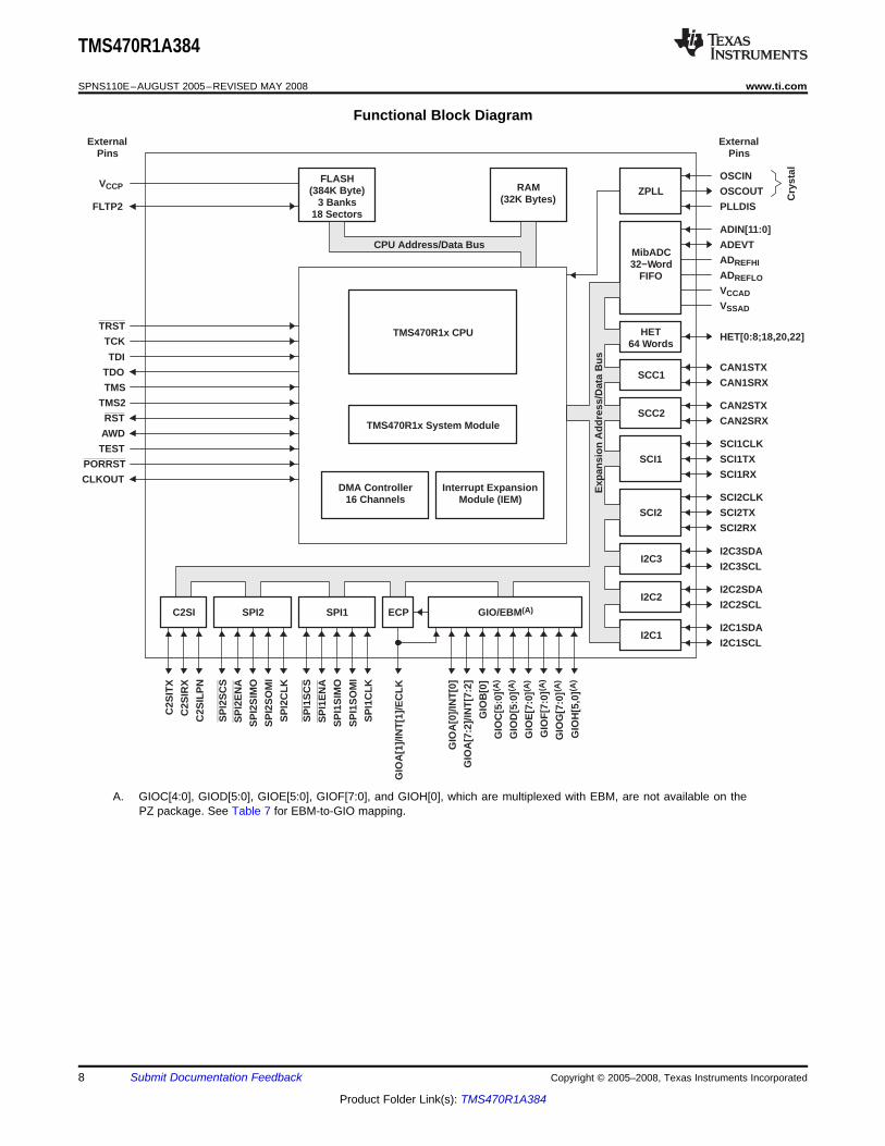
DESCRIPTION
TMS470R1A384
www.ti.com ......................................................................................................................................................... SPNS110E–AUGUST 2005–REVISED MAY 2008
The TMS470R1A384 (1) devices are members of the Texas Instruments TMS470R1x family of general-purpose16/32-bit reduced instruction set computer (RISC) microcontrollers. The A384 microcontroller offers highperformance utilizing the high-speed ARM7TDMI 16/32-bit RISC central processing unit (CPU), resulting in ahigh instruction throughput while maintaining greater code efficiency. The ARM7TDMI 16/32-bit RISC CPU viewsmemory as a linear collection of bytes numbered upwards from zero. The A384 utilizes the big-endian formatwhere the most significant byte of a word is stored at the lowest-numbered byte and the least significant byte atthe highest-numbered byte.
High-end embedded control applications demand more performance from their controllers while maintaining lowcosts. The A384 RISC core architecture offers solutions to these performance and cost demands whilemaintaining low power consumption.
The A384 devices contain the following:• ARM7TDMI 16/32-bit RISC CPU• TMS470R1x system module (SYS) with 470+ enhancements• 384K-byte flash• 32K-byte SRAM• Zero-pin phase-locked loop (ZPLL) clock module• Analog watchdog (AWD) timer• Enhanced real-time interrupt (RTI) module• Interrupt expansion module (IEM)• Two serial peripheral interface (SPI) modules• Two serial communications interface (SCI) modules• Two standard CAN controllers (SCC)• Three inter-integrated circuit (I2C) modules• Class II serial interface B (C2SIb) module• 10-bit multi-buffered analog-to-digital converter (MibADC), with 12 input channels• High-end timer (HET) controlling 12 I/Os• External clock prescale (ECP)• Expansion bus module (EBM)• Up to 87 I/O pins and 1 input-only pin (PGE suffix only), up to 51 I/O pins and 1 input-only pin (PZ suffix only)
The functions performed by the 470+ system module (SYS) include:• Address decoding• Memory protection• Memory and peripherals bus supervision• Reset and abort exception management• Prioritization for all internal interrupt sources• Device clock control• Parallel signature analysis (PSA)
The enhanced real-time interrupt (RTI) module on the A384 has the option to be driven by the oscillator clock.This data sheet includes device-specific information such as memory and peripheral select assignment, interruptpriority, and a device memory map. For a more detailed functional description of the SYS module, see theTMS470R1x System Module Reference Guide (literature number SPNU189).
The A384 memory includes general-purpose SRAM supporting single-cycle read/write accesses in byte,half-word, and word modes.
The flash memory on this device is a nonvolatile, electrically erasable and programmable memory implementedwith a 32-bit-wide data bus interface. The flash operates with a system clock frequency of up to 24 MHz. Whenin pipeline mode, the flash operates with a system clock frequency of up to 48 MHz. For more detailedinformation on the flash, see the Flash section of this data sheet and the TMS470R1x F05 Flash ReferenceGuide (literature number SPNU213).(1) Throughout the remainder of this document, the TMS470R1A384 is referred to as either the full device name or as A384.
Copyright © 2005–2008, Texas Instruments Incorporated Submit Documentation Feedback 5
Product Folder Link(s): TMS470R1A384
TMS470R1A384
SPNS110E–AUGUST 2005–REVISED MAY 2008 ......................................................................................................................................................... www.ti.com
The A384 device has ten communication interfaces: two SPIs, two SCIs, two SCCs, a C2SI, and three I2Cs. TheSPI provides a convenient method of serial interaction for high-speed communications between similarshift-register type devices. The SCI is a full-duplex, serial I/O interface intended for asynchronous communicationbetween the CPU and other peripherals using the standard non-return-to-zero (NRZ) format. The SCC uses aserial, multimaster communication protocol that efficiently supports distributed real-time control with robustcommunication rates of up to 1 megabit per second (Mbps). The SCC is ideal for applications operating in noisyand harsh environments (e.g., industrial fields) that require reliable serial communication or multiplexed wiring.The C2SIb allows the A384 to transmit and receive messages on a class II network following an SAE J1850 (2)
standard. The I2C module is a multi-master communication module providing an interface between the A384microcontroller and an I2C-compatible device via the I2C serial bus. The I2C supports both 100 Kbps and400 Kbps speeds. For more detailed functional information on the SPI, SCI, and CAN peripherals, see thespecific reference guides (literature numbers SPNU195, SPNU196, and SPNU197). For more detailed functionalinformation on the I2C, see the TMS470R1x Inter-Integrated Circuit (I2C) Reference Guide (literature numberSPNU223). For more detailed functional information on the C2SI, see the TMS470R1x Class II Serial Interface B(C2SIb) Reference Guide (literature number SPNU214).
The HET is an advanced intelligent timer that provides sophisticated timing functions for real-time applications.The timer is software-controlled, using a reduced instruction set, with a specialized timer micromachine and anattached I/O port. The HET can be used for compare, capture, or general-purpose I/O. It is especially well suitedfor applications requiring multiple sensor information and drive actuators with complex and accurate time pulses.The HET used in this device is the high-end timer lite. It has fewer I/Os than the usual 32 in a standard HET. Formore detailed functional information on the HET, see the TMS470R1x High-End Timer (HET) Reference Guide(literature number SPNU199).
The A384 HET peripheral contains the XOR-share feature. This feature allows two adjacent HET high- resolutionchannels to be XORed together, making it possible to output smaller pulses than a standard HET. For moredetailed information on the HET XOR-share feature, see the TMS470R1x High-End Timer (HET) ReferenceGuide (literature number SPNU199).
The A384 device has one 10-bit-resolution sample-and-hold MibADC. Each of the MibADC channels can beconverted individually or can be grouped by software for sequential conversion sequences. There are threeseparate groupings, two of which can be triggered by an external event. Each sequence can be converted oncewhen triggered or configured for continuous conversion mode. For more detailed functional information on theMibADC, see the TMS470R1x Multi-Buffered Analog-to-Digital Converter (MibADC) Reference Guide (literaturenumber SPNU206).
The zero-pin phase-locked loop (ZPLL) clock module contains a phase-locked loop, a clock-monitor circuit, aclock-enable circuit, and a prescaler (with prescale values of 1–8). The function of the ZPLL is to multiply theexternal frequency reference to a higher frequency for internal use. The ZPLL provides ACLK to the system(SYS) module. The SYS module subsequently provides system clock (SYSCLK), real-time interrupt clock(RTICLK), CPU clock (MCLK), and peripheral interface clock (ICLK) to all other A384 device modules. For moredetailed functional information on the ZPLL, see the TMS470R1x Zero-Pin Phase-Locked Loop (ZPLL) ClockModule Reference Guide (literature number SPNU212).
NOTE:
ACLK should not be confused with the MibADC internal clock, ADCLK. ACLK is thecontinuous system clock from an external resonator/crystal reference.
The expansion bus module (EBM) is a stand-alone module that supports the multiplexing of the GIO functionsand the expansion bus interface. For more information on the EBM, see the TMS470R1x Expansion Bus Module(EBM) Reference Guide (literature number SPNU222).
The A384 device also has an external clock prescaler (ECP) module that, when enabled, outputs a continuousexternal clock (ECLK) on a specified GIO pin. The ECLK frequency is a user-programmable ratio of theperipheral interface clock (ICLK) frequency. For more detailed functional information on the ECP, see theTMS470R1x External Clock Prescaler (ECP) Reference Guide (literature number SPNU202).
(2) SAE Standard J1850 Class B Data Communication Network Interface.
6 Submit Documentation Feedback Copyright © 2005–2008, Texas Instruments Incorporated
Product Folder Link(s): TMS470R1A384
Device Characteristics
TMS470R1A384
www.ti.com ......................................................................................................................................................... SPNS110E–AUGUST 2005–REVISED MAY 2008
The A384 device is a derivative of the F05 system emulation device SE470R1VB8AD. Table 1 identifies all thecharacteristics of the A384 device except the SYSTEM and CPU, which are generic.
Table 1. Device CharacteristicsTMS470R1A384CHARACTERISTICS COMMENTSDEVICE DESCRIPTION
MEMORYFor the number of memory selects on this device, see Table 3, TMS470R1A384 Memory Selection Assignment.
Pipeline/non-pipeline Flash is pipeline capable.384K-byte flash The A384 RAM is implemented in one 16K-byte array selected byInternal Memory32K-byte SRAM two memory-select signals (see Table 3, TMS470R1A384 Memory
Selection Assignment).PERIPHERALS
For the device-specific interrupt priority configurations, see Table 6, Interrupt Priority (IEM and CIM). For the 1K-byte peripheral addressranges and their peripheral selects, see Table 4, A384 Peripherals, System Module, and Flash Base Addresses.CLOCK ZPLL Zero-pin PLL has no external loop filter pins.
Expansion bus module with 40 pins. Supports 8- and 16-bitExpansion Bus EBM memories, PGE package only. See Table 7 for details.In the PGE package, Port A has 8 external pins; Port B has only 1external pin; Ports C, D, E, F, and G each have 8 external pins; and
55 I/O (PGE suffix) Port H has 6 external pins.General-Purpose I/Os 14 I/O (PZ suffix)In the PZ package, Port A has 8 external pins, Port B has 1 externalpin, and Port H has 5 external pins.
ECP YesSCI 2 (3-pin)CAN (HECC and/or SCC) 2 SCC Two standard CAN controllersSPI (5 pin, 4 pin, or 3 pin) 2 (5-pin)C2SIb 1I2C 3
The high-resolution (HR) Share feature allows even-numbered HRpins to share the next higher odd-numbered HR pin structures. ThisHR sharing is independent of whether or not the odd pin is available
HET with XOR Share 12 I/O externally. If an odd pin is available externally and shared, then theodd pin can only be used as a general-purpose I/O. For moreinformation on HR SHARE, see the TMS470R1x High-End Timer(HET) Reference Guide (literature number SPNU199).
HET RAM 64-instruction capacity10-bit 12-channel Both the logic and registers for a full 16-channel MibADC areMibADC 64-word FIFO present.
Core Voltage 1.8 VI/O Voltage 3.3 VPins 144/100Packages PGE/PZ
Copyright © 2005–2008, Texas Instruments Incorporated Submit Documentation Feedback 7
Product Folder Link(s): TMS470R1A384
ZPLL
MibADC32−Word
FIFO
HET64 Words
SCC1
SCC2
SCI1
SCI2
I2C3
I2C2
I2C1
OSCIN
OSCOUT
PLLDIS
ADIN[11:0]
ADEVT
ADREFHI
ADREFLO
VCCAD
VSSAD
HET[0:8;18,20,22]
CAN1STX
CAN1SRX
CAN2STX
CAN2SRX
SCI1CLK
SCI1TX
SCI1RX
SCI2CLK
SCI2TX
SCI2RX
I2C3SDA
I2C3SCL
I2C2SDA
I2C2SCL
I2C1SDA
I2C1SCL
C2SI SPI2 SPI1 ECP GIO/EBM(A)
TMS470R1x CPU
TMS470R1x System Module
DMA Controller16 Channels
Interrupt ExpansionModule (IEM)
FLASH(384K Byte)
3 Banks18 Sectors
RAM(32K Bytes)
CPU Address/Data Bus
Exp
ansi
on A
ddre
ss/D
ata
Bus
VCCP
FLTP2
TRST
TCK
TDI
TDO
TMS
TMS2
RST
AWD
TEST
PORRST
CLKOUT
ExternalPins Pins
External
Cry
stal
C2S
ITX
C2S
IRX
C2S
ILP
N
SP
I2S
CS
SP
I2E
NA
SP
I2S
IMO
SP
I2S
OM
I
SP
I2C
LK
SP
I1S
CS
SP
I1E
NA
SP
I1S
IMO
GIO
A[1
]/IN
T[1
]/EC
LK
GIO
A[0
]/IN
T[0
]
GIO
A[7
:2]/I
NT
[7:2
]
GIO
B[0
]
GIO
C[5
:0](
A)
GIO
D[5
:0](
A)
GIO
E[7
:0](
A)
GIO
F[7
:0](
A)
GIO
G[7
:0](
A)
GIO
H[5
,0](
A)
SP
I1S
OM
I
SP
I1C
LK
TMS470R1A384
SPNS110E–AUGUST 2005–REVISED MAY 2008 ......................................................................................................................................................... www.ti.com
Functional Block Diagram
A. GIOC[4:0], GIOD[5:0], GIOE[5:0], GIOF[7:0], and GIOH[0], which are multiplexed with EBM, are not available on thePZ package. See Table 7 for EBM-to-GIO mapping.
8 Submit Documentation Feedback Copyright © 2005–2008, Texas Instruments Incorporated
Product Folder Link(s): TMS470R1A384
TMS470R1A384
www.ti.com ......................................................................................................................................................... SPNS110E–AUGUST 2005–REVISED MAY 2008
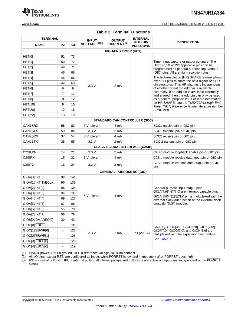
Table 2. Terminal FunctionsTERMINAL INTERNALINPUT OUTPUT PULLUP/ DESCRIPTIONVOLTAGE (1) (2) CURRENT (3)NAME PZ PGE PULLDOWN
HIGH-END TIMER (HET)HET[0] 51 73
Timer input capture or output compare. TheHET[1] 50 72HET[8:0,18,20,22] applicable pins can beHET[2] 49 71 programmed as general-purpose input/output
HET[3] 46 66 (GIO) pins. All are high-resolution pins.The high-resolution (HR) SHARE feature allowsHET[4] 45 65even HR pins to share the next higher odd HR
HET[5] 44 63 pin structures. This HR sharing is independent3.3 V 2 mAof whether or not the odd pin is availableHET[6] 6 9externally. If an odd pin is available externallyHET[7] 7 11 and shared, then the odd pin can only be used
HET[8] 8 12 as a general-purpose I/O. For more informationon HR SHARE, see the TMS470R1x High-EndHET[18] 9 15 Timer (HET) Reference Guide (literature number
HET[20] 12 18 SPNU199).HET[22] 13 19
STANDARD CAN CONTROLLER (SCC)CAN1SRX 58 83 5-V tolerant 4 mA SCC1 receive pin or GIO pinCAN1STX 59 84 3.3 V 2 mA SCC1 transmit pin or GIO pinCAN2SRX 37 54 5-V tolerant 4 mA SCC2 receive pin or GIO pinCAN2STX 38 55 3.3 V 2 mA SCC 2 transmit pin or GIO pin
CLASS II SERIAL INTERFACE (C2SIB)C2SILPN 14 21 3.3 V 2 mA C2SIb module loopback enable pin or GIO pinC2SIRX 15 22 5-V tolerant 4 mA C2SIb module receive data input pin or GIO pin
C2SIb module transmit data output pin or GIOC2SITX 16 24 3.3 V 2 mA pinGENERAL-PURPOSE I/O (GIO)
GIOA[0]/INT[0] 99 141GIOA[1]/INT[1]/ECLK 96 136GIOA[2]/INT[2] 95 134 General-purpose input/output pins.
GIOA[7:0]/INT[7:0] are interrupt-capable pins.GIOA[3]/INT[3] 94 1335-V tolerant 4 mA GIOA[1]/INT[1]/ECLK pin is multiplexed with theGIOA[4]/INT[4] 89 127 external clock-out function of the external clock
prescale (ECP) module.GIOA[5]/INT[5] 67 98GIOA[6]/INT[6] 55 78GIOA[7]/INT[7] 56 79GIOB[0]/DMAREQ[0] 30 43GIOC[0]/EBOE - 135 GIOB[0], GIOC[4:0], GIOD[5:0], GIOE[7:0:],GIOC[1]/EBWR[0] - 128 GIOF[7:0], GIOG[7:0], and GIOH[5:0] are
3.3 V 2 mA IPD (20 µA) multiplexed with the expansion bus module.GIOC[2]/EBWR[1] - 126See Table 7.GIOC[3]/EBCS[5] - 120
GIOC[4]/EBCS[6] - 119
(1) PWR = power, GND = ground, REF = reference voltage, NC = no connect(2) All I/O pins, except RST, are configured as inputs while PORRST is low and immediately after PORRST goes high.(3) IPD = internal pulldown, IPU = internal pullup (all internal pullups and pulldowns are active on input pins, independent of the PORRST
state.)
Copyright © 2005–2008, Texas Instruments Incorporated Submit Documentation Feedback 9
Product Folder Link(s): TMS470R1A384
TMS470R1A384
SPNS110E–AUGUST 2005–REVISED MAY 2008 ......................................................................................................................................................... www.ti.com
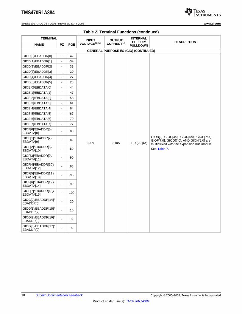
Table 2. Terminal Functions (continued)TERMINAL INTERNALINPUT OUTPUT PULLUP/ DESCRIPTIONVOLTAGE (1) (2) CURRENT (3)NAME PZ PGE PULLDOWN
GENERAL-PURPOSE I/O (GIO) (CONTINUED)GIOD[0]/EBADDR[0] - 42GIOD[1]/EBADDR[1] - 39GIOD[2]/EBADDR[2] - 35GIOD[3]/EBADDR[3] - 30GIOD[4]/EBADDR[4] - 27GIOD[5]/EBADDR[5] - 23GIOE[0]/EBDATA[0] - 44GIOE[1]/EBDATA[1] - 47GIOE[2]/EBDATA[2] - 58GIOE[3]/EBDATA[3] - 61GIOE[4]/EBDATA[4] - 64GIOE[5]/EBDATA[5] - 67GIOE[6]/EBDATA[6] - 70GIOE[7]/EBDATA[7] - 77GIOF[0]/EBADDR[6]/ - 80EBDATA[8]
GIOB[0], GIOC[4:0], GIOD[5:0], GIOE[7:0:],GIOF[1]/EBADDR[7]/ - 82 GIOF[7:0], GIOG[7:0], AND GIOH[5:0] areEBDATA[9] 3.3 V 2 mA IPD (20 µA) multiplexed with the expansion bus module.GIOF[2]/EBADDR[8]/ - 89 See Table 7.EBDATA[10]GIOF[3]/EBADDR[9]/ - 90EBDATA[11]GIOF[4]/EBADDR[10]/ - 93EBDATA[12]GIOF[5]/EBADDR[11]/ - 96EBDATA[13]GIOF[6]/EBADDR[12]/ - 99EBDATA[14]GIOF[7]/EBADDR[13]/ - 100EBDATA[15]GIOG[0]/EBADDR[14]/ - 20EBADDR[6]GIOG[1]/EBADDR[15]/ - 10EBADDR[7]GIOG[2]/EBADDR[16]/ - 8EBADDR[8]GIOG[3]/EBADDR[17]/ - 6EBADDR[9]
10 Submit Documentation Feedback Copyright © 2005–2008, Texas Instruments Incorporated
Product Folder Link(s): TMS470R1A384
TMS470R1A384
www.ti.com ......................................................................................................................................................... SPNS110E–AUGUST 2005–REVISED MAY 2008
Table 2. Terminal Functions (continued)TERMINAL INTERNALINPUT OUTPUT PULLUP/ DESCRIPTIONVOLTAGE (1) (2) CURRENT (3)NAME PZ PGE PULLDOWN
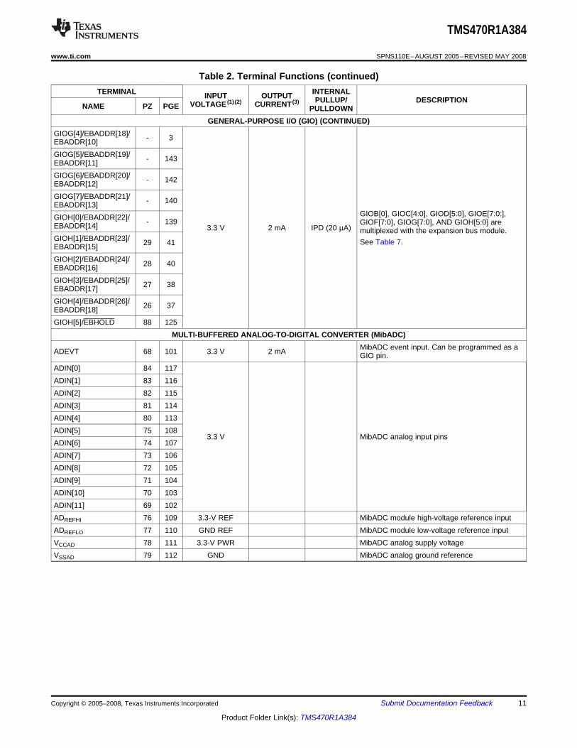
GENERAL-PURPOSE I/O (GIO) (CONTINUED)GIOG[4]/EBADDR[18]/ - 3EBADDR[10]GIOG[5]/EBADDR[19]/ - 143EBADDR[11]GIOG[6]/EBADDR[20]/ - 142EBADDR[12]GIOG[7]/EBADDR[21]/ - 140EBADDR[13]
GIOB[0], GIOC[4:0], GIOD[5:0], GIOE[7:0:],GIOH[0]/EBADDR[22]/ - 139 GIOF[7:0], GIOG[7:0], AND GIOH[5:0] areEBADDR[14] 3.3 V 2 mA IPD (20 µA) multiplexed with the expansion bus module.GIOH[1]/EBADDR[23]/ See Table 7.29 41EBADDR[15]GIOH[2]/EBADDR[24]/ 28 40EBADDR[16]GIOH[3]/EBADDR[25]/ 27 38EBADDR[17]GIOH[4]/EBADDR[26]/ 26 37EBADDR[18]GIOH[5]/EBHOLD 88 125
MULTI-BUFFERED ANALOG-TO-DIGITAL CONVERTER (MibADC)MibADC event input. Can be programmed as aADEVT 68 101 3.3 V 2 mA GIO pin.
ADIN[0] 84 117ADIN[1] 83 116ADIN[2] 82 115ADIN[3] 81 114ADIN[4] 80 113ADIN[5] 75 108
3.3 V MibADC analog input pinsADIN[6] 74 107ADIN[7] 73 106ADIN[8] 72 105ADIN[9] 71 104ADIN[10] 70 103ADIN[11] 69 102ADREFHI 76 109 3.3-V REF MibADC module high-voltage reference inputADREFLO 77 110 GND REF MibADC module low-voltage reference inputVCCAD 78 111 3.3-V PWR MibADC analog supply voltageVSSAD 79 112 GND MibADC analog ground reference
Copyright © 2005–2008, Texas Instruments Incorporated Submit Documentation Feedback 11
Product Folder Link(s): TMS470R1A384
TMS470R1A384
SPNS110E–AUGUST 2005–REVISED MAY 2008 ......................................................................................................................................................... www.ti.com
Table 2. Terminal Functions (continued)TERMINAL INTERNALINPUT OUTPUT PULLUP/ DESCRIPTIONVOLTAGE (1) (2) CURRENT (3)NAME PZ PGE PULLDOWN
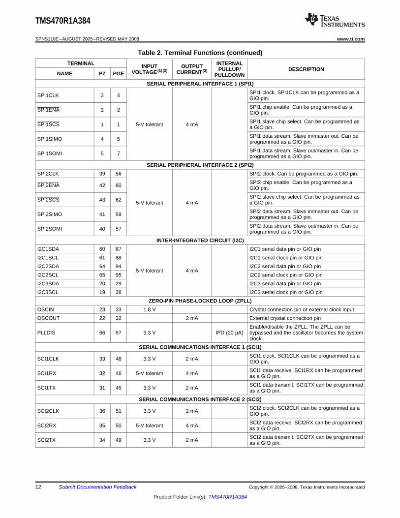
SERIAL PERIPHERAL INTERFACE 1 (SPI1)SPI1 clock. SPI1CLK can be programmed as aSPI1CLK 3 4 GIO pin.SPI1 chip enable. Can be programmed as aSPI1ENA 2 2 GIO pin.SPI1 slave chip select. Can be programmed asSPI1SCS 1 1 5-V tolerant 4 mA a GIO pin.SPI1 data stream. Slave in/master out. Can beSPI1SIMO 4 5 programmed as a GIO pin.SPI1 data stream. Slave out/master in. Can beSPI1SOMI 5 7 programmed as a GIO pin.
SERIAL PERIPHERAL INTERFACE 2 (SPI2)SPI2CLK 39 56 SPI2 clock. Can be programmed as a GIO pin.
SPI2 chip enable. Can be programmed as aSPI2ENA 42 60 GIO pin.SPI2 slave chip select. Can be programmed asSPI2SCS 43 62 5-V tolerant 4 mA a GIO pin.SPI2 data stream. Slave in/master out. Can beSPI2SIMO 41 59 programmed as a GIO pin.SPI2 data stream. Slave out/master in. Can beSPI2SOMI 40 57 programmed as a GIO pin.
INTER-INTEGRATED CIRCUIT (I2C)I2C1SDA 60 87 I2C1 serial data pin or GIO pinI2C1SCL 61 88 I2C1 serial clock pin or GIO pinI2C2SDA 64 94 I2C2 serial data pin or GIO pin
5-V tolerant 4 mAI2C2SCL 65 95 I2C2 serial clock pin or GIO pinI2C3SDA 20 29 I2C3 serial data pin or GIO pinI2C3SCL 19 28 I2C3 serial clock pin or GIO pin
ZERO-PIN PHASE-LOCKED LOOP (ZPLL)OSCIN 23 33 1.8 V Crystal connection pin or external clock inputOSCOUT 22 32 2 mA External crystal connection pin
Enable/disable the ZPLL. The ZPLL can bePLLDIS 66 97 3.3 V IPD (20 µA) bypassed and the oscillator becomes the system
clock.SERIAL COMMUNICATIONS INTERFACE 1 (SCI1)
SCI1 clock. SCI1CLK can be programmed as aSCI1CLK 33 48 3.3 V 2 mA GIO pin.SCI1 data receive. SCI1RX can be programmedSCI1RX 32 46 5-V tolerant 4 mA as a GIO pin.SCI1 data transmit. SCI1TX can be programmedSCI1TX 31 45 3.3 V 2 mA as a GIO pin.
SERIAL COMMUNICATIONS INTERFACE 2 (SCI2)SCI2 clock. SCI2CLK can be programmed as aSCI2CLK 36 51 3.3 V 2 mA GIO pin.SCI2 data receive. SCI2RX can be programmedSCI2RX 35 50 5-V tolerant 4 mA as a GIO pin.SCI2 data transmit. SCI2TX can be programmedSCI2TX 34 49 3.3 V 2 mA as a GIO pin.
12 Submit Documentation Feedback Copyright © 2005–2008, Texas Instruments Incorporated
Product Folder Link(s): TMS470R1A384
TMS470R1A384
www.ti.com ......................................................................................................................................................... SPNS110E–AUGUST 2005–REVISED MAY 2008
Table 2. Terminal Functions (continued)TERMINAL INTERNALINPUT OUTPUT PULLUP/ DESCRIPTIONVOLTAGE (1) (2) CURRENT (3)NAME PZ PGE PULLDOWN
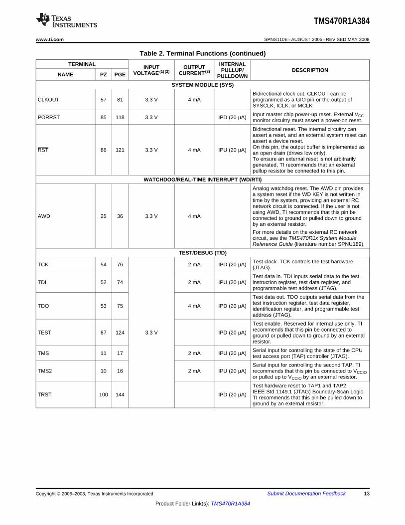
SYSTEM MODULE (SYS)Bidirectional clock out. CLKOUT can be
CLKOUT 57 81 3.3 V 4 mA programmed as a GIO pin or the output ofSYSCLK, ICLK, or MCLK.Input master chip power-up reset. External VCCPORRST 85 118 3.3 V IPD (20 µA) monitor circuitry must assert a power-on reset.Bidirectional reset. The internal circuitry canassert a reset, and an external system reset canassert a device reset.On this pin, the output buffer is implemented asRST 86 121 3.3 V 4 mA IPU (20 µA) an open drain (drives low only).To ensure an external reset is not arbitrarilygenerated, TI recommends that an externalpullup resistor be connected to this pin.
WATCHDOG/REAL-TIME INTERRUPT (WD/RTI)Analog watchdog reset. The AWD pin providesa system reset if the WD KEY is not written intime by the system, providing an external RCnetwork circuit is connected. If the user is notusing AWD, TI recommends that this pin be
AWD 25 36 3.3 V 4 mA connected to ground or pulled down to groundby an external resistor.For more details on the external RC networkcircuit, see the TMS470R1x System ModuleReference Guide (literature number SPNU189).
TEST/DEBUG (T/D)Test clock. TCK controls the test hardwareTCK 54 76 2 mA IPD (20 µA) (JTAG).Test data in. TDI inputs serial data to the test
TDI 52 74 2 mA IPU (20 µA) instruction register, test data register, andprogrammable test address (JTAG).Test data out. TDO outputs serial data from thetest instruction register, test data register,TDO 53 75 4 mA IPD (20 µA) identification register, and programmable testaddress (JTAG).Test enable. Reserved for internal use only. TIrecommends that this pin be connected toTEST 87 124 3.3 V IPD (20 µA) ground or pulled down to ground by an externalresistor.Serial input for controlling the state of the CPUTMS 11 17 2 mA IPU (20 µA) test access port (TAP) controller (JTAG).Serial input for controlling the second TAP. TI
TMS2 10 16 2 mA IPU (20 µA) recommends that this pin be connected to VCCIOor pulled up to VCCIO by an external resistor.Test hardware reset to TAP1 and TAP2.IEEE Std 1149.1 (JTAG) Boundary-Scan Logic.TRST 100 144 IPD (20 µA) TI recommends that this pin be pulled down toground by an external resistor.
Copyright © 2005–2008, Texas Instruments Incorporated Submit Documentation Feedback 13
Product Folder Link(s): TMS470R1A384
TMS470R1A384
SPNS110E–AUGUST 2005–REVISED MAY 2008 ......................................................................................................................................................... www.ti.com
Table 2. Terminal Functions (continued)TERMINAL INTERNALINPUT OUTPUT PULLUP/ DESCRIPTIONVOLTAGE (1) (2) CURRENT (3)NAME PZ PGE PULLDOWN
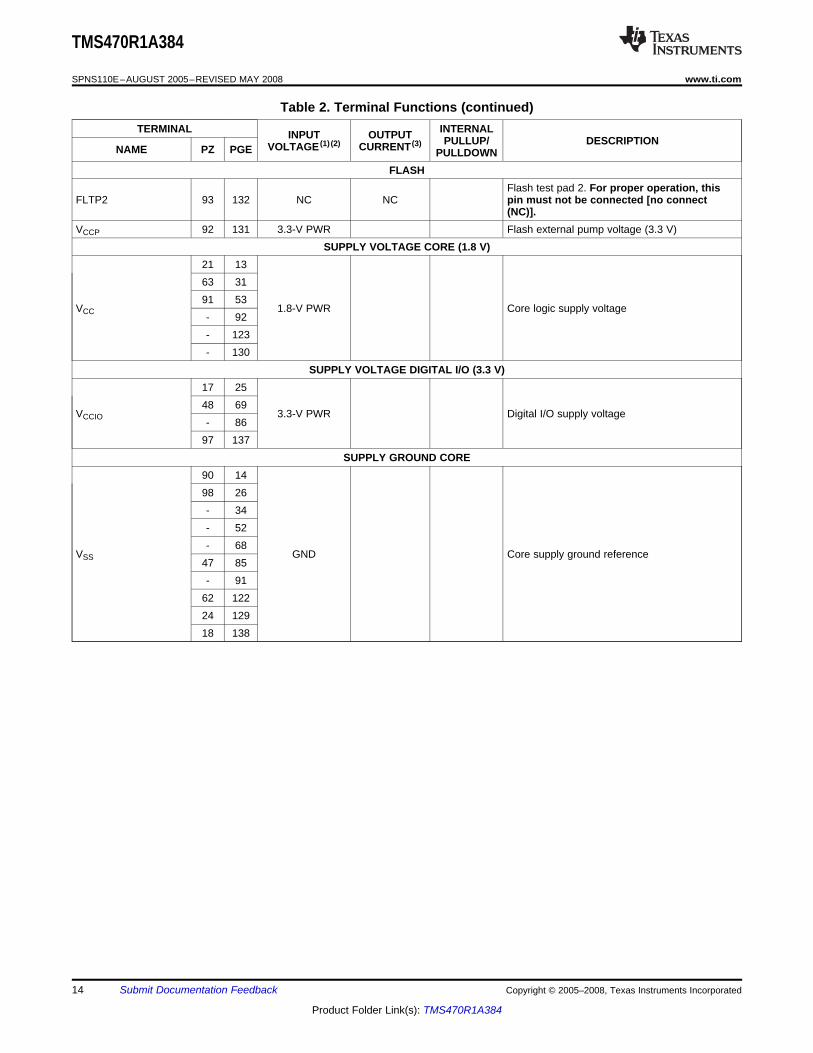
FLASHFlash test pad 2. For proper operation, this
FLTP2 93 132 NC NC pin must not be connected [no connect(NC)].
VCCP 92 131 3.3-V PWR Flash external pump voltage (3.3 V)SUPPLY VOLTAGE CORE (1.8 V)
21 1363 3191 53
VCC 1.8-V PWR Core logic supply voltage- 92- 123- 130
SUPPLY VOLTAGE DIGITAL I/O (3.3 V)17 2548 69
VCCIO 3.3-V PWR Digital I/O supply voltage- 86
97 137SUPPLY GROUND CORE
90 1498 26- 34- 52- 68
VSS GND Core supply ground reference47 85- 91
62 12224 12918 138
14 Submit Documentation Feedback Copyright © 2005–2008, Texas Instruments Incorporated
Product Folder Link(s): TMS470R1A384
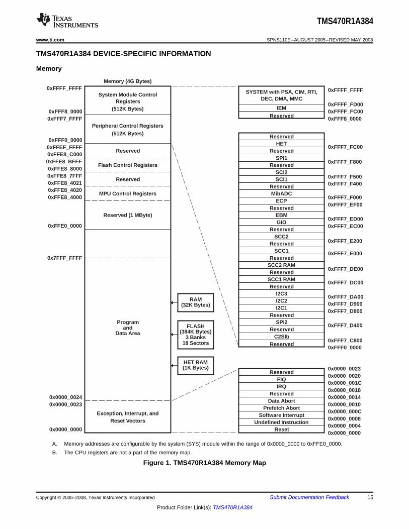
TMS470R1A384 DEVICE-SPECIFIC INFORMATION
Memory
System Module Control
(512K Bytes)
(512K Bytes)Peripheral Control Registers
Reserved
Flash Control Registers
Reserved
MPU Control Registers
Reserved (1 MByte)
Programand
Data Area
Exception, Interrupt, andReset Vectors
SYSTEM with PSA, CIM, RTI,DEC, DMA, MMC
IEMReserved
ReservedHET
ReservedSPI1
ReservedSCI2SCI1
ReservedMibADC
ECPReserved
EBMGIO
ReservedSCC2
ReservedSCC1
ReservedSCC2 RAMReserved
SCC1 RAMReserved
I2C3I2C2I2C1
ReservedSPI2
ReservedC2SIb
Reserved
ReservedFIQIRQ
ReservedData Abort
Prefetch AbortSoftware Interrupt
Undefined InstructionReset
RAM(32K Bytes)
FLASH(384K Bytes)
3 Banks
Memory (4G Bytes)0xFFFF_FFFF
0xFFF8_00000xFFF7_FFFF
0xFFF0_00000xFFEF_FFFF0xFFE8_C0000xFFE8_BFFF0xFFE8_80000xFFE8_7FFF0xFFE8_40210xFFE8_40200xFFE8_4000
0xFFE0_0000
0x7FFF_FFFF
0x0000_00240x0000_0023
0x0000_0000
0xFFFF_FFFF
0xFFFF_FD000xFFFF_FC000xFFF8_0000
0xFFF7_FC00
0xFFF7_F800
0xFFF7_F5000xFFF7_F400
0xFFF7_F0000xFFF7_EF00
0xFFF7_ED000xFFF7_EC00
0xFFF7_E200
0xFFF7_E000
0xFFF7_DE00
0xFFF7_DC00
0xFFF7_DA00
0xFFF7_D800
0xFFF7_D400
0xFFF7_C8000xFFF0_0000
0x0000_00230x0000_00200x0000_001C0x0000_00180x0000_00140x0000_00100x0000_000C0x0000_00080x0000_00040x0000_0000
Registers
0xFFF7_D900
18 Sectors
HET RAM(1K Bytes)
TMS470R1A384
www.ti.com ......................................................................................................................................................... SPNS110E–AUGUST 2005–REVISED MAY 2008
A. Memory addresses are configurable by the system (SYS) module within the range of 0x0000_0000 to 0xFFE0_0000.B. The CPU registers are not a part of the memory map.
Figure 1. TMS470R1A384 Memory Map
Copyright © 2005–2008, Texas Instruments Incorporated Submit Documentation Feedback 15
Product Folder Link(s): TMS470R1A384
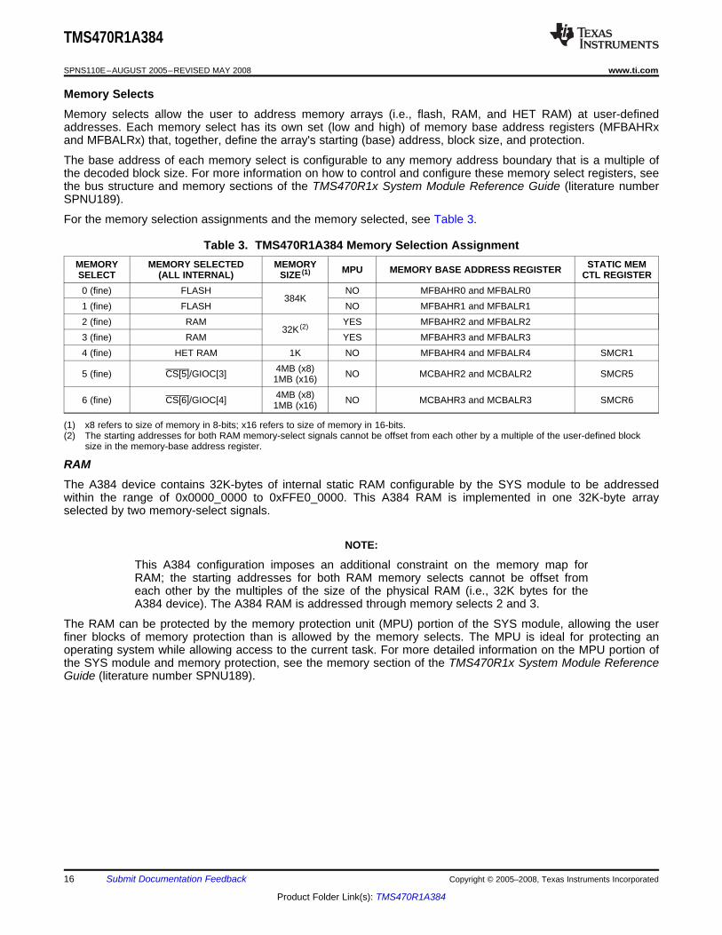
Memory Selects
TMS470R1A384
SPNS110E–AUGUST 2005–REVISED MAY 2008 ......................................................................................................................................................... www.ti.com
Memory selects allow the user to address memory arrays (i.e., flash, RAM, and HET RAM) at user-definedaddresses. Each memory select has its own set (low and high) of memory base address registers (MFBAHRxand MFBALRx) that, together, define the array's starting (base) address, block size, and protection.
The base address of each memory select is configurable to any memory address boundary that is a multiple ofthe decoded block size. For more information on how to control and configure these memory select registers, seethe bus structure and memory sections of the TMS470R1x System Module Reference Guide (literature numberSPNU189).
For the memory selection assignments and the memory selected, see Table 3.
Table 3. TMS470R1A384 Memory Selection AssignmentMEMORY MEMORY SELECTED MEMORY STATIC MEMMPU MEMORY BASE ADDRESS REGISTERSELECT (ALL INTERNAL) SIZE (1) CTL REGISTER
0 (fine) FLASH NO MFBAHR0 and MFBALR0384K
1 (fine) FLASH NO MFBAHR1 and MFBALR12 (fine) RAM YES MFBAHR2 and MFBALR2
32K (2)3 (fine) RAM YES MFBAHR3 and MFBALR34 (fine) HET RAM 1K NO MFBAHR4 and MFBALR4 SMCR1
4MB (x8)5 (fine) CS[5]/GIOC[3] NO MCBAHR2 and MCBALR2 SMCR51MB (x16)4MB (x8)6 (fine) CS[6]/GIOC[4] NO MCBAHR3 and MCBALR3 SMCR61MB (x16)
(1) x8 refers to size of memory in 8-bits; x16 refers to size of memory in 16-bits.(2) The starting addresses for both RAM memory-select signals cannot be offset from each other by a multiple of the user-defined block
size in the memory-base address register.
RAMThe A384 device contains 32K-bytes of internal static RAM configurable by the SYS module to be addressedwithin the range of 0x0000_0000 to 0xFFE0_0000. This A384 RAM is implemented in one 32K-byte arrayselected by two memory-select signals.
NOTE:
This A384 configuration imposes an additional constraint on the memory map forRAM; the starting addresses for both RAM memory selects cannot be offset fromeach other by the multiples of the size of the physical RAM (i.e., 32K bytes for theA384 device). The A384 RAM is addressed through memory selects 2 and 3.
The RAM can be protected by the memory protection unit (MPU) portion of the SYS module, allowing the userfiner blocks of memory protection than is allowed by the memory selects. The MPU is ideal for protecting anoperating system while allowing access to the current task. For more detailed information on the MPU portion ofthe SYS module and memory protection, see the memory section of the TMS470R1x System Module ReferenceGuide (literature number SPNU189).
16 Submit Documentation Feedback Copyright © 2005–2008, Texas Instruments Incorporated
Product Folder Link(s): TMS470R1A384
TMS470R1A384
www.ti.com ......................................................................................................................................................... SPNS110E–AUGUST 2005–REVISED MAY 2008
F05 FlashThe F05 flash memory is a nonvolatile electrically erasable and programmable memory implemented with a32-bit-wide data bus interface. The F05 flash has an external state machine for programming and erasefunctions. See the Flash Read and Flash Program and Erase sections.
Flash Protection Keys
The A384 device provides flash protection keys. These four 32-bit protection keys preventprogram/erase/compaction operations from occurring until after the four protection keys have been matched bythe CPU loading the correct user keys into the FMPKEY control register. The protection keys on the A384 arelocated in the last 4 words of the first 8K sector. For more detailed information on the flash protection keys andthe FMPKEY control register, see the "Optional Quadruple Protection Keys" and "Programming the ProtectionKeys" portions of the TMS470R1x F05 Flash Reference Guide (literature number SPNU213).
Flash Read
The A384 flash memory is configurable by the SYS module to be addressed within the range of 0x0000_0000 to0xFFE0_0000. The flash is addressed through memory selects 0 and 1.
NOTE:
The flash external pump voltage (VCCP) is required for all operations (program, erase,and read).
Flash Pipeline Mode
When in pipeline mode, the flash operates with a system clock frequency of up to 48 MHz (versus a systemclock frequency of 24 MHz in normal mode). Flash in pipeline mode is capable of accessing 64-bit words andprovides two 32-bit pipelined words to the CPU. Also, in pipeline mode the flash can be read with no wait stateswhen memory addresses are contiguous (after the initial 1- or 2-wait-state reads).
NOTE:
After a system reset, pipeline mode is disabled (FMREGOPT[0] = 0). In other words,the A384 device powers up and comes out of reset in non-pipeline mode.Furthermore, setting the flash configuration mode bit (GBLCTRL[4]) overrides pipelinemode.
Copyright © 2005–2008, Texas Instruments Incorporated Submit Documentation Feedback 17
Product Folder Link(s): TMS470R1A384
Peripheral Selects and Base Addresses
TMS470R1A384
SPNS110E–AUGUST 2005–REVISED MAY 2008 ......................................................................................................................................................... www.ti.com
Flash Program and Erase
The A384 device flash contains three 128K-byte memory arrays (or banks), for a total of 384K-bytes of flash, andconsists of 18 sectors. These 18 sectors are sized as follows:
SECTOR MEMORY ARRAYSSEGMENT LOW ADDRESS HIGH ADDRESSNO. (OR BANKS)0 8K Bytes 0x0000_0000 0x0000_1FFF1 8K Bytes 0x0000_2000 0x0000_3FFF2 16K Bytes 0x0000_4000 0x0000_7FFF3 16K Bytes 0x0000_8000 0x0000_BFFF4 16K Bytes 0x0000_C000 0x0000_FFFF BANK0
(128K Bytes)5 16K Bytes 0x0001_0000 0x0001_3FFF6 16K Bytes 0x0001_4000 0x0001_7FFF7 16K Bytes 0x0001_8000 0x0001_BFFF8 8K Bytes 0x0001_C000 0x0001_DFFF9 8K bytes 0x0001_E000 0x0001_FFFF
0 32K Bytes 0x0002_0000 0x0002_7FFF1 32K Bytes 0x0002_8000 0x0002_FFFF BANK1
(128K Bytes)2 32K Bytes 0x0003_0000 0x0003_7FFF3 32K Bytes 0x0003_8000 0x0003_FFFF
0 32K Bytes 0x0004_0000 0x0004_7FFF1 32K Bytes 0x0004_8000 0x0004_FFFF BANK2
(128K Bytes)2 32K Bytes 0x0005_0000 0x0005_7FFF3 32K Bytes 0x0005_8000 0x0005_FFFF
The minimum size for an erase operation is one sector. The maximum size for a program operation is one 16-bitword.
NOTE:
The flash external pump voltage (VCCP) is required for all operations (program, erase,and read).
Execution can occur from one bank while programming/erasing any or all sectors of another bank. However,execution cannot occur from any sector within a bank that is being programmed or erased.
NOTE:
When the OTP sector is enabled, the rest of the flash memory is disabled. The OTPmemory can only be read or programmed from code executed out of RAM.
For more detailed information on flash program and erase operations, see the TMS470R1x F05 Flash ReferenceGuide (literature number SPNU213).
HET RAMThe A384 device contains HET RAM. The HET RAM has a 64-instruction capability. The HET RAM isconfigurable by the SYS module to be addressed within the range of 0x0000_0000 to 0xFFE0_0000. The HETRAM is addressed through memory select 4.
The A384 device uses 10 of the 16 peripheral selects to decode the base addresses of the peripherals. Theseperipheral selects are fixed and transparent to the user because they are part of the decoding scheme used bythe SYS module.
Control registers for the peripherals, SYS module, and flash begin at the base addresses shown in Table 4.
18 Submit Documentation Feedback Copyright © 2005–2008, Texas Instruments Incorporated
Product Folder Link(s): TMS470R1A384
TMS470R1A384
www.ti.com ......................................................................................................................................................... SPNS110E–AUGUST 2005–REVISED MAY 2008
Table 4. A384 Peripherals, System Module, and Flash Base AddressesADDRESS RANGE
CONNECTING MODULE PERIPHERAL SELECTSBASE ADDRESS ENDING ADDRESS
SYSTEM 0xFFFF_FFCC 0x FFFF_FFFF N/AReserved 0xFFFF_FF60 0xFFFF_FFCB N/A
PSA 0xFFFF_FF40 0xFFFF_FF5F N/ACIM 0xFFFF_FF20 0xFFFF_FF3F N/ARTI 0xFFFF_FF00 0xFFFF_FF1F N/A
DMA 0xFFFF_FE80 0xFFFF_FEFF N/ADEC 0xFFFF_FE00 0xFFFF_FE7F N/AMMC 0xFFFF_FD00 0xFFFF_FD7F N/AIEM 0xFFFF_FC00 0xFFFF_FCFF N/A
Reserved 0xFFFF_FB00 0xFFFF_FBFF N/AReserved 0xFFFF_FA00 0xFFFF_FAFF N/A
DMA CMD BUFFER 0xFFFF_F800 0xFFFF_F9FF N/AReserved 0xFFF8_0000 0xFFFF_F7FF N/A
HET 0xFFF7_FC00 0xFFF7_FFFF PS[0]SPI1 0xFFF7_F800 0xFFF7_FBFF PS[1]SCI2 0XFFF7_F500 0XFFF7_F7FF
PS[2]SCI1 0xFFF7_F400 0xFFF7_F4FF
MibADC 0xFFF7_F000 0xFFF7_F3FF PS[3]ECP 0xFFF7_EF00 0xFFF7_EFFF
Reserved 0xFFF7_EE00 0xFFF7_EEFFPS[4]
EBM 0xFFF7_ED00 0xFFF7_EDFFGIO 0xFFF7_EC00 0xFFF7_ECFF
Reserved 0xFFF7_E400 0xFFF7_EBFF PS[5]–PS[6]Reserved 0xFFF7_E300 0xFFF7_E3FF
SCC2 0xFFF7_E200 0xFFF7_E2FFPS[7]
Reserved 0xFFF7_E100 0xFFF7_E1FFSCC1 0xFFF7_E000 0xFFF7_E0FF
Reserved 0xFFF7_DF00 0xFFF7_DFFFSCC2 RAM 0xFFF7_DE00 0xFFF7_DEFF
PS[8]Reserved 0xFFF7_DD00 0xFFF7_DDFF
SCC1 RAM 0xFFF7_DC00 0xFFF7_DCFFReserved 0xFFF7_DB00 0xFFF7_DBFF
I2C3 0xFFF7_DA00 0xFFF7_DAFFPS[9]
I2C2 0xFFF7_D900 0xFFF7_D9FFI2C1 0xFFF7_D800 0xFFF7_D8FFSPI2 0xFFF7_D400 0xFFF7_D7FF PS[10]
Reserved 0xFFF7_CC00 0xFFF7_D3FF PS[11]–PS[12]C2SIb 0xFFF7_C800 0xFFF7_CBFF PS[13]
Reserved 0xFFF7_C000 0xFFF7_C7FF PS[14]–PS[15]Reserved 0xFFF0_0000 0xFFF7_BFFF N/A
Flash Control Registers 0xFFE8_8000 0xFFE8_BFFF N/AMPU Control Registers 0xFFE8_4000 0xFFE8_4023 N/A
Copyright © 2005–2008, Texas Instruments Incorporated Submit Documentation Feedback 19
Product Folder Link(s): TMS470R1A384
Direct Memory Access (DMA)
TMS470R1A384
SPNS110E–AUGUST 2005–REVISED MAY 2008 ......................................................................................................................................................... www.ti.com
The DMA controller transfers data to and from any specified location in the A384 memory map (except forrestricted memory locations like the system control registers area). The DMA manages up to 16 channels, andsupports data transfer for both on-chip and off-chip memories and peripherals. The DMA controller is connectedto both the CPU and peripheral buses, enabling these data transfers to occur in parallel with CPU activity and,thus, maximizing overall system performance.
Although the DMA controller has two possible configurations for the A384 device, the DMA controllerconfiguration is 32 control packets and 16 channels.
For the A384 DMA request hardwired configuration, see Table 5.
Table 5. DMA Request Lines Connections (1)
MODULES DMA REQUEST INTERRUPT SOURCES DMA CHANNELEBM Expansion bus DMA request EBDMAREQ0 DMAREQ[0]SPI1 SPI1 end-receive SPI1DMA0 DMAREQ[1]SPI1 SPI1 end-transmit SPI1DMA1 DMAREQ[2]I2C1 I2C1 read I2C1DMA0 DMAREQ[3]SCI1 SCI1 end-receive SCI1DMA0 DMAREQ[4]SCI1 SCI1 end-transmit SCI1DMA1 DMAREQ[5]I2C1 I2C1 write I2C1DMA1 DMAREQ[6]SPI2 SPI2 end-receive SPI2DMA0 DMAREQ[7]SPI2 SPI2 end-transmit SPI2DMA1 DMAREQ[8]
I2C2/C2SIb I2C2 read/C2SIb end-receive I2C2DMA0/C2SIDMA0 DMAREQ[9]I2C2/C2SIb I2C2 write/C2SIb end-transmit I2C2DMA1/C2SIDMA1 DMAREQ[10]
I2C3 I2C3 read I2C3DMA0 DMAREQ[11]I2C3 I2C3 write I2C3DMA1 DMAREQ[12]
Reserved DMAREQ[13]SCI2/SPI3 SCI2 end-receive SCI2DMA0 DMAREQ[14]SCI2/SPI3 SCI2 end-transmit SCI2DMA1 DMAREQ[15]
(1) For DMA channels with more than one assigned request source (I2C2/C2SIb), only one of the sources listed can be the DMA requestgenerator in a given application. The device has software control to ensure that there are no conflicts between requesting modules.
Each channel has two control packets attached to it, allowing the DMA to continuously load RAM and generateperiodic interrupts so that the data can be read by the CPU. The control packets allow for the interrupt enable,and the channels determine the priority level of the interrupt.
DMA transfers occur in one of two modes:• Non-request mode (used when transferring from memory to memory)• Request mode (used when transferring from memory to peripheral)
For more detailed functional information on the DMA controller, see the TMS470R1x Direct Memory Access(DMA) Controller Reference Guide (literature number SPNU194).
20 Submit Documentation Feedback Copyright © 2005–2008, Texas Instruments Incorporated
Product Folder Link(s): TMS470R1A384
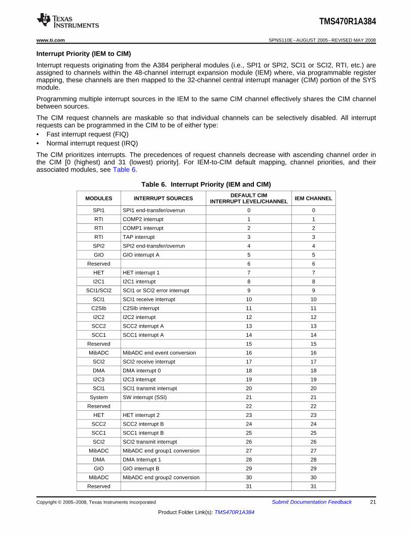
Interrupt Priority (IEM to CIM)
TMS470R1A384
www.ti.com ......................................................................................................................................................... SPNS110E–AUGUST 2005–REVISED MAY 2008
Interrupt requests originating from the A384 peripheral modules (i.e., SPI1 or SPI2, SCI1 or SCI2, RTI, etc.) areassigned to channels within the 48-channel interrupt expansion module (IEM) where, via programmable registermapping, these channels are then mapped to the 32-channel central interrupt manager (CIM) portion of the SYSmodule.
Programming multiple interrupt sources in the IEM to the same CIM channel effectively shares the CIM channelbetween sources.
The CIM request channels are maskable so that individual channels can be selectively disabled. All interruptrequests can be programmed in the CIM to be of either type:• Fast interrupt request (FIQ)• Normal interrupt request (IRQ)
The CIM prioritizes interrupts. The precedences of request channels decrease with ascending channel order inthe CIM [0 (highest) and 31 (lowest) priority]. For IEM-to-CIM default mapping, channel priorities, and theirassociated modules, see Table 6.
Table 6. Interrupt Priority (IEM and CIM)DEFAULT CIMMODULES INTERRUPT SOURCES IEM CHANNELINTERRUPT LEVEL/CHANNEL
SPI1 SPI1 end-transfer/overrun 0 0RTI COMP2 interrupt 1 1RTI COMP1 interrupt 2 2RTI TAP interrupt 3 3SPI2 SPI2 end-transfer/overrun 4 4GIO GIO interrupt A 5 5
Reserved 6 6HET HET interrupt 1 7 7I2C1 I2C1 interrupt 8 8
SCI1/SCI2 SCI1 or SCI2 error interrupt 9 9SCI1 SCI1 receive interrupt 10 10C2SIb C2SIb interrupt 11 11I2C2 I2C2 interrupt 12 12SCC2 SCC2 interrupt A 13 13SCC1 SCC1 interrupt A 14 14
Reserved 15 15MibADC MibADC end event conversion 16 16
SCI2 SCI2 receive interrupt 17 17DMA DMA interrupt 0 18 18I2C3 I2C3 interrupt 19 19SCI1 SCI1 transmit interrupt 20 20
System SW interrupt (SSI) 21 21Reserved 22 22
HET HET interrupt 2 23 23SCC2 SCC2 interrupt B 24 24SCC1 SCC1 interrupt B 25 25SCI2 SCI2 transmit interrupt 26 26
MibADC MibADC end group1 conversion 27 27DMA DMA Interrupt 1 28 28GIO GIO interrupt B 29 29
MibADC MibADC end group2 conversion 30 30Reserved 31 31
Copyright © 2005–2008, Texas Instruments Incorporated Submit Documentation Feedback 21
Product Folder Link(s): TMS470R1A384
TMS470R1A384
SPNS110E–AUGUST 2005–REVISED MAY 2008 ......................................................................................................................................................... www.ti.com
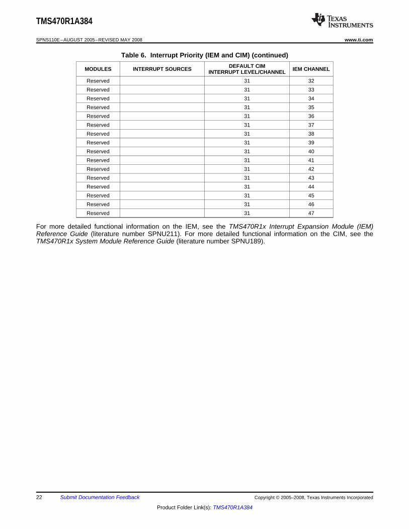
Table 6. Interrupt Priority (IEM and CIM) (continued)DEFAULT CIMMODULES INTERRUPT SOURCES IEM CHANNELINTERRUPT LEVEL/CHANNEL
Reserved 31 32Reserved 31 33Reserved 31 34Reserved 31 35Reserved 31 36Reserved 31 37Reserved 31 38Reserved 31 39Reserved 31 40Reserved 31 41Reserved 31 42Reserved 31 43Reserved 31 44Reserved 31 45Reserved 31 46Reserved 31 47
For more detailed functional information on the IEM, see the TMS470R1x Interrupt Expansion Module (IEM)Reference Guide (literature number SPNU211). For more detailed functional information on the CIM, see theTMS470R1x System Module Reference Guide (literature number SPNU189).
22 Submit Documentation Feedback Copyright © 2005–2008, Texas Instruments Incorporated
Product Folder Link(s): TMS470R1A384
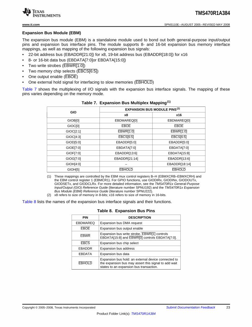
Expansion Bus Module (EBM)
TMS470R1A384
www.ti.com ......................................................................................................................................................... SPNS110E–AUGUST 2005–REVISED MAY 2008
The expansion bus module (EBM) is a standalone module used to bond out both general-purpose input/outputpins and expansion bus interface pins. The module supports 8- and 16-bit expansion bus memory interfacemappings, as well as mapping of the following expansion bus signals:• 22-bit address bus (EBADDR[21:0]) for x8, 19-bit address bus (EBADDR[18:0]) for x16• 8- or 16-bit data bus (EBDATA[7:0]or EBDATA[15:0])• Two write strobes (EBWR[1:0])• Two memory chip selects (EBCS[6:5])• One output enable (EBOE)• One external hold signal for interfacing to slow memories (EBHOLD)
Table 7 shows the multiplexing of I/O signals with the expansion bus interface signals. The mapping of thesepins varies depending on the memory mode.
Table 7. Expansion Bus Multiplex Mapping (1)
EXPANSION BUS MODULE PINS (2)GIO
x8 x16GIOB[0] EBDMAREQ[0] EBDMAREQ[0]GIOC[0] EBOE EBOE
GIOC[2:1] EBWR[1:0] EBWR[1:0]GIOC[4:3] EBCS[6:5] EBCS[6:5]GIOD[5:0] EBADDR[5:0] EBADDR[5:0]GIOE[7:0] EBDATA[7:0] EBDATA[7:0]GIOF[7:0] EBADDR[13:6] EBDATA[15:8]GIOG[7:0] EBADDR[21:14] EBADDR[13:6]GIOH[4:0] – EBADDR[18:14]GIOH[5] EBHOLD EBHOLD
(1) These mappings are controlled by the EBM mux control registers B–H (EBMXCRB–EBMXCRH) andthe EBM control register 1 (EBMCR1). For GPIO functions, use GIODIRx, GIODINx, GIODOUTx,GIODSETx, and GIODCLRx. For more detailed information, see the TMS470R1x General-PurposeInput/Output (GIO) Reference Guide (literature number SPNU192) and the TMS470R1x ExpansionBus Module (EBM) Reference Guide (literature number SPNU222).
(2) x8 refers to size of memory in 8-bits; x16 refers to size of memory in 16-bits.
Table 8 lists the names of the expansion bus interface signals and their functions.
Table 8. Expansion Bus PinsPIN DESCRIPTION
EBDMAREQ Expansion bus DMA requestEBOE Expansion bus output enable
Expansion bus write strobe. EBWR[1] controlsEBWR EBDATA[15:8] and EBWR[0] controls EBDATA[7:0].EBCS Expansion bus chip select
EBADDR Expansion bus addressEBDATA Expansion bus data
Expansion bus hold: an external device connected toEBHOLD the expansion bus may assert this signal to add wait
states to an expansion bus transaction.
Copyright © 2005–2008, Texas Instruments Incorporated Submit Documentation Feedback 23
Product Folder Link(s): TMS470R1A384
MibADC
TMS470R1A384
SPNS110E–AUGUST 2005–REVISED MAY 2008 ......................................................................................................................................................... www.ti.com
The multi-buffered analog-to-digital converter (MibADC) accepts an analog signal and converts the signal to a10-bit digital value.
The A384 MibADC module can function in two modes: compatibility mode, where its programmer's model iscompatible with the TMS470R1x ADC module and its digital results are stored in digital result registers; or inbuffered mode, where the digital result registers are replaced with three FIFO buffers, one for each conversiongroup [event, group1 (G1), and group2 (G2)]. In buffered mode, the MibADC buffers can be serviced byinterrupts or by the DMA.
NOTE:
The MibADC on this device does not support the DMA.
MibADC Event Trigger EnhancementsThe MibADC includes two major enhancements over the event-triggering capability of the TMS470R1x ADC.• Both group1 and the event group can be configured for event-triggered operation, providing up to two
event-triggered groups.• The trigger source and polarity can be selected individually for both group1 and the event group from the
options identified in Table 9.
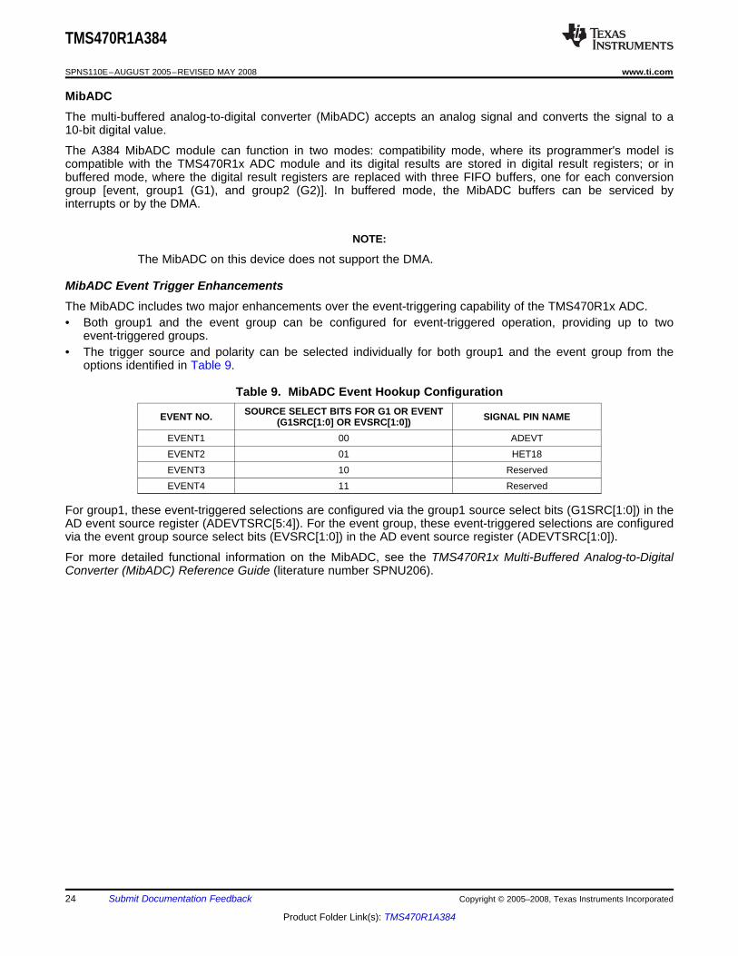
Table 9. MibADC Event Hookup ConfigurationSOURCE SELECT BITS FOR G1 OR EVENTEVENT NO. SIGNAL PIN NAME(G1SRC[1:0] OR EVSRC[1:0])
EVENT1 00 ADEVTEVENT2 01 HET18EVENT3 10 ReservedEVENT4 11 Reserved
For group1, these event-triggered selections are configured via the group1 source select bits (G1SRC[1:0]) in theAD event source register (ADEVTSRC[5:4]). For the event group, these event-triggered selections are configuredvia the event group source select bits (EVSRC[1:0]) in the AD event source register (ADEVTSRC[1:0]).
For more detailed functional information on the MibADC, see the TMS470R1x Multi-Buffered Analog-to-DigitalConverter (MibADC) Reference Guide (literature number SPNU206).
24 Submit Documentation Feedback Copyright © 2005–2008, Texas Instruments Incorporated
Product Folder Link(s): TMS470R1A384
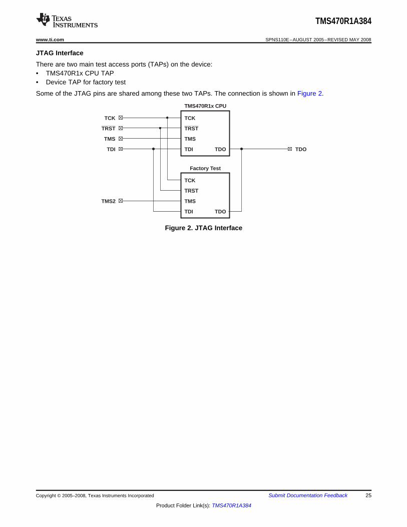
JTAG Interface
TCK
TRST
TMS
TDI TDO
TMS470R1x CPU
Factory Test
TDI
TRST
TMS
TCK
TDO
TCK
TRST
TMS
TDI
TMS2
TDO
TMS470R1A384
www.ti.com ......................................................................................................................................................... SPNS110E–AUGUST 2005–REVISED MAY 2008
There are two main test access ports (TAPs) on the device:• TMS470R1x CPU TAP• Device TAP for factory test
Some of the JTAG pins are shared among these two TAPs. The connection is shown in Figure 2.
Figure 2. JTAG Interface
Copyright © 2005–2008, Texas Instruments Incorporated Submit Documentation Feedback 25
Product Folder Link(s): TMS470R1A384
Documentation Support
TMS470R1A384
SPNS110E–AUGUST 2005–REVISED MAY 2008 ......................................................................................................................................................... www.ti.com
Extensive documentation supports all of the TMS470 microcontroller family generation of devices. The types ofdocumentation available include data sheets with design specifications, complete user's guides for all devicesand development support tools, and hardware and software applications. Useful reference documentationincludes:• Bulletin
– TMS470 Microcontroller Family Product Bulletin (literature number SPNB086)• User's Guides
– TMS470R1x System Module Reference Guide (literature number SPNU189)– TMS470R1x General Purpose Input/Output (GIO) Reference Guide (literature number SPNU192)– TMS470R1x Direct Memory Access (DMA) Controller Reference Guide (literature number SPNU194)– TMS470R1x Serial Peripheral Interface (SPI) Reference Guide (literature number SPNU195)– TMS470R1x Serial Communication Interface (SCI) Reference Guide (literature number SPNU196)– TMS470R1x Controller Area Network (CAN) Reference Guide (literature number SPNU197)– TMS470R1x High End Timer (HET) Reference Guide (literature number SPNU199)– TMS470R1x External Clock Prescale (ECP) Reference Guide (literature number SPNU202)– TMS470R1x MultiBuffered Analog to Digital (MibADC) Reference Guide (literature number SPNU206)– TMS470R1x Zero Pin Phase-Locked Loop (ZPLL) Clock Module Reference Guide (literature number
SPNU212)– TMS470R1x F05 Flash Reference Guide (literature number SPNU213)– TMS470R1x Class II Serial Interface B (C2SIb) Reference Guide (literature number SPNU214)– TMS470R1x Class II Serial Interface A (C2SIa) Reference Guide (literature number SPNU218)– TMS470R1x JTAG Security Module (JSM) Reference Guide (literature number SPNU245)– TMS470R1x Memory Security Module (MSM) Reference Guide (literature number SPNU246)– TMS470 Peripherals Overview Reference Guide (literature number SPNU248)
• Errata Sheet– TMS470R1A384 TMS470 Microcontrollers Silicon Errata (literature number SPNZ148)
26 Submit Documentation Feedback Copyright © 2005–2008, Texas Instruments Incorporated
Product Folder Link(s): TMS470R1A384

Device and Development-Support Tool Nomenclature
TMS470R1A384
www.ti.com ......................................................................................................................................................... SPNS110E–AUGUST 2005–REVISED MAY 2008
To designate the stages in the product development cycle, TI assigns prefixes to the part numbers of all DSPdevices and support tools. Each DSP commercial family member has one of three prefixes: TMX, TMP, or TMS(e.g., TMS470R1A384). Texas Instruments recommends two of three possible prefix designators for its supporttools: TMDX and TMDS. These prefixes represent evolutionary stages of product development from engineeringprototypes (TMX/TMDX) through fully qualified production devices/tools (TMS/TMDS).
Device development evolutionary flow:
TMX Experimental device that is not necessarily representative of the final device's electrical specifications
TMP Final silicon die that conforms to the device's electrical specifications but has not completed quality andreliability verification
TMS Fully qualified production device
Support tool development evolutionary flow:
TMDX Development-support product that has not yet completed Texas Instruments internal qualification testing.
TMDS Fully qualified development-support product
TMX and TMP devices and TMDX development-support tools are shipped against the following disclaimer:
"Developmental product is intended for internal evaluation purposes."
TMS devices and TMDS development-support tools have been characterized fully, and the quality and reliabilityof the device have been demonstrated fully. TI's standard warranty applies.
Predictions show that prototype devices (TMX or TMP) have a greater failure rate than the standard productiondevices. Texas Instruments recommends that these devices not be used in any production system because theirexpected end-use failure rate still is undefined. Only qualified production devices are to be used.
Figure 3 illustrates the numbering and symbol nomenclature for the TMS470R1x family.
Copyright © 2005–2008, Texas Instruments Incorporated Submit Documentation Feedback 27
Product Folder Link(s): TMS470R1A384
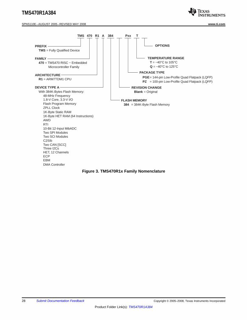
TMS 470 R1 A 384 Pxx
PREFIXTMS
FAMILY470
ARCHITECTURER1
DEVICE TYPE A
= Fully Qualified Device
= TMS470 RISC − Embedded Microcontroller Family
= ARM7TDM1 CPU
1.8-V Core, 3.3-V I/OFlash Program MemoryZPLL Clock1K-Byte Static RAM1K-Byte HET RAM (64 Instructions)AWDRTI10-Bit 12-Input MibADCTwo SPI ModulesTwo SCI ModulesC2SIbTwo CAN [SCC]
HET, 12 ChannelsECPEBM
With 384K-Bytes Flash Memory:
TEMPERATURE RANGE T = −40°C to 105°C
Q = −40°C to 125°C
PACKAGE TYPE
PGEPZ
= 144-pin Low-Profile Quad Flatpack (LQFP)= 100-pin Low-Profile Quad Flatpack (LQFP)
REVISION CHANGE Blank = Original
FLASH MEMORY 384 = 384K-Byte Flash Memory
OPTIONS
T
Three I2Cs
DMA Controller
48-MHz Frequency
TMS470R1A384
SPNS110E–AUGUST 2005–REVISED MAY 2008 ......................................................................................................................................................... www.ti.com
Figure 3. TMS470R1x Family Nomenclature
28 Submit Documentation Feedback Copyright © 2005–2008, Texas Instruments Incorporated
Product Folder Link(s): TMS470R1A384
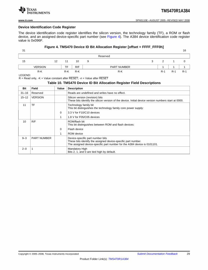
Device Identification Code Register
TMS470R1A384
www.ti.com ......................................................................................................................................................... SPNS110E–AUGUST 2005–REVISED MAY 2008
The device identification code register identifies the silicon version, the technology family (TF), a ROM or flashdevice, and an assigned device-specific part number (see Figure 4). The A384 device identification code registervalue is 0x096F.
Figure 4. TMS470 Device ID Bit Allocation Register [offset = FFFF_FFF0h]31 16
Reserved
15 12 11 10 9 3 2 1 0
VERSION TF R/F PART NUMBER 1 1 1R-K R-K R-K R-K R-1 R-1 R-1
LEGEND:R = Read only, -K = Value constant after RESET; -n = Value after RESET
Table 10. TMS470 Device ID Bit Allocation Register Field DescriptionsBit Field Value Description
31–16 Reserved Reads are undefined and writes have no effect.15–12 VERSION Silicon version (revision) bits
These bits identify the silicon version of the device. Initial device version numbers start at 0000.11 TF Technology family bit
This bit distinguishes the technology family core power supply:0 3.3 V for F10/C10 devices1 1.8 V for F05/C05 devices
10 R/F ROM/flash bitThis bit distinguishes between ROM and flash devices:
0 Flash device1 ROM device
9–3 PART NUMBER Device-specific part number bitsThese bits identify the assigned device-specific part number.The assigned device-specific part number for the A384 device is 0101101.
2–0 1 Mandatory HighBits 2, 1, and 0 are tied high by default.
Copyright © 2005–2008, Texas Instruments Incorporated Submit Documentation Feedback 29
Product Folder Link(s): TMS470R1A384
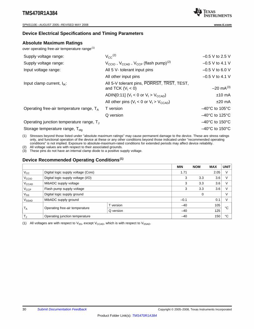
Device Electrical Specifications and Timing Parameters
Absolute Maximum Ratings
Device Recommended Operating Conditions (1)
TMS470R1A384
SPNS110E–AUGUST 2005–REVISED MAY 2008 ......................................................................................................................................................... www.ti.com
over operating free-air temperature range (1)
Supply voltage range: VCC(2) –0.5 V to 2.5 V
Supply voltage range: VCCIO , VCCAD , VCCP (flash pump) (2) –0.5 V to 4.1 VInput voltage range: All 5 V- tolerant input pins –0.5 V to 6.0 V
All other input pins –0.5 V to 4.1 VInput clamp current, IIK: All 5-V tolerant pins, PORRST, TRST, TEST,
and TCK (VI < 0) –20 mA (3)
ADIN[0:11] (VI < 0 or VI > VCCAD) ±10 mAAll other pins (VI < 0 or VI > VCCAD) ±20 mA
Operating free-air temperature range, TA T version –40°C to 105°CQ version –40°C to 125°C
Operating junction temperature range, TJ –40°C to 150°CStorage temperature range, Tstg –40°C to 150°C
(1) Stresses beyond those listed under "absolute maximum ratings" may cause permanent damage to the device. These are stress ratingsonly, and functional operation of the device at these or any other conditions beyond those indicated under "recommended operatingconditions" is not implied. Exposure to absolute-maximum-rated conditions for extended periods may affect device reliability.
(2) All voltage values are with respect to their associated grounds.(3) These pins do not have an internal clamp diode to a positive supply voltage.
MIN NOM MAX UNITVCC Digital logic supply voltage (Core) 1.71 2.05 VVCCIO Digital logic supply voltage (I/O) 3 3.3 3.6 VVCCAD MibADC supply voltage 3 3.3 3.6 VVCCP Flash pump supply voltage 3 3.3 3.6 VVSS Digital logic supply ground 0 VVSSAD MibADC supply ground –0.1 0.1 V
T version –40 105TA Operating free-air temperature °C
Q version –40 125TJ Operating junction temperature –40 150 °C
(1) All voltages are with respect to VSS, except VCCAD, which is with respect to VSSAD.
30 Submit Documentation Feedback Copyright © 2005–2008, Texas Instruments Incorporated
Product Folder Link(s): TMS470R1A384
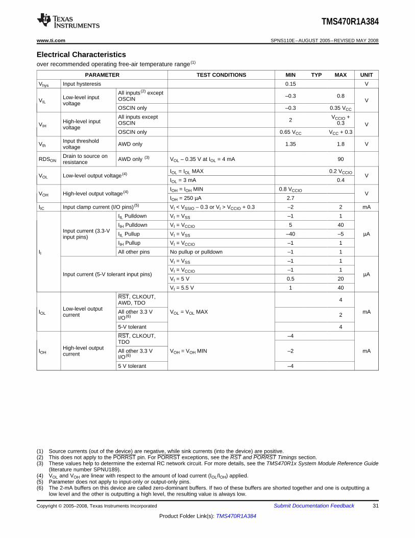
Electrical Characteristics
TMS470R1A384
www.ti.com ......................................................................................................................................................... SPNS110E–AUGUST 2005–REVISED MAY 2008
over recommended operating free-air temperature range (1)
PARAMETER TEST CONDITIONS MIN TYP MAX UNITVhys Input hysteresis 0.15 V
All inputs (2) except –0.3 0.8Low-level input OSCINVIL VvoltageOSCIN only –0.3 0.35 VCC
All inputs except VCCIO +2High-level input OSCIN 0.3VIH VvoltageOSCIN only 0.65 VCC VCC + 0.3
Input thresholdVth AWD only 1.35 1.8 VvoltageDrain to source onRDSON AWD only (3) VOL – 0.35 V at IOL = 4 mA 90resistance
IOL = IOL MAX 0.2 VCCIOVOL Low-level output voltage (4) VIOL = 3 mA 0.4IOH = IOH MIN 0.8 VCCIOVOH High-level output voltage (4) VIOH = 250 µA 2.7
IIC Input clamp current (I/O pins) (5) VI < VSSIO – 0.3 or VI > VCCIO + 0.3 –2 2 mAIIL Pulldown VI = VSS –1 1IIH Pulldown VI = VCCIO 5 40
Input current (3.3-V IIL Pullup VI = VSS –40 –5 µAinput pins)IIH Pullup VI = VCCIO –1 1
II All other pins No pullup or pulldown –1 1VI = VSS –1 1VI = VCCIO –1 1
Input current (5-V tolerant input pins) µAVI = 5 V 0.5 20VI = 5.5 V 1 40
RST, CLKOUT, 4AWD, TDOLow-level outputIOL All other 3.3 V VOL = VOL MAX mAcurrent 2I/O (6)
5-V tolerant 4RST, CLKOUT, –4TDO
High-level outputIOH All other 3.3 V VOH = VOH MIN –2 mAcurrent I/O (6)
5 V tolerant –4
(1) Source currents (out of the device) are negative, while sink currents (into the device) are positive.(2) This does not apply to the PORRST pin. For PORRST exceptions, see the RST and PORRST Timings section.(3) These values help to determine the external RC network circuit. For more details, see the TMS470R1x System Module Reference Guide
(literature number SPNU189).(4) VOL and VOH are linear with respect to the amount of load current (IOL/IOH) applied.(5) Parameter does not apply to input-only or output-only pins.(6) The 2-mA buffers on this device are called zero-dominant buffers. If two of these buffers are shorted together and one is outputting a
low level and the other is outputting a high level, the resulting value is always low.
Copyright © 2005–2008, Texas Instruments Incorporated Submit Documentation Feedback 31
Product Folder Link(s): TMS470R1A384
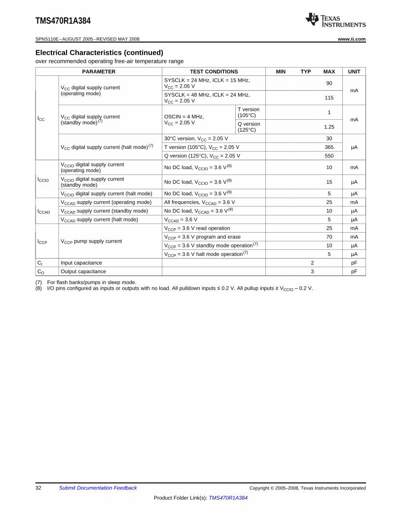
TMS470R1A384
SPNS110E–AUGUST 2005–REVISED MAY 2008 ......................................................................................................................................................... www.ti.com
Electrical Characteristics (continued)over recommended operating free-air temperature range
PARAMETER TEST CONDITIONS MIN TYP MAX UNITSYSCLK = 24 MHz, ICLK = 15 MHz, 90VCC = 2.05 VVCC digital supply current mA(operating mode) SYSCLK = 48 MHz, ICLK = 24 MHz, 115VCC = 2.05 V
T version 1(105°C)VCC digital supply current OSCIN = 4 MHz,ICC mA(standby mode) (7) VCC = 2.05 V Q version 1.25(125°C)30°C version, VCC = 2.05 V 30
VCC digital supply current (halt mode) (7) T version (105°C), VCC = 2.05 V 365 µAQ version (125°C), VCC = 2.05 V 550
VCCIO digital supply current No DC load, VCCIO = 3.6 V (8) 10 mA(operating mode)ICCIO VCCIO digital supply current No DC load, VCCIO = 3.6 V (8) 15 µA(standby mode)
VCCIO digital supply current (halt mode) No DC load, VCCIO = 3.6 V (8) 5 µAVCCAD supply current (operating mode) All frequencies, VCCAD = 3.6 V 25 mA
ICCAD VCCAD supply current (standby mode) No DC load, VCCAD = 3.6 V (8) 10 µAVCCAD supply current (halt mode) VCCAD = 3.6 V 5 µA
VCCP = 3.6 V read operation 25 mAVCCP = 3.6 V program and erase 70 mA
ICCP VCCP pump supply currentVCCP = 3.6 V standby mode operation (7) 10 µAVCCP = 3.6 V halt mode operation (7) 5 µA
CI Input capacitance 2 pFCO Output capacitance 3 pF
(7) For flash banks/pumps in sleep mode.(8) I/O pins configured as inputs or outputs with no load. All pulldown inputs ≤ 0.2 V. All pullup inputs ≥ VCCIO – 0.2 V.
32 Submit Documentation Feedback Copyright © 2005–2008, Texas Instruments Incorporated
Product Folder Link(s): TMS470R1A384

Parameter Measurement Information
Ω
Where: IOL = IOL MAX for the respective pin (A)
IOH = IOH MIN for the respective pin(A)
VLOAD = 1.5 VCL = 150-pF typical load-circuit capacitance(B)
TMS470R1A384
www.ti.com ......................................................................................................................................................... SPNS110E–AUGUST 2005–REVISED MAY 2008
A. For these values, see the "Electrical Characteristics over Recommended Operating Free-Air Temperature Range"table.
B. All timing parameters measured using an external load capacitance of 150 pF unless otherwise noted.
Figure 5. Test Load Circuit
Copyright © 2005–2008, Texas Instruments Incorporated Submit Documentation Feedback 33
Product Folder Link(s): TMS470R1A384
Timing Parameter Symbology
TMS470R1A384
SPNS110E–AUGUST 2005–REVISED MAY 2008 ......................................................................................................................................................... www.ti.com
Timing parameter symbols have been created in accordance with JEDEC Standard 100. To shorten the symbols,some of the pin names and other related terminology have been abbreviated as follows:
CM Compaction, CMPCT RD ReadCO CLKOUT RST Reset, RSTER Erase RX SCInRXICLK Interface clock S Slave modeM Master mode SCC SCInCLKOSC, OSCI OSCIN SIMO SPInSIMOOSCO OSCOUT SOMI SPInSOMIP Program, PROG SPC SPInCLKR Ready SYS System clockR0 Read margin 0, RDMRGN0 TX SCInTXR1 Read margin 1, RDMRGN1
Lowercase subscripts and their meanings are:
a access time r rise timec cycle time (period) su setup timed delay time t transition timef fall time v valid timeh hold time w pulse duration (width)
The following additional letters are used with these meanings:
H High X Unknown, changing, or don't care levelL Low Z High impedanceV Valid
34 Submit Documentation Feedback Copyright © 2005–2008, Texas Instruments Incorporated
Product Folder Link(s): TMS470R1A384
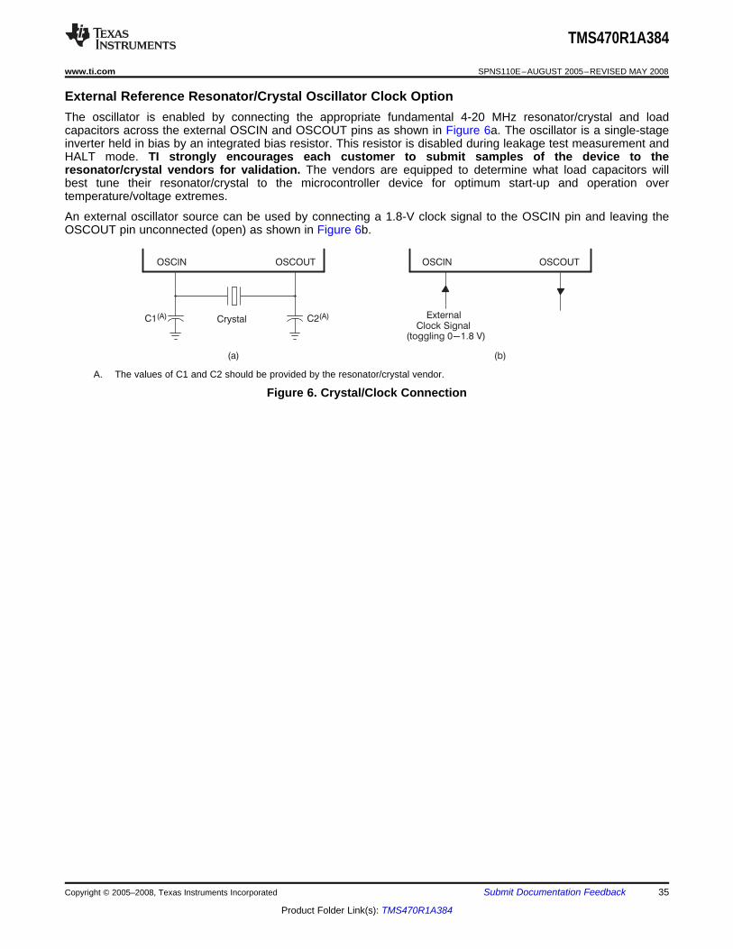
External Reference Resonator/Crystal Oscillator Clock Option
!
"
TMS470R1A384
www.ti.com ......................................................................................................................................................... SPNS110E–AUGUST 2005–REVISED MAY 2008
The oscillator is enabled by connecting the appropriate fundamental 4-20 MHz resonator/crystal and loadcapacitors across the external OSCIN and OSCOUT pins as shown in Figure 6a. The oscillator is a single-stageinverter held in bias by an integrated bias resistor. This resistor is disabled during leakage test measurement andHALT mode. TI strongly encourages each customer to submit samples of the device to theresonator/crystal vendors for validation. The vendors are equipped to determine what load capacitors willbest tune their resonator/crystal to the microcontroller device for optimum start-up and operation overtemperature/voltage extremes.
An external oscillator source can be used by connecting a 1.8-V clock signal to the OSCIN pin and leaving theOSCOUT pin unconnected (open) as shown in Figure 6b.
A. The values of C1 and C2 should be provided by the resonator/crystal vendor.
Figure 6. Crystal/Clock Connection
Copyright © 2005–2008, Texas Instruments Incorporated Submit Documentation Feedback 35
Product Folder Link(s): TMS470R1A384
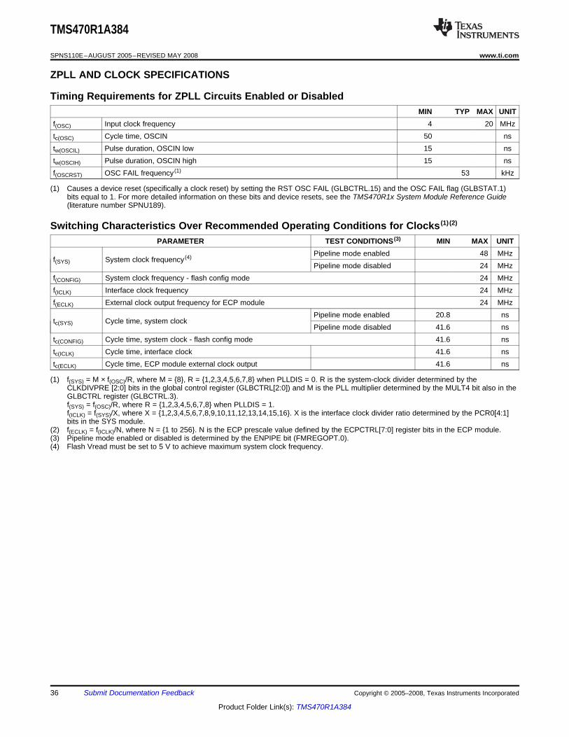
ZPLL AND CLOCK SPECIFICATIONS
Timing Requirements for ZPLL Circuits Enabled or Disabled
Switching Characteristics Over Recommended Operating Conditions for Clocks (1) (2)
TMS470R1A384
SPNS110E–AUGUST 2005–REVISED MAY 2008 ......................................................................................................................................................... www.ti.com
MIN TYP MAX UNITf(OSC) Input clock frequency 4 20 MHztc(OSC) Cycle time, OSCIN 50 nstw(OSCIL) Pulse duration, OSCIN low 15 nstw(OSCIH) Pulse duration, OSCIN high 15 nsf(OSCRST) OSC FAIL frequency (1) 53 kHz
(1) Causes a device reset (specifically a clock reset) by setting the RST OSC FAIL (GLBCTRL.15) and the OSC FAIL flag (GLBSTAT.1)bits equal to 1. For more detailed information on these bits and device resets, see the TMS470R1x System Module Reference Guide(literature number SPNU189).
PARAMETER TEST CONDITIONS (3) MIN MAX UNITPipeline mode enabled 48 MHz
f(SYS) System clock frequency (4)Pipeline mode disabled 24 MHz
f(CONFIG) System clock frequency - flash config mode 24 MHzf(ICLK) Interface clock frequency 24 MHzf(ECLK) External clock output frequency for ECP module 24 MHz
Pipeline mode enabled 20.8 nstc(SYS) Cycle time, system clock
Pipeline mode disabled 41.6 nstc(CONFIG) Cycle time, system clock - flash config mode 41.6 nstc(ICLK) Cycle time, interface clock 41.6 nstc(ECLK) Cycle time, ECP module external clock output 41.6 ns
(1) f(SYS) = M × f(OSC)/R, where M = 8, R = 1,2,3,4,5,6,7,8 when PLLDIS = 0. R is the system-clock divider determined by theCLKDIVPRE [2:0] bits in the global control register (GLBCTRL[2:0]) and M is the PLL multiplier determined by the MULT4 bit also in theGLBCTRL register (GLBCTRL.3).f(SYS) = f(OSC)/R, where R = 1,2,3,4,5,6,7,8 when PLLDIS = 1.f(ICLK) = f(SYS)/X, where X = 1,2,3,4,5,6,7,8,9,10,11,12,13,14,15,16. X is the interface clock divider ratio determined by the PCR0[4:1]bits in the SYS module.
(2) f(ECLK) = f(ICLK)/N, where N = 1 to 256. N is the ECP prescale value defined by the ECPCTRL[7:0] register bits in the ECP module.(3) Pipeline mode enabled or disabled is determined by the ENPIPE bit (FMREGOPT.0).(4) Flash Vread must be set to 5 V to achieve maximum system clock frequency.
36 Submit Documentation Feedback Copyright © 2005–2008, Texas Instruments Incorporated
Product Folder Link(s): TMS470R1A384
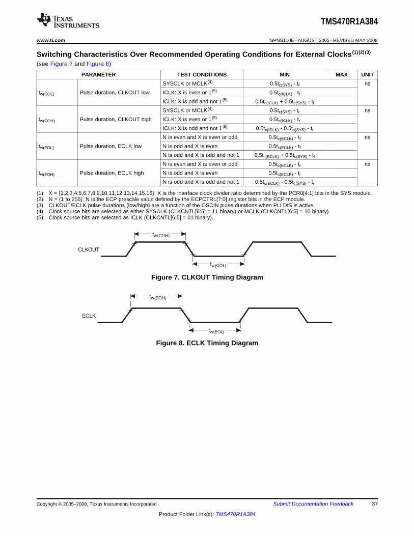
Switching Characteristics Over Recommended Operating Conditions for External Clocks (1) (2) (3)
TMS470R1A384
www.ti.com ......................................................................................................................................................... SPNS110E–AUGUST 2005–REVISED MAY 2008
(see Figure 7 and Figure 8)
PARAMETER TEST CONDITIONS MIN MAX UNITSYSCLK or MCLK (4) 0.5tc(SYS) - tf ns
tw(COL) Pulse duration, CLKOUT low ICLK: X is even or 1 (5) 0.5tc(ICLK) - tfICLK: X is odd and not 1 (5) 0.5tc(ICLK) + 0.5tc(SYS) - tfSYSCLK or MCLK (4) 0.5tc(SYS) - tr ns
tw(COH) Pulse duration, CLKOUT high ICLK: X is even or 1 (5) 0.5tc(ICLK) - trICLK: X is odd and not 1 (5) 0.5tc(ICLK) - 0.5tc(SYS) - trN is even and X is even or odd 0.5tc(ECLK) - tf ns
tw(EOL) Pulse duration, ECLK low N is odd and X is even 0.5tc(ECLK) - tfN is odd and X is odd and not 1 0.5tc(ECLK) + 0.5tc(SYS) - tfN is even and X is even or odd 0.5tc(ECLK) - tr ns
tw(EOH) Pulse duration, ECLK high N is odd and X is even 0.5tc(ECLK) - trN is odd and X is odd and not 1 0.5tc(ECLK) - 0.5tc(SYS) - tr
(1) X = 1,2,3,4,5,6,7,8,9,10,11,12,13,14,15,16. X is the interface clock divider ratio determined by the PCR0[4:1] bits in the SYS module.(2) N = 1 to 256. N is the ECP prescale value defined by the ECPCTRL[7:0] register bits in the ECP module.(3) CLKOUT/ECLK pulse durations (low/high) are a function of the OSCIN pulse durations when PLLDIS is active.(4) Clock source bits are selected as either SYSCLK (CLKCNTL[6:5] = 11 binary) or MCLK (CLKCNTL[6:5] = 10 binary).(5) Clock source bits are selected as ICLK (CLKCNTL[6:5] = 01 binary).
Figure 7. CLKOUT Timing Diagram
Figure 8. ECLK Timing Diagram
Copyright © 2005–2008, Texas Instruments Incorporated Submit Documentation Feedback 37
Product Folder Link(s): TMS470R1A384
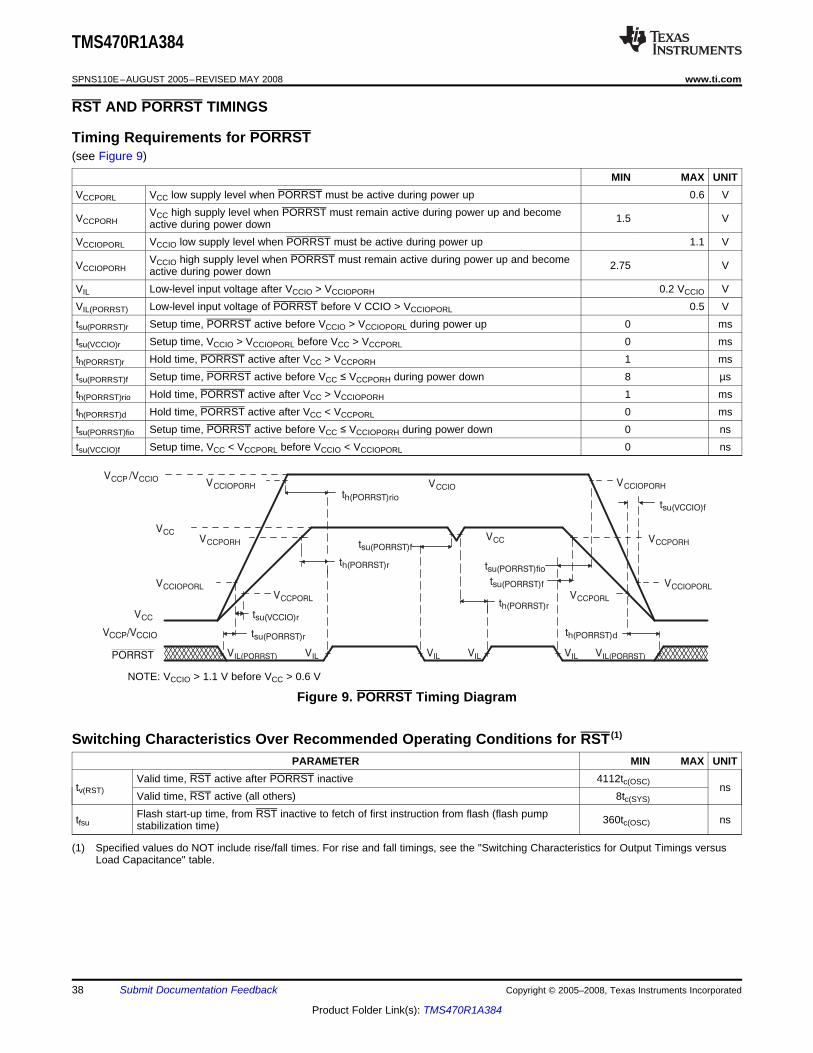
RST AND PORRST TIMINGS
Timing Requirements for PORRST
Switching Characteristics Over Recommended Operating Conditions for RST (1)
TMS470R1A384
SPNS110E–AUGUST 2005–REVISED MAY 2008 ......................................................................................................................................................... www.ti.com
(see Figure 9)
MIN MAX UNITVCCPORL VCC low supply level when PORRST must be active during power up 0.6 V
VCC high supply level when PORRST must remain active during power up and becomeVCCPORH 1.5 Vactive during power downVCCIOPORL VCCIO low supply level when PORRST must be active during power up 1.1 V
VCCIO high supply level when PORRST must remain active during power up and becomeVCCIOPORH 2.75 Vactive during power downVIL Low-level input voltage after VCCIO > VCCIOPORH 0.2 VCCIO VVIL(PORRST) Low-level input voltage of PORRST before V CCIO > VCCIOPORL 0.5 Vtsu(PORRST)r Setup time, PORRST active before VCCIO > VCCIOPORL during power up 0 mstsu(VCCIO)r Setup time, VCCIO > VCCIOPORL before VCC > VCCPORL 0 msth(PORRST)r Hold time, PORRST active after VCC > VCCPORH 1 mstsu(PORRST)f Setup time, PORRST active before VCC ≤ VCCPORH during power down 8 µsth(PORRST)rio Hold time, PORRST active after VCC > VCCIOPORH 1 msth(PORRST)d Hold time, PORRST active after VCC < VCCPORL 0 mstsu(PORRST)fio Setup time, PORRST active before VCC ≤ VCCIOPORH during power down 0 nstsu(VCCIO)f Setup time, VCC < VCCPORL before VCCIO < VCCIOPORL 0 ns
NOTE: VCCIO > 1.1 V before VCC > 0.6 V
Figure 9. PORRST Timing Diagram
PARAMETER MIN MAX UNITValid time, RST active after PORRST inactive 4112tc(OSC)tv(RST) nsValid time, RST active (all others) 8tc(SYS)
Flash start-up time, from RST inactive to fetch of first instruction from flash (flash pumptfsu 360tc(OSC) nsstabilization time)
(1) Specified values do NOT include rise/fall times. For rise and fall timings, see the "Switching Characteristics for Output Timings versusLoad Capacitance" table.
38 Submit Documentation Feedback Copyright © 2005–2008, Texas Instruments Incorporated
Product Folder Link(s): TMS470R1A384
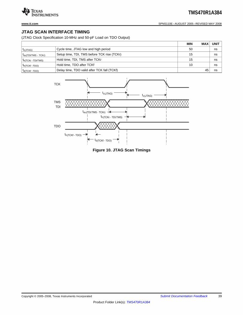
JTAG SCAN INTERFACE TIMING
TMS470R1A384
www.ti.com ......................................................................................................................................................... SPNS110E–AUGUST 2005–REVISED MAY 2008
(JTAG Clock Specification 10-MHz and 50-pF Load on TDO Output)
MIN MAX UNITtc(JTAG) Cycle time, JTAG low and high period 50 nstsu(TDI/TMS - TCKr) Setup time, TDI, TMS before TCK rise (TCKr) 15 nsth(TCKr -TDI/TMS) Hold time, TDI, TMS after TCKr 15 nsth(TCKf -TDO) Hold time, TDO after TCKf 10 nstd(TCKf -TDO) Delay time, TDO valid after TCK fall (TCKf) 45 ns
Figure 10. JTAG Scan Timings
Copyright © 2005–2008, Texas Instruments Incorporated Submit Documentation Feedback 39
Product Folder Link(s): TMS470R1A384
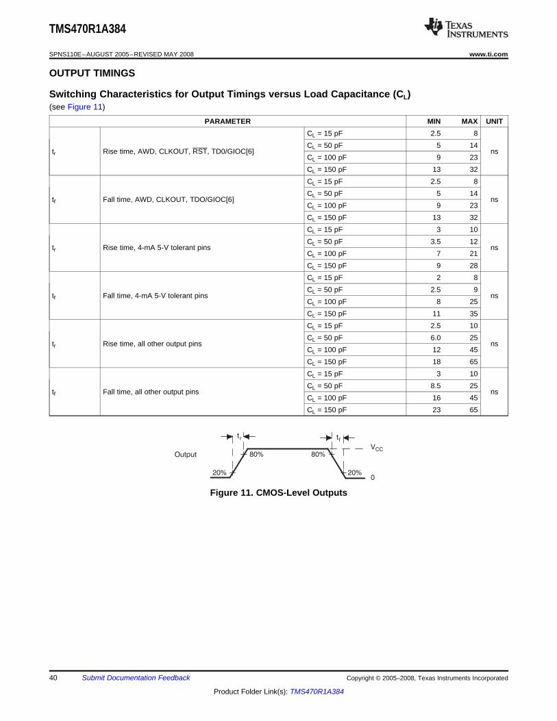
OUTPUT TIMINGS
Switching Characteristics for Output Timings versus Load Capacitance (CL)
TMS470R1A384
SPNS110E–AUGUST 2005–REVISED MAY 2008 ......................................................................................................................................................... www.ti.com
(see Figure 11)
PARAMETER MIN MAX UNITCL = 15 pF 2.5 8CL = 50 pF 5 14
tr Rise time, AWD, CLKOUT, RST, TD0/GIOC[6] nsCL = 100 pF 9 23CL = 150 pF 13 32CL = 15 pF 2.5 8CL = 50 pF 5 14
tf Fall time, AWD, CLKOUT, TDO/GIOC[6] nsCL = 100 pF 9 23CL = 150 pF 13 32CL = 15 pF 3 10CL = 50 pF 3.5 12
tr Rise time, 4-mA 5-V tolerant pins nsCL = 100 pF 7 21CL = 150 pF 9 28CL = 15 pF 2 8CL = 50 pF 2.5 9
tf Fall time, 4-mA 5-V tolerant pins nsCL = 100 pF 8 25CL = 150 pF 11 35CL = 15 pF 2.5 10CL = 50 pF 6.0 25
tr Rise time, all other output pins nsCL = 100 pF 12 45CL = 150 pF 18 65CL = 15 pF 3 10CL = 50 pF 8.5 25
tf Fall time, all other output pins nsCL = 100 pF 16 45CL = 150 pF 23 65
Figure 11. CMOS-Level Outputs
40 Submit Documentation Feedback Copyright © 2005–2008, Texas Instruments Incorporated
Product Folder Link(s): TMS470R1A384
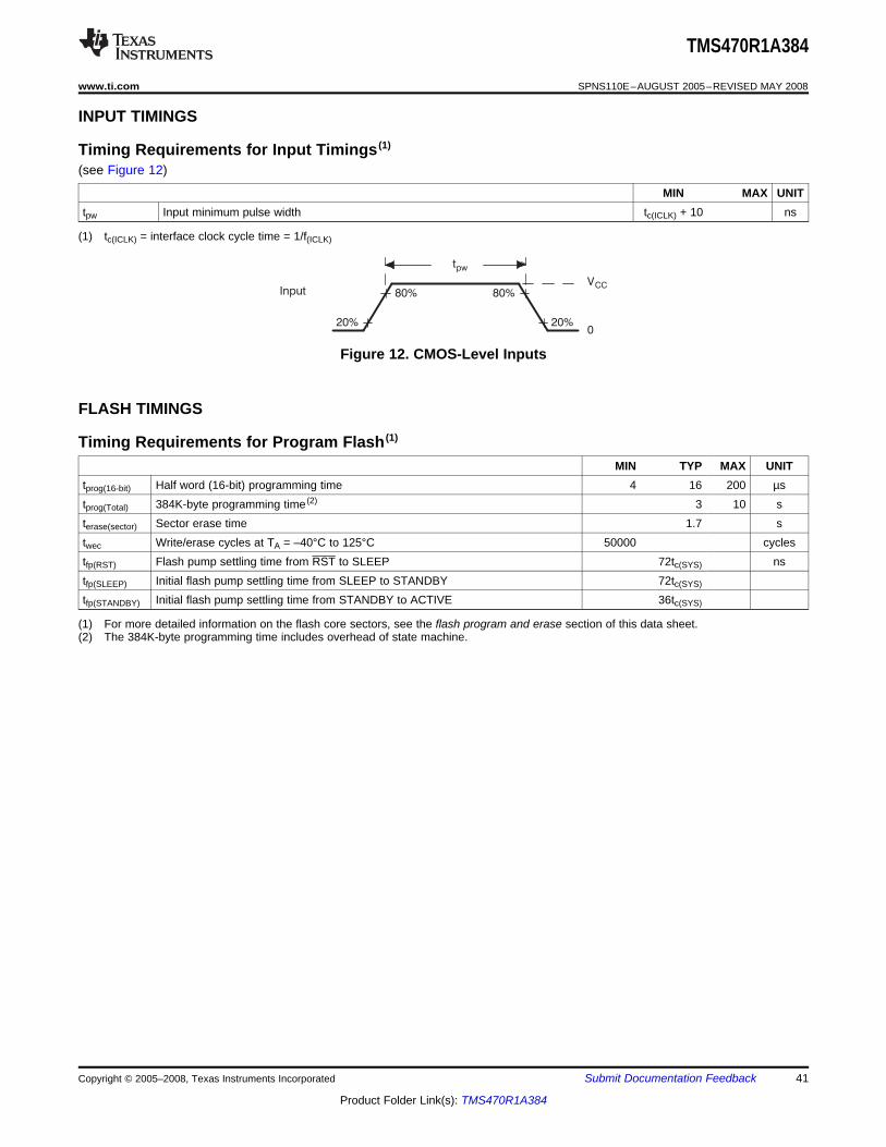
INPUT TIMINGS
Timing Requirements for Input Timings (1)
FLASH TIMINGS
Timing Requirements for Program Flash (1)
TMS470R1A384
www.ti.com ......................................................................................................................................................... SPNS110E–AUGUST 2005–REVISED MAY 2008
(see Figure 12)
MIN MAX UNITtpw Input minimum pulse width tc(ICLK) + 10 ns
(1) tc(ICLK) = interface clock cycle time = 1/f(ICLK)
Figure 12. CMOS-Level Inputs
MIN TYP MAX UNITtprog(16-bit) Half word (16-bit) programming time 4 16 200 µstprog(Total) 384K-byte programming time (2) 3 10 sterase(sector) Sector erase time 1.7 stwec Write/erase cycles at TA = –40°C to 125°C 50000 cyclestfp(RST) Flash pump settling time from RST to SLEEP 72tc(SYS) nstfp(SLEEP) Initial flash pump settling time from SLEEP to STANDBY 72tc(SYS)
tfp(STANDBY) Initial flash pump settling time from STANDBY to ACTIVE 36tc(SYS)
(1) For more detailed information on the flash core sectors, see the flash program and erase section of this data sheet.(2) The 384K-byte programming time includes overhead of state machine.
Copyright © 2005–2008, Texas Instruments Incorporated Submit Documentation Feedback 41
Product Folder Link(s): TMS470R1A384
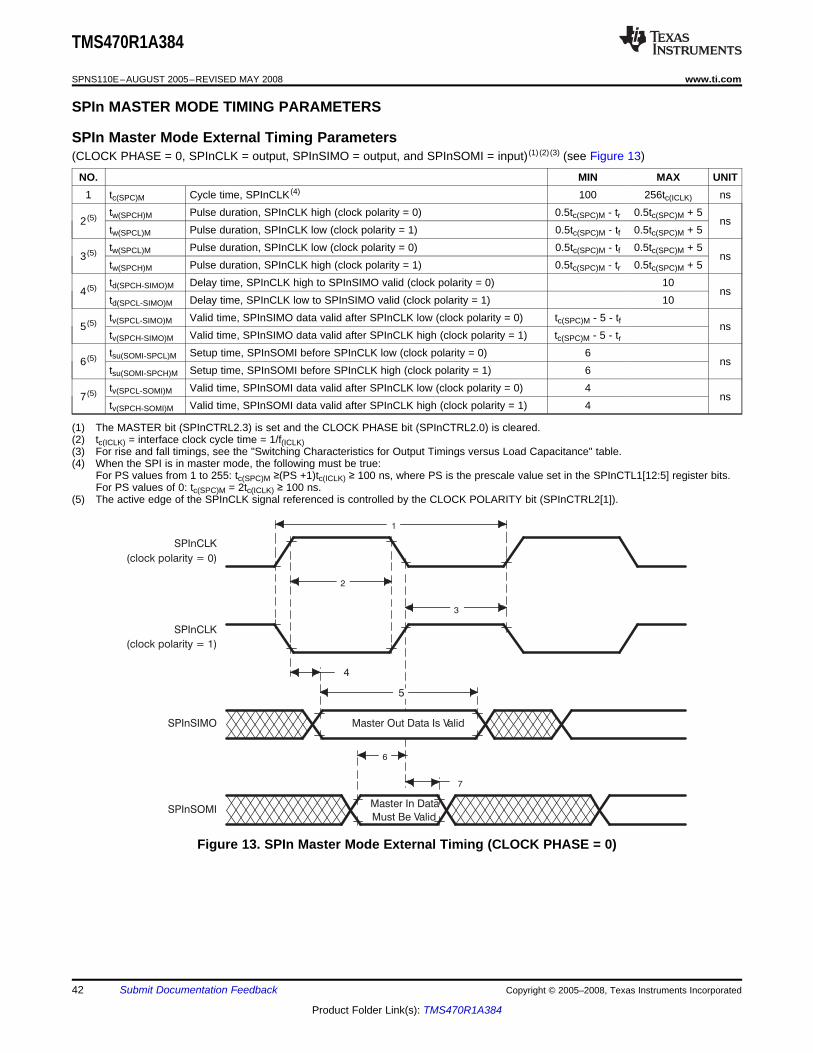
SPIn MASTER MODE TIMING PARAMETERS
SPIn Master Mode External Timing Parameters
! "$&
! "$&
#$"$
%#$
#$"%$$#
TMS470R1A384
SPNS110E–AUGUST 2005–REVISED MAY 2008 ......................................................................................................................................................... www.ti.com
(CLOCK PHASE = 0, SPInCLK = output, SPInSIMO = output, and SPInSOMI = input) (1) (2) (3) (see Figure 13)
NO. MIN MAX UNIT1 tc(SPC)M Cycle time, SPInCLK (4) 100 256tc(ICLK) ns
tw(SPCH)M Pulse duration, SPInCLK high (clock polarity = 0) 0.5tc(SPC)M - tr 0.5tc(SPC)M + 52 (5) ns
tw(SPCL)M Pulse duration, SPInCLK low (clock polarity = 1) 0.5tc(SPC)M - tf 0.5tc(SPC)M + 5tw(SPCL)M Pulse duration, SPInCLK low (clock polarity = 0) 0.5tc(SPC)M - tf 0.5tc(SPC)M + 5
3 (5) nstw(SPCH)M Pulse duration, SPInCLK high (clock polarity = 1) 0.5tc(SPC)M - tr 0.5tc(SPC)M + 5td(SPCH-SIMO)M Delay time, SPInCLK high to SPInSIMO valid (clock polarity = 0) 10
4 (5) nstd(SPCL-SIMO)M Delay time, SPInCLK low to SPInSIMO valid (clock polarity = 1) 10tv(SPCL-SIMO)M Valid time, SPInSIMO data valid after SPInCLK low (clock polarity = 0) tc(SPC)M - 5 - tf5 (5) nstv(SPCH-SIMO)M Valid time, SPInSIMO data valid after SPInCLK high (clock polarity = 1) tc(SPC)M - 5 - trtsu(SOMI-SPCL)M Setup time, SPInSOMI before SPInCLK low (clock polarity = 0) 6
6 (5) nstsu(SOMI-SPCH)M Setup time, SPInSOMI before SPInCLK high (clock polarity = 1) 6tv(SPCL-SOMI)M Valid time, SPInSOMI data valid after SPInCLK low (clock polarity = 0) 4
7 (5) nstv(SPCH-SOMI)M Valid time, SPInSOMI data valid after SPInCLK high (clock polarity = 1) 4
(1) The MASTER bit (SPInCTRL2.3) is set and the CLOCK PHASE bit (SPInCTRL2.0) is cleared.(2) tc(ICLK) = interface clock cycle time = 1/f(ICLK)(3) For rise and fall timings, see the "Switching Characteristics for Output Timings versus Load Capacitance" table.(4) When the SPI is in master mode, the following must be true:
For PS values from 1 to 255: tc(SPC)M ≥(PS +1)tc(ICLK) ≥ 100 ns, where PS is the prescale value set in the SPInCTL1[12:5] register bits.For PS values of 0: tc(SPC)M = 2tc(ICLK) ≥ 100 ns.
(5) The active edge of the SPInCLK signal referenced is controlled by the CLOCK POLARITY bit (SPInCTRL2[1]).
Figure 13. SPIn Master Mode External Timing (CLOCK PHASE = 0)
42 Submit Documentation Feedback Copyright © 2005–2008, Texas Instruments Incorporated
Product Folder Link(s): TMS470R1A384
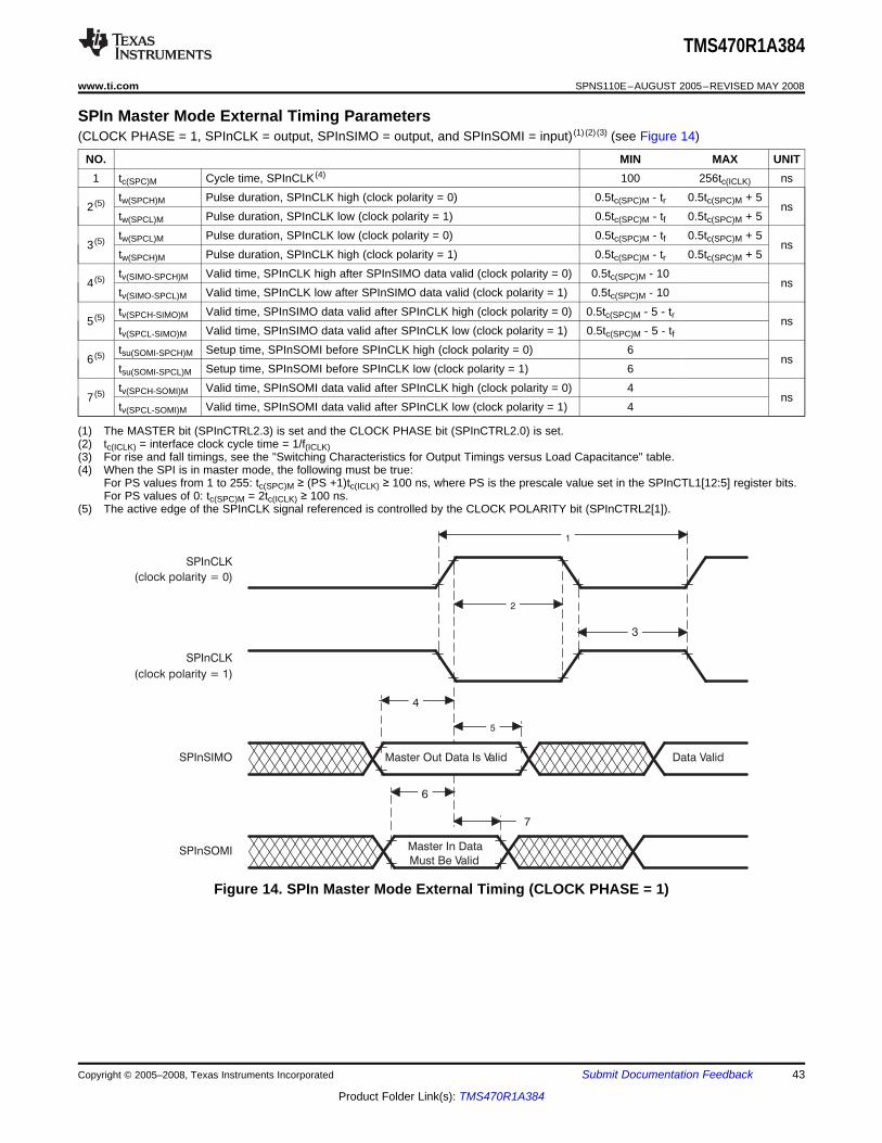
SPIn Master Mode External Timing Parameters
$
! "$&
! "$&
#$"$
%#$
#$"%$$#
TMS470R1A384
www.ti.com ......................................................................................................................................................... SPNS110E–AUGUST 2005–REVISED MAY 2008
(CLOCK PHASE = 1, SPInCLK = output, SPInSIMO = output, and SPInSOMI = input) (1) (2) (3) (see Figure 14)
NO. MIN MAX UNIT1 tc(SPC)M Cycle time, SPInCLK (4) 100 256tc(ICLK) ns
tw(SPCH)M Pulse duration, SPInCLK high (clock polarity = 0) 0.5tc(SPC)M - tr 0.5tc(SPC)M + 52 (5) ns
tw(SPCL)M Pulse duration, SPInCLK low (clock polarity = 1) 0.5tc(SPC)M - tf 0.5tc(SPC)M + 5tw(SPCL)M Pulse duration, SPInCLK low (clock polarity = 0) 0.5tc(SPC)M - tf 0.5tc(SPC)M + 5
3 (5) nstw(SPCH)M Pulse duration, SPInCLK high (clock polarity = 1) 0.5tc(SPC)M - tr 0.5tc(SPC)M + 5tv(SIMO-SPCH)M Valid time, SPInCLK high after SPInSIMO data valid (clock polarity = 0) 0.5tc(SPC)M - 10
4 (5) nstv(SIMO-SPCL)M Valid time, SPInCLK low after SPInSIMO data valid (clock polarity = 1) 0.5tc(SPC)M - 10tv(SPCH-SIMO)M Valid time, SPInSIMO data valid after SPInCLK high (clock polarity = 0) 0.5tc(SPC)M - 5 - tr5 (5) nstv(SPCL-SIMO)M Valid time, SPInSIMO data valid after SPInCLK low (clock polarity = 1) 0.5tc(SPC)M - 5 - tftsu(SOMI-SPCH)M Setup time, SPInSOMI before SPInCLK high (clock polarity = 0) 6
6 (5) nstsu(SOMI-SPCL)M Setup time, SPInSOMI before SPInCLK low (clock polarity = 1) 6tv(SPCH-SOMI)M Valid time, SPInSOMI data valid after SPInCLK high (clock polarity = 0) 4
7 (5) nstv(SPCL-SOMI)M Valid time, SPInSOMI data valid after SPInCLK low (clock polarity = 1) 4
(1) The MASTER bit (SPInCTRL2.3) is set and the CLOCK PHASE bit (SPInCTRL2.0) is set.(2) tc(ICLK) = interface clock cycle time = 1/f(ICLK)(3) For rise and fall timings, see the "Switching Characteristics for Output Timings versus Load Capacitance" table.(4) When the SPI is in master mode, the following must be true:
For PS values from 1 to 255: tc(SPC)M ≥ (PS +1)tc(ICLK) ≥ 100 ns, where PS is the prescale value set in the SPInCTL1[12:5] register bits.For PS values of 0: tc(SPC)M = 2tc(ICLK) ≥ 100 ns.
(5) The active edge of the SPInCLK signal referenced is controlled by the CLOCK POLARITY bit (SPInCTRL2[1]).
Figure 14. SPIn Master Mode External Timing (CLOCK PHASE = 1)
Copyright © 2005–2008, Texas Instruments Incorporated Submit Documentation Feedback 43
Product Folder Link(s): TMS470R1A384
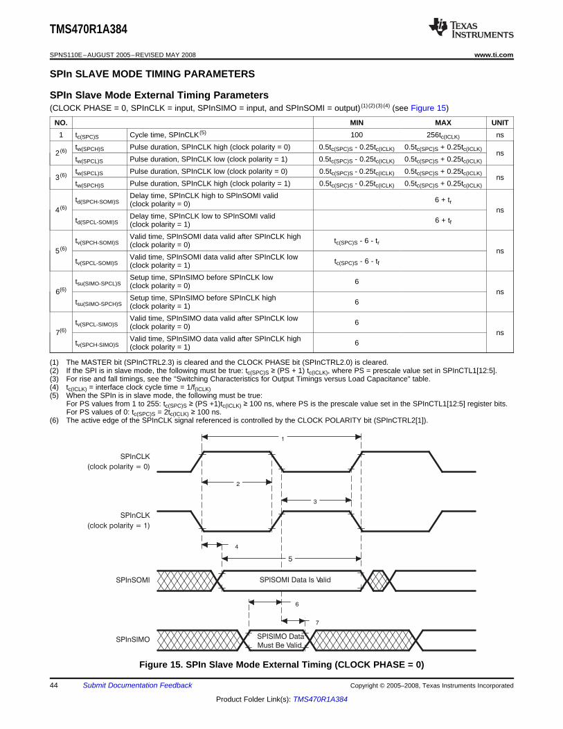
SPIn SLAVE MODE TIMING PARAMETERS
SPIn Slave Mode External Timing Parameters
! "$&
! "$&
$
%#$
$#
TMS470R1A384
SPNS110E–AUGUST 2005–REVISED MAY 2008 ......................................................................................................................................................... www.ti.com
(CLOCK PHASE = 0, SPInCLK = input, SPInSIMO = input, and SPInSOMI = output) (1) (2) (3) (4) (see Figure 15)
NO. MIN MAX UNIT1 tc(SPC)S Cycle time, SPInCLK (5) 100 256tc(ICLK) ns
tw(SPCH)S Pulse duration, SPInCLK high (clock polarity = 0) 0.5tc(SPC)S - 0.25tc(ICLK) 0.5tc(SPC)S + 0.25tc(ICLK)2 (6) nstw(SPCL)S Pulse duration, SPInCLK low (clock polarity = 1) 0.5tc(SPC)S - 0.25tc(ICLK) 0.5tc(SPC)S + 0.25tc(ICLK)
tw(SPCL)S Pulse duration, SPInCLK low (clock polarity = 0) 0.5tc(SPC)S - 0.25tc(ICLK) 0.5tc(SPC)S + 0.25tc(ICLK)3 (6) nstw(SPCH)S Pulse duration, SPInCLK high (clock polarity = 1) 0.5tc(SPC)S - 0.25tc(ICLK) 0.5tc(SPC)S + 0.25tc(ICLK)
Delay time, SPInCLK high to SPInSOMI validtd(SPCH-SOMI)S 6 + tr(clock polarity = 0)4 (6) ns
Delay time, SPInCLK low to SPInSOMI validtd(SPCL-SOMI)S 6 + tf(clock polarity = 1)Valid time, SPInSOMI data valid after SPInCLK hightv(SPCH-SOMI)S tc(SPC)S - 6 - tr(clock polarity = 0)
5 (6) nsValid time, SPInSOMI data valid after SPInCLK lowtv(SPCL-SOMI)S tc(SPC)S - 6 - tf(clock polarity = 1)Setup time, SPInSIMO before SPInCLK lowtsu(SIMO-SPCL)S 6(clock polarity = 0)
6(6) nsSetup time, SPInSIMO before SPInCLK hightsu(SIMO-SPCH)S 6(clock polarity = 1)Valid time, SPInSIMO data valid after SPInCLK lowtv(SPCL-SIMO)S 6(clock polarity = 0)
7(6) nsValid time, SPInSIMO data valid after SPInCLK hightv(SPCH-SIMO)S 6(clock polarity = 1)
(1) The MASTER bit (SPInCTRL2.3) is cleared and the CLOCK PHASE bit (SPInCTRL2.0) is cleared.(2) If the SPI is in slave mode, the following must be true: tc(SPC)S ≥ (PS + 1) tc(ICLK), where PS = prescale value set in SPInCTL1[12:5].(3) For rise and fall timings, see the "Switching Characteristics for Output Timings versus Load Capacitance" table.(4) tc(ICLK) = interface clock cycle time = 1/f(ICLK)(5) When the SPIn is in slave mode, the following must be true:
For PS values from 1 to 255: tc(SPC)S ≥ (PS +1)tc(ICLK) ≥ 100 ns, where PS is the prescale value set in the SPInCTL1[12:5] register bits.For PS values of 0: tc(SPC)S = 2tc(ICLK) ≥ 100 ns.
(6) The active edge of the SPInCLK signal referenced is controlled by the CLOCK POLARITY bit (SPInCTRL2[1]).
Figure 15. SPIn Slave Mode External Timing (CLOCK PHASE = 0)
44 Submit Documentation Feedback Copyright © 2005–2008, Texas Instruments Incorporated
Product Folder Link(s): TMS470R1A384
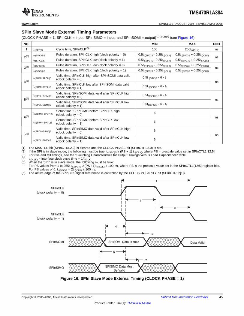
SPIn Slave Mode External Timing Parameters
$
! "$&
! "$&
$%#$
$#
TMS470R1A384
www.ti.com ......................................................................................................................................................... SPNS110E–AUGUST 2005–REVISED MAY 2008
(CLOCK PHASE = 1, SPInCLK = input, SPInSIMO = input, and SPInSOMI = output) (1) (2) (3) (4) (see Figure 16)
NO. MIN MAX UNIT1 tc(SPC)S Cycle time, SPInCLK (5) 100 256tc(ICLK) ns
tw(SPCH)S Pulse duration, SPInCLK high (clock polarity = 0) 0.5tc(SPC)S - 0.25tc(ICLK) 0.5tc(SPC)S + 0.25tc(ICLK)2 (6) nstw(SPCL)S Pulse duration, SPInCLK low (clock polarity = 1) 0.5tc(SPC)S - 0.25tc(ICLK) 0.5tc(SPC)S + 0.25tc(ICLK)
tw(SPCL)S Pulse duration, SPInCLK low (clock polarity = 0) 0.5tc(SPC)S - 0.25tc(ICLK) 0.5tc(SPC)S + 0.25tc(ICLK)3 (6) nstw(SPCH)S Pulse duration, SPInCLK high (clock polarity = 1) 0.5tc(SPC)S - 0.25tc(ICLK) 0.5tc(SPC)S + 0.25tc(ICLK)
Valid time, SPInCLK high after SPInSOMI data validtv(SOMI-SPCH)S 0.5tc(SPC)S - 6 - tr(clock polarity = 0)4 (6) ns
Valid time, SPInCLK low after SPInSOMI data validtv(SOMI-SPCL)S 0.5tc(SPC)S - 6 - tf(clock polarity = 1)Valid time, SPInSOMI data valid after SPInCLK hightv(SPCH-SOMI)S 0.5tc(SPC)S - 6 - tr(clock polarity = 0)
5 (6) nsValid time, SPInSOMI data valid after SPInCLK lowtv(SPCL-SOMI)S 0.5tc(SPC)S - 6 - tf(clock polarity = 1)Setup time, SPInSIMO before SPInCLK hightsu(SIMO-SPCH)S 6(clock polarity = 0)
6(6) nsSetup time, SPInSIMO before SPInCLK lowtsu(SIMO-SPCL)S 6(clock polarity = 1)Valid time, SPInSIMO data valid after SPInCLK hightv(SPCH-SIMO)S 6(clock polarity = 0)
7(6) nsValid time, SPInSIMO data valid after SPInCLK lowtv(SPCL-SIMO)S 6(clock polarity = 1)
(1) The MASTER bit (SPInCTRL2.3) is cleared and the CLOCK PHASE bit (SPInCTRL2.0) is set.(2) If the SPI is in slave mode, the following must be true: tc(SPC)S ≥ (PS + 1) tc(ICLK), where PS = prescale value set in SPInCTL1[12:5].(3) For rise and fall timings, see the "Switching Characteristics for Output Timings versus Load Capacitance" table.(4) tc(ICLK) = interface clock cycle time = 1/f(ICLK)(5) When the SPIn is in slave mode, the following must be true:
For PS values from 1 to 255: tc(SPC)S ≥ (PS +1)tc(ICLK) ≥ 100 ns, where PS is the prescale value set in the SPInCTL1[12:5] register bits.For PS values of 0: tc(SPC)S = 2tc(ICLK) ≥ 100 ns.
(6) The active edge of the SPInCLK signal referenced is controlled by the CLOCK POLARITY bit (SPInCTRL2[1]).
Figure 16. SPIn Slave Mode External Timing (CLOCK PHASE = 1)
Copyright © 2005–2008, Texas Instruments Incorporated Submit Documentation Feedback 45
Product Folder Link(s): TMS470R1A384
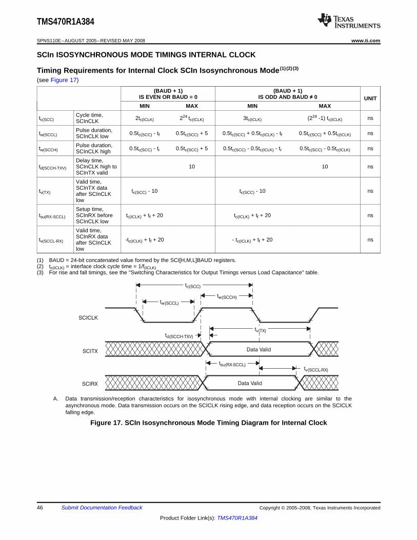
SCIn ISOSYNCHRONOUS MODE TIMINGS INTERNAL CLOCK
Timing Requirements for Internal Clock SCIn Isosynchronous Mode (1) (2) (3)
TMS470R1A384
SPNS110E–AUGUST 2005–REVISED MAY 2008 ......................................................................................................................................................... www.ti.com
(see Figure 17)
(BAUD + 1) (BAUD + 1)IS EVEN OR BAUD = 0 IS ODD AND BAUD ≠ 0 UNITMIN MAX MIN MAX
Cycle time,tc(SCC) 2tc(ICLK) 224 tc(ICLK) 3tc(ICLK) (224 -1) tc(ICLK) nsSCInCLKPulse duration,tw(SCCL) 0.5tc(SCC) - tf 0.5tc(SCC) + 5 0.5tc(SCC) + 0.5tc(ICLK) - tf 0.5tc(SCC) + 0.5tc(ICLK) nsSCInCLK lowPulse duration,tw(SCCH) 0.5tc(SCC) - tr 0.5tc(SCC) + 5 0.5tc(SCC) - 0.5tc(ICLK) - tr 0.5tc(SCC) - 0.5tc(ICLK) nsSCInCLK highDelay time,
td(SCCH-TXV) SCInCLK high to 10 10 nsSCInTX validValid time,SCInTX datatv(TX) tc(SCC) - 10 tc(SCC) - 10 nsafter SCInCLKlowSetup time,
tsu(RX-SCCL) SCInRX before tc(ICLK) + tf + 20 tc(ICLK) + tf + 20 nsSCInCLK lowValid time,SCInRX datatv(SCCL-RX) -tc(ICLK) + tf + 20 - tc(ICLK) + tf + 20 nsafter SCInCLKlow
(1) BAUD = 24-bit concatenated value formed by the SCI[H,M,L]BAUD registers.(2) tc(ICLK) = interface clock cycle time = 1/f(ICLK)(3) For rise and fall timings, see the "Switching Characteristics for Output Timings versus Load Capacitance" table.
A. Data transmission/reception characteristics for isosynchronous mode with internal clocking are similar to theasynchronous mode. Data transmission occurs on the SCICLK rising edge, and data reception occurs on the SCICLKfalling edge.
Figure 17. SCIn Isosynchronous Mode Timing Diagram for Internal Clock
46 Submit Documentation Feedback Copyright © 2005–2008, Texas Instruments Incorporated
Product Folder Link(s): TMS470R1A384
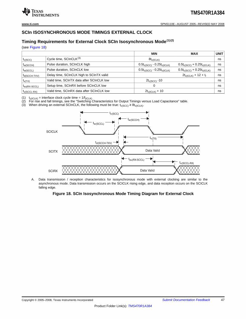
SCIn ISOSYNCHRONOUS MODE TIMINGS EXTERNAL CLOCK
Timing Requirements for External Clock SCIn Isosynchronous Mode (1) (2)
TMS470R1A384
www.ti.com ......................................................................................................................................................... SPNS110E–AUGUST 2005–REVISED MAY 2008
(see Figure 18)
MIN MAX UNITtc(SCC) Cycle time, SCInCLK (3) 8tc(ICLK) nstw(SCCH) Pulse duration, SCInCLK high 0.5tc(SCC) - 0.25tc(ICLK) 0.5tc(SCC) + 0.25tc(ICLK) nstw(SCCL) Pulse duration, SCInCLK low 0.5tc(SCC) - 0.25tc(ICLK) 0.5tc(SCC) + 0.25tc(ICLK) nstd(SCCH-TXV) Delay time, SCInCLK high to SCInTX valid 2tc(ICLK) + 12 + tr nstv(TX) Valid time, SCInTX data after SCInCLK low 2tc(SCC) -10 nstsu(RX-SCCL) Setup time, SCInRX before SCInCLK low 0 nstv(SCCL-RX) Valid time, SCInRX data after SCInCLK low 2tc(ICLK) + 10 ns
(1) tc(ICLK) = interface clock cycle time = 1/f(ICLK)(2) For rise and fall timings, see the "Switching Characteristics for Output Timings versus Load Capacitance" table.(3) When driving an external SCInCLK, the following must be true: tc(SCC) ≥ 8tc(ICLK).
A. Data transmission / reception characteristics for isosynchronous mode with external clocking are similar to theasynchronous mode. Data transmission occurs on the SCICLK rising edge, and data reception occurs on the SCICLKfalling edge.
Figure 18. SCIn Isosynchronous Mode Timing Diagram for External Clock
Copyright © 2005–2008, Texas Instruments Incorporated Submit Documentation Feedback 47
Product Folder Link(s): TMS470R1A384
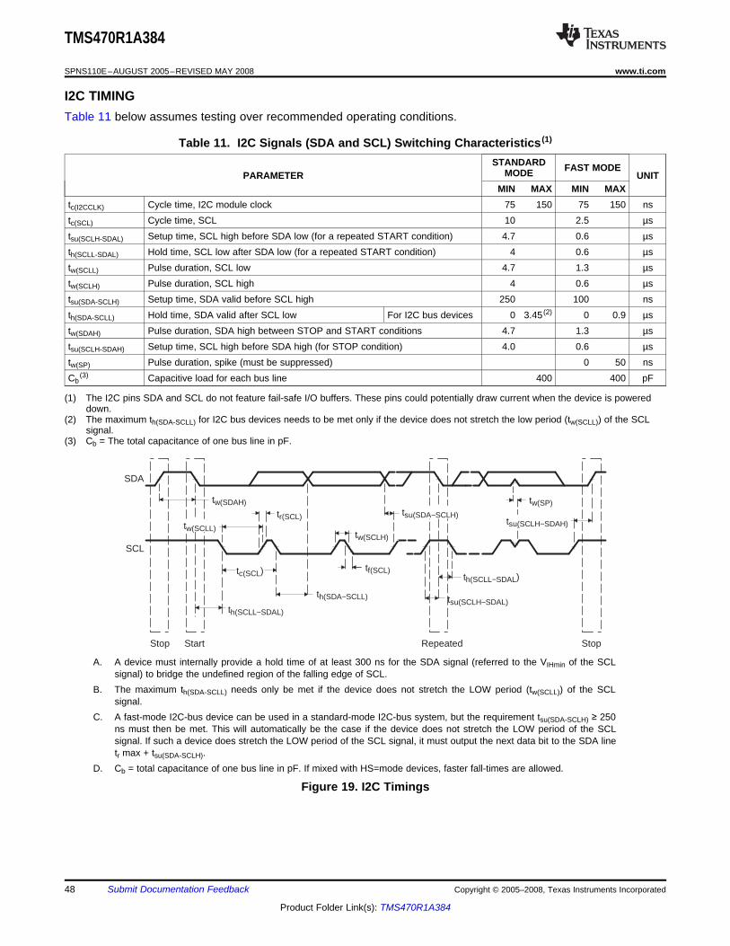
I2C TIMING
tw(SDAH)
tr(SCL)
th(SDA−SCLL)
th(SCLL−SDAL)
tw(SCLH)
tf(SCL)th(SCLL−SDAL)
tsu(SCLH−SDAL)
tw(SP)
tsu(SCLH−SDAH)
SDA
SCL
Stop Start Repeated Stop
tc(SCL)
tw(SCLL)
tsu(SDA−SCLH)
TMS470R1A384
SPNS110E–AUGUST 2005–REVISED MAY 2008 ......................................................................................................................................................... www.ti.com
Table 11 below assumes testing over recommended operating conditions.
Table 11. I2C Signals (SDA and SCL) Switching Characteristics (1)
STANDARD FAST MODEMODEPARAMETER UNITMIN MAX MIN MAX
tc(I2CCLK) Cycle time, I2C module clock 75 150 75 150 nstc(SCL) Cycle time, SCL 10 2.5 µstsu(SCLH-SDAL) Setup time, SCL high before SDA low (for a repeated START condition) 4.7 0.6 µsth(SCLL-SDAL) Hold time, SCL low after SDA low (for a repeated START condition) 4 0.6 µstw(SCLL) Pulse duration, SCL low 4.7 1.3 µstw(SCLH) Pulse duration, SCL high 4 0.6 µstsu(SDA-SCLH) Setup time, SDA valid before SCL high 250 100 nsth(SDA-SCLL) Hold time, SDA valid after SCL low For I2C bus devices 0 3.45 (2) 0 0.9 µstw(SDAH) Pulse duration, SDA high between STOP and START conditions 4.7 1.3 µstsu(SCLH-SDAH) Setup time, SCL high before SDA high (for STOP condition) 4.0 0.6 µstw(SP) Pulse duration, spike (must be suppressed) 0 50 nsCb
(3) Capacitive load for each bus line 400 400 pF
(1) The I2C pins SDA and SCL do not feature fail-safe I/O buffers. These pins could potentially draw current when the device is powereddown.
(2) The maximum th(SDA-SCLL) for I2C bus devices needs to be met only if the device does not stretch the low period (tw(SCLL)) of the SCLsignal.
(3) Cb = The total capacitance of one bus line in pF.
A. A device must internally provide a hold time of at least 300 ns for the SDA signal (referred to the VIHmin of the SCLsignal) to bridge the undefined region of the falling edge of SCL.
B. The maximum th(SDA-SCLL) needs only be met if the device does not stretch the LOW period (tw(SCLL)) of the SCLsignal.
C. A fast-mode I2C-bus device can be used in a standard-mode I2C-bus system, but the requirement tsu(SDA-SCLH) ≥ 250ns must then be met. This will automatically be the case if the device does not stretch the LOW period of the SCLsignal. If such a device does stretch the LOW period of the SCL signal, it must output the next data bit to the SDA linetr max + tsu(SDA-SCLH).
D. Cb = total capacitance of one bus line in pF. If mixed with HS=mode devices, faster fall-times are allowed.
Figure 19. I2C Timings
48 Submit Documentation Feedback Copyright © 2005–2008, Texas Instruments Incorporated
Product Folder Link(s): TMS470R1A384
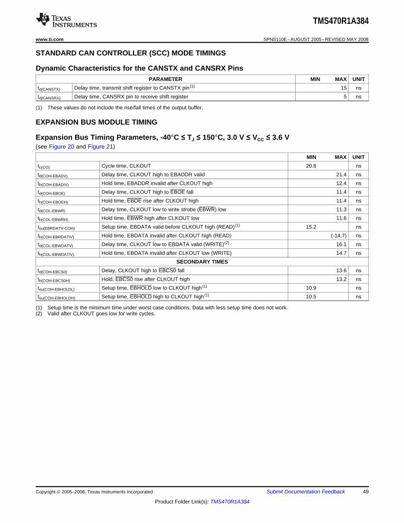
STANDARD CAN CONTROLLER (SCC) MODE TIMINGS
Dynamic Characteristics for the CANSTX and CANSRX Pins
EXPANSION BUS MODULE TIMING
Expansion Bus Timing Parameters, -40°C ≤ TJ ≤ 150°C, 3.0 V ≤ VCC ≤ 3.6 V
TMS470R1A384
www.ti.com ......................................................................................................................................................... SPNS110E–AUGUST 2005–REVISED MAY 2008
PARAMETER MIN MAX UNITtd(CANSTX) Delay time, transmit shift register to CANSTX pin (1) 15 nstd(CANSRX) Delay time, CANSRX pin to receive shift register 5 ns
(1) These values do not include the rise/fall times of the output buffer.
(see Figure 20 and Figure 21)
MIN MAX UNITtc(CO) Cycle time, CLKOUT 20.8 nstd(COH-EBADV) Delay time, CLKOUT high to EBADDR valid 21.4 nsth(COH-EBADIV) Hold time, EBADDR invalid after CLKOUT high 12.4 nstd(COH-EBOE) Delay time, CLKOUT high to EBOE fall 11.4 nsth(COH-EBOEH) Hold time, EBOE rise after CLKOUT high 11.4 nstd(COL-EBWR) Delay time, CLKOUT low to write strobe (EBWR) low 11.3 nsth(COL-EBWRH) Hold time, EBWR high after CLKOUT low 11.6 nstsu(EBRDATV-COH) Setup time, EBDATA valid before CLKOUT high (READ) (1) 15.2 nsth(COH-EBRDATIV) Hold time, EBDATA invalid after CLKOUT high (READ) (-14.7) nstd(COL-EBWDATV) Delay time, CLKOUT low to EBDATA valid (WRITE) (2) 16.1 nsth(COL-EBWDATIV) Hold time, EBDATA invalid after CLKOUT low (WRITE) 14.7 ns
SECONDARY TIMEStd(COH-EBCS0) Delay, CLKOUT high to EBCS0 fall 13.6 nsth(COH-EBCS0H) Hold, EBCS0 rise after CLKOUT high 13.2 nstsu(COH-EBHOLDL) Setup time, EBHOLD low to CLKOUT high (1) 10.9 nstsu(COH-EBHOLDH) Setup time, EBHOLD high to CLKOUT high (1) 10.5 ns
(1) Setup time is the minimum time under worst case conditions. Data with less setup time does not work.(2) Valid after CLKOUT goes low for write cycles.
Copyright © 2005–2008, Texas Instruments Incorporated Submit Documentation Feedback 49
Product Folder Link(s): TMS470R1A384
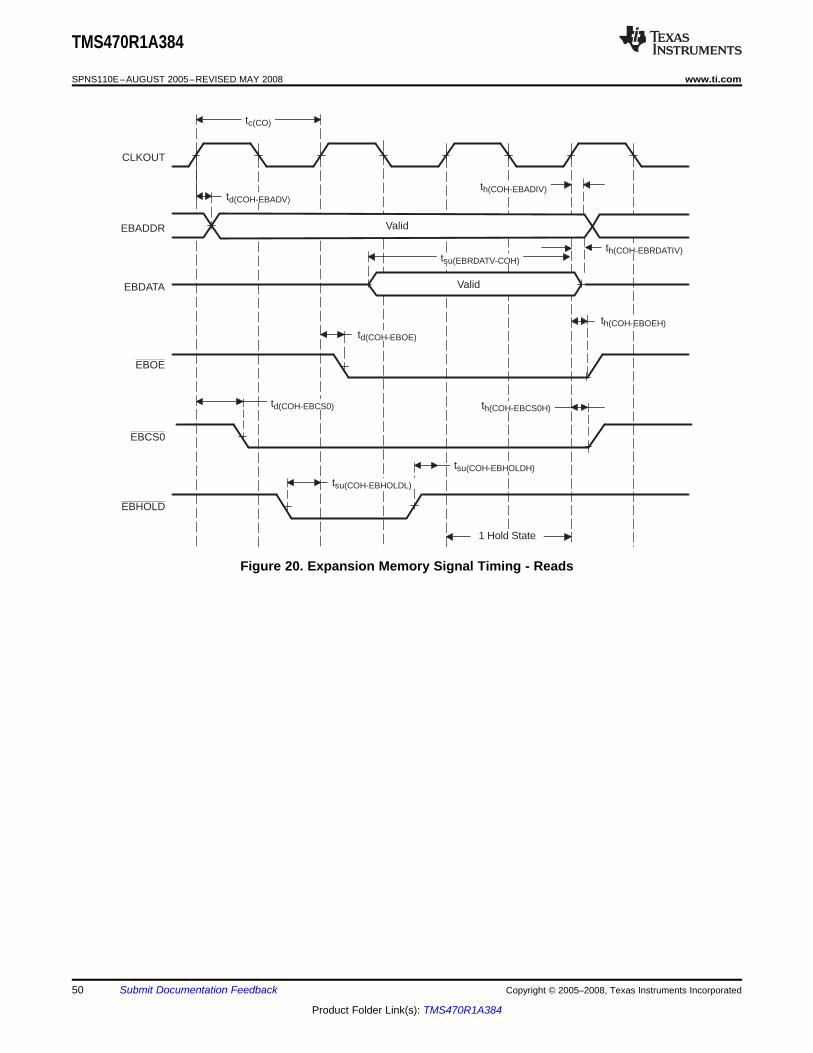
CLKOUT
EBADDR
EBDATA
EBOE
EBCS0
EBHOLD
1 Hold State
Valid
Valid
tc(CO)
td(COH-EBADV)th(COH-EBADIV)
tsu(EBRDATV-COH)th(COH-EBRDATIV)
td(COH-EBOE)
th(COH-EBOEH)
td(COH-EBCS0) th(COH-EBCS0H)
tsu(COH-EBHOLDL)
tsu(COH-EBHOLDH)
TMS470R1A384
SPNS110E–AUGUST 2005–REVISED MAY 2008 ......................................................................................................................................................... www.ti.com
Figure 20. Expansion Memory Signal Timing - Reads
50 Submit Documentation Feedback Copyright © 2005–2008, Texas Instruments Incorporated
Product Folder Link(s): TMS470R1A384
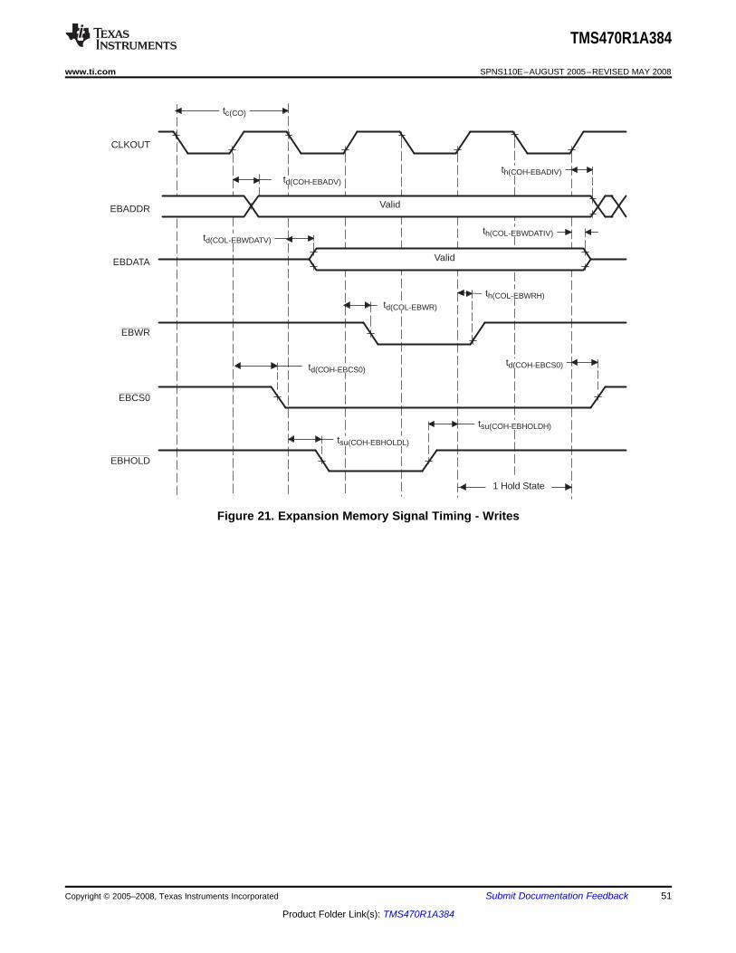
CLKOUT
EBADDR
EBDATA
EBWR
EBCS0
EBHOLD
1 Hold State
Valid
Valid
tc(CO)
td(COH-EBADV)
th(COH-EBADIV)
th(COL-EBWDATIV)
td(COL-EBWR)
th(COL-EBWRH)
td(COH-EBCS0)td(COH-EBCS0)
tsu(COH-EBHOLDL)
tsu(COH-EBHOLDH)
td(COL-EBWDATV)
TMS470R1A384
www.ti.com ......................................................................................................................................................... SPNS110E–AUGUST 2005–REVISED MAY 2008
Figure 21. Expansion Memory Signal Timing - Writes
Copyright © 2005–2008, Texas Instruments Incorporated Submit Documentation Feedback 51
Product Folder Link(s): TMS470R1A384
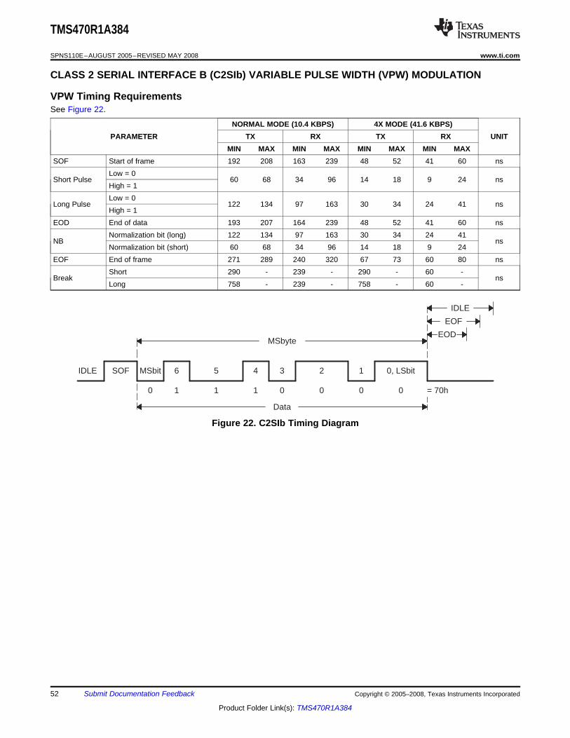
CLASS 2 SERIAL INTERFACE B (C2SIb) VARIABLE PULSE WIDTH (VPW) MODULATION
VPW Timing Requirements
MSbitIDLE SOF 6 5 4 3 2 1 0, LSbit
0 1 1 1 0 0 0 0 = 70h
Data
MSbyteEOD
EOF
IDLE
TMS470R1A384
SPNS110E–AUGUST 2005–REVISED MAY 2008 ......................................................................................................................................................... www.ti.com
See Figure 22.
NORMAL MODE (10.4 KBPS) 4X MODE (41.6 KBPS)PARAMETER TX RX TX RX UNIT
MIN MAX MIN MAX MIN MAX MIN MAXSOF Start of frame 192 208 163 239 48 52 41 60 ns
Low = 0Short Pulse 60 68 34 96 14 18 9 24 ns
High = 1Low = 0
Long Pulse 122 134 97 163 30 34 24 41 nsHigh = 1
EOD End of data 193 207 164 239 48 52 41 60 nsNormalization bit (long) 122 134 97 163 30 34 24 41
NB nsNormalization bit (short) 60 68 34 96 14 18 9 24
EOF End of frame 271 289 240 320 67 73 60 80 nsShort 290 - 239 - 290 - 60 -
Break nsLong 758 - 239 - 758 - 60 -
Figure 22. C2SIb Timing Diagram
52 Submit Documentation Feedback Copyright © 2005–2008, Texas Instruments Incorporated
Product Folder Link(s): TMS470R1A384
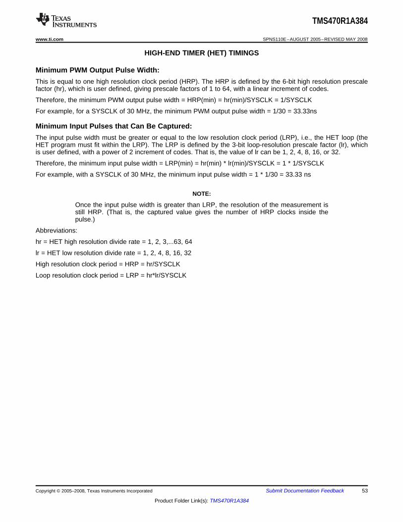
HIGH-END TIMER (HET) TIMINGS
Minimum PWM Output Pulse Width:
Minimum Input Pulses that Can Be Captured:
TMS470R1A384
www.ti.com ......................................................................................................................................................... SPNS110E–AUGUST 2005–REVISED MAY 2008
This is equal to one high resolution clock period (HRP). The HRP is defined by the 6-bit high resolution prescalefactor (hr), which is user defined, giving prescale factors of 1 to 64, with a linear increment of codes.
Therefore, the minimum PWM output pulse width = HRP(min) = hr(min)/SYSCLK = 1/SYSCLK
For example, for a SYSCLK of 30 MHz, the minimum PWM output pulse width = 1/30 = 33.33ns
The input pulse width must be greater or equal to the low resolution clock period (LRP), i.e., the HET loop (theHET program must fit within the LRP). The LRP is defined by the 3-bit loop-resolution prescale factor (lr), whichis user defined, with a power of 2 increment of codes. That is, the value of lr can be 1, 2, 4, 8, 16, or 32.
Therefore, the minimum input pulse width = LRP(min) = hr(min) * lr(min)/SYSCLK = 1 * 1/SYSCLK
For example, with a SYSCLK of 30 MHz, the minimum input pulse width = 1 * 1/30 = 33.33 ns
NOTE:
Once the input pulse width is greater than LRP, the resolution of the measurement isstill HRP. (That is, the captured value gives the number of HRP clocks inside thepulse.)
Abbreviations:
hr = HET high resolution divide rate = 1, 2, 3,...63, 64
lr = HET low resolution divide rate = 1, 2, 4, 8, 16, 32
High resolution clock period = HRP = hr/SYSCLK
Loop resolution clock period = LRP = hr*lr/SYSCLK
Copyright © 2005–2008, Texas Instruments Incorporated Submit Documentation Feedback 53
Product Folder Link(s): TMS470R1A384
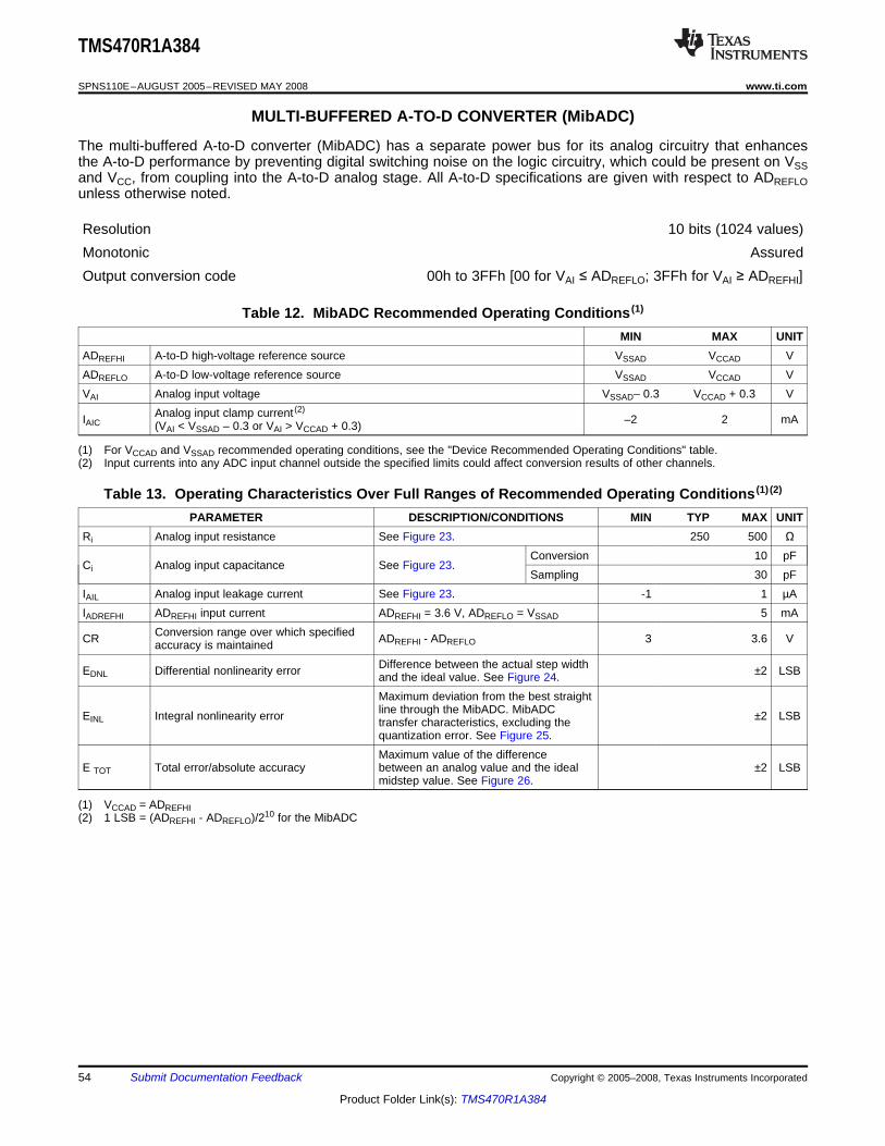
MULTI-BUFFERED A-TO-D CONVERTER (MibADC)
TMS470R1A384
SPNS110E–AUGUST 2005–REVISED MAY 2008 ......................................................................................................................................................... www.ti.com
The multi-buffered A-to-D converter (MibADC) has a separate power bus for its analog circuitry that enhancesthe A-to-D performance by preventing digital switching noise on the logic circuitry, which could be present on VSSand VCC, from coupling into the A-to-D analog stage. All A-to-D specifications are given with respect to ADREFLOunless otherwise noted.
Resolution 10 bits (1024 values)Monotonic AssuredOutput conversion code 00h to 3FFh [00 for VAI ≤ ADREFLO; 3FFh for VAI ≥ ADREFHI]
Table 12. MibADC Recommended Operating Conditions (1)
MIN MAX UNITADREFHI A-to-D high-voltage reference source VSSAD VCCAD VADREFLO A-to-D low-voltage reference source VSSAD VCCAD VVAI Analog input voltage VSSAD– 0.3 VCCAD + 0.3 V
Analog input clamp current (2)IAIC –2 2 mA(VAI < VSSAD – 0.3 or VAI > VCCAD + 0.3)
(1) For VCCAD and VSSAD recommended operating conditions, see the "Device Recommended Operating Conditions" table.(2) Input currents into any ADC input channel outside the specified limits could affect conversion results of other channels.
Table 13. Operating Characteristics Over Full Ranges of Recommended Operating Conditions (1) (2)
PARAMETER DESCRIPTION/CONDITIONS MIN TYP MAX UNITRi Analog input resistance See Figure 23. 250 500 Ω
Conversion 10 pFCi Analog input capacitance See Figure 23.
Sampling 30 pFIAIL Analog input leakage current See Figure 23. -1 1 µAIADREFHI ADREFHI input current ADREFHI = 3.6 V, ADREFLO = VSSAD 5 mA
Conversion range over which specifiedCR ADREFHI - ADREFLO 3 3.6 Vaccuracy is maintainedDifference between the actual step widthEDNL Differential nonlinearity error ±2 LSBand the ideal value. See Figure 24.Maximum deviation from the best straightline through the MibADC. MibADCEINL Integral nonlinearity error ±2 LSBtransfer characteristics, excluding thequantization error. See Figure 25.Maximum value of the difference
E TOT Total error/absolute accuracy between an analog value and the ideal ±2 LSBmidstep value. See Figure 26.
(1) VCCAD = ADREFHI(2) 1 LSB = (ADREFHI - ADREFLO)/210 for the MibADC
54 Submit Documentation Feedback Copyright © 2005–2008, Texas Instruments Incorporated
Product Folder Link(s): TMS470R1A384
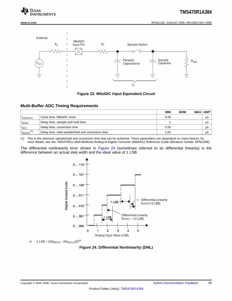
Multi-Buffer ADC Timing Requirements
!
!
TMS470R1A384
www.ti.com ......................................................................................................................................................... SPNS110E–AUGUST 2005–REVISED MAY 2008
Figure 23. MibADC Input Equivalent Circuit
MIN NOM MAX UNITtc(ADCLK) Cycle time, MibADC clock 0.05 µstd(SH) Delay time, sample and hold time 1 µstd(C) Delay time, conversion time 0.55 µstd(SHC)
(1) Delay time, total sample/hold and conversion time 1.55 µs
(1) This is the minimum sample/hold and conversion time that can be achieved. These parameters are dependent on many factors; formore details, see the TMS470R1x Multi-Buffered Analog-to-Digital Converter (MibADC) Reference Guide (literature number SPNU206).
The differential nonlinearity error shown in Figure 24 (sometimes referred to as differential linearity) is thedifference between an actual step width and the ideal value of 1 LSB.
A. 1 LSB = (ADREFHI - ADREFLO)/210
Figure 24. Differential Nonlinearity (DNL)
Copyright © 2005–2008, Texas Instruments Incorporated Submit Documentation Feedback 55
Product Folder Link(s): TMS470R1A384
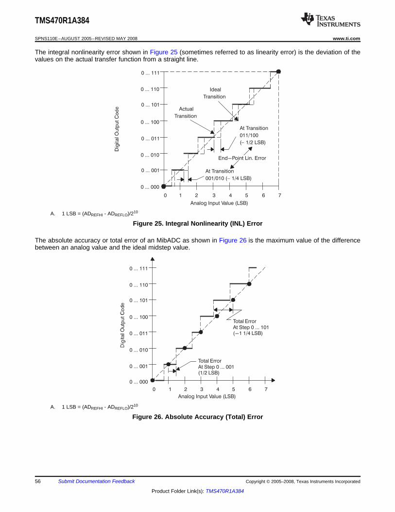
!%$%
$"#$
&
$"" "
$"#$
&
"#$
$%
"#$
TMS470R1A384
SPNS110E–AUGUST 2005–REVISED MAY 2008 ......................................................................................................................................................... www.ti.com
The integral nonlinearity error shown in Figure 25 (sometimes referred to as linearity error) is the deviation of thevalues on the actual transfer function from a straight line.
A. 1 LSB = (ADREFHI - ADREFLO)/210
Figure 25. Integral Nonlinearity (INL) Error
The absolute accuracy or total error of an MibADC as shown in Figure 26 is the maximum value of the differencebetween an analog value and the ideal midstep value.
A. 1 LSB = (ADREFHI - ADREFLO)/210
Figure 26. Absolute Accuracy (Total) Error
56 Submit Documentation Feedback Copyright © 2005–2008, Texas Instruments Incorporated
Product Folder Link(s): TMS470R1A384
PGE Thermal Resistance Characteristics
PZ Thermal Resistance Characteristics
TMS470R1A384
www.ti.com ......................................................................................................................................................... SPNS110E–AUGUST 2005–REVISED MAY 2008
PARAMETER °C/WRθJA 43RθJC 5
PARAMETER °C/WRθJA 48RθJC 5
Copyright © 2005–2008, Texas Instruments Incorporated Submit Documentation Feedback 57
Product Folder Link(s): TMS470R1A384
TMS470R1A384
SPNS110E–AUGUST 2005–REVISED MAY 2008 ......................................................................................................................................................... www.ti.com
Revision HistoryThis revision history highlights the changes made to the device-specific datasheet SPNS110.
Table 14. Revision HistorySPNS110D to SPNS110ECorrected the device-specific part number from 0100001 to 0101101 in Table 10.SPNS110C to SPNS110DRemoved reference to GIOH[5:0] in Terminal Functions table.Changed Output Current for AWD terminal from 8 mA to 4 mA in Terminal Functions table.Changed beginning address for Peripheral Control Registers to 0xFFF0_0000 in Figure 1.Changed register value in Device Identification Code RegisterChanged unit for "VCC digital supply current (standby mode)" from µA to mA in Electrical Characteristics.SPNS110B to SPNS110CRemoved references to digital watchdog (DWD) on page 5.SPNS110A to SPNS110BRevised the Family Nomenclature drawing to add Q version of the temperature range.Revised "Absolute Maximum Ratings" table to add Q version of the temperature range.Revised "Device Recommended Operating Conditions" table to add Q version of the temperature range.Revised "Electrical Characteristics" table to add T and Q temperature versions to ICC specification.Changed T version ICC, standby mode, max to 1. Added Q version ICC standby mode, max of 1.25.Changed T version ICC, halt mode, max to 365. Added Q version ICC halt mode, max of 550.Added note to PORRST Timing Diagram.Changed TA range to –40°C to 125°C on twec in "Timing Requirements for Program Flash" table.Added twec MIN value of 50000 and deleted TYP value in "Timing Requirements for Program Flash" table.Changed terase(sector) TYP value to 1.7 and removed MAX value in "Timing Requirements for Program Flash" table.SPNS110 to SPNS110ACorrected max value for ICC standby and halt modes in Electrical Characteristics table.
58 Submit Documentation Feedback Copyright © 2005–2008, Texas Instruments Incorporated
Product Folder Link(s): TMS470R1A384
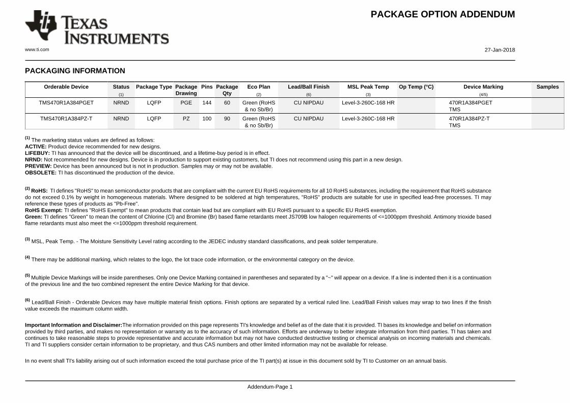
PACKAGE OPTION ADDENDUM
www.ti.com 27-Jan-2018
Addendum-Page 1
PACKAGING INFORMATION
Orderable Device Status(1)
Package Type PackageDrawing
Pins PackageQty
Eco Plan(2)
Lead/Ball Finish(6)
MSL Peak Temp(3)
Op Temp (°C) Device Marking(4/5)
Samples
TMS470R1A384PGET NRND LQFP PGE 144 60 Green (RoHS& no Sb/Br)
CU NIPDAU Level-3-260C-168 HR 470R1A384PGETTMS
TMS470R1A384PZ-T NRND LQFP PZ 100 90 Green (RoHS& no Sb/Br)
CU NIPDAU Level-3-260C-168 HR 470R1A384PZ-TTMS
(1) The marketing status values are defined as follows:ACTIVE: Product device recommended for new designs.LIFEBUY: TI has announced that the device will be discontinued, and a lifetime-buy period is in effect.NRND: Not recommended for new designs. Device is in production to support existing customers, but TI does not recommend using this part in a new design.PREVIEW: Device has been announced but is not in production. Samples may or may not be available.OBSOLETE: TI has discontinued the production of the device.
(2) RoHS: TI defines "RoHS" to mean semiconductor products that are compliant with the current EU RoHS requirements for all 10 RoHS substances, including the requirement that RoHS substancedo not exceed 0.1% by weight in homogeneous materials. Where designed to be soldered at high temperatures, "RoHS" products are suitable for use in specified lead-free processes. TI mayreference these types of products as "Pb-Free".RoHS Exempt: TI defines "RoHS Exempt" to mean products that contain lead but are compliant with EU RoHS pursuant to a specific EU RoHS exemption.Green: TI defines "Green" to mean the content of Chlorine (Cl) and Bromine (Br) based flame retardants meet JS709B low halogen requirements of <=1000ppm threshold. Antimony trioxide basedflame retardants must also meet the <=1000ppm threshold requirement.
(3) MSL, Peak Temp. - The Moisture Sensitivity Level rating according to the JEDEC industry standard classifications, and peak solder temperature.
(4) There may be additional marking, which relates to the logo, the lot trace code information, or the environmental category on the device.
(5) Multiple Device Markings will be inside parentheses. Only one Device Marking contained in parentheses and separated by a "~" will appear on a device. If a line is indented then it is a continuationof the previous line and the two combined represent the entire Device Marking for that device.
(6) Lead/Ball Finish - Orderable Devices may have multiple material finish options. Finish options are separated by a vertical ruled line. Lead/Ball Finish values may wrap to two lines if the finishvalue exceeds the maximum column width.
Important Information and Disclaimer:The information provided on this page represents TI's knowledge and belief as of the date that it is provided. TI bases its knowledge and belief on informationprovided by third parties, and makes no representation or warranty as to the accuracy of such information. Efforts are underway to better integrate information from third parties. TI has taken andcontinues to take reasonable steps to provide representative and accurate information but may not have conducted destructive testing or chemical analysis on incoming materials and chemicals.TI and TI suppliers consider certain information to be proprietary, and thus CAS numbers and other limited information may not be available for release.
In no event shall TI's liability arising out of such information exceed the total purchase price of the TI part(s) at issue in this document sold by TI to Customer on an annual basis.
PACKAGE OPTION ADDENDUM
www.ti.com 27-Jan-2018
Addendum-Page 2
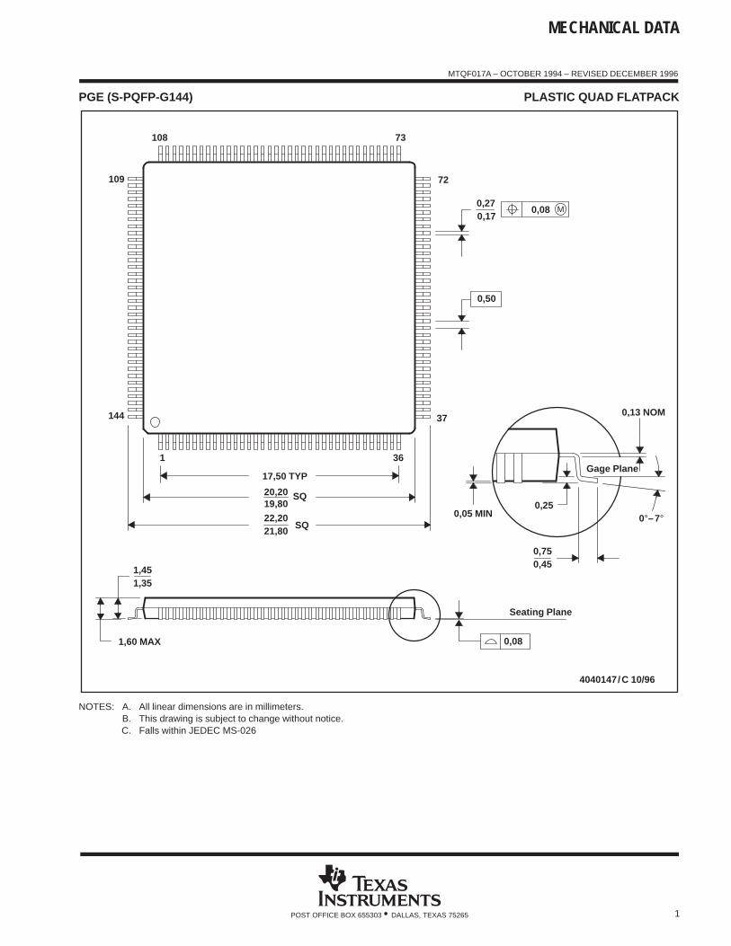
MECHANICAL DATA
MTQF017A – OCTOBER 1994 – REVISED DECEMBER 1996
1POST OFFICE BOX 655303 • DALLAS, TEXAS 75265
PGE (S-PQFP-G144) PLASTIC QUAD FLATPACK
4040147/C 10/96
0,27
72
0,17
37
73
0,13 NOM
0,25
0,750,45
0,05 MIN
36
Seating Plane
Gage Plane
108
109
144
SQ
SQ22,2021,80
1
19,80
17,50 TYP
20,20
1,351,45
1,60 MAX
M0,08
0°–7°
0,08
0,50
NOTES: A. All linear dimensions are in millimeters.B. This drawing is subject to change without notice.C. Falls within JEDEC MS-026
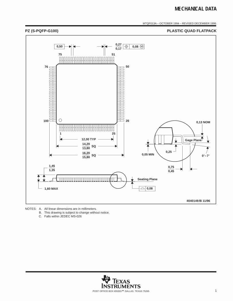
MECHANICAL DATA
MTQF013A – OCTOBER 1994 – REVISED DECEMBER 1996
1POST OFFICE BOX 655303 • DALLAS, TEXAS 75265
PZ (S-PQFP-G100) PLASTIC QUAD FLATPACK
4040149/B 11/96
50
26 0,13 NOM
Gage Plane
0,25
0,450,75
0,05 MIN
0,27
51
25
75
1
12,00 TYP
0,17
76
100
SQ
SQ15,8016,20
13,80
1,351,45
1,60 MAX
14,20
0°–7°
Seating Plane
0,08
0,50 M0,08
NOTES: A. All linear dimensions are in millimeters.B. This drawing is subject to change without notice.C. Falls within JEDEC MS-026
IMPORTANT NOTICE
Texas Instruments Incorporated (TI) reserves the right to make corrections, enhancements, improvements and other changes to itssemiconductor products and services per JESD46, latest issue, and to discontinue any product or service per JESD48, latest issue. Buyersshould obtain the latest relevant information before placing orders and should verify that such information is current and complete.TI’s published terms of sale for semiconductor products (http://www.ti.com/sc/docs/stdterms.htm) apply to the sale of packaged integratedcircuit products that TI has qualified and released to market. Additional terms may apply to the use or sale of other types of TI products andservices.Reproduction of significant portions of TI information in TI data sheets is permissible only if reproduction is without alteration and isaccompanied by all associated warranties, conditions, limitations, and notices. TI is not responsible or liable for such reproduceddocumentation. Information of third parties may be subject to additional restrictions. Resale of TI products or services with statementsdifferent from or beyond the parameters stated by TI for that product or service voids all express and any implied warranties for theassociated TI product or service and is an unfair and deceptive business practice. TI is not responsible or liable for any such statements.Buyers and others who are developing systems that incorporate TI products (collectively, “Designers”) understand and agree that Designersremain responsible for using their independent analysis, evaluation and judgment in designing their applications and that Designers havefull and exclusive responsibility to assure the safety of Designers' applications and compliance of their applications (and of all TI productsused in or for Designers’ applications) with all applicable regulations, laws and other applicable requirements. Designer represents that, withrespect to their applications, Designer has all the necessary expertise to create and implement safeguards that (1) anticipate dangerousconsequences of failures, (2) monitor failures and their consequences, and (3) lessen the likelihood of failures that might cause harm andtake appropriate actions. Designer agrees that prior to using or distributing any applications that include TI products, Designer willthoroughly test such applications and the functionality of such TI products as used in such applications.TI’s provision of technical, application or other design advice, quality characterization, reliability data or other services or information,including, but not limited to, reference designs and materials relating to evaluation modules, (collectively, “TI Resources”) are intended toassist designers who are developing applications that incorporate TI products; by downloading, accessing or using TI Resources in anyway, Designer (individually or, if Designer is acting on behalf of a company, Designer’s company) agrees to use any particular TI Resourcesolely for this purpose and subject to the terms of this Notice.TI’s provision of TI Resources does not expand or otherwise alter TI’s applicable published warranties or warranty disclaimers for TIproducts, and no additional obligations or liabilities arise from TI providing such TI Resources. TI reserves the right to make corrections,enhancements, improvements and other changes to its TI Resources. TI has not conducted any testing other than that specificallydescribed in the published documentation for a particular TI Resource.Designer is authorized to use, copy and modify any individual TI Resource only in connection with the development of applications thatinclude the TI product(s) identified in such TI Resource. NO OTHER LICENSE, EXPRESS OR IMPLIED, BY ESTOPPEL OR OTHERWISETO ANY OTHER TI INTELLECTUAL PROPERTY RIGHT, AND NO LICENSE TO ANY TECHNOLOGY OR INTELLECTUAL PROPERTYRIGHT OF TI OR ANY THIRD PARTY IS GRANTED HEREIN, including but not limited to any patent right, copyright, mask work right, orother intellectual property right relating to any combination, machine, or process in which TI products or services are used. Informationregarding or referencing third-party products or services does not constitute a license to use such products or services, or a warranty orendorsement thereof. Use of TI Resources may require a license from a third party under the patents or other intellectual property of thethird party, or a license from TI under the patents or other intellectual property of TI.TI RESOURCES ARE PROVIDED “AS IS” AND WITH ALL FAULTS. TI DISCLAIMS ALL OTHER WARRANTIES ORREPRESENTATIONS, EXPRESS OR IMPLIED, REGARDING RESOURCES OR USE THEREOF, INCLUDING BUT NOT LIMITED TOACCURACY OR COMPLETENESS, TITLE, ANY EPIDEMIC FAILURE WARRANTY AND ANY IMPLIED WARRANTIES OFMERCHANTABILITY, FITNESS FOR A PARTICULAR PURPOSE, AND NON-INFRINGEMENT OF ANY THIRD PARTY INTELLECTUALPROPERTY RIGHTS. TI SHALL NOT BE LIABLE FOR AND SHALL NOT DEFEND OR INDEMNIFY DESIGNER AGAINST ANY CLAIM,INCLUDING BUT NOT LIMITED TO ANY INFRINGEMENT CLAIM THAT RELATES TO OR IS BASED ON ANY COMBINATION OFPRODUCTS EVEN IF DESCRIBED IN TI RESOURCES OR OTHERWISE. IN NO EVENT SHALL TI BE LIABLE FOR ANY ACTUAL,DIRECT, SPECIAL, COLLATERAL, INDIRECT, PUNITIVE, INCIDENTAL, CONSEQUENTIAL OR EXEMPLARY DAMAGES INCONNECTION WITH OR ARISING OUT OF TI RESOURCES OR USE THEREOF, AND REGARDLESS OF WHETHER TI HAS BEENADVISED OF THE POSSIBILITY OF SUCH DAMAGES.Unless TI has explicitly designated an individual product as meeting the requirements of a particular industry standard (e.g., ISO/TS 16949and ISO 26262), TI is not responsible for any failure to meet such industry standard requirements.Where TI specifically promotes products as facilitating functional safety or as compliant with industry functional safety standards, suchproducts are intended to help enable customers to design and create their own applications that meet applicable functional safety standardsand requirements. Using products in an application does not by itself establish any safety features in the application. Designers mustensure compliance with safety-related requirements and standards applicable to their applications. Designer may not use any TI products inlife-critical medical equipment unless authorized officers of the parties have executed a special contract specifically governing such use.Life-critical medical equipment is medical equipment where failure of such equipment would cause serious bodily injury or death (e.g., lifesupport, pacemakers, defibrillators, heart pumps, neurostimulators, and implantables). Such equipment includes, without limitation, allmedical devices identified by the U.S. Food and Drug Administration as Class III devices and equivalent classifications outside the U.S.TI may expressly designate certain products as completing a particular qualification (e.g., Q100, Military Grade, or Enhanced Product).Designers agree that it has the necessary expertise to select the product with the appropriate qualification designation for their applicationsand that proper product selection is at Designers’ own risk. Designers are solely responsible for compliance with all legal and regulatoryrequirements in connection with such selection.Designer will fully indemnify TI and its representatives against any damages, costs, losses, and/or liabilities arising out of Designer’s non-compliance with the terms and provisions of this Notice.
Mailing Address: Texas Instruments, Post Office Box 655303, Dallas, Texas 75265Copyright © 2018, Texas Instruments Incorporated
Related Documents


