©2006 Silicon Storage Technology, Inc. S71271-02-000 1/06 1 The SST logo and SuperFlash are registered Trademarks of Silicon Storage Technology, Inc. These specifications are subject to change without notice. Data Sheet FEATURES: • Single Voltage Read and Write Operations – 2.7-3.6V • Serial Interface Architecture – SPI Compatible: Mode 0 and Mode 3 • High Speed Clock Frequency – 50 MHz • Superior Reliability – Endurance: 100,000 Cycles (typical) – Greater than 100 years Data Retention • Low Power Consumption: – Active Read Current: 10 mA (typical) – Standby Current: 5 μA (typical) • Flexible Erase Capability – Uniform 4 KByte sectors – Uniform 32 KByte overlay blocks – Uniform 64 KByte overlay blocks • Fast Erase and Byte-Program: – Chip-Erase Time: 35 ms (typical) – Sector-/Block-Erase Time: 18 ms (typical) – Byte-Program Time: 7 μs (typical) • Auto Address Increment (AAI) Programming – Decrease total chip programming time over Byte-Program operations • End-of-Write Detection – Software polling the BUSY bit in Status Register – Busy Status readout on SO pin in AAI Mode • Hold Pin (HOLD#) – Suspends a serial sequence to the memory without deselecting the device • Write Protection (WP#) – Enables/Disables the Lock-Down function of the status register • Software Write Protection – Write protection through Block-Protection bits in status register • Temperature Range – Commercial: 0°C to +70°C – Industrial: -40°C to +85°C • Packages Available – 8-lead SOIC (200 mils) – 8-contact WSON (6mm x 5mm) • All non-Pb (lead-free) devices are RoHS compliant PRODUCT DESCRIPTION SST’s 25 series Serial Flash family features a four-wire, SPI-compatible interface that allows for a low pin-count package which occupies less board space and ultimately lowers total system costs. The SST25VF016B devices are enhanced with improved operating frequency and even lower power consumption than the original SST25VFxxxA devices. SST25VF016B SPI serial flash memories are manufactured with SST’s proprietary, high-performance CMOS SuperFlash technology. The split-gate cell design and thick-oxide tunneling injector attain better reliability and manufacturability compared with alternate approaches. The SST25VF016B devices significantly improve perfor- mance and reliability, while lowering power consumption. The devices write (Program or Erase) with a single power supply of 2.7-3.6V for SST25VF016B. The total energy consumed is a function of the applied voltage, current, and time of application. Since for any given voltage range, the SuperFlash technology uses less current to program and has a shorter erase time, the total energy consumed during any Erase or Program operation is less than alternative flash memory technologies. The SST25VF016B device is offered in both 8-lead SOIC (200 mils) and 8-contact WSON (6mm x 5mm) packages. See Figure 1 for pin assignments. 16 Mbit SPI Serial Flash SST25VF016B SST25VF016B16Mb Serial Peripheral Interface (SPI) flash memory

Welcome message from author
This document is posted to help you gain knowledge. Please leave a comment to let me know what you think about it! Share it to your friends and learn new things together.
Transcript
©2006 Silicon Storage Technology, Inc.S71271-02-000 1/061
The SST logo and SuperFlash are registered Trademarks of Silicon Storage Technology, Inc.These specifications are subject to change without notice.
Data Sheet
FEATURES:
• Single Voltage Read and Write Operations– 2.7-3.6V
• Serial Interface Architecture– SPI Compatible: Mode 0 and Mode 3
• High Speed Clock Frequency– 50 MHz
• Superior Reliability– Endurance: 100,000 Cycles (typical)– Greater than 100 years Data Retention
• Low Power Consumption:– Active Read Current: 10 mA (typical)– Standby Current: 5 µA (typical)
• Flexible Erase Capability– Uniform 4 KByte sectors– Uniform 32 KByte overlay blocks– Uniform 64 KByte overlay blocks
• Fast Erase and Byte-Program:– Chip-Erase Time: 35 ms (typical)– Sector-/Block-Erase Time: 18 ms (typical)– Byte-Program Time: 7 µs (typical)
• Auto Address Increment (AAI) Programming– Decrease total chip programming time over
Byte-Program operations• End-of-Write Detection
– Software polling the BUSY bit in Status Register– Busy Status readout on SO pin in AAI Mode
• Hold Pin (HOLD#)– Suspends a serial sequence to the memory
without deselecting the device• Write Protection (WP#)
– Enables/Disables the Lock-Down function of the status register
• Software Write Protection– Write protection through Block-Protection bits in
status register• Temperature Range
– Commercial: 0°C to +70°C– Industrial: -40°C to +85°C
• Packages Available– 8-lead SOIC (200 mils)– 8-contact WSON (6mm x 5mm)
• All non-Pb (lead-free) devices are RoHS compliant
PRODUCT DESCRIPTION
SST’s 25 series Serial Flash family features a four-wire,SPI-compatible interface that allows for a low pin-countpackage which occupies less board space and ultimatelylowers total system costs. The SST25VF016B devices areenhanced with improved operating frequency and evenlower power consumption than the original SST25VFxxxAdevices. SST25VF016B SPI serial flash memories aremanufactured with SST’s proprietary, high-performanceCMOS SuperFlash technology. The split-gate cell designand thick-oxide tunneling injector attain better reliability andmanufacturability compared with alternate approaches.
The SST25VF016B devices significantly improve perfor-mance and reliability, while lowering power consumption.The devices write (Program or Erase) with a single powersupply of 2.7-3.6V for SST25VF016B. The total energyconsumed is a function of the applied voltage, current, andtime of application. Since for any given voltage range, theSuperFlash technology uses less current to program andhas a shorter erase time, the total energy consumed duringany Erase or Program operation is less than alternativeflash memory technologies.
The SST25VF016B device is offered in both 8-lead SOIC(200 mils) and 8-contact WSON (6mm x 5mm) packages.See Figure 1 for pin assignments.
16 Mbit SPI Serial FlashSST25VF016B
SST25VF016B16Mb Serial Peripheral Interface (SPI) flash memory
2
Data Sheet
16 Mbit SPI Serial FlashSST25VF016B
©2006 Silicon Storage Technology, Inc. S71271-02-000 1/06
1271 B1.0
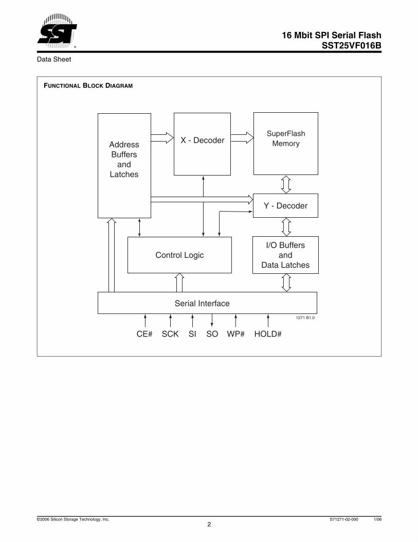
I/O Buffersand
Data Latches
SuperFlashMemoryX - Decoder
Control Logic
AddressBuffers
andLatches
CE#
Y - Decoder
SCK SI SO WP# HOLD#
Serial Interface
FUNCTIONAL BLOCK DIAGRAM
Data Sheet
16 Mbit SPI Serial FlashSST25VF016B
3©2006 Silicon Storage Technology, Inc. S71271-02-000 1/06
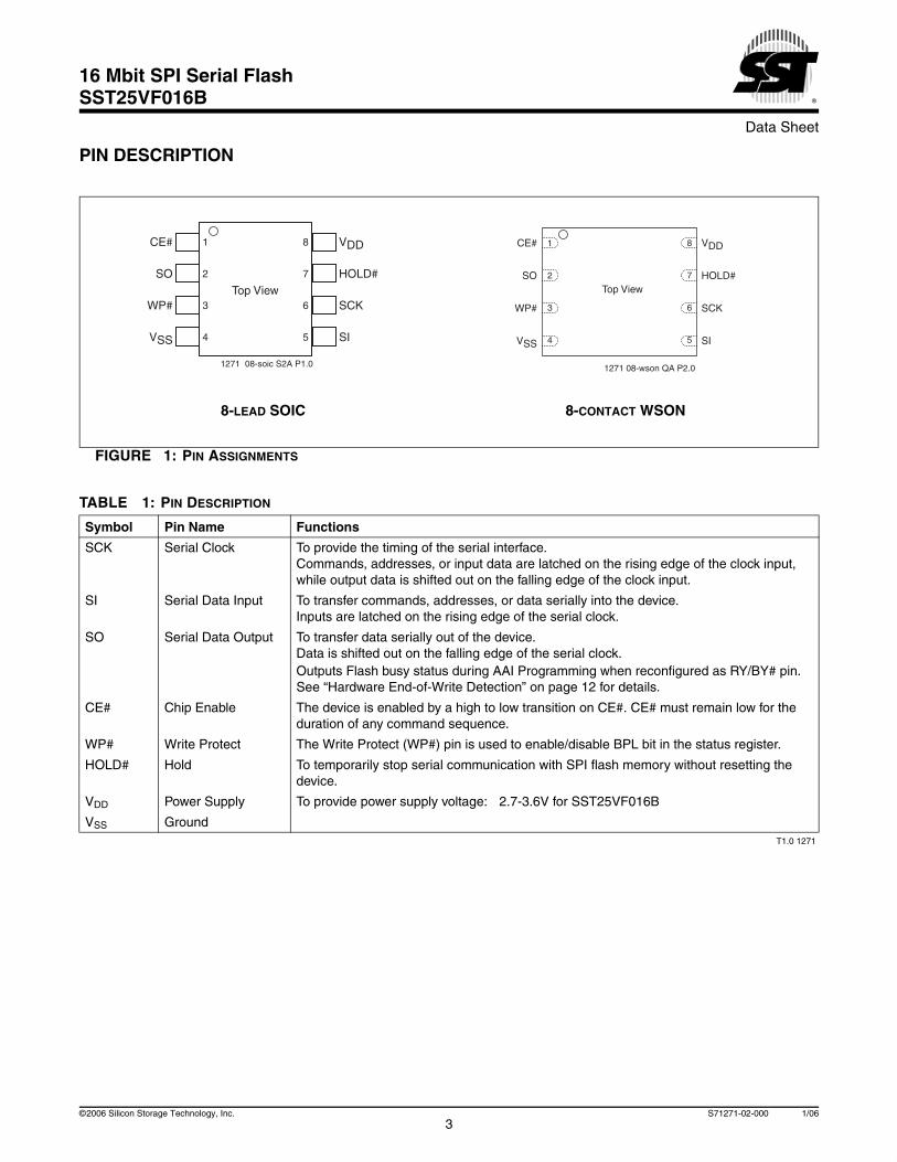
PIN DESCRIPTION
FIGURE 1: PIN ASSIGNMENTS
TABLE 1: PIN DESCRIPTION
Symbol Pin Name Functions
SCK Serial Clock To provide the timing of the serial interface.Commands, addresses, or input data are latched on the rising edge of the clock input, while output data is shifted out on the falling edge of the clock input.
SI Serial Data Input To transfer commands, addresses, or data serially into the device.Inputs are latched on the rising edge of the serial clock.
SO Serial Data Output To transfer data serially out of the device.Data is shifted out on the falling edge of the serial clock.Outputs Flash busy status during AAI Programming when reconfigured as RY/BY# pin. See “Hardware End-of-Write Detection” on page 12 for details.
CE# Chip Enable The device is enabled by a high to low transition on CE#. CE# must remain low for the duration of any command sequence.
WP# Write Protect The Write Protect (WP#) pin is used to enable/disable BPL bit in the status register.
HOLD# Hold To temporarily stop serial communication with SPI flash memory without resetting the device.
VDD Power Supply To provide power supply voltage: 2.7-3.6V for SST25VF016B
VSS GroundT1.0 1271
1
2
3
4
8
7
6
5
CE#
SO
WP#
VSS
VDD
HOLD#
SCK
SI
Top View
1271 08-soic S2A P1.0
1
2
3
4
8
7
6
5
CE#
SO
WP#
VSS
Top View
VDD
HOLD#
SCK
SI
1271 08-wson QA P2.0
8-LEAD SOIC 8-CONTACT WSON

4
Data Sheet
16 Mbit SPI Serial FlashSST25VF016B
©2006 Silicon Storage Technology, Inc. S71271-02-000 1/06
MEMORY ORGANIZATION
The SST25VF016B SuperFlash memory array is orga-nized in uniform 4 KByte erasable sectors with 32 KByteoverlay blocks and 64 KByte overlay erasable blocks.
DEVICE OPERATION
The SST25VF016B is accessed through the SPI (SerialPeripheral Interface) bus compatible protocol. The SPI busconsist of four control lines; Chip Enable (CE#) is used to
select the device, and data is accessed through the SerialData Input (SI), Serial Data Output (SO), and Serial Clock(SCK).
The SST25VF016B supports both Mode 0 (0,0) and Mode3 (1,1) of SPI bus operations. The difference between thetwo modes, as shown in Figure 2, is the state of the SCKsignal when the bus master is in Stand-by mode and nodata is being transferred. The SCK signal is low for Mode 0and SCK signal is high for Mode 3. For both modes, theSerial Data In (SI) is sampled at the rising edge of the SCKclock signal and the Serial Data Output (SO) is driven afterthe falling edge of the SCK clock signal.
FIGURE 2: SPI PROTOCOL
1271 SPIprot.0
MODE 3
SCK
SI
SO
CE#MODE 3
DON'T CARE
Bit 7 Bit 6 Bit 5 Bit 4 Bit 3 Bit 2 Bit 1 Bit 0
Bit 7 Bit 6 Bit 5 Bit 4 Bit 3 Bit 2 Bit 1 Bit 0
MODE 0MODE 0
HIGH IMPEDANCEMSB
MSB

Data Sheet
16 Mbit SPI Serial FlashSST25VF016B
5©2006 Silicon Storage Technology, Inc. S71271-02-000 1/06
Hold OperationThe HOLD# pin is used to pause a serial sequence under-way with the SPI flash memory without resetting the clock-ing sequence. To activate the HOLD# mode, CE# must bein active low state. The HOLD# mode begins when theSCK active low state coincides with the falling edge of theHOLD# signal. The HOLD mode ends when the HOLD#signal’s rising edge coincides with the SCK active low state.
If the falling edge of the HOLD# signal does not coincidewith the SCK active low state, then the device enters Holdmode when the SCK next reaches the active low state.Similarly, if the rising edge of the HOLD# signal does not
coincide with the SCK active low state, then the deviceexits in Hold mode when the SCK next reaches the activelow state. See Figure 3 for Hold Condition waveform.
Once the device enters Hold mode, SO will be in high-impedance state while SI and SCK can be VIL or VIH.
If CE# is driven active high during a Hold condition, it resetsthe internal logic of the device. As long as HOLD# signal islow, the memory remains in the Hold condition. To resumecommunication with the device, HOLD# must be drivenactive high, and CE# must be driven active low. See Figure23 for Hold timing.
FIGURE 3: HOLD CONDITION WAVEFORM
Write ProtectionSST25VF016B provides software Write protection. TheWrite Protect pin (WP#) enables or disables the lock-downfunction of the status register. The Block-Protection bits(BP3, BP2, BP1, BP0, and BPL) in the status register pro-vide Write protection to the memory array and the statusregister. See Table 4 for the Block-Protection description.
Write Protect Pin (WP#)
The Write Protect (WP#) pin enables the lock-down func-tion of the BPL bit (bit 7) in the status register. When WP#is driven low, the execution of the Write-Status-Register(WRSR) instruction is determined by the value of the BPLbit (see Table 2). When WP# is high, the lock-down func-tion of the BPL bit is disabled.
Active Hold Active Hold Active
1271 HoldCond.0
SCK
HOLD#
TABLE 2: CONDITIONS TO EXECUTE WRITE-STATUS-REGISTER (WRSR) INSTRUCTION
WP# BPL Execute WRSR Instruction
L 1 Not Allowed
L 0 Allowed
H X AllowedT2.0 1271
6
Data Sheet
16 Mbit SPI Serial FlashSST25VF016B
©2006 Silicon Storage Technology, Inc. S71271-02-000 1/06
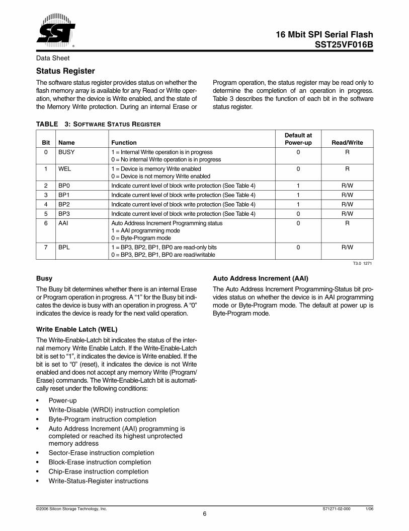
Status RegisterThe software status register provides status on whether theflash memory array is available for any Read or Write oper-ation, whether the device is Write enabled, and the state ofthe Memory Write protection. During an internal Erase or
Program operation, the status register may be read only todetermine the completion of an operation in progress.Table 3 describes the function of each bit in the softwarestatus register.
Busy
The Busy bit determines whether there is an internal Eraseor Program operation in progress. A “1” for the Busy bit indi-cates the device is busy with an operation in progress. A “0”indicates the device is ready for the next valid operation.
Write Enable Latch (WEL)
The Write-Enable-Latch bit indicates the status of the inter-nal memory Write Enable Latch. If the Write-Enable-Latchbit is set to “1”, it indicates the device is Write enabled. If thebit is set to “0” (reset), it indicates the device is not Writeenabled and does not accept any memory Write (Program/Erase) commands. The Write-Enable-Latch bit is automati-cally reset under the following conditions:
• Power-up• Write-Disable (WRDI) instruction completion• Byte-Program instruction completion• Auto Address Increment (AAI) programming is
completed or reached its highest unprotected memory address
• Sector-Erase instruction completion• Block-Erase instruction completion• Chip-Erase instruction completion• Write-Status-Register instructions
Auto Address Increment (AAI)
The Auto Address Increment Programming-Status bit pro-vides status on whether the device is in AAI programmingmode or Byte-Program mode. The default at power up isByte-Program mode.
TABLE 3: SOFTWARE STATUS REGISTER
Bit Name FunctionDefault atPower-up Read/Write
0 BUSY 1 = Internal Write operation is in progress0 = No internal Write operation is in progress
0 R
1 WEL 1 = Device is memory Write enabled0 = Device is not memory Write enabled
0 R
2 BP0 Indicate current level of block write protection (See Table 4) 1 R/W
3 BP1 Indicate current level of block write protection (See Table 4) 1 R/W
4 BP2 Indicate current level of block write protection (See Table 4) 1 R/W
5 BP3 Indicate current level of block write protection (See Table 4) 0 R/W
6 AAI Auto Address Increment Programming status1 = AAI programming mode0 = Byte-Program mode
0 R
7 BPL 1 = BP3, BP2, BP1, BP0 are read-only bits0 = BP3, BP2, BP1, BP0 are read/writable
0 R/W
T3.0 1271

Data Sheet
16 Mbit SPI Serial FlashSST25VF016B
7©2006 Silicon Storage Technology, Inc. S71271-02-000 1/06
Block Protection (BP3,BP2, BP1, BP0)
The Block-Protection (BP3, BP2, BP1, BP0) bits define thesize of the memory area, as defined in Table 4, to be soft-ware protected against any memory Write (Program orErase) operation. The Write-Status-Register (WRSR)instruction is used to program the BP3, BP2, BP1 and BP0bits as long as WP# is high or the Block-Protect-Lock(BPL) bit is 0. Chip-Erase can only be executed if Block-Protection bits are all 0. After power-up, BP3, BP2, BP1and BP0 are set to 1.
Block Protection Lock-Down (BPL)
WP# pin driven low (VIL), enables the Block-Protection-Lock-Down (BPL) bit. When BPL is set to 1, it prevents anyfurther alteration of the BPL, BP3, BP2, BP1, and BP0 bits.When the WP# pin is driven high (VIH), the BPL bit has noeffect and its value is “Don’t Care”. After power-up, the BPLbit is reset to 0.
TABLE 4: SOFTWARE STATUS REGISTER BLOCK PROTECTION FOR SST25VF016B1
1. X = Don’t Care (RESERVED) default is “0
Protection Level
Status Register Bit2
2. Default at power-up for BP2, BP1, and BP0 is ‘111’. (All Blocks Protected)
Protected Memory Address
BP3 BP2 BP1 BP0 16 Mbit
None X 0 0 0 None
Upper 1/32 X 0 0 1 1F0000H-1FFFFFH
Upper 1/16 X 0 1 0 1E0000H-1FFFFFH
Upper 1/8 X 0 1 1 1C0000H-1FFFFFH
Upper 1/4 X 1 0 0 180000H-1FFFFFH
Upper 1/2 X 1 0 1 100000H-1FFFFFH
All Blocks X 1 1 0 000000H-1FFFFFH
All Blocks X 1 1 1 000000H-1FFFFFHT4.0 1271

8
Data Sheet
16 Mbit SPI Serial FlashSST25VF016B
©2006 Silicon Storage Technology, Inc. S71271-02-000 1/06
InstructionsInstructions are used to read, write (Erase and Program),and configure the SST25VF016B. The instruction buscycles are 8 bits each for commands (Op Code), data, andaddresses. Prior to executing any Byte-Program, AutoAddress Increment (AAI) programming, Sector-Erase,Block-Erase, Write-Status-Register, or Chip-Erase instruc-tions, the Write-Enable (WREN) instruction must be exe-cuted first. The complete list of instructions is provided inTable 5. All instructions are synchronized off a high to lowtransition of CE#. Inputs will be accepted on the rising edge
of SCK starting with the most significant bit. CE# must bedriven low before an instruction is entered and must bedriven high after the last bit of the instruction has beenshifted in (except for Read, Read-ID, and Read-Status-Register instructions). Any low to high transition on CE#,before receiving the last bit of an instruction bus cycle, willterminate the instruction in progress and return the deviceto standby mode. Instruction commands (Op Code),addresses, and data are all input from the most significantbit (MSB) first.
TABLE 5: DEVICE OPERATION INSTRUCTIONS
Instruction Description Op Code Cycle1
1. One bus cycle is eight clock periods.
Address Cycle(s)2
2. Address bits above the most significant bit of each density can be VIL or VIH.
Dummy Cycle(s)
DataCycle(s)
Maximum Frequency
Read Read Memory at 25 MHz 0000 0011b (03H) 3 0 1 to ∞ 25 MHz
High-Speed Read Read Memory at 50 MHz 0000 1011b (0BH) 3 1 1 to ∞ 50 MHz
4 KByte Sector-Erase3
3. 4KByte Sector Erase addresses: use AMS-A12, remaining addresses are don’t care but must be set either at VIL or VIH.
Erase 4 KByte of memory array
0010 0000b (20H) 3 0 0 50 MHz
32 KByte Block-Erase4
4. 32KByte Block Erase addresses: use AMS-A15, remaining addresses are don’t care but must be set either at VIL or VIH.
Erase 32 KByte block of memory array
0101 0010b (52H) 3 0 0 50 MHz
64 KByte Block-Erase5
5. 64KByte Block Erase addresses: use AMS-A16, remaining addresses are don’t care but must be set either at VIL or VIH.
Erase 64 KByte block of memory array
1101 1000b (D8H) 3 0 0 50 MHz
Chip-Erase Erase Full Memory Array 0110 0000b (60H) or 1100 0111b (C7H)
0 0 0 50 MHz
Byte-Program To Program One Data Byte 0000 0010b (02H) 3 0 1 50 MHz
AAI-Word-Program6
6. To continue programming to the next sequential address location, enter the 8-bit command, ADH, followed by 2 bytes of data to be programmed. Data Byte 0 will be programmed into the initial address [A23-A1] with A0=0, Data Byte 1 will be programmed into the initial address [A23-A1] with A0=1.
Auto Address Increment Programming
1010 1101b (ADH) 3 0 2 to ∞ 50 MHz
RDSR7
7. The Read-Status-Register is continuous with ongoing clock cycles until terminated by a low to high transition on CE#.
Read-Status-Register 0000 0101b (05H) 0 0 1 to ∞ 50 MHz
EWSR Enable-Write-Status-Register 0101b 0000b (50H) 0 0 0 50 MHz
WRSR Write-Status-Register 0000 0001b (01H) 0 0 1 50 MHz
WREN Write-Enable 0000 0110b (06H) 0 0 0 50 MHz
WRDI Write-Disable 0000 0100b (04H) 0 0 0 50 MHz
RDID8
8. Manufacturer’s ID is read with A0=0, and Device ID is read with A0=1. All other address bits are 00H. The Manufacturer’s ID and device ID output stream is continuous until terminated by a low-to-high transition on CE#.
Read-ID 1001 0000b (90H) or 1010 1011b (ABH)
3 0 1 to ∞ 50 MHz
JEDEC-ID JEDEC ID read 1001 1111b (9FH) 0 0 3 to ∞ 50 MHz
EBSY Enable SO to output RY/BY# status during AAI programming
0111 0000b (70H) 0 0 0 50 MHz
DBSY Disable SO to output RY/BY# status during AAI programming
1000 0000b (80H) 0 0 0 50 MHz
T5.0 1271

Data Sheet
16 Mbit SPI Serial FlashSST25VF016B
9©2006 Silicon Storage Technology, Inc. S71271-02-000 1/06
Read (25 MHz)
The Read instruction, 03H, supports up to 25 MHz Read.The device outputs the data starting from the specifiedaddress location. The data output stream is continuousthrough all addresses until terminated by a low to high tran-sition on CE#. The internal address pointer will automati-cally increment until the highest memory address isreached. Once the highest memory address is reached,the address pointer will automatically increment to the
beginning (wrap-around) of the address space. Once thedata from address location 1FFFFFH has been read, thenext output will be from address location 000000H.
The Read instruction is initiated by executing an 8-bit com-mand, 03H, followed by address bits [A23-A0]. CE# mustremain active low for the duration of the Read cycle. SeeFigure 4 for the Read sequence.
FIGURE 4: READ SEQUENCE
1271 ReadSeq.0
CE#
SO
SI
SCK
ADD.
0 1 2 3 4 5 6 7 8
ADD. ADD.03
HIGH IMPEDANCE
15 16 23 24 31 32 39 40 7047 48 55 56 63 64
N+2 N+3 N+4N N+1DOUT
MSB MSB
MSB
MODE 0
MODE 3
DOUT DOUT DOUT DOUT
10
Data Sheet
16 Mbit SPI Serial FlashSST25VF016B
©2006 Silicon Storage Technology, Inc. S71271-02-000 1/06
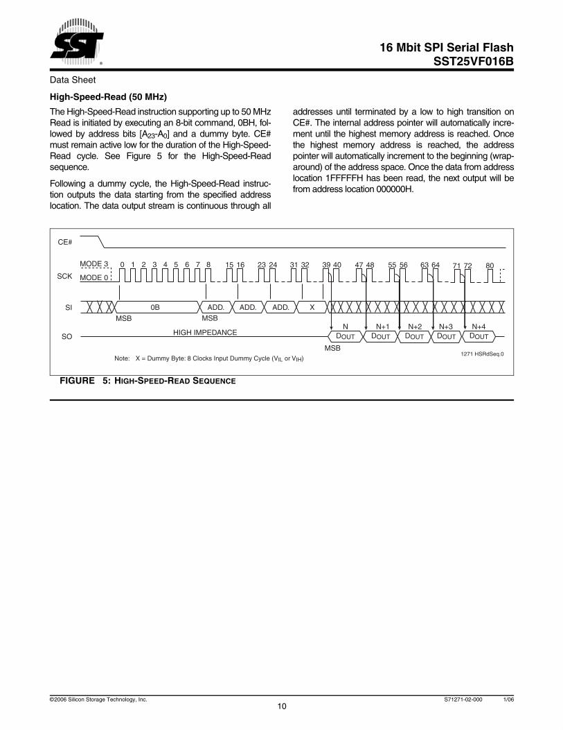
High-Speed-Read (50 MHz)
The High-Speed-Read instruction supporting up to 50 MHzRead is initiated by executing an 8-bit command, 0BH, fol-lowed by address bits [A23-A0] and a dummy byte. CE#must remain active low for the duration of the High-Speed-Read cycle. See Figure 5 for the High-Speed-Readsequence.
Following a dummy cycle, the High-Speed-Read instruc-tion outputs the data starting from the specified addresslocation. The data output stream is continuous through all
addresses until terminated by a low to high transition onCE#. The internal address pointer will automatically incre-ment until the highest memory address is reached. Oncethe highest memory address is reached, the addresspointer will automatically increment to the beginning (wrap-around) of the address space. Once the data from addresslocation 1FFFFFH has been read, the next output will befrom address location 000000H.
FIGURE 5: HIGH-SPEED-READ SEQUENCE
1271 HSRdSeq.0
CE#
SO
SI
SCK
ADD.
0 1 2 3 4 5 6 7 8
ADD. ADD.0B
HIGH IMPEDANCE
15 16 23 24 31 32 39 40 47 48 55 56 63 64
N+2 N+3 N+4N N+1
X
MSB
MSBMSB
MODE 0
MODE 3
DOUT DOUT DOUT DOUT
8071 72
DOUT
Note: X = Dummy Byte: 8 Clocks Input Dummy Cycle (VIL or VIH)

Data Sheet
16 Mbit SPI Serial FlashSST25VF016B
11©2006 Silicon Storage Technology, Inc. S71271-02-000 1/06
Byte-Program
The Byte-Program instruction programs the bits in theselected byte to the desired data. The selected byte mustbe in the erased state (FFH) when initiating a Programoperation. A Byte-Program instruction applied to a pro-tected memory area will be ignored.
Prior to any Write operation, the Write-Enable (WREN)instruction must be executed. CE# must remain active lowfor the duration of the Byte-Program instruction. The Byte-
Program instruction is initiated by executing an 8-bit com-mand, 02H, followed by address bits [A23-A0]. Following theaddress, the data is input in order from MSB (bit 7) to LSB(bit 0). CE# must be driven high before the instruction isexecuted. The user may poll the Busy bit in the softwarestatus register or wait TBP for the completion of the internalself-timed Byte-Program operation. See Figure 6 for theByte-Program sequence.
FIGURE 6: BYTE-PROGRAM SEQUENCE
1271 ByteProg.0
CE#
SO
SI
SCK
ADD.
0 1 2 3 4 5 6 7 8
ADD. ADD. DIN02
HIGH IMPEDANCE
15 16 23 24 31 32 39
MODE 0
MODE 3
MSBMSBMSB LSB

12
Data Sheet
16 Mbit SPI Serial FlashSST25VF016B
©2006 Silicon Storage Technology, Inc. S71271-02-000 1/06
Auto Address Increment (AAI) Word-Program
The AAI program instruction allows multiple bytes of data tobe programmed without re-issuing the next sequentialaddress location. This feature decreases total program-ming time when multiple bytes or entire memory array is tobe programmed. An AAI Word program instruction pointingto a protected memory area will be ignored. The selectedaddress range must be in the erased state (FFH) when ini-tiating an AAI Word Program operation. While within AAIWord Programming sequence, the only valid instructionsare AAI Word (ADH), RDSR (05H), or WRDI (04H). Usershave three options to determine the completion of eachAAI Word program cycle: hardware detection by readingthe Serial Output, software detection by polling the BUSYbit in the software status register or wait TBP. Refer to End-Of-Write Detection section for details.
Prior to any write operation, the Write-Enable (WREN)instruction must be executed. The AAI Word Programinstruction is initiated by executing an 8-bit command,ADH, followed by address bits [A23-A0]. Following theaddresses, two bytes of data is input sequentially, each onefrom MSB (Bit 7) to LSB (Bit 0). The first byte of data (D0)will be programmed into the initial address [A23-A1] withA0=0, the second byte of Data (D1) will be programmedinto the initial address [A23-A1] with A0=1. CE# must bedriven high before the AAI Word Program instruction is exe-cuted. The user must check the BUSY status before enter-ing the next valid command. Once the device indicates it isno longer busy, data for the next two sequential addressesmay be programmed and so on. When the last desiredbyte had been entered, check the busy status using thehardware method or the RDSR instruction and execute theWrite-Disable (WRDI) instruction, 04H, to terminate AAI.User must check busy status after WRDI to determine if thedevice is ready for any command. See Figures 9 and 10 forAAI Word programming sequence.
There is no wrap mode during AAI programming; once thehighest unprotected memory address is reached, thedevice will exit AAI operation and reset the Write-Enable-Latch bit (WEL = 0) and the AAI bit (AAI=0).
End-of-Write Detection
There are three methods to determine completion of a pro-gram cycle during AAI Word programming: hardwaredetection by reading the Serial Output, software detectionby polling the BUSY bit in the Software Status Register orwait TBP. The hardware end-of-write detection method isdescribed in the section below.
Hardware End-of-Write Detection
The hardware end-of-write detection method eliminates theoverhead of polling the Busy bit in the Software StatusRegister during an AAI Word program operation. The 8-bitcommand, 70H, configures the Serial Output (SO) pin toindicate Flash Busy status during AAI Word programming.(see Figure 7) The 8-bit command, 70H, must be executedprior to executing an AAI Word-Program instruction. Oncean internal programming operation begins, asserting CE#will immediately drive the status of the internal flash statuson the SO pin. A “0” indicates the device is busy and a “1”indicates the device is ready for the next instruction. De-asserting CE# will return the SO pin to tri-state.
The 8-bit command, 80H, disables the Serial Output (SO)pin to output busy status during AAI-Word-program opera-tion and return SO pin to output Software Status Registerdata during AAI Word programming. (see Figure 8)
FIGURE 7: ENABLE SO AS HARDWARE RY/BY# DURING AAI PROGRAMMING
FIGURE 8: DISABLE SO AS HARDWARE RY/BY# DURING AAI PROGRAMMING
CE#
SO
SI
SCK
0 1 2 3 4 5 6 7
70
HIGH IMPEDANCE
MODE 0
MODE 3
1271 EnableSO.0
MSB
CE#
SO
SI
SCK
0 1 2 3 4 5 6 7
80
HIGH IMPEDANCE
MODE 0
MODE 3
1271 DisableSO.0
MSB

Data Sheet
16 Mbit SPI Serial FlashSST25VF016B
13©2006 Silicon Storage Technology, Inc. S71271-02-000 1/06
FIGURE 9: AUTO ADDRESS INCREMENT (AAI) WORD-PROGRAM SEQUENCE WITH HARDWARE END-OF-WRITE DETECTION
FIGURE 10: AUTO ADDRESS INCREMENT (AAI) WORD-PROGRAM SEQUENCE WITH SOFTWARE END-OF-WRITE DETECTION
0 7 8 32 47 4815 16 23 24 31 04039 7 8 15 16 23 24 7 8 15 16 23 24 7 0 157 80 0
CE#
SI
SCK
A A AAD D0 AD
SO2 DOUT
MODE 3
MODE 0
1271 AAI.HW.0
D1 D2 D3 AD Dn-1 Dn WRDI RDSR
Last 2Data Bytes
WDRI to exitAAI Mode
Wait TBP or pollSoftware Status registerto load any command
Check for Flash Busy Status to load next valid1 command
Load AAI command, Address, 2 bytes data
Note: 1. Valid commands during AAI programming: AAI command or WRDI command 2. User must configure the SO pin to output Flash Busy status during AAI programming
0 7 8 32 47 4815 16 23 24 31 04039 7 8 15 16 23 24 7 8 15 16 23 24 7 0 157 80 0
CE#
SI
SCK
A A AAD D0 AD
SO DOUT
MODE 3
MODE 0
1271 AAI.SW.0
D1 D2 D3 AD Dn-1 Dn WRDI RDSR
Last 2Data Bytes
WDRI to exitAAI Mode
Wait TBP or pollSoftware Status registerto load any command
Load AAI command, Address, 2 bytes data
Note: 1. Valid commands during AAI programming: AAI command or WRDI command
Wait TBP or poll Software Status register to load next valid1 command

14
Data Sheet
16 Mbit SPI Serial FlashSST25VF016B
©2006 Silicon Storage Technology, Inc. S71271-02-000 1/06
4-KByte Sector-Erase
The Sector-Erase instruction clears all bits in the selected 4KByte sector to FFH. A Sector-Erase instruction applied toa protected memory area will be ignored. Prior to any Writeoperation, the Write-Enable (WREN) instruction must beexecuted. CE# must remain active low for the duration ofany command sequence. The Sector-Erase instruction isinitiated by executing an 8-bit command, 20H, followed byaddress bits [A23-A0]. Address bits [AMS-A12] (AMS = Most
Significant address) are used to determine the sectoraddress (SAX), remaining address bits can be VIL or VIH.CE# must be driven high before the instruction is executed.The user may poll the Busy bit in the software status regis-ter or wait TSE for the completion of the internal self-timedSector-Erase cycle. See Figure 11 for the Sector-Erasesequence.
FIGURE 11: SECTOR-ERASE SEQUENCE
CE#
SO
SI
SCK
ADD.
0 1 2 3 4 5 6 7 8
ADD. ADD.20
HIGH IMPEDANCE
15 16 23 24 31
MODE 0
MODE 3
1271 SecErase.0
MSBMSB

Data Sheet
16 Mbit SPI Serial FlashSST25VF016B
15©2006 Silicon Storage Technology, Inc. S71271-02-000 1/06
32-KByte and 64-KByte Block-Erase
The 32-KByte Block-Erase instruction clears all bits in theselected 32 KByte block to FFH. A Block-Erase instructionapplied to a protected memory area will be ignored. The64-KByte Block-Erase instruction clears all bits in theselected 64 KByte block to FFH. A Block-Erase instructionapplied to a protected memory area will be ignored. Prior toany Write operation, the Write-Enable (WREN) instructionmust be executed. CE# must remain active low for theduration of any command sequence. The 32-Kbyte Block-Erase instruction is initiated by executing an 8-bit com-mand, 52H, followed by address bits [A23-A0]. Address bits[AMS-A15] (AMS = Most Significant Address) are used to
determine block address (BAX), remaining address bits canbe VIL or VIH. CE# must be driven high before the instructionis executed. The 64-Kbyte Block-Erase instruction is initi-ated by executing an 8-bit command D8H, followed byaddress bits [A23-A0]. Address bits [AMS-A15] are used todetermine block address (BAX), remaining address bits canbe VIL or VIH. CE# must be driven high before the instructionis executed. The user may poll the Busy bit in the softwarestatus register or wait TBE for the completion of the internalself-timed 32-KByte Block-Erase or 64-KByte Block-Erasecycles. See Figures 12 and 13 for the 32-KByte Block-Erase and 64-KByte Block-Erase sequences.
FIGURE 12: 32-KBYTE BLOCK-ERASE SEQUENCE
FIGURE 13: 64-KBYTE BLOCK-ERASE SEQUENCE
CE#
SO
SI
SCK
ADDR
0 1 2 3 4 5 6 7 8
ADDR ADDR52
HIGH IMPEDANCE
15 16 23 24 31
MODE 0
MODE 3
1271 32KBklEr.0
MSB MSB
CE#
SO
SI
SCK
ADDR
0 1 2 3 4 5 6 7 8
ADDR ADDRD8
HIGH IMPEDANCE
15 16 23 24 31
MODE 0
MODE 3
1271 63KBlkEr.0
MSB MSB

16
Data Sheet
16 Mbit SPI Serial FlashSST25VF016B
©2006 Silicon Storage Technology, Inc. S71271-02-000 1/06
Chip-Erase
The Chip-Erase instruction clears all bits in the device toFFH. A Chip-Erase instruction will be ignored if any of thememory area is protected. Prior to any Write operation, theWrite-Enable (WREN) instruction must be executed. CE#must remain active low for the duration of the Chip-Eraseinstruction sequence. The Chip-Erase instruction is initiated
by executing an 8-bit command, 60H or C7H. CE# must bedriven high before the instruction is executed. The user maypoll the Busy bit in the software status register or wait TCEfor the completion of the internal self-timed Chip-Erasecycle. See Figure 14 for the Chip-Erase sequence.
FIGURE 14: CHIP-ERASE SEQUENCE
Read-Status-Register (RDSR)
The Read-Status-Register (RDSR) instruction allows read-ing of the status register. The status register may be read atany time even during a Write (Program/Erase) operation.When a Write operation is in progress, the Busy bit may bechecked before sending any new commands to assure thatthe new commands are properly received by the device.
CE# must be driven low before the RDSR instruction isentered and remain low until the status data is read. Read-Status-Register is continuous with ongoing clock cyclesuntil it is terminated by a low to high transition of the CE#.See Figure 15 for the RDSR instruction sequence.
FIGURE 15: READ-STATUS-REGISTER (RDSR) SEQUENCE
CE#
SO
SI
SCK
0 1 2 3 4 5 6 7
60 or C7
HIGH IMPEDANCE
MODE 0
MODE 3
1271 ChEr.0
MSB
0 1 2 3 4 5 6 7 8 9 10 11 12 13 14
1271 RDSRseq.0
MODE 3
SCK
SI
SO
CE#
Bit 7 Bit 6 Bit 5 Bit 4 Bit 3 Bit 2 Bit 1 Bit 0
05
MODE 0
HIGH IMPEDANCE
StatusRegister Out
MSB
MSB

Data Sheet
16 Mbit SPI Serial FlashSST25VF016B
17©2006 Silicon Storage Technology, Inc. S71271-02-000 1/06
Write-Enable (WREN)
The Write-Enable (WREN) instruction sets the Write-Enable-Latch bit in the Status Register to 1 allowing Writeoperations to occur. The WREN instruction must be exe-cuted prior to any Write (Program/Erase) operation. TheWREN instruction may also be used to allow execution of
the Write-Status-Register (WRSR) instruction; however,the Write-Enable-Latch bit in the Status Register will becleared upon the rising edge CE# of the WRSR instruction.CE# must be driven high before the WREN instruction isexecuted.
FIGURE 16: WRITE ENABLE (WREN) SEQUENCE
Write-Disable (WRDI)
The Write-Disable (WRDI) instruction resets the Write-Enable-Latch bit and AAI bit to 0 disabling any new Writeoperations from occurring. The WRDI instruction will not
terminate any programming operation in progress. Any pro-gram operation in progress may continue up to TBP afterexecuting the WRDI instruction. CE# must be driven highbefore the WRDI instruction is executed.
FIGURE 17: WRITE DISABLE (WRDI) SEQUENCE
Enable-Write-Status-Register (EWSR)
The Enable-Write-Status-Register (EWSR) instructionarms the Write-Status-Register (WRSR) instruction andopens the status register for alteration. The Write-Status-Register instruction must be executed immediately after theexecution of the Enable-Write-Status-Register instruction.This two-step instruction sequence of the EWSR instruc-
tion followed by the WRSR instruction works like SDP (soft-ware data protection) command structure which preventsany accidental alteration of the status register values. CE#must be driven low before the EWSR instruction is enteredand must be driven high before the EWSR instruction isexecuted.
CE#
SO
SI
SCK
0 1 2 3 4 5 6 7
06
HIGH IMPEDANCE
MODE 0
MODE 3
1271 WREN.0
MSB
CE#
SO
SI
SCK
0 1 2 3 4 5 6 7
04
HIGH IMPEDANCE
MODE 0
MODE 3
1271 WRDI.0
MSB

18
Data Sheet
16 Mbit SPI Serial FlashSST25VF016B
©2006 Silicon Storage Technology, Inc. S71271-02-000 1/06
Write-Status-Register (WRSR)
The Write-Status-Register instruction writes new values tothe BP3, BP2, BP1, BP0, and BPL bits of the status regis-ter. CE# must be driven low before the commandsequence of the WRSR instruction is entered and drivenhigh before the WRSR instruction is executed. See Figure18 for EWSR or WREN and WRSR instruction sequences.
Executing the Write-Status-Register instruction will beignored when WP# is low and BPL bit is set to “1”. Whenthe WP# is low, the BPL bit can only be set from “0” to “1” tolock-down the status register, but cannot be reset from “1”
to “0”. When WP# is high, the lock-down function of theBPL bit is disabled and the BPL, BP0, and BP1 and BP2bits in the status register can all be changed. As long asBPL bit is set to 0 or WP# pin is driven high (VIH) prior to thelow-to-high transition of the CE# pin at the end of theWRSR instruction, the bits in the status register can all bealtered by the WRSR instruction. In this case, a singleWRSR instruction can set the BPL bit to “1” to lock downthe status register as well as altering the BP0, BP1, andBP2 bits at the same time. See Table 2 for a summarydescription of WP# and BPL functions.
FIGURE 18: ENABLE-WRITE-STATUS-REGISTER (EWSR) OR WRITE-ENABLE (WREN) AND WRITE-STATUS-REGISTER (WRSR) SEQUENCE
1271 EWSR.0
MODE 3
HIGH IMPEDANCE
MODE 0
STATUSREGISTER IN
7 6 5 4 3 2 1 0
MSBMSBMSB
01
MODE 3
SCK
SI
SO
CE#
MODE 0
50 or 06
0 1 2 3 4 5 6 7 0 1 2 3 4 5 6 7 8 9 10 11 12 13 14 15
Data Sheet
16 Mbit SPI Serial FlashSST25VF016B
19©2006 Silicon Storage Technology, Inc. S71271-02-000 1/06
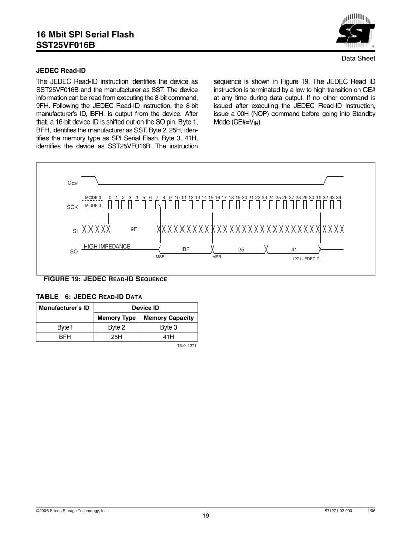
JEDEC Read-ID
The JEDEC Read-ID instruction identifies the device asSST25VF016B and the manufacturer as SST. The deviceinformation can be read from executing the 8-bit command,9FH. Following the JEDEC Read-ID instruction, the 8-bitmanufacturer’s ID, BFH, is output from the device. Afterthat, a 16-bit device ID is shifted out on the SO pin. Byte 1,BFH, identifies the manufacturer as SST. Byte 2, 25H, iden-tifies the memory type as SPI Serial Flash. Byte 3, 41H,identifies the device as SST25VF016B. The instruction
sequence is shown in Figure 19. The JEDEC Read IDinstruction is terminated by a low to high transition on CE#at any time during data output. If no other command isissued after executing the JEDEC Read-ID instruction,issue a 00H (NOP) command before going into StandbyMode (CE#=VIH).
FIGURE 19: JEDEC READ-ID SEQUENCE
25 41
1271 JEDECID.1
CE#
SO
SI
SCK
0 1 2 3 4 5 6 7 8
HIGH IMPEDANCE
15 1614 28 29 30 31
BF
MODE 3
MODE 0
MSBMSB
9 10 11 12 13 17 18 32 34
9F
19 20 21 22 23 3324 25 26 27
TABLE 6: JEDEC READ-ID DATA
Manufacturer’s ID Device ID
Memory Type Memory Capacity
Byte1 Byte 2 Byte 3
BFH 25H 41HT6.0 1271

20
Data Sheet
16 Mbit SPI Serial FlashSST25VF016B
©2006 Silicon Storage Technology, Inc. S71271-02-000 1/06
Read-ID (RDID)
The Read-ID instruction (RDID) identifies the devices asSST25VF016B and manufacturer as SST. This commandis backward compatible to all SST25xFxxxA devices andshould be used as default device identification when multi-ple versions of SPI Serial Flash devices are used in adesign. The device information can be read from executingan 8-bit command, 90H or ABH, followed by address bits[A23-A0]. Following the Read-ID instruction, the manufac-
turer’s ID is located in address 00000H and the device ID islocated in address 00001H. Once the device is in Read-IDmode, the manufacturer’s and device ID output data tog-gles between address 00000H and 00001H until termi-nated by a low to high transition on CE#.
Refer to Tables 6 and 7 for device identification data.
FIGURE 20: READ-ID SEQUENCE
1271 RdID.0
CE#
SO
SI
SCK
00
0 1 2 3 4 5 6 7 8
00 ADD190 or AB
HIGH IMPEDANCE
15 16 23 24 31 32 39 40 47 48 55 56 63
BF Device ID BF Device ID
Note: The manufacturer's and device ID output stream is continuous until terminated by a low to high transition on CE#. Device ID = 41H for SST25VF016B 1. 00H will output the manfacturer's ID first and 01H will output device ID first before toggling between the two.
HIGH IMPEDANCE
MODE 3
MODE 0
MSB MSB
MSB
TABLE 7: PRODUCT IDENTIFICATION
Address Data
Manufacturer’s ID 00000H BFH
Device ID
SST25VF016B 00001H 41HT7.0 1271
Data Sheet
16 Mbit SPI Serial FlashSST25VF016B
21©2006 Silicon Storage Technology, Inc. S71271-02-000 1/06
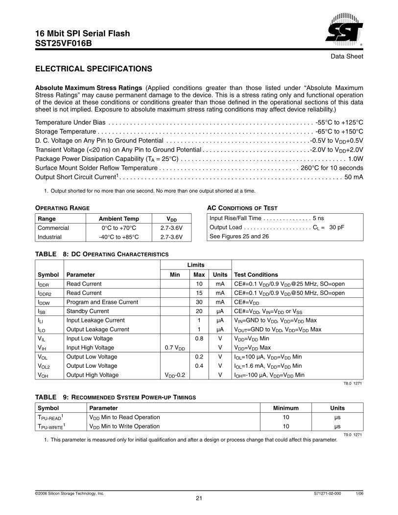
ELECTRICAL SPECIFICATIONS
Absolute Maximum Stress Ratings (Applied conditions greater than those listed under “Absolute MaximumStress Ratings” may cause permanent damage to the device. This is a stress rating only and functional operationof the device at these conditions or conditions greater than those defined in the operational sections of this datasheet is not implied. Exposure to absolute maximum stress rating conditions may affect device reliability.)
Temperature Under Bias . . . . . . . . . . . . . . . . . . . . . . . . . . . . . . . . . . . . . . . . . . . . . . . . . . . . . . . . . -55°C to +125°CStorage Temperature . . . . . . . . . . . . . . . . . . . . . . . . . . . . . . . . . . . . . . . . . . . . . . . . . . . . . . . . . . . . -65°C to +150°CD. C. Voltage on Any Pin to Ground Potential . . . . . . . . . . . . . . . . . . . . . . . . . . . . . . . . . . . . . . . . -0.5V to VDD+0.5VTransient Voltage (<20 ns) on Any Pin to Ground Potential . . . . . . . . . . . . . . . . . . . . . . . . . . . . . . -2.0V to VDD+2.0VPackage Power Dissipation Capability (TA = 25°C) . . . . . . . . . . . . . . . . . . . . . . . . . . . . . . . . . . . . . . . . . . . . . . 1.0WSurface Mount Solder Reflow Temperature . . . . . . . . . . . . . . . . . . . . . . . . . . . . . . . . . . . . . . . 260°C for 10 secondsOutput Short Circuit Current1. . . . . . . . . . . . . . . . . . . . . . . . . . . . . . . . . . . . . . . . . . . . . . . . . . . . . . . . . . . . . . 50 mA
1. Output shorted for no more than one second. No more than one output shorted at a time.
OPERATING RANGE
Range Ambient Temp VDD
Commercial 0°C to +70°C 2.7-3.6V
Industrial -40°C to +85°C 2.7-3.6V
AC CONDITIONS OF TEST
Input Rise/Fall Time . . . . . . . . . . . . . . . 5 ns
Output Load . . . . . . . . . . . . . . . . . . . . . CL = 30 pF
See Figures 25 and 26
TABLE 8: DC OPERATING CHARACTERISTICS
Symbol Parameter
Limits
Test ConditionsMin Max Units
IDDR Read Current 10 mA CE#=0.1 VDD/0.9 VDD@25 MHz, SO=open
IDDR2 Read Current 15 mA CE#=0.1 VDD/0.9 VDD@50 MHz, SO=open
IDDW Program and Erase Current 30 mA CE#=VDD
ISB Standby Current 20 µA CE#=VDD, VIN=VDD or VSS
ILI Input Leakage Current 1 µA VIN=GND to VDD, VDD=VDD Max
ILO Output Leakage Current 1 µA VOUT=GND to VDD, VDD=VDD Max
VIL Input Low Voltage 0.8 V VDD=VDD Min
VIH Input High Voltage 0.7 VDD V VDD=VDD Max
VOL Output Low Voltage 0.2 V IOL=100 µA, VDD=VDD Min
VOL2 Output Low Voltage 0.4 V IOL=1.6 mA, VDD=VDD Min
VOH Output High Voltage VDD-0.2 V IOH=-100 µA, VDD=VDD MinT8.0 1271
TABLE 9: RECOMMENDED SYSTEM POWER-UP TIMINGS
Symbol Parameter Minimum Units
TPU-READ1
1. This parameter is measured only for initial qualification and after a design or process change that could affect this parameter.
VDD Min to Read Operation 10 µs
TPU-WRITE1 VDD Min to Write Operation 10 µs
T9.0 1271

22
Data Sheet
16 Mbit SPI Serial FlashSST25VF016B
©2006 Silicon Storage Technology, Inc. S71271-02-000 1/06
TABLE 10: CAPACITANCE (TA = 25°C, f=1 Mhz, other pins open)
Parameter Description Test Condition Maximum
COUT1 Output Pin Capacitance VOUT = 0V 12 pF
CIN1 Input Capacitance VIN = 0V 6 pF
T10.0 12711. This parameter is measured only for initial qualification and after a design or process change that could affect this parameter.
TABLE 11: RELIABILITY CHARACTERISTICS
Symbol Parameter Minimum Specification Units Test Method
NEND1
1. This parameter is measured only for initial qualification and after a design or process change that could affect this parameter.
Endurance 10,000 Cycles JEDEC Standard A117
TDR1 Data Retention 100 Years JEDEC Standard A103
ILTH1 Latch Up 100 + IDD mA JEDEC Standard 78
T11.0 1271
TABLE 12: AC OPERATING CHARACTERISTICS
25 MHz 50 MHz
Symbol Parameter Min Max Min Max Units
FCLK1
1. Maximum clock frequency for Read Instruction, 03H, is 25 MHz
Serial Clock Frequency 25 50 MHz
TSCKH Serial Clock High Time 18 9 ns
TSCKL Serial Clock Low Time 18 9 ns
TSCKR2
2. Maximum Rise and Fall time may be limited by TSCKH and TSCKL requirements
Serial Clock Rise Time (Slew Rate) 0.1 0.1 V/ns
TSCKF Serial Clock Fall Time (Slew Rate) 0.1 0.1 V/ns
TCES3
3. Relative to SCK.
CE# Active Setup Time 10 5 ns
TCEH3 CE# Active Hold Time 10 5 ns
TCHS3 CE# Not Active Setup Time 10 5 ns
TCHH3 CE# Not Active Hold Time 10 5 ns
TCPH CE# High Time 100 50 ns
TCHZ CE# High to High-Z Output 15 8 ns
TCLZ SCK Low to Low-Z Output 0 0 ns
TDS Data In Setup Time 5 2 ns
TDH Data In Hold Time 5 5 ns
THLS HOLD# Low Setup Time 10 5 ns
THHS HOLD# High Setup Time 10 5 ns
THLH HOLD# Low Hold Time 10 5 ns
THHH HOLD# High Hold Time 10 5 ns
THZ HOLD# Low to High-Z Output 20 8 ns
TLZ HOLD# High to Low-Z Output 15 8 ns
TOH Output Hold from SCK Change 0 0 ns
TV Output Valid from SCK 15 8 ns
TSE Sector-Erase 25 25 ms
TBE Block-Erase 25 25 ms
TSCE Chip-Erase 50 50 ms
TBP Byte-Program 10 10 µsT12.0 1271
Data Sheet
16 Mbit SPI Serial FlashSST25VF016B
23©2006 Silicon Storage Technology, Inc. S71271-02-000 1/06
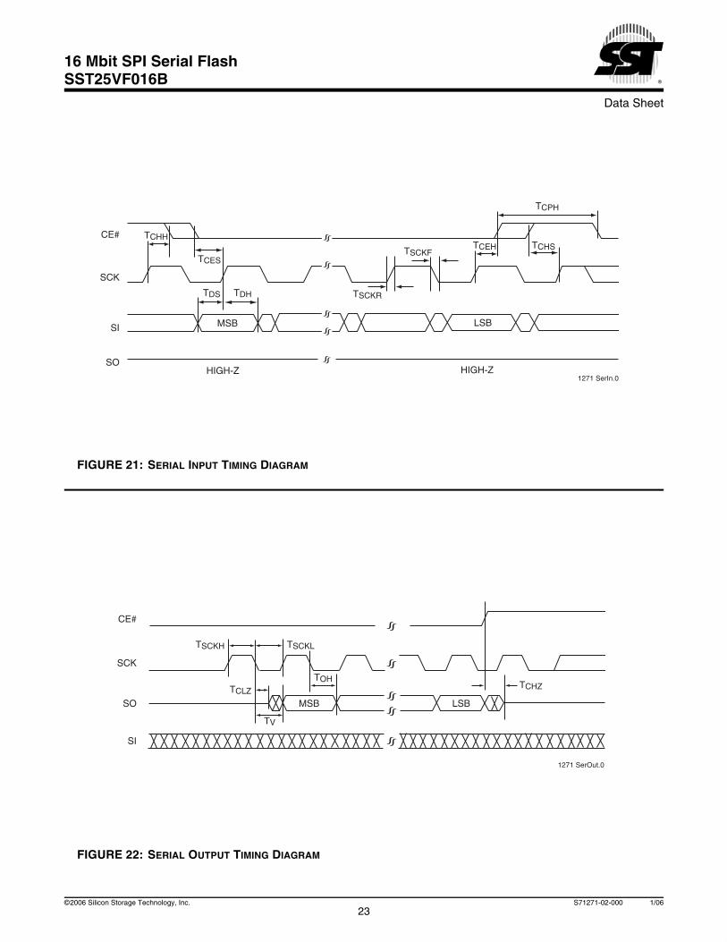
FIGURE 21: SERIAL INPUT TIMING DIAGRAM
FIGURE 22: SERIAL OUTPUT TIMING DIAGRAM
HIGH-Z HIGH-Z
CE#
SO
SI
SCK
MSB LSB
TDS TDH
TCHH
TCES
TCEH TCHS
TSCKR
TSCKF
TCPH
1271 SerIn.0
1271 SerOut.0
CE#
SI
SO
SCK
MSB
TCLZ
TV
TSCKH
TCHZTOH
TSCKL
LSB

24
Data Sheet
16 Mbit SPI Serial FlashSST25VF016B
©2006 Silicon Storage Technology, Inc. S71271-02-000 1/06
FIGURE 23: HOLD TIMING DIAGRAM
FIGURE 24: POWER-UP TIMING DIAGRAM
THZ TLZ
THHH THLS
THLH
THHS
1271 Hold.0
HOLD#
CE#
SCK
SO
SI
Time
VDD Min
VDD Max
VDD
Device fully accessibleTPU-READ
TPU-WRITE
Chip selection is not allowed.Commands may not be accepted or properly
interpreted by the device.
1271 PwrUp.0
Data Sheet
16 Mbit SPI Serial FlashSST25VF016B
25©2006 Silicon Storage Technology, Inc. S71271-02-000 1/06
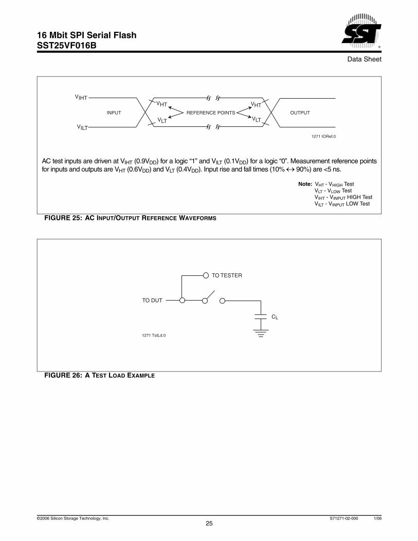
FIGURE 25: AC INPUT/OUTPUT REFERENCE WAVEFORMS
FIGURE 26: A TEST LOAD EXAMPLE
1271 IORef.0
REFERENCE POINTS OUTPUTINPUT
VHT
VLT
VHT
VLT
VIHT
VILT
AC test inputs are driven at VIHT (0.9VDD) for a logic “1” and VILT (0.1VDD) for a logic “0”. Measurement reference pointsfor inputs and outputs are VHT (0.6VDD) and VLT (0.4VDD). Input rise and fall times (10% ↔ 90%) are <5 ns.
Note: VHT - VHIGH TestVLT - VLOW TestVIHT - VINPUT HIGH TestVILT - VINPUT LOW Test
1271 TstLd.0
TO TESTER
TO DUT
CL

26
Data Sheet
16 Mbit SPI Serial FlashSST25VF016B
©2006 Silicon Storage Technology, Inc. S71271-02-000 1/06
PRODUCT ORDERING INFORMATION
Valid combinations for SST25VF016B
SST25VF016B-50-4C-S2AF SST25VF016B-50-4C-QAF
SST25VF016B-50-4I-S2AF SST25VF016B-50-4I-QAF
Note: Valid combinations are those products in mass production or will be in mass production. Consult your SST sales representative to confirm availability of valid combinations and to determine availability of new combinations.
SST 25 VF 016 B - 50 - 4C - S2A FXX XX XXX X - XX - XX - XXX X
Environmental AttributeF1 = non-Pb / non-Sn contact (lead) finish:Nickel plating with Gold top (outer) layer
Package ModifierA = 8 leads or contacts
Package TypeS2 = SOIC 200 mil body widthQ = WSON
Temperature RangeC = Commercial = 0°C to +70°CI = Industrial = -40°C to +85°C
Minimum Endurance4 = 10,000 cycles
Operating Frequency50 = 50 MHz
Device Density016 = 16 Mbit
VoltageV = 2.7-3.6V
Product Series25 = Serial Peripheral Interface flash memory
1. Environmental suffix “F” denotes non-Pb/non-SN solder. SST non-Pb/non-Sn solder devices are “RoHS Compliant”.
Data Sheet
16 Mbit SPI Serial FlashSST25VF016B
27©2006 Silicon Storage Technology, Inc. S71271-02-000 1/06
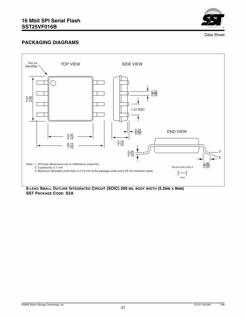
PACKAGING DIAGRAMS
8-LEAD SMALL OUTLINE INTEGRATED CIRCUIT (SOIC) 200 MIL BODY WIDTH (5.2MM X 8MM)SST PACKAGE CODE: S2A
2.161.75
08-soic-EIAJ-S2A-3Note: 1. All linear dimensions are in millimeters (max/min). 2. Coplanarity: 0.1 mm 3. Maximum allowable mold flash is 0.15 mm at the package ends and 0.25 mm between leads.
TOP VIEW SIDE VIEW
END VIEW
5.405.15
8.107.70
5.405.15
Pin #1Identifier
0.500.35
1.27 BSC
0.250.05
0.250.19
0.800.50
0˚
8˚
1mm

28
Data Sheet
16 Mbit SPI Serial FlashSST25VF016B
©2006 Silicon Storage Technology, Inc. S71271-02-000 1/06
8-CONTACT VERY-VERY-THIN SMALL OUTLINE NO-LEAD (WSON)SST PACKAGE CODE: QA
TABLE 13: REVISION HISTORY
Number Description Date
00 • Initial release of data sheet Apr 2005
01 • Corrected “JEDEC Read-ID” on page 19 including timing diagram• Corrected VHT and VLT values in Figure 25 on page 25
Sep 2005
02 • Migrated document to a Data Sheet• Updated Surface Mount Solder Reflow Temperature information
Jan 2006
Note: 1. All linear dimensions are in millimeters (max/min). 2. Untoleranced dimensions (shown with box surround) are nominal target dimensions. 3. The external paddle is electrically connected to the die back-side and possibly to certain VSS leads. This paddle can be soldered to the PC board; it is suggested to connect this paddle to the VSS of the unit. Connection of this paddle to any other voltage potential can result in shorts and/or electrical malfunction of the device.
8-wson-5x6-QA-9.0
4.0
1.27 BSC
Pin #1
0.480.35
0.076
3.4
5.00 ± 0.10
6.00 ± 0.100.05 Max
0.700.50
0.800.70
0.800.70
Pin #1Corner
TOP VIEW BOTTOM VIEW
CROSS SECTION
SIDE VIEW
1mm
0.2
Silicon Storage Technology, Inc. • 1171 Sonora Court • Sunnyvale, CA 94086 • Telephone 408-735-9110 • Fax 408-735-9036www.SuperFlash.com or www.sst.com
Related Documents