1/12 Axelite Confidential Materials, do not copy or distribute without written consent. Rev.1.5 Jun.06, 2007 AX3001 150KHz, 2A PWM Buck DC/DC Converter GENERAL DESCRIPTION The AX3001 series are monolithic IC designed for a step-down DC/DC converter, and own the ability of driving a 2A load without additional transistor. It saves board space. The external shutdown function can be controlled by logic level and then come into standby mode. The internal compensation makes feedback control having good line and load regulation without external design. Regarding protected function, thermal shutdown is to prevent over temperature operating from damage, and current limit is against over current operating of the output switch. If current limit function occurs and V FB is down below 0.5V, the switching frequency will be reduced. The AX3001 series operates at a switching frequency of 150KHz thus allow smaller sized filter components than what would be needed with lower frequency switching regulators. Other features include a guaranteed +4% tolerance on output voltage under specified input voltage and output load conditions, and +15% on the oscillator frequency. The output version included fixed 3.3V, 5V, 12V, and an adjustable type. The chips are available in a standard 8-lead SOP package. FEATURES - Output voltage: 3.3V, 5V, 12V and adjustable output version. - Adjustable version output voltage range, 1.23V to 19.5V+4%. - 150KHz +15% fixed switching frequency. - Voltage mode non-synchronous PWM control. - Thermal-shutdown and current-limit protection. - ON/OFF shutdown control input. - Short Circuit Protect (SCP). - Operating voltage can be up to 22V. - Output load current: 2A. - SOP-8L Pb-Free packages. - Low power standby mode. - Built-in switching transistor on chip. 授权代理商:深圳市四海恒通科技有限公司 电话:0755-8398 3377 135 9011 2223 http://www.gofotech.com

Welcome message from author
This document is posted to help you gain knowledge. Please leave a comment to let me know what you think about it! Share it to your friends and learn new things together.
Transcript

1/12
Axelite Confidential Materials, do not copy or distribute without written consent. Rev.1.5 Jun.06, 2007
AX3001
150KHz, 2A PWM Buck DC/DC Converter
GENERAL DESCRIPTION The AX3001 series are monolithic IC designed for a step-down DC/DC converter,
and own the ability of driving a 2A load without additional transistor. It saves board space. The external shutdown function can be controlled by logic level and then come into standby mode. The internal compensation makes feedback control having good line and load regulation without external design. Regarding protected function, thermal shutdown is to prevent over temperature operating from damage, and current limit is against over current operating of the output switch. If current limit function occurs and VFB is down below 0.5V, the switching frequency will be reduced. The AX3001 series operates at a switching frequency of 150KHz thus allow smaller sized filter components than what would be needed with lower frequency switching regulators. Other features include a guaranteed +4% tolerance on output voltage under specified input voltage and output load conditions, and +15% on the oscillator frequency. The output version included fixed 3.3V, 5V, 12V, and an adjustable type. The chips are available in a standard 8-lead SOP package.
FEATURES - Output voltage: 3.3V, 5V, 12V and adjustable output version. - Adjustable version output voltage range, 1.23V to 19.5V+4%. - 150KHz +15% fixed switching frequency. - Voltage mode non-synchronous PWM control. - Thermal-shutdown and current-limit protection. - ON/OFF shutdown control input. - Short Circuit Protect (SCP). - Operating voltage can be up to 22V. - Output load current: 2A. - SOP-8L Pb-Free packages. - Low power standby mode. - Built-in switching transistor on chip.
授权代理商:深圳市四海恒通科技有限公司 电话:0755-8398 3377 135 9011 2223 http://www.gofotech.com

2/12
Axelite Confidential Materials, do not copy or distribute without written consent. Rev.1.5 Jun.06, 2007
150KHz, 2A PWM Buck DC/DC Converter AX3001
BLOCK DIAGRAM
150kHzOSC.
START UP
+
+
_
+_
ThermalShutdown
CONTROL +
DRIVER
COMP.
COMP.
Vss
SW
EN
FB
200mV
220mV
SWITCH
_
COMP.
VCC
Current limit
+_AMP
COMP.
CURRENTSOURCE
BIAS
1.235V
REFERENCE2.5V
REGULATOR
R2
R1
ADJ : R2=0Ω, R1=OPEN
PIN ASSIGNMENT The package of AX3001 is SOP-8L; the pin assignment is given by:
Name Description
VCC Operating voltage input
SW Switching output
FB Output voltage feedback control
EN ON/OFF Shutdown
SW
EN
Vcc
FB
Vss
VssVss
Vss
1
32
4
8
67
5
SOP-8L
(Top View)
VSS GND pin
授权代理商:深圳市四海恒通科技有限公司 电话:0755-8398 3377 135 9011 2223 http://www.gofotech.com

3/12
Axelite Confidential Materials, do not copy or distribute without written consent. Rev.1.5 Jun.06, 2007
150KHz, 2A PWM Buck DC/DC Converter AX3001
ORDER INFORMATION
Order Information
AX3001- XX X X
Package Type S: SOP-8L
PackingBlank : TubeA : Taping
33:3.3V50:5.0V12: 12V
Blank:ADJ
Output Voltage
MARKING INFORMATION
Top Marking ADJ
X X X X X AX
3001Logo
ID code: internalWW: 01~52Year : 06 = 2006
Part number
FIX
X X X X X AX
3001Logo Output VoltageID code: internalWW: 01~52Year : 06 = 2006
-50Part number
授权代理商:深圳市四海恒通科技有限公司 电话:0755-8398 3377 135 9011 2223 http://www.gofotech.com

4/12
Axelite Confidential Materials, do not copy or distribute without written consent. Rev.1.5 Jun.06, 2007
150KHz, 2A PWM Buck DC/DC Converter AX3001
Absolute Maximum Ratings
Characteristics Symbol Rating Unit Maximum Supply Voltage VCC +24 V ON/OFF Pin Input Voltage VEN -0.3 to VCC V Feedback Pin Voltage VFB -0.3 to 16 V Output Voltage to Ground VOUT -0.8 V Power Dissipation Internally limited PD ( TJ-TA ) / θJA W Storage Temperature Range TST -65 to +150 ℃ Operating Temperature Range TOP -20 to +125 ℃ Operating Supply Voltage VOP +4.5 to +22 V Thermal Resistance from Junction to case θJC 20 /W℃ Thermal Resistance from Junction to ambient θJA 60 /W℃
Note : θJA is measured with the PCB copper area(need connect to VSS pins) of approximately 1.5 in2 (Multi-layer).
Electrical Characteristics (Unless otherwise specified, Ta=25°C, VCC=12V for 3.3V, 5V, adjustable version and VCC=18V for the 12V version. ILOAD = 0.2A)
Characteristics Symbol Conditions Min Typ Max Units Quiescent Current IQ VFB=12V force driver off 4 8 mA
-50 Feedback bias current IFB VFB=1.3V (Adjustable version only) -10 -100 nA
100 Shutdown supply Current ISD EN pin=5V VCC=22V 35 100 uA
127 150 173 Oscillator frequency FOSC
110 173 KHz
(Adjustable) When VFB<0.5V 50 KHz Oscillator frequency of short circuit protect FSCP (Fixed)When < VOUT*40% 50 KHz Max. Duty Cycle (ON) VFB=12V force driver on 0 Min. Duty Cycle (OFF)
DC VFB=0V force driver off 100
%
Current limit ICL Pear current, No outside circuit V FB=0V force driver on 2.4 A
1.4 Saturation voltage VSA T IOUT=2A, No outside circuit VFB=0V force driver on 1.2
1.5 V
SW pin=0V No outside circuit VFB=12V force driver off -200 uA
SW pin=-0.8V
SW pin leakage current
ISW L VCC=22V force driver off -5 mA
VIL Low (regulator ON) - 0.6 EN pin logic input threshold voltage VIH High (regulator OFF) 2.0
1.3 -
V
EN pin logic input current IH VEN=2.5V (OFF) -0.1 -0.5 EN pin input current IL VEN=0.5V (ON) -0.01
uA
Thermal shutdown Temp TSD 135 ℃
授权代理商:深圳市四海恒通科技有限公司 电话:0755-8398 3377 135 9011 2223 http://www.gofotech.com

5/12
Axelite Confidential Materials, do not copy or distribute without written consent. Rev.1.5 Jun.06, 2007
150KHz, 2A PWM Buck DC/DC Converter AX3001
Electrical Characteristics (Continued)
Specifications with boldface type are for full operating temperature range, the other type are for TJ=25ºC.
version Characteristics Symbol Conditions Min Typ Max Units
Output Feedback
voltage V FB
4.5V < VCC < 22V
0. 2A < ILOAD < 2A
VOUT programmed
for 3.3V
1.193
/1.180 1.23
1.267
/1.280 V
AX3001-ADJ
Efficiency η VCC = 12V, ILOAD=2A 80 %
Output voltage V OUT 4.75V < VCC < 22V
0.2A < ILOAD < 2A 3.168
/3.135 3.3
3.432
/3.465 V
AX3001-3.3V
Efficiency η VCC = 12V, ILOAD=2A 81 %
Output voltage V OUT 7V < VCC < 22V
0.2A < ILOAD < 2A 4.80
/4.75 5.0
5.20
/5.25 V
AX3001-5.0V
Efficiency η VCC = 12V, ILOAD=2A 85 %
Output voltage V OUT 15V < VCC < 22V
0.2A < ILOAD < 2A 11.52
/11.40 12
12.48
/12.60 V
AX3001-12V
Efficiency η VCC = 15V, ILOAD = 2A 91 %
授权代理商:深圳市四海恒通科技有限公司 电话:0755-8398 3377 135 9011 2223 http://www.gofotech.com

6/12
Axelite Confidential Materials, do not copy or distribute without written consent. Rev.1.5 Jun.06, 2007
150KHz, 2A PWM Buck DC/DC Converter AX3001
Application Circuit
(1) Adjustable Output Voltage Version
C20.1uF
D1B340A
L1
33uH1 2
C3470uF
C1470uF
U1
AX3001
1
2
3
4 5
6
7
8Vcc
SW
FB
EN Vss
Vss
Vss
VssC510nF
VIN=12V
ON/OFF
C60.1uF R2
1.5K
R14.7K
Vout=5.0V/2A
Vout = VFB × (1 +R2R1 )
VFB = 1.23V R2 = 0.47K ~ 2.6K
Table 1 Resistor select for output voltage setting VOUT R2 R1
1.5K 4.7K 5V
1.8K 5.6K 1.5K 2.5K
3.3V 1.8K 3.0K
2.5V 1.8K 1.8K 1.8V 1.8K 0.82K
(2) Fixed Output Voltage Version
C1470uF
Vout=3.3V/2AVIN=12V
C20.1uF
D1B240A
L1
33uH1 2
C3470uF
U1
AX3001-33
1
2
3
4 5
6
7
8Vcc
SW
FB
EN Vss
Vss
Vss
Vss
C60.1uF
授权代理商:深圳市四海恒通科技有限公司 电话:0755-8398 3377 135 9011 2223 http://www.gofotech.com
7/12
Axelite Confidential Materials, do not copy or distribute without written consent. Rev.1.5 Jun.06, 2007
150KHz, 2A PWM Buck DC/DC Converter AX3001
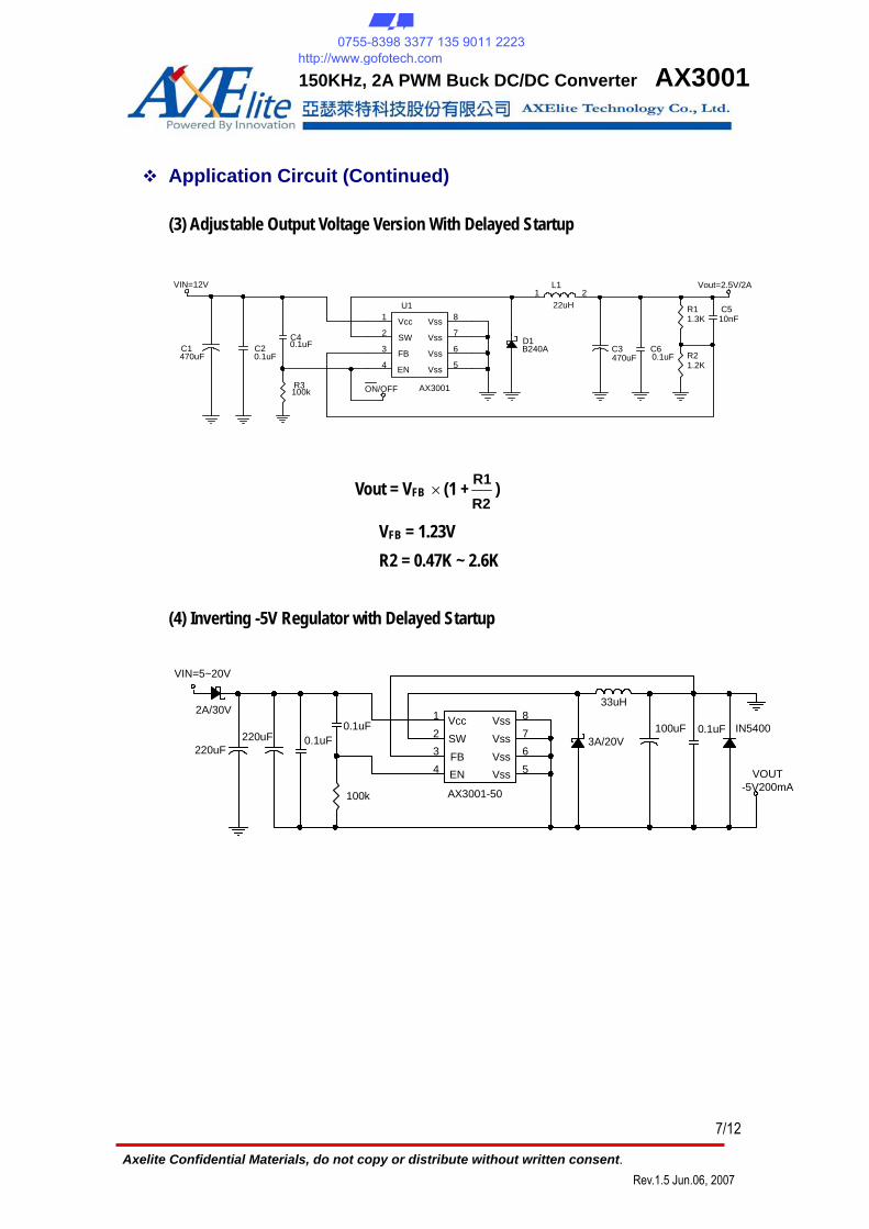
Application Circuit (Continued)
(3) Adjustable Output Voltage Version With Delayed Startup
C20.1uF
D1B240A
L1
22uH1 2
C3470uF
C1470uF
U1
AX3001
1
2
3
4 5
6
7
8Vcc
SW
FB
EN Vss
Vss
Vss
Vss
Vout=2.5V/2A
C510nF
VIN=12V
ON/OFF
C60.1uF R2
1.2K
R11.3K
C40.1uF
R3100k
Vout = VFB × (1 +R2R1 )
VFB = 1.23V R2 = 0.47K ~ 2.6K
(4) Inverting -5V Regulator with Delayed Startup
IN5400220uF 0.1uF 3A/20V
VIN=5~20V
AX3001-50
1234 5
678Vcc
SWFBEN Vss
VssVssVss
100uF0.1uF
100k
2A/30V
220uF
33uH
0.1uF
VOUT -5V200mA
授权代理商:深圳市四海恒通科技有限公司 电话:0755-8398 3377 135 9011 2223 http://www.gofotech.com

8/12
Axelite Confidential Materials, do not copy or distribute without written consent. Rev.1.5 Jun.06, 2007
150KHz, 2A PWM Buck DC/DC Converter AX3001
Function Descriptions
Pin Functions Vcc
This is the positive input supply for the IC switching regulator. A suitable input bypass capacitor must be presented at this pin to minimize voltage transients and to supply the switching currents needed by the regulator.
Vss
Circuit ground.
SW Internal switch. The voltage at this pin switches between (+VCC – VSAT) and
approximately – 0.5V, with a duty cycle of approximately VOUT / VCC. To minimize coupling to sensitive circuitry, the PC board copper area connected to this pin should be minimized.
Feedback
Senses the regulated output voltage to complete the feedback loop.
EN Allows the switching regulator circuit to be shutdown using logic level signals thus
dropping the total input supply current to approximately 100uA. Pulling this pin below a threshold voltage of approximately 1.3V turns the regulator on, and pulling this pin above 1.3V (up to a maximum of Vcc) shuts the regulator down. If this shutdown feature is not needed, the EN pin can be wired to the ground pin.
Thermal Considerations The SOP-8 package needs a heat sink under most conditions. The size of the
heat sink depends on the input voltage, the output voltage, the load current and the ambient temperature. The AX3001 junction temperature rises above ambient temperature for a 2A load and different input and output voltages.
The data for these curves was taken with the AX3001 (SOP-8 package) operating as a buck-switching regulator in an ambient temperature of 25℃ (still air). These temperature increments are all approximate and are affected by many factors. Higher ambient temperatures requires more heat sinker.
授权代理商:深圳市四海恒通科技有限公司 电话:0755-8398 3377 135 9011 2223 http://www.gofotech.com

9/12
Axelite Confidential Materials, do not copy or distribute without written consent. Rev.1.5 Jun.06, 2007
150KHz, 2A PWM Buck DC/DC Converter AX3001
Function Descriptions (Continued) For the best thermal performance, wide copper traces and generous amounts of
printed circuit board copper (need connect to the VSS pins) should be used in the board layout, (One exception is the SW(switch) pin, which should not have large areas of copper.) Large areas of copper provide the best transfer of heat (lower thermal resistance) to the surrounding air, and moving air lowers the thermal resistance even further.
Package thermal resistance and junction temperature increments are all approximate. The increments are affected by a lot of factors. Some of these factors include board size, shape, thickness, position, location, and even board temperature. Other factors are, trace width, total printed circuit copper area, copper thickness, single or double-sided, multi-layer board and the amount of solder on the board.
The effectiveness of the PC board to dissipate heat also depends on the size, quantity and spacing of other components on the board, as well as whether the surrounding air is still or moving. Furthermore, some of these components such as the
catch diode will add heat to the PC board and the heat can vary as the input voltage
changes. For the inductor, depending on the physical size, type of core material and the
DC resistance, it could either act as a heat sink taking heat away from the board, or it
could add heat to the board.
授权代理商:深圳市四海恒通科技有限公司 电话:0755-8398 3377 135 9011 2223 http://www.gofotech.com

10/12
Axelite Confidential Materials, do not copy or distribute without written consent. Rev.1.5 Jun.06, 2007
150KHz, 2A PWM Buck DC/DC Converter AX3001
Typical Characteristics
VOUT VS VIN ICCQ VS VIN
VOUT VS VIN
3.15
3.20
3.25
3.30
3.35
3.40
3.45
4 6 8 10 12 14 16 18 20 22 24Vin(V)
Vou
t(V)
Iccq VS VIN
0.00
1.00
2.00
3.00
4.00
5.00
6.00
4 6 8 10 12 14 16 18 20 22 24Vin(V)
Iccq
(mA
)
FOSC VS VIN
FOSC VS TEMPERATURE
Fosc VS VIN
140
145
150
155
160
165
170
4 6 8 10 12 14 16 18 20 22 24Vin(V)
Fosc
(KH
z)
FOSC VS TEMP
120
130
140
150
160
170
180
-20 0 20 40 60 80 100 120temp (℃)
Vou
t(V)
VFB VS TEMPERATURE
ICCQ VS TEMPERATURE
VFB VS TEMP
1.18
1.20
1.22
1.24
1.26
1.28
-20 0 20 40 60 80 100 120temp (℃)
Vou
t(V)
ICCQ VS TEMP
0.00
1.00
2.00
3.00
4.00
5.00
6.00
-20 0 20 40 60 80 100 120temp (℃)
Vou
t(V)
授权代理商:深圳市四海恒通科技有限公司 电话:0755-8398 3377 135 9011 2223 http://www.gofotech.com

11/12
Axelite Confidential Materials, do not copy or distribute without written consent. Rev.1.5 Jun.06, 2007
150KHz, 2A PWM Buck DC/DC Converter AX3001
Typical Characteristics
Output Ripple
(VIN=12V, VOUT=3.3V, IOUT=2A)
Power on test wave
(VIN=12V, VOUT=5V, IOUT=2A )
Load Transient Response
(VIN=12V, VOUT=5V, IOUT=0.1~2A)
EN on test wave
(VIN=12V, VOUT=5V, IOUT=2A )
Efficiency
(VIN=12V, VOUT=3.3V)
Efficiency
(VIN=12V, VOUT=5.0V)
Vin=12V
0%
10%
20%
30%
40%
50%
60%
70%
80%
90%
0.0 0.5 1.0 1.5 2.0Iout(A)
Effi
cien
cy(%
)
Vin=12V
0%
10%
20%
30%
40%
50%
60%
70%
80%
90%
0.0 0.5 1.0 1.5 2.0Iout(A)
Effic
ienc
y(%
)
SW
ISW
SW
ISW
VOUT
VIN
VOUT (AC)
SW
ISW
VOUT (AC)
SW
ISW
VOUT VIN
授权代理商:深圳市四海恒通科技有限公司 电话:0755-8398 3377 135 9011 2223 http://www.gofotech.com

12/12
Axelite Confidential Materials, do not copy or distribute without written consent. Rev.1.5 Jun.06, 2007
150KHz, 2A PWM Buck DC/DC Converter AX3001
Package Outlines
DETAIL A
LHE
AA2
A1e
D
7 (4X)
b
y
C
DETAIL A
Dimensions In Millimeters Dimensions In Inches Symbol Min. Nom. Max. Min. Nom. Max. A 1.40 1.60 1.75 0.055 0.063 0.069
A1 0.10 - 0.25 0.040 - 0.100 A2 1.30 1.45 1.50 0.051 0.057 0.059 C 0.19 0.20 0.25 0.0075 0.008 0.010 D 4.80 4.90 5.00 0.189 0.193 0.197 E 3.80 3.90 4.00 0.150 0.154 0.157 H 5.79 5.99 6.20 0.228 0.236 0.244 L 0.38 0.71 1.27 0.015 0.028 0.050 b 0.33 0.41 0.51 0.013 0.016 0.020 e 1.27 TYP 0.050 TYP y - - 0.10 - - 0.004 θ 0O - 8O 0O - 8O
授权代理商:深圳市四海恒通科技有限公司 电话:0755-8398 3377 135 9011 2223 http://www.gofotech.com
Related Documents