1.5 Gbit/s Multi-Channel Visible Light Communications Using CMOS-Controlled GaN-Based LEDs Author Zhang, Shuailong, Watson, Scott, J. D. McKendry, Jonathan, Massoubre, David, Cogman, Andrew, Gu, Erdan, K. Henderson, Robert, E. Kelly, Anthony, D. Dawson, Martin Published 2013 Journal Title Journal of Lightwave Technology DOI https://doi.org/10.1109/JLT.2013.2246138 Copyright Statement © 2012 IEEE. Personal use of this material is permitted. Permission from IEEE must be obtained for all other uses, in any current or future media, including reprinting/republishing this material for advertising or promotional purposes, creating new collective works, for resale or redistribution to servers or lists, or reuse of any copyrighted component of this work in other works. Downloaded from http://hdl.handle.net/10072/51690 Griffith Research Online https://research-repository.griffith.edu.au

Welcome message from author
This document is posted to help you gain knowledge. Please leave a comment to let me know what you think about it! Share it to your friends and learn new things together.
Transcript

1.5 Gbit/s Multi-Channel Visible Light CommunicationsUsing CMOS-Controlled GaN-Based LEDs
Author
Zhang, Shuailong, Watson, Scott, J. D. McKendry, Jonathan, Massoubre, David, Cogman,Andrew, Gu, Erdan, K. Henderson, Robert, E. Kelly, Anthony, D. Dawson, Martin
Published
2013
Journal Title
Journal of Lightwave Technology
DOI
https://doi.org/10.1109/JLT.2013.2246138
Copyright Statement
© 2012 IEEE. Personal use of this material is permitted. Permission from IEEE must beobtained for all other uses, in any current or future media, including reprinting/republishing thismaterial for advertising or promotional purposes, creating new collective works, for resale orredistribution to servers or lists, or reuse of any copyrighted component of this work in otherworks.
Downloaded from
http://hdl.handle.net/10072/51690
Griffith Research Online
https://research-repository.griffith.edu.au

Abstract—An on-chip multi-channel visible light
communication (VLC) system is realized through a blue
(450 nm) GaN-based micron-size light-emitting diode
(µLED) array integrated with complementary
metal-oxide-semiconductor (CMOS) electronics. When
driven by a custom-made CMOS driving board with 16
independent parallel data input ports, this µLED array
device is computer controllable via a standard USB
interface and is capable of delivering high speed parallel
data streams for VLC. A total maximum error-free data
transmission rate of 1.5 Gbit/s is achieved in free space by
modulating four µLED pixels simultaneously using an
on-off key non-return to zero modulation scheme. Electrical
and optical crosstalk of the system has also been
investigated in detail and the further optimization of CMOS
design to minimize the crosstalk is proposed.
Index Terms—Multi-channel, parallel data transmission,
spatial-multiplexing, visible light communication (VLC), micro
light-emitting diodes (µLEDs), complementary
metal-oxide-semiconductor (CMOS).
I. INTRODUCTION
igh-performance III-Nitride light-emitting diodes (LEDs)
have the capability of efficiently generating light across the
visible spectrum, which enables a variety of applications such as
signaling, displays and solid-state lighting [1] [2]. For general
illumination, high power III-N-based white LEDs have shown
superior capabilities over incandescent and fluorescent lamps in
terms of efficiency and other attributes [1]. In addition to their
appealing lighting properties, another promising application of
LEDs is for visible light communication (VLC) [3] [4]. It is
possible to achieve LED illumination and optical data
transmission simultaneously, providing energy-efficient light
sources with data encoded in them for dual applications. LED
VLC has attracted much interest recently, as it is believed that
this technology could provide new data transmission capacity
and be widely used in future wireless systems [5]. Furthermore,
S. Zhang, J. J. D. McKendry, D. Massoubre, E. Gu, and M. D. Dawson are
with the Institute of Photonics, University of Strathclyde, SUPA, Glasgow, G4
0NW, U.K. S. Zhang and E. Gu are also with the Joint Laboratory of Advanced
Optoelectronic Materials and Devices, State Key Laboratory, Wuhan University
of Technology, China. (e-mail: [email protected]).
S. Watson and A. E. Kelly are with the School of Engineering, University of
Glasgow, Glasgow, G12 8QQ, U.K.
A. Cogman and R. K. Henderson are with the Joint Research Institute for
Integrated Systems, Institute for Micro and Nano Systems, School of
Engineering, University of Edinburgh, Edinburgh, EH9 3JL, U.K.
by exploiting the low-loss transmission window in polymer
optical fiber (POF), LEDs emitting at blue and green regime
could be used for POF-based optical communication as well.
Recently, 1.07-Gb/s data transmissions over a 50-m SI-POF
fiber has been successfully demonstrated using a specifically
designed cyan LED device [6].
However, the modulation bandwidth of conventional
commercial LEDs for lighting is generally low [7] [8] and to
improve the performance of these low-bandwidth transmitters
for VLC, various advanced modulation and demodulation
schemes, such as the orthogonal frequency division
multiplexing (OFDM) modulation technique, have been
proposed and developed [9] [10]. Recently, we have
demonstrated that GaN-based micron-size LEDs (µLEDs) have
very wide modulation bandwidths [11], which makes them ideal
high-speed data sources for optical data transmission [12].
To significantly increase VLC data transmission capacity,
optical wireless multiple-input multiple-output (MIMO)
systems have been developed [13]-[15]. The idea of optical
wireless MIMO is to modulate a number of individual light
sources simultaneously for data transmission, thus realizing
high-speed parallel data streams for communication. An optical
MIMO system could greatly enhance the system data
transmission capacity compared with a
single-input/single-output system, and thus has drawn much
attention recently [16]. Most of the current optical MIMO
systems are based on separate LED devices.
In an earlier paper, we have reported a complementary
metal-oxide-semiconductor (CMOS)-controlled µLED array,
allowing individual µLED pixels from the array to be readily
controlled via a simple computer interface while retaining high
modulation bandwidth (up to 185 MHz) [11]. Although the
CMOS chip was not designed for the purpose VLC, 512 Mbit/s
data transmission based on a single pixel from such a
CMOS-controlled µLED array was demonstrated. In this work,
we further investigate the modulation capability of
CMOS-controlled multiple µLED pixels in parallel with
independent data input per pixel and demonstrate, for the first
time, an easily-controlled on-chip optical multi-transmitter
VLC system based on a single µLED array device. By
simultaneously modulating four 450 nm-emitting 99×99 µm2
CMOS-controlled µLED pixels using on-off key (OOK)
modulation scheme, non-return-to zero (NRZ) data streams at a
bit rate of up to 375 Mbit/s per pixel has been achieved. Error
free operation, defined as a Bit Error Ratio (BER) of less than
1×10⁻¹⁰, is confirmed for all of the data channels, giving a total
bit rate of 1.5 Gbit/s. This establishes a baseline demonstration
of the interest parallelism of these µLED arrays and opens the
way to further multi-channel scaling.
1.5 Gbit/s multi-channel visible light communications using
CMOS-controlled GaN-based LEDs
Shuailong Zhang, Scott Watson, Jonathan J. D. McKendry, David Massoubre, Andrew Cogman, Erdan
Gu, Robert K. Henderson, Anthony E. Kelly and Martin D. Dawson, Fellow, IEEE
H
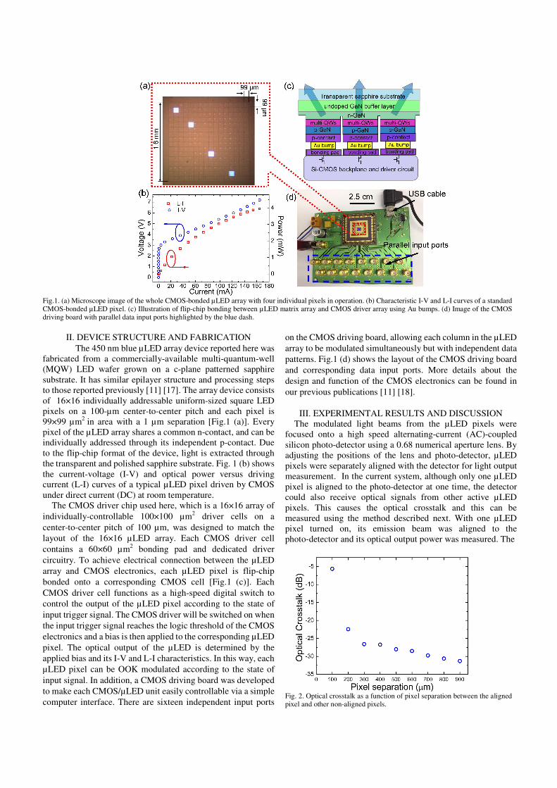
Fig.1. (a) Microscope image of the whole CMOS-bonded µLED array with four individual pixels in operation. (b) Characteristic I-V and L-I curves of a standard CMOS-bonded µLED pixel. (c) Illustration of flip-chip bonding between µLED matrix array and CMOS driver array using Au bumps. (d) Image of the CMOS driving board with parallel data input ports highlighted by the blue dash.
II. DEVICE STRUCTURE AND FABRICATION
The 450 nm blue µLED array device reported here was
fabricated from a commercially-available multi-quantum-well
(MQW) LED wafer grown on a c-plane patterned sapphire
substrate. It has similar epilayer structure and processing steps
to those reported previously [11] [17]. The array device consists
of 16×16 individually addressable uniform-sized square LED
pixels on a 100-µm center-to-center pitch and each pixel is
99×99 µm2
in area with a 1 µm separation [Fig.1 (a)]. Every
pixel of the µLED array shares a common n-contact, and can be
individually addressed through its independent p-contact. Due
to the flip-chip format of the device, light is extracted through
the transparent and polished sapphire substrate. Fig. 1 (b) shows
the current-voltage (I-V) and optical power versus driving
current (L-I) curves of a typical µLED pixel driven by CMOS
under direct current (DC) at room temperature.
The CMOS driver chip used here, which is a 16×16 array of
individually-controllable 100×100 µm2 driver cells on a
center-to-center pitch of 100 µm, was designed to match the
layout of the 16×16 µLED array. Each CMOS driver cell
contains a 60×60 µm2 bonding pad and dedicated driver
circuitry. To achieve electrical connection between the µLED
array and CMOS electronics, each µLED pixel is flip-chip
bonded onto a corresponding CMOS cell [Fig.1 (c)]. Each
CMOS driver cell functions as a high-speed digital switch to
control the output of the µLED pixel according to the state of
input trigger signal. The CMOS driver will be switched on when
the input trigger signal reaches the logic threshold of the CMOS
electronics and a bias is then applied to the corresponding µLED
pixel. The optical output of the µLED is determined by the
applied bias and its I-V and L-I characteristics. In this way, each
µLED pixel can be OOK modulated according to the state of
input signal. In addition, a CMOS driving board was developed
to make each CMOS/µLED unit easily controllable via a simple
computer interface. There are sixteen independent input ports
on the CMOS driving board, allowing each column in the µLED
array to be modulated simultaneously but with independent data
patterns. Fig.1 (d) shows the layout of the CMOS driving board
and corresponding data input ports. More details about the
design and function of the CMOS electronics can be found in
our previous publications [11] [18].
III. EXPERIMENTAL RESULTS AND DISCUSSION
The modulated light beams from the µLED pixels were
focused onto a high speed alternating-current (AC)-coupled
silicon photo-detector using a 0.68 numerical aperture lens. By
adjusting the positions of the lens and photo-detector, µLED
pixels were separately aligned with the detector for light output
measurement. In the current system, although only one µLED
pixel is aligned to the photo-detector at one time, the detector
could also receive optical signals from other active µLED
pixels. This causes the optical crosstalk and this can be
measured using the method described next. With one µLED
pixel turned on, its emission beam was aligned to the
photo-detector and its optical output power was measured. The
Fig. 2. Optical crosstalk as a function of pixel separation between the aligned pixel and other non-aligned pixels.

Fig. 3. Frequency response curve of a typical CMOS/µLED pixel, with a forward bias of 6.5 V. The optical -3 dB bandwidth is 147.9 MHz.
pixel was then turned off and without changing the alignment of
the photo-detector, adjacent non-aligned pixels were switched
on individually and the optical power coupled to the
photo-detector was recorded. The optical power from the
aligned µLED pixel was then compared with the optical power
received from the other non-aligned µLED pixels, and thus, the
optical crosstalk could be quantified. Fig.2. shows the optical
crosstalk (in dB) as a function of the center-to-center pixel
separation between aligned µLED pixel and other non-aligned
µLED pixels. As shown in Fig.2, when using the µLED pixels
next to each other (pixel separation 100 µm) for parallel data
transmission, the optical crosstalk is approximately -6 dB,
which could influence the system performance. However, when
the pixel separation reaches 200 µm and above, the optical
crosstalk is less than -25 dB. Therefore, in our present system
we can effectively neglect optical crosstalk by selecting the
active µLED pixels with a minimum spatial distance of 200µm.
The optics used in the current system was chosen for
characterizing the performance of the CMOS/µLED pixels, and
it is noted that the optical crosstalk will vary depending on how
the light is collected at the detector. By using specifically
designed optics, such as integrated micro-lenses [19], it should
be possible to modify the beam profile from the µLEDs and thus
reduce the optical crosstalk between two adjacent pixels in due
course.
The frequency response of a single CMOS/µLED pixel was
measured by the silicon photo-detector and a network analyzer.
The output from the network analyzer was combined with a DC
offset to reach the logic threshold of the CMOS electronics and
then sent to the CMOS driving board through the parallel data
input to modulate the corresponding µLED pixel. The optical
response of the µLED pixel was then detected by the fast
photo-detector and the electrical output of the detector was fed
back to the network analyzer. Fig.3 shows the frequency
response of a representative µLED pixel at an applied bias of 6.5
V. From this measurement, the optical -3 dB bandwidth of the
µLED pixel CMOS combination was found to be approximately
150 MHz. As shown in Fig.3, there is a sudden drop in the
frequency response at around 500 MHz, which is due to the
digital characteristic of the CMOS circuit. The present CMOS
drivers are not able to be switched on and off in response to very
high-frequency signals, therefore, they are effectively in the off
Fig. 4. Eye diagrams of a typical CMOS/µLED pixel when it is modulated at
375 Mbit/s in (a) one channel, (b) two channels, (c) three channels and (d) four
channels. The applied bias is 6.5 V.
state above 550 MHz. To test the bandwidth uniformity of the
µLED array, fourteen pixels along the diagonal of the array
were sampled and the optical -3 dB modulation bandwidth was
measured to be 145 MHz ±10 MHz for all of the pixels. A
detailed investigation of the frequency response of other
CMOS-bonded µLED devices and the corresponding method to
fit the frequency response curve has been reported earlier [11].
The bandwidth of CMOS-controlled µLED is lower than the
‘bare’ µLED (unbonded device) driven directly with a
high-speed probe [12], which is largely due to the frequency
response of the CMOS driver itself and the high modulation
depth of the CMOS driver output. However, it is expected that
an optimized design of the CMOS driver would enable much
higher bandwidth.
Data transmission was carried out using four individual
µLED pixels. The reason that four µLED pixels was chosen to
carry out the data transmission measurement is that we believe
using four µLED pixels is enough to prove the concept of
parallel data transmission using this CMOS/µLED device and
allow issues such as crosstalk to be examined. In this data
transmission measurement, four separate data sources with a
common clock frequency were used. The four data signals were
all OOK-NRZ pseudo-random binary sequence with a standard
pattern length of 27-1 bits and a peak-to-peak voltage swing of 0
to 2V. The data signals reaching the logic threshold of the
CMOS electronics were sent to the CMOS chip through four
parallel inputs to trigger four independently-addressable CMOS
drivers directly, and in this way, the four corresponding µLED
pixels could be modulated simultaneously with different data
patterns. The spatial separation between the modulated µLED
pixels was kept above 600 µm and in this case, the optical
crosstalk in this multi-channel system is less than -25dB (Fig.2),
thus negligible.
A typical eye diagram from an individual pixel (aligned to the
detector) modulated at 375 Mbit/s and with a 6.5 V applied bias
is shown in Fig. 4 (a). The eye diagrams of this aligned pixel
when two, three and four µLED pixels are modulated
simultaneously at 375 Mbit/s with a 6.5 V applied bias are
shown in Fig. 4 (b), (c) and (d), respectively. It can be noted that
the eye quality degrades with increasing number of modulated
pixels (channels), indicating the presence of electrical crosstalk,
as the optical crosstalk is negligible in this configuration.

Fig. 5. Bit-error ratios measured from the CMOS/µLED pixel at 375 Mbit/s,
with one channel, two channels, three channels and four channels in operation,
as a function of received optical power at the detector.
The BERs were measured as a function of received optical
power for the cases of one, two, three and four active µLED
pixels. For our system, error-free transmission, defined as a
BER value lower than 1×10⁻¹⁰, could be achieved for a bit rate of
up to 375 Mbit/s per pixel with four pixels modulated
simultaneously, giving a total bit rate of 1.5 Gbit/s from the
whole device. Fig.5 shows the BERs versus received power
under different modulation conditions. To achieve the same
BERs at the same bit rates, higher received optical power is
required as we increase the number of modulated pixels as
anticipated from the eye diagrams. Compared to the case of one
modulated pixel under error-free transmission, there was a
power penalty of 0.69 dBm, 1.46 dBm and 2.88 dBm for two,
three and four pixels being modulated respectively. This power
penalty is largely attributed to electrical crosstalk in the CMOS
drivers, which will be discussed in detail in the following. By
aligning the detector to other µLED pixels, our measurement
showed that the BER characteristics of other pixels were very
similar to the investigated µLED pixel, as would be expected.
Inter-channel crosstalk is an important issue in MIMO
systems as the unwanted interference between channels can
degrade the overall system performance. As such, the
magnitude and origin of the electrical crosstalk on our
CMOS/µLED device was investigated. It was found that the
isolation resistance between two pixels on a ‘bare’ µLED array
(without being integrated with a CMOS chip) is very high,
suggesting that the electrical crosstalk comes from the
integration with the CMOS electronics and the driver board. To
investigate the electrical crosstalk happening/rising during
multi-channel operation, two representative pixels with a spatial
separation of more than 600 µm from the CMOS/µLED array,
denoted hereafter as “pixel A” and “pixel B”, were chosen.
Fig.6 shows the frequency response of the CMOS/µLED system
under a number of different drive conditions. For all these
measurement, pixel B was always aligned to the AC-coupled
photo-detector. The blue data points (inverted triangles) shown
in Fig.6 represent the system noise floor, which was measured
by only turning on pixel B in DC and aligning its output to the
AC-coupled photo-detector. The black data points (diamonds),
which are at around 40 dB above the system noise floor, show
the normalized frequency response of pixel B when it is
modulated alone by sending signals from the network analyzer
Fig. 6. Frequency response curves of a typical CMOS/µLED pixel under
different operating conditions. The blue data points represent the system noise.
The red data points represent the electrical crosstalk caused by mutual
inductance/capacitance. The green data points represent the electrical crosstalk
caused by “Ground bounce” effect. The black data points represent the
frequency response of the µLED pixel under 6.5 V applied bias voltage.
to data input port B. It is very similar to the frequency response
curve shown in Fig.3, as would be expected. The red data points
(circles) shown in Fig.6 are the frequency response of pixel B
when operated in DC mode alone, whilst the network analyzer is
connected to data input port A but pixel A is not turned on.
There is a slight increase in the system response above the noise
floor possibly caused by the mutual capacitance/inductance
between driver electronics, which could give rise to signal
feedthrough from one channel to another [20]. However, this
level of crosstalk (-25dB) is not large enough to explain the
power penalties shown in Fig.5. The green data points triangles)
shown in Fig.6 are the frequency response of pixel B when it is
in DC operation and pixel A is turned on and modulated. In
principle, if there is no electrical crosstalk between the two
pixels, the frequency response of pixel B should be always at the
same scale as the system noise floor (blue data points) no matter
the state of pixel A, since the AC-coupled photo-detector will
not respond to the DC output from pixel B. The observed rise of
the frequency response from the AC-coupled detector indicates
that pixel B has been modulated by the electrical crosstalk
brought by modulating pixel A. As shown by the green data
points, this electrical crosstalk causes pixel B to be modulated to
a magnitude (-10 dB) which could influence the data
transmission process. Analysis indicates that this electrical
crosstalk is caused by the power routing resistance between
CMOS drivers. When one pixel is in operation, turning on
another pixel will induce a small global voltage drop due to the
power routing resistance, leading to a lower bias to the first
pixel. Turning off the second pixel, the first pixel will recover to
its initial bias and output power. Thus, when the second pixel is
OOK modulated, the absolute bias applied to the first pixel will
fluctuate and this gives rise to the electrical crosstalk. This
effect is known in the CMOS industry as the “Ground Bounce
effect” [20]. To minimize the electrical crosstalk in high data
rate CMOS driver circuits, it is therefore essential to reduce the
power routing resistance, e.g. by using thicker and wider metal
power tracks in the CMOS chip (the metal track resistance of the
current CMOS driver is estimated to be 0.43 Ohm).

IV. CONCLUSION
We have reported the characterization of a single on-chip
multi-transmitter VLC demonstrator system based on four
pixels in a 16×16 CMOS-controlled GaN-based µLED array.
When four pixels are modulated simultaneously, error-free data
transmission of up to 375 Mbit/s per pixel can be achieved,
giving an aggregate parallel data transmission rate of 1.5 Gbit/s,
with a power penalty of 2.88 dB compared to a single-channel
operation. Analysis suggests that on-chip crosstalk, brought by
modulating multi-pixels simultaneously, induces the reduction
of signal quality in the multiple-channel system, such that more
optical power (power penalty) is required to be received by the
detector to compensate. We have identified the origins of
electrical crosstalk, in particular the “ground bounce” effect
caused by a relatively high power routing resistance, and
proposed ways to reduce these issues in future CMOS driver
designs. By addressing the origin of electrical crosstalk, it
should be possible to increase the total data transmission rate by
increasing the bit rate per pixel, increasing the number or
channels, or both. Assuming that electrical crosstalk greatly
reduced/eliminated and 375 Mbit/s error-free data transmission
per channel with 16 simultaneous data inputs, an overall data
rate of 6 Gbit/s could in principle be achieved by the whole
µLED array. Furthermore, the parallel data transmission results
reported here were achieved by using OOK modulation, and we
believe the data rates could be further increased by using
complex modulation and encoding scheme, such as OFDM and
multi-level pulse amplitude modulation. The results reported
here highlight the potential of such a CMOS/µLED device as a
easily-controlled and highly-integrated multi-channel optical
data transmitter, allowing (in this case) up to 16 channels, each
capable of transmitting data at hundreds of Mbit/s, for parallel
data transmission.
ACKNOWLEDGEMENT
This work was supported by UK EPSRC under
‘HYPIX’ project. The authors acknowledge Dr Bruce Rae for
designing the CMOS chip.
REFERENCES [1] E. Schubert and J. Kim, “Solid-state light sources getting smart,” Science,
vol. 308, no. 5726, pp. 1274-1278, 2005. [2] J. Kim and E. Schubert, “Transcending the replacement paradigm of
solid-state lighting,” Opt. Exp., vol. 16, no. 26, pp. 21835-21842, 2008. [3] D. O’Brien, G. Parry, and P. Stavrinou, “Optical hotspots speed up wireless
communication,” Nature Photonics, vol. 1, no. 5, pp. 245–247, 2007. [4] H. Elgala, R. Mesleh, and H. Haas, “Indoor optical wireless
communication: potential and state-of-the-art,” IEEE Commun. Mag., vol. 49, no. 9, pp. 56–62, 2011.
[5] T. Komine and M. Nakagawa, “Fundamental analysis for visible-light communication system using LED lights,” IEEE Trans. Consum. Electron., vol. 50, no. 1, pp. 100–107, 2004.
[6] J.-M. Wun, C.-W. Lin, W. Chen, J.-K. Sheu, C.-L. Lin, Y.-L. Li, J. E. Bowers, J.-W. Shi, J. Vinogradov, R. Kruglov, O. Ziemann, “GaN-based miniaturized cyan light-emitting diodes on a patterned sapphire substrate with improved fiber coupling for very high-speed plastic optical fiber communication,” IEEE Photo. J., vol. 4, no. 5, pp.1520-1529, 2012.
[7] H. Le-Minh, D. C. O’Brien, G. Faulkner, L. Zeng, K. Lee, D. Jung, and Y. Oh, “High-speed visible light communications using multiple-resonant equalization,” IEEE Photon. Technol. Lett., vol. 20, no. 14, pp. 1243–1245, Jul. 15, 2008.
[8] H. L. Minh, D. C. O’Brien, G. Faulkner, L. Zeng, K. Lee, D. Jung, Y. Oh, and E. T. Won, “100 Mbit/s NRZ visible light communications using a postequalized white LED,” IEEE Photon. Technol. Lett., vol. 21, no. 15, pp. 1063–1065, Aug. 1, 2009.
[9] A. Paraskevopoulos, J. Vučić, S.-H. Voss, R. Swoboda, K.-D. Langer, “Optical wireless communication systems in the Mb/s to Gb/s range, suitable for industrial applications,” IEEE/ASME Trans. Mechatronics., vol. 15, no. 4, pp. 541-547, Aug. 2010.
[10] J. Vučić, C. Kottke, S. Nerreter, K. Langer, and J. Walewski, “513 Mbit/s visible light communications link based on DMT-modulation of a white LED,” J. Lightw. Technol., vol. 28, no. 24, pp. 3512–3518, 2010.
[11] J. J. D. McKendry, D. Massoubre, S. Zhang, B. Rae, R. Green, E. Gu, R. Henderson, A. Kelly, and M. D. Dawson, “Visible-light communications using a CMOS-controlled micro-light-emitting-diode array,” J. Lightw. Technol., vol. 30, no. 1, pp. 61-67, 2012.
[12] J. J. D. McKendry, R. P. Green, A. E. Kelly, Z. Gong, B. Guilhabert, D. Massoubre, E. Gu, and M. D. Dawson, “High-speed visible light communications using individual pixels in amicro light-emitting diode array,” IEEE Photon. Technol. Lett., vol. 22, no. 18, pp. 1346–1348, 2010.
[13] L. B. Zeng, D. C. O’Brien, H. Le Minh, G. E. Faulkner, K. Lee, D. Jung, Y. Oh, and E. T. Won, “High data rate multiple input multiple output (MIMO) optical wireless communications using white led lighting,” IEEE J. Sel. Areas Commun., vol. 27, no. 9, pp. 1654–1662, Dec. 2009.
[14] Y. A. Alqudah and M. Kavehrad, “MIMO characterization of indoor wireless optical link using a diffuse-transmission configuration,” IEEE Trans. Commun., vol. 51, no. 9, pp. 1554–1560, Sep. 2003.
[15] S. Jivkova, B. A. Hristov, and M. Kavehrad, “Power-efficient multispot-diffuse multiple-input-multiple-output approach to broad-band optical wireless communications,” IEEE Trans. Veh. Technol., vol. 53, no. 3, pp. 882–889, May 2004.
[16] K. D. Dambul, D. C. O’Brien, and G. Faulkner, “Indoor optical wireless MIMO system with an imaging receiver,” IEEE Photon. Technol. Lett., vol. 23, no. 2, pp. 97-99, Jan. 2011.
[17] H. Zhang, D. Massoubre, J. J. D. McKendry, Z. Gong, B. Guilhabert, C. Griffin, E. Gu, P. Jessop, J. Girkin, and M. D. Dawson, “Individually-addressable flip-chip AlInGaN micropixelated light emitting diode arrays with high continuous and nanosecond output power,” Opt. Exp., vol. 16, no. 13, pp. 9918–9926, 2008.
[18] S. Zhang, Z. Gong, J. J. D. McKendry, S. Watson, A. Cogman, E. Xie, P. Tian, E. Gu, Z. Chen, G. Zhang, A. E. Kelly, R. K. Henderson, M. D. Dawson, “CMOS-controlled color-tunable smart display,” IEEE Photon. J., vol. 4, no. 5, pp.1639-1646, Oct. 2012.
[19] Choi, H. W., C. Liu, E. Gu, G. McConnell, J. M. Girkin, I. M. Watson, and M. D. Dawson, “GaN micro-light-emitting diode arrays with monolithically integrated sapphire microlenses,” Appl. Phys. Lett., vol. 84, no. 13, pp. 2253-2255, 2004.
[20] R. J. Baker., CMOS: Circuit Design, Layout, and Simulation, 2nd ed. Wiley Interscience, pp.71-73, 2007.
BIOGRAPHY
Shuailong Zhang received the B.Eng. in electronics engineering from Beijing
Institute of Technology, Beijing, China, in 2010. He is currently working toward
the Ph.D. degree in the Institute of Photonics, University of Strathclyde,
Glasgow, U.K.
His current research interest focuses on the application of AlInGaN-based
micro-LEDs for wireless optical communications.
Scott Watson graduated from the University of Glasgow and received a BEng
in Electronics with Music in 2011. He is now working towards his PhD at the
School of Engineering at The University of Glasgow, where his main area of
work is in visible light communications.
His current research interests are the frequency response of micro-LEDs and
their data transmission characteristics.
Jonathan J. D. McKendry received the M.S. degree in electronics and
electrical engineering from the University of Glasgow, Glasgow, U.K., in 2006
and the Ph.D. degree from the University of Strathclyde, Glasgow, U.K., in
2011.
In 2007 he joined the Institute of Photonics as a Ph.D. student where the
focus of his Ph.D. was on the application of AlInGaN-based micro-LEDs for
time-resolved fluorescence lifetimemeasurements and optical communications.
He currently works as a Research Associate in the Institute of Photonics where
his research primarily focuses on the application of AlInGaN-based
micro-LEDs and hybrid organic/inorganic LEDs for optical communications.
David Massoubre received the Ph D. degree in photonic from the University of
Paris-Sud, Paris, France, in 2006. His thesis work covered saturable absorption

in semiconductor material and all-optical regeneration of long-haul optical
transmission.
He has since worked as a research fellow for the Institute of Photonics at the
University of Strathclyde, Glasgow, U.K. His current research is on the design,
fabrication and use of GaN-based micro-LEDs for applications including visible
light communication, bio-sensing and hybrid organic-inorganic devices.
Andrew Cogman, biography not available.
Erdan Gu received the Ph.D. degree on thin film physics from Aberdeen
University, U.K. in 1992.
He has been working in the Institute of Photonics (IOP), University of
Strathclyde, Glasgow since July 2002. He is an Associate Director and a
Research Team Leader at the Institute. In 1992, he was appointed as a research
fellow in Cavendish Laboratory, Cambridge University, U.K. In Cavendish
Laboratory, he worked on epitaxial magnetic film growth, micro-magnetic
structures and spintronic devices. In 1997, he joined the thin film group, Oxford Instruments plc, U.K., as a Senior Research Scientist working on
superconducting device research and development. In the Institute of Photonics,
he is working and playing a leading role in a range of research projects on
micro/nano photonic materials and devices, micro/nano optoelectronics,
diamond optics and photonics, hybrid organic/inorganic optoelectronic devices
and micro-systems. He is the author of over 200 journal papers.
Robert Henderson is a reader at the School of Engineering in the Institute for
Microelectronics and Nanosystems, University of Edinburgh. He obtained his
PhD in 1990 from the University of Glasgow.
From 1991, he was a research engineer at the Swiss Centre for
Microelectronics, Neuchatel, Switzerland working on low power sigma-delta
ADC and DACs for portable electronic systems. In 1996, he was appointed
senior VLSI engineer at VLSI Vision Ltd, Edinburgh, UK where he worked on
the world's first single chip video camera and was project leader for numerous
other CMOS image sensors. From 2000, as principal VLSI engineer in ST
Microelectronics Imaging Division he designed some of the first image sensors
for mobile phones. He joined Edinburgh University in 2005 to pursue his
research interests in CMOS integrated circuit design, imaging and biosensors. In
the European project MegaFrame he led research in single photon avalanche
diodes (SPADs) in nanometer CMOS technology. He is the author of 113 papers
and 17 patents. He was awarded Best Paper Award at the 1996 European
Solid-State Circuits Conference as well as the 1990 IEE J. J. Thomson Premium.
Anthony E. Kelly, biography not available.
Martin D. Dawson (M’85–SM’98–F’09) received the B.Sc. degree in physics
and the Ph.D. degree in laser physics from Imperial College London, London,
U.K., in 1981 and 1985, respectively. His thesis covered optical gain switching
in semiconductor lasers and simultaneous mode locking and Q-switching in
Nd:YAG lasers.
He was a Visiting Assistant Professor first at North Texas State University,
Denton, and subsequently at the University of Iowa, Iowa City, from 1985 to
1991, working on the development of femtosecond dye lasers and applications
to the spectroscopy of III–V semiconductors. From 1991 to 1996, he was a
Senior Researcher at the Sharp Laboratories of Europe Ltd., Oxford, U.K.,
performing optical spectroscopy on AlGaAs and AlInGaP semiconductors. He
is a Professor and is the Director of Research at the Institute of Photonics,
University of Strathclyde, Glasgow, where he leads the III–V Semiconductor
Optoelectronics Program. He is the author of over 500 publications in journals
and conference proceedings. His research interests include semiconductor disk
lasers, nitride optoelectronics, and microfabrication of optical materials.
Prof. Dawson is a fellow of the U.K. Institute of Physics, the Optical Society
of America, and the Royal Society of Edinburgh.
Related Documents

![[XLS]sdmylife.comsdmylife.com/files/Master_Course_List_08.27.14.xlsx · Web view3. 3. 1. 1.5. 3. 3. 1.5. 1.5. 1.5. 1.5. 1.5. 1.5. 1.5. 3. 1.5. 3. 3. 3. 1.5. 1.5. 2. 3. 3. 1.5. 1.5.](https://static.cupdf.com/doc/110x72/5ac153d87f8b9a213f8cf61b/xls-view3-3-1-15-3-3-15-15-15-15-15-15-15-3-15-3-3-3.jpg)