Enhanced anomalous photo-absorption from TiO2 nanostructures Vanaraj Solanki, Subrata Majumder, Indrani Mishra, P. Dash, C. Singh, D. Kanjilal, and Shikha Varma Citation: Journal of Applied Physics 115, 124306 (2014); doi: 10.1063/1.4869550 View online: http://dx.doi.org/10.1063/1.4869550 View Table of Contents: http://scitation.aip.org/content/aip/journal/jap/115/12?ver=pdfcov Published by the AIP Publishing Articles you may be interested in Formation of TiO2 nanorods by ion irradiation J. Appl. Phys. 115, 184306 (2014); 10.1063/1.4876120 Chemically synthesized nanowire TiO2/ZnO core-shell p-n junction array for high sensitivity ultraviolet photodetector Appl. Phys. Lett. 103, 193119 (2013); 10.1063/1.4826921 Band-gap tuning and nonlinear optical characterization of Ag : TiO 2 nanocomposites J. Appl. Phys. 112, 074307 (2012); 10.1063/1.4757025 Band gap enhancement of glancing angle deposited TiO2 nanowire array J. Appl. Phys. 112, 054315 (2012); 10.1063/1.4749801 Enhanced biocidal activity and optical properties of zinc oxide nanoneedles AIP Conf. Proc. 1447, 471 (2012); 10.1063/1.4710084 [This article is copyrighted as indicated in the article. Reuse of AIP content is subject to the terms at: http://scitation.aip.org/termsconditions. Downloaded to ] IP: 14.139.208.67 On: Sun, 09 Aug 2015 10:07:16

Welcome message from author
This document is posted to help you gain knowledge. Please leave a comment to let me know what you think about it! Share it to your friends and learn new things together.
Transcript

Enhanced anomalous photo-absorption from TiO2 nanostructuresVanaraj Solanki, Subrata Majumder, Indrani Mishra, P. Dash, C. Singh, D. Kanjilal, and Shikha Varma Citation: Journal of Applied Physics 115, 124306 (2014); doi: 10.1063/1.4869550 View online: http://dx.doi.org/10.1063/1.4869550 View Table of Contents: http://scitation.aip.org/content/aip/journal/jap/115/12?ver=pdfcov Published by the AIP Publishing Articles you may be interested in Formation of TiO2 nanorods by ion irradiation J. Appl. Phys. 115, 184306 (2014); 10.1063/1.4876120 Chemically synthesized nanowire TiO2/ZnO core-shell p-n junction array for high sensitivity ultravioletphotodetector Appl. Phys. Lett. 103, 193119 (2013); 10.1063/1.4826921 Band-gap tuning and nonlinear optical characterization of Ag : TiO 2 nanocomposites J. Appl. Phys. 112, 074307 (2012); 10.1063/1.4757025 Band gap enhancement of glancing angle deposited TiO2 nanowire array J. Appl. Phys. 112, 054315 (2012); 10.1063/1.4749801 Enhanced biocidal activity and optical properties of zinc oxide nanoneedles AIP Conf. Proc. 1447, 471 (2012); 10.1063/1.4710084
[This article is copyrighted as indicated in the article. Reuse of AIP content is subject to the terms at: http://scitation.aip.org/termsconditions. Downloaded to ] IP:
14.139.208.67 On: Sun, 09 Aug 2015 10:07:16
Enhanced anomalous photo-absorption from TiO2 nanostructures
Vanaraj Solanki,1 Subrata Majumder,1,a) Indrani Mishra,1 P. Dash,2 C. Singh,3 D. Kanjilal,4
and Shikha Varma1,b)
1Institute of Physics, Bhubaneswar 751005, India2Utkal University, Bhubaneswar 751004, India3Department of Physics and Astrophysics, University of Delhi, Delhi 110007, India4Inter University Accelerator Center, New Delhi 110067, India
(Received 16 September 2013; accepted 14 March 2014; published online 26 March 2014)
Two dimensional nanostructures have been created on the rutile TiO2 (110) surfaces via ion
irradiation technique. Enhanced anomalous photo- absorption response is displayed, where
nanostructures of 15 nm diameter with 0.5 nm height, and not the smaller nanostructures with
larger surface area, delineate highest absorbance. Comprehensive investigations of oxygen vacancy
states, on ion- irradiated surfaces, display a remarkable result that the number of vacancies
saturates for higher fluences. A competition between the number of vacancy sites on the
nanostructure in conjunction with its size is responsible for the observed anomalous
photo-absorption. VC 2014 AIP Publishing LLC. [http://dx.doi.org/10.1063/1.4869550]
Titanium dioxide (TiO2) is a wide band gap semicon-
ductor, which displays promising properties in a variety of
applications like photocatalysis, water splitting, photovoltaic
cells, self-cleaning surfaces, dye-sensitized solar cells, envi-
ronmental remediation1–3 as well as in bioimplants due to its
biocompatible nature.4 With enormous potential in engineer-
ing and technology, the performance of TiO2-based devices
is affected not only by its electronic structure, but also by
surface characteristics at nano-scale, as well as number of
defects. The bandgap of TiO2 is in UV regime and for photo-
voltaic related applications, an enhanced absorbance, espe-
cially in the visible regime for increased solar spectrum
utilization, becomes important. Defects, here, can play a cru-
cial role by controlling the carrier recombination processes.5
Enormous research efforts are being undertaken for
enhancing photo absorbance in TiO2 through techniques of
doping,6–8 dye sensitization9 as well as synthesis into nano-
crystals7 and thin films.10 Many of these methods involve
chemical modification of the material with organic dyes
being chemically unstable and dopant incorporation usually
demanding high temperature treatments for substitutional
incorporation. Photo-absorption and bandgap modifications
in nanostructured TiO2 are also currently active areas of
research but usually their fabrication route and formation
involve several stages.11 In this respect, nano- scale struc-
tures, fabricated by ion beam sputtering technique, hold defi-
nite promise as the surface structures can be produced in a
single technological step. Moreover, with controlled parame-
ters, the surfaces can spontaneously develop self assembled
closed packed nanostructures and display a variety of pat-
terns as has been demonstrated on several surfaces.12–14
Competition between the erosive processes, guided by curva-
ture dependent sputtering, and diffusion dominated surface
smoothening15 as well as incompressible nature of the solid
mass flow inside amorphous layers16–19 controls the evolu-
tion of the nanostructures and their patterns on the surfaces.
This paper discusses the fabrication of two dimensional
rutile TiO2 nanostructures through ion beam sputtering of
TiO2 (110) surfaces. The studies, here, have been performed
as a function of ion fluence with the surfaces displaying pat-
terns of nanostructures. The results show that the photo-
absorption response depends, in a complex fashion, on the
size of nanostructures. Contrary to the expectation, not the
smallest sized nanostructures, but the smallest nanostructures
conjugated with the largest oxygen vacancy states, display
highest photo- absorbance. The systematic studies presented
here display a composite role of nanostructure size and oxy-
gen vacancies for enhanced photo absorption response
accompanied with decreased recombination of charge car-
riers. By tuning the parameters to enhance vacancy creation
towards critical concentration, facilitating charge separation
process, combined with small nanostructure size in the ab-
sence of any dopant material, as exhibited here, can lead to
significant impact in heterogeneous photocatalysis process of
TiO2 based devices.
Rutile TiO2 single crystals have been irradiated with
60 keV Arþ ions at an incident angle of 60�, with respect to
surface normal, at room temperature. The Ar ion beam, with
a flux of 1.8� 1014 ions/cm2 s, was taken from an ECR
source. The TiO2 crystals were irradiated at a variety of flu-
ences varying from 5� 1015 to 5� 1017 ions/cm2. The sur-
face morphology of the pristine and ion irradiated samples
has been investigated by Scanning Probe Microscope (SPM),
Nanoscope V (from Bruker), in tapping mode (vertical and
horizontal resolutions are 0.01 nm and 1 nm, respectively).
Core level studies have been undertaken on a VG X-ray pho-
toelectron Spectroscopy (XPS) system having an instrumen-
tal resolution of 0.9 eV. The XPS system, operated under
UHV conditions, has a dual Mg-Al anode and a hemispheri-
cal analyzer. The spectra reported here have been obtained
with Mg Ka radiation at a pass energy of 20 eV. The
a)Present address: School of Advanced Materials Science and Engineering,
Sungkyunkwan University(SKKU), Suwon 440-746, South Korea.b)Author to whom correspondence should be addressed. Electronic mail:
[email protected]. Tel.: 91-674-2306410. Fax: 91-674-2300142.
0021-8979/2014/115(12)/124306/7/$30.00 VC 2014 AIP Publishing LLC115, 124306-1
JOURNAL OF APPLIED PHYSICS 115, 124306 (2014)
[This article is copyrighted as indicated in the article. Reuse of AIP content is subject to the terms at: http://scitation.aip.org/termsconditions. Downloaded to ] IP:
14.139.208.67 On: Sun, 09 Aug 2015 10:07:16
emission angle of the photoelectrons was kept at 60� with
respect to the surface. Optical (UV-Vis) absorption and
Photoluminescence (PL) studies were performed using a
Perkin Elmer Spectrophotometer and a Horiba Jobin-Yvon
system (with 325 nm He-Cd laser excitation source),
respectively.
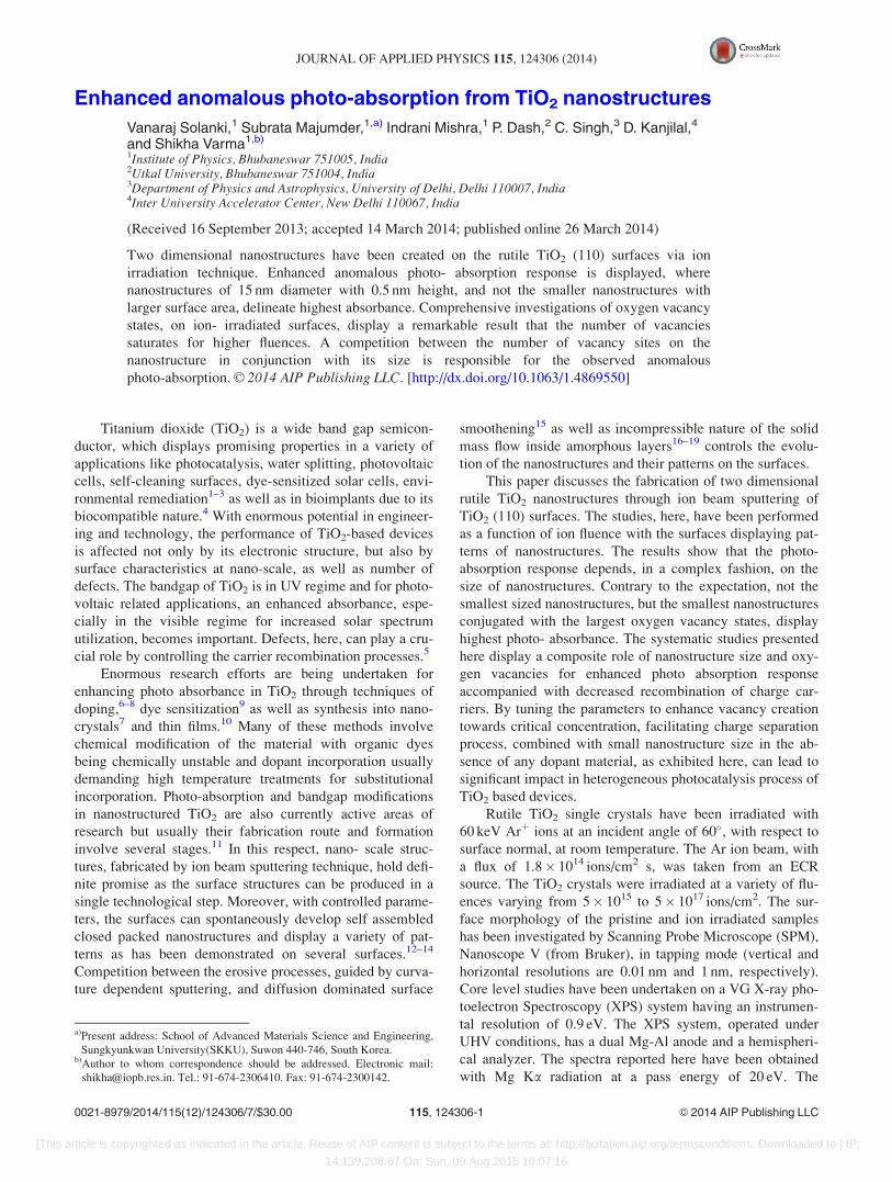
Evolution of the surface morphology of TiO2 (110)
surfaces, after ion irradiation, is displayed in Fig. 1.
Although the pristine sample displays a smooth surface mor-
phology, it gets decorated with a large density (�30
� 1011 cm�2) of 2-dimensional nanostructures, having diam-
eter of �5 nm and height of �0.15 nm, after an irradiation
with a fluence of 5� 1015 ions/cm2 (see Fig. 1(b)). At this
stage, there are no visible correlations among the nanostruc-
tures. For crystalline substrates, the main effect of the ion
impact is to produce adatom and vacancy clusters.20 At
higher fluences (Figs. 1(c) and 1(d)), growth of nanostruc-
tures and formation of clusters of nanostructures along with
the development of some wave like ripple patterns are
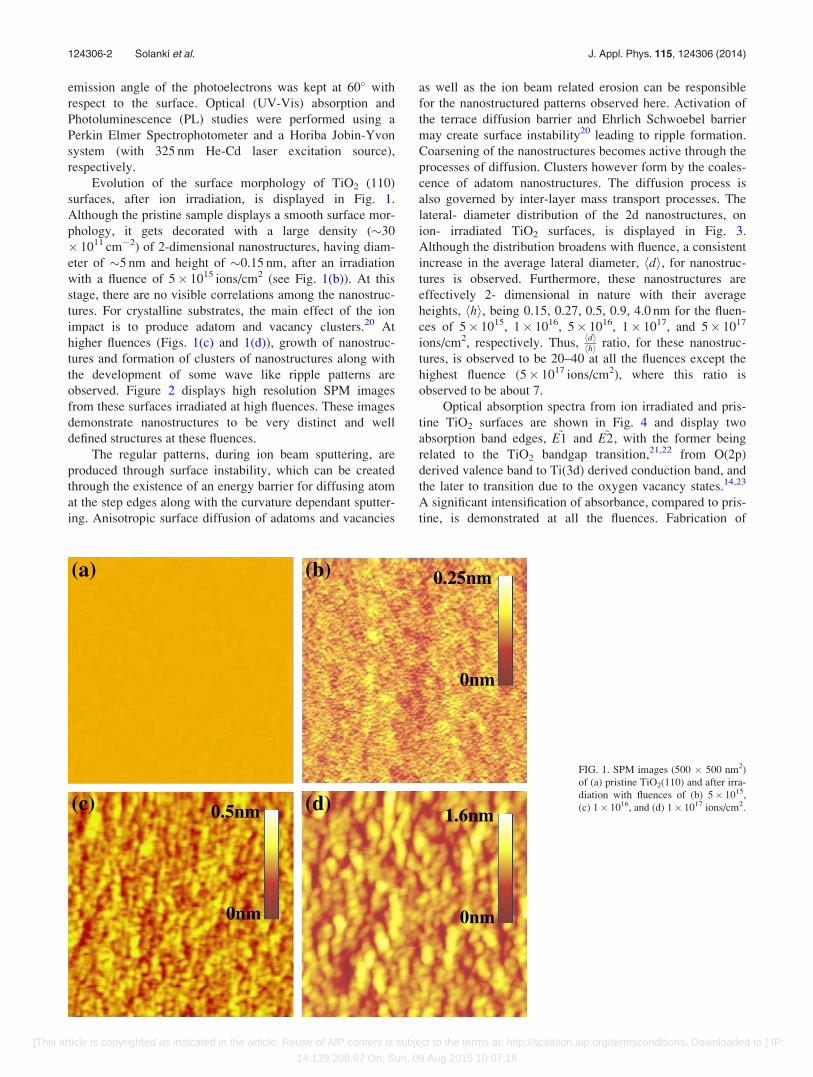
observed. Figure 2 displays high resolution SPM images
from these surfaces irradiated at high fluences. These images
demonstrate nanostructures to be very distinct and well
defined structures at these fluences.
The regular patterns, during ion beam sputtering, are
produced through surface instability, which can be created
through the existence of an energy barrier for diffusing atom
at the step edges along with the curvature dependant sputter-
ing. Anisotropic surface diffusion of adatoms and vacancies
as well as the ion beam related erosion can be responsible
for the nanostructured patterns observed here. Activation of
the terrace diffusion barrier and Ehrlich Schwoebel barrier
may create surface instability20 leading to ripple formation.
Coarsening of the nanostructures becomes active through the
processes of diffusion. Clusters however form by the coales-
cence of adatom nanostructures. The diffusion process is
also governed by inter-layer mass transport processes. The
lateral- diameter distribution of the 2d nanostructures, on
ion- irradiated TiO2 surfaces, is displayed in Fig. 3.
Although the distribution broadens with fluence, a consistent
increase in the average lateral diameter, hdi, for nanostruc-
tures is observed. Furthermore, these nanostructures are
effectively 2- dimensional in nature with their average
heights, hhi, being 0.15, 0.27, 0.5, 0.9, 4.0 nm for the fluen-
ces of 5� 1015, 1� 1016, 5� 1016, 1� 1017, and 5� 1017
ions/cm2, respectively. Thus,hdihhi ratio, for these nanostruc-
tures, is observed to be 20–40 at all the fluences except the
highest fluence (5� 1017 ions/cm2), where this ratio is
observed to be about 7.
Optical absorption spectra from ion irradiated and pris-
tine TiO2 surfaces are shown in Fig. 4 and display two
absorption band edges, ~E1 and ~E2, with the former being
related to the TiO2 bandgap transition,21,22 from O(2p)
derived valence band to Ti(3d) derived conduction band, and
the later to transition due to the oxygen vacancy states.14,23
A significant intensification of absorbance, compared to pris-
tine, is demonstrated at all the fluences. Fabrication of
FIG. 1. SPM images (500 � 500 nm2)
of (a) pristine TiO2(110) and after irra-
diation with fluences of (b) 5� 1015,
(c) 1� 1016, and (d) 1� 1017 ions/cm2.
124306-2 Solanki et al. J. Appl. Phys. 115, 124306 (2014)
[This article is copyrighted as indicated in the article. Reuse of AIP content is subject to the terms at: http://scitation.aip.org/termsconditions. Downloaded to ] IP:
14.139.208.67 On: Sun, 09 Aug 2015 10:07:16
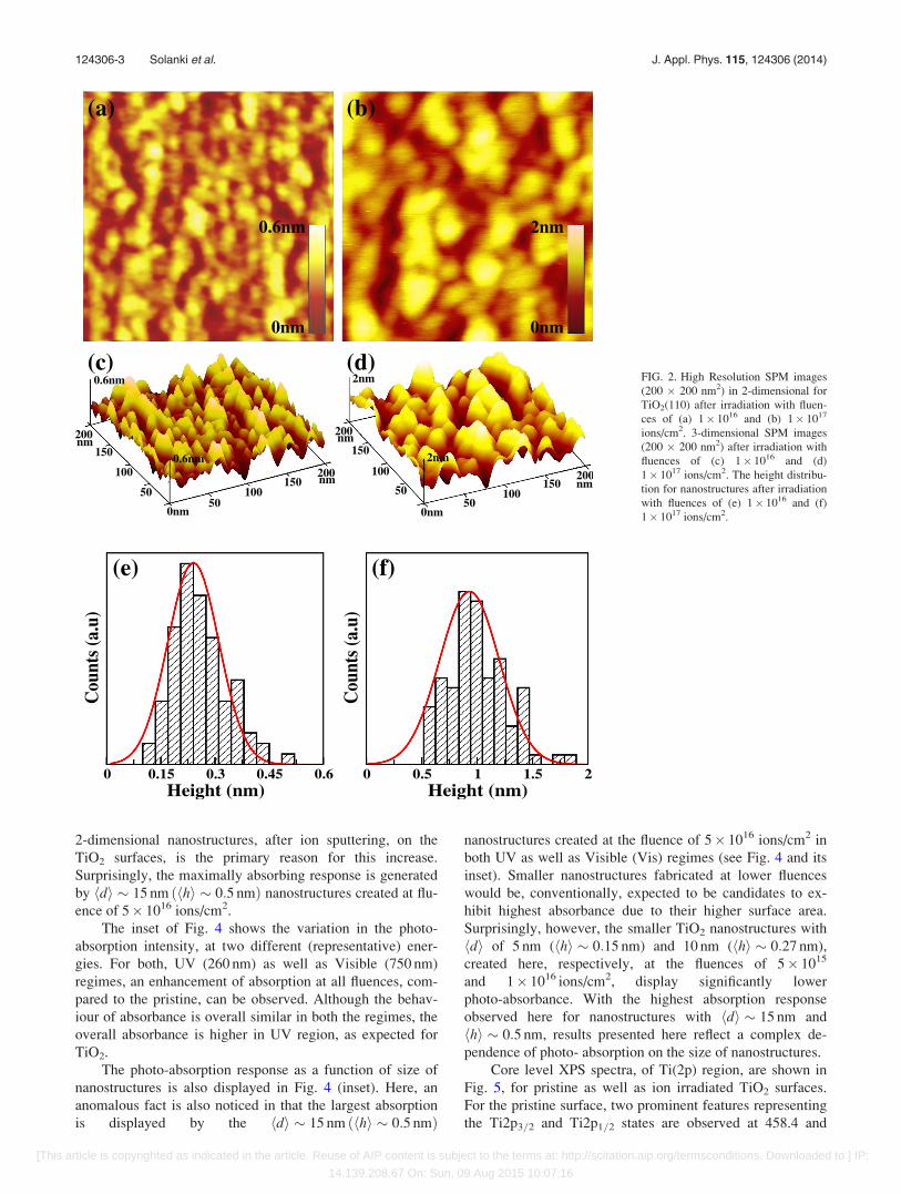
2-dimensional nanostructures, after ion sputtering, on the
TiO2 surfaces, is the primary reason for this increase.
Surprisingly, the maximally absorbing response is generated
by hdi � 15 nm ðhhi � 0:5 nmÞ nanostructures created at flu-
ence of 5� 1016 ions/cm2.
The inset of Fig. 4 shows the variation in the photo-
absorption intensity, at two different (representative) ener-
gies. For both, UV (260 nm) as well as Visible (750 nm)
regimes, an enhancement of absorption at all fluences, com-
pared to the pristine, can be observed. Although the behav-
iour of absorbance is overall similar in both the regimes, the
overall absorbance is higher in UV region, as expected for
TiO2.
The photo-absorption response as a function of size of
nanostructures is also displayed in Fig. 4 (inset). Here, an
anomalous fact is also noticed in that the largest absorption
is displayed by the hdi � 15 nm ðhhi � 0:5 nmÞ
nanostructures created at the fluence of 5� 1016 ions/cm2 in
both UV as well as Visible (Vis) regimes (see Fig. 4 and its
inset). Smaller nanostructures fabricated at lower fluences
would be, conventionally, expected to be candidates to ex-
hibit highest absorbance due to their higher surface area.
Surprisingly, however, the smaller TiO2 nanostructures with
hdi of 5 nm (hhi � 0:15 nm) and 10 nm (hhi � 0:27 nm),
created here, respectively, at the fluences of 5� 1015
and 1� 1016 ions/cm2, display significantly lower
photo-absorbance. With the highest absorption response
observed here for nanostructures with hdi � 15 nm and
hhi � 0:5 nm, results presented here reflect a complex de-
pendence of photo- absorption on the size of nanostructures.
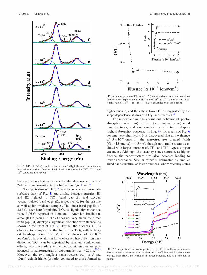
Core level XPS spectra, of Ti(2p) region, are shown in
Fig. 5, for pristine as well as ion irradiated TiO2 surfaces.
For the pristine surface, two prominent features representing
the Ti2p3=2 and Ti2p1=2 states are observed at 458.4 and
FIG. 2. High Resolution SPM images
(200 � 200 nm2) in 2-dimensional for
TiO2(110) after irradiation with fluen-
ces of (a) 1� 1016 and (b) 1� 1017
ions/cm2. 3-dimensional SPM images
(200 � 200 nm2) after irradiation with
fluences of (c) 1� 1016 and (d)
1� 1017 ions/cm2. The height distribu-
tion for nanostructures after irradiation
with fluences of (e) 1� 1016 and (f)
1� 1017 ions/cm2.
124306-3 Solanki et al. J. Appl. Phys. 115, 124306 (2014)
[This article is copyrighted as indicated in the article. Reuse of AIP content is subject to the terms at: http://scitation.aip.org/termsconditions. Downloaded to ] IP:
14.139.208.67 On: Sun, 09 Aug 2015 10:07:16
464.1 eV, respectively (Fig. 5(a)). Both these components
are associated with the Ti4þ state of the pristine sample. In
the lower binding energy regions of each of these features,
two very weak Ti3þ and Ti2þ components, representing the
existence of very small traces of oxygen vacancies on the
pristine TiO2 surface, are observed (see Fig. 5(a)). The inten-
sities of both these features, Ti3þ and Ti2þ, however become
appreciable at higher fluences, suggesting creation of signifi-
cant oxygen vacancies with the formation of species like
Ti2O3 and TiO.24,25
The ion sputtering of the multi-component surface, as
discussed in our earlier studies,4,14,26 can cause preferential
sputtering of TiO2 surface and formation of oxygen vacancy,
with the two associated electrons getting transferred to the
empty 3d orbitals of the neighboring Ti atom forming two
Ti3þ sites. Ti-rich zones, thus formed, can promote nuclea-
tion of self assembled nanodots; in a fashion similar to the
scenario presented for the creation of In -rich nano clusters
on InP surfaces after ion irradiation.12,27 Photoelectron
intensity in XPS exhibits an exponentially decaying behav-
iour as a function of depth and for the kinetic energies of
relevance, here, the mean free path for the photo-electrons
(probing depth) is about 1 nm. With hhi of nanostructures
being �1 nm for most of the fluences, XPS results here can
be attributed to be from the nanostructures. For the tallest 2d
nanostructure (hhi � 4 nm) created at the fluence of 5� 1017
ions/cm2, also, the XPS signal is predominantly from the
nanostructure.
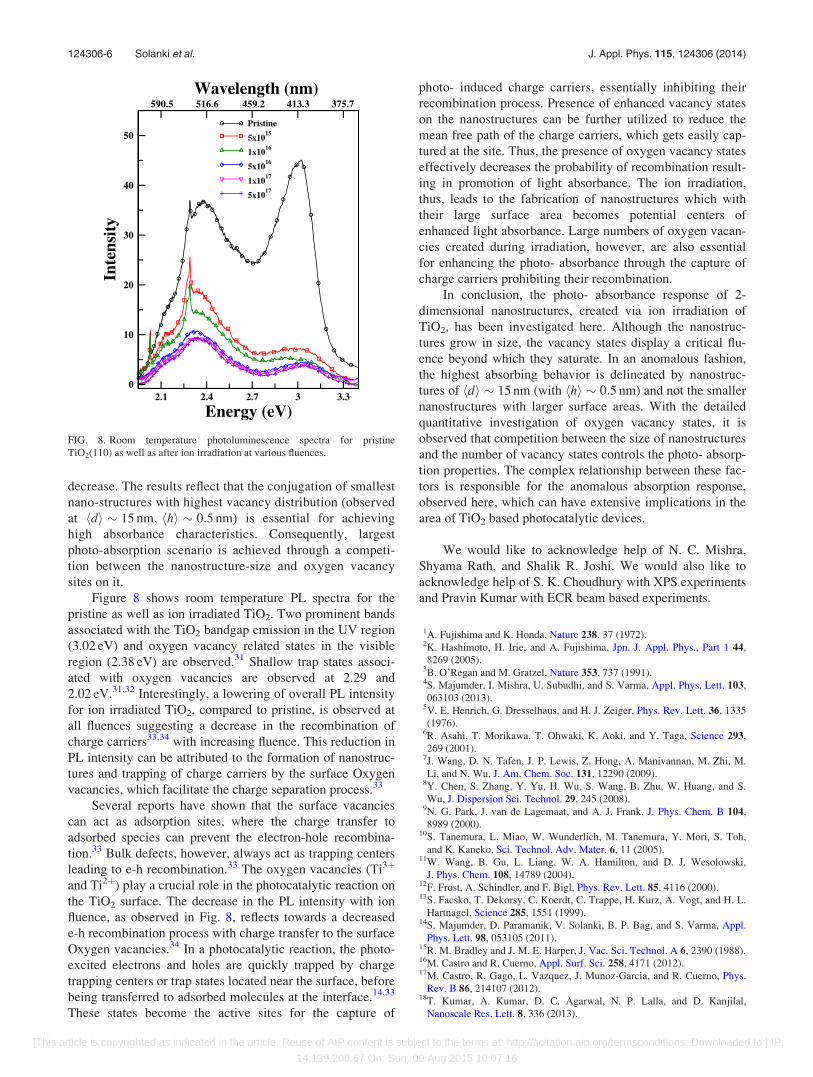
Figure 6 displays the ratio of the total oxygen to Ti spe-
cies on the pristine as well as ion irradiated TiO2 surfaces. A
drastic decrease in the (O/Ti) ratio up to the fluence of
5� 1016 ions/cm2 is accompanied by a saturation at higher
fluences. Remarkably, during this saturation regime, the nano-
structures are continuing to grow (Figs. 1–3). This growth,
however, is not accompanied by any further creation of oxy-
gen vacancies (Ti3þ), which appear to also saturate at
5� 1016 ions/cm2. The inset of Fig. 6 displays the ratio of
intensities of Ti3þ to Ti4þ states (using results of Fig. 5); as
well as the ratio of combined oxygen vacancy states, Ti3þ and
Ti2þ, to Ti4þ as a function of ion fluence. Interestingly, a dras-
tic increase, in both these ratios, is observed up to the fluence
of 5� 1016 ions/cm2 but a saturation beyond that. Once satu-
ration occurs, surfaces consist of nearly 40% oxygen vacan-
cies (Ti3þ, Ti2þ) with 30% of them being Ti3þ type states
(inset Fig. 6). The present study is the first study that investi-
gates the behavior of the vacancy (Ti3þ and Ti2þ) states as a
function of ion fluence. Remarkably, the saturation of vacancy
states, at high fluences (as seen in Fig. 6), is a very interesting
result, which provides a critical limit for enhancing the photo-
catalytic activity of ion sputtered materials. Furthermore, the
results display that ion irradiation, of the TiO2, promotes the
formation of Ti rich zones on the surface, as depicted by lower
than pristine O/Ti ratios. These Ti-rich regions essentially
FIG. 4. UV-Vis absorption spectra are shown for pristine TiO2(110) as well
as after its irradiation at various fluences. Inset shows the photo- absorbance
measured at two specific wavelengths, in UV (260 nm) regime (�) and
Visible (750 nm) regime (�), as a function of ion fluence (bottom scale) as
well as nanostructure size (top scale).
FIG. 3. The lateral diameter distribution of 2-dimensional nanostructures on
TiO2(110) surfaces after irradiation at various fluences. Mean lateral diame-
ter, hdi, of nanostructures and respective fluences is indicated.
124306-4 Solanki et al. J. Appl. Phys. 115, 124306 (2014)
[This article is copyrighted as indicated in the article. Reuse of AIP content is subject to the terms at: http://scitation.aip.org/termsconditions. Downloaded to ] IP:
14.139.208.67 On: Sun, 09 Aug 2015 10:07:16
become the nucleation centers for the development of the
2-dimensional nanostructures observed in Figs. 1 and 2.
Tauc plots shown in Fig. 7, have been generated using ab-
sorbance data (of Fig. 4) and display bandgap energies, E1
and E2 (related to TiO2 band gap ~E1 and oxygen
vacancy-related band edge ~E2, respectively), for the pristine
as well as ion irradiated samples. The direct band gap E1 of
3.18 eV, seen here for pristine TiO2, is slightly higher than the
value 3.06 eV reported in literature.22 After ion irradiation,
although E2 (seen at 2.91 eV) does not vary much, the direct
band gap (E1) displays a significant variation with fluence (as
shown in the inset of Fig. 7). For all the fluences, E1, is
observed to be higher than that for pristine TiO2, with the larg-
est bandgap, being 3.30 eV, at the fluence of 5� 1016
ions/cm2. The blue shift in E1 as observed here, after ion irra-
diation of TiO2, can be explained by quantum confinement
effects, which according to thermodynamic studies are pro-
nounced for nanostructures of sizes smaller than �27 nm.28,29
Moreover, the two smallest nanostructures (hdi of 5 and
10 nm) exhibit higherhdihhi ratio, compared to those formed at
higher fluence, and thus show lower E1 as suggested by the
shape dependence studies of TiO2 nanostructures.30
For understanding the anomalous behavior of photo-
absorption, where hdi � 15 nm (with hhi � 0:5 nm) sized
nanostructures, and not smaller nanostructures, display
highest absorption response (in Fig. 4), the results of Fig. 6
become very significant. It is discovered that at the fluence
of 5� 1016 ions/cm2, the nanostructures created (with
hdi � 15 nm; hhi � 0:5 nm), though not smallest, are asso-
ciated with largest number of, Ti3þ and Ti2þ types, oxygen
vacancies. Although the vacancy states saturate, at higher
fluence, the nanostructure size also increases leading to
lower absorbance. Similar effect is delineated by smaller
sized nanostructure, at lower fluences, where vacancy statesFIG. 5. XPS of Ti(2p) core level for pristine TiO2(110) as well as after ion
irradiation at various fluences. Peak fitted components for Ti4þ, Ti3þ, and
Ti2þ states are also shown.
FIG. 6. Intensity ratio of O(2p) to Ti(2p) states is shown as a function of ion
fluence. Inset displays the intensity ratio of Ti3þ to Ti4þ states as well as in-
tensity ratio of Ti3þ þ Ti2þ to Ti4þ states as a function of ion fluence.
FIG. 7. Tauc plots are shown for pristine TiO2(110) as well as after ion irra-
diation at various fluences. a is the absorption coefficient and E is the photon
energy. Inset shows the variation in direct bandgap, E1, as a function of
fluence.
124306-5 Solanki et al. J. Appl. Phys. 115, 124306 (2014)
[This article is copyrighted as indicated in the article. Reuse of AIP content is subject to the terms at: http://scitation.aip.org/termsconditions. Downloaded to ] IP:
14.139.208.67 On: Sun, 09 Aug 2015 10:07:16
decrease. The results reflect that the conjugation of smallest
nano-structures with highest vacancy distribution (observed
at hdi � 15 nm; hhi � 0:5 nm) is essential for achieving
high absorbance characteristics. Consequently, largest
photo-absorption scenario is achieved through a competi-
tion between the nanostructure-size and oxygen vacancy
sites on it.
Figure 8 shows room temperature PL spectra for the
pristine as well as ion irradiated TiO2. Two prominent bands
associated with the TiO2 bandgap emission in the UV region
(3.02 eV) and oxygen vacancy related states in the visible
region (2.38 eV) are observed.31 Shallow trap states associ-
ated with oxygen vacancies are observed at 2.29 and
2.02 eV.31,32 Interestingly, a lowering of overall PL intensity
for ion irradiated TiO2, compared to pristine, is observed at
all fluences suggesting a decrease in the recombination of
charge carriers33,34 with increasing fluence. This reduction in
PL intensity can be attributed to the formation of nanostruc-
tures and trapping of charge carriers by the surface Oxygen
vacancies, which facilitate the charge separation process.33
Several reports have shown that the surface vacancies
can act as adsorption sites, where the charge transfer to
adsorbed species can prevent the electron-hole recombina-
tion.33 Bulk defects, however, always act as trapping centers
leading to e-h recombination.33 The oxygen vacancies (Ti3þ
and Ti2þ) play a crucial role in the photocatalytic reaction on
the TiO2 surface. The decrease in the PL intensity with ion
fluence, as observed in Fig. 8, reflects towards a decreased
e-h recombination process with charge transfer to the surface
Oxygen vacancies.34 In a photocatalytic reaction, the photo-
excited electrons and holes are quickly trapped by charge
trapping centers or trap states located near the surface, before
being transferred to adsorbed molecules at the interface.14,33
These states become the active sites for the capture of
photo- induced charge carriers, essentially inhibiting their
recombination process. Presence of enhanced vacancy states
on the nanostructures can be further utilized to reduce the
mean free path of the charge carriers, which gets easily cap-
tured at the site. Thus, the presence of oxygen vacancy states
effectively decreases the probability of recombination result-
ing in promotion of light absorbance. The ion irradiation,
thus, leads to the fabrication of nanostructures which with
their large surface area becomes potential centers of
enhanced light absorbance. Large numbers of oxygen vacan-
cies created during irradiation, however, are also essential
for enhancing the photo- absorbance through the capture of
charge carriers prohibiting their recombination.
In conclusion, the photo- absorbance response of 2-
dimensional nanostructures, created via ion irradiation of
TiO2, has been investigated here. Although the nanostruc-
tures grow in size, the vacancy states display a critical flu-
ence beyond which they saturate. In an anomalous fashion,
the highest absorbing behavior is delineated by nanostruc-
tures of hdi � 15 nm (with hhi � 0:5 nm) and not the smaller
nanostructures with larger surface areas. With the detailed
quantitative investigation of oxygen vacancy states, it is
observed that competition between the size of nanostructures
and the number of vacancy states controls the photo- absorp-
tion properties. The complex relationship between these fac-
tors is responsible for the anomalous absorption response,
observed here, which can have extensive implications in the
area of TiO2 based photocatalytic devices.
We would like to acknowledge help of N. C. Mishra,
Shyama Rath, and Shalik R. Joshi. We would also like to
acknowledge help of S. K. Choudhury with XPS experiments
and Pravin Kumar with ECR beam based experiments.
1A. Fujishima and K. Honda, Nature 238, 37 (1972).2K. Hashimoto, H. Irie, and A. Fujishima, Jpn. J. Appl. Phys., Part 1 44,
8269 (2005).3B. O’Regan and M. Gratzel, Nature 353, 737 (1991).4S. Majumder, I. Mishra, U. Subudhi, and S. Varma, Appl. Phys. Lett. 103,
063103 (2013).5V. E. Henrich, G. Dresselhaus, and H. J. Zeiger, Phys. Rev. Lett. 36, 1335
(1976).6R. Asahi, T. Morikawa, T. Ohwaki, K. Aoki, and Y. Taga, Science 293,
269 (2001).7J. Wang, D. N. Tafen, J. P. Lewis, Z. Hong, A. Manivannan, M. Zhi, M.
Li, and N. Wu, J. Am. Chem. Soc. 131, 12290 (2009).8Y. Chen, S. Zhang, Y. Yu, H. Wu, S. Wang, B. Zhu, W. Huang, and S.
Wu, J. Dispersion Sci. Technol. 29, 245 (2008).9N. G. Park, J. van de Lagemaat, and A. J. Frank, J. Phys. Chem. B 104,
8989 (2000).10S. Tanemura, L. Miao, W. Wunderlich, M. Tanemura, Y. Mori, S. Toh,
and K. Kaneko, Sci. Technol. Adv. Mater. 6, 11 (2005).11W. Wang, B. Gu, L. Liang, W. A. Hamilton, and D. J. Wesolowski,
J. Phys. Chem. 108, 14789 (2004).12F. Frost, A. Schindler, and F. Bigl, Phys. Rev. Lett. 85, 4116 (2000).13S. Facsko, T. Dekorsy, C. Koerdt, C. Trappe, H. Kurz, A. Vogt, and H. L.
Hartnagel, Science 285, 1551 (1999).14S. Majumder, D. Paramanik, V. Solanki, B. P. Bag, and S. Varma, Appl.
Phys. Lett. 98, 053105 (2011).15R. M. Bradley and J. M. E. Harper, J. Vac. Sci. Technol. A 6, 2390 (1988).16M. Castro and R. Cuerno, Appl. Surf. Sci. 258, 4171 (2012).17M. Castro, R. Gago, L. Vazquez, J. Munoz-Garcia, and R. Cuerno, Phys.
Rev. B 86, 214107 (2012).18T. Kumar, A. Kumar, D. C. Agarwal, N. P. Lalla, and D. Kanjilal,
Nanoscale Res. Lett. 8, 336 (2013).
FIG. 8. Room temperature photoluminescence spectra for pristine
TiO2(110) as well as after ion irradiation at various fluences.
124306-6 Solanki et al. J. Appl. Phys. 115, 124306 (2014)
[This article is copyrighted as indicated in the article. Reuse of AIP content is subject to the terms at: http://scitation.aip.org/termsconditions. Downloaded to ] IP:
14.139.208.67 On: Sun, 09 Aug 2015 10:07:16

19T. Kumar, A. Kumar, N. Lalla, S. Hooda, S. Ojha, S. Verma, and D.
Kanjilal, Appl. Surf. Sci. 283, 417 (2013).20U. Valbusa, C. Boragno, and F. Buatier de Mongeot, J. Phys. Condens.
Mater. 14, 8153 (2002).21A. K. Rumaiz, J. C. Woicik, E. Cockayne, H. Y. Lin, G. H. Jaffari, and
S. I. Shah, Appl. Phys. Lett. 95, 262111 (2009).22J. Pascual, J. Camassel, and H. Mathieu, Phys. Rev. B 18, 5606
(1978).23B. Santara, P. K. Giri, K. Imakita, and M. Fujii, J. Phys. Chem. C 117,
23402 (2013).24S. D. Yoon, Y. Chen, A. Yang, T. L. Goodrich, X. Zuo, D. A. Arena, K.
Ziemer, C. Vittoria, and V. G. Harris, J. Phys. Condens. Mater. 18, L355
(2006).25H. Y. Jeong, J. Y. Lee, S. Y. Choi, and J. W. Kim, Appl. Phys. Lett. 95,
162108 (2009).26S. Majumder, D. Paramanik, V. Solanki, I. Mishra, D. K. Avasthi, D.
Kanjilal, and S. Varma, Appl. Surf. Sci. 258, 4122 (2012); V. Solanki, S.
Majumder, I. Mishra, S. R. Joshi, D. Kanjilal, and S. Varma, Radiat. Eff.
Defects Solids 168, 518 (2013).27D. Paramanik, S. N. Sahu, and S. Varma, J. Phys. D: Appl. Phys. 41,
125308 (2008).28N. Satoh, T. Nakashima, K. Kamikura, and K. Yamamoto, Nat.
Nanotechnol. 3, 106 (2008).29H. Peng and J. Li, J. Phys. Chem. C 112, 20241 (2008).30G. Guisbiers, O. V. Overschelde, and M. Wautelet, Appl. Phys. Lett. 92,
103121 (2008).31M. Yang, W. Liu, J. L. Sun, and J. L. Zhu, Appl. Phys. Lett. 100, 043106
(2012).32C. Fabrega, T. Andreu, F. Guell, J. D. Prades, S. Estrade, J. M. Rebled, F.
Peiro, and J. R. Morante, Nanotechnology 22, 235403 (2011).33X. Pan, M. Q. Yang, X. Fu, N. Zhang, and Y. J. Xu, Nanoscale 5, 3601
(2013).34M. Luo, K. Cheng, W. Weng, C. Song, P. Du, G. Shen, G. Xu, and G.
Han, J. Phys. D: Appl. Phys. 42, 105414 (2009).
124306-7 Solanki et al. J. Appl. Phys. 115, 124306 (2014)
[This article is copyrighted as indicated in the article. Reuse of AIP content is subject to the terms at: http://scitation.aip.org/termsconditions. Downloaded to ] IP:
14.139.208.67 On: Sun, 09 Aug 2015 10:07:16