Available online at www.sciencedirect.com ScienceDirect Energy Procedia 00 (2015) 000–000 www.elsevier.com/locate/procedia 1876-6102 © 2015 The Authors. Published by Elsevier Ltd. Peer-review under responsibility of Gunnar Schubert, Guy Beaucarne and Jaap Hoornstra. 5th Workshop on Metallization of Crystalline Silicon Solar Cells Dispensing Technology on the Route to an Industrial Metallization Process Maximilian Pospischil a *, Martin Kuchler a , Markus Klawitter a , Carlos Rodríguez a , Milan Padilla a , Raphael Efinger a , Michael Linse a , Angel Padilla a , Harald Gentischer a , Markus König b , Matthias Hörteis b , Lars Wende c , Oliver Doll d , Roland Zengerle e , Florian Clement a and Daniel Biro a a Fraunhofer Institute for Solar Energy Systems (ISE), Heidenhofstr. 2, D-79110 Freiburg, Germany b Heraeus Precious Metals GmbH & Co. KG, Electronic Materials Division, Business Unit Photovoltaics, Heraeusstr. 12-14, D-63450 Hanau, Germany c ASYS Automatisierungssysteme GmbH, Solar & New Technologies, Benzstr. 10, D-89160 Dornstadt, Germany d Merck KGaA, Performance Materials Division, Postcode Q004/001, Frankfurter Str. 250, D-64293 Darmstadt, Germany e Department of Microsystems Engineering – IMTEK, University of Freiburg, Georges-Köhler-Allee 103, D-79110 Freiburg, Germany Abstract This study presents a new developed, inline applicable dispensing platform that is equipped with an advanced version of previously introduced parallel dispensing print heads and works as drop-in-replacement in existing manufacturing lines. At process speeds of up to 700 mm•s-1 and a substantially improved process stability, the impact of the resulting contact geometries on optical and ohmic losses was analysed in detail. A reduced finger width as well as an effective width of just 48% after encapsulation of the finger width leads to nearly 50% reduction of shading losses compared to screen printed samples. A substantially improved finger homogeneity leads to similar grid resistances at 20% less silver consumption. Consequently, recent cell results on industrial emitters (R sh = 90 Ω/sq.) showed an efficiency increase of up to +0.4%abs. in comparison to standard single screen printing reaching top values of η = 20.5% on PERC structures. A key improvement of the technology is the new ability to process certain metal pastes originally designed for screen printing applications and thus keep in track with fast emerging paste development. Successfully evaluated screen printing pastes then can be rheologically adapted in order to reach ultrafine contact fingers at high aspect ratios and extract the whole advantage of this non-contacting printing technology. © 2014 The Authors. Published by Elsevier Ltd. Peer-review under responsibility of the scientific committee of the SiliconPV 2014 conference. * Corresponding author. Tel.: +49 761 4588 5268 E-mail address: [email protected]

Welcome message from author
This document is posted to help you gain knowledge. Please leave a comment to let me know what you think about it! Share it to your friends and learn new things together.
Transcript

Available online at www.sciencedirect.com
ScienceDirect Energy Procedia 00 (2015) 000–000
www.elsevier.com/locate/procedia
1876-6102 © 2015 The Authors. Published by Elsevier Ltd. Peer-review under responsibility of Gunnar Schubert, Guy Beaucarne and Jaap Hoornstra.
5th Workshop on Metallization of Crystalline Silicon Solar Cells
Dispensing Technology on the Route to an Industrial Metallization Process
Maximilian Pospischila*, Martin Kuchlera, Markus Klawittera, Carlos Rodrígueza, Milan Padillaa, Raphael Efingera, Michael Linsea, Angel Padillaa, Harald Gentischera,
Markus Königb, Matthias Hörteisb, Lars Wendec, Oliver Dolld, Roland Zengerlee, Florian Clementa and Daniel Biroa
aFraunhofer Institute for Solar Energy Systems (ISE), Heidenhofstr. 2, D-79110 Freiburg, Germany bHeraeus Precious Metals GmbH & Co. KG, Electronic Materials Division, Business Unit Photovoltaics, Heraeusstr. 12-14, D-63450 Hanau,
Germany cASYS Automatisierungssysteme GmbH, Solar & New Technologies, Benzstr. 10, D-89160 Dornstadt, Germany
dMerck KGaA, Performance Materials Division, Postcode Q004/001, Frankfurter Str. 250, D-64293 Darmstadt, Germany eDepartment of Microsystems Engineering – IMTEK, University of Freiburg, Georges-Köhler-Allee 103, D-79110 Freiburg, Germany
Abstract
This study presents a new developed, inline applicable dispensing platform that is equipped with an advanced version of previously introduced parallel dispensing print heads and works as drop-in-replacement in existing manufacturing lines. At process speeds of up to 700 mm•s-1 and a substantially improved process stability, the impact of the resulting contact geometries on optical and ohmic losses was analysed in detail. A reduced finger width as well as an effective width of just 48% after encapsulation of the finger width leads to nearly 50% reduction of shading losses compared to screen printed samples. A substantially improved finger homogeneity leads to similar grid resistances at 20% less silver consumption. Consequently, recent cell results on industrial emitters (Rsh = 90 Ω/sq.) showed an efficiency increase of up to +0.4%abs. in comparison to standard single screen printing reaching top values of η = 20.5% on PERC structures. A key improvement of the technology is the new ability to process certain metal pastes originally designed for screen printing applications and thus keep in track with fast emerging paste development. Successfully evaluated screen printing pastes then can be rheologically adapted in order to reach ultrafine contact fingers at high aspect ratios and extract the whole advantage of this non-contacting printing technology. © 2014 The Authors. Published by Elsevier Ltd. Peer-review under responsibility of the scientific committee of the SiliconPV 2014 conference.
* Corresponding author. Tel.: +49 761 4588 5268
E-mail address: [email protected]

2 Pospischil et al. / Energy Procedia 00 (2015) 000–000
Keywords: silicon, solar cells, printing, metallization, dispensing, contact geometries, economic evaluation, analytic simulation
1. Introduction
Silicon solar cell metallization is still dominated by screen printing technology offering a robust contact formation and proven long term stability. Forced by a rapid decline of retail module prices, Ag-paste consumption had to be substantially reduced [1]. Consequently, paste and process development were pushed to achieve printed line widths of less than 50µm. However, known issues like mesh marks, line spreading or screen wear have not yet overcome. Different thick film technologies like stencil printing [2] or recently introduced co-extrusion approach [3] are promising technologies but are challenged by high consumable costs in the former or the competition of fast emerging screen printing pastes that cannot be directly used in the latter approach. The dispensing technology, as described by Specht et al. [4], offers a contactless, high-throughput single-step metallization process significantly reducing finger width and thus shading losses. Record cell efficiencies of 20.6% on 125x125mm² FZ p-type material using dispensing technology on MWT-PERC (Metal Wrap Through – Passivated Emitter and Rear Cell) solar cells, featuring a selective emitter structure were presented by Lohmüller et al. [5]. Dispensing pastes are directly derived from screen printing paste development [6] and resulting finger geometries can be varied in a wide range by adapting paste rheology as described in previous studies e.g. [7]. In order to demonstrate the benefit of these advantages, the analytical 2D simulative tool Gridmaster [8] was enhanced to observe the effect of various geometrical parameters on solar cell results and manufacturing costs [9]. Both however, imply a stable metallization process at high throughput rates. For this reason, a novel dispensing platform was developed, providing fully automated inline production feasibility. In the following, this platform, was equipped with an advanced parallel dispensing print head as introduced in [10] and applied for extensive solar cell processing. Here, a focus was put on process stability using latest industrially manufactured dispensing pastes with sufficient contacting behavior on state of the art emitters (Rsh > 90 Ω/sq.).
Nomenclature
Af (µm²) finger cross-section area Rsh (Ω/sq.) Emitter sheet resistance D (µm) nozzle outlet diameter Voc (mV) open circuit voltage EW (%) relative effective finger width wBB (µm) busbar width FF (%) fill factor wc(µm) contact width jsc (mA/cm²) short circuit current weff (µm) absolute effective finger width N (-) Number of contact fingers wo (µm) optical (= max.) finger width
rBulk (Ω∙cm) bulk resistivity ws(µm) screen opening width for single and double screen printed reference samples
rf (µ Ω∙cm) finger resistivity ρc (mΩ∙cm²) contact resistivity RGrid (Ω/m) finger grid resistivity (%) solar cell conversion efficiency
2. Approach
The focus of three years lasting research project “GECKO” was mainly the development of dispensing technology aiming on an industrial implementation. Here, precise rheological analysis of dispensing pastes [7, 10] and a subsequent implementation of a rheological paste model allowed for an efficient development of parallel print heads by computational fluid dynamic (CFD) simulations [10, 11].
After providing a homogeneous mass flow distribution to all nozzles and optimizing the shape of the incorporated nozzle plates, record finger widths of just 27µm were demonstrated using previous paste generations [10]. During this study, development was focused on providing high process stability with new developed silver
pastethe pprep
R
resudeterwas modHereeffec
3. R
3.1.
Drangcan cont
Hmatebringtransapplaspehighredu
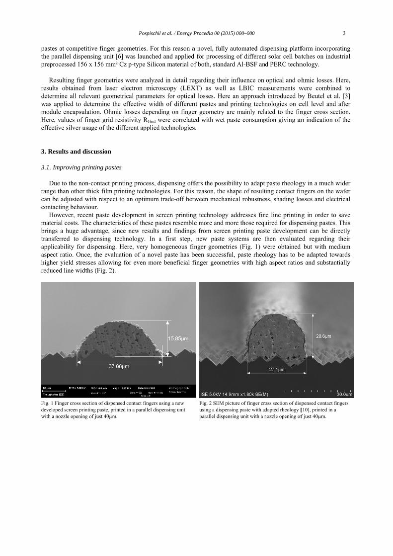
Fig. 1develwith a
es at competitparallel dispenprocessed 156
Resulting fingelts obtained rmine all releapplied to de
dule encapsulae, values of fictive silver us
Results and di
Improving pr
Due to the nonge than other tbe adjusted w
tacting behaviHowever, receerial costs. Thgs a huge advsferred to dilicability for dect ratio. Onceher yield stresuced line width
1 Finger cross secloped screen printa nozzle opening
tive finger gensing unit [6] x 156 mm² C
er geometries from laser e
evant geometretermine the ation. Ohmic inger grid resisage of the dif
iscussion
rinting pastes
n-contact printthick film prinwith respect toour.
ent paste devehe characteristvantage, sincespensing techdispensing. He, the evaluatses allowing hs (Fig. 2).
ction of dispensedting paste, printedof just 40µm.
Pospischi
ometries. Forwas launched
Cz p-type Silic
were analyzeelectron microrical parameteeffective widtlosses dependistivity RGrid w
fferent applied
ting process, dnting technoloo an optimum
elopment in stics of these pae new resultshnology. In
Here, very homtion of a novefor even mor
d contact fingers d in a parallel dis
il et al. / Energy P
r this reason ad and applied on material of
ed in detail reoscopy (LEXers for opticalth of differending on fingewere correlated technologies
dispensing offogies. For this
trade-off betw
creen printingastes resemble
s and findingsa first step, mogeneous finel paste has be beneficial f
using a new spensing unit
Procedia 00 (201
a novel, fully d for processinf both, standar
egarding their XT) as well l losses. Herent pastes and er geometry ared with wet ps.
fers the possib reason, the shween mechan
g technology e more and ms from screennew paste s
nger geometrbeen successfufinger geometr
Fig. 2 SEM picusing a dispenparallel dispen
15) 000–000
automated disng of differentrd Al-BSF an
influence on as LBIC me
e an approach printing technre mainly relaaste consump
bility to adapt hape of result
nical robustnes
addresses finmore those requn printing passystems are ties (Fig. 1) wul, paste rheolries with high
cture of finger crosing paste with ad
nsing unit with a n
spensing platft solar cell batd PERC techn
optical and ohasurements wintroduced b
nologies on cated to the finption giving an
paste rheologing contact finss, shading lo
ne line printinuired for dispete developmethen evaluate
were obtained logy has to bh aspect ratios
oss section of dispdapted rheology [nozzle opening of
form incorporatches on indunology.
hmic losses. Hwere combineby Beutel et acell level and nger cross secn indication o
gy in a much wngers on the w
osses and elec
ng in order to ensing pastes.ent can be dired regarding d but with mebe adapted tows and substan
spensed contact fi[10], printed in a f just 40µm.
3
rating ustrial
Here, ed to al. [3]
after ction. of the
wider wafer trical
save This rectly their
edium wards ntially
ingers

4 Pospischil et al. / Energy Procedia 00 (2015) 000–000
3.2. Development of multi nozzle print heads
In order to significantly increase throughput rates during dispensing, a novel parallel print head was developed. For this reason, rheological paste characteristics were used to implement an universal paste model including Non-Newtonian flow patterns like shear thinning and yield stress [10]. After verifying this paste model using a single nozzle dispense setup, the focus was put on the development of a ten nozzle parallel dispensing prototype (Fig. 3). Here, a modular setup allowed for a separate optimization of dispensing nozzles, valves and paste distribution.
In the following, multi nozzle print head designs were tested and optimized regarding their robustness concerning fabrication tolerances. Due to specially designed nozzles, the necessary dispensing pressure was reduced by a factor of up to ten compared to commercial standard nozzles. A central fed paste supply with nozzle pitches of only 1.56 mm was realized which allows for further scalability of the design in the future.
3.3. Integration into an inline applicable platform
Finally, the novel print head was integrated in a newly developed fully automated dispensing platform (Fig. 4) which permits industrial manufacturing sequences with the new setup. Here, a fully automated cell handling system allows for a precise application of dispensed grid structures on industrial solar cells.
Continuous line dispensing at line speeds of more than 700 mm•s-1 was already reached using this setup. Furthermore, a nozzle distance of just 50 µm can be realized during dispensing with this platform. However, rheological adaptions of the dispensing pastes also allow for a stable process at much greater distances by stretching the paste during its free flow phase.
3.4. Concepts for Inline Integration
Most standard back-end production line concepts consist of three subsequent printing steps. Two are needed for the back surfaces, namely printing of Aluminum providing a full area contact of the p-type base and local silver pads that are required for soldered module interconnection. The front side grid is finally printed using a third screen printer which is followed by the fast firing oven (FFO) as visible in Fig. 5, top route. In order to further increase cell efficiencies, various routes with four printers in series have been introduced, mainly dual and double printing. The former allows for a reduction of recombination losses and silver consumption by applying a specially designed, non-contacting busbar paste (i.e. floating busbar concept [12]). Here, contact fingers are alternatively applied by stencil printing. The latter (i.e. double printing or print on print) increases finger aspect ratio (AR) and reduces the influence of mesh marks by adding a second printing step that is precisely aligned to the first one, see Fig. 5, second route.
The integration of the inline dispensing platform states the third route in Fig. 5. Here, a conventional busbar
printing step is followed by the application of the dispensed finger grid before entering the FFO. In opposite to all previous routes, the contact less dispensing step does not require a previous drying step which allows for a further reduction of investment costs and foot print of the tool. With all other back end steps remaining the same, the integration of a dispensing unit can be seen as drop-in-replacement compared to all other dual or double printing approaches. With line speeds of more than 700 mm•s-1, the expected through put of the back-end production line by far is not limited by the dispensing process. Moreover, even a junction of two parallel printing lines into one dispensing unit is possible providing that the print head contains a sufficient number of parallel operating dispensing nozzles.

Fig. 3print the ne
3.5.
Osimicontinflucomproc
Osilvecorresligh
Fig. 6openi
3 Advanced versihead during cell ew dispensing pla
Influence of c
Once, a stable lar electrical
tact finger. Thuences both, sh
mparison, it deccess when appOn the other her consumptioesponding valhtly lower than
6 Optical finger wing width ws and
on of the ten nozmanufacturing watform.
contact finger
dispensing prbehavior the
he optical finghading as welcreases from w
plying a nozzlehand, the resulon, since a colues of the disn those obtain
width (left) wo annozzle opening d
Pospischi
zle within
Fig. 4inlineform
geometry on
rocess at high expected celer width wo isll as recombinwo = 53µm foe plate with oplting finger cronstant numbespensing procned for both re
nd corresponding diameter D, respe
il et al. / Energy P
4 Completely newe applicable dispeat Fraunhofer ISE
cell results
h through put ll and modules directly linkenation losses uor the single spening diametross section Aer of contact esses with noeference techn
finger cross sectictively.
Procedia 00 (201
w developed, ensing plat-E’s PV-TEC.
rates has beee results highed to the correunderneath thecreen printed ter of D = 40µ
Af has a strongfingers was
ozzle plates ofnologies (scree
ion (right) of diff
15) 000–000
Fig. 5 Concepts printing approacroute) is comparroute) and dispe
en establishedhly depend onesponding mee contacts. Foreference to a
µm. g influence onapplied to all
f D = 50µm anen printing an
ferent printing tec
for inline integraches. Standard sinred with dual/douensing (bottom ro
and applied n the geomettal coverage or the three setaround 35µm
n grid resistanl technologiesnd D = 40µm,nd double scre
chnologies with in
ation of different ngle printing (topuble printing (secoute).
metal pastes trical shape oof the cell andtups applied infor the dispen
nce RGrid as ws (N = 100). H, respectively
een printing).
ndicated screen
5
p ond
show of the d thus n this nsing
ell as Here, were

6 Pospischil et al. / Energy Procedia 00 (2015) 000–000
However, another advantage of the dispensing process is its substantially increased finger homogeneity (Fig. 7) that allows to print extremely fine lines without drawbacks coming from mesh marks or paste spreading that both lead to additional silver consumption that does not contribute to lateral current transport within the fingers. In order to illustrate this effect, wet paste consumption of various printing experiments on industrial Cz material with both technologies was plotted against the values of the grid resistance RGrid (Fig. 8) obtained from IV-measurement of the corresponding solar cells.
Fig. 7 Comprison of finger homogeneity of the applied technologies by means of the standard deviation in finger cross section area Af.
Fig. 8 Correlation of wet paste consumption and grid resistance RGrid for dispensing and screen printed solar cells, respectively.
As expected, a linear correlation between paste consumption and RGrid is clearly visible for all dispensed contact fingers with a homogeneous finger cross section Af. All screen printed solar cells however suffer from an increased grid resistance at similar paste consumption that implies that the effective silver usage is reduced by around 20% compared to dispensed finger grids.
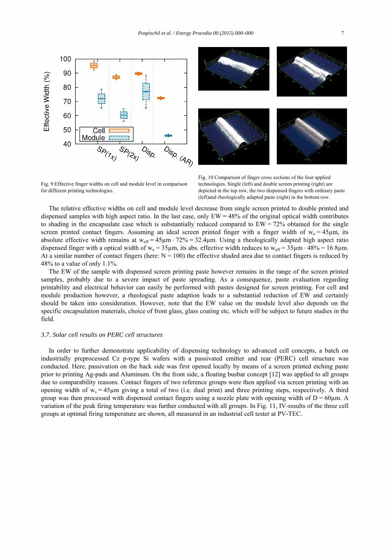
3.6. Influence of finger shape: Determination of effective finger width
To assess the desired optical coupling of light bouncing from a finger back onto the cell surface, we evaluated the relative effective widths (EW) for all compared metallization technologies on a cell and module level. We defined this value as in [13] as the fraction of effective shading and theoretical geometrical shading defined by the optical finger width. Our EW determination method of choice was using spectrally resolved light-beam induced current measurements (SR-LBIC). The measurement and evaluation is similar to the one recently proposed by Beutel et al. [3]. In this work however, the reflectance of surface texture was not regarded as part of the solar cell shading. Furthermore, EW was determined for six wavelengths from 405 nm to 1064 nm to account for spectral dependence over the relevant range. The resulting spectrally dependent EW curve was weighed with the AM 1.5G spectrum as well as the solar cells external quantum efficiency (EQE) for an EW value representative to standard testing conditions. More details on this approach and the uncertainties of other EW determination methods will be discussed elsewhere.
The results of the applied printing technologies can be seen in Fig. 9. Here, single and double screen printing was compared with a sample with dispensed screen printing paste and one with a rheologically optimized dispensing paste with high aspect ratios (AR).
60 80 100 120 140 160
10
20
30
40
50
60
70
80 Dispenser Screen Printed
N = 100
Gri
d R
es (m
)
mwet
(mg)
D = 50µm
D = 40µm
D = 60µm
Pospischil et al. / Energy Procedia 00 (2015) 000–000 7
Fig. 9 Effective finger widths on cell and module level in comparison for different printing technologies.
Fig. 10 Comparison of finger cross sections of the four applied technologies. Single (left) and double screen printing (right) are depicted in the top row, the two dispensed fingers with ordinary paste (left)and rheologically adapted paste (right) in the bottom row.
The relative effective widths on cell and module level decrease from single screen printed to double printed and dispensed samples with high aspect ratio. In the last case, only EW = 48% of the original optical width contributes to shading in the encapsulate case which is substantially reduced compared to EW = 72% obtained for the single screen printed contact fingers. Assuming an ideal screen printed finger with a finger width of wo = 45µm, its absolute effective width remains at weff = 45µm ∙ 72% = 32.4µm. Using a rheologically adapted high aspect ratio dispensed finger with a optical width of wo = 35µm, its abs. effective width reduces to weff = 35µm ∙ 48% = 16.8µm. At a similar number of contact fingers (here: N = 100) the effective shaded area due to contact fingers is reduced by 48% to a value of only 1.1%.
The EW of the sample with dispensed screen printing paste however remains in the range of the screen printed samples, probably due to a severe impact of paste spreading. As a consequence, paste evaluation regarding printability and electrical behavior can easily be performed with pastes designed for screen printing. For cell and module production however, a rheological paste adaption leads to a substantial reduction of EW and certainly should be taken into consideration. However, note that the EW value on the module level also depends on the specific encapsulation materials, choice of front glass, glass coating etc. which will be subject to future studies in the field.
3.7. Solar cell results on PERC cell structures
In order to further demonstrate applicability of dispensing technology to advanced cell concepts, a batch on industrially preprocessed Cz p-type Si wafers with a passivated emitter and rear (PERC) cell structure was conducted. Here, passivation on the back side was first opened locally by means of a screen printed etching paste prior to printing Ag-pads and Aluminum. On the front side, a floating busbar concept [12] was applied to all groups due to comparability reasons. Contact fingers of two reference groups were then applied via screen printing with an opening width of ws = 45µm giving a total of two (i.e. dual print) and three printing steps, respectively. A third group was then processed with dispensed contact fingers using a nozzle plate with opening width of D = 60µm. A variation of the peak firing temperature was further conducted with all groups. In Fig. 11, IV-results of the three cell groups at optimal firing temperature are shown, all measured in an industrial cell tester at PV-TEC.

8 Pospischil et al. / Energy Procedia 00 (2015) 000–000
Fig. 11 IV-results of recent cell batch on industrial pre-processed and passivated Cz p-type material (PERC concept). All groups contain screen printed non-contacting busbars prior to the subsequent application of contact fingers by alternatively one or two additional screen printing steps or dispensing, respectively.
At similar contacting behaviour, the fill factor is strongly influenced by the resulting grid resistance. Consequently, the groups with double printed and dispensed contact fingers show substantially increased FF values than the samples with single screen printed contact fingers. As expected the jsc values of dispensed contact fingers are increased due to substantially lower shading losses and an improved effective width. The Voc is on a reasonably high level for all groups due to the applied PERC concept. The reason for slightly decreasing values in the double printed and the dispensed groups has not yet been completely identified but remains in the per mill range, comparatively. Finally, resulting cell efficiencies surpassed 20% for all groups, hence the concept of the locally opened passivation worked well for all samples. A maximum value of η = 20.5% was reached in the dispensed group giving an efficiency gain of 2%rel. (0.4%abs.) compared to the single screen printed group (here: dual printing) and 1%rel. (0.2%abs.) with respect to the group with double printed contact fingers.
4. Conclusions and outlook
Fast emerging thick film printing technologies remain a dynamic challenge for any kind of alternative metallization technology. The possibility to directly transfer results and findings from screen printing paste development however, allows for the enhancement of dispensing technology towards industrial cell processing.
Dispensed grid lines offer a substantially more homogeneous contact shape that require 20% less silver consumption as screen printed fingers to obtain similar grid resistances. Due to their high aspect ratio and a superior shape, an additional benefit results from a comparison of the two technologies regarding their effective finger width.

Pospischil et al. / Energy Procedia 00 (2015) 000–000 9
Here, an effective width of only 48% of their optical width contributes to shading in the encapsulate case which is substantially reduced compared to 72% obtained for screen printed contact fingers.
Consequently, on industrially preprocessed PERC solar cells, a top value of η = 20.5% was reached with dispensing, giving an efficiency gain of 2%rel. (0.4%abs.) compared to a conventional dual screen printed reference group. With the new developed, inline applicable dispensing platform, a continuous printing process was demonstrated at printing speeds up to 700 mm·s-1. The integrated, advanced version of a ten nozzle parallel dispensing print head can be easily scaled for a future application in cell production.
Acknowledgements
The authors would like to thank all co-workers at the Photovoltaic Technology Evaluation Center (PV-TEC) and the mechanical workshop at Fraunhofer ISE for processing of the samples. This work was supported by the German Federal Ministry for Economic Affairs and Energy within the research project “GECKO” under contract number 0325404.
References
[1] H. Hannebauer et al., Energy Procedia 43, 66 (2013). [2] B. Thaidigsmann et al., Green 2, 171 (2012). [3] M. Beutel et al., Solar Energy Materials and Solar Cells (2014). [4] J. Specht et al., in Proceedings of the 25th European Photovoltaic Solar Energy Conference and ExhibitionValencia, Spain, 2010), pp. 1867. [5] E. Lohmüller et al., IEEE Electron Device Letters 32, 1719 (2011). [6] M. Pospischil et al., in 29th EU PVSEC (to be published, Amsterdam, 2014). [7] M. Pospischil et al., IEEE JPV 4, 498 (2014). [8] T. Fellmeth, F. Clement, and D. Biro, Photovoltaics, IEEE Journal of 4, 504 (2014). [9] M. Pospischil et al., Energy Procedia 55, 693 (2014). [10] M. Pospischil et al., Energy Procedia 43, 111 (2013). [11] M. Pospischil et al., in Photovoltaic Specialists Conference (PVSC), 2013 IEEE 39th2013), pp. 2250. [12] M. König et al., Energy Procedia 27, 1 (2012). [13] R. Woehl, M. Hörteis, and S. W. Glunz Advances in OptoElectronics 2008 (2008).