www.ti.com FEATURES APPLICATIONS DESCRIPTION Reference Timing CLK OVR D[13:0] CLK 6 DRY VREF VIN VIN TH1 5 5 S DAC2 ADC2 ADC3 S DAC1 ADC1 Digital Error Correction + – + – DRY OVR A1 TH2 A2 A3 TH3 ADS5474 SLAS525 – JULY 2007 14-Bit, 400-MSPS Analog-to-Digital Converter • On-Chip Analog Buffer, Track-and-Hold, and Reference Circuit • 400-MSPS Sample Rate • TQFP-80 PowerPAD™ Package • 14-Bit Resolution, 11.2-Bits ENOB (14 mm × 14 mm footprint) • 1.4-GHz Input Bandwidth • Industrial Temperature Range: • SFDR = 80 dBc at 230 MHz and 400 MSPS –40°C to +85°C • SNR = 69.8 dBFS at 230 MHz and 400 MSPS • Pin-Similar/Compatible with 12-, 13-, and • 2.2 V PP Differential Input Voltage 14-Bit Family: • LVDS-Compatible Outputs ADS5463 and ADS5440/ADS5444 • Total Power Dissipation: 2.5 W • Power Down Mode: 50mW • Test and Measurement Instrumentation • Offset Binary Output Format • Software-Defined Radio • Output Data Transitions on the Rising and • Data Acquisition Falling Edges of a Half-Rate Output Clock • Power Amplifier Linearization • Communication Instrumentation • Radar The ADS5474 is a 14-bit, 400-MSPS analog-to-digital converter (ADC) that operates from both a 5-V supply and 3.3-V supply while providing LVDS-compatible digital outputs. This ADC is one of a family of 12-, 13-, and 14-bit ADCs that operate from 210 MSPS to 500 MSPS. The ADS5474 input buffer isolates the internal switching of the onboard track and hold (T&H) from disturbing the signal source while providing a high-impedance input. An internal reference generator is also provided to simplify the system design. Designed with a 1.4-GHz input bandwidth for the conversion of wide-bandwidth signals that exceed 400 MHz of input frequency at 400 MSPS, the ADS5474 has outstanding low noise performance and spurious-free dynamic range over a large input frequency range. The ADS5474 is available in an TQFP-80 PowerPAD package. The device is built on Texas Instruments complementary bipolar process (BiCom3) and is specified over the full industrial temperature range (–40°C to +85°C). Please be aware that an important notice concerning availability, standard warranty, and use in critical applications of Texas Instruments semiconductor products and disclaimers thereto appears at the end of this data sheet. PowerPAD is a trademark of Texas Instruments. All other trademarks are the property of their respective owners. PRODUCTION DATA information is current as of publication date. Copyright © 2007, Texas Instruments Incorporated Products conform to specifications per the terms of the Texas Instruments standard warranty. Production processing does not necessarily include testing of all parameters.

Welcome message from author
This document is posted to help you gain knowledge. Please leave a comment to let me know what you think about it! Share it to your friends and learn new things together.
Transcript

www.ti.com
FEATURES
APPLICATIONS
DESCRIPTION
Reference
TimingCLK
OVR D[13:0]
CLK
6
DRY
VREF
VIN
VINTH1
5 5
S
DAC2ADC2
ADC3S
DAC1ADC1
Digital Error Correction
+
–
+
–
DRYOVR
A1 TH2 A2 A3TH3
ADS5474
SLAS525–JULY 2007
14-Bit, 400-MSPS Analog-to-Digital Converter
• On-Chip Analog Buffer, Track-and-Hold, andReference Circuit• 400-MSPS Sample Rate
• TQFP-80 PowerPAD™ Package• 14-Bit Resolution, 11.2-Bits ENOB(14 mm × 14 mm footprint)• 1.4-GHz Input Bandwidth
• Industrial Temperature Range:• SFDR = 80 dBc at 230 MHz and 400 MSPS–40°C to +85°C
• SNR = 69.8 dBFS at 230 MHz and 400 MSPS• Pin-Similar/Compatible with 12-, 13-, and
• 2.2 VPP Differential Input Voltage 14-Bit Family:• LVDS-Compatible Outputs ADS5463 and ADS5440/ADS5444• Total Power Dissipation: 2.5 W• Power Down Mode: 50mW
• Test and Measurement Instrumentation• Offset Binary Output Format• Software-Defined Radio• Output Data Transitions on the Rising and• Data AcquisitionFalling Edges of a Half-Rate Output Clock• Power Amplifier Linearization• Communication Instrumentation• Radar
The ADS5474 is a 14-bit, 400-MSPS analog-to-digital converter (ADC) that operates from both a 5-V supply and3.3-V supply while providing LVDS-compatible digital outputs. This ADC is one of a family of 12-, 13-, and 14-bitADCs that operate from 210 MSPS to 500 MSPS. The ADS5474 input buffer isolates the internal switching ofthe onboard track and hold (T&H) from disturbing the signal source while providing a high-impedance input. Aninternal reference generator is also provided to simplify the system design.
Designed with a 1.4-GHz input bandwidth for the conversion of wide-bandwidth signals that exceed 400 MHz ofinput frequency at 400 MSPS, the ADS5474 has outstanding low noise performance and spurious-free dynamicrange over a large input frequency range.
The ADS5474 is available in an TQFP-80 PowerPAD package. The device is built on Texas Instrumentscomplementary bipolar process (BiCom3) and is specified over the full industrial temperature range (–40°C to+85°C).
Please be aware that an important notice concerning availability, standard warranty, and use in critical applications of TexasInstruments semiconductor products and disclaimers thereto appears at the end of this data sheet.
PowerPAD is a trademark of Texas Instruments.All other trademarks are the property of their respective owners.
PRODUCTION DATA information is current as of publication date. Copyright © 2007, Texas Instruments IncorporatedProducts conform to specifications per the terms of the TexasInstruments standard warranty. Production processing does notnecessarily include testing of all parameters.
www.ti.com
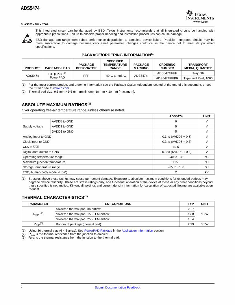
ABSOLUTE MAXIMUM RATINGS (1)
THERMAL CHARACTERISTICS (1)
ADS5474
SLAS525–JULY 2007
This integrated circuit can be damaged by ESD. Texas Instruments recommends that all integrated circuits be handled withappropriate precautions. Failure to observe proper handling and installation procedures can cause damage.
ESD damage can range from subtle performance degradation to complete device failure. Precision integrated circuits may bemore susceptible to damage because very small parametric changes could cause the device not to meet its publishedspecifications.
PACKAGE/ORDERING INFORMATION (1)
SPECIFIEDPACKAGE TEMPERATURE PACKAGE ORDERING TRANSPORT
PRODUCT PACKAGE-LEAD DESIGNATOR RANGE MARKING NUMBER MEDIA, QUANTITY
ADS5474IPFP Tray, 96HTQFP-80 (2)ADS5474 PFP –40°C to +85°C ADS5474IPowerPAD ADS5474IPFPR Tape and Reel, 1000
(1) For the most current product and ordering information see the Package Option Addendum located at the end of this document, or seethe TI web site at www.ti.com.
(2) Thermal pad size: 9.5 mm × 9.5 mm (minimum), 10 mm × 10 mm (maximum).
Over operating free-air temperature range, unless otherwise noted.
ADS5474 UNIT
AVDD5 to GND 6 V
Supply voltage AVDD3 to GND 5 V
DVDD3 to GND 5 V
Analog input to GND –0.3 to (AVDD5 + 0.3) V
Clock input to GND –0.3 to (AVDD5 + 0.3) V
CLK to CLK ±2.5 V
Digital data output to GND –0.3 to (DVDD3 + 0.3) V
Operating temperature range –40 to +85 °C
Maximum junction temperature +150 °C
Storage temperature range –65 to +150 °C
ESD, human-body model (HBM) 2 kV
(1) Stresses above these ratings may cause permanent damage. Exposure to absolute maximum conditions for extended periods maydegrade device reliability. These are stress ratings only, and functional operation of the device at these or any other conditions beyondthose specified is not implied. Kirkendall voidings and current density information for calculation of expected lifetime are available uponrequest.
PARAMETER TEST CONDITIONS TYP UNIT
Soldered thermal pad, no airflow 23.7
RθJA(2) Soldered thermal pad, 150-LFM airflow 17.8 °C/W
Soldered thermal pad, 250-LFM airflow 16.4
RθJP(3) Bottom of package (thermal pad) 2.99 °C/W
(1) Using 36 thermal vias (6 × 6 array). See PowerPAD Package in the Application Information section.(2) RθJA is the thermal resistance from the junction to ambient.(3) RθJP is the thermal resistance from the junction to the thermal pad.
2 Submit Documentation Feedback
www.ti.com
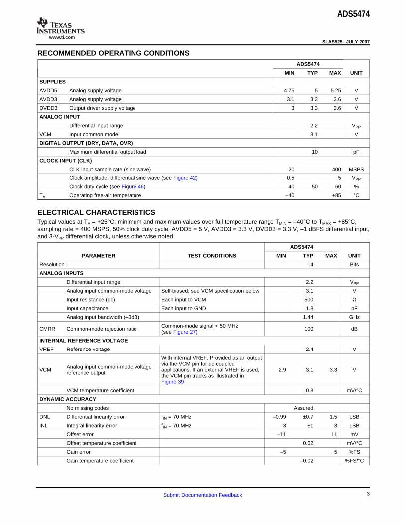
RECOMMENDED OPERATING CONDITIONS
ELECTRICAL CHARACTERISTICS
ADS5474
SLAS525–JULY 2007
ADS5474
MIN TYP MAX UNIT
SUPPLIES
AVDD5 Analog supply voltage 4.75 5 5.25 V
AVDD3 Analog supply voltage 3.1 3.3 3.6 V
DVDD3 Output driver supply voltage 3 3.3 3.6 V
ANALOG INPUT
Differential input range 2.2 VPP
VCM Input common mode 3.1 V
DIGITAL OUTPUT (DRY, DATA, OVR)
Maximum differential output load 10 pF
CLOCK INPUT (CLK)
CLK input sample rate (sine wave) 20 400 MSPS
Clock amplitude, differential sine wave (see Figure 42) 0.5 5 VPP
Clock duty cycle (see Figure 46) 40 50 60 %
TA Operating free-air temperature –40 +85 °C
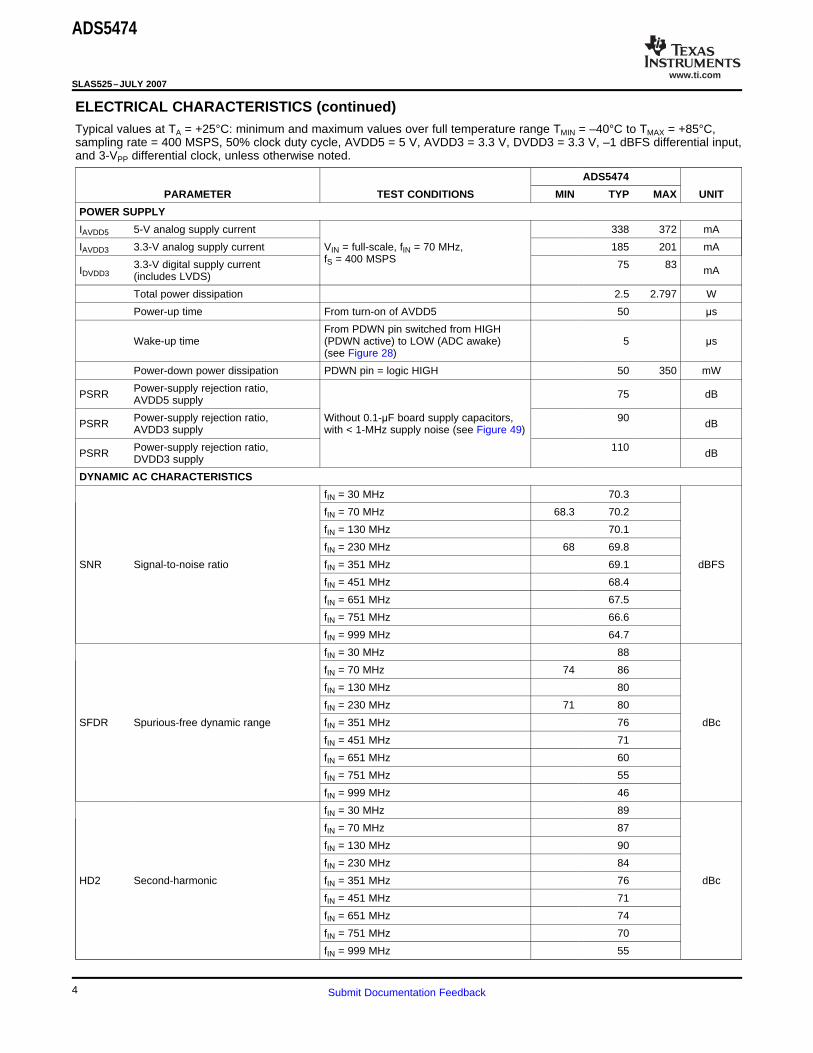
Typical values at TA = +25°C: minimum and maximum values over full temperature range TMIN = –40°C to TMAX = +85°C,sampling rate = 400 MSPS, 50% clock duty cycle, AVDD5 = 5 V, AVDD3 = 3.3 V, DVDD3 = 3.3 V, –1 dBFS differential input,and 3-VPP differential clock, unless otherwise noted.
ADS5474
PARAMETER TEST CONDITIONS MIN TYP MAX UNIT
Resolution 14 Bits
ANALOG INPUTS
Differential input range 2.2 VPP
Analog input common-mode voltage Self-biased; see VCM specification below 3.1 V
Input resistance (dc) Each input to VCM 500 Ω
Input capacitance Each input to GND 1.8 pF
Analog input bandwidth (–3dB) 1.44 GHz
Common-mode signal < 50 MHzCMRR Common-mode rejection ratio 100 dB(see Figure 27)
INTERNAL REFERENCE VOLTAGE
VREF Reference voltage 2.4 V
With internal VREF. Provided as an outputvia the VCM pin for dc-coupledAnalog input common-mode voltageVCM applications. If an external VREF is used, 2.9 3.1 3.3 Vreference output the VCM pin tracks as illustrated inFigure 39
VCM temperature coefficient –0.8 mV/°C
DYNAMIC ACCURACY
No missing codes Assured
DNL Differential linearity error fIN = 70 MHz –0.99 ±0.7 1.5 LSB
INL Integral linearity error fIN = 70 MHz –3 ±1 3 LSB
Offset error –11 11 mV
Offset temperature coefficient 0.02 mV/°C
Gain error –5 5 %FS
Gain temperature coefficient –0.02 %FS/°C
3Submit Documentation Feedback
www.ti.com
ADS5474
SLAS525–JULY 2007
ELECTRICAL CHARACTERISTICS (continued)Typical values at TA = +25°C: minimum and maximum values over full temperature range TMIN = –40°C to TMAX = +85°C,sampling rate = 400 MSPS, 50% clock duty cycle, AVDD5 = 5 V, AVDD3 = 3.3 V, DVDD3 = 3.3 V, –1 dBFS differential input,and 3-VPP differential clock, unless otherwise noted.
ADS5474
PARAMETER TEST CONDITIONS MIN TYP MAX UNIT
POWER SUPPLY
IAVDD5 5-V analog supply current 338 372 mA
IAVDD3 3.3-V analog supply current VIN = full-scale, fIN = 70 MHz, 185 201 mAfS = 400 MSPS3.3-V digital supply current 75 83IDVDD3 mA(includes LVDS)
Total power dissipation 2.5 2.797 W
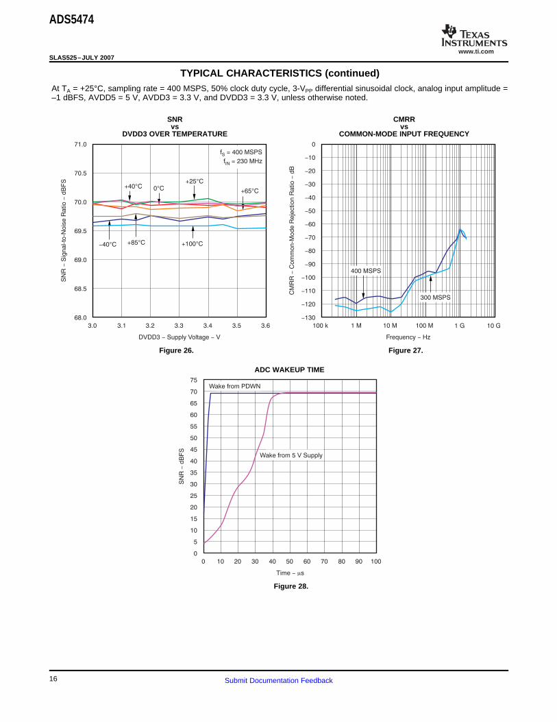
Power-up time From turn-on of AVDD5 50 μs
From PDWN pin switched from HIGHWake-up time (PDWN active) to LOW (ADC awake) 5 μs
(see Figure 28)
Power-down power dissipation PDWN pin = logic HIGH 50 350 mW
Power-supply rejection ratio,PSRR 75 dBAVDD5 supply
Power-supply rejection ratio, Without 0.1-μF board supply capacitors, 90PSRR dBAVDD3 supply with < 1-MHz supply noise (see Figure 49)
Power-supply rejection ratio, 110PSRR dBDVDD3 supply
DYNAMIC AC CHARACTERISTICS
fIN = 30 MHz 70.3
fIN = 70 MHz 68.3 70.2
fIN = 130 MHz 70.1
fIN = 230 MHz 68 69.8
SNR Signal-to-noise ratio fIN = 351 MHz 69.1 dBFS
fIN = 451 MHz 68.4
fIN = 651 MHz 67.5
fIN = 751 MHz 66.6
fIN = 999 MHz 64.7
fIN = 30 MHz 88
fIN = 70 MHz 74 86
fIN = 130 MHz 80
fIN = 230 MHz 71 80
SFDR Spurious-free dynamic range fIN = 351 MHz 76 dBc
fIN = 451 MHz 71
fIN = 651 MHz 60
fIN = 751 MHz 55
fIN = 999 MHz 46
fIN = 30 MHz 89
fIN = 70 MHz 87
fIN = 130 MHz 90
fIN = 230 MHz 84
HD2 Second-harmonic fIN = 351 MHz 76 dBc
fIN = 451 MHz 71
fIN = 651 MHz 74
fIN = 751 MHz 70
fIN = 999 MHz 55
4 Submit Documentation Feedback

www.ti.com
ADS5474
SLAS525–JULY 2007
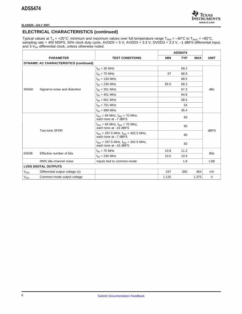
ELECTRICAL CHARACTERISTICS (continued)Typical values at TA = +25°C: minimum and maximum values over full temperature range TMIN = –40°C to TMAX = +85°C,sampling rate = 400 MSPS, 50% clock duty cycle, AVDD5 = 5 V, AVDD3 = 3.3 V, DVDD3 = 3.3 V, –1 dBFS differential input,and 3-VPP differential clock, unless otherwise noted.
ADS5474
PARAMETER TEST CONDITIONS MIN TYP MAX UNIT
DYNAMIC AC CHARACTERISTICS (continued)
fIN = 30 MHz 93
fIN = 70 MHz 86
fIN = 130 MHz 80
fIN = 230 MHz 80
HD3 Third-harmonic fIN = 351 MHz 85 dBc
fIN = 451 MHz 71
fIN = 651 MHz 60
fIN = 751 MHz 55
fIN = 999 MHz 46
fIN = 30 MHz 95
fIN = 70 MHz 93
fIN = 130 MHz 85
fIN = 230 MHz 85Worst harmonic/spur fIN = 351 MHz 87 dBc(other than HD2 and HD3)
fIN = 451 MHz 87
fIN = 651 MHz 90
fIN = 751 MHz 87
fIN = 999 MHz 80
fIN = 30 MHz 86
fIN = 70 MHz 83
fIN = 130 MHz 78
fIN = 230 MHz 77
THD Total harmonic distortion fIN = 351 MHz 75 dBc
fIN = 451 MHz 68
fIN = 651 MHz 60
fIN = 751 MHz 55
fIN = 999 MHz 45
5Submit Documentation Feedback
www.ti.com
ADS5474
SLAS525–JULY 2007
ELECTRICAL CHARACTERISTICS (continued)Typical values at TA = +25°C: minimum and maximum values over full temperature range TMIN = –40°C to TMAX = +85°C,sampling rate = 400 MSPS, 50% clock duty cycle, AVDD5 = 5 V, AVDD3 = 3.3 V, DVDD3 = 3.3 V, –1 dBFS differential input,and 3-VPP differential clock, unless otherwise noted.
ADS5474
PARAMETER TEST CONDITIONS MIN TYP MAX UNIT
DYNAMIC AC CHARACTERISTICS (continued)
fIN = 30 MHz 69.2
fIN = 70 MHz 67 68.9
fIN = 130 MHz 68.5
fIN = 230 MHz 65.5 68.2
SINAD Signal-to-noise and distortion fIN = 351 MHz 67.3 dBc
fIN = 451 MHz 64.8
fIN = 651 MHz 58.5
fIN = 751 MHz 54
fIN = 999 MHz 45.4
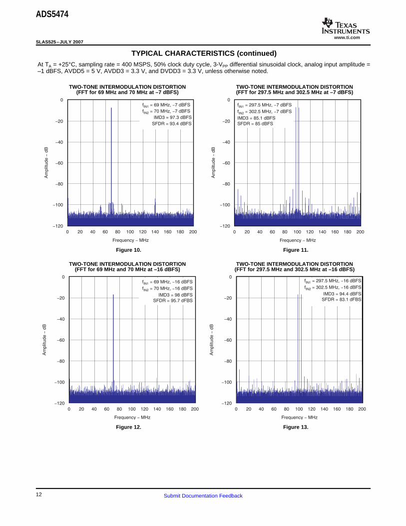
fIN1 = 69 MHz, fIN2 = 70 MHz, 93each tone at –7 dBFS
fIN1 = 69 MHz, fIN2 = 70 MHz, 95each tone at –16 dBFSTwo-tone SFDR dBFS
fIN1 = 297.5 MHz, fIN2 = 302.5 MHz, 85each tone at –7 dBFS
fIN1 = 297.5 MHz, fIN2 = 302.5 MHz, 83each tone at –16 dBFS
fIN = 70 MHz 10.8 11.2ENOB Effective number of bits Bits
fIN = 230 MHz 10.6 10.9
RMS idle-channel noise Inputs tied to common-mode 1.8 LSB
LVDS DIGITAL OUTPUTS
VOD Differential output voltage (±) 247 350 454 mV
VOC Common-mode output voltage 1.125 1.375 V
6 Submit Documentation Feedback
www.ti.com
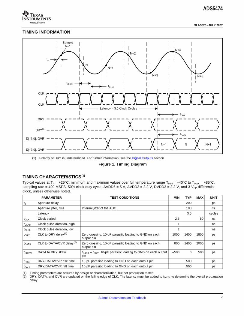
TIMING INFORMATION
N
CLK
D OVR[13:0],
N+1
N+5
tCLKL
tDRY
tDATA
tCLKH
ta
D[13:0], OVR
CLK
N+2
N+3
N+4
DRY
DRY(1)
N N+1N–1
SampleN–1
Latency = 3.5 Clock Cycles
TIMING CHARACTERISTICS (1)
ADS5474
SLAS525–JULY 2007
(1) Polarity of DRY is undetermined. For further information, see the Digital Outputs section.
Figure 1. Timing Diagram
Typical values at TA = +25°C: minimum and maximum values over full temperature range TMIN = –40°C to TMAX = +85°C,sampling rate = 400 MSPS, 50% clock duty cycle, AVDD5 = 5 V, AVDD3 = 3.3 V, DVDD3 = 3.3 V, and 3-VPP differentialclock, unless otherwise noted.
PARAMETER TEST CONDITIONS MIN TYP MAX UNIT
ta Aperture delay 200 ps
Aperture jitter, rms Internal jitter of the ADC 103 fs
Latency 3.5 cycles
tCLK Clock period 2.5 50 ns
tCLKH Clock pulse duration, high 1 ns
tCLKL Clock pulse duration, low 1 ns
tDRY CLK to DRY delay (2) Zero crossing, 10-pF parasitic loading to GND on each 1000 1400 1800 psoutput pin
tDATA CLK to DATA/OVR delay (2) Zero crossing, 10-pF parasitic loading to GND on each 800 1400 2000 psoutput pin
tSKEW DATA to DRY skew tDATA – tDRY, 10-pF parasitic loading to GND on each output –500 0 500 pspin
tRISE DRY/DATA/OVR rise time 10-pF parasitic loading to GND on each output pin 500 ps
tFALL DRY/DATA/OVR fall time 10-pF parasitic loading to GND on each output pin 500 ps
(1) Timing parameters are assured by design or characterization, but not production tested.(2) DRY, DATA, and OVR are updated on the falling edge of CLK. The latency must be added to tDATA to determine the overall propagation
delay.
7Submit Documentation Feedback

www.ti.com
PIN CONFIGURATION
22 23
D5A
VD
D5
D5G
ND
D4A
VD
D5
D4G
ND
D3A
VD
D5
D3G
ND
D2A
VD
D5
D2G
ND
GNDV
CM
DVDD3G
ND
D1A
VD
D5
D1G
ND
D0P
DW
N
D0G
ND
NCA
VD
D3
NCG
ND
NCA
VD
D3
NCG
ND
OVRA
VD
D3
OVRG
ND
60
59
58
57
56
55
54
53
52
51
50
49
48
47
46
45
44
43
42
41
24
1
2
3
4
5
6
7
8
9
10
11
12
13
14
15
16
17
18
19
20
DVDD3D
RY
GNDD
RY
AVDD5D
13
NCD
13
NCD
12
VREFD
12
GNDD
11
AVDD5D
11
GNDD
10
CLKD
10
CLKD
9
GNDD
9
AVDD5D
8
AVDD5D
8
GNDD
VD
D3
AING
ND
AIND
7
GNDD
7
AVDD5D
6
GNDD
6
25 26 27 28
79 78 77 76 7580 74 72 71 7073
29 30 31 32 33
69 68
21
67 66 65 64
34 35 36 37 38 39 40
63 62 61
ADS5474
ADS5474
SLAS525–JULY 2007
PFP PACKAGE(TOP VIEW)
8 Submit Documentation Feedback

www.ti.com
ADS5474
SLAS525–JULY 2007
PIN CONFIGURATION (continued)Table 1. TERMINAL FUNCTIONS
TERMINAL
NAME NO. DESCRIPTION
AIN 16 Differential input signal (positive)
AIN 17 Differential input signal (negative)
3, 8, 13, 14, 19, 21,AVDD5 Analog power supply (5 V)23, 25, 27, 31
Analog power supply (3.3 V) (Suggestion for ≤ 250 MSPS: leave option to connect to 5 V forAVDD3 35, 37, 39 ADS5440/ADS5444 13-bit compatibility)
DVDD3 1, 51, 66 Digital and output driver power supply (3.3 V)
2, 7, 9, 12, 15, 18,20, 22, 24, 26, 28,GND Ground30, 32, 34, 36, 38,
40, 52, 65
CLK 10 Differential input clock (positive). Conversion is initiated on rising edge.
CLK 11 Differential input clock (negative)
D0, D0 48, 47 LVDS digital output pair, least significant bit (LSB)
D1–D12, 49, 50, 53–64, LVDS digital output pairsD1–D10 67–76
D13, D13 78, 77 LVDS digital output pair, most significant bit (MSB)
DRY, DRY 80, 79 Data ready LVDS output pair
No connect (pins 4 and 5 should be left floating; pins 43 to 46 are possible future bit additions for thisNC 4, 5, 43–46 pinout and therefore can be connected to a digital bus or left floating)
Overrange indicator LVDS output. A logic high signals an analog input in excess of the full-scaleOVR, OVR 42, 41 range.
Common-mode voltage output (3.1 V nominal). Commonly used in DC-coupled applications to setVCM 29 the input signal to the correct common-mode voltage.
(This pin is not used on the ADS5440, ADS5444, and ADS5463)
Power-down (active high). Device is in sleep mode when PDWN pin is logic HIGH. ADC converter isPDWN 33 awake when PDWN is logic LOW (grounded).
(This pin is not used on the ADS5440, ADS5444, and ADS5463)
VREF 6 Reference voltage input/output (2.4 V nominal)
9Submit Documentation Feedback

www.ti.com
TYPICAL CHARACTERISTICS
Frequency MHz-
0
-20
-40
-60
-80
-100
-120
0 20 40 60 80 100 120 140 160 180 200
Am
plitu
de
dB
-
SFDR = 88.4 dBc
SNR = 70.3 dBFS
SINAD = 70.2 dBFS
THD = 86 dBc
Frequency MHz-
0
-20
-40
-60
-80
-100
-120
0 20 40 60 80 100 120 140 160 180 200
Am
plitu
de
dB
-
SFDR = 86.6 dBc
SNR = 70.1 dBFS
SINAD = 69.9 dBFS
THD = 82.9 dBc
Frequency MHz-
0
-20
-40
-60
-80
-100
-120
0 20 40 60 80 100 120 140 160 180 200
Am
plitu
de
dB
-
SFDR = 78.5 dBc
SNR = 70.1 dBFS
SINAD = 69.5 dBFS
THD = 77.4 dBc
Frequency MHz-
0
-20
-40
-60
-80
-100
-120
0 20 40 60 80 100 120 140 160 180 200
Am
plitu
de
dB
-
SFDR = 79.7 dBc
SNR = 69.8 dBFS
SINAD = 69.2 dBFS
THD = 76.9 dBc
ADS5474
SLAS525–JULY 2007
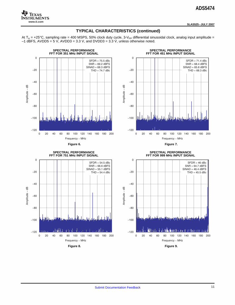
At TA = +25°C, sampling rate = 400 MSPS, 50% clock duty cycle, 3-VPP differential sinusoidal clock, analog input amplitude =–1 dBFS, AVDD5 = 5 V, AVDD3 = 3.3 V, and DVDD3 = 3.3 V, unless otherwise noted.
SPECTRAL PERFORMANCE SPECTRAL PERFORMANCEFFT FOR 30 MHz INPUT SIGNAL FFT FOR 70 MHz INPUT SIGNAL
Figure 2. Figure 3.
SPECTRAL PERFORMANCE SPECTRAL PERFORMANCEFFT FOR 130 MHz INPUT SIGNAL FFT FOR 230 MHz INPUT SIGNAL
Figure 4. Figure 5.
10 Submit Documentation Feedback
www.ti.com
Frequency MHz-
0
-20
-40
-60
-80
-100
-120
0 20 40 60 80 100 120 140 160 180 200
Am
plitu
de
dB
-
SFDR = 75.5 dBc
SNR = 69.2 dBFS
SINAD = 68.3 dBFS
THD = 74.7 dBc
Frequency MHz-
0
-20
-40
-60
-80
-100
-120
0 20 40 60 80 100 120 140 160 180 200
Am
plitu
de
dB
-
SFDR = 71.4 dBc
SNR = 68.4 dBFS
SINAD = 65.8 dBFS
THD = 68.3 dBc
Frequency MHz-
0
-20
-40
-60
-80
-100
-120
0 20 40 60 80 100 120 140 160 180 200
Am
plitu
de
dB
-
SFDR = 54.5 dBc
SNR = 66.6 dBFS
SINAD = 55.1 dBFS
THD = 54.4 dBc
Frequency MHz-
0
-20
-40
-60
-80
-100
-120
0 20 40 60 80 100 120 140 160 180 200
Am
plitu
de
dB
-
SFDR = 46 dBc
SNR = 64.7 dBFS
SINAD = 46.4 dBFS
THD = 45.5 dBc
ADS5474
SLAS525–JULY 2007
TYPICAL CHARACTERISTICS (continued)At TA = +25°C, sampling rate = 400 MSPS, 50% clock duty cycle, 3-VPP differential sinusoidal clock, analog input amplitude =–1 dBFS, AVDD5 = 5 V, AVDD3 = 3.3 V, and DVDD3 = 3.3 V, unless otherwise noted.
SPECTRAL PERFORMANCE SPECTRAL PERFORMANCEFFT FOR 351 MHz INPUT SIGNAL FFT FOR 451 MHz INPUT SIGNAL
Figure 6. Figure 7.
SPECTRAL PERFORMANCE SPECTRAL PERFORMANCEFFT FOR 751 MHz INPUT SIGNAL FFT FOR 999 MHz INPUT SIGNAL
Figure 8. Figure 9.
11Submit Documentation Feedback
www.ti.com
Frequency MHz-
0
-20
-40
-60
-80
-100
-120
0 20 40 60 80 100 120 140 160 180 200
Am
plitu
de
dB
-
f = 69 MHz, 7 dBFSIN1
-
f = 70 MHz, 7 dBFSIN2
-
IMD3 = 97.3 dBFS
SFDR = 93.4 dBFS
Frequency MHz-
0
-20
-40
-60
-80
-100
-120
0 20 40 60 80 100 120 140 160 180 200
Am
plitu
de
dB
-
f = 297.5 MHz, 7 dBFS
f = 302.5 MHz, 7 dBFS
IMD3 = 85.1 dBFS
SFDR = 85 dBFS
IN1
IN2
-
-
Frequency MHz-
0
-20
-40
-60
-80
-100
-120
0 20 40 60 200
Am
plitu
de
dB
-
80 100 120
f = 69 MHz, 16 dBFS
f = 70 MHz, 16 dBFS
IMD3 = 98 dBFS
SFDR = 95.7 dFBS
IN1
IN2
-
-
140 160 180
Frequency MHz-
0
-20
-40
-60
-80
-100
-120
0 20 40 60 200
Am
plitu
de
dB
-
80 100 120
f = 297.5 MHz, 16 dBFS
f = 302.5 MHz, 16 dBFS
IMD3 = 94.4 dBFS
SFDR = 83.1 dFBS
IN1
IN2
-
-
140 160 180
ADS5474
SLAS525–JULY 2007
TYPICAL CHARACTERISTICS (continued)At TA = +25°C, sampling rate = 400 MSPS, 50% clock duty cycle, 3-VPP differential sinusoidal clock, analog input amplitude =–1 dBFS, AVDD5 = 5 V, AVDD3 = 3.3 V, and DVDD3 = 3.3 V, unless otherwise noted.
TWO-TONE INTERMODULATION DISTORTION TWO-TONE INTERMODULATION DISTORTION(FFT for 69 MHz and 70 MHz at –7 dBFS) (FFT for 297.5 MHz and 302.5 MHz at –7 dBFS)
Figure 10. Figure 11.
TWO-TONE INTERMODULATION DISTORTION TWO-TONE INTERMODULATION DISTORTION(FFT for 69 MHz and 70 MHz at –16 dBFS) (FFT for 297.5 MHz and 302.5 MHz at –16 dBFS)
Figure 12. Figure 13.
12 Submit Documentation Feedback
www.ti.com
Frequency Hz-
3
0
-3
-6
-9
-12
-15
-18
-21
10 M 100 M 1 G 5 G
Norm
alized G
ain
dB
-
f = 400 MSPS
A = 0.38 V
S
IN PP±
Code
0.5
0.4
0.3
0.2
0.1
0
-0.1
-0.2
-0.3
-0.4
-0.5
0 2048 4096 6144 8192 10240 12288 14336 16384
DN
LLS
B-
f = 400 MSPSS
f = 70 MHzIN
Code
2.0
1.5
1.0
0.5
0
-0.5
-1.0
-1.5
-2.0
0 2048 4096 6144 8192 10240 12288 14336 16384
INL
LS
B-
f = 400 MSPSS
f = 70 MHzIN
Output Code
25
20
15
10
5
0
8227
Perc
enta
ge
%-
f = 400 MSPS
f = VCM
S
IN
8225
8223
8221
8219
8217
8215
8213
8211
8209
8207
8205
8226
8224
8222
8220
8218
8216
8214
8212
8210
8208
8206
ADS5474
SLAS525–JULY 2007
TYPICAL CHARACTERISTICS (continued)At TA = +25°C, sampling rate = 400 MSPS, 50% clock duty cycle, 3-VPP differential sinusoidal clock, analog input amplitude =–1 dBFS, AVDD5 = 5 V, AVDD3 = 3.3 V, and DVDD3 = 3.3 V, unless otherwise noted.
NORMALIZED GAIN RESPONSEvs
INPUT FREQUENCY DIFFERENTIAL NONLINEARITY
Figure 14. Figure 15.
INTEGRAL NONLINEARITY NOISE HISTOGRAM WITH INPUTS SHORTED
Figure 16. Figure 17.
13Submit Documentation Feedback

www.ti.com
Input Amplitude dBFS-
120
100
80
60
40
20
0
-20
-40
-100 -90 -80 -70 -60 -50 -40 -30 -20 -10 0
AC
Perf
orm
ance
dB
-
f = 400 MSPSS
f = 70 MHzIN
SFDR (dBc)
SFDR (dBFS)
SNR (dBc)
SNR (dBFS)
Input Amplitude dBFS-
120
100
80
60
40
20
0
-20
-40
-100 -90 -80 -70 -60 -50 -40 -30 -20 -10 0
AC
Perf
orm
ance
dB
-
f = 400 MSPSS
f = 230 MHzIN
SFDR (dBc)
SFDR (dBFS)
SNR (dBc)
SNR (dBFS)
AVDD5 Supply Voltage V- -
90
88
86
84
82
80
78
76
70
4.7 4.8 4.9 5.0 5.3
SF
DR
Spurious-F
ree D
ynam
ic R
ange
dB
c-
-
74
72
5.1 5.2
f = 400 MSPS
f = 230 MHz
S
IN
-40 C°
+25 C°+40 C° +65 C°
+100 C°
+85 C°0 C°
A dBFSIN
-
100
90
80
70
60
50
40
30
0
-100 -90 -80 -70 0
Perf
orm
ance
dB
-
20
10
-60 -50 -40 -30 -20 -10
2f f (dBc)-1 2
2f f (dBc)2 1
-
Worst Spur (dBc)
ADS5474
SLAS525–JULY 2007
TYPICAL CHARACTERISTICS (continued)At TA = +25°C, sampling rate = 400 MSPS, 50% clock duty cycle, 3-VPP differential sinusoidal clock, analog input amplitude =–1 dBFS, AVDD5 = 5 V, AVDD3 = 3.3 V, and DVDD3 = 3.3 V, unless otherwise noted.
AC PERFORMANCE AC PERFORMANCEvs vs
INPUT AMPLITUDE (70 MHz Input Signal) INPUT AMPLITUDE (230 MHz Input Signal)
Figure 18. Figure 19.
TWO-TONE PERFORMANCE SFDRvs vs
INPUT AMPLITUDE (f1 = 297.5 MHz and f2 = 302.5 MHz) AVDD5 OVER TEMPERATURE
Figure 20. Figure 21.
14 Submit Documentation Feedback

www.ti.com
AVDD5 Supply Voltage V- -
71.0
70.5
70.0
69.5
69.0
68.5
68.0
4.7 4.8 4.9 5.0 5.3
SN
RS
ignal-to
-Nois
e R
atio
dB
FS
--
5.1 5.2
f = 400 MSPS
f = 230 MHz
S
IN
- °40 C
+25 C°+40 C°
+65 C°
+100 C°
+85 C°0 C°
AVDD3 Supply Voltage V- -
90
88
86
84
82
80
78
76
70
3.0 3.1 3.2 3.3 3.6
SF
DR
Spurious-F
ree D
ynam
ic R
ange
dB
c-
-
74
72
3.4 3.5
f = 400 MSPS
f = 230 MHz
S
IN
- °40 C
+25 C° +40 C°+65 C°
+100 C°
+85 C°
0 C°
AVDD3 Supply Voltage V- -
71.0
70.5
70.0
69.5
69.0
68.5
68.0
3.0 3.1 3.2 3.3 3.6
SN
RS
ignal-to
-Nois
e R
atio
dB
FS
--
3.4 3.5
f = 400 MSPS
f = 230 MHz
S
IN
-40 C°
+25 C°+40 C°
+65 C°
+100 C°
+85 C°0 C°
DVDD3 Supply Voltage V- -
90
88
86
84
82
80
78
76
70
3.0 3.1 3.2 3.3 3.6
SF
DR
Spurious-F
ree D
ynam
ic R
ange
dB
c-
-
74
72
3.4 3.5
f = 400 MSPS
f = 230 MHz
S
IN
- °40 C +100 C°0 C°
+40 C°+65 C°
+85 C°
+25 C°
ADS5474
SLAS525–JULY 2007
TYPICAL CHARACTERISTICS (continued)At TA = +25°C, sampling rate = 400 MSPS, 50% clock duty cycle, 3-VPP differential sinusoidal clock, analog input amplitude =–1 dBFS, AVDD5 = 5 V, AVDD3 = 3.3 V, and DVDD3 = 3.3 V, unless otherwise noted.
SNR SFDRvs vs
AVDD5 OVER TEMPERATURE AVDD3 OVER TEMPERATURE
Figure 22. Figure 23.
SNR SFDRvs vs
AVDD3 OVER TEMPERATURE DVDD3 OVER TEMPERATURE
Figure 24. Figure 25.
15Submit Documentation Feedback
www.ti.com
DVDD3 Supply Voltage V- -
71.0
70.5
70.0
69.5
69.0
68.5
68.0
3.0 3.1 3.2 3.3 3.6
SN
RS
ignal-to
-Nois
e R
atio
dB
FS
--
3.4 3.5
f = 400 MSPS
f = 230 MHz
S
IN
- °40 C +100 C°
0 C°+40 C°+65 C°
+85 C°
+25 C°
Frequency Hz-
0
-10
-20
-30
-40
-50
-60
-70
-130
100 k 1 M 10 M 100 M 1 G 10 G
CM
RR
Com
mon-M
ode R
eje
ction R
atio
dB
--
-80
-90
-100
-110
-120
400 MSPS
300 MSPS
Time sm-
75
70
65
60
55
50
45
40
35
30
25
20
15
10
5
0
0 10 20 30 40 50 60 70 80 90 100
SN
RdB
FS
-
Wake from 5 V Supply
Wake from PDWN
ADS5474
SLAS525–JULY 2007
TYPICAL CHARACTERISTICS (continued)At TA = +25°C, sampling rate = 400 MSPS, 50% clock duty cycle, 3-VPP differential sinusoidal clock, analog input amplitude =–1 dBFS, AVDD5 = 5 V, AVDD3 = 3.3 V, and DVDD3 = 3.3 V, unless otherwise noted.
SNR CMRRvs vs
DVDD3 OVER TEMPERATURE COMMON-MODE INPUT FREQUENCY
Figure 26. Figure 27.
ADC WAKEUP TIME
Figure 28.
16 Submit Documentation Feedback

www.ti.com
70
70
70
7069
69
69
69
68
68
68
68
66
67
67
SNR dBFS-
54 56 58 60 62 64 68 70
10 100 200 300
66
400 500 600
f Input Frequency MHzIN
- -
fS
am
pling F
requency
MH
zS
--
400
350
300
250
200
150
100
40
SFDR dBc-
50 55 60 65 75 80 85 90
10 100 200
70
300 400 500 600
85
85
80
80
80
80 77
77
77
77
7773
73
73
70
70
70
65
65
6560
80
85
85
8585
f Input Frequency MHzIN
- -
fS
am
pling F
requency
MH
zS
--
400
350
300
250
200
150
100
40
ADS5474
SLAS525–JULY 2007
TYPICAL CHARACTERISTICS (continued)At TA = +25°C, sampling rate = 400 MSPS, 50% clock duty cycle, 3-VPP differential sinusoidal clock, analog input amplitude =–1 dBFS, AVDD5 = 5 V, AVDD3 = 3.3 V, and DVDD3 = 3.3 V, unless otherwise noted.
SNR vs INPUT FREQUENCY AND SAMPLING FREQUENCY
Figure 29.
SFDR vs INPUT FREQUENCY AND SAMPLING FREQUENCY
Figure 30.
17Submit Documentation Feedback

www.ti.com
APPLICATIONS INFORMATION
Theory of Operation
Input Configuration
ADS5474
AVDD5
AIN
AIN
GND
AVDD5
GND
GND
500 W
500 W
VCM
Buffer
Buffer
1.6 pF
1.6 pF
ADS5474
SLAS525–JULY 2007
The ADS5474 is a 14-bit, 400-MSPS, monolithic pipeline ADC. Its bipolar analog core operates from 5-V and3.3-V supplies, while the output uses a 3.3-V supply to provide LVDS-compatible outputs. The conversionprocess is initiated by the rising edge of the external input clock. At that instant, the differential input signal iscaptured by the input track-and-hold (T&H), and the input sample is converted sequentially by a series of lowerresolution stages, with the outputs combined in a digital correction logic block. Both the rising and the fallingclock edges are used to propagate the sample through the pipeline every half clock cycle. This process resultsin a data latency of 3.5 clock cycles, after which the output data are available as a 14-bit parallel word, coded inoffset binary format.
The analog input for the ADS5474 consists of an analog pseudo-differential buffer followed by a bipolartransistor T&H. The analog buffer isolates the source driving the input of the ADC from any internal switchingand presents a high impedance that is easy to drive at high input frequencies, compared to an ADC without abuffered input. The input common-mode is set internally through a 500-Ω resistor connected from 3.1 V to eachof the inputs. This configuration results in a differential input impedance of 1 kΩ.
Figure 31. Analog Input Circuit
For a full-scale differential input, each of the differential lines of the input signal (pins 16 and 17) swingssymmetrically between (3.1 V + 0.55 V) and (3.1 V – 0.55 V). This range means that each input has a maximumsignal swing of 1.1 VPP for a total differential input signal swing of 2.2 VPP. Operation below 2.2 VPP is allowable,with the characteristics of performance versus input amplitude demonstrated in Figure 18 and Figure 19. Forinstance, for performance at 1.1 VPP rather than 2.2 VPP, refer to the SNR and SFDR at –6 dBFS (0 dBFS =2.2 VPP). The maximum swing is determined by the internal reference voltage generator, eliminating the need forany external circuitry for this purpose.
18 Submit Documentation Feedback
www.ti.com
R
50
0
W
Z
50
0
W
ADS5474
AIN
AIN
R
200 WAC Signal
Source
Mini-Circuits
JTX-4-10T
ADS5474
THS9001 AIN
AIN
VIN
VIN THS9001
1000 pF 1000 pF
39 pF
50 W
50 W0.1 Fm
1000 pF 1000 pF
18 Hm
ADS5474
SLAS525–JULY 2007
Applications Information (continued)
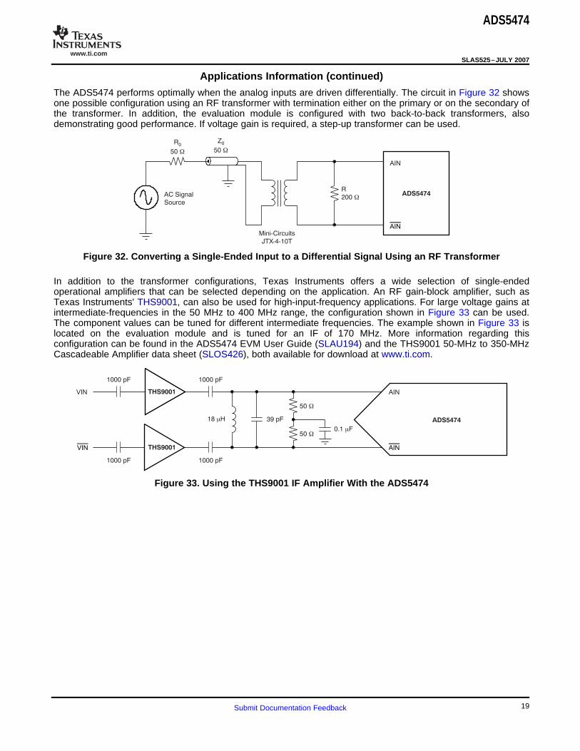
The ADS5474 performs optimally when the analog inputs are driven differentially. The circuit in Figure 32 showsone possible configuration using an RF transformer with termination either on the primary or on the secondary ofthe transformer. In addition, the evaluation module is configured with two back-to-back transformers, alsodemonstrating good performance. If voltage gain is required, a step-up transformer can be used.
Figure 32. Converting a Single-Ended Input to a Differential Signal Using an RF Transformer
In addition to the transformer configurations, Texas Instruments offers a wide selection of single-endedoperational amplifiers that can be selected depending on the application. An RF gain-block amplifier, such asTexas Instruments' THS9001, can also be used for high-input-frequency applications. For large voltage gains atintermediate-frequencies in the 50 MHz to 400 MHz range, the configuration shown in Figure 33 can be used.The component values can be tuned for different intermediate frequencies. The example shown in Figure 33 islocated on the evaluation module and is tuned for an IF of 170 MHz. More information regarding thisconfiguration can be found in the ADS5474 EVM User Guide (SLAU194) and the THS9001 50-MHz to 350-MHzCascadeable Amplifier data sheet (SLOS426), both available for download at www.ti.com.
Figure 33. Using the THS9001 IF Amplifier With the ADS5474
19Submit Documentation Feedback
www.ti.com
18 pF
AIN
AIN VCM
ADS5474
+5V
THS4509
CM
348 W
348 W
100 W
100 W
78.9 W
78.9 W49.9 W
VIN
From
50
Source
W
49.9 W
49.9 W
49.9 W
0.1 Fm 0.1 Fm
0.22 Fm
0.22 Fm0.22 Fm
ADS5474
SLAS525–JULY 2007
Applications Information (continued)
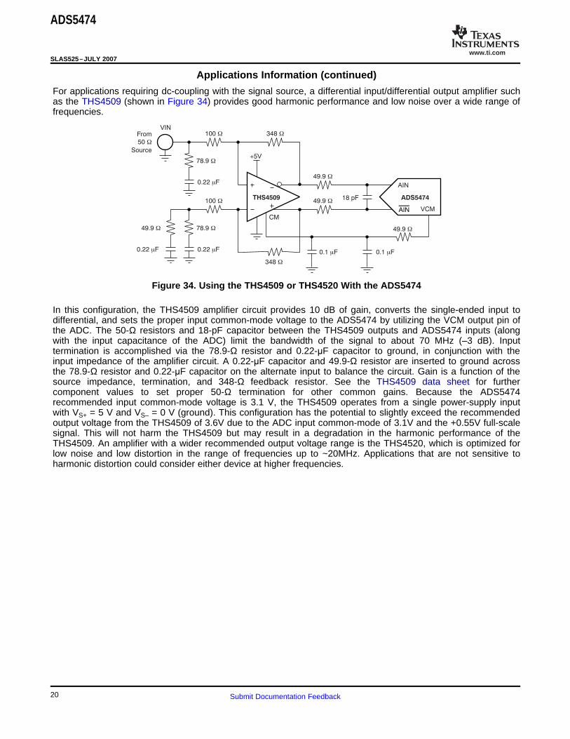
For applications requiring dc-coupling with the signal source, a differential input/differential output amplifier suchas the THS4509 (shown in Figure 34) provides good harmonic performance and low noise over a wide range offrequencies.
Figure 34. Using the THS4509 or THS4520 With the ADS5474
In this configuration, the THS4509 amplifier circuit provides 10 dB of gain, converts the single-ended input todifferential, and sets the proper input common-mode voltage to the ADS5474 by utilizing the VCM output pin ofthe ADC. The 50-Ω resistors and 18-pF capacitor between the THS4509 outputs and ADS5474 inputs (alongwith the input capacitance of the ADC) limit the bandwidth of the signal to about 70 MHz (–3 dB). Inputtermination is accomplished via the 78.9-Ω resistor and 0.22-μF capacitor to ground, in conjunction with theinput impedance of the amplifier circuit. A 0.22-μF capacitor and 49.9-Ω resistor are inserted to ground acrossthe 78.9-Ω resistor and 0.22-μF capacitor on the alternate input to balance the circuit. Gain is a function of thesource impedance, termination, and 348-Ω feedback resistor. See the THS4509 data sheet for furthercomponent values to set proper 50-Ω termination for other common gains. Because the ADS5474recommended input common-mode voltage is 3.1 V, the THS4509 operates from a single power-supply inputwith VS+ = 5 V and VS– = 0 V (ground). This configuration has the potential to slightly exceed the recommendedoutput voltage from the THS4509 of 3.6V due to the ADC input common-mode of 3.1V and the +0.55V full-scalesignal. This will not harm the THS4509 but may result in a degradation in the harmonic performance of theTHS4509. An amplifier with a wider recommended output voltage range is the THS4520, which is optimized forlow noise and low distortion in the range of frequencies up to ~20MHz. Applications that are not sensitive toharmonic distortion could consider either device at higher frequencies.
20 Submit Documentation Feedback

www.ti.com
External Voltage Reference
External VREF Applied V-
1.0
0.5
0
-0.5
-1.0
-1.5
-3.0
2.2 2.3 2.4 2.5 3.1
Norm
alized G
ain
Adju
stm
ent
dB
-
2.6 2.7 2.8
f = 400 MSPS
f = 70 MHz
A = < 1 dBFS
S
IN
IN-
2.9 3.0
Best Fit:
y = 3.14x + 7.5063-
-2.0
-2.5
External VREF Applied V-
90
80
70
60
50
40
2.05 2.15 2.25 2.35 2.45 3.15
SF
DR
Spurious-F
ree D
ynam
ic R
ange
dB
c-
-
f = 400 MSPS
f = 70 MHz
S
IN
2.55 2.65 2.75 2.85 2.95 3.05
A = 6 dBFS-IN
A = 4 dBFS-IN
A = 3 dBFS-IN
A = 5 dBFS-IN
A = 2 dBFS-IN
A = 1 dBFS-IN
ADS5474
SLAS525–JULY 2007
Applications Information (continued)
For systems that require the analog signal gain to be adjusted or calibrated, this can be performed by using anexternal reference. The dependency on the signal amplitude to the value of the external reference voltage ischaracterizaed typically by Figure 35 (VREF = 2.4 V is normalized to 0 dB as this is the internal referencevoltage). As can be seen in the linear fit, this equates to approximately –0.3 dB of signal adjustment per 100 mVof reference adjustment. The range of allowable variation depends on the analog input amplitude that is appliedto the inputs and the desired spectral performance, as can be seen in the performance versus externalreference graphs in Figure 36 and Figure 37. As the applied analog signal amplitude is reduced, more variationin the reference voltage is allowed in the positive direction (which equates to a reduction in signal amplitude),whereas an adjustment in reference voltage below the nominal 2.4 V (which equates to an increase in signalamplitude) is not recommended below approximately 2.35 V. The power consumption versus reference voltageand operating temperature should also be considered, especially at high ambient temperatures, because thelifetime of the device is affected by internal junction temperature, see Figure 50.
For dc-coupled applications that use the VCM pin of the ADS5474 as the common mode of the signal in theanalog signal gain path prior to the ADC inputs, the information in Figure 39 is useful to consider versus theallowable common-mode range of the device that is receiving the VCM voltage, such as an operational amplifier.Because it is pin-compatible, it is important to note that the ADS5463 does not have a VCM pin and primarilyuses the VREF pin to provide the common-mode voltage in dc-coupled applications. The ADS5463 (VCM = 2.4V) and ADS5474 (VCM = 3.1V) do not have the same common-mode voltage. To create a board layout that mayaccomodate both devices in dc-coupled applications, route VCM and VREF both to a common point that can beselected via a switch, jumper, or a 0 Ω resistor.
Figure 35. Signal Gain Adjustment versus External Figure 36. SFDR versus External VREF and AINReference (VREF)
21Submit Documentation Feedback

www.ti.com
External VREF Applied V-
75
70
65
60
55
50
45
40
2.05 2.15 2.25 2.35 2.45 3.15
SN
RS
ignal-to
-Nois
e R
atio
V-
-
f = 400 MSPS
f = 70 MHz
S
IN
2.55 2.65 2.75 2.85 2.95 3.05
A = 4 dBFS-IN
A = 3 dBFS-IN
A = 2 dBFS-IN
A = 1 dBFS-IN
A = 5 dBFS-IN
A = 6 dBFS-IN
External VREF Applied V-
3.4
3.2
3.0
2.8
2.6
2.4
2.2
2.0
2.05 2.15 2.25 2.35 2.45 3.15
Pow
er
W-
f = 400 MSPS
f = 70 MHz
S
IN
2.55 2.65 2.75 2.85 2.95 3.05
External VREF Applied V-
3.8
3.7
3.6
3.5
3.4
3.3
3.2
3.1
2.8
2.05 2.15 2.25 2.35 2.45 3.15
VC
M P
in O
utp
ut V
oltage
V-
3.0
2.9
f = 400 MSPS
f = 70 MHz
S
IN
2.55 2.65 2.75 2.85 2.95 3.05
ADS5474
SLAS525–JULY 2007
Applications Information (continued)
Figure 37. SNR versus External VREF and AIN Figure 38. Total Power Consumption versus ExternalVREF
Figure 39. VCM Pin Output versus External VREF
22 Submit Documentation Feedback

www.ti.com
Clock Inputs
ADS5474
AVDD5
CLK
CLK
GND
AVDD5
GND
GND
1 kW
1 kW
~2.4 V
Parasitic
~200 fF
Parasitic
~200 fF
Clock
Buffer
CLK
ADS5474
CLK
Square Wave or
Sine Wave
0.01 Fm
0.01 Fm
Clock Amplitude V-PP
90
85
80
75
70
65
60
0 0.5 1.0 1.5 5.0
AC
Perf
orm
ance
dB
-
2.0 2.5 3.0
f = 400 MSPS
f = 230 MHz
S
IN
3.5 4.0 4.5
SFDR (dBc)
SNR (dBFS)
ADS5474
SLAS525–JULY 2007
Applications Information (continued)
The ADS5474 clock input can be driven with either a differential clock signal or a single-ended clock input, asshown in Figure 40. The characterization of the ADS5474 is typically performed with a 3-VPP differential clock,but the ADC performs well with a differential clock amplitude down to ~0.5 VPP, as shown in Figure 42. Theclock amplitude becomes more of a factor in performance as the analog input frequency increases. Inlow-input-frequency applications, where jitter may not be a big concern, the use of a single-ended clock (asshown in Figure 41) could save cost and board space without much performance tradeoff. When clocked withthis configuration, it is best to connect CLK to ground with a 0.01-μF capacitor, while CLK is ac-coupled with a0.01-μF capacitor to the clock source, as shown in Figure 41.
Figure 40. Clock Input Circuit
Figure 41. Single-Ended Clock Figure 42. AC Performance versus Clock Level
23Submit Documentation Feedback

www.ti.com
CLK
ADS5474
CLK
0.1 Fm
Clock
Source
Clock Common Mode V-
90
85
80
75
70
65
50
0 1 5
SF
DR
Spurious-F
ree D
ynam
ic R
ange
dB
c-
-
2 3 4
60
55f = 400 MSPS
V = 3 V
S
CLK PP
230 MHz
351 MHz
70 MHz 10 MHz
Clock Common Mode V-
75
70
65
50
0 1 5
SN
RS
ignal-to
-Nois
e R
atio
dB
FS
--
2 3 4
60
55
f = 400 MSPS
V = 3 V
S
CLK PP
230 MHz
351 MHz 70 MHz
10 MHz
ADS5474
SLAS525–JULY 2007
For jitter-sensitive applications, the use of a differential clock has some advantages at the system level. Thedifferential clock allows for common-mode noise rejection at the printed circuit board (PCB) level. With adifferential clock, the signal-to-noise ratio of the ADC is better for jitter-sensitive, high-frequency applicationsbecause the board level clock jitter is superior.
Larger clock amplitude levels are recommended for high analog input frequencies or slow clock frequencies. Inthe case of a sinusoidal clock, larger amplitudes result in higher clock slew rates and reduces the impact ofclock noise on jitter. At high analog input frequencies, the sampling process is sensitive to jitter. And at slowclock frequencies, a small amplitude sinusoidal clock has a lower slew rate and can create jitter-related SNRdegradation. Figure 43 demonstrates a recommended method for converting a single-ended clock source into adifferential clock; it is similar to the configuration found on the evaluation board and was used for much of thecharacterization. See also Clocking High Speed Data Converters (SLYT075) for more details.
Figure 43. Differential Clock
The common-mode voltage of the clock inputs is set internally to 2.4 V using internal 1-kΩ resistors. It isrecommended to use ac coupling, but if this scheme is not possible, the ADS5474 features good tolerance toclock common-mode variation (as shown in Figure 44 and Figure 45). Additionally, the internal ADC core usesboth edges of the clock for the conversion process. Ideally, a 50% duty-cycle clock signal should be provided.Performance degradation as a result of duty cycle can be seen in Figure 46.
Figure 44. SFDR versus Clock Common Mode Figure 45. SNR versus Clock Common Mode
24 Submit Documentation Feedback

www.ti.com
Clock Duty Cycle %-
90
85
70
65
60
55
50
20 30 40 50 80
SF
DR
Spurious-F
ree D
ynam
ic R
ange
dB
c-
-
60 70
80
75
f = 400 MSPS
Clock Input = 3 V
S
PP
f = 10 MHzIN
f = 70 MHzIN
f = 230 MHzIN
f = 300 MHzIN
SNR (dBc) = 20 LOG10 (2 f j )- p ´´ ´ ´IN TOTAL (1)
j = (j + j )TOTAL ADC CLOCK
2 1/22
(2)
ADS5474
SLAS525–JULY 2007
Figure 46. SFDR vs Clock Duty Cycle
The ADS5474 is capable of achieving 69.2 dBFS SNR at 350 MHz of analog input frequency. In order toachieve the SNR at 350 MHz the clock source rms jitter must be at least 144 fsec in order for the total rms jitterto be 177 fsec. A summary of maximum recommended rms clock jitter as a function of analog input frequency isprovided in Table 2. The equations used to create the table are also presented.
Table 2. Recommended RMS Clock Jitter
INPUT FREQUENCY MEASURED SNR TOTAL JITTER MAXIMUM CLOCK JITTER(MHz) (dBc) (fsec rms) (fsec rms)
30 69.3 1818 1816
70 69.1 798 791
130 69.1 429 417
230 68.8 251 229
350 68.2 177 144
450 67.4 151 110
750 65.6 111 42
1000 63.7 104 14
Equation 1 and Equation 2 are used to estimate the required clock source jitter.
where:jTOTAL = the rms summation of the clock and ADC aperture jitter;jADC = the ADC internal aperture jitter which is located in the data sheet;jCLOCK = the rms jitter of the clock at the clock input pins to the ADC; andfIN = the analog input frequency.
Notice that the SNR is a strong function of the analog input frequency, not the clock frequency. The slope of theclock source edges can have a mild impact on SNR as well and is not taken into account for these estimates.For this reason, maximizing clock source amplitudes at the ADC clock inputs is recommended, though notrequired (faster slope is desireable for jitter-related SNR). For more information on clocking high-speed ADCs,see Application Note SLWA034, Implementing a CDC7005 Low Jitter Clock Solution For High-Speed, High-IF
25Submit Documentation Feedback
www.ti.com
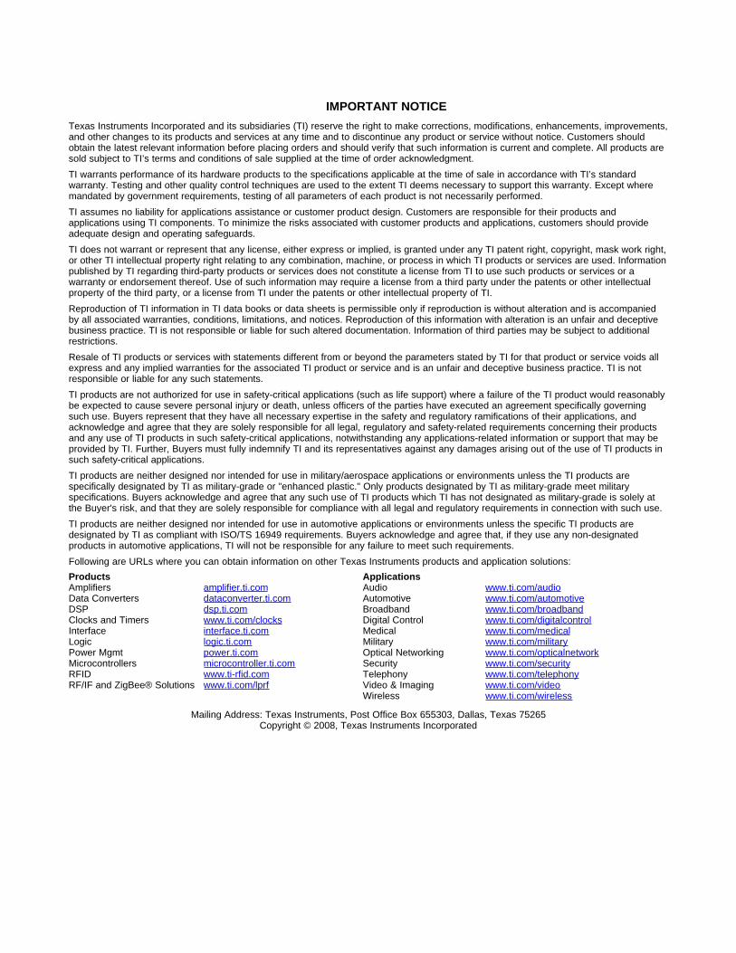
This is an example block diagram.
Low-Jitter Clock Distribution
ADC
ADS5474
VCXO
REF
CDC
(Clock Distribution Chip)
CDCM7005
800 MHz (to transmit DAC)
100 MHz (to DSP)
200 MHz (to FPGA)
To Other
Board Master
Reference Clock
(high or low jitter)
10 MHz400 MHz
Low-Jitter Oscillator
800 MHz
BPFLVCMOS
LVPECL
or
LVCMOS
XFMRAMP
CLKIN
CLKIN
¼
AMP and/or BPF are Optional
ADS5474
SLAS525–JULY 2007
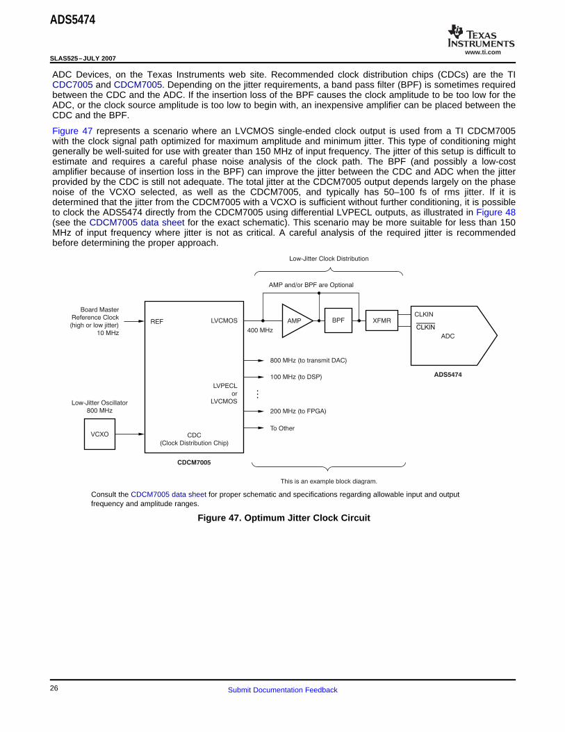
ADC Devices, on the Texas Instruments web site. Recommended clock distribution chips (CDCs) are the TICDC7005 and CDCM7005. Depending on the jitter requirements, a band pass filter (BPF) is sometimes requiredbetween the CDC and the ADC. If the insertion loss of the BPF causes the clock amplitude to be too low for theADC, or the clock source amplitude is too low to begin with, an inexpensive amplifier can be placed between theCDC and the BPF.
Figure 47 represents a scenario where an LVCMOS single-ended clock output is used from a TI CDCM7005with the clock signal path optimized for maximum amplitude and minimum jitter. This type of conditioning mightgenerally be well-suited for use with greater than 150 MHz of input frequency. The jitter of this setup is difficult toestimate and requires a careful phase noise analysis of the clock path. The BPF (and possibly a low-costamplifier because of insertion loss in the BPF) can improve the jitter between the CDC and ADC when the jitterprovided by the CDC is still not adequate. The total jitter at the CDCM7005 output depends largely on the phasenoise of the VCXO selected, as well as the CDCM7005, and typically has 50–100 fs of rms jitter. If it isdetermined that the jitter from the CDCM7005 with a VCXO is sufficient without further conditioning, it is possibleto clock the ADS5474 directly from the CDCM7005 using differential LVPECL outputs, as illustrated in Figure 48(see the CDCM7005 data sheet for the exact schematic). This scenario may be more suitable for less than 150MHz of input frequency where jitter is not as critical. A careful analysis of the required jitter is recommendedbefore determining the proper approach.
Consult the CDCM7005 data sheet for proper schematic and specifications regarding allowable input and outputfrequency and amplitude ranges.
Figure 47. Optimum Jitter Clock Circuit
26 Submit Documentation Feedback
www.ti.com
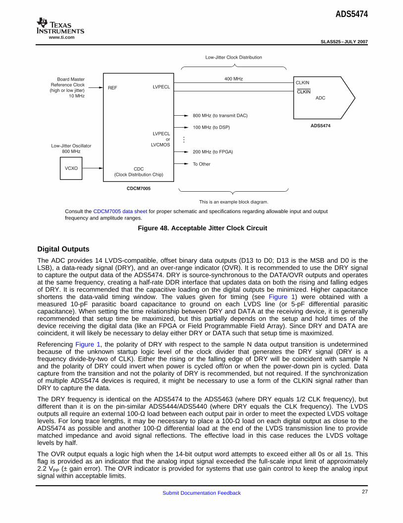
This is an example block diagram.
Low-Jitter Clock Distribution
ADC
ADS5474
VCXO
REF
CDC
(Clock Distribution Chip)
CDCM7005
800 MHz (to transmit DAC)
100 MHz (to DSP)
200 MHz (to FPGA)
To Other
Board Master
Reference Clock
(high or low jitter)
10 MHz
400 MHz
Low-Jitter Oscillator
800 MHz
LVPECL
LVPECL
or
LVCMOS
CLKIN
CLKIN
¼
Digital Outputs
ADS5474
SLAS525–JULY 2007
Consult the CDCM7005 data sheet for proper schematic and specifications regarding allowable input and outputfrequency and amplitude ranges.
Figure 48. Acceptable Jitter Clock Circuit
The ADC provides 14 LVDS-compatible, offset binary data outputs (D13 to D0; D13 is the MSB and D0 is theLSB), a data-ready signal (DRY), and an over-range indicator (OVR). It is recommended to use the DRY signalto capture the output data of the ADS5474. DRY is source-synchronous to the DATA/OVR outputs and operatesat the same frequency, creating a half-rate DDR interface that updates data on both the rising and falling edgesof DRY. It is recommended that the capacitive loading on the digital outputs be minimized. Higher capacitanceshortens the data-valid timing window. The values given for timing (see Figure 1) were obtained with ameasured 10-pF parasitic board capacitance to ground on each LVDS line (or 5-pF differential parasiticcapacitance). When setting the time relationship between DRY and DATA at the receiving device, it is generallyrecommended that setup time be maximized, but this partially depends on the setup and hold times of thedevice receiving the digital data (like an FPGA or Field Programmable Field Array). Since DRY and DATA arecoincident, it will likely be necessary to delay either DRY or DATA such that setup time is maximized.
Referencing Figure 1, the polarity of DRY with respect to the sample N data output transition is undeterminedbecause of the unknown startup logic level of the clock divider that generates the DRY signal (DRY is afrequency divide-by-two of CLK). Either the rising or the falling edge of DRY will be coincident with sample Nand the polarity of DRY could invert when power is cycled off/on or when the power-down pin is cycled. Datacapture from the transition and not the polarity of DRY is recommended, but not required. If the synchronizationof multiple ADS5474 devices is required, it might be necessary to use a form of the CLKIN signal rather thanDRY to capture the data.
The DRY frequency is identical on the ADS5474 to the ADS5463 (where DRY equals 1/2 CLK frequency), butdifferent than it is on the pin-similar ADS5444/ADS5440 (where DRY equals the CLK frequency). The LVDSoutputs all require an external 100-Ω load between each output pair in order to meet the expected LVDS voltagelevels. For long trace lengths, it may be necessary to place a 100-Ω load on each digital output as close to theADS5474 as possible and another 100-Ω differential load at the end of the LVDS transmission line to providematched impedance and avoid signal reflections. The effective load in this case reduces the LVDS voltagelevels by half.
The OVR output equals a logic high when the 14-bit output word attempts to exceed either all 0s or all 1s. Thisflag is provided as an indicator that the analog input signal exceeded the full-scale input limit of approximately2.2 VPP (± gain error). The OVR indicator is provided for systems that use gain control to keep the analog inputsignal within acceptable limits.
27Submit Documentation Feedback

www.ti.com
Power Supplies
Frequency Hz-
0
-10
-20
-30
-40
-50
-60
-70
-120
100 k 1 M 10 M 100 M 1 G
PS
RR
Pow
er-
Supply
Reje
ction R
atio
dB
--
-80
-90
-100
-110
f = 400 MSPSS
AVDD5
AVDD3
DVDD3
ADS5474
SLAS525–JULY 2007
The ADS5474 uses three power supplies. For the analog portion of the design, a 5-V and 3.3-V supply (AVDD5and AVDD3) are used, while the digital portion uses a 3.3-V supply (DVDD3). All the ground pins are marked asGND, although analog and digital grounds are not tied together inside the package. The use of low-noise powersupplies with adequate decoupling is recommended. Linear supplies are preferred to switched supplies;switched supplies tend to generate more noise components that can be coupled to the ADS5474. However, thePSRR value and plot shown in Figure 49 were obtained without bulk supply decoupling capacitors. When bulk(0.1 μF) decoupling capacitors are used, the board-level PSRR is much higher than the stated value for theADC. The user may be able to supply power to the device with a less-than-ideal supply and still achieve verygood performance. It is not possible to make a single recommendation for every type of supply and level ofdecoupling for all systems. If the noise characteristics of the available supplies are understood, a study of thePSRR data for the ADS5474 may provide the user with enough information to select noisy supplies if theperformance is still acceptable within the frequency range of interest. The power consumption of the ADS5474does not change substantially over clock rate or input frequency as a result of the architecture and process. Thetotal maximum ensured power supersedes the summation of the maximum individual supply currents.
Figure 49. PSRR versus Supply Injected Frequency
28 Submit Documentation Feedback
www.ti.com
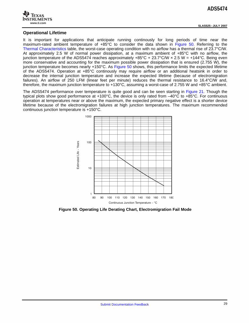
Operational Lifetime
Continuous Junction Temperature C°-
1000
100
10
1
80 90 100 110 120 130 140 150 160 170 180
Estim
ate
d L
ife
Years
-
ADS5474
SLAS525–JULY 2007
It is important for applications that anticipate running continously for long periods of time near themaximum-rated ambient temperature of +85°C to consider the data shown in Figure 50. Referring to theThermal Characteristics table, the worst-case operating condition with no airflow has a thermal rise of 23.7°C/W.At approximately 2.5 W of normal power dissipation, at a maximum ambient of +85°C with no airflow, thejunction temperature of the ADS5474 reaches approximately +85°C + 23.7°C/W × 2.5 W = +144°C. Being evenmore conservative and accounting for the maximum possible power dissipation that is ensured (2.755 W), thejunction temperature becomes nearly +150°C. As Figure 50 shows, this performance limits the expected lifetimeof the ADS5474. Operation at +85°C continously may require airflow or an additional heatsink in order todecrease the internal junction temperature and increase the expected lifetime (because of electromigrationfailures). An airflow of 250 LFM (linear feet per minute) reduces the thermal resistance to 16.4°C/W and,therefore, the maximum junction temperature to +130°C, assuming a worst-case of 2.755 W and +85°C ambient.
The ADS5474 performance over temperature is quite good and can be seen starting in Figure 21. Though thetypical plots show good performance at +100°C, the device is only rated from –40°C to +85°C. For continuousoperation at temperatures near or above the maximum, the expected primary negative effect is a shorter devicelifetime because of the electromigration failures at high junction temperatures. The maximum recommendedcontinuous junction temperature is +150°C.
Figure 50. Operating Life Derating Chart, Electromigration Fail Mode
29Submit Documentation Feedback

www.ti.com
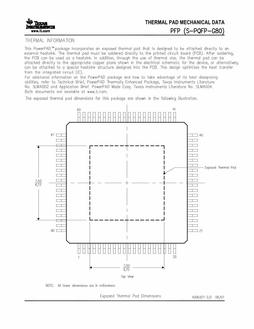
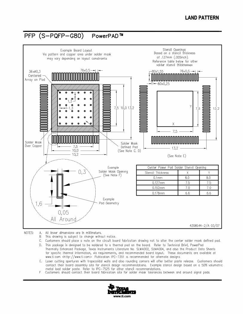
Layout Information
PowerPAD Package
Assembly Process
ADS5474
SLAS525–JULY 2007
The evaluation board represents a good model of how to lay out the printed circuit board (PCB) to obtain themaximum performance from the ADS5474. Follow general design rules, such as the use of multilayer boards, asingle ground plane for ADC ground connections, and local decoupling ceramic chip capacitors. The analoginput traces should be isolated from any external source of interference or noise, including the digital outputs aswell as the clock traces. The clock signal traces should also be isolated from other signals, especially inapplications such as high IF sampling where low jitter is required. Besides performance-oriented rules, caremust be taken when considering the heat dissipation of the device. The thermal heatsink included on the bottomof the package should be soldered to the board as described in the PowerPad Package section. See theADS5474 EVM User Guide (SLAU194) on the TI web site for the evaluation board schematic.
The PowerPAD package is a thermally-enhanced, standard-size IC package designed to eliminate the use ofbulky heatsinks and slugs traditionally used in thermal packages. This package can be easily mounted usingstandard PCB assembly techniques, and can be removed and replaced using standard repair procedures.
The PowerPAD package is designed so that the leadframe die pad (or thermal pad) is exposed on the bottom ofthe IC. This pad design provides an extremely low thermal resistance path between the die and the exterior ofthe package. The thermal pad on the bottom of the IC can then be soldered directly to the PCB, using the PCBas a heatsink.
1. Prepare the PCB top-side etch pattern including etch for the leads as well as the thermal pad asillustrated in the Mechanical Data section (at the end of this data sheet).
2. Place a 6-by-6 array of thermal vias in the thermal pad area. These holes should be 13 mils (0.013 in or0.3302 mm) in diameter. The small size prevents wicking of the solder through the holes.
3. It is recommended to place a small number of 25 mil (0.025 in or 0.635 mm) diameter holes under thepackage, but outside the thermal pad area, to provide an additional heat path.
4. Connect all holes (both those inside and outside the thermal pad area) to an internal copper plane (suchas a ground plane).
5. Do not use the typical web or spoke via-connection pattern when connecting the thermal vias to theground plane. The spoke pattern increases the thermal resistance to the ground plane.
6. The top-side solder mask should leave exposed the terminals of the package and the thermal pad area.7. Cover the entire bottom side of the PowerPAD vias to prevent solder wicking.8. Apply solder paste to the exposed thermal pad area and all of the package terminals.
For more detailed information regarding the PowerPAD package and its thermal properties, see either thePowerPAD Made Easy application brief (SLMA004) or the PowerPAD Thermally Enhanced Package applicationreport (SLMA002), both available for download at www.ti.com.
30 Submit Documentation Feedback
www.ti.com
DEFINITION OF SPECIFICATIONS
SNR 10log10PSPN (4)
SINAD 10log10PS
PN PD (5)
THD 10log10PSPD (6)
ADS5474
SLAS525–JULY 2007
The injected frequency level is translated into dBFS,the spur in the output FFT is measured in dBFS, and
Analog Bandwidth the difference is the PSRR in dB. The measurementThe analog input frequency at which the power of the calibrates out the benefit of the board supplyfundamental is reduced by 3 dB with respect to the decoupling capacitors.low-frequency value.
Signal-to-Noise Ratio (SNR)Aperture Delay SNR is the ratio of the power of the fundamental (PS)The delay in time between the rising edge of the to the noise floor power (PN), excluding the power atinput sampling clock and the actual time at which the dc and in the first five harmonics.sampling occurs.
Aperture Uncertainty (Jitter)The sample-to-sample variation in aperture delay.
SNR is either given in units of dBc (dB to carrier)Clock Pulse Duration/Duty Cyclewhen the absolute power of the fundamental is usedThe duty cycle of a clock signal is the ratio of theas the reference, or dBFS (dB to full-scale) when thetime the clock signal remains at a logic high (clockpower of the fundamental is extrapolated to thepulse duration) to the period of the clock signal,converter full-scale range.expressed as a percentage.
Signal-to-Noise and Distortion (SINAD)Differential Nonlinearity (DNL)SINAD is the ratio of the power of the fundamentalAn ideal ADC exhibits code transitions at analog(PS) to the power of all the other spectralinput values spaced exactly 1 LSB apart. DNL is thecomponents including noise (PN) and distortion (PD),deviation of any single step from this ideal value,but excluding dc.measured in units of LSB.
Common-Mode Rejection Ratio (CMRR)CMRR measures the ability to reject signals that arepresented to both analog inputs simultaneously. Theinjected common-mode frequency level is translated SINAD is either given in units of dBc (dB to carrier)into dBFS, the spur in the output FFT is measured in when the absolute power of the fundamental is useddBFS, and the difference is the CMRR in dB. as the reference, or dBFS (dB to full-scale) when the
power of the fundamental is extrapolated to theEffective Number of Bits (ENOB) converter full-scale range.ENOB is a measure in units of bits of converterperformance as compared to the theoretical limit Temperature Driftbased on quantization noise: Temperature drift (with respect to gain error and
offset error) specifies the change from the value atENOB = (SINAD – 1.76)/6.02the nominal temperature to the value at TMIN or TMAX.
Gain Error It is computed as the maximum variation theGain error is the deviation of the ADC actual input parameters over the whole temperature rangefull-scale range from its ideal value, given as a divided by TMIN – TMAX.percentage of the ideal input full-scale range.
Total Harmonic Distortion (THD)Integral Nonlinearity (INL) THD is the ratio of the power of the fundamental (PS)INL is the deviation of the ADC transfer function from to the power of the first five harmonics (PD).a best-fit line determined by a least-squares curve fitof that transfer function. The INL at each analoginput value is the difference between the actualtransfer function and this best-fit line, measured in
THD is typically given in units of dBc (dB to carrier).units of LSB.
Two-Tone Intermodulation Distortion (IMD3)Offset ErrorIMD3 is the ratio of the power of the fundamental (atOffset error is the deviation of output code fromfrequencies f1, f2) to the power of the worst spectralmid-code when both inputs are tied tocomponent at either frequency 2f1 – f2 or 2f2 – f1).common-mode.IMD3 is given in units of either dBc (dB to carrier)
Power-Supply Rejection Ratio (PSRR) when the absolute power of the fundamental is usedPSRR is a measure of the ability to reject as the reference, or dBFS (dB to full-scale) when thefrequencies present on the power supply. power of the fundamental is extrapolated to the
converter full-scale range.
31Submit Documentation Feedback
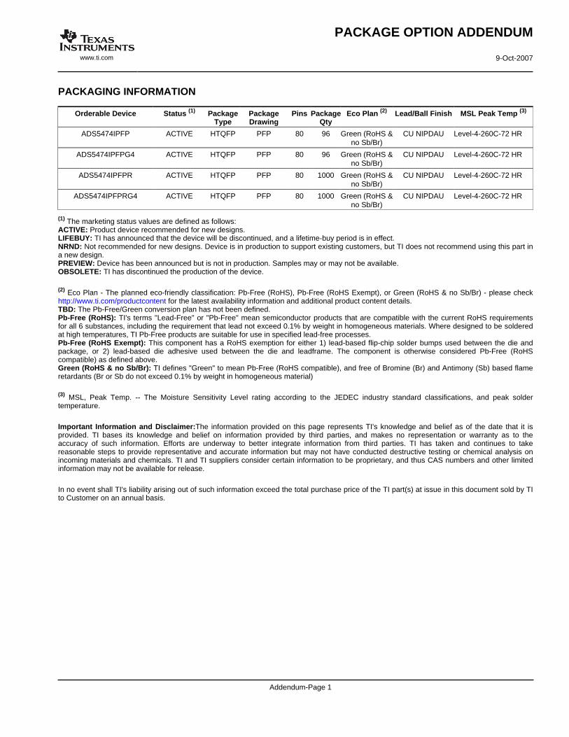
PACKAGING INFORMATION
Orderable Device Status (1) PackageType
PackageDrawing
Pins PackageQty
Eco Plan (2) Lead/Ball Finish MSL Peak Temp (3)
ADS5474IPFP ACTIVE HTQFP PFP 80 96 Green (RoHS &no Sb/Br)
CU NIPDAU Level-4-260C-72 HR
ADS5474IPFPG4 ACTIVE HTQFP PFP 80 96 Green (RoHS &no Sb/Br)
CU NIPDAU Level-4-260C-72 HR
ADS5474IPFPR ACTIVE HTQFP PFP 80 1000 Green (RoHS &no Sb/Br)
CU NIPDAU Level-4-260C-72 HR
ADS5474IPFPRG4 ACTIVE HTQFP PFP 80 1000 Green (RoHS &no Sb/Br)
CU NIPDAU Level-4-260C-72 HR
(1) The marketing status values are defined as follows:ACTIVE: Product device recommended for new designs.LIFEBUY: TI has announced that the device will be discontinued, and a lifetime-buy period is in effect.NRND: Not recommended for new designs. Device is in production to support existing customers, but TI does not recommend using this part ina new design.PREVIEW: Device has been announced but is not in production. Samples may or may not be available.OBSOLETE: TI has discontinued the production of the device.
(2) Eco Plan - The planned eco-friendly classification: Pb-Free (RoHS), Pb-Free (RoHS Exempt), or Green (RoHS & no Sb/Br) - please checkhttp://www.ti.com/productcontent for the latest availability information and additional product content details.TBD: The Pb-Free/Green conversion plan has not been defined.Pb-Free (RoHS): TI's terms "Lead-Free" or "Pb-Free" mean semiconductor products that are compatible with the current RoHS requirementsfor all 6 substances, including the requirement that lead not exceed 0.1% by weight in homogeneous materials. Where designed to be solderedat high temperatures, TI Pb-Free products are suitable for use in specified lead-free processes.Pb-Free (RoHS Exempt): This component has a RoHS exemption for either 1) lead-based flip-chip solder bumps used between the die andpackage, or 2) lead-based die adhesive used between the die and leadframe. The component is otherwise considered Pb-Free (RoHScompatible) as defined above.Green (RoHS & no Sb/Br): TI defines "Green" to mean Pb-Free (RoHS compatible), and free of Bromine (Br) and Antimony (Sb) based flameretardants (Br or Sb do not exceed 0.1% by weight in homogeneous material)
(3) MSL, Peak Temp. -- The Moisture Sensitivity Level rating according to the JEDEC industry standard classifications, and peak soldertemperature.
Important Information and Disclaimer:The information provided on this page represents TI's knowledge and belief as of the date that it isprovided. TI bases its knowledge and belief on information provided by third parties, and makes no representation or warranty as to theaccuracy of such information. Efforts are underway to better integrate information from third parties. TI has taken and continues to takereasonable steps to provide representative and accurate information but may not have conducted destructive testing or chemical analysis onincoming materials and chemicals. TI and TI suppliers consider certain information to be proprietary, and thus CAS numbers and other limitedinformation may not be available for release.
In no event shall TI's liability arising out of such information exceed the total purchase price of the TI part(s) at issue in this document sold by TIto Customer on an annual basis.
PACKAGE OPTION ADDENDUM
www.ti.com 9-Oct-2007
Addendum-Page 1

IMPORTANT NOTICETexas Instruments Incorporated and its subsidiaries (TI) reserve the right to make corrections, modifications, enhancements, improvements,and other changes to its products and services at any time and to discontinue any product or service without notice. Customers shouldobtain the latest relevant information before placing orders and should verify that such information is current and complete. All products aresold subject to TI’s terms and conditions of sale supplied at the time of order acknowledgment.TI warrants performance of its hardware products to the specifications applicable at the time of sale in accordance with TI’s standardwarranty. Testing and other quality control techniques are used to the extent TI deems necessary to support this warranty. Except wheremandated by government requirements, testing of all parameters of each product is not necessarily performed.TI assumes no liability for applications assistance or customer product design. Customers are responsible for their products andapplications using TI components. To minimize the risks associated with customer products and applications, customers should provideadequate design and operating safeguards.TI does not warrant or represent that any license, either express or implied, is granted under any TI patent right, copyright, mask work right,or other TI intellectual property right relating to any combination, machine, or process in which TI products or services are used. Informationpublished by TI regarding third-party products or services does not constitute a license from TI to use such products or services or awarranty or endorsement thereof. Use of such information may require a license from a third party under the patents or other intellectualproperty of the third party, or a license from TI under the patents or other intellectual property of TI.Reproduction of TI information in TI data books or data sheets is permissible only if reproduction is without alteration and is accompaniedby all associated warranties, conditions, limitations, and notices. Reproduction of this information with alteration is an unfair and deceptivebusiness practice. TI is not responsible or liable for such altered documentation. Information of third parties may be subject to additionalrestrictions.Resale of TI products or services with statements different from or beyond the parameters stated by TI for that product or service voids allexpress and any implied warranties for the associated TI product or service and is an unfair and deceptive business practice. TI is notresponsible or liable for any such statements.TI products are not authorized for use in safety-critical applications (such as life support) where a failure of the TI product would reasonablybe expected to cause severe personal injury or death, unless officers of the parties have executed an agreement specifically governingsuch use. Buyers represent that they have all necessary expertise in the safety and regulatory ramifications of their applications, andacknowledge and agree that they are solely responsible for all legal, regulatory and safety-related requirements concerning their productsand any use of TI products in such safety-critical applications, notwithstanding any applications-related information or support that may beprovided by TI. Further, Buyers must fully indemnify TI and its representatives against any damages arising out of the use of TI products insuch safety-critical applications.TI products are neither designed nor intended for use in military/aerospace applications or environments unless the TI products arespecifically designated by TI as military-grade or "enhanced plastic." Only products designated by TI as military-grade meet militaryspecifications. Buyers acknowledge and agree that any such use of TI products which TI has not designated as military-grade is solely atthe Buyer's risk, and that they are solely responsible for compliance with all legal and regulatory requirements in connection with such use.TI products are neither designed nor intended for use in automotive applications or environments unless the specific TI products aredesignated by TI as compliant with ISO/TS 16949 requirements. Buyers acknowledge and agree that, if they use any non-designatedproducts in automotive applications, TI will not be responsible for any failure to meet such requirements.Following are URLs where you can obtain information on other Texas Instruments products and application solutions:Products ApplicationsAmplifiers amplifier.ti.com Audio www.ti.com/audioData Converters dataconverter.ti.com Automotive www.ti.com/automotiveDSP dsp.ti.com Broadband www.ti.com/broadbandClocks and Timers www.ti.com/clocks Digital Control www.ti.com/digitalcontrolInterface interface.ti.com Medical www.ti.com/medicalLogic logic.ti.com Military www.ti.com/militaryPower Mgmt power.ti.com Optical Networking www.ti.com/opticalnetworkMicrocontrollers microcontroller.ti.com Security www.ti.com/securityRFID www.ti-rfid.com Telephony www.ti.com/telephonyRF/IF and ZigBee® Solutions www.ti.com/lprf Video & Imaging www.ti.com/video
Wireless www.ti.com/wireless
Mailing Address: Texas Instruments, Post Office Box 655303, Dallas, Texas 75265Copyright © 2008, Texas Instruments Incorporated
Related Documents