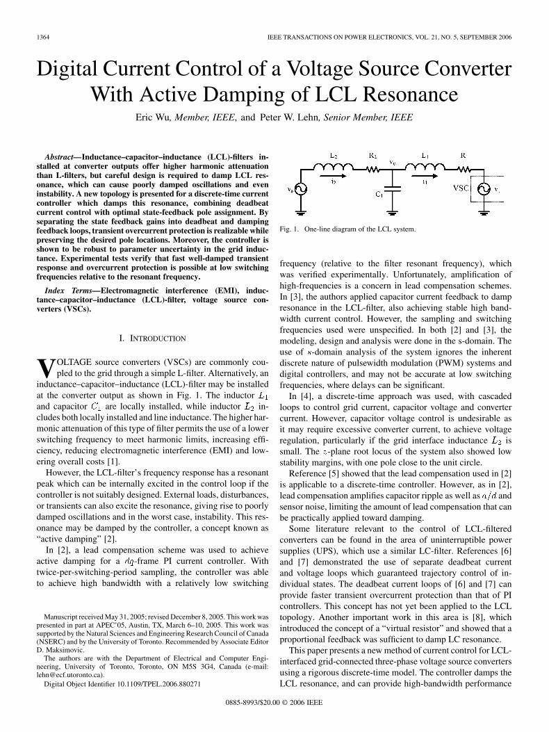
1364 IEEE TRANSACTIONS ON POWER ELECTRONICS, VOL. 21, NO. 5, SEPTEMBER 2006 Digital Current Control of a Voltage Source Converter With Active Damping of LCL Resonance Eric Wu, Member, IEEE, and Peter W. Lehn, Senior Member, IEEE Abstract—Inductance–capacitor–inductance (LCL)-filters in- stalled at converter outputs offer higher harmonic attenuation than L-filters, but careful design is required to damp LCL res- onance, which can cause poorly damped oscillations and even instability. A new topology is presented for a discrete-time current controller which damps this resonance, combining deadbeat current control with optimal state-feedback pole assignment. By separating the state feedback gains into deadbeat and damping feedback loops, transient overcurrent protection is realizable while preserving the desired pole locations. Moreover, the controller is shown to be robust to parameter uncertainty in the grid induc- tance. Experimental tests verify that fast well-damped transient response and overcurrent protection is possible at low switching frequencies relative to the resonant frequency. Index Terms—Electromagnetic interference (EMI), induc- tance–capacitor–inductance (LCL)-filter, voltage source con- verters (VSCs). I. INTRODUCTION V OLTAGE source converters (VSCs) are commonly cou- pled to the grid through a simple L-filter. Alternatively, an inductance–capacitor–inductance (LCL)-filter may be installed at the converter output as shown in Fig. 1. The inductor and capacitor are locally installed, while inductor in- cludes both locally installed and line inductance. The higher har- monic attenuation of this type of filter permits the use of a lower switching frequency to meet harmonic limits, increasing effi- ciency, reducing electromagnetic interference (EMI) and low- ering overall costs [1]. However, the LCL-filter’s frequency response has a resonant peak which can be internally excited in the control loop if the controller is not suitably designed. External loads, disturbances, or transients can also excite the resonance, giving rise to poorly damped oscillations and in the worst case, instability. This res- onance may be damped by the controller, a concept known as “active damping” [2]. In [2], a lead compensation scheme was used to achieve active damping for a -frame PI current controller. With twice-per-switching-period sampling, the controller was able to achieve high bandwidth with a relatively low switching Manuscript received May 31, 2005; revised December 8, 2005. This work was presented in part at APEC’05, Austin, TX, March 6–10, 2005. This work was supported by the Natural Sciences and Engineering Research Council of Canada (NSERC) and by the University of Toronto. Recommended by Associate Editor D. Maksimovic. The authors are with the Department of Electrical and Computer Engi- neering, University of Toronto, Toronto, ON M5S 3G4, Canada (e-mail: [email protected]). Digital Object Identifier 10.1109/TPEL.2006.880271 Fig. 1. One-line diagram of the LCL system. frequency (relative to the filter resonant frequency), which was verified experimentally. Unfortunately, amplification of high-frequencies is a concern in lead compensation schemes. In [3], the authors applied capacitor current feedback to damp resonance in the LCL-filter, also achieving stable high band- width current control. However, the sampling and switching frequencies used were unspecified. In both [2] and [3], the modeling, design and analysis were done in the s-domain. The use of -domain analysis of the system ignores the inherent discrete nature of pulsewidth modulation (PWM) systems and digital controllers, and may not be accurate at low switching frequencies, where delays can be significant. In [4], a discrete-time approach was used, with cascaded loops to control grid current, capacitor voltage and converter current. However, capacitor voltage control is undesirable as it may require excessive converter current, to achieve voltage regulation, particularly if the grid interface inductance is small. The -plane root locus of the system also showed low stability margins, with one pole close to the unit circle. Reference [5] showed that the lead compensation used in [2] is applicable to a discrete-time controller. However, as in [2], lead compensation amplifies capacitor ripple as well as and sensor noise, limiting the amount of lead compensation that can be practically applied toward damping. Some literature relevant to the control of LCL-filtered converters can be found in the area of uninterruptible power supplies (UPS), which use a similar LC-filter. References [6] and [7] demonstrated the use of separate deadbeat current and voltage loops which guaranteed trajectory control of in- dividual states. The deadbeat current loops of [6] and [7] can provide faster transient overcurrent protection than that of PI controllers. This concept has not yet been applied to the LCL topology. Another important work in this area is [8], which introduced the concept of a “virtual resistor” and showed that a proportional feedback was sufficient to damp LC resonance. This paper presents a new method of current control for LCL- interfaced grid-connected three-phase voltage source converters using a rigorous discrete-time model. The controller damps the LCL resonance, and can provide high-bandwidth performance 0885-8993/$20.00 © 2006 IEEE

Welcome message from author
This document is posted to help you gain knowledge. Please leave a comment to let me know what you think about it! Share it to your friends and learn new things together.
Transcript
1364 IEEE TRANSACTIONS ON POWER ELECTRONICS, VOL. 21, NO. 5, SEPTEMBER 2006
Digital Current Control of a Voltage Source ConverterWith Active Damping of LCL Resonance
Eric Wu, Member, IEEE, and Peter W. Lehn, Senior Member, IEEE
Abstract—Inductance–capacitor–inductance (LCL)-filters in-stalled at converter outputs offer higher harmonic attenuationthan L-filters, but careful design is required to damp LCL res-onance, which can cause poorly damped oscillations and eveninstability. A new topology is presented for a discrete-time currentcontroller which damps this resonance, combining deadbeatcurrent control with optimal state-feedback pole assignment. Byseparating the state feedback gains into deadbeat and dampingfeedback loops, transient overcurrent protection is realizable whilepreserving the desired pole locations. Moreover, the controller isshown to be robust to parameter uncertainty in the grid induc-tance. Experimental tests verify that fast well-damped transientresponse and overcurrent protection is possible at low switchingfrequencies relative to the resonant frequency.
Index Terms—Electromagnetic interference (EMI), induc-tance–capacitor–inductance (LCL)-filter, voltage source con-verters (VSCs).
I. INTRODUCTION
VOLTAGE source converters (VSCs) are commonly cou-pled to the grid through a simple L-filter. Alternatively, an
inductance–capacitor–inductance (LCL)-filter may be installedat the converter output as shown in Fig. 1. The inductorand capacitor are locally installed, while inductor in-cludes both locally installed and line inductance. The higher har-monic attenuation of this type of filter permits the use of a lowerswitching frequency to meet harmonic limits, increasing effi-ciency, reducing electromagnetic interference (EMI) and low-ering overall costs [1].
However, the LCL-filter’s frequency response has a resonantpeak which can be internally excited in the control loop if thecontroller is not suitably designed. External loads, disturbances,or transients can also excite the resonance, giving rise to poorlydamped oscillations and in the worst case, instability. This res-onance may be damped by the controller, a concept known as“active damping” [2].
In [2], a lead compensation scheme was used to achieveactive damping for a -frame PI current controller. Withtwice-per-switching-period sampling, the controller was ableto achieve high bandwidth with a relatively low switching
Manuscript received May 31, 2005; revised December 8, 2005. This work waspresented in part at APEC’05, Austin, TX, March 6–10, 2005. This work wassupported by the Natural Sciences and Engineering Research Council of Canada(NSERC) and by the University of Toronto. Recommended by Associate EditorD. Maksimovic.
The authors are with the Department of Electrical and Computer Engi-neering, University of Toronto, Toronto, ON M5S 3G4, Canada (e-mail:[email protected]).
Digital Object Identifier 10.1109/TPEL.2006.880271
Fig. 1. One-line diagram of the LCL system.
frequency (relative to the filter resonant frequency), whichwas verified experimentally. Unfortunately, amplification ofhigh-frequencies is a concern in lead compensation schemes.In [3], the authors applied capacitor current feedback to dampresonance in the LCL-filter, also achieving stable high band-width current control. However, the sampling and switchingfrequencies used were unspecified. In both [2] and [3], themodeling, design and analysis were done in the s-domain. Theuse of -domain analysis of the system ignores the inherentdiscrete nature of pulsewidth modulation (PWM) systems anddigital controllers, and may not be accurate at low switchingfrequencies, where delays can be significant.
In [4], a discrete-time approach was used, with cascadedloops to control grid current, capacitor voltage and convertercurrent. However, capacitor voltage control is undesirable asit may require excessive converter current, to achieve voltageregulation, particularly if the grid interface inductance issmall. The -plane root locus of the system also showed lowstability margins, with one pole close to the unit circle.
Reference [5] showed that the lead compensation used in [2]is applicable to a discrete-time controller. However, as in [2],lead compensation amplifies capacitor ripple as well as andsensor noise, limiting the amount of lead compensation that canbe practically applied toward damping.
Some literature relevant to the control of LCL-filteredconverters can be found in the area of uninterruptible powersupplies (UPS), which use a similar LC-filter. References [6]and [7] demonstrated the use of separate deadbeat currentand voltage loops which guaranteed trajectory control of in-dividual states. The deadbeat current loops of [6] and [7] canprovide faster transient overcurrent protection than that of PIcontrollers. This concept has not yet been applied to the LCLtopology. Another important work in this area is [8], whichintroduced the concept of a “virtual resistor” and showed that aproportional feedback was sufficient to damp LC resonance.
This paper presents a new method of current control for LCL-interfaced grid-connected three-phase voltage source convertersusing a rigorous discrete-time model. The controller damps theLCL resonance, and can provide high-bandwidth performance
0885-8993/$20.00 © 2006 IEEE
WU AND LEHN: DIGITAL CURRENT CONTROL OF A VOLTAGE SOURCE CONVERTER 1365
at relatively low switching frequencies. This new system allowsfor the flexible, systematic design approach of pole assignmentwhile retaining control of the current trajectory, providing tran-sient overcurrent protection even when the controller’s overallperformance criteria cannot be met [9].
II. SYSTEM MODELING
Assuming that the impedances of the three-phase system ofFig. 1 are balanced, the differential equations governing thethree-phase voltage and current vectors are
(1)
(2)
(3)
The three-phase vectors , , , , andin (1)–(3) can be replaced by complex space vectors , ,
, , and in the form by applyingthe amplitude-invariant Clarke transformation
(4)
and assuming no zero-sequence currents.The space-vectors may then be projected onto complex vari-
ables in the synchronously rotating -frameby performing the substitution on eachspace vector, with synchronous frequency . Assuming
0, the complex -frame differential equations are thengiven by
(5)
(6)
(7)
The subscripts will henceforth be dropped for convenience.Equations (5)–(7) can be now written in state-space form as
(8)
where
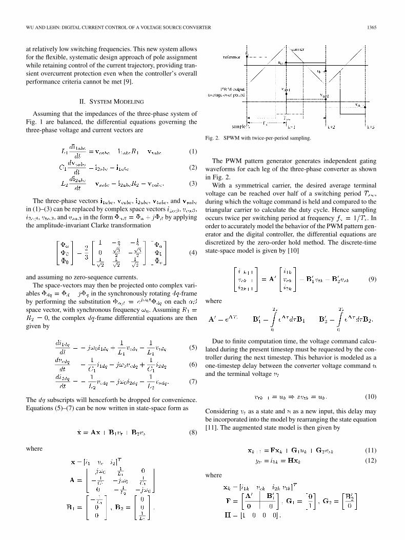
Fig. 2. SPWM with twice-per-period sampling.
The PWM pattern generator generates independent gatingwaveforms for each leg of the three-phase converter as shownin Fig. 2.
With a symmetrical carrier, the desired average terminalvoltage can be reached over half of a switching period ,during which the voltage command is held and compared to thetriangular carrier to calculate the duty cycle. Hence samplingoccurs twice per switching period at frequency 1 . Inorder to accurately model the behavior of the PWM pattern gen-erator and the digital controller, the differential equations arediscretized by the zero-order hold method. The discrete-timestate-space model is given by [10]
(9)
where
Due to finite computation time, the voltage command calcu-lated during the present timestep must be requested by the con-troller during the next timestep. This behavior is modeled as aone-timestep delay between the converter voltage commandand the terminal voltage
(10)
Considering as a state and as a new input, this delay maybe incorporated into the model by rearranging the state equation[11]. The augmented state model is then given by
(11)
(12)
where
1366 IEEE TRANSACTIONS ON POWER ELECTRONICS, VOL. 21, NO. 5, SEPTEMBER 2006
Fig. 3. Proposed complex current controller.
This complex-valued discrete-time state model will be used inthe control design and analysis which follows.
III. CONTROL DESIGN
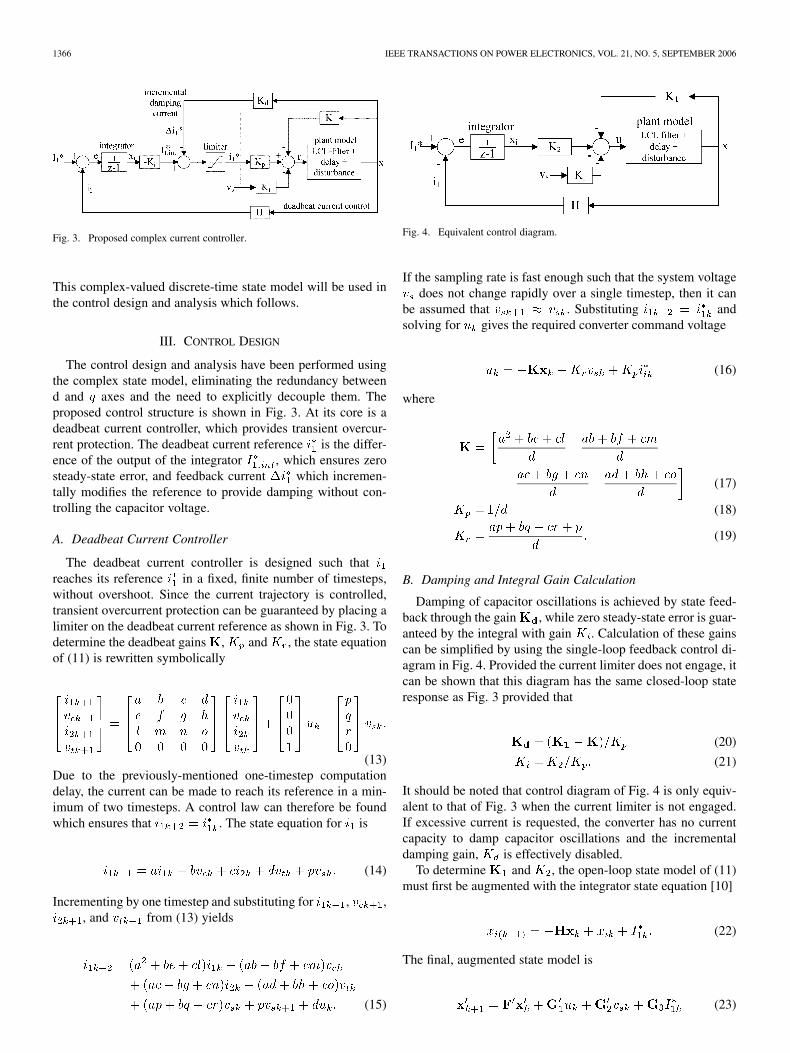
The control design and analysis have been performed usingthe complex state model, eliminating the redundancy betweend and axes and the need to explicitly decouple them. Theproposed control structure is shown in Fig. 3. At its core is adeadbeat current controller, which provides transient overcur-rent protection. The deadbeat current reference is the differ-ence of the output of the integrator , which ensures zerosteady-state error, and feedback current which incremen-tally modifies the reference to provide damping without con-trolling the capacitor voltage.
A. Deadbeat Current Controller
The deadbeat current controller is designed such thatreaches its reference in a fixed, finite number of timesteps,without overshoot. Since the current trajectory is controlled,transient overcurrent protection can be guaranteed by placing alimiter on the deadbeat current reference as shown in Fig. 3. Todetermine the deadbeat gains , and , the state equationof (11) is rewritten symbolically
(13)Due to the previously-mentioned one-timestep computationdelay, the current can be made to reach its reference in a min-imum of two timesteps. A control law can therefore be foundwhich ensures that . The state equation for is
(14)
Incrementing by one timestep and substituting for , ,, and from (13) yields
(15)
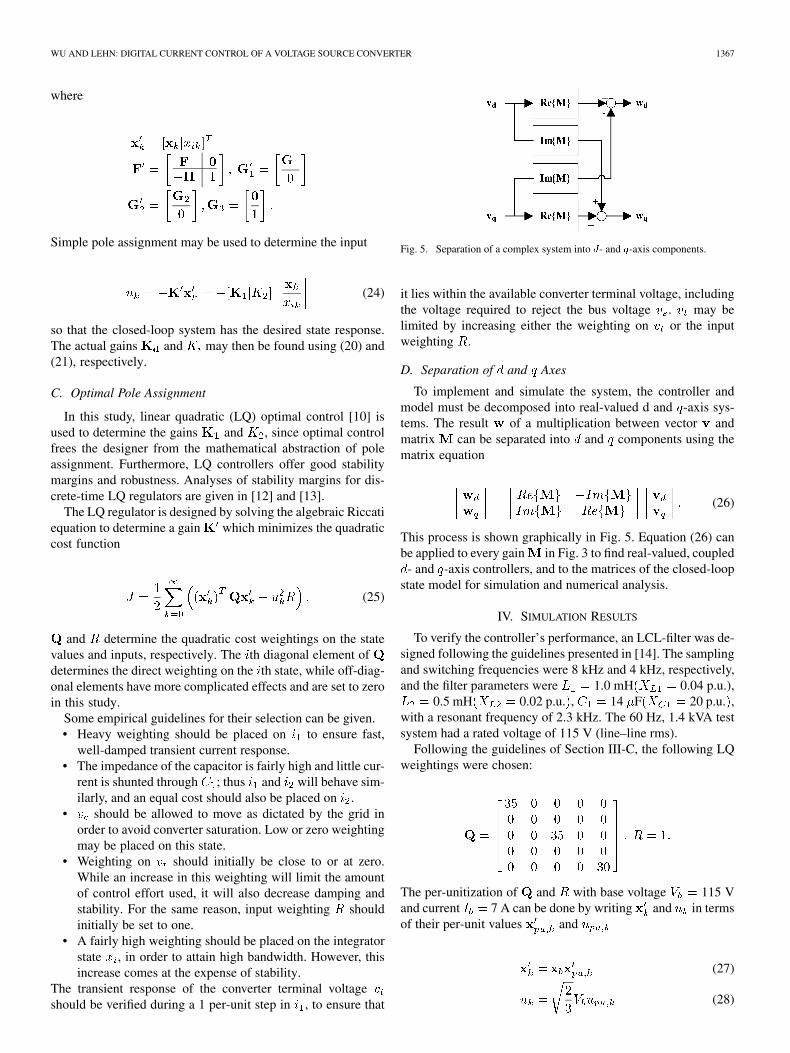
Fig. 4. Equivalent control diagram.
If the sampling rate is fast enough such that the system voltagedoes not change rapidly over a single timestep, then it can
be assumed that . Substituting andsolving for gives the required converter command voltage
(16)
where
(17)
(18)
(19)
B. Damping and Integral Gain Calculation
Damping of capacitor oscillations is achieved by state feed-back through the gain , while zero steady-state error is guar-anteed by the integral with gain . Calculation of these gainscan be simplified by using the single-loop feedback control di-agram in Fig. 4. Provided the current limiter does not engage, itcan be shown that this diagram has the same closed-loop stateresponse as Fig. 3 provided that
(20)
(21)
It should be noted that control diagram of Fig. 4 is only equiv-alent to that of Fig. 3 when the current limiter is not engaged.If excessive current is requested, the converter has no currentcapacity to damp capacitor oscillations and the incrementaldamping gain, is effectively disabled.
To determine and , the open-loop state model of (11)must first be augmented with the integrator state equation [10]
(22)
The final, augmented state model is
(23)
WU AND LEHN: DIGITAL CURRENT CONTROL OF A VOLTAGE SOURCE CONVERTER 1367
where
Simple pole assignment may be used to determine the input
(24)
so that the closed-loop system has the desired state response.The actual gains and may then be found using (20) and(21), respectively.
C. Optimal Pole Assignment
In this study, linear quadratic (LQ) optimal control [10] isused to determine the gains and , since optimal controlfrees the designer from the mathematical abstraction of poleassignment. Furthermore, LQ controllers offer good stabilitymargins and robustness. Analyses of stability margins for dis-crete-time LQ regulators are given in [12] and [13].
The LQ regulator is designed by solving the algebraic Riccatiequation to determine a gain which minimizes the quadraticcost function
(25)
and determine the quadratic cost weightings on the statevalues and inputs, respectively. The th diagonal element ofdetermines the direct weighting on the th state, while off-diag-onal elements have more complicated effects and are set to zeroin this study.
Some empirical guidelines for their selection can be given.• Heavy weighting should be placed on to ensure fast,
well-damped transient current response.• The impedance of the capacitor is fairly high and little cur-
rent is shunted through ; thus and will behave sim-ilarly, and an equal cost should also be placed on .
• should be allowed to move as dictated by the grid inorder to avoid converter saturation. Low or zero weightingmay be placed on this state.
• Weighting on should initially be close to or at zero.While an increase in this weighting will limit the amountof control effort used, it will also decrease damping andstability. For the same reason, input weighting shouldinitially be set to one.
• A fairly high weighting should be placed on the integratorstate , in order to attain high bandwidth. However, thisincrease comes at the expense of stability.
The transient response of the converter terminal voltageshould be verified during a 1 per-unit step in , to ensure that
Fig. 5. Separation of a complex system into d- and q-axis components.
it lies within the available converter terminal voltage, includingthe voltage required to reject the bus voltage . may belimited by increasing either the weighting on or the inputweighting .
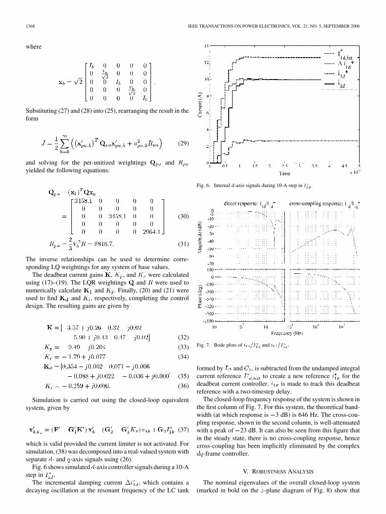
D. Separation of and Axes
To implement and simulate the system, the controller andmodel must be decomposed into real-valued d and -axis sys-tems. The result of a multiplication between vector andmatrix can be separated into and components using thematrix equation
(26)
This process is shown graphically in Fig. 5. Equation (26) canbe applied to every gain in Fig. 3 to find real-valued, coupled
- and -axis controllers, and to the matrices of the closed-loopstate model for simulation and numerical analysis.
IV. SIMULATION RESULTS
To verify the controller’s performance, an LCL-filter was de-signed following the guidelines presented in [14]. The samplingand switching frequencies were 8 kHz and 4 kHz, respectively,and the filter parameters were 1.0 mH 0.04 p.u.),
0.5 mH 0.02 p.u. , 14 F 20 p.u. ,with a resonant frequency of 2.3 kHz. The 60 Hz, 1.4 kVA testsystem had a rated voltage of 115 V (line–line rms).
Following the guidelines of Section III-C, the following LQweightings were chosen:
The per-unitization of and with base voltage 115 Vand current 7 A can be done by writing and in termsof their per-unit values and
(27)
(28)
1368 IEEE TRANSACTIONS ON POWER ELECTRONICS, VOL. 21, NO. 5, SEPTEMBER 2006
where
Substituting (27) and (28) into (25), rearranging the result in theform
(29)
and solving for the per-unitized weightings andyielded the following equations:
(30)
(31)
The inverse relationships can be used to determine corre-sponding LQ weightings for any system of base values.
The deadbeat current gains , , and were calculatedusing (17)–(19). The LQR weightings and were used tonumerically calculate and . Finally, (20) and (21) wereused to find and , respectively, completing the controldesign. The resulting gains are given by
(32)
(33)
(34)
(35)
(36)
Simulation is carried out using the closed-loop equivalentsystem, given by
(37)
which is valid provided the current limiter is not activated. Forsimulation, (38) was decomposed into a real-valued system withseparate - and -axis signals using (26).
Fig. 6 shows simulated -axis controller signals during a 10-Astep in .
The incremental damping current , which contains adecaying oscillation at the resonant frequency of the LC tank
Fig. 6. Internal d-axis signals during 10-A step in I .
Fig. 7. Bode plots of i =I and i =I .
formed by and , is subtracted from the undamped integralcurrent reference to create a new reference for thedeadbeat current controller. is made to track this deadbeatreference with a two-timestep delay.
The closed-loop frequency response of the system is shown inthe first column of Fig. 7. For this system, the theoretical band-width (at which response is 3 dB) is 646 Hz. The cross-cou-pling response, shown in the second column, is well-attenuatedwith a peak of 23 dB. It can also be seen from this figure thatin the steady state, there is no cross-coupling response, hencecross-coupling has been implicitly eliminated by the complex
-frame controller.
V. ROBUSTNESS ANALYSIS
The nominal eigenvalues of the overall closed-loop system(marked in bold on the -plane diagram of Fig. 8) show that
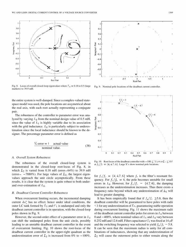
WU AND LEHN: DIGITAL CURRENT CONTROL OF A VOLTAGE SOURCE CONVERTER 1369
Fig. 8. Locus of overall closed-loop eigenvalues where L = 0.18 to 0.5 (largemarkers) to 39.9 mH.
the entire system is well-damped. Since a complex-valued state-space model was used, the pole locations are assymetrical aboutthe real axis, with each root actually representing a conjugatepair.
The robustness of the controller to parameter error was ana-lyzed by varying from the nominal design value of 0.5 mH,since the value of is highly variable due to its associationwith the grid inductance. is particularly subject to underes-timation since the local inductance should be known to the de-signer. The percentage parameter error is defined as
error actual valuenominal value
(38)
A. Overall System Robustness
The robustness of the overall closed-loop system isdemonstrated in the closed-loop root-locus of Fig. 8, inwhich is varied from 0.18 mH (error 64%) to 39.9 mH(error 7880%). For large values of , the largest eigen-values approach the unit circle asymptotically. From theseresults, it is clear that the system is quite robust to both under-and over-estimation of .
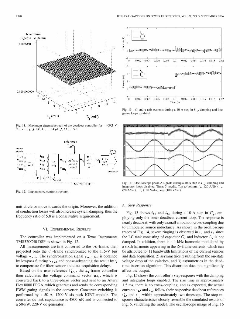
B. Deadbeat Current Controller Robustness
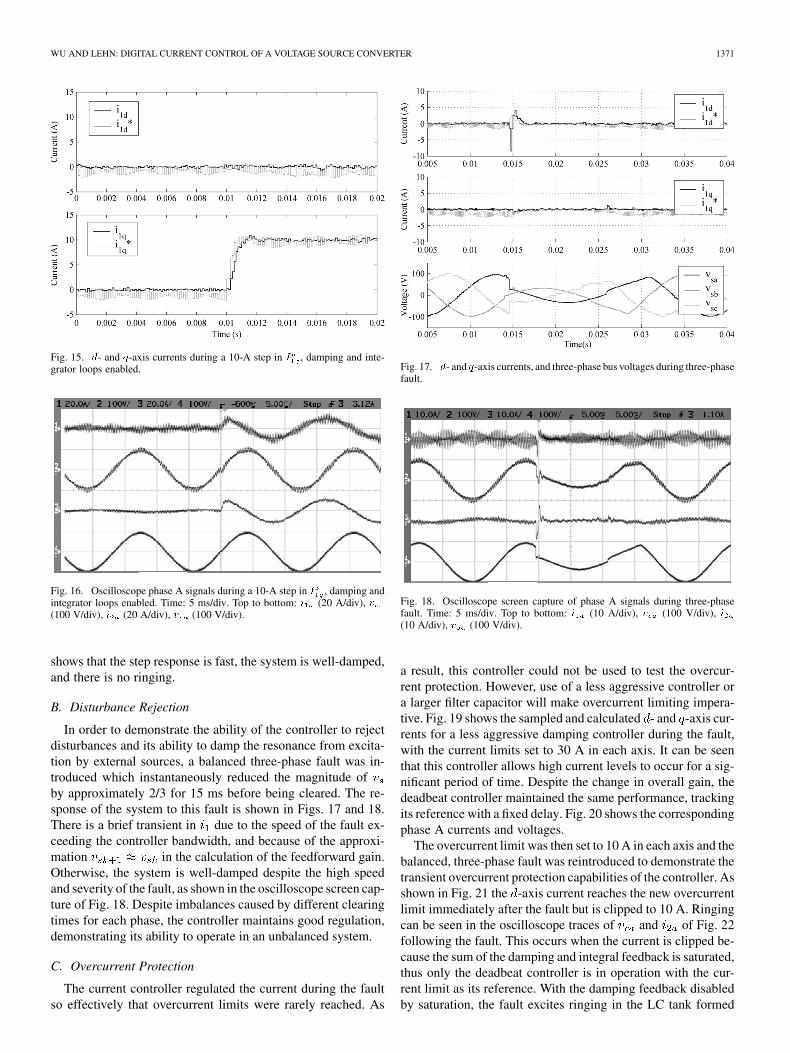
When overcurrent limiting occurs, the incremental dampingcurrent has no effect; hence under ideal conditions, theouter LC tank formed by and is undamped and only thedeadbeat current controller is in operation, with the closed-looppoles shown in Fig. 9.
However, the second-order effect of a parameter error incan shift the undamped poles from the unit circle, possiblyleading to an unstable deadbeat current controller in the eventof overcurrent limiting. Fig. 10 shows the root-locus of thedeadbeat current controller in the upper-right quadrant as theunderestimation error of is increased from 0% to 100%,
Fig. 9. Nominal pole locations of the deadbeat current controller.
Fig. 10. Root locus of the deadbeat controller with�100 � %errorL � 0%at f =f = f4; 4:7; 6g. Large X’s show nominal pole locations.
for where is the filter’s resonant fre-quency. For 4, the pole becomes unstable for smallerrors in . However, for , the dampingincreases as the underestimation increases. Thus there exists afrequency ratio beyond which any underestimation of willlead to greater damping.
It has been empirically found that if 5.8, then thedeadbeat controller will be guaranteed to have poles with radii
1 for any underestimation of , guaranteeing stable operationduring overcurrent limiting. Fig. 11 shows the maximum radiiof the deadbeat current controller poles for errors in between0 and 400%, where nominal values of and vary between0.252 mH and 12.6 mH. Filter capacitance was fixed at 14 Fand the switching frequency was selected to yield 5.8.It can be seen that the maximum radius is unity for all com-binations of inductances, showing that any underestimation of
will cause the outermost poles to either remain along the
1370 IEEE TRANSACTIONS ON POWER ELECTRONICS, VOL. 21, NO. 5, SEPTEMBER 2006
Fig. 11. Maximum eigenvalue radii of the deadbeat controller for �400% �
%errorL � 0%, C = 14 �F, f =f = 5.8.
Fig. 12. Implemented control structure.
unit circle or move towards the origin. Moreover, the additionof conduction losses will also increase system damping, thus thefrequency ratio of 5.8 is a conservative requirement.
VI. EXPERIMENTAL RESULTS
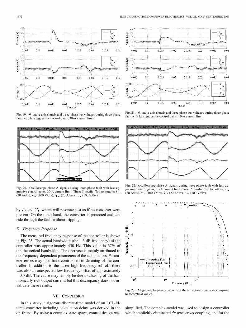
The controller was implemented on a Texas InstrumentsTMS320C40 DSP as shown in Fig. 12.
All measurements are first converted to the -frame, thenprojected onto the -frame synchronized to the 115-V busvoltage . The synchronization signal is obtainedby lowpass filtering and phase-advancing the result byto compensate for filter, sensor and data-acquisition delays.
Based on the user reference , the -frame controllerthen calculates the voltage command vector , which isconverted back to a three-phase vector and sent to an AlteraFlex 8000 FPGA, which generates and sends the correspondingPWM gating signals to the converter. Converter switching isperformed by a 50-A, 1200-V six-pack IGBT module. Theconverter dc link capacitance is 4800 F, and is connected toa 50-kW, 220-V dc generator.
Fig. 13. d- and q-axis currents during a 10-A step in i , damping and inte-grator loops disabled.
Fig. 14. Oscilloscope phase A signals during a 10-A step in i , damping andintegrator loops disabled. Time: 5 ms/div. Top to bottom: i (20 A/div), i(20 A/div), v (100 V/div), v (100 V/div).
A. Step Response
Fig. 13 shows and during a 10-A step in , em-ploying only the inner deadbeat current loop. The response isnearly deadbeat, with only a small amount of cross-coupling dueto unmodeled source inductance. As shown in the oscilloscopetraces of Fig. 14, severe ringing is observed in and sincethe LC tank consisting of capacitor and inductor is notdamped. In addition, there is a 4-kHz harmonic modulated bya sixth harmonic appearing in the -frame currents, which canbe attributed to: 1) bandwidth limitations of the current sensorsand data acquisition, 2) asymmetries resulting from the on-statevoltage drop of the switches, and 3) asymmetries in the dead-time insertion algorithm. This distortion does not significantlyaffect the output.
Fig. 15 shows the controller’s step response with the dampingand integrator loops enabled. The rise time is approximately1.5 ms, there is no cross-coupling, and as expected, the actualcurrents and follow their respective deadbeat references
and within approximately two timesteps. The step re-sponse characteristics closely resemble the simulated results ofFig. 6, validating the model. The oscilloscope image of Fig. 16
WU AND LEHN: DIGITAL CURRENT CONTROL OF A VOLTAGE SOURCE CONVERTER 1371
Fig. 15. d- and q-axis currents during a 10-A step in I , damping and inte-grator loops enabled.
Fig. 16. Oscilloscope phase A signals during a 10-A step in I , damping andintegrator loops enabled. Time: 5 ms/div. Top to bottom: i (20 A/div), v(100 V/div), i (20 A/div), v (100 V/div).
shows that the step response is fast, the system is well-damped,and there is no ringing.
B. Disturbance Rejection
In order to demonstrate the ability of the controller to rejectdisturbances and its ability to damp the resonance from excita-tion by external sources, a balanced three-phase fault was in-troduced which instantaneously reduced the magnitude ofby approximately 2/3 for 15 ms before being cleared. The re-sponse of the system to this fault is shown in Figs. 17 and 18.There is a brief transient in due to the speed of the fault ex-ceeding the controller bandwidth, and because of the approxi-mation in the calculation of the feedforward gain.Otherwise, the system is well-damped despite the high speedand severity of the fault, as shown in the oscilloscope screen cap-ture of Fig. 18. Despite imbalances caused by different clearingtimes for each phase, the controller maintains good regulation,demonstrating its ability to operate in an unbalanced system.
C. Overcurrent Protection
The current controller regulated the current during the faultso effectively that overcurrent limits were rarely reached. As
Fig. 17. d- and q-axis currents, and three-phase bus voltages during three-phasefault.
Fig. 18. Oscilloscope screen capture of phase A signals during three-phasefault. Time: 5 ms/div. Top to bottom: i (10 A/div), v (100 V/div), i(10 A/div), v (100 V/div).
a result, this controller could not be used to test the overcur-rent protection. However, use of a less aggressive controller ora larger filter capacitor will make overcurrent limiting impera-tive. Fig. 19 shows the sampled and calculated - and -axis cur-rents for a less aggressive damping controller during the fault,with the current limits set to 30 A in each axis. It can be seenthat this controller allows high current levels to occur for a sig-nificant period of time. Despite the change in overall gain, thedeadbeat controller maintained the same performance, trackingits reference with a fixed delay. Fig. 20 shows the correspondingphase A currents and voltages.
The overcurrent limit was then set to 10 A in each axis and thebalanced, three-phase fault was reintroduced to demonstrate thetransient overcurrent protection capabilities of the controller. Asshown in Fig. 21 the -axis current reaches the new overcurrentlimit immediately after the fault but is clipped to 10 A. Ringingcan be seen in the oscilloscope traces of and of Fig. 22following the fault. This occurs when the current is clipped be-cause the sum of the damping and integral feedback is saturated,thus only the deadbeat controller is in operation with the cur-rent limit as its reference. With the damping feedback disabledby saturation, the fault excites ringing in the LC tank formed
1372 IEEE TRANSACTIONS ON POWER ELECTRONICS, VOL. 21, NO. 5, SEPTEMBER 2006
Fig. 19. d- and q-axis signals and three-phase bus voltages during three-phasefault with less aggressive control gains, 30-A current limit.
Fig. 20. Oscilloscope phase A signals during three-phase fault with less ag-gressive control gains, 30-A current limit. Time: 5 ms/div. Top to bottom: i(20 A/div), v (100 V/div), i , (20 A/div), v (100 V/div).
by and , which will resonate just as if no converter werepresent. On the other hand, the converter is protected and canride through the fault without tripping.
D. Frequency Response
The measured frequency response of the controller is shownin Fig. 23. The actual bandwidth (the 3 dB frequency) of thecontroller was approximately 430 Hz. This value is 67% ofthe theoretical bandwidth. The decrease is mainly attributed tothe frequency-dependent parameters of the ac inductors. Param-eter errors may also have contributed to detuning of the con-troller. In addition to the faster high-frequency roll-off, therewas also an unexpected low frequency offset of approximately
0.5 dB. The cause may simply be due to aliasing of the har-monically rich output current, but this discrepancy does not in-validate these results.
VII. CONCLUSION
In this study, a rigorous discrete-time model of an LCL-fil-tered converter including calculation delay was derived in the
-frame. By using a complex state-space, control design was
Fig. 21. d- and q-axis signals and three-phase bus voltages during three-phasefault with less aggressive control gains, 10-A current limit.
Fig. 22. Oscilloscope phase A signals during three-phase fault with less ag-gressive control gains, 10-A current limit. Time: 5 ms/div. Top to bottom: i(20 A/div), v (100 V/div), i (20 A/div), v (100 V/div).
Fig. 23. Magnitude frequency response of the test system controller, comparedto theoretical values.
simplified. The complex model was used to design a controllerwhich implicitly eliminated -axes cross-coupling, and for the
WU AND LEHN: DIGITAL CURRENT CONTROL OF A VOLTAGE SOURCE CONVERTER 1373
first time combined the flexibility of pole assignment with in-herent transient overcurrent protection. -plane analysis of a testsystem with characteristic parameters showed that the controllerwas robustly stable to variations in the grid interface inductance.Both simulation and experimental results showed that even ata low switching frequency relative to the resonant frequency,the proposed control structure can achieve well-damped, high-bandwidth current control, and that cross-coupling can be min-imized. Furthermore, the controller has good disturbance rejec-tion, and regardless of overall performance provides instanta-neous overcurrent protection even during severe transient dis-turbances.
REFERENCES
[1] M. Lindgren and J. Svensson, “Connecting fast switching voltage-source converters to the grid-harmonic distortion and its reduction,”in Proc. IEEE/Stockholm Power Tech Conf., Stockholm, Sweden, Jun.1995, pp. 191–196.
[2] V. Blasko and V. Kaura, “A novel control to actively damp resonance ininput LC filter of a three-phase voltage source converter,” IEEE Trans.Ind. Appl., vol. 33, no. 2, pp. 542–550, Mar./Apr. 1997.
[3] E. Twining and D. Holmes, “Grid current regulation of a three-phasevoltage source inverter with an LCL input filter,” IEEE TransactionsPower Electron., vol. 18, no. 3, pp. 888–895, May 2003.
[4] M. Lindgren and J. Svensson, “Control of a voltage-source converterconnected to the grid through an LCL-filter-application to active fil-tering,” in Proc. Power Electron. Spec. Conf., Fukuoka, Japan, May1998, vol. 1, pp. 229–235.
[5] M. Liserre, A. Dell’Aquila, and F. Blaabjerg, “Stability improve-ments of an LCL-filter based three-phase active rectifier,” in Proc.Power Electron. Spec. Conf., Cairns, Australia, Jun. 2002, vol. 3, pp.1195–1201.
[6] T. Kawabata, T. Miyashita, and Y. Yamamoto, “Digital control of threephase PWM inverter with L-C filter,” in Proc. Power Electron. Spec.Conf., Kyoto, Japan, Apr. 1988, vol. 2, pp. 634–643.
[7] S. Buso, S. Fasolo, and P. Mattavelli, “Uninterruptible power supplymultiloop control employing digital predictive voltage and current reg-ulators,” IEEE Trans. Ind. Appl., vol. 37, no. 6, pp. 1846–1854, Nov./Dec. 2001.
[8] P. Dahono, Y. Bahar, Y. Sato, and T. Kataoka, “Damping of transientoscillations on the output LC filter of PWM inverters by using a virtualresistor,” in Proc. 4th IEEE Int. Conf. Power Electron. Drive Syst., Oct.2001, vol. 1, pp. 403–407.
[9] E. Wu and P. Lehn, “Digital current control of a voltage sourceconverter with active damping of LCL resonance,” in Proc. 20th Appl.Power Electron. Conf. Expo (APEC), Austin, TX, Mar. 2005, pp.1642–1649.
[10] G. F. Franklin, M. L. Workman, and D. J. Powell, Digital Control ofDynamic Systems, 2nd ed. Reading, MA: Addison-Wesley, 1990.
[11] O. Kukrer and H. Komurcugil, “Deadbeat control method for single-phase UPS inverters with compensation of computation delay,” Proc.Inst. Elect. Eng., pp. 123–128, Jan. 1999.
[12] A. T. Neto, J. Dion, and L. Dugard, “On the robustness of LQ regulatorsfor discrete time systems,” in Proc. 30th IEEE Conf. Decision Contr.,Brighton, UK, Dec. 1991, vol. 3, pp. 2960–2965.
[13] U. Shaked, “Guaranteed stability margins for the discrete-time linearquadratic optimal regulator,” IEEE Trans. Autom. Contr., vol. AC-31,no. 2, pp. 162–165, Feb. 1986.
[14] M. Liserre, F. Blaabjerg, and S. Hansen, “Design and control of anLCL-filter based three-phase active rectifier,” in Proc. 36th IAS Annu.Meeting, Chicago, IL, Oct. 2001, vol. 1, pp. 299–307.
Eric Wu (S’03–M’05) was born in Taipei, Taiwan, R.O.C., in 1978. He receivedthe B.A.Sc. and M.A.Sc. degrees in electrical engineering from the Universityof Toronto, Toronto, ON, Canada, in 2002 and 2005, respectively.
Peter W. Lehn (SM’05) received the B.Sc. and M.Sc. degrees in electrical en-ginnering from the University of Manitoba, Winnipeg, MB, Canada, in 1990and 1992, respectively, and the Ph.D. degree from the University of Toronto,Toronto, ON, Canada, in 1999.
From 1992 to 1994, he was with the Network Planning Group, Siemens AG,Erlangen, Germany. Presently, he is an Associate Professor at the University ofToronto.
Related Documents