12b 100MSps Pipeline ADC with Open-Loop Residue Amplifier A Major Qualifying Project Report: Submitted to the Faculty of WORCESTER POLYTECHNIC INSTITUTE In partial fulfillment of the requirements for the Degree of Bachelor of Science by ___________________________________ Devin Auclair ___________________________________ Charles Gammal ___________________________________ Fitzgerald Huang Submitted on: February 28, 2008 Approved: ___________________________________ Prof. John McNeill, PhD

Welcome message from author
This document is posted to help you gain knowledge. Please leave a comment to let me know what you think about it! Share it to your friends and learn new things together.
Transcript

12b 100MSps Pipeline ADC with Open-Loop Residue Amplifier
A Major Qualifying Project Report:
Submitted to the Faculty of
WORCESTER POLYTECHNIC INSTITUTE
In partial fulfillment of the requirements for the
Degree of Bachelor of Science
by
___________________________________
Devin Auclair
___________________________________ Charles Gammal
___________________________________
Fitzgerald Huang
Submitted on: February 28, 2008
Approved:
___________________________________ Prof. John McNeill, PhD
2007-2008 SRC/SIA IC Design Challenge Worcester Polytechnic Institute
Team 47 February 20, 2008
12b 100MSps Pipeline ADC with Open-Loop
Residue Amplifier
Team Leader: John McNeill
Students: Devin Auclair, Chuck Gammal, Jerry Huang
1
ABSTRACT The design of a low-power 12-bit 100MSps pipeline analog-to-digital converter (ADC) with
open-loop residue amplification using the novel “Split-ADC” architecture is described. The
choice of a 12b 100MSps specification targets medical applications such as portable ultrasound.
For a representative ADC such as the ADS5270, the figure of merit (FOM) is approximately
1pJ/step and the power dissipation is 113mW. The use of an open-loop residue amplifier
resulted in a FOM of 0.571pJ/step and a power dissipation of 11.2mW.

2
Table of Contents ABSTRACT .................................................................................................................................... 1
1 INTRODUCTION .................................................................................................................. 9
1.1 Introduction to Analog-to-Digital Converters .................................................................. 9
1.2 Quantization Error .......................................................................................................... 12
1.3 Types of ADCs ............................................................................................................... 13
1.3 ADC Performance Specifications .................................................................................. 15
1.4 Prior Work ...................................................................................................................... 17
1.5 Research Space and Goals .............................................................................................. 18
1.6 Background .................................................................................................................... 18
1.7 Purpose of Circuit ........................................................................................................... 19
1.8 High Performance Aspects ............................................................................................. 19
2 PIPELINED ADCs ............................................................................................................... 21
2.1 Architecture .................................................................................................................... 21
2.2 Operation ........................................................................................................................ 21
2.3 Pipelined ADC Performance Characteristics ................................................................. 25
3 BACKGROUND .................................................................................................................. 27
3.1 Karanicolas: Digital Self-Calibration Concept (1993) [4] ............................................. 27
3.2 Murmann: Open-loop residue amplification (2003) [10] ............................................... 29
3.3 Our Approach ................................................................................................................. 31
4 SYSTEM LEVEL DESIGN ................................................................................................. 32
4.1 System Block Diagram................................................................................................... 32
4.2 Design Methodology ...................................................................................................... 35
5 BEHAVIORAL SIMULATIONS ........................................................................................ 36
5.1 Open-Loop Residue Amplifier & MDAC ...................................................................... 36

3
5.2 Quantizer ........................................................................................................................ 37
5.3 Mode Select .................................................................................................................... 37
5.4 Pipeline ADC ................................................................................................................. 38
6 DETAILED CIRCUIT DESIGN .......................................................................................... 40
6.1 Open-Loop Residue Amplifier ....................................................................................... 40
6.1.1 Open-Loop Differential Amplifier .......................................................................... 40
6.1.2 Differential Pair with Passive Load ........................................................................ 42
6.1.3 Cascode ................................................................................................................... 42
6.1.4 Pi-Resistor Network ................................................................................................ 43
6.1.5 Amplifier Biasing.................................................................................................... 44
6.1.6 Transistor Sizing ..................................................................................................... 50
6.1.7 CMFB Design ......................................................................................................... 50
6.1.8 Replica Bias Design ................................................................................................ 52
6.1.9 Biasing Circuitry Design ......................................................................................... 54
6.1.10 Output Stage Design ............................................................................................... 55
6.1.11 Amplifier Schematic ............................................................................................... 62
6.2 MDAC ............................................................................................................................ 63
6.2.1 Theory of Operation ................................................................................................ 63
6.2.2 Capacitor Sizing ...................................................................................................... 65
6.2.3 MDAC Cell ............................................................................................................. 66
6.3 Quantizer ........................................................................................................................ 69
6.3.1 Number of Stages & Number of Bits per Stage ...................................................... 70
6.3.2 Track and Latch Comparator .................................................................................. 72
6.3.3 Preamplifier............................................................................................................. 73
6.3.4 Voltage References ................................................................................................. 74

4
6.3.5 Binary Encoder Design ........................................................................................... 76
7 TOP LEVEL CIRCUIT DESIGN ......................................................................................... 82
7.1 Floor Plan ....................................................................................................................... 82
7.2 Pad Ring ......................................................................................................................... 91
8 VERIFICATION................................................................................................................... 93
8.1 Open-Loop Residue Amplifier ....................................................................................... 93
8.1.1 Differential Gain and Output Swing ....................................................................... 93
8.1.2 Power Consumption ................................................................................................ 94
8.1.3 Overall Amplifier Specification .............................................................................. 96
8.2 MDAC ............................................................................................................................ 96
8.3 Quantizer ........................................................................................................................ 99
8.4 Phase Two Hardware Plan ........................................................................................... 100
9 Future Work ........................................................................................................................ 102
9.1 MDAC .......................................................................................................................... 102
9.2 Differential Amplifier .................................................................................................. 105
10 CONCLUSION ................................................................................................................... 107
11 REFERENCES ................................................................................................................... 108
APPENDIX A: MATLAB Uncorrelated ADC Simulator .......................................................... 109
APPENDIX B: INL/DNL Calculator ......................................................................................... 111
APPENDIX C: Verilog A Code ................................................................................................. 112
APPENDIX D: Behavioral Simulation Results .......................................................................... 119
APPENDIX E: Transistor Sizing Plots ....................................................................................... 131
APPENDIX F: 31-Level Quantizer Verification ........................................................................ 140

5
Table of Figures Figure 1: Analog v. Digital Signal .................................................................................................. 9
Figure 2: ADC Block Diagram [7] ............................................................................................... 10
Figure 3: Sampling ........................................................................................................................ 11
Figure 4: Nyquist-Shannon Sampling Theorem ........................................................................... 11
Figure 5: Quantization Error ......................................................................................................... 12
Figure 6: Ideal ADC Transfer Function ........................................................................................ 16
Figure 7: DNL Error greater and less than 1 LSB [2] ................................................................... 16
Figure 8. Integral Nonlinearity [2] ................................................................................................ 17
Figure 9: Pipelined ADC Block Diagram ..................................................................................... 21
Figure 10: Pipelined ADC Stage Block Diagram ......................................................................... 22
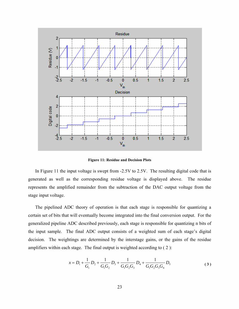
Figure 11: Residue and Decision Plots ......................................................................................... 23
Figure 12: Pipelined ADC Redundancy ....................................................................................... 24
Figure 13: Pipelined ADC Inherent Error Correction ................................................................... 25
Figure 14: Karanicolas' Digitally Self-Calibrating Scheme ......................................................... 28
Figure 15: Calibrating of Preceding Stages from Subsequent Stages ........................................... 29
Figure 16: Mode Select ................................................................................................................. 30
Figure 17: Redundant residue modes ............................................................................................ 31
Figure 18: System Block Diagram ................................................................................................ 32
Figure 19: Pipeline ADC Stage ..................................................................................................... 33
Figure 20: First Stage Critical Voltages ....................................................................................... 34
Figure 21: Subsequent Stage Critical Voltages ........................................................................... 34
Figure 22: Analog IC Design Flow ............................................................................................... 35
Figure 23: Open-Loop Residue Amplifier & MDAC Test Bench ................................................ 36
Figure 24: Quantizer Test Bench .................................................................................................. 37
Figure 25: Mode Select Test Bench .............................................................................................. 38
Figure 26: Stage Test Bench ......................................................................................................... 39
Figure 27: Pipelined ADC Stage - Differential Amplifier ............................................................ 40
Figure 28: Plot of Differential Input-Output Relation .................................................................. 41
Figure 29: Differential Pair with Passive Load ............................................................................. 42
Figure 30: Differential Pair with Passive Load and Cascode ....................................................... 43

6
Figure 31: Differential Pair with Passive Load, Cascode, and Pi-Resistor Network ................... 44
Figure 32: Half of Differential Pair Schematic ............................................................................. 45
Figure 33: 18u/0.18u NMOS Id-Vgs Characteristic ..................................................................... 47
Figure 34: Common-mode Current Equation Schematic .............................................................. 48
Figure 35: Tilted Differential Pair ................................................................................................ 48
Figure 36: Common-mode Feedback Concept ............................................................................. 51
Figure 37: Common-mode Feedback Circuit ............................................................................... 51
Figure 38: Replica Bias ................................................................................................................. 53
Figure 39: Biasing circuitry .......................................................................................................... 54
Figure 40: MDAC Capacitor Charge Path .................................................................................... 56
Figure 41: 40uA-biased Emitter Followers................................................................................... 57
Figure 42: 10MHz settling simulation, 40uA emitter-followers .................................................. 57
Figure 43: 100MHz settling simulation, 40uA emitter-followers ................................................ 58
Figure 44: 100MHz settling simulation, 160uA emitter-followers .............................................. 59
Figure 45: 100MHz settling simulation, 120uA emitter-followers .............................................. 60
Figure 46: 10MHz settling simulation, 120uA emitter-followers ................................................ 61
Figure 47: Final emitter-follower design ...................................................................................... 61
Figure 48: Differential Amplifier Schematic ................................................................................ 62
Figure 49: Pipelined ADC Stage - MDAC ................................................................................... 63
Figure 50: MDAC Theory of Operation ....................................................................................... 64
Figure 51: MDAC Theory of Operation – Phase One .................................................................. 64
Figure 52: MDAC Theory of Operation – Phase Two ................................................................. 64
Figure 53: MDAC Cell Schematic ................................................................................................ 66
Figure 54: MDAC Clocks ............................................................................................................. 68
Figure 55: MDAC Clock Generator Logic ................................................................................... 69
Figure 56: Pipeline ADC Stage: Quantizer ................................................................................... 69
Figure 57: Track and Latch Comparator Schematic ..................................................................... 72
Figure 58: Preamplifier Schematic ............................................................................................... 74
Figure 59: 31-Level Quantizer Voltage Levels ............................................................................ 75
Figure 60: 21-Level Quantizer Voltage Levels ............................................................................ 76
Figure 61: Typical Thermometer-to-Binary Encoder ................................................................... 77

7
Figure 62: Thermometer-to-Binary XOR Encoder with a "bubble" ............................................. 78
Figure 63: Fixed bubble via correction circuit .............................................................................. 79
Figure 64: Examples of thermometer-code bubbles ..................................................................... 79
Figure 65: Bubble Correction Block ............................................................................................. 80
Figure 66: Logic Diagram for Correction Circuit ......................................................................... 80
Figure 67: Quantizer Bubble-Correction Block (detail) ............................................................... 81
Figure 68: Bonding pad ................................................................................................................ 82
Figure 69: 2.4mm square die for ½ split ADC, with bonding pad/pad ring locations .................. 84
Figure 70: Quantizer and MDAC cell ........................................................................................... 85
Figure 71: Pipeline Stage Floorplan ............................................................................................. 86
Figure 72: ADC Stage Layout ...................................................................................................... 86
Figure 73: 80-pad Die with 1 ADC (1/2 split) .............................................................................. 87
Figure 74: Potential Pin Layout and Floor Plan for 80-Pad Die ................................................... 88
Figure 75: Potential Pin Layout and Floor Plan for 60-Pad Die ................................................... 89
Figure 76: Potential Pin Layout and Floor Plan for 62-Pad Die ................................................... 90
Figure 77: Proper Implementation of ESD Devices in custom Mixed-Signal IC ......................... 91
Figure 78: ESD cell ....................................................................................................................... 92
Figure 79: Cross-coupled ESD diodes and power supply clamp cells ......................................... 92
Figure 80: Some ESD cells in the pad ring ................................................................................... 92
Figure 81: DC sweep of Differential Amplifier ............................................................................ 93
Figure 82: DC Bias Rail and Resistive Dividers .......................................................................... 95
Figure 83: MDAC Verification Simulation .................................................................................. 98
Figure 84: 21-Level Single-Decision Quantizer Verification Simulation .................................... 99
Figure 85: Schedule of Layout Completion ................................................................................ 100
Figure 86: ADC IC with FPGA, PC, and Data Collection ......................................................... 101
Figure 87: MDAC Cell Operation - Capacitor Voltages ............................................................ 102
Figure 88: MDAC Cell Overall Switching Currents .................................................................. 103
Figure 89: Currents during Φ2 falling edge, Φ1A/Φ1 rising edges ............................................ 104
Figure 90: Currents during Φ1A/Φ1 falling edges, Φ2 rising edge ............................................ 105
Figure 91: 31-Level Quantizer Verification ............................................................................... 141

8
Table of Tables Table 1: Types of ADCs ............................................................................................................... 13
Table 2: Design Specifications ..................................................................................................... 18
Table 3: Transistor Sizing Plots .................................................................................................... 50
Table 4: Biasing Circuitry Currents .............................................................................................. 54
Table 5: Clock Generator Logic Equations .................................................................................. 67
Table 6: First Stage – Number of Bits per Stage Analysis ........................................................... 72
Table 7: Subsequent Stage – Number of Bits per Stage Analysis ................................................ 72
Table 8: I/O Signals requiring at least one bond pad .................................................................... 83
Table 9: Required Die Area (per ADC) ........................................................................................ 84
Table 10: Current consumption .................................................................................................... 94
Table 11: Differential Amplifier Specification ............................................................................. 96
Table 12: MDAC Verification Simulation Summary (all voltages in mV) .................................. 97
Table 13: 31-Level Quantizer Verification ................................................................................. 140

9
1 INTRODUCTION The purpose of this project is to design a 12b 100MSps split pipelined analog-to-digital
converter in a 0.18µm BiCMOS Jazz Semiconductor process for a portable ultrasound
application.
1.1 Introduction to Analog-to-Digital Converters An analog-to-digital converter, abbreviated ADC, A/D, or A to D, is an electronic device that
converts analog signals to digital signals. An analog signal, shown in Figure 1 on the left, is a
piece of real-world information such as force, temperature, or pressure. The reason for
converting such a measurement to a discrete digital signal, shown in Figure 1 on the right, is so
that a computer can process, transmit, or store that piece of information. Cell phones, cameras,
and camcorders, are examples of devices that contain ADCs. An analog signal differs from a
digital signal in that an analog signal can take on any y-value whereas a digital signal can only
take on certain y-values.
Figure 1: Analog v. Digital Signal
Figure 2 shows a block diagram of an ADC. The input to the ADC, vIN, is an analog signal.
The output of the ADC, n, is a digital signal that is proportional to the input signal, vIN. The
proportionality factor is referred to as the reference voltage and is designated vREF in the block
diagram. The analog input cannot be converted to a digital output at every instance in time.
Rather, the analog input is converted to a digital output every Ts seconds. The inverse of Ts is
referred to as the sampling frequency and it provides an alternative measure for how often an
vIN
t
n
t
y
x
Analog Signal Digital Signal
vIN
t
n
t
y
x
Analog Signal Digital Signal

10
analog signal is converted into a digital signal. This transformation is the fundamental procedure
behind an analog-to-digital converter; an analog signal is converted into a digital form.
Figure 2: ADC Block Diagram [7]
Sampling Frequency
An analog signal is converted to a digital signal through sampling. Sampling refers to how
often a portion of the input voltage is converted into a digital number. Figure 3 displays the
concept of sampling. Each of the green lines represents an instance in time when a sample is
taken. When a sample is taken, the value of the input voltage is converted to a digital number.
For example, the second green vertical line indicates the second sample. The input voltage has a
certain value at the second sample. That value is converted into a digital representation which is
designated n2 on the figure. Keep in mind that n2 is proportional to the input voltage but is not
necessarily equal to the input voltage. The distance between samples (green lines), is denoted as
the sampling time, Ts. The sampling time is related to the sampling frequency by the
relationship shown in Figure 2. The sampling frequency is a performance specification of all
ADC’s and is designated speed. How often do you need to sample to obtain a digital signal that
accurately represents the original analog signal?

11
Figure 3: Sampling
The answer to this question is in the Nyquist-Shannon sampling theorem; the theorem says
that you can reconstruct an analog signal completely if you sample the analog signal two times
faster than the largest frequency component in the analog signal. Figure 4 displays the
fundamental principle behind the Nyquist-Shannon sampling theorem. The figure shows a plot
of the frequency components of the input signal. The highest frequency component in the input
signal is denoted fh. Therefore, the appropriate sampling frequency, fs, is equal to 2fh, as indicated
in the figure.
Figure 4: Nyquist-Shannon Sampling Theorem
An important result of the Nyquist-Shannon Sampling Theorem is that you can reconstruct
an analog signal completely if you retain the value of the input voltage every time you take a
sample. This is not possible with an ADC because the output is a digital signal and a digital
t
vIN
n2
y
x
Ts
t
vIN
n2
y
x
Ts
f
X(f)
fh
fs = 2fh
f
X(f)
fh
fs = 2fh
f
X(f)
fh
fs = 2fh

12
signal can only take on certain y-values. The fact that a digital signal can only take on certain y-
values leads to a very important error in ADC’s called quantization error.
1.2 Quantization Error The principle of quantization error can be seen in Figure 5. The analog signal being
converted to a digital form is shown in blue. The possible output values of the ADC are
enumerated on the y-axis. A sample of the analog signal is taken at some point in time and is
denoted by the green line. The value of the input voltage (blue) at the time of the sample lies in
between the digital levels n2 and n3. Which level should be associated with that particular
sample? The level that should be associated with the sample is the level that is closest to the
original input voltage; in this case the level is n2. The original value of the input voltage differs
from level n2. The exact difference is denoted by the heavy black line in between level n2 and the
input voltage. This difference is called the quantization error and is an important limitation of all
ADC converters. The quantization error is a performance specification of all ADC’s and is
designated resolution.
Figure 5: Quantization Error
t
vin
n1
n2
n3
n4
n2or3
Quantization Error
y
x
y
x
t
vin
n1
n2
n3
n4
n2or3
Quantization Error
y
x
y
x

13
1.3 Types of ADCs There are three major categories of ADCs that are showcased in Table 1:
Low-to-medium speed & high accuracy
Medium speed & medium accuracy
High speed & low-to-medium accuracy
Table 1: Types of ADCs
Each of these categories of ADCs was investigated in order to find a suitable architecture for
the application of portable ultrasound. The 12b 100MSps specifications led to the selection of
a pipelined ADC.
Low Speed, High Accuracy
At the low-speed, high-accuracy end of the spectrum are the integrating and sigma-delta
oversampling ADCs. The integrating ADC, also known as a single-slope, dual-slope, or multi-
slope ADC, uses at least one integrating operational amplifier and one comparator. For a single-
slope ADC, the analog input voltage is integrated and then compared to a known reference
voltage. The time required for the analog input voltage to exceed the reference voltage is
proportional to the input voltage itself. This time is measured by a binary counter that
continually counts during the integration.
In general, the integrating ADC requires 2N clock cycles to obtain N bits of resolution. For a
12-bit integrating ADC, 212 = 4096 clock cycles are required. To obtain higher resolution, more
integrating time is required. While such an architecture is useful for certain applications, the
prohibitive low speed of the integrating ADC makes it and other slower ADC architectures poor
choices for portable ultrasound.
14
Medium Speed, Medium Accuracy
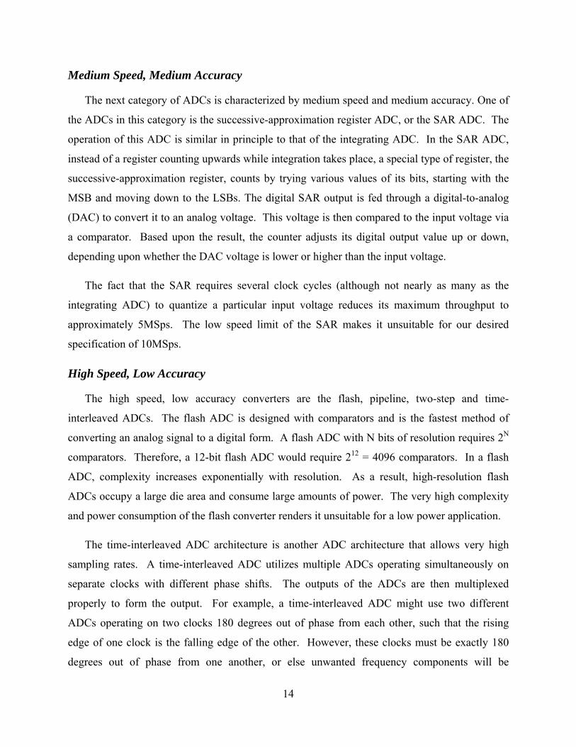
The next category of ADCs is characterized by medium speed and medium accuracy. One of
the ADCs in this category is the successive-approximation register ADC, or the SAR ADC. The
operation of this ADC is similar in principle to that of the integrating ADC. In the SAR ADC,
instead of a register counting upwards while integration takes place, a special type of register, the
successive-approximation register, counts by trying various values of its bits, starting with the
MSB and moving down to the LSBs. The digital SAR output is fed through a digital-to-analog
(DAC) to convert it to an analog voltage. This voltage is then compared to the input voltage via
a comparator. Based upon the result, the counter adjusts its digital output value up or down,
depending upon whether the DAC voltage is lower or higher than the input voltage.
The fact that the SAR requires several clock cycles (although not nearly as many as the
integrating ADC) to quantize a particular input voltage reduces its maximum throughput to
approximately 5MSps. The low speed limit of the SAR makes it unsuitable for our desired
specification of 10MSps.
High Speed, Low Accuracy
The high speed, low accuracy converters are the flash, pipeline, two-step and time-
interleaved ADCs. The flash ADC is designed with comparators and is the fastest method of
converting an analog signal to a digital form. A flash ADC with N bits of resolution requires 2N
comparators. Therefore, a 12-bit flash ADC would require 212 = 4096 comparators. In a flash
ADC, complexity increases exponentially with resolution. As a result, high-resolution flash
ADCs occupy a large die area and consume large amounts of power. The very high complexity
and power consumption of the flash converter renders it unsuitable for a low power application.
The time-interleaved ADC architecture is another ADC architecture that allows very high
sampling rates. A time-interleaved ADC utilizes multiple ADCs operating simultaneously on
separate clocks with different phase shifts. The outputs of the ADCs are then multiplexed
properly to form the output. For example, a time-interleaved ADC might use two different
ADCs operating on two clocks 180 degrees out of phase from each other, such that the rising
edge of one clock is the falling edge of the other. However, these clocks must be exactly 180
degrees out of phase from one another, or else unwanted frequency components will be

15
introduced into the multiplexed output. In addition, gain and offset error of the individual ADCs
needs to be corrected for, increasing the complexity of the time-interleaved ADC. The increased
complexity introduced due to multiple clocks resulted in our group not selecting the time-
interleaved ADC.
1.3 ADC Performance Specifications There are two key performance specifications of ADCs: differential nonlinearity and
integral nonlinearity.

16
Differential Nonlinearity
The differential nonlinearity (DNL) of an ADC is defined as the difference between the
actual step length and the ideal step length. An ideal transfer function for an ADC is displayed
in Figure 6. The y-axis displays the digital output values of the ADC and the x-axis displays the
analog input voltage values. The transfer characteristic is considered ideal because each of the
steps is of equal length. This characteristic is virtually impossible to realize in an ADC.
Figure 6: Ideal ADC Transfer Function
A desirable characteristic of ADCs is that of ‘no codes lost’. This refers to the ability of an
ADC to display all of the possible digital output codes sequentially. In terms of DNL, this
means a DNL of less than one LSB at any code. Figure 7 shows two cases: in the first, the DNL
error is less than 1 LSB and therefore no codes are lost.
Figure 7: DNL Error greater and less than 1 LSB [2]
17
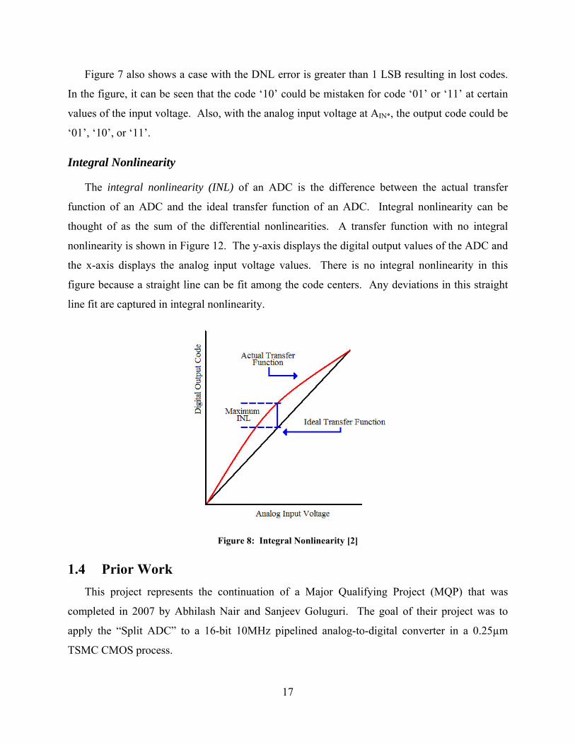
Figure 7 also shows a case with the DNL error is greater than 1 LSB resulting in lost codes.
In the figure, it can be seen that the code ‘10’ could be mistaken for code ‘01’ or ‘11’ at certain
values of the input voltage. Also, with the analog input voltage at AIN*, the output code could be
‘01’, ‘10’, or ‘11’.
Integral Nonlinearity
The integral nonlinearity (INL) of an ADC is the difference between the actual transfer
function of an ADC and the ideal transfer function of an ADC. Integral nonlinearity can be
thought of as the sum of the differential nonlinearities. A transfer function with no integral
nonlinearity is shown in Figure 12. The y-axis displays the digital output values of the ADC and
the x-axis displays the analog input voltage values. There is no integral nonlinearity in this
figure because a straight line can be fit among the code centers. Any deviations in this straight
line fit are captured in integral nonlinearity.
Figure 8: Integral Nonlinearity [2]
1.4 Prior Work This project represents the continuation of a Major Qualifying Project (MQP) that was
completed in 2007 by Abhilash Nair and Sanjeev Goluguri. The goal of their project was to
apply the “Split ADC” to a 16-bit 10MHz pipelined analog-to-digital converter in a 0.25µm
TSMC CMOS process.

18
1.5 Research Space and Goals The ADC designed in this project will be for a multichannel portable ultrasound system. The
requirements for such a device are lower power, high sampling rate, and high resolution. The
specifications for the ADC will be 100MSps and 12 bits. The project has been accepted into the
2007-2008 SRC/SIA (Semiconductor Research Corporation/Semiconductor Industry
Association) Design Challenge. The technology provided by the competition is a 0.18µm
BiCMOS Jazz Semiconductor process. The design specifications for the end product are
enumerated in Table 2.
Architecture Pipeline ADC Calibration Split ADC, Digital background Resolution 12b
Speed 100MSps Power ~50mW, 0.5pJ/step
SNR +70dB INL ±0.5LSB
Process 0.18μ, BiCMOS Jazz Semi
Table 2: Design Specifications
There is a comparable product currently on the market made by Texas Instruments. The
ADS5270 is a 12-bit, 40MSps, 8-channel ADC that has 113mW of power dissipation per ADC
and approximately 1pJ/step speed-power figure of merit (FOM). The goal of this project is to
increase performance with respect to power dissipation (50mW) and speed-power FOM
(0.5pJ/step).
1.6 Background The use of open-loop residue amplification in pipeline ADCs has been the subject of recent
investigation due to the power advantages over more precise closed-loop techniques, as well as
the general appeal of relaxing accuracy requirements on analog circuitry in deep submicron
CMOS. Due to the nonlinearity of the open-loop amplifier, digital calibration is used to restore
acceptable linear performance for the overall ADC. Previous work [10] has described
statistically based methods for determining the required calibration coefficients, which have the
drawback of relatively long adaptation times.

19
The “Split ADC” concept has been applied to correct linear gain errors in algorithmic and
pipeline ADCs [5], [8], and has the advantage of faster calibration convergence. Previous work
by an undergraduate project group working the in the team leader’s research lab [9] presented an
algorithm applying the split ADC approach to digital background correction of errors in pipeline
ADCs arising from the nonlinearity of open-loop residue amplifier stages. Compared with [10],
the novel contribution of this work is the dramatically reduced time for calibration convergence
by adopting the split ADC approach to correct amplifier nonlinearity errors, thereby making the
calibration of converters in the 14b to 16b range feasible.
The work completed describes the design of a mixed signal integrated circuit in Jazz
Semiconductor’s 180nm SiGe process to provide the analog functionality for a 12b, 100MSps,
pipeline ADC using open-loop residue amplifier gain stages. The nonlinearity of the open-
loop amplifier will be digitally corrected using a background calibration algorithm to be
implemented on an FPGA.
1.7 Purpose of Circuit The choice of a 12b 100MSps specification targets a performance space associated with
medical applications such as portable ultrasound. The 12b 100MSps combination represents a
balance between pushing extremes of high performance, while choosing a scope of project
reasonable for design and test in the time constraints given.
1.8 High Performance Aspects Speed-Power Figure of Merit (FOM) - Rather than push absolute limits, we have chosen a
target in an important application space with moderate speed and resolution; the high
performance aspect of the design will be the improvement in the speed-power FOM. For a
representative ADC such as the ADS5270 [13], the FOM is approximately 1 pJ/step; in addition,
the power dissipation in one ADC is 113mW. Through the use of an open-loop residue amplifier
we achieved sufficient power savings to improve the FOM to 0.571pJ/step and the power
dissipation in one ADC to 11.2mW. The details of the analysis of the FOM and power
dissipation can be found in section 8.1.2 titled Power Consumption.
Use of bipolar devices in residue amplifier stage – The output resistance of the residue
amplifier proved to be too large to drive the MDAC of the following stage. In order to achieve

20
further power savings in the residue amplifier stage, we selected a BJT emitter-follower to
interface between the residue amplifier and the MDAC. The details of the BJT emitter-follower
design are described in the Circuit Design section under Open-Loop Residue Amplifier.

21
2 PIPELINED ADCs This section will describe the architecture, operation, and performance considerations of a
pipelined ADC.
2.1 Architecture The pipelined is a popular architecture for modern applications of analog-to-digital
converters due to its high sustained sampling rate, low power consumption, and linear scaling of
complexity. Figure 9 shows a block diagram of a pipelined ADC. The term “pipelined” refers to
the stage-by-stage processing of an input sample VIN.
Figure 9: Pipelined ADC Block Diagram
In the above diagram, the analog input voltage VIN enters the ADC. Each subsequent
pipeline stage of the ADC resolves a certain n number of bits to be contributed to the final
conversion output. The number of bits that each stage is responsible for quantizing is usually on
the order of 1 – 5 bits. Simultaneously, after each stage has finished quantizing its input sample
to n bits, it outputs an analog residue voltage that serves as the input to the next stage. After s
stages of conversion, an m-bit ADC resolves the lower bits of the overall ADC digital output.
Each stage’s digital decision is then passed to a digital block that properly time-aligns the output
bits and corrects for any errors in each stage. The final digital decision is then produced.
2.2 Operation Each stage displayed in the block diagram shown above can be explored further. A typical
pipeline stage is displayed in Figure 10.

22
Figure 10: Pipelined ADC Stage Block Diagram
The input voltage is sampled and held in the sample-and-hold circuit embedded in each
stage. Subsequently, an n-bit flash ADC quantizes the analog voltage and produces a digital
decision of n bits. The digital decision is then fed through an n-bit flash DAC to be re-converted
into an analog signal. The summation node presented in the above diagram takes the input
voltage from the sample-and-hold circuit and subtracts the DAC voltage from it. This difference
voltage is then fed through a gain stage with gain G to produce the residue voltage, the output
voltage of this stage. In a typical pipelined ADC implementation, the sample-and-hold circuit
and flash DAC are typically implemented in a single switched-capacitor circuit called a
multiplying DAC, or MDAC. The amplification of the residue usually occurs with a closed-loop
operational amplifier, usually consisting of a differential input, gain stage, bias circuitry, and a
differential output stage.
In equation form, the output of each pipeline stage can be described as:
( 1 )
The residue voltage, VRES, becomes the input voltage to the next stage. The digital decisions
versus input voltage and the residues versus input voltage of a typical pipelined ADC are
displayed in Figure 11.
23
Figure 11: Residue and Decision Plots
In Figure 11 the input voltage is swept from -2.5V to 2.5V. The resulting digital code that is
generated as well as the corresponding residue voltage is displayed above. The residue
represents the amplified remainder from the subtraction of the DAC output voltage from the
stage input voltage.
The pipelined ADC theory of operation is that each stage is responsible for quantizing a
certain set of bits that will eventually become integrated into the final conversion output. For the
generalized pipeline ADC described previously, each stage is responsible for quantizing n bits of
the input sample. The final ADC output consists of a weighted sum of each stage’s digital
decision. The weightings are determined by the interstage gains, or the gains of the residue
amplifiers within each stage. The final output is weighted according to ( 2 ):
54321
4321
321
21
11111 D
GGGGD
GGGD
GGD
GDx ++++= ( 3 )

24
where Di and Gi represent the digital decision and the residue amplifier gain of each pipeline
stage. The above equation suggests that later stages have a smaller weight in the final ADC
output. This is indeed the case, as later stages resolve the lower bits of the overall conversion.
In the above example, D5 represents the digital decision made by the final flash ADC,
responsible for resolving the least significant bits of the output.
As mentioned before, each stage in a generalized pipelined ADC is responsible for resolving
n bits of the ADC output, while the final flash ADC is responsible for quantizing the m least
significant bits of the ADC output. It is evident from the serialized operation of the pipelined
ADC that some sort of time-alignment and error-correction circuitry is required for aligning each
stage’s digital decision to produce the final output.
Even though n bits are resolved by each stage and m bits resolved by the final ADC, the
maximum resolution of the ADC’s overall output is limited to s(n-1)+m where s is the number of
stages. There is a one-bit overlap of the digital decisions between adjacent pipelined stages. For
instance, a sample conversion may appear as follows:
S1: 0 0 1 S2: 0 1 0 S3: 0 0 0 S4: 0 1 1 S5: 0 1 1 0
= 0 0 1 1 0 0 0 1 1 1 1 0 Figure 12: Pipelined ADC Redundancy
The output bits of each stage are aligned in such a way that the LSB of one stage overlaps
with the MSB of the subsequent stage. The final ADC output is obtained when the columns are
added straight down, as shown. This provides a sort of inherent error correction. For example,
the output of stage 1 is 001. If the output of stage 1 had encountered an error and produced an
output of 000, the residue voltage out of stage 1 and into stage 2 would thus be higher. In
Equation 1 VDAC is the digital decision reconverted into an analog voltage via a DAC. If VDAC is
lower (000 fed through the DAC instead of a 001), then the resultant VRES will be higher. The
interstage gain factor G can be chosen such that the output of the next pipeline stage will
reproduce the missing 1 in its MSB. As such, the fact that stage 1 mistakenly produces a digital
decision of 000 (instead of 001) is counteracted by the fact that stage 2 will now produce a

25
digital decision of 110 (instead of 010). The final result of adding the results of these 2 stages’
digital outputs is:
S1: 0 0 0 S2: 1 1 0
0 0 1 1 0 Figure 13: Pipelined ADC Inherent Error Correction
Note that the inherent error correction produced by the one-bit overlaps enables the
overall added digital output to remain unchanged.
2.3 Pipelined ADC Performance Characteristics In general, the pipeline architecture enables the implementation of relatively high-resolution
ADCs without sacrificing processing speed or power draw. Additionally, the linear complexity
scaling inherent to the pipeline architecture makes the implementation of higher-resolution
pipeline ADCs more manageable than with another ADC architecture.
The architecture of the pipelined ADC enables it to have a high throughput rate. This is
evident in that pipelined ADCs can have sampling rates of a few MSps up to 100Msps+. The
reasoning for this is that the sample-and-hold circuit can begin processing the next analog input
voltage sample as soon as the DAC, summation node, and gain amplifier have finished
processing the previous sample. This pipelining action allows a high sustained sampling rate.
Additionally, since each stage is only responsible for quantizing a low number of bits relative to
the overall resolution of the pipeline ADC, each stage processes each sample relatively quickly.
The architecture of the pipelined ADC also allows it to scale linearly as complexity
increases. In the generalized pipeline ADC discussed earlier, each stage has a small flash ADC
that performs the quantization of the input sample. These flash ADCs are comprised of many
comparators that are responsible for quantizing the sample. For an n-bit flash ADC, 2n
comparators are needed to perform the conversion. In a pipeline ADC, higher overall resolution
is obtained effectively by adding additional small flash ADCs in the form of having more stages.
A 12-bit pipeline ADC with 4 stages, 3 bits per stage, and a 4-bit LSB flash ADC is implemented
using only 4(23)+24 = 48 comparators. This is in stark contrast to a 12-bit pure flash ADC,
which would require 212 = 4096 comparators in order to quantize the sample! The complexity in

26
a pipeline ADC scales linearly and not exponentially, as is the case in a flash ADC. It also
follows that fewer required comparators translates to much less power dissipation and power
draw, another advantage of the pipeline architecture.
Although the pipeline ADC allows for high speed, lower power dissipation, and low
complexity, there are still tradeoffs. For instance, the serialized nature of the conversion process
means that there is a significant time delay between the sample that enters the first sample-and-
hold of the first stage and when the digital alignment circuitry produces the correct output code.
Each stage in a pipeline ADC delays the data output by approximately one additional clock
cycle. This data latency has to be accounted for when implementing a pipelined ADC.
Even in spite of these tradeoffs, the pipelined ADC architecture enables an ADC to have
relatively high resolution, high speed, and low power dissipation, all with very few tradeoffs.

27
3 BACKGROUND
3.1 Karanicolas: Digital Self-Calibration Concept (1993) [4] In his paper, “A 15-b 1-Msample/s Digitally Self-Calibrated Pipeline ADC” published in the
IEEE JSSC 12/2003, Karanicolas describes a self-calibration scheme for a pipelined analog-to-
digital converter that attempts to compensate for errors such as capacitor mismatch, comparator
offset, charge injection, finite op-amp gain, and capacitor nonlinearity. Karanicolas employs a 1-
bit per stage, 17-stage design for his 15-bit pipelined ADC, noting that each stage is very simple
and fast, whose performance is limited only by the errors listed above.
Functionally, each stage compares its input to a reference voltage with a comparator to obtain
the single digital output bit. The residue voltage for each stage is passed through an amplifier to
the next stage. The ideal interstage gain in the presented ADC is nominally 2, accomplished by
closed-loop operational amplifiers. However, for the first 11 stages of Karanicolas’ ADC, he
employs an interstage gain of 1.93. The purpose behind this choice of gain is to ensure that the
residue voltage of each stage does not exceed the full scale range of the subsequent stage in a
worst case scenario (maximum capacitor mismatch, comparator offset, and charge injection error
magnitudes together). This gain reduction ensures that missing decision levels do not result from
the output of any stage exceeding the reference voltage. By doing so, the resulting missing codes
can be eliminated with digital calibration.
The digital calibration algorithm for a given stage requires the output residue voltage (VIN,
input to the current stage) and the output bit decision from the previous stage (DIN) as well as
two calibration constants S1 and S2 determined for that particular stage. Karanicolas cites the
eleventh stage for example:

28
Figure 14: Karanicolas' Digitally Self-Calibrating Scheme
Here, X refers to the uncorrected digital output, and Y refers to the corrected digital output.
The following describes the self-calibration algorithm:
Y = X if D = 0
Y = X + S1 – S2 if D = 1
S1 and S2 can be identified in the residue plot in Figure 14 where VIN = 0 with D = 0 and D =
1, respectively. S1 is determined when both the input voltage and the input digital decision are
both zero. S2 is determined when the input voltage is set to zero, but the input digital decision is
set to one. This transform ensures that the output code is the same when VIN = 0, no matter
whether D = 0 or D = 1, eliminating any missing codes resulting from any previously mentioned
errors.
From there, stage 11 is calibrated with the determining of constants S1 and S2. Stages 11-17
can be used in a similar manner to calibrate stage 10, as shown below:

29
Figure 15: Calibrating of Preceding Stages from Subsequent Stages
As such, the rest of the stages, stage one through nine, can be calibrated in a similar fashion.
The entire pipeline ADC is calibrated in this fashion. If this converter has a sample rate of
1Msps and 2,048 point averaging, the total calibration time is cited by Karanicolas to be about
70ms.
3.2 Murmann: Open-loop residue amplification (2003) [10] While the ubiquitous pipelined analog-to-digital converter boasts high sampling rates (10-
100MSps) and moderate resolution (12-16 bits), the typical pipelined ADC would not be the
premier choice in a portable ADC application. The typical pipelined ADC utilizes a precision
closed-loop operational amplifier to amplify the residue voltage that serves as the input to the
next stage, dominating the power dissipation of the entire ADC. This amplifier must meet
rigorous requirements in terms of speed, noise, and gain linearity. Murmann’s 2003 paper
explores the prospect of replacing this closed-loop amplifier with a simple open-loop differential
pair gain stage in the hope of reducing the power dissipation of a pipelined ADC.
Unfortunately, to replace the complex closed-loop amplifier with a simpler open-loop
differential stage results in a nonlinearity in the amplifier gain. Thus, Murmann also proposed a
digital background calibration technique to correct for this error in the digital domain, still
staying far below the power dissipation of a typical closed-loop amplifier implementation (60%
power savings). The general motivation for this approach to residue amplification is the result of

30
relaxing requirements on analog circuitry and moving that complexity into the digital domain,
where it can be more cheaply and efficiently implemented.
Murmann’s pipelined ADC utilized only one open-loop residue amplifier, in the most
critical multibit first stage. The nature of the pipelined ADC is such that errors in subsequent
stages (after the first stage) become less and less pronounced after each stage iteration. Although
subsequent stages still used the typical closed-loop amplifier implementation, Murmann’s work
also served as a vehicle to demonstrate that it would be almost trivial to implement this open-
loop amplifier and digital correction for every other stage.
By introducing an open-loop residue amplifier into the first stage of his ADC, Murmann
needed to correct for the nonlinear gain that would result. He does this by using a digital
background calibration technique that utilizes a digital lookup table calculated from measured
nonlinearity parameters pi. The parameter pi that characterizes the nonlinearity in the open-loop
amplifier can be determined by introducing a mode-select block into the pipeline stage block
diagram, enabling two different residue modes, as shown in the following diagram:
Figure 16: Mode Select
In Figure 16, the two residue modes are distinctly shown. The residue modes are controlled
by a single mode select bit labeled MODE that essentially shifts over the resulting residue plot
when MODE is enabled. The production of these two redundant residue modes is such that each
mode itself is capable of obtaining the conversion result correctly in the case of ideal operation.
The nonlinearity parameter pi can be estimated from the distances between the residues, as
shown in Figure 17.

31
Figure 17: Redundant residue modes
The residue differences h1 and h2 are measured to be the distances between the center and
near the edges of the residues, respectively. The difference between h1 and h2 is controlled by
nonlinearity parameter p2, where p2 increases with increasing nonlinearity of gain. The distances
h1 and h2 are measured by a statistics-based approach whose content is beyond the scope of this
project.
3.3 Our Approach In this project, we aim to apply concepts from both Karanicolas’ and Murmann’s work,
namely background calibration and open-loop residue amplification, respectively. Digital
background calibration shall enable us to utilize open-loop residue amplification in order for us
to further reduce power dissipation in our pipeline ADC architecture designed for a portable
ultrasound application.
32
4 SYSTEM LEVEL DESIGN The work described in the IC Block Diagram section includes a description of the system
block diagram and the design methodology used.
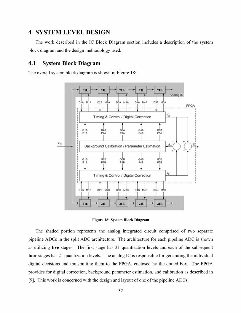
4.1 System Block Diagram The overall system block diagram is shown in Figure 18:
Figure 18: System Block Diagram
The shaded portion represents the analog integrated circuit comprised of two separate
pipeline ADCs in the split ADC architecture. The architecture for each pipeline ADC is shown
as utilizing five stages. The first stage has 31 quantization levels and each of the subsequent
four stages has 21 quantization levels. The analog IC is responsible for generating the individual
digital decisions and transmitting them to the FPGA, enclosed by the dotted box. The FPGA
provides for digital correction, background parameter estimation, and calibration as described in
[9]. This work is concerned with the design and layout of one of the pipeline ADCs.

33
Pipeline Stage
A block diagram for each pipeline ADC stage is shown in Figure 19. However, it should be
noted that the fifth stage will contain only a quantizer.
Figure 19: Pipeline ADC Stage
The input voltage is sampled and an ADC quantizes the analog voltage and produces a digital
decision (Q). Prior to the DAC conversion, the mode select will either (1) pass the digital
decision unchanged or (2) add one to the digital decision, similar to the RNG mechanism in [8]
and [10]. The DAC processes the digital decision and this decision is subtracted from the input
voltage. This differential voltage is then processed by the open-loop residue amplifier to
produce the residue voltage, the voltage that will serve as the input voltage to the next stage.
The ADC block will be realized by a flash converter. The S/H, mode select, DAC, and
summation node will be realized by an MDAC. Lastly, the gain stage will be realized by an
open-loop residue amplifier.
As in [9] and [10], the residue of each pipeline stage can be described as:
( 4 )
The above relation expresses the differential output as the differential input is subjected to a
linear gain G and a cubic error term that captures the nonlinearity in the differential pair.
As in [8] and [10], the stage is capable of operating in distinct residue modes as determined
by the mode select bit M. Due to the redundancy afforded by the choice of stage gain G and
ADC resolution, either residue mode will allow correct operation of the entire ADC. The key to

34
the split ADC concept is that use of different residue modes allows the two converters to proceed
along different decision trajectories.
Two different pipeline stages will be required in the design due to differences in the first and
subsequent stages. The first stage will need to process the input voltage from the portable
ultrasound machine. Subsequent stage inputs will be the output of the previous stage and
therefore will have the same signal swing. Figure 3 and Figure 21 show the critical voltage
swings for the first and subsequent stages.
Figure 20: First Stage Critical Voltages
Figure 21: Subsequent Stage Critical Voltages

35
4.2 Design Methodology Behavioral simulations preceded the transistor level design of the pipeline ADC. Using
Verilog-A, the entire pipeline ADC was simulated and verified. The transistor-level design
followed and verification was conducted by combining the behavioral Verilog-A blocks with
circuit-level simulation. Figure 22 shows the analog IC design flow for all phases of the project.
Figure 22: Analog IC Design Flow

36
5 BEHAVIORAL SIMULATIONS The work described in the Behavioral Simulations section includes the design of the open-
loop residue amplifier, MDAC, and quantizer in Verilog A. The performance of the ADC was
verified behaviorally before proceeding with the transistor level design.
5.1 Open-Loop Residue Amplifier & MDAC The open-loop residue amplifier and MDAC were designed as one behavioral block. The
purpose of the multiplying digital-to-analog converter (MDAC) is to subtract the analog
representation of the digital decision of the quantizer from the input signal (residue voltage) and
the purpose of the open-loop residue amplifier is to amplify the residue voltage. The input to the
MDAC and open-loop residue amplifier block is the differential input voltage of the stage, the
digital decision of the quantizer, possibly altered by the mode select, and the clock signal. The
output of the MDAC and open-loop residue amplifier block is the differential residue voltage.
The test bench for the open-loop residue amplifier and MDAC is shown in Figure 23.
Figure 23: Open-Loop Residue Amplifier & MDAC Test Bench
The block shown in the figure above samples the input, VIP and VIM, on the zero-crossings
of the falling edge of the clock (clk). The digital input (D) is converted to the analog voltage
levels (VDP and VDM). The analog voltage levels (VDP and VDM) are subtracted from the
sampled input (VIP and VIM) to produce the residue voltage. The residue voltage is then
amplified by a nonlinear gain, capturing the behavior of the open-loop residue amplifier, and

37
then outputted as VRP and VRM. The Verilog A code for the open-loop residue amplifier and
MDAC block can be found in APPENDIX C: Verilog A Code.
5.2 Quantizer The purpose of the quantizer is to convert the input signal from an analog signal to a digital
signal. The inputs to the quantizer are the differential input voltage (VIP and VIM) and the clock
signal. The output of the quantizer is the digital representation of the input voltage Q. The test
bench for the quantizer is shown in Figure 24.
Figure 24: Quantizer Test Bench
The block shown in the figure above samples the input, VIP and VIM, on the zero-crossings
of the falling edge of the clock (clk). The input voltage is then correlated to an appropriate value
Q which represents an approximation to the input voltage. The input voltage (VIP-VIM) shifts
from -1.5V to 1.5V. Appropriately, the quantizer approximates this input voltage on the zero-
crossings of the falling edge of the clock to produce the appropriate representations. The Verilog
A code for the quantizer can be found in APPENDIX C: Verilog A Code.
5.3 Mode Select The purpose of the mode select is to ensure that each ADC in the split-ADC architecture
takes a different path when converting an analog signal to a digital signal. Different paths are
ensured by the mode select. Prior to the DAC conversion, the mode select will either (1) pass the
digital decision unchanged or (2) add one to the digital decision. The inputs to the mode select
are the quantizer’s output Q and a bit M which specifies whether to pass the digital decision or

38
add one to the digital decision. The output of the mode select is the digital decision D. The test
bench for the mode select is shown in Figure 25.
The mode select is triggered by the bit M. A value of 0 for bit M results in the mode select
passing the input to the output unchanged. A value of 1 for bit M results in the mode select
adding one to the input Q to produce the output D. The Verilog A code for the mode select can
be found in APPENDIX C: Verilog A Code.
Figure 25: Mode Select Test Bench
5.4 Pipeline ADC The pipeline ADC was constructed by pipelining the stages shown in Figure 26. The residue
voltages of the first stage serve as the inputs for the subsequent stage. Four identical stages were
pipelined and the final “stage” consisted of a quantizer. The residue voltages (stages 1-4) and
output bits (20) for each stage were plotted and verified. The plots can be found in APPENDIX
D: Behavioral Simulation Results.

39
Figure 26: Stage Test Bench
40
6 DETAILED CIRCUIT DESIGN The work described in the Circuit Design section includes the design of the open-loop
residue amplifier, MDAC, and quantizer, including design equations and simulated results.
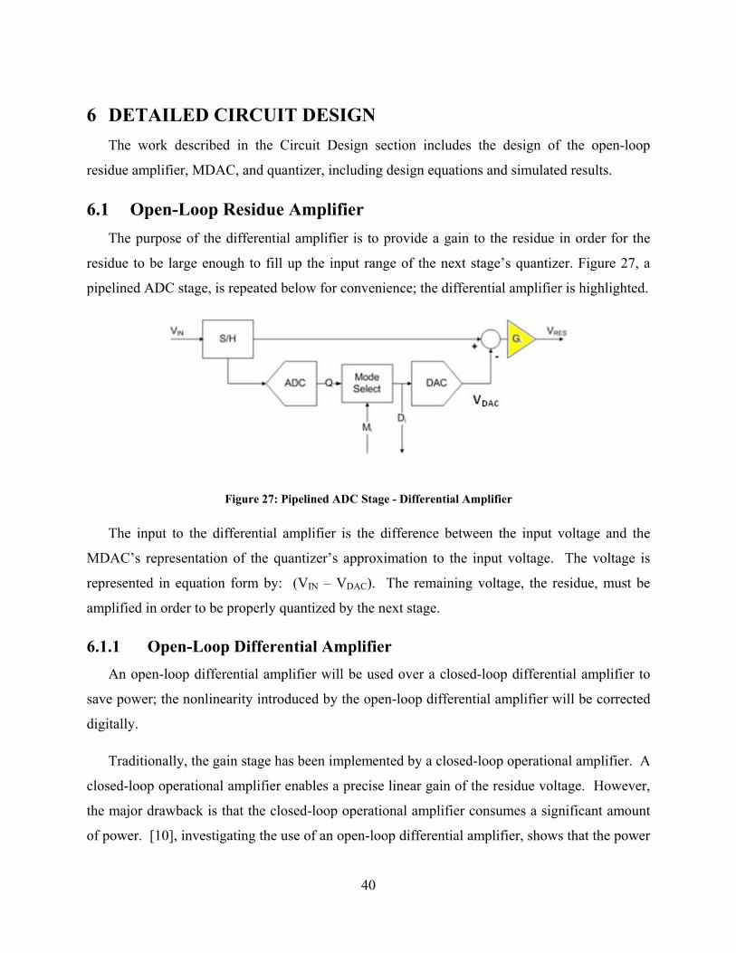
6.1 Open-Loop Residue Amplifier The purpose of the differential amplifier is to provide a gain to the residue in order for the
residue to be large enough to fill up the input range of the next stage’s quantizer. Figure 27, a
pipelined ADC stage, is repeated below for convenience; the differential amplifier is highlighted.
Figure 27: Pipelined ADC Stage - Differential Amplifier
The input to the differential amplifier is the difference between the input voltage and the
MDAC’s representation of the quantizer’s approximation to the input voltage. The voltage is
represented in equation form by: (VIN – VDAC). The remaining voltage, the residue, must be
amplified in order to be properly quantized by the next stage.
6.1.1 Open-Loop Differential Amplifier An open-loop differential amplifier will be used over a closed-loop differential amplifier to
save power; the nonlinearity introduced by the open-loop differential amplifier will be corrected
digitally.
Traditionally, the gain stage has been implemented by a closed-loop operational amplifier. A
closed-loop operational amplifier enables a precise linear gain of the residue voltage. However,
the major drawback is that the closed-loop operational amplifier consumes a significant amount
of power. [10], investigating the use of an open-loop differential amplifier, shows that the power
41
reduction of using an open-loop gain stage as opposed to a typical closed-loop amplifier is
around 60%, in a pipelined ADC design with a 3V supply. This power figure includes the
quantizer, biasing network, gain stage, and the digital post-processor. The major drawback of
the open-loop differential amplifier is that a nonlinear gain is applied to the residue voltage.
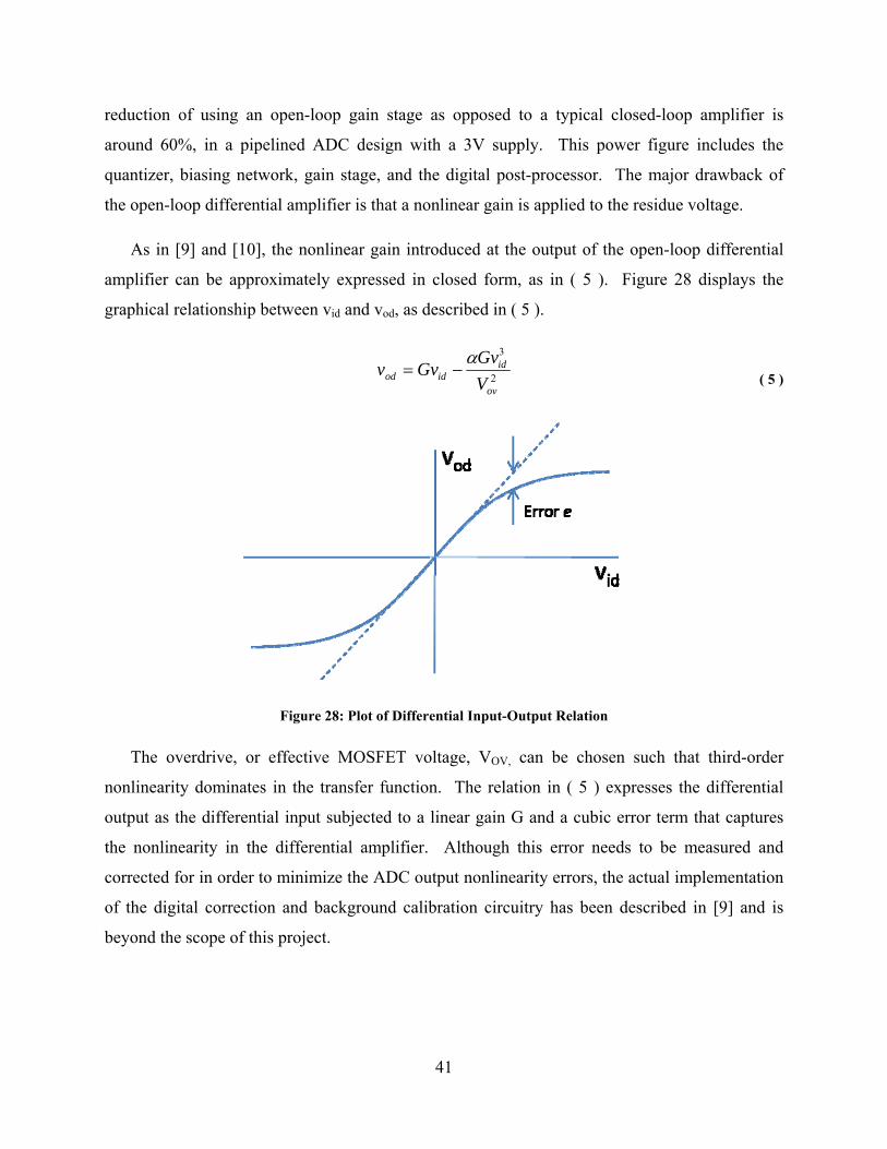
As in [9] and [10], the nonlinear gain introduced at the output of the open-loop differential
amplifier can be approximately expressed in closed form, as in ( 5 ). Figure 28 displays the
graphical relationship between vid and vod, as described in ( 5 ).
2
3
ov
ididod V
GvGvv
α−= ( 5 )
Figure 28: Plot of Differential Input-Output Relation
The overdrive, or effective MOSFET voltage, VOV, can be chosen such that third-order
nonlinearity dominates in the transfer function. The relation in ( 5 ) expresses the differential
output as the differential input subjected to a linear gain G and a cubic error term that captures
the nonlinearity in the differential amplifier. Although this error needs to be measured and
corrected for in order to minimize the ADC output nonlinearity errors, the actual implementation
of the digital correction and background calibration circuitry has been described in [9] and is
beyond the scope of this project.

42
6.1.2 Differential Pair with Passive Load We started the design of the differential amplifier by implementing a passively-loaded
differential pair circuit. The inputs to the differential amplifier are two differential signals. It is
required that the difference between the two signals be amplified. A differential pair was
selected as the appropriate topology for amplifying the difference between two signals.
The design of the pipeline ADC in the 0.18μm process is limited by a 1.8V supply. The low
voltage supply leaves little headroom between the supply voltage and ground. Therefore,
components that can support a small voltage drop are preferable in the load of the differential
pair. A resistive load, or passive load, was selected as the appropriate load for the differential
pair. A schematic of the differential pair with a passive load is shown in Figure 29.
Figure 29: Differential Pair with Passive Load
6.1.3 Cascode A cascode is inserted into the differential pair to prevent Miller multiplication of Cgd in M1
and M2.
There is a gate-drain capacitance that exists due to the geometry of the MOSFET. The Miller
effect describes how the gate-drain capacitance of the first stage will be amplified across a gain
stage. Note that in Figure 29 the drain node of M1 sees a gain. As a result, a transistor is

43
inserted between that node and M1 in order to buffer the gate-drain capacitance of the first stage
from being Miller multiplied. Similarly, a transistor is inserted between M2 and the resistor on
the right side of the differential pair. The resulting schematic is shown in Figure 30. The
cascode is represented by MOSFETs M3 and M4. It should be noted that a deep N well was
used in M1-M4 to tie the source to the body in order to eliminate the body effect.
Figure 30: Differential Pair with Passive Load and Cascode
6.1.4 Pi-Resistor Network A pi-resistor network is added to the differential pair in order to provide an extra degree of
freedom to control the gain of the amplifier without changing the common-mode as shown in
[10].
The pi-resistor network, shown in Figure 31, is inserted above M3 and M4. Additional
insight can be gained by analyzing the pi-resistor network using Bartlett’s bisection theorem.
Bartlett’s bisection theorem provides two circuit analysis techniques that show which circuit
components affect the common-mode voltages and currents and which circuit components affect
the differential mode voltages and currents.

44
To analyze those components that affect the common-mode, we open all leads between
points of symmetry. In terms of Figure 31, this means breaking the circuit between the two pi-
resistors. No current flows into either of the pi-resistors which leads to the conclusion that the
pi-resistors do not affect common-mode voltages and currents. To analyze the components that
affect the differential mode, we ground all leads between points of symmetry. In terms of Figure
31, this means inserting a ground between the two pi-resistors. The result is the observation that
the pi-resistor influences the differential mode voltages and currents.
Therefore, the pi-resistors provide a “knob” to adjust differential voltages and currents
without altering common-mode differential voltages and currents. The network will be
particularly useful when determining the gain of the differential amplifier.
Figure 31: Differential Pair with Passive Load, Cascode, and Pi-Resistor Network
6.1.5 Amplifier Biasing Using the structure in Figure 31, the differential amplifier was designed. The first step in the
analysis was to determine roughly how much voltage could be allocated to each of the
transistors. Figure 32 shows how we determined the appropriate allocation of voltage from the
supply voltage to ground. M3 is the cascode transistor, M1 is the input transistor, and M5 is the
45
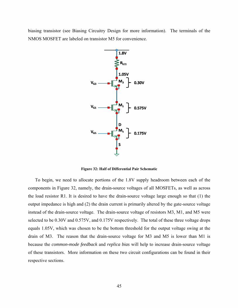
biasing transistor (see Biasing Circuitry Design for more information). The terminals of the
NMOS MOSFET are labeled on transistor M5 for convenience.
Figure 32: Half of Differential Pair Schematic
To begin, we need to allocate portions of the 1.8V supply headroom between each of the
components in Figure 32, namely, the drain-source voltages of all MOSFETs, as well as across
the load resistor R1. It is desired to have the drain-source voltage large enough so that (1) the
output impedance is high and (2) the drain current is primarily altered by the gate-source voltage
instead of the drain-source voltage. The drain-source voltage of resistors M3, M1, and M5 were
selected to be 0.30V and 0.575V, and 0.175V respectively. The total of these three voltage drops
equals 1.05V, which was chosen to be the bottom threshold for the output voltage swing at the
drain of M3. The reason that the drain-source voltage for M3 and M5 is lower than M1 is
because the common-mode feedback and replica bias will help to increase drain-source voltage
of these transistors. More information on these two circuit configurations can be found in their
respective sections.

46
For a symmetrical output voltage swing, the drain of MOSFET M3 needs to have a common-
mode voltage of 1.4V and needs to be able to swing up to 1.75V and down to 1.05V. Therefore,
the drain of resistor M3 will swing no lower than 1.05V. This voltage defines the available
drain-source voltages for transistors M3, M1, and M5.
Knowing the distribution of the 1.05V of drain-source voltage allows for the drain current
and transconductance of the differential amplifier to be calculated. The voltage at the drain of
transistor M5 is equal to the drain-source voltage of transistor M5 plus the voltage of ground.
The voltage at the drain of transistor M5 is set equal to 0.175V, for M5 will not need a
significant amount of drain-source voltage to remain properly biased due to the replica biasing
techniques used (see Replica Bias Design section). For the common-mode voltage on the gate of
M1, we choose a value of 0.9V, halfway between the supply rails. The gate-source voltage can
be calculated by subtracting the voltage at the drain of transistor M5 (0.175V) from the common-
mode voltage of M1 (900mV). The gate-source voltage of the input transistor M1 is thus
0.725V. Using a fixed W/L = 100 (18u/0.18u), we were able to produce a plot of drain current
and transconductance vs. gate-source voltage in Figure 33. Keep in mind that the simulation
performed in Figure 33 (drain-source voltage of 1V) served as a sufficiently accurate
approximation for the M1 drain-source voltage of 0.575V. From the curve on the left, the
threshold voltage was determined to be about 0.5V. Knowing the threshold voltage and gate-
source voltage, the effective voltage was calculated to be 0.225V. Using a gate-source voltage of
0.725V, the drain current was determined to be 1.0mA. Finally, using the gate-source voltage of
0.725V, the transconductance was determined to be 6.2mA/V.

47
Figure 33: 18u/0.18u NMOS Id-Vgs Characteristic
Three values need to be determined next: RLC, RLD, the series and pi load resistors, and ICM,
the common-mode feedback “helper” current; the desired values are shown in Figure 34. These
three values will help to define the rest of the differential amplifier. The gain of a differential
amplifier is generally given by ( 6 ), derived from the small-signal model of the MOSFET. The
load resistance in the differential amplifier design is given by the parallel combination of the
load resistor with the pi-resistor.
Gain = gm * RL = gm * (RLC || RLD) ( 6 )
gm is already known to be 6.2mA/V. We want to squeeze as much gain as possible out of the
amplifier, so we choose the desired gain of the amplifier to be 8 and will reduce the desired gain
if it proves unattainable.

48
Figure 34: Common-mode Current Equation Schematic
A second equation can be derived by analyzing Figure 34. The drain-current (ID3) is known
to be 1mA. The voltage drop across RLC is known to be 0.4V for a common-mode voltage of
1.4V. The total current flowing through the source of M1 is ID3-ICM (KCL). Given the
information provided, ( 7 ) can be written:
(1mA - ICM) RLC = 0.4V ( 7 )
Figure 35: Tilted Differential Pair

49
The third necessary equation can be obtained from “tilting” the differential pair and applying
circuit theory. Figure 35 shows the differential amplifier when VD1 has moved to its lowest point
(1.05V) and VD2 has moved to its highest point (1.75V). The tilted currents are determined by
taking the single-ended output voltage swing, dividing by the desired gain to obtain the
corresponding single-ended input voltage swing, and multiplying by the transconductance of the
differential input pair to obtain the current differential:
0.35
86.2
271.2 ( 8 )
1mA + 271.2uA = 1.27mA, and 1mA – 271.2uA = 0.73mA ( 9 )
Performing a KCL at the node represented by VD1 leads to ( 10 ):
0.75
RLC
0.7RLD
1.27 ICM ( 10 )
Solving ( 6 ), ( 7 ), and ( 10 ) leads to values for RLC, RLD, and ICM:
RLC = 1.284kΩ; RLD = 28kΩ; ICM = 688uA

50
6.1.6 Transistor Sizing Knowing the desired gain, the next step in the design of the differential amplifier was to
determine the W/L ratio. In order to determine the optimum ratio, an analysis of varying W/L
ratios was performed. The analysis consisted of plotting key voltages and currents in the circuit
in order to determine the optimum output resistance and transconductance, to name a few. The
plots analyzed, for both NMOS and PMOS transistors, are summarized in Table 3. In addition,
logarithmic plots of the dependent variable versus the independent variable were analyzed for all
five plots.
Plot Independent Variable Dependent Variable 1 Drain Current Gate-Source Voltage 2 Transconductance Gate-Source Voltage 3 Transconductance Drain Current 4 Drain Current Drain-Source Voltage 5 Drain-Source Resistance Drain-Source Voltage
Table 3: Transistor Sizing Plots
The W/L ratios plotted were: 18, 50, and 100 with a constant width of 18μm. Using a
differential pair, cascode, and resistor network (discussed previously), differential pairs were
designed with seven W/L ratios listed above for each transistor. The analysis showed that the
gain increases steadily with W/L up to 100. W/L’s greater than 100 lead to diminishing returns,
size increases no longer lead to gain increases. The result of this analysis led to a final selection
of a W/L of 100. Specifically the width of the transistor is 18μm, and the length of the transistor
is .18μm.
6.1.7 CMFB Design We also chose to include a common-mode feedback circuit into the design of the differential
amplifier. The CMFB concept is shown in Figure 36. The common-mode feedback circuitry
corrects for differences between the output common-mode voltage of the residue amplifier and
the desired common-mode voltage. In our application, the purpose of the CMFB circuit is to
ensure that the output common-mode of the differential amplifier stays at a constant 1.4V. By
doing so, the drain-source voltage of the cascoding devices can be maintained such that they
remain properly biased. This is accomplished via an actively loaded differential pair controlling

51
a pair of current sources that adjust the differential amplifier currents. Hence, a negative
feedback loop is formed.
Figure 36: Common-mode Feedback Concept
Figure 37: Common-mode Feedback Circuit
The inverting input of the CMFB differential pair is tied to the output common-mode
voltage, which is present in the middle of the pi-resistor load. Therefore, we choose to split the
pi-loaded resistor into two resistors, the point of connection between them containing the output
common-mode voltage.

52
The non-inverting input of the CMFB differential pair is tied to a resistive divider that
produces a reference voltage of 1.4V, the desired output common-mode of the differential
amplifier.
If the output common-mode drops below 1.4V, the CMFB differential pair will tilt and cause
the gate-source voltage of the CMFB current sources to increase, increasing the current fed into
the main differential pair. This will in turn cause the currents in the load resistors to decrease,
increasing the output common-mode to compensate. Conversely, the CMFB differential pair will
tilt in the opposite direction if the output common-mode increases to above 1.4V. This will
decrease the gate-source voltage of the CMFB current sources, decreasing the current fed into
the main differential pair. The current in the load resistors will thus increase, decreasing the
output common-mode to compensate.
6.1.8 Replica Bias Design The purpose of the replica biasing technique used in the design of this differential amplifier
is to ensure that the current source providing the bias current to the main differential pair remains
in the active region by replicating its operating point on another transistor. The replica biasing
technique used in the design of this differential amplifier involves a second MOSFET differential
pair, whose operating point can be accurately set. The schematic of the replica biasing circuit we
used is shown in Figure 38.

53
Figure 38: Replica Bias
The replica differential pair is biased with a PMOS cascode current mirror, which will be
described later in this section. The replica pair’s differential input, gates of M2 and M5, is
connected directly to the main differential pair’s differential input, the gates of M1 and M6.
Finally, the bias current for the replica pair is fed through an NMOS transistor M3, which in turn
mirrors the bias current for the main differential pair onto NMOS transistor M4.
When the differential input voltage swings to its extreme maximum, the inverting input of
the differential pair will be at its lowest voltage. Without a replica biasing technique, the drain-
source voltage of M4 will decrease, crashing M4 from the active region into the triode region,
which is catastrophic for the operation of the main amplifier.
Using the replica amplifier to bias the main amplifier results in a much more stable biasing
configuration. The 225uA current from the PMOS biasing circuitry (to be discussed later) will
always be biasing the replica amplifier, regardless of what the differential input to the amplifier
is. Since the replica amplifier ‘replicates’ the operating point of the main amplifier, there will
always be 225uA of current in M3. M4, the current source for the main amplifier, is mirrored off
of M3 but wider by a factor of about 8, producing the 2mA required for biasing the main
amplifier. Thus, this replica biasing technique provides a stable biasing scheme for the main
amplifier, regardless of the magnitude of the differential input voltage to the amplifier.

54
6.1.9 Biasing Circuitry Design For the biasing circuitry of this amplifier, we chose to use a series of cascoded current
mirrors. The biasing circuitry is shown in Figure 39, while a table of corresponding W/Ls and
currents provided by the biasing circuitry is enumerated in Table 4: Biasing Circuitry Currents
Bias current for: Mirror W/L (um) Current (uA) Main mirror NMOS 3.24/0.18 200 CMFB Differential Pair NMOS 1.62/0.18 85 NMOS to PMOS Mirroring -- 16.2/0.18 606.0 Replica bias PMOS 7.2/0.18 225.0 2 x CMFB helper currents PMOS 21.6/0.18 1520.0
Table 4: Biasing Circuitry Currents
Figure 39: Biasing circuitry
The main 200uA current is set by a 5.5kΩ resistor. NMOS and PMOS current mirrors are
then utilized with modified W/L ratios to set the proper bias currents for each section of
circuitry, as shown in Figure 39. Recall that our design required a large ICM CMFB “helper”
current of around 760uA per half-circuit that would allow the gain of the differential amplifier to
55
increase while maintaining a relatively high gm for the differential input pair. This CMFB
current is provided by the biasing circuitry, shown in Figure 39.
6.1.10 Output Stage Design As enumerated in the following MDAC design chapter, each MDAC cell uses a 50fF
capacitor to perform the subtraction operation required. In the first stage MDAC, there will be
31 MDAC cells per channel, one for each decision level of the first stage quantizer. This
represents a total capacitance of (50fF)(31) = 1550fF. Recall that the output resistance RO of the
differential amplifier is typically given by RO = RLC || RLD. This is approximately 1.6kΩ in our
design.
We must now ensure that the differential amplifier output is able to drive the MDAC
capacitors sufficiently such that we can operate at the desired 100MHz speed. As the MDAC
chapter enumerates, the phase φ2, where the charge on the capacitor is being ‘evaluated’, lasts
3.0ns, a significant constraint. To ensure proper interfacing of the differential amplifier and the
next stage’s input, we must see that the differential amplifier output is able to drive the
capacitive load of the next stage’s input within phase φ2. In other words, we must ensure that the
error at the output of the differential amplifier is within 1 LSB, referred back to the stage input
voltage.
For the first stage, this 1 LSB referred back to the stage input voltage is actually (2V/31)/8 =
8.06mV. For all subsequent stages, this value is (1.4V/21)/8 = 8.33mV. The error between the
actual voltage and the predicted voltage must be below these 1 LSB-referred error voltages. For
simplicity, we will choose the tighter-tolerance value of 8.06mV for all stages. If the first stage
output settling is adequate, then the output settling for all subsequent stages will also be
acceptable due to lesser capacitance at subsequent stage output nodes (only 21 levels vs. 31
levels in the first stage).
Using the 2.2 times the RC time constant of the charging circuit, we can estimate the length
of time required for the output to settle within 1 input-referred LSB. We know that the total
capacitance per MDAC cell is 50fF. Next, we select an arbitrary time constant, RC = 500ps, that
we assume will be small enough for the desired settling behavior (2.2RC = 1.1ns << φ2). We can
thus find the maximum series resistance R to achieve this settling behavior. 500ps/50fF = 10kΩ.

56
Figure 40: MDAC Capacitor Charge Path
Figure 40 shows a simplified schematic of the MDAC capacitor charge path. Essentially, the
differential amplifier’s output resistance is responsible for charging each 50fF capacitor through
two other resistances, an analog transmission gate series resistance, and another series switch
resistance. To attain the required 10kΩ series resistance in the charging path, we choose to size
the MDAC cell transmission gate and the second switch appropriately in order to obtain
approximately a 4.2kΩ RDS(on) for each (this turns out to be 3.6u/0.18u for NMOS and
14.4u/0.18u for PMOS). This should allow the output resistance of the differential amplifier to
charge the MDAC cell capacitors and allow the output to settle within the allotted period of φ2.
However, sizing the MDAC cell switches appropriately does not address the issue of settling
in its entirety. As it turns out, the differential amplifier output cannot supply sufficient current to
charge all of the MDAC cell capacitors within the allotted period of φ2. This problem can be
solved by implementing a follower amplifier stage at the output of the differential amplifier,
serving as an output buffer for driving the next stage. We select an emitter-follower over a
source-follower configuration, due to a lower output resistance (higher transconductance) for a
given bias current investment. In addition, by choosing an emitter-follower output stage, we take
advantage of Jazz Semiconductor’s bipolar devices in the SBC18HX BiCMOS process. The
emitter-followers are biased off of 40uA current sources mirrored off of the main differential
amplifier biasing circuitry.

57
Figure 41: 40uA-biased Emitter Followers
After implementing the emitter followers biased with 40uA of current, we run a simulation
at 10MHz, 10% of the MDAC’s normal operating speed, to examine the settling behavior. We
obtain Figure 42 and see that the settling is insufficient.
Figure 42: 10MHz settling simulation, 40uA emitter-followers
~5ns
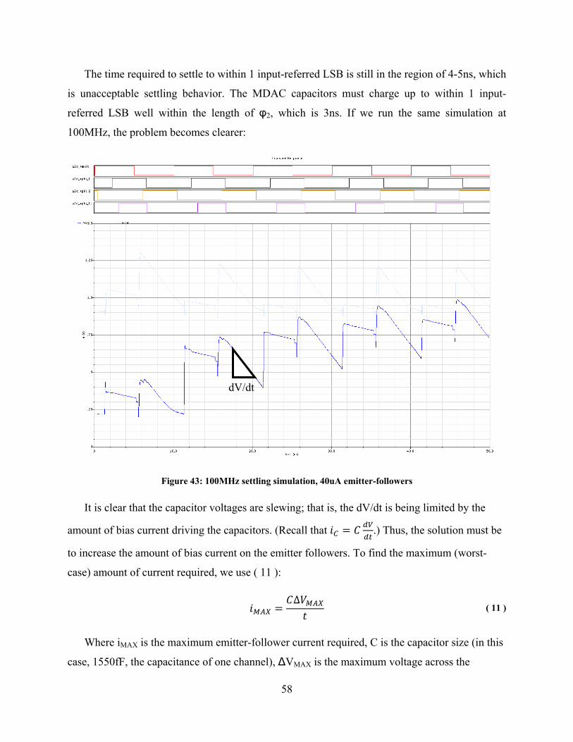
58
The time required to settle to within 1 input-referred LSB is still in the region of 4-5ns, which
is unacceptable settling behavior. The MDAC capacitors must charge up to within 1 input-
referred LSB well within the length of φ2, which is 3ns. If we run the same simulation at
100MHz, the problem becomes clearer:
Figure 43: 100MHz settling simulation, 40uA emitter-followers
It is clear that the capacitor voltages are slewing; that is, the dV/dt is being limited by the
amount of bias current driving the capacitors. (Recall that .) Thus, the solution must be
to increase the amount of bias current on the emitter followers. To find the maximum (worst-
case) amount of current required, we use ( 11 ):
∆
( 11 )
Where iMAX is the maximum emitter-follower current required, C is the capacitor size (in this
case, 1550fF, the capacitance of one channel), ΔVMAX is the maximum voltage across the
dV/dt
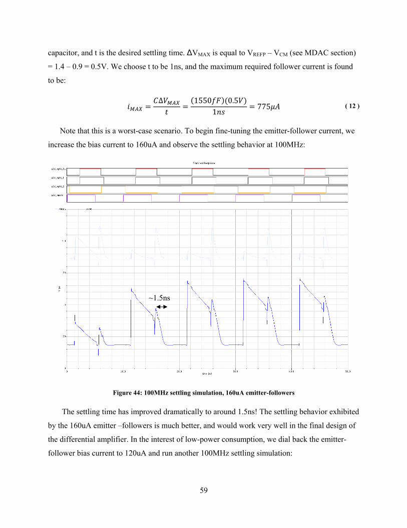
59
capacitor, and t is the desired settling time. ΔVMAX is equal to VREFP – VCM (see MDAC section)
= 1.4 – 0.9 = 0.5V. We choose t to be 1ns, and the maximum required follower current is found
to be:
∆ 1550 0.51 775 ( 12 )
Note that this is a worst-case scenario. To begin fine-tuning the emitter-follower current, we
increase the bias current to 160uA and observe the settling behavior at 100MHz:
Figure 44: 100MHz settling simulation, 160uA emitter-followers
The settling time has improved dramatically to around 1.5ns! The settling behavior exhibited
by the 160uA emitter –followers is much better, and would work very well in the final design of
the differential amplifier. In the interest of low-power consumption, we dial back the emitter-
follower bias current to 120uA and run another 100MHz settling simulation:
~1.5ns

60
Figure 45: 100MHz settling simulation, 120uA emitter-followers
While the settling behavior exhibited in Figure 45 is slightly worse than that of Figure 44
(due to lower emitter-follower bias current), it is still very much acceptable for an output stage
solution in the differential amplifier. Finally, we run one last simulation at 10MHz to ensure that
the output settles adequately to its final value.
~2ns

61
Figure 46: 10MHz settling simulation, 120uA emitter-followers
From Figure 46, we see that the settling within merely 1.3ns of φ2’s falling edge is within 1
input-referred LSB of the final settling value (8.06mV). Thus, we proceed with this design, and
cascade the emitter-follower stages to the outputs of the differential amplifier.
Figure 47: Final emitter-follower design

62
6.1.11 Amplifier Schematic
Figure 48: Differential Amplifier Schematic
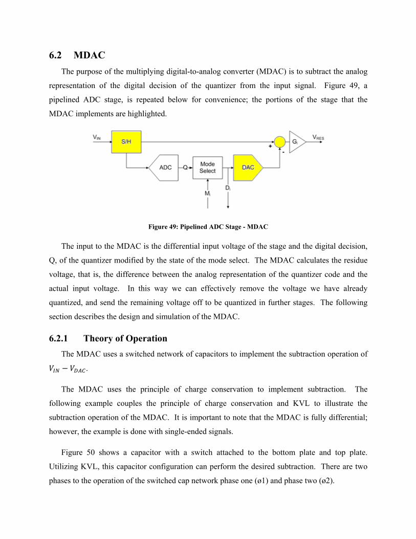
6.2 MDAC The purpose of the multiplying digital-to-analog converter (MDAC) is to subtract the analog
representation of the digital decision of the quantizer from the input signal. Figure 49, a
pipelined ADC stage, is repeated below for convenience; the portions of the stage that the
MDAC implements are highlighted.
Figure 49: Pipelined ADC Stage - MDAC
The input to the MDAC is the differential input voltage of the stage and the digital decision,
Q, of the quantizer modified by the state of the mode select. The MDAC calculates the residue
voltage, that is, the difference between the analog representation of the quantizer code and the
actual input voltage. In this way we can effectively remove the voltage we have already
quantized, and send the remaining voltage off to be quantized in further stages. The following
section describes the design and simulation of the MDAC.
6.2.1 Theory of Operation The MDAC uses a switched network of capacitors to implement the subtraction operation of
.
The MDAC uses the principle of charge conservation to implement subtraction. The
following example couples the principle of charge conservation and KVL to illustrate the
subtraction operation of the MDAC. It is important to note that the MDAC is fully differential;
however, the example is done with single-ended signals.
Figure 50 shows a capacitor with a switch attached to the bottom plate and top plate.
Utilizing KVL, this capacitor configuration can perform the desired subtraction. There are two
phases to the operation of the switched cap network phase one (ø1) and phase two (ø2).

64
Figure 50: MDAC Theory of Operation
Figure 51 shows the capacitor during the first phase, the charge phase. During phase one the
top plate is connected to ground and the bottom plate is connected to a single end of the
differential input signal. The charge on the capacitor is then equivalent to the input voltage times
the value of the capacitance, as seen in the figure below the capacitor.
Figure 51: MDAC Theory of Operation – Phase One
During phase two, as can be seen in Figure 52, the top plate switch is opened in order to
freeze the charge on the capacitor. The bottom plate switch is then connected to VDAC, the
output of the digital decision determined by the quantizer, and the top plate is connected to VOUT.
Figure 52: MDAC Theory of Operation – Phase Two
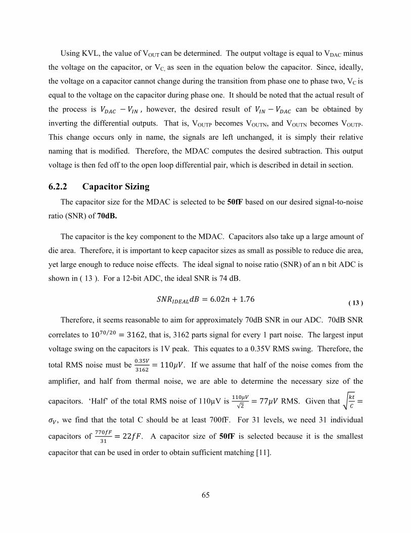
65
Using KVL, the value of VOUT can be determined. The output voltage is equal to VDAC minus
the voltage on the capacitor, or VC, as seen in the equation below the capacitor. Since, ideally,
the voltage on a capacitor cannot change during the transition from phase one to phase two, VC is
equal to the voltage on the capacitor during phase one. It should be noted that the actual result of
the process is , however, the desired result of can be obtained by
inverting the differential outputs. That is, VOUTP becomes VOUTN, and VOUTN becomes VOUTP.
This change occurs only in name, the signals are left unchanged, it is simply their relative
naming that is modified. Therefore, the MDAC computes the desired subtraction. This output
voltage is then fed off to the open loop differential pair, which is described in detail in section.
6.2.2 Capacitor Sizing The capacitor size for the MDAC is selected to be 50fF based on our desired signal-to-noise
ratio (SNR) of 70dB.
The capacitor is the key component to the MDAC. Capacitors also take up a large amount of
die area. Therefore, it is important to keep capacitor sizes as small as possible to reduce die area,
yet large enough to reduce noise effects. The ideal signal to noise ratio (SNR) of an n bit ADC is
shown in ( 13 ). For a 12-bit ADC, the ideal SNR is 74 dB.
6.02 1.76 ( 13 )
Therefore, it seems reasonable to aim for approximately 70dB SNR in our ADC. 70dB SNR
correlates to 10 ⁄ 3162, that is, 3162 parts signal for every 1 part noise. The largest input
voltage swing on the capacitors is 1V peak. This equates to a 0.35V RMS swing. Therefore, the
total RMS noise must be . 110µ . If we assume that half of the noise comes from the
amplifier, and half from thermal noise, we are able to determine the necessary size of the
capacitors. ‘Half’ of the total RMS noise of 110µV is µ√
77µ RMS. Given that
, we find that the total C should be at least 700fF. For 31 levels, we need 31 individual
capacitors of 22 . A capacitor size of 50fF is selected because it is the smallest
capacitor that can be used in order to obtain sufficient matching [11].

66
6.2.3 MDAC Cell Each of the MDACs is comprised of a collection of individual cells. These cells, as can be
seen in Figure 53, are centered around the capacitor, its switches, and the control logic for them.
The logic gates can be seen in block form, and the transistor switches can be seen as transistors.
This block is simply repeated and connected together at the output to simplify design and layout
for stages with different numbers of quantization levels.
Figure 53: MDAC Cell Schematic
Each individual MDAC cell implements the subtraction mechanism outlined in Figure 50,
Figure 51, and Figure 52. The MDAC requires three clocks for its proper operation, which are
generated from the ADC master clock with a series of logic gates.
The three clocks required for operation of the MDAC are designated Φ1, Φ1A, and Φ2. Φ1
and Φ2 correspond to the two major phases of the MDAC operation, charge and evaluate,
respectively. Φ1 and Φ2 are non-overlapping, that is, they are never both simultaneously at a

67
logical high. This allows the connections to the MDAC cell capacitor to “break before make,” so
that no shorting of signals occurs. Specifically, the bottom plate of the capacitor is connected to
the input voltage during Φ1 and the digital decision D during Φ2. It would not be appropriate for
the input voltage to be connected digital decision and the cap simultaneously, as the subtraction
algorithm would not complete successfully.
The clock logic is designed to implement the following logic equations, as seen in Table 5.
The implementation of these equations ensures that the clocks that should not overlap don’t, as
they will not be activated until the other clocks have been de-asserted. In this way we can avoid
having to create the clocks externally, and have to make predictions as to the length of time
required for one clock to transition to another. This method allows for that timing to implement
itself, through the use of the additional logic. It should be noted that Φ2 is creates as per the
equation in Table 5, however, when Φ2 is used to determine other clocks, Φ2 and Φ2 are
actually implemented as Φ2 and Φ2 , the combination of the control signals Φ2P and Φ2M,
as seen in ( 14 ). This method implements the safest implementation with respect to our need for
“break before make” switches.
Φ1A MCLK • Φ2A • Φ2Φ1 Φ2A • Φ2 • Φ1A
Φ2A MCLK • Φ1A • Φ1Φ2 Φ2A • Φ1A • Φ1
Table 5: Clock Generator Logic Equations
Φ2 Φ2M • Φ2P ( 14 )
When determining if it is safe to assert the next clock signal, we must know that the gate
voltages are in the appropriate range to turn the switch transistors off. We cannot be sure of this
condition by sampling the control voltage on up-stream logic gates, due to propagation delays on
the “break” side of the clock. The preceding logic may have transitioned to an off state, but the
following transistors may not have.
However, it is safe to have propagation delays on the “make” side of the clock, because we
can be sure that the previous connections have been broken, if the preceding paragraph has been
implemented correctly, as the switching transistors are known to be off.

68
Figure 54 shows the clocks created by the clock generation block. It can be seen that there is
very little, but non-zero, time at which both Φ1 and Φ2 are low, which is good. It shows that the
“make before break” switching scheme is properly implemented, and also that there is little time
spent not charging or discharging the capacitors; time which could be seen as unproductive, as
more settling time helps with accuracy.
Figure 54: MDAC Clocks
The required logic based on the above analysis is shown in Figure 55.

69
Figure 55: MDAC Clock Generator Logic
6.3 Quantizer The purpose of the quantizer is to convert the input signal from an analog signal to a digital
signal. Figure 56, a pipelined ADC stage, is repeated below for convenience; for our application
the quantizer selected is a flash ADC. Two flash ADCs were designed: one for the first stage
and one for the subsequent stages. The first stage flash ADC has a 65mV step size and 31 levels.
The subsequent stage flash ADC has a 65mV step size and 21 levels. A description of the
selection of those parameters can be found in Section 3.1.
Figure 56: Pipeline ADC Stage: Quantizer

70
The flash ADC is made up of two components: (1) a track and latch comparator and (2) a
preamplifier.
6.3.1 Number of Stages & Number of Bits per Stage The pipelined ADC will contain a total of five stages. Four of the five stages will house a
differential amplifier. The final fifth stage will consist of a quantizer. The first stage of the
pipelined ADC will be characterized by 30 levels (4.9 bits). The four subsequent stages will be
characterized by 21 levels (4.4 bits).
The number of bits per stage can be determined by an analysis of the input and output
voltages, the quantizer step size, and the parameters of the differential amplifier. The input
voltage to the differential amplifier is given by: (VIN – VDAC). The input to the differential
amplifier is called the residue voltage because it is the leftover of the subtraction shown in the
preceding equation. Recall that the input voltage will eventually be converted into (1) n bits and
(2) a residue voltage. The residue voltage is the small amount of voltage that could not be
quantized by the quantizer because it was too small. Specifically, it was smaller than the
quantizer step size q. Therefore, the residue voltage can be expressed as ±q, where q is the
quantizer step size. Mathematically, the quantizer step size q is given by ( 15 ). In ( 15 ), q is the
quantizer step size, 2Vr is the full-scale voltage range of the input voltage to the stage and not to
the differential amplifier (V is half of the full-scale range), and N is the number of quantizer
levels. Refer to Figure 3 and Figure 21 for a visual of the voltage swings through the system.
q2Vr
N ( 15 )
Due to offset errors in the quantizer, a safety margin is incorporated into the value of q. For
more information on quantizer errors, see the design chapter on the quantizer. The residue
voltage will be represented by the value ±q (1+ m), where m is the safety margin. A safety
margin of .5 means that the quantizer step size could be 50% larger or smaller than expected.
An equation for the gain of the differential amplifier can now be derived based on the definitions
derived above. The gain of the differential amplifier can be expressed as the differential output
divided by the differential input. The residue voltage, q(1+ m), is the differential input swing to
the differential amplifier. The differential output swing of the differential amplifier is given in
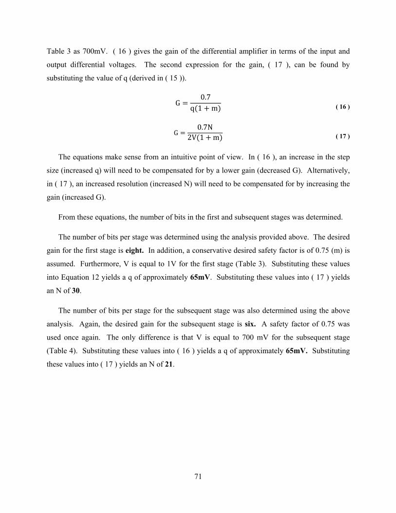
71
Table 3 as 700mV. ( 16 ) gives the gain of the differential amplifier in terms of the input and
output differential voltages. The second expression for the gain, ( 17 ), can be found by
substituting the value of q (derived in ( 15 )).
G0.7
q 1 m ( 16 )
G0.7N
2V 1 m ( 17 )
The equations make sense from an intuitive point of view. In ( 16 ), an increase in the step
size (increased q) will need to be compensated for by a lower gain (decreased G). Alternatively,
in ( 17 ), an increased resolution (increased N) will need to be compensated for by increasing the
gain (increased G).
From these equations, the number of bits in the first and subsequent stages was determined.
The number of bits per stage was determined using the analysis provided above. The desired
gain for the first stage is eight. In addition, a conservative desired safety factor is of 0.75 (m) is
assumed. Furthermore, V is equal to 1V for the first stage (Table 3). Substituting these values
into Equation 12 yields a q of approximately 65mV. Substituting these values into ( 17 ) yields
an N of 30.
The number of bits per stage for the subsequent stage was also determined using the above
analysis. Again, the desired gain for the subsequent stage is six. A safety factor of 0.75 was
used once again. The only difference is that V is equal to 700 mV for the subsequent stage
(Table 4). Substituting these values into ( 16 ) yields a q of approximately 65mV. Substituting
these values into ( 17 ) yields an N of 21.
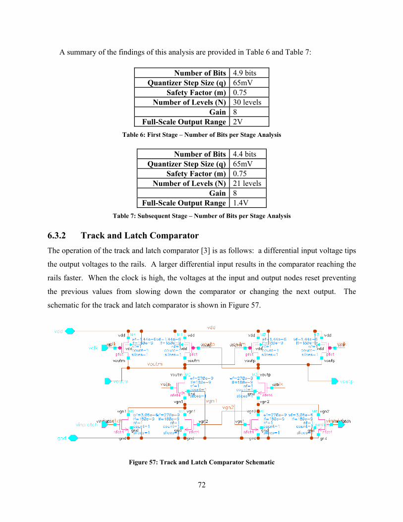
72
A summary of the findings of this analysis are provided in Table 6 and Table 7:
Number of Bits 4.9 bits Quantizer Step Size (q) 65mV
Safety Factor (m) 0.75 Number of Levels (N) 30 levels
Gain 8 Full-Scale Output Range 2V
Table 6: First Stage – Number of Bits per Stage Analysis
Number of Bits 4.4 bits Quantizer Step Size (q) 65mV
Safety Factor (m) 0.75 Number of Levels (N) 21 levels
Gain 8 Full-Scale Output Range 1.4V
Table 7: Subsequent Stage – Number of Bits per Stage Analysis
6.3.2 Track and Latch Comparator The operation of the track and latch comparator [3] is as follows: a differential input voltage tips
the output voltages to the rails. A larger differential input results in the comparator reaching the
rails faster. When the clock is high, the voltages at the input and output nodes reset preventing
the previous values from slowing down the comparator or changing the next output. The
schematic for the track and latch comparator is shown in Figure 57.
Figure 57: Track and Latch Comparator Schematic

73
An important design criterion was the size of the MOSFETs. Natural device mismatch due to
the size of the MOSFETS can be quite large, in the range of 30% of the width according to [1].
A mismatch in M6 and M9 created a large voltage offset; a 20nm change in the width of M6
resulted in a 30mV offset. Using the Cadence simulation tool, the width necessary for a 5mV
offset was determined to be 3μm.
6.3.3 Preamplifier A preamplifier is inserted in front of the latch in order to prevent kickback into the driving
circuitry [3]. Several important considerations must be considered: the effect of the large
threshold range on operation, gain and input capacitance. The schematic for the preamplifier is
shown in Figure 58.
The preamplifier should have a low transconductance in order to reduce the settling time. In
addition, a small amount of input capacitance is required to reduce settling time. The
capacitance values given for the gate oxide capacitance-thin oxide at 1.8V for an NMOS device
is 8.6 fF/um2. As a result, the 21-level quantizer required a width of 3.07μm, retaining the
minimum length and not designing below a capacitor size of 100fF.

74
Figure 58: Preamplifier Schematic
6.3.4 Voltage References The voltage references for the quantizer were established using a resistor ladder and the
supplied 1.8V. 1kΩ resistors were used throughout the ladder in order to partition the supply
voltage into the required references. The resistor size was chosen due to power and size
considerations. Figure 32 and Figure 60 show the configuration of the voltage references for the
quantizers.

75
Figure 59: 31-Level Quantizer Voltage Levels
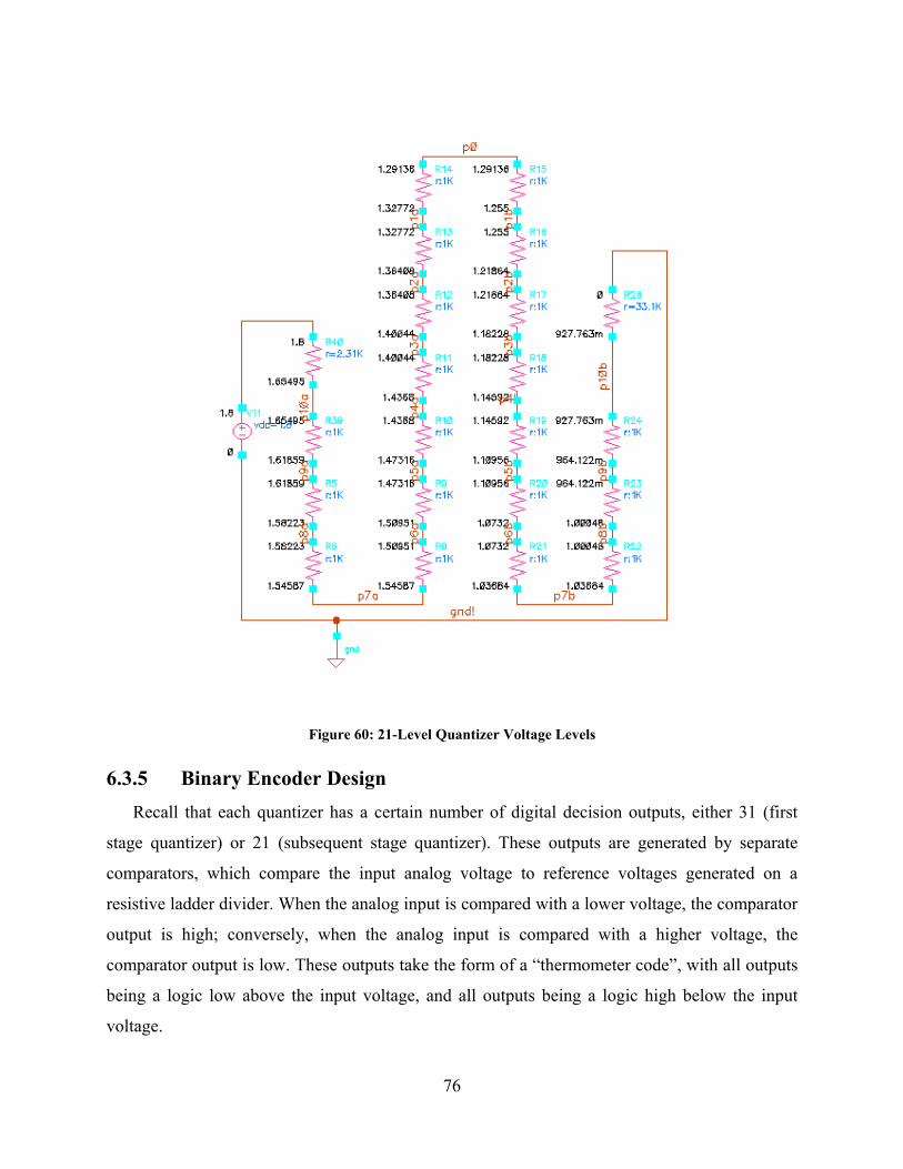
76
Figure 60: 21-Level Quantizer Voltage Levels
6.3.5 Binary Encoder Design Recall that each quantizer has a certain number of digital decision outputs, either 31 (first
stage quantizer) or 21 (subsequent stage quantizer). These outputs are generated by separate
comparators, which compare the input analog voltage to reference voltages generated on a
resistive ladder divider. When the analog input is compared with a lower voltage, the comparator
output is high; conversely, when the analog input is compared with a higher voltage, the
comparator output is low. These outputs take the form of a “thermometer code”, with all outputs
being a logic low above the input voltage, and all outputs being a logic high below the input
voltage.
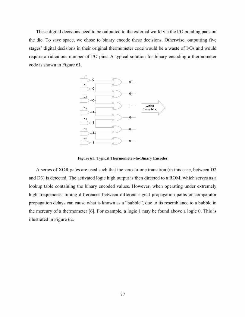
77
These digital decisions need to be outputted to the external world via the I/O bonding pads on
the die. To save space, we chose to binary encode these decisions. Otherwise, outputting five
stages’ digital decisions in their original thermometer code would be a waste of I/Os and would
require a ridiculous number of I/O pins. A typical solution for binary encoding a thermometer
code is shown in Figure 61.
Figure 61: Typical Thermometer-to-Binary Encoder
A series of XOR gates are used such that the zero-to-one transition (in this case, between D2
and D3) is detected. The activated logic high output is then directed to a ROM, which serves as a
lookup table containing the binary encoded values. However, when operating under extremely
high frequencies, timing differences between different signal propagation paths or comparator
propagation delays can cause what is known as a “bubble”, due to its resemblance to a bubble in
the mercury of a thermometer [6]. For example, a logic 1 may be found above a logic 0. This is
illustrated in Figure 62.

78
Figure 62: Thermometer-to-Binary XOR Encoder with a "bubble"
The presence of a bubble will cause an uncertainty in the true zero-to-one transition point
that the XOR gates attempt to find. As a result, two logic lines will be lit up, indicating two
separate addresses to the ROM lookup table, which can cause a catastrophic error in conversion.
A mechanism must be devised to enable the encoder to be tolerant of bubbles.
Mangelsdorf illustrates such a mechanism in [6]. Essentially, this mechanism can be thought
of as a voting process. Each comparator output is compared to the outputs of its adjacent
comparators. If the comparator output differs from both neighbors, that comparator’s output is
toggled. Mangelsdorf gives the following logic equation for this mechanism: For comparators
C1, C2, and C3, the corrected output for comparator C2 is given by C2*:
C2* = C1×C2 + C1×C3 + C2×C3 ( 18 )
This logic function can easily be implemented by a series of AND and OR logic gates.
Applied to the predicament in Figure 62, we see that the problem is fixed in Figure 63.

79
Figure 63: Fixed bubble via correction circuit
[6] further illustrates some fascinating points about this correction scheme. First of all, it
makes no difference how far away a lone comparator output ‘1’ is from the transition point. The
correction scheme will eliminate a lone ‘1’ output no matter where it may lie. Secondly, he
illustrates that either of two patterns, 0011 or 0101, will be recognized as the zero-to-one
transition point in the bank of comparators. Finally, he shows a few cases where the bubble-
correction scheme will work successfully, and where it will fail:
Figure 64: Examples of thermometer-code bubbles
The correction scheme successfully picks the “best guess” transition point in Examples 1, 2,
and 3 of Figure 64. However, in Example 4 of Figure 64, [6] states that the correction scheme
does not fix the bubble. He also notes that the error in Example 4 should only ever occur
between different blocks of comparators, which in our ADC design, should not be a problem.
With regard to this project, each quantizer output and its two neighboring quantizer’s outputs
are fed into a bubble correction block, as shown in Figure 65.

80
Figure 65: Bubble Correction Block
The bubble-correction block effectively implements the logic function in (1). In a logic
diagram, this is represented by Figure 66:
Figure 66: Logic Diagram for Correction Circuit
For the first stage’s quantizer, there will be 31 such blocks. They are connected in a fashion
such that each comparator output goes into three adjacent bubble correction blocks, including its
own. This is shown in Figure 67.

81
Figure 67: Quantizer Bubble-Correction Block (detail)
The output of the bubble-correction block will then represent a “fixed” thermometer code,
which can then be translated into a ROM address for the lookup table containing the binary
encoded quantizer outputs.

82
7 TOP LEVEL CIRCUIT DESIGN The work described in the Top Level Design section includes a preliminary layout of the
design (floor plan) and a description of the pad ring and I/O.
7.1 Floor Plan To begin planning how much die area is needed for the IC, we realize that we would like to
minimize the die area required for our IC in an effort to increase the density of our design per
wafer when the IC is eventually fabricated. There are two main constraints that prevent us from
choosing an infinitesimally small die area: the actual die area that our design requires and the
number of signals that need to be implemented as I/O pins. Each signal going off-chip will need
its own separate bonding pad. In the SBC18HX process, bonding pads are 80µm x 80µm. There
is also a required border around each bonding pad of 12µm. This makes each bonding pad
effectively require 104µm x 104µm of die area:
Figure 68: Bonding pad
Bonding pads must go along the edges of the die area, not including corners. Table 8 shows
a table of all I/O signals that require at least one bonding pad for each half of the split ADC:
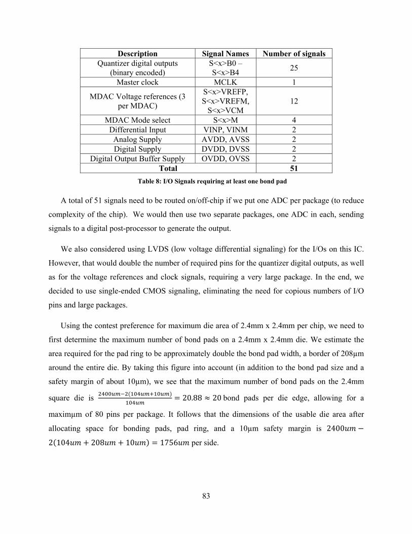
83
Description Signal Names Number of signals Quantizer digital outputs
(binary encoded) S<x>B0 – S<x>B4 25
Master clock MCLK 1
MDAC Voltage references (3 per MDAC)
S<x>VREFP, S<x>VREFM,
S<x>VCM 12
MDAC Mode select S<x>M 4 Differential Input VINP, VINM 2 Analog Supply AVDD, AVSS 2 Digital Supply DVDD, DVSS 2
Digital Output Buffer Supply OVDD, OVSS 2 Total 51
Table 8: I/O Signals requiring at least one bond pad
A total of 51 signals need to be routed on/off-chip if we put one ADC per package (to reduce
complexity of the chip). We would then use two separate packages, one ADC in each, sending
signals to a digital post-processor to generate the output.
We also considered using LVDS (low voltage differential signaling) for the I/Os on this IC.
However, that would double the number of required pins for the quantizer digital outputs, as well
as for the voltage references and clock signals, requiring a very large package. In the end, we
decided to use single-ended CMOS signaling, eliminating the need for copious numbers of I/O
pins and large packages.
Using the contest preference for maximum die area of 2.4mm x 2.4mm per chip, we need to
first determine the maximum number of bond pads on a 2.4mm x 2.4mm die. We estimate the
area required for the pad ring to be approximately double the bond pad width, a border of 208µm
around the entire die. By taking this figure into account (in addition to the bond pad size and a
safety margin of about 10µm), we see that the maximum number of bond pads on the 2.4mm
square die is 20.88 20 bond pads per die edge, allowing for a
maximµm of 80 pins per package. It follows that the dimensions of the usable die area after
allocating space for bonding pads, pad ring, and a 10µm safety margin is 2400
2 104 208 10 1756 per side.

84
Figure 69: 2.4mm square die for ½ split ADC, with bonding pad/pad ring locations
We still need to ensure that the usable die area is large enough to accommodate our IC design
for each ADC. With a 1756µm square usable die area, the total usable die area is 3.083mm2.
The estimated die area requirements for each ADC are summarized below in Table 9:
Functional Block Estimated area required (each) Total area required Quantizer latch (x115) 30µm x 10µm = 300µm2 34,500µm2
Quantizer preamp (x115) 50µm x 10µm = 500µm2 57,500µm2 MDAC cell (x94) 150µm x 10µm = 1,500µm2 141,000µm2
Diff. Amp (x4) 100µm x 310µm = 31,000µm2 124,000µm2
Table 9: Required Die Area (per ADC)
Note: for 4 MDACs, there are three 21-level MDACs and one 31-level MDAC. This is
equivalent to 94 individual MDAC cells.

85
Five quantizers are required: four 21-level quantizers and one 31-level quantizer. Each
quantizer level requires one latch and one preamplifier, requiring a total of 115 latches and
preamps.
From Table 9, we see that the estimated total die area required for one ADC is 357,000µm2.
Even if we double the estimated total die area as a safety measure to 714,000µm2, we are still
well within the total usable die area of 3.083mm2 from the I/O pin constraint.
Also as Table 9 shows, a preliminary layout of the quantizer, MDAC, and differential
amplifier allows us to estimate how much die area will be required for one ADC. With those
numbers, we chose to begin layout of the ADC around a single MDAC cell, which can be laid
out to be approximately 150µm x 10µm. With one quantizer preamplifier and latch per MDAC
cell, we chose to put each MDAC cell adjacent to its corresponding quantizer preamp and latch.
Figure 70 shows a quantizer preamplifier and latch (resized to fit into a 30µm square) placed
adjacent to an MDAC cell:
Figure 70: Quantizer and MDAC cell
There will be 31 such cells for the first pipeline stage. When stacked vertically, the result is
a rectangular die area 80µm wide and 930µm tall. The differential amplifier then follows the
MDAC. For subsequent pipeline stages, there will only be 21 quantizer and MDAC cells. Both
versions are shown in Figure 71.

86
Figure 71: Pipeline Stage Floorplan
Note that there will need to be two separate layouts of the differential amplifier to minimize
unused area on the die. One layout will be approximately 310µm x 100µm, for use in the first
stage, while all subsequent amplifiers’ layout will be approximately 210µm x 150µm.
Using this information, we can layout each ADC in stages, as shown in Figure 72:
Figure 72: ADC Stage Layout
Each ADC will require about 1600µm x 310µm of die area for a stage-sequential layout as
shown in Figure 72. Figure 73 shows a potential layout of a single ADC on the die.

87
Figure 73: 80-pad Die with 1 ADC (1/2 split)

88
Figure 74 shows a diagram of the 80-pad die with potential signals for each of the pads. The
signals have been placed for optimal signal routing. Groups of signals for a particular stage have
had their pads highlighted in different colors. All stages share the same voltage supplies and
clock signals, provided on the left edge of the die.
1. NC2. NC3. NC
4. OVDD5. OVSS
6. NC7. AVDD8. AVSS
9. NC10. VINP11. VINM
12. NC13. DVDD14. DVSS
15. NC16. MCLK
17. ~MCLK18. NC19. NC20. NC
21. N
C22
. S1B
023
. S1B
124
. S1B
225
. S1B
326
. S1B
427
. S1M
28. S
1VR
EFP
29. S
1VR
EFM
30. S
1MV
CM
31. S
1AV
CM
32. N
C33
. S3B
034
. S3B
135
. S3B
236
. S3B
337
. S3B
438
. S3M
39. S
3VR
EFP
40. S
3VR
EFM
51. S5B250. S5B349. S5B448. NC47. NC46. NC45. NC44. NC43. NC42. S3AVCM41. S3MVCM
80. N
C79
. S2B
078
. S2B
177
. S2B
276
. S2B
375
. S2B
474
. S2M
73. S
2VR
EFP
72. S
2VR
EFM
71. S
2MVC
M70
. S2A
VCM
69. N
C68
. S4B
067
. S4B
166
. S4B
265
. S4B
364
. S4B
463
. S4M
62. S
4VR
EFP
61. S
4VR
EFM
52. S2B153. S5B054. NC55. NC56. NC57. NC58. NC59. S4AVCM60. S4MVCM
Figure 74: Potential Pin Layout and Floor Plan for 80-Pad Die

89
However, it seems that there is an excessive amount of unutilized die area, as well as a large
number of unconnected pads on the die. We therefore seek to reduce the die size further by
shrinking down the top and bottom edges of the die, and removing excessive unconnected pads.
We also isolate the high-speed digital stage outputs to one side of the die, and move all of the
analog pads to the other side, to separate analog and digital power domains, as well as to ease
routing of signals on the die. Additionally, we double up on the number of all supply pads. The
result is seen in Figure 75.
1. AVDD2. AVSS
3. NC4. NC
5. VINP6. VINM
7. NC8. NC
9. AVSS10. AVDD
40. S3B339. S3B438. S5B037. S5B136. S5B235. S5B334. S5B433. S4B032. S4B131. S4B2
11. S
2VR
EFP
12. S
2VR
EFM
13. S
2VC
M14
. S4V
RE
FP15
. S4V
RE
FM16
. S
4VC
M17
. MC
LK18
. DV
DD
19. D
VS
S20
. S2M
21. S
2B4
22. S
2B3
23. S
2B2
24. S
2B1
25. S
2B0
26. S
4M27
. S4B
428
. S4B
329
. OV
DD
30. O
VS
S
60. S
1VR
EFP
59. S
1VR
EFM
58.
S1V
CM
57. S
3VR
EFP
56. S
3VR
EFM
55. S
3VC
M54
. DV
DD
53. D
VS
S52
. S1M
51. S
1B0
50. S
1B1
49. S
1B2
48. S
1B3
47. S
1B4
46. S
3M45
. S3B
044
. S3B
143
. S3B
242
. OV
DD
41. O
VS
S
624um
2400um
1756um
1268um
Figure 75: Potential Pin Layout and Floor Plan for 60-Pad Die
The die is now considerably smaller at 2400µm x 1268µm, about half the size of the die
shown in Figure 74. The high-speed digital output pads are located on the right side of the die
and are highlighted in red, while the analog circuitry is to the left and highlighted in blue. In the
middle are the digital supplies to each stage’s quantizer and MDAC, as well as the mode select
input pads to each stage. These are highlighted in green.
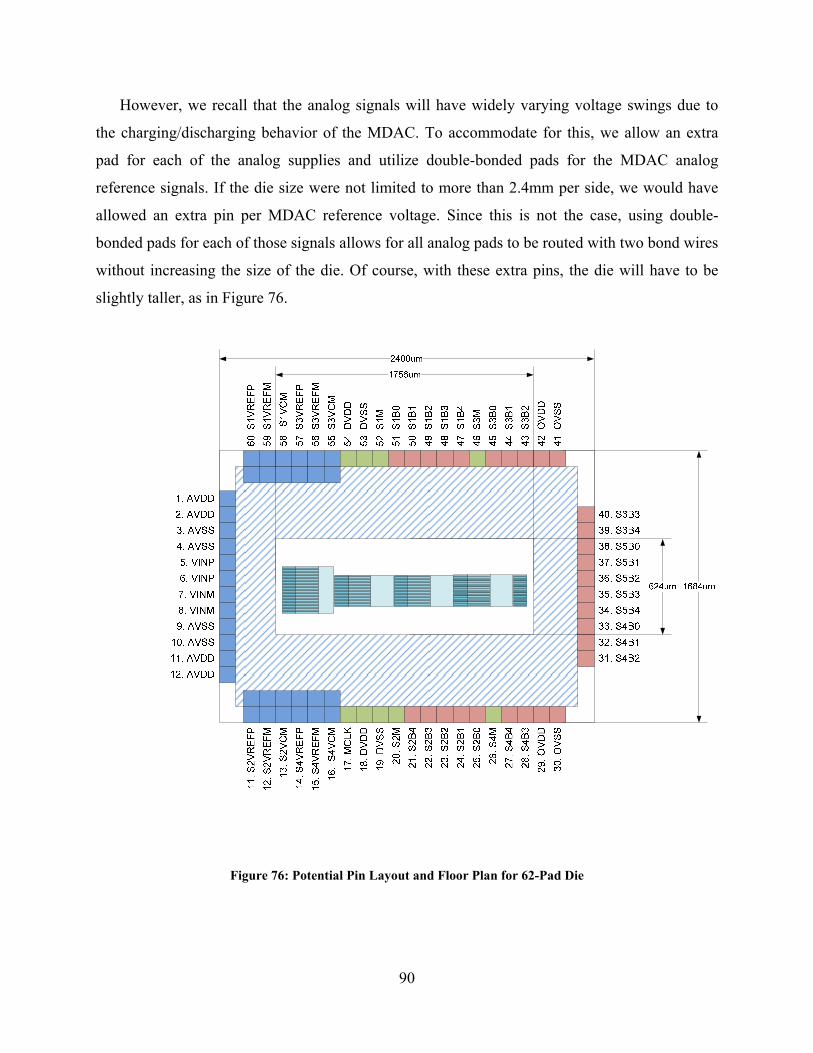
90
However, we recall that the analog signals will have widely varying voltage swings due to
the charging/discharging behavior of the MDAC. To accommodate for this, we allow an extra
pad for each of the analog supplies and utilize double-bonded pads for the MDAC analog
reference signals. If the die size were not limited to more than 2.4mm per side, we would have
allowed an extra pin per MDAC reference voltage. Since this is not the case, using double-
bonded pads for each of those signals allows for all analog pads to be routed with two bond wires
without increasing the size of the die. Of course, with these extra pins, the die will have to be
slightly taller, as in Figure 76.
Figure 76: Potential Pin Layout and Floor Plan for 62-Pad Die

91
The die is now slightly larger at 2400µm x 1684µm, and there are now 62 pads on the die.
Analog signals on the left edge have been given an additional bonding pad, while MDAC
reference voltages on the top and bottom edges have double-bonded pads.
Figure 76 represents a feasible floor plan of the die, and is the final revision of our floor plan
7.2 Pad Ring The pad ring for the ADC consists of ESD-protection circuitry. This includes ESD protection
diodes for each I/O to both voltage supply rails (VDD and VSS) as well as voltage-limiting
power supply clamp cells. The following figure from [9] illustrates the proper use of ESD diodes
and power supply clamp cells in a custom mixed-signal integrated circuit:
Figure 77: Proper Implementation of ESD Devices in custom Mixed-Signal IC
There are two ESD diodes allocated per bond pad, allowing a path through which excess
current can travel when two or more bond pads are subjected to ESD. Additionally, there are
large NPN power supply clamp cells regulating voltage supply rails (i.e. VDD and VSS). These
ESD protection devices will be located next to the bonding pads on our IC, in a structure known
as a pad ring, for which we have allocated a 50µm wide strip encircling the entire die. In
schematic form, the pad ring consists of an “ESD cell” for each I/O pad ring, whose schematic is
shown in Figure 78:

92
Figure 78: ESD cell
The ESD cell consists of two ESD diodes, one going from the pad to the positive voltage
supply rail, and one going to ground. This ensures an ESD discharge path to either VDD or VSS.
The actual pad ring implementation includes one of these ESD cells per I/O, in addition to a set
of cross-coupled ESD diodes separating voltage supply grounds and a power supply clamp cell
per set of voltage rails. These are shown in Figure 79 and Figure 80.
Figure 79: Cross-coupled ESD diodes and power supply clamp cells
Figure 80: Some ESD cells in the pad ring

93
8 VERIFICATION The work described in the Verification section includes simulated performance data results of
the open-loop residue amplifier, MDAC, and quantizer in addition to system level performance
results. Also, the section includes a plan to verify the final layout in Phase Two and a plan to
evaluate and test the final fabricated design.
8.1 Open-Loop Residue Amplifier There are certain criteria that the open-loop differential amplifier must meet or exceed:
sufficient differential gain and ample differential output voltage swing.
8.1.1 Differential Gain and Output Swing To verify the first two criteria of differential gain and differential output swing, we can
perform a DC sweep and plot the differential input-output characteristic. Note that the addition
of the BJT emitter-follower stage drops the output common-mode of the differential amplifier to
580mV. This is not a problem for the next stage, explained earlier in Section 6.1.10, Output
Stage Design.
Figure 81: DC sweep of Differential Amplifier
Figure 81 shows the DC sweep of the differential amplifier. Both outputs of the differential
amplifier are plotted vs. differential input voltage. Taking the two points M2 and M3 in Figure
81, we see that the slope of the transfer function for a single output is approximately -4.02. To

94
find the differential gain of the entire amplifier, we double this number, giving us a differential
gain of 8.04, very close to the gain of 8 that we designed for.
Figure 81 also shows the output range of the differential amplifier in terms of the edges of its
roughly-linear range. The output range is seen to be around 692mV, very close to the 700mV
output swing we designed for.
8.1.2 Power Consumption In terms of power consumption, we can add up the bias current required for each part of the
differential amplifier. This includes the main differential pair, replica biasing, common-mode
feedback differential pair, common-mode feedback helper current, current mirroring (current-
setting devices and N-to-P devices), and resistive dividers. This is shown in Table 10. The
numbers derived in Table 10 come from examining an annotated schematic of the DC bias rail
and resistive dividers, as shown in Figure 82.
Current Consumption Main mirror 200uA CMFB Differential Pair 84uA N-to-P mirrors 600uA Replica Bias 225uA CMFB Helper Currents 1520uA Output Stage (Emitter Follower) 240uA Main Differential Pair 1977uA
Resistive Dividers 134uA 128uA 86uA
Total 5194uA Table 10: Current consumption

95
Figure 82: DC Bias Rail and Resistive Dividers
The differential pair draws a total of 5.194mA, at a supply voltage of VDD = 1.8V. This is a
total of 9.3mW. Using the formula for figure-of-merit in ( 19 ),
( )( )2
/sumberofBitEffectiveN
SpeedmptionPowerConsu=FOM ( 19 )
and assuming that the differential amplifier dominates power consumption in the overall ADC,
as well as assuming that differential amplifiers in the 3 subsequent stages can be scaled down
such that all 3 amplifiers consume a total current equivalent to that consumed by the first stage
amplifier, we see that the figure of merit for our ADC design is roughly 1.29pJ/step, running a
12-bit ADC at 100MHz. This is relatively close to the industry ‘standard’ of about 1pJ/step in
efficiency of conversion.
Our target figure of merit for this ADC was 0.5pJ/step. If we re-use the assumptions stated
in the previous paragraph, it is possible to tweak the differential amplifier to produce an ADC

96
with an overall figure of merit of approximately 0.75pJ/step. This would involve lowering the
power consumption of the differential amplifier and also decreasing the differential gain of the
amplifier. If the gain is lowered to 6, it is estimated that power consumption of the differential
amplifier could be reduced by 40%, to a total of 11.2mW for four amplifiers. Also, since we
have five 5-bit stages, producing a raw 25-bit output (before overlap, digital post-processing,
etc.), it is conceivable that a 14-bit result could be produced rather than a 12-bit result. If these
modifications were made, it would be possible to obtain a 14-bit ADC operating at 100MHz with
a figure of merit of 0.571pJ/step.
8.1.3 Overall Amplifier Specification From the design of the quantizer, we know that the differential input to the differential
amplifier should not exceed 65mV, the quantizer step size. However, we have increased this
margin to 87.5mV due to the gain of 8.
The specification table for the amplifier is thus as follows:
Input Voltage 900mV ± 87.5mV Differential Input Swing ± 175mV Output Voltage 580mV ± 350mV Differential Output Swing ± 700mV Differential Gain 8.04 Voltage Supply +1.8V Current 5.0331mA Power Dissipation 9.05mW Power FOM 1.25pJ/step Input Resistance ∞ Output Resistance 800Ω
Table 11: Differential Amplifier Specification
This specification meets and/or exceeds our design evaluation criteria.
8.2 MDAC As a standalone block, the most important function that the MDAC implement is the
subtraction algorithm. As such, the following shows the process used to verify the proper
functionality of the implementation of that algorithm, as described in previous sections. Figure
83 shows a portion of a MDAC verification simulation. In this simulation, a 15-level MDAC is

97
tested. In this test, the input differential voltage was swept, while the digital decisions were
incremented correspondingly. This will help to show that the subtraction takes properly, and will
help to assess the accuracy of the subtraction. A summary of the values shown in Figure 83 are
displayed in Table 12. Shown are the differential input voltages, Vinn and Vinp. Additionally,
the output voltages created by the simulation and the ideal calculated output values are shown.
Finally, an error is calculated by examining the difference between the ideal calculated
differential output voltage and the simulated differential output.
Vinn Voutp Sim Voutp Calc535.00 862.00 898.33547.00 859.00 886.33559.00 847.00 874.33572.00 836.00 861.33584.00 824.00 849.33
Vinp Voutn Sim Voutn Calc
1265.00 871.00 901.671253.00 874.00 913.671240.00 886.00 926.671227.00 898.00 939.671215.00 910.00 951.67
Vind Voutd Sim Voutd Calc Error
730.00 9.00 3.33 5.67706.00 15.00 27.33 -12.33681.00 39.00 52.33 -13.33655.00 62.00 78.33 -16.33631.00 86.00 102.33 -16.33
Table 12: MDAC Verification Simulation Summary (all voltages in mV)
As can be seen, the errors stay in the range of 15mV. Given a 15-level quantizer and a 1V
FSR, the 15mV error is well within ½ of an LSB, that being 33mV. This shows with reasonable
certainty that the MDAC operates properly, at the required frequency.

98
Figure 83: MDAC Verification Simulation

99
8.3 Quantizer Figure 84 verifies the behavior of one decision level of a 21-level quantizer. The levels are
numbered n15 (-15) to +15 including 0. Each of the colored lines (quantizer levels) represents
the negative differential output subtracted from the positive differential output. The output
combination shown in Figure 84 represents an input differential voltage of 950mV, a value in
between the threshold for latches +14 and +15. The +15 latch settles at the negative rail because
950mV is lower than the threshold for latch +15. The input voltage of 950mV is higher than the
threshold for all latches below +15; as a result, these latches all settle at the positive rail.
Figure 84: 21-Level Single-Decision Quantizer Verification Simulation
A 31-level quantizer was also constructed, tested, and completely verified. The full-scale
input of the quantizer was swept and the digital decisions were plotted. The full data table and
plot of the outputs can be found in APPENDIX F: 31-Level Quantizer Verification.

100
8.4 Phase Two Hardware Plan We have outlined the path we will take to (1) to verify the final layout and (2) evaluate and
test the final fabricated design.
Between the March 15th announcement of the winners of Phase One and the May 15th
deadline for Phase Two Initial Submissions, the layout of the IC will be completed and will pass
all LVS and DRC requirements. A proposed schedule for the completion of the project is shown
below.
The chip will be tested and evaluated using an FPGA coupled with the digital correction
algorithm described in [9].
Figure 85: Schedule of Layout Completion
A picture of the eventual evaluation of the IC with the FPGA, PC, and data collection is
shown in Figure 86.

101
Figure 86: ADC IC with FPGA, PC, and Data Collection
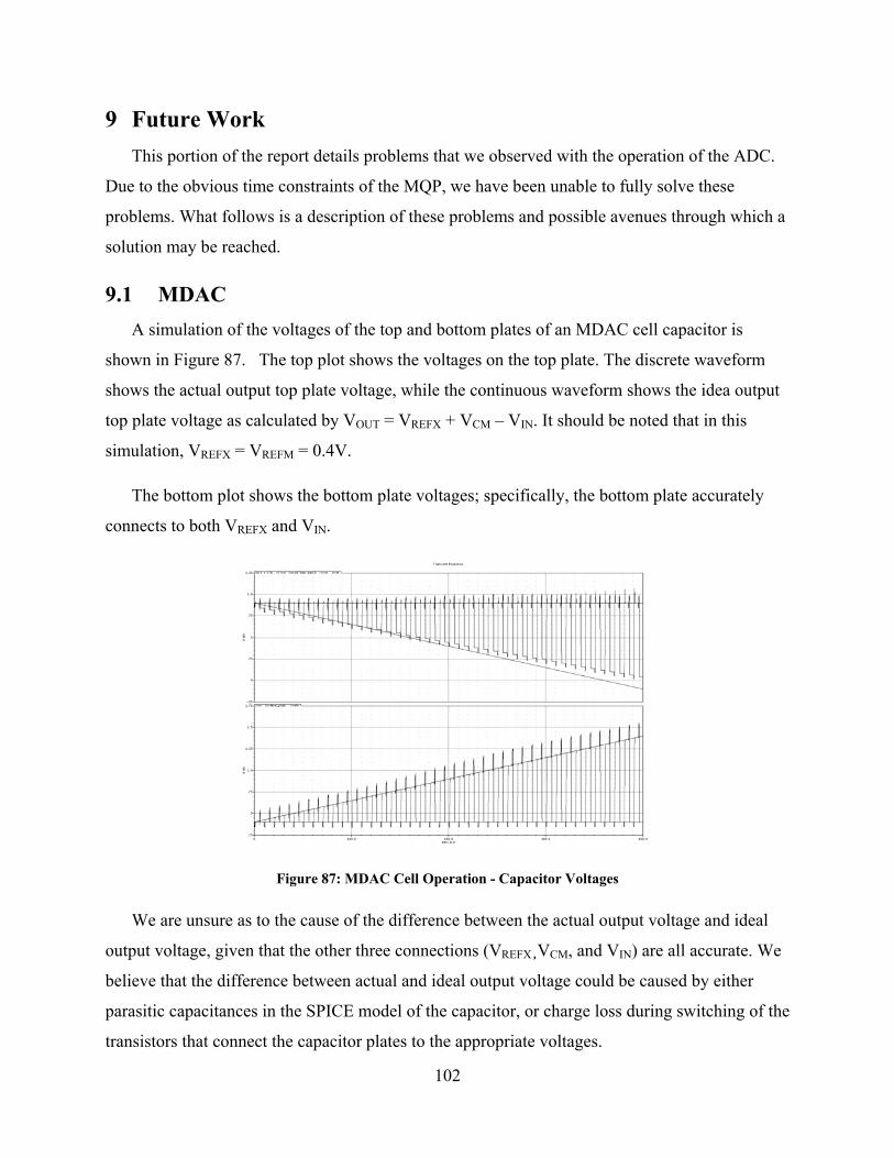
102
9 Future Work This portion of the report details problems that we observed with the operation of the ADC.
Due to the obvious time constraints of the MQP, we have been unable to fully solve these
problems. What follows is a description of these problems and possible avenues through which a
solution may be reached.
9.1 MDAC A simulation of the voltages of the top and bottom plates of an MDAC cell capacitor is
shown in Figure 87. The top plot shows the voltages on the top plate. The discrete waveform
shows the actual output top plate voltage, while the continuous waveform shows the idea output
top plate voltage as calculated by VOUT = VREFX + VCM – VIN. It should be noted that in this
simulation, VREFX = VREFM = 0.4V.
The bottom plot shows the bottom plate voltages; specifically, the bottom plate accurately
connects to both VREFX and VIN.
Figure 87: MDAC Cell Operation - Capacitor Voltages
We are unsure as to the cause of the difference between the actual output voltage and ideal
output voltage, given that the other three connections (VREFX¸VCM, and VIN) are all accurate. We
believe that the difference between actual and ideal output voltage could be caused by either
parasitic capacitances in the SPICE model of the capacitor, or charge loss during switching of the
transistors that connect the capacitor plates to the appropriate voltages.
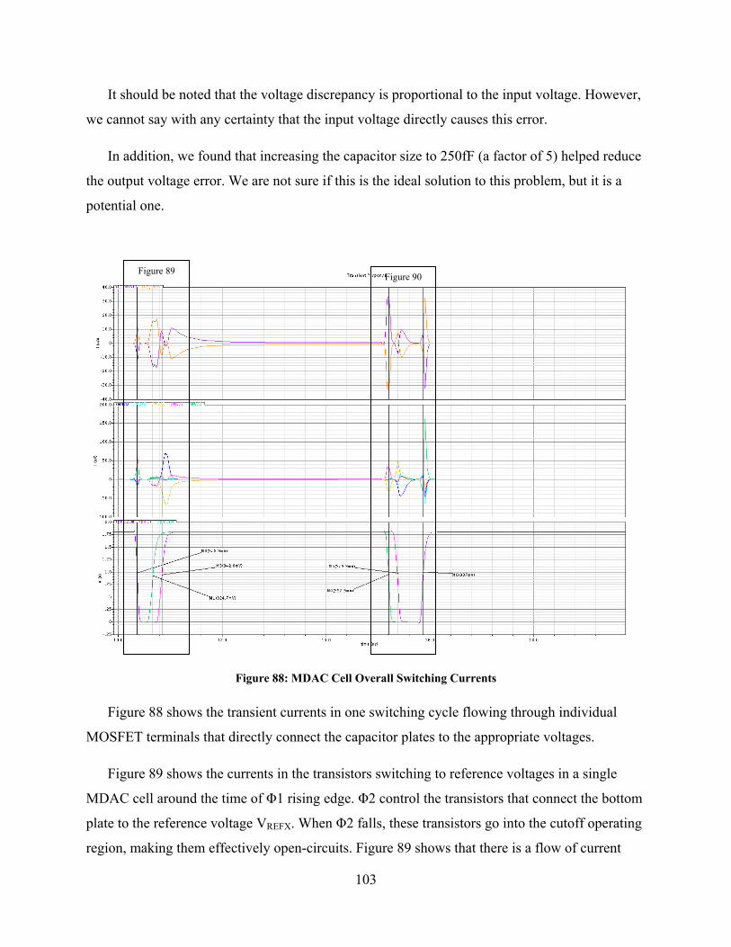
103
It should be noted that the voltage discrepancy is proportional to the input voltage. However,
we cannot say with any certainty that the input voltage directly causes this error.
In addition, we found that increasing the capacitor size to 250fF (a factor of 5) helped reduce
the output voltage error. We are not sure if this is the ideal solution to this problem, but it is a
potential one.
Figure 88: MDAC Cell Overall Switching Currents
Figure 88 shows the transient currents in one switching cycle flowing through individual
MOSFET terminals that directly connect the capacitor plates to the appropriate voltages.
Figure 89 shows the currents in the transistors switching to reference voltages in a single
MDAC cell around the time of Φ1 rising edge. Φ2 control the transistors that connect the bottom
plate to the reference voltage VREFX. When Φ2 falls, these transistors go into the cutoff operating
region, making them effectively open-circuits. Figure 89 shows that there is a flow of current
Figure 89 Figure 90

104
through these (and other) transistors. We are unsure as to why this happens; it is our belief that
when a transistor “turns off”, there should be no flow of charge.
Additionally, when Φ1A and Φ1 rise in Figure 89, current flows through transistors that are
in the cutoff region. The transistors that should be in cutoff are the ones that connect the bottom
plate to VREFX. Again, we are unsure as to why this happens, but we think that this flow of charge
could potentially be causing discrepancies in the subtraction.
Figure 89: Currents during Φ2 falling edge, Φ1A/Φ1 rising edges
Figure 90 shows similar behavior during the falling edges of Φ1A/Φ1 and the rising edge of
Φ2. During this phase, the transistors that should be in cutoff are the analog transmission gate to
VIN and the NMOS switch to VCM. However, there is current flowing through these transistors.
Again, we think that this stray current is the charge loss that is causing the voltage
discrepancies seen in Figure 87.

105
Figure 90: Currents during Φ1A/Φ1 falling edges, Φ2 rising edge
9.2 Differential Amplifier The open-loop differential amplifier is a key component to the appeal of our overall ADC.
Murmann [10] showed that the power savings in using an open-loop amplifier stage as opposed
to a traditional closed-loop amplifier stage in a pipelined ADC was around 60%. Although the
use of an open-loop amplifier has driven the speed-power figure of merit of our ADC to around
0.571pJ/step, there are certainly several optimizations to the differential amplifier that could be
implemented. However, due to the obvious time constraints of the MQP, this analysis and
optimization was overlooked in favor of coarse functionality of the overall ADC.
The most important specification of the differential amplifier (from a system-level point of
view) was that it be a low-power solution. It follows that the power draw of the differential
amplifier should be optimized, given that it dominates the power dissipation of the entire ADC.
However, for a fixed resolution pipelined ADC, there is probably a tradeoff between the
attainable differential gain and the overall number of stages required to reach that resolution. In

106
other words, the differential gain required was determined by the number of quantization levels
chosen per stage. Conversely, the number of quantization levels could be determined by the
attainable differential gain.
Our design philosophy was to simply choose some design parameters and, based on those
decisions, determine the other required parameters. This was done to simplify and hasten the
design process. In future work, some analysis could be done to determine a more optimum
solution in terms of overall power consumption for a fixed resolution ADC.

107
10 CONCLUSION The completed 12b 100MSps pipeline ADC design represents application of the novel “Split
ADC” concept to drastically reduce power consumption and improve performance as measured
by the pJ/step FOM for ADCs in the important application area of portable ultrasound. Rather
than push absolute limits, we have chosen a target in an important application space with
moderate speed and resolution; the high performance aspect of the design will be the
improvement in the speed-power FOM. For a representative ADC such as the ADS5270 [13],
the FOM is approximately 1 pJ/step; in addition, the power dissipation in one ADC is 113mW.
Through the use of an open-loop residue amplifier we achieved sufficient power savings to
improve the FOM to 0.571pJ/step and the power dissipation in one ADC to 11.2mW.

108
11 REFERENCES [1] D. Boning and S. Nassif, “Models of Process Variations in Device and Interconnect, in
Design of High-Performance Microprocessor Circuits,” 2000.
[2] “How ADC Errors Affect System Performance.”
http://pdfserv.maximic.com/en/an/AN748.pdf. 5 October 2008.
[3] D. Johns and K. Martin, “Analog Integrated Circuit Design,” John Wiley & Sons, Inc.,
1997.
[4] A. N. Karanicolas, H. Lee, and K. Bacrania, “A 15-b 1-Msample/s Digitally Self-Calibrated
Pipeline ADC.” IEEE J. Solid-State Circuits, Vol. 28, No. 12, Dec. 1993.
[5] J. Li and U. Moon, “Background calibration techniques for multi-stage pipeline ADCs with
digital redundancy,” IEEE Trans. Circuits Syst. II, pp. 531-538, Sep. 2003.
[6] C. Mangelsdorf, “A 400-MHz Input Flash Converter with Error Correction,” IEEE J. Solid-
State Circuits, Vol. 25, No. 1, Feb. 1990.
[7] J. McNeill. Analog-to-Digital Converter Block Diagram. ECE 3204, Lecture notes.
[8] J. McNeill, M. Coln, and B. Larivee, “‘Split-ADC’ Architecture for Deterministic Digital
Background Calibration of a 16b 1MS/s ADC,” IEEE J. Solid-State Circuits, pp. 2437-2445,
Dec. 2005.
[9] J. McNeill, S. Goluguri, and A. Nair, “‘Split-ADC’ Digital Background Correction of Open-
Loop Residue Amplifier Nonlinearity Errors in a 14b Pipeline ADC,” Proc. ISCAS2007,
May, 2007.
[10] B. Murmann and B.E. Boser, “A 12b 75MS/s Pipeline ADC using Open-Loop Residue
Amplification,” IEEE J. Solid-State Circuits, pp. 2040-2050, Dec. 2003.
[11] M. Pelgrom, A. Duinmaijer, and A. Welbers, “Matching Properties of MOS Transistors,”
IEEE J. Solid-State Circuits, pp. 1433-1440, Oct. 1989.
[12] D. Quon, “Jazz Semiconductor ESD Design Manual.” Document NPB PS-0411, August
2004.
[13] ADS5270 Data Sheet, Texas Instruments.

109
APPENDIX A: MATLAB Uncorrelated ADC Simulator The below code simulates a 12-bit 5-stage uncorrected pipelined ADC resolving 3 bits per stage (except the
last stage, resolving 4 bits) utilizing an open-loop differential pair residue amplifier in the first stage. The
simulator also implements a mode select feature which effectively shifts the digital output by ± ½ LSB.
Additionally, the simulated pipeline ADC operates on supply voltage rails of ±2.5V. The simulator takes an
input of an input vector. To obtain residue and decision plots, the input vector can be set as a sweep of the input
voltage. The resulting digital decisions from each stage are saved in variables s1d – s5d and the analog residues
saved into variables s1r – s5r. The digital decisions from each stage are reconverted to analog voltages and
output as the variable ‘result’.
function[result] = adcSim(inputVector,mode) m = 0; if mode m = 0.5; else m = -0.5; end gain = 4; bitsPerStage = 3; bitsFinalADC = 4; adcLowFSR = -2.5; adcHighFSR = 2.5; adcFSR = adcHighFSR - adcLowFSR; Vstep = adcFSR/(2^bitsPerStage); VstepFinalADC = adcFSR/(2^bitsFinalADC); s1d = []; % stage 1 decisions s1r = []; % stage 1 residues s2d = []; s2r = []; s3d = []; s3r = []; s4d = []; s4r = []; s5d = []; Vin = inputVector; % stage 1 s1d = (sign(Vin).*(Vstep*round(abs(Vin)/Vstep))); s1d = s1d + m; s1r = Vin-(sign(Vin).*(Vstep*round(abs(Vin)/Vstep))); s1r = diffPairNonLin(s1r,gain); %s1r = s1r.*gain; % stage 2 s2d = (sign(s1r).*(Vstep*round(abs(s1r)/Vstep))); s2d = s2d + m;

110
s2r = s1r-(sign(s1r).*(Vstep*round(abs(s1r)/Vstep))); s2r = s2r.*gain; % stage 3 s3d = (sign(s2r).*(Vstep*round(abs(s2r)/Vstep))); s3d = s3d + m; s3r = s2r-(sign(s2r).*(Vstep*round(abs(s2r)/Vstep))); s3r = s3r.*gain; % stage 4 s4d = (sign(s3r).*(Vstep*round(abs(s3r)/Vstep))); s4d = s4d + m; s4r = s3r-(sign(s3r).*(Vstep*round(abs(s3r)/Vstep))); s4r = s4r.*gain; % stage 5 s5d = (sign(s4r).*(VstepFinalADC*round(abs(s4r)/VstepFinalADC))); result = s1d + s2d + s3d + s4d + s5d;
The function diffPairNonLin controls the nonlinearity of the differential pair gain. The differential pair
nonlinearity is modeled upon a constant gain (first order term) as well as a cubic nonlinearity term dependent on
a nonlinearity coefficient α and a MOSFET overdrive voltage VOV. The code for this function is displayed
below:
function Vod = diffPairNonLin(Vid,G) % nonlinearity in diff pair alpha = 0.133/32; Vov = 0.25; Vod = G.*Vid - alpha*G/(Vov^2).*Vid.^3;

111
APPENDIX B: INL/DNL Calculator The following code will import a dataset as saved in an n-by-1 sized array of digital codes produced from a
linear sweep of input voltage and derive from them the corresponding differential and integral nonlinearity in
two ways.
Differential nonlinearity is calculated as the ratio of actual hits divided by ideal hits, minus 1. The number if
ideal hits per code transition should be the total number of digital decisions divided by 2N, where N is the total
number of bits, if the input to the ADC is linear.
The first method if INL calculation is simply the cumulative sum of the DNL. The second method of INL
calculation is by deviation from ideal transfer function. The slope of the actual data is calculated via the
MATLAB function ‘regress’. Knowing this, the slope of the actual data can be corrected. From this gain
corrected data the INL can be calculated, given that the input is swept linearly and with an input that is
monotonically increasing.
%number of bits in adc nbits = 12; %load data set load('\\ … datafile.mat') %rotate output = output'; %collect histogram data from input dataset [counts, bins]=hist(output, min(output):1:max(output)); %ideal 'hits' per code transition based on linear input datapointsperct = length(output)/2^nbits; %calculate dnl dnl = (counts./datapointsperct)-1; %calculate inl as sum of dnl inl1 = cumsum(dnl); mainlsum = max(inl1); %calculate inl as deviation from gain corrected ideal b = regress(output', Vin'); gaincorrectedoutput = output./b.*(2^nbits/5); x = min(Vin):max(Vin)/max(bins):max(Vin); inl2 = Vin./5.*2^12 - gaincorrectedoutput; maxinlcalc = max(inl2); %plot results subplot(3, 1, 1), plot(bins, dnl), title('Differential Nonlinearity'), , xlabel('Digital Code'), ylabel('DNL [LSB]'), grid; v = axis; axis([v(1) 2^nbits v(3) v(4)]) subplot(3, 1, 2), plot(bins, inl1), title('Integral Nonlinearaity as sum of DNL'), xlabel('Digital Code'), ylabel('INL [LSB]'), grid; v = axis; axis([v(1) 2^nbits v(3) v(4)]) subplot(3, 1, 3), plot(Vin.*2^12./5, inl2), title('Integral Nonlinearaity as Calculated from Ideal'), xlabel('V_In'), ylabel('INL [LSB]'), grid; v = axis; axis([v(1) 2^nbits v(3) v(4)])
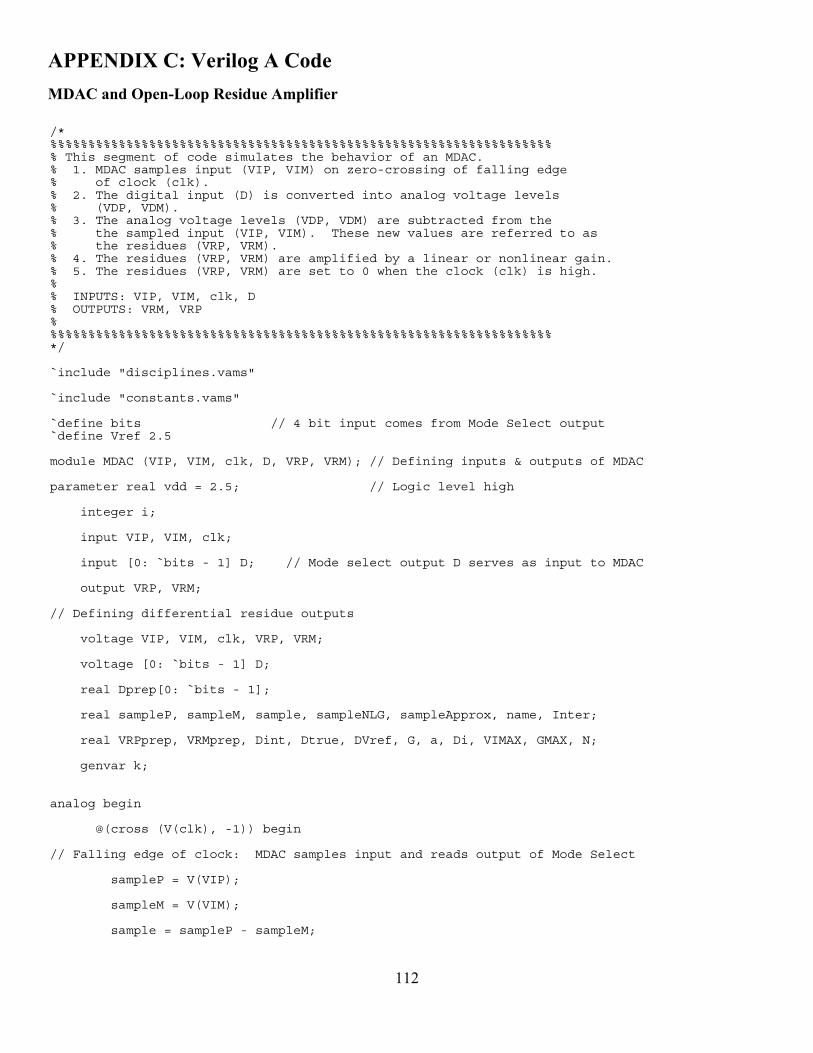
112
APPENDIX C: Verilog A Code MDAC and Open-Loop Residue Amplifier
/* %%%%%%%%%%%%%%%%%%%%%%%%%%%%%%%%%%%%%%%%%%%%%%%%%%%%%%%%%%%%%%%%%% % This segment of code simulates the behavior of an MDAC. % 1. MDAC samples input (VIP, VIM) on zero-crossing of falling edge % of clock (clk). % 2. The digital input (D) is converted into analog voltage levels % (VDP, VDM). % 3. The analog voltage levels (VDP, VDM) are subtracted from the % the sampled input (VIP, VIM). These new values are referred to as % the residues (VRP, VRM). % 4. The residues (VRP, VRM) are amplified by a linear or nonlinear gain. % 5. The residues (VRP, VRM) are set to 0 when the clock (clk) is high. % % INPUTS: VIP, VIM, clk, D % OUTPUTS: VRM, VRP % %%%%%%%%%%%%%%%%%%%%%%%%%%%%%%%%%%%%%%%%%%%%%%%%%%%%%%%%%%%%%%%%%% */ `include "disciplines.vams" `include "constants.vams" `define bits // 4 bit input comes from Mode Select output `define Vref 2.5 module MDAC (VIP, VIM, clk, D, VRP, VRM); // Defining inputs & outputs of MDAC parameter real vdd = 2.5; // Logic level high integer i; input VIP, VIM, clk; input [0: `bits - 1] D; // Mode select output D serves as input to MDAC output VRP, VRM; // Defining differential residue outputs voltage VIP, VIM, clk, VRP, VRM; voltage [0: `bits - 1] D; real Dprep[0: `bits - 1]; real sampleP, sampleM, sample, sampleNLG, sampleApprox, name, Inter; real VRPprep, VRMprep, Dint, Dtrue, DVref, G, a, Di, VIMAX, GMAX, N; genvar k; analog begin
@(cross (V(clk), -1)) begin // Falling edge of clock: MDAC samples input and reads output of Mode Select sampleP = V(VIP); sampleM = V(VIM); sample = sampleP - sampleM;

113
sampleNLG = sample; end for (k = 0; k < `bits; k = k + 1) begin Dprep[k] = V(D[k]); end @(cross (V(clk), 1)) begin // Rising edge of clock: MDAC calculates residue voltage Dint = 0; for (i = 0; i < `bits; i = i + 1) begin // Dint = Integer representation of Mode Select output if (Dprep[i] == 2.5) begin Dint = Dint + (pow(2,i)); end end Di = 5; // SET NUMBER OF DECISIONS HERE N = 15; // SET NUMBER OF QUANTIZER LEVELS AND ENSURE BITS DEFINED ABOVE CORRESPONDS! name = (Di - 1)/2; // name defines number of regions above and below zero region
sampleApprox = (-(`Vref) + (((2*Dint) - 1) / 2)*((2*`Vref)/N)); // sampleApprox: approximates the value of the original sample using the // quantizer output // Although the MDAC has the exact value of sample, the mode select and // quantizer combination // can cause the MDAC to take a different decision path // Equations for algorithm can be found in SN2 pgs. 89-92
for (i = 1; i <= name; i = i + 1) begin // Checks to see if sampleApprox is in one of the positive intervals // If it is, DVref and position on nonlinear curve are determined if ((sampleApprox > ((`Vref/Di)+((i-1)*((2*`Vref)/Di)))) && (sampleApprox <= ((`Vref/Di)+((i*2*`Vref)/Di)))) begin
DVref = (`Vref/Di)+((i-1)*((2*`Vref)/Di)) + (`Vref/Di);
sampleNLG = sampleNLG - DVref;
end end

114
for (i = 1; i <= name; i = i + 1) begin // Checks to see if sampleApprox is in one of the negative intervals if ((sampleApprox < ((-`Vref/Di)-((i-1)*((2*`Vref)/Di)))) && (sampleApprox >= ((-`Vref/Di)-((i*2*`Vref)/Di)))) begin DVref = ((-`Vref/Di)-((i*2*`Vref)/Di)) + (`Vref/Di); sampleNLG = sampleNLG - DVref; end end if ((sampleApprox <= (`Vref/Di)) && (sampleApprox >= (-`Vref/Di))) begin // Checks to see if sampleApprox is in the zero interval DVref = 0; sampleNLG = sampleNLG - DVref; end G = 3; // SET LINEAR GAIN OF DIFFERENTIAL PAIR HERE GMAX = G * 0.325; VIMAX = `Vref/Di; Inter = (GMAX/(3*G)); a = (0.3333 - Inter)*(pow((`Vref/VIMAX), 2)); // alpha parameter of nonlinear gain // VRPprep = 1.25 + (0.5*G*(sample - DVref)); // These two lines are for linear gain // VRMprep = 1.25 - (0.5*G*(sample - DVref)); VRPprep = 1.25 + (0.5*G*(sample - DVref)*(1 -a*(pow((sampleNLG/(`Vref)),2)))); // Nonlinear gain VRMprep = 1.25 - (0.5*G*(sample - DVref)*(1 -a*(pow((sampleNLG/(`Vref)),2)))); end V(VRP) <+ transition(VRPprep, 0, 1u); V(VRM) <+ transition(VRMprep, 0, 1u); end endmodule

115
Quantizer
/* %%%%%%%%%%%%%%%%%%%%%%%%%%%%%%%%%%%%%%%%%%%%%%%%%%%%%%%%%%%%%%%%%% % This segment of code simulates the behavior of an N-bit quantizer. % Values for the input voltage are correlated to an output level % on zero-crossings of the falling edge of the clock. % The N-Bit quantizer simulation uses a zero level. % Inputs: differential signals VIP and VIM, clk % Output: quantized value of input Q % % % Definitions: % N = number of quantization levels % Vref = maximum allowable input voltage % name = (N-2)/2 %%%%%%%%%%%%%%%%%%%%%%%%%%%%%%%%%%%%%%%%%%%%%%%%%%%%%%%%%%%%%%%%%% */ `include "disciplines.vams" `include "constants.vams" `define bits 4 // Need constants or constant expressions for genvar for loop, see pg. 40 SN2 `define Vref 2.5 module quantizerN (VIP, VIM, clk, Q); // Defining quantizer and its respective inputs/outputs parameter real vdd = 2.5; // Logic level HIGH for digital output integer i, N; input VIP, VIM, clk; // Differential inputs and clock output [0: `bits - 1] Q; // Quantized output value Q voltage VIP, VIM, clk; // Defining inputs VIP, VIM, and clock as voltages voltage [0: `bits - 1] Q; real Qprep[0: `bits - 1]; // Qprep is the output Q and is assigned as such in the last for loop real sampleP, sampleM, sample, result, copyresult, name; // sampleP = VIP, sampleM = VIM, sample = VIP-VIM, result = integer value of Q genvar k; // Loop variable used for making final assignment of Q analog begin @(cross (V(clk), -1)) begin // Quantizer activated on zero-crossing of negative edge of clock sampleP = V(VIP); sampleM = V(VIM); sample = sampleP - sampleM;
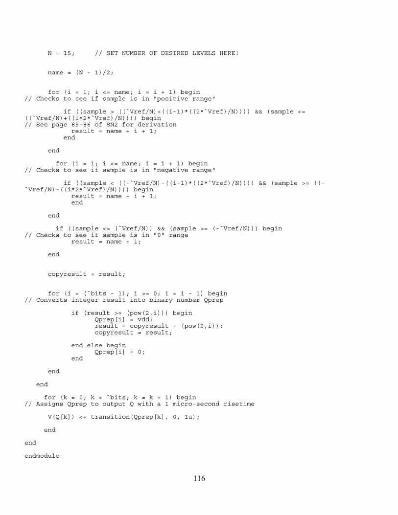
116
N = 15; // SET NUMBER OF DESIRED LEVELS HERE! name = (N - 1)/2; for (i = 1; i <= name; i = i + 1) begin // Checks to see if sample is in "positive range" if ((sample > ((`Vref/N)+((i-1)*((2*`Vref)/N)))) && (sample <= ((`Vref/N)+((i*2*`Vref)/N)))) begin // See page 85-86 of SN2 for derivation result = name + i + 1; end end for (i = 1; i <= name; i = i + 1) begin // Checks to see if sample is in "negative range" if ((sample < ((-`Vref/N)-((i-1)*((2*`Vref)/N)))) && (sample >= ((-`Vref/N)-((i*2*`Vref)/N)))) begin result = name - i + 1; end end if ((sample <= (`Vref/N)) && (sample >= (-`Vref/N))) begin // Checks to see if sample is in "0" range result = name + 1; end copyresult = result; for (i = (`bits - 1); i >= 0; i = i - 1) begin // Converts integer result into binary number Qprep if (result >= (pow(2,i))) begin Qprep[i] = vdd; result = copyresult - (pow(2,i)); copyresult = result; end else begin Qprep[i] = 0; end end end for (k = 0; k < `bits; k = k + 1) begin // Assigns Qprep to output Q with a 1 micro-second risetime V(Q[k]) <+ transition(Qprep[k], 0, 1u); end end endmodule

117
Mode Select
%%%%%%%%%%%%%%%%%%%%%%%%%%%%%%%%%%%%%%%%%%%%%%%%%%%%%%%%%%%%%%%%%% /* Mode Select % % This segment of code simulates the behavior of a Mode Select. % 1. M = 0: Mode select passes Q input from Quantizer to output D. % 2. M = 1: Mode select adds one to input Q to produce output D. % % INPUTS: Q, M % OUTPUTS: D % %%%%%%%%%%%%%%%%%%%%%%%%%%%%%%%%%%%%%%%%%%%%%%%%%%%%%%%%%%%%%%%%%% */ `include "disciplines.vams" `include "constants.vams" `define bits 4 // Number of bits for D and Q `define Vref 2.5 // Maximum input voltage to any stage module ModeSelect (Q, M, D); parameter real vdd = 2.5; // Logic level high integer i; input M; // M = control signal for Mode Select input [0: `bits - 1] Q; // Q = output of Quantizer output [0: `bits - 1] D; // D = input to MDAC voltage M; voltage [0: `bits - 1] Q; voltage [0: `bits - 1] D; real Dprep[0: `bits - 1]; // Will be used to hold intermediate value of D real Qprep[0: `bits - 1]; // Will be used to hold intermediate value of Q real Mvalue, Qint; // Qint = decimal value of Q, Mvalue holds value of M genvar k; analog begin Mvalue = V(M); // Mvalue obtains value of control signal M for (k = 0; k < `bits; k = k + 1) begin // Copy value of input to Qprep Qprep[k] = V(Q[k]); end

118
if (Mvalue == 0) begin // If control signal = 0V for (i = 0; i < `bits; i = i + 1) begin // Value of Q goes to value of D untouched Dprep[i] = Qprep[i]; end end if (Mvalue == 2.5) begin // If control signal = 2.5V Qint = 0; // Qint will hold decimal value of Q for (i = 0; i < `bits; i = i + 1) begin // Find decimal value of Q if (Qprep[i] == 2.5) begin Qint = Qint + (pow(2,i)); end end Qint = Qint - 1; // Subtract 1 from decimal value of Q for (i = (`bits - 1); i >= 0; i = i - 1) begin // Convert decimal value of Q back to a binary number if (Qint >= (pow(2,i))) begin Dprep[i] = vdd; Qint = Qint - (pow(2,i)); end else begin Dprep[i] = 0; end end end for (k = 0; k < `bits; k = k + 1) begin // D equals current value of Dprep with 1 micro-second transition V(D[k]) <+ transition(Dprep[k], 0, 1u); end end endmodule

119
APPENDIX D: Behavioral Simulation Results

120

121

122

123

124

125

126
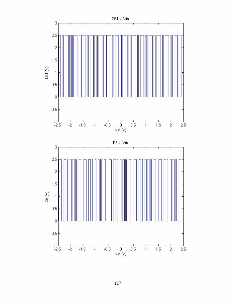
127

128

129

130
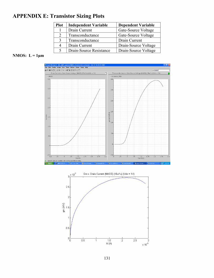
131
APPENDIX E: Transistor Sizing Plots Plot Independent Variable Dependent Variable
1 Drain Current Gate-Source Voltage 2 Transconductance Gate-Source Voltage 3 Transconductance Drain Current 4 Drain Current Drain-Source Voltage 5 Drain-Source Resistance Drain-Source Voltage
NMOS: L = 1μm

132
NMOS: L = 1μm
NMOS: L = 0.18μm

133

134
NMOS: L = 0.36μm

135
PMOS: L = 1μm

136
1.00E-09
1.00E-08
1.00E-07
1.00E-06
1.00E-05
1.00E-04
1.00E-03
1.00E-02
1.00E-01
1.00E+00
1.00E-10 1.00E-08 1.00E-06 1.00E-04 1.00E-02 1.00E+00
Gm
(A/V
)
Id (A)
PMOS 18u/1u Gm vs. Id
`

137
PMOS: L = 0.18μm

138
PMOS: L = 0.36μm

139
1.00E-09
1.00E-08
1.00E-07
1.00E-06
1.00E-05
1.00E-04
1.00E-03
1.00E-02
1.00E-01
1.00E+00
1.00E-11 1.00E-09 1.00E-07 1.00E-05 1.00E-03 1.00E-01
Gm
(A/V
)
Id (A)
PMOS 18u/0.36u Gm vs. Id
`

140
APPENDIX F: 31-Level Quantizer Verification
Table 13: 31-Level Quantizer Verification

141
Figure 91: 31-Level Quantizer Verification
0
0.2
0.4
0.6
0.8
1
1.2
1.4
1.6
2.0E‐9 12.8E‐9 22.5E‐9 32.7E‐9 41.9E‐9 53.0E‐9 62.7E‐9 72.1E‐9 82.2E‐9 92.8E‐9
Voltage
(V)
Time (sec)
31‐Level Quantizer Verification
VINP VINM d0 d1 d2 d3 d4
d5 d6 d7 d8 d9 d10 d11
d12 d13 d14 d15 d16 d17 d18
d19 d20 d21 d22 d23 d24 d25
d26 d27 d28 d29 d30
Related Documents


