8085 Architecture AKHIL C 12MT06PED001

Welcome message from author
This document is posted to help you gain knowledge. Please leave a comment to let me know what you think about it! Share it to your friends and learn new things together.
Transcript
8085 Architecture
AKHIL C
12MT06PED001

Microprocessor
• A microprocessor is an electronic device that reads binary instructions from a storage device called memory, accepts binary data as input, processes data according to those instructions, and provides results as output.

Microprocessor• A microprocessor may be thought of as a silicon chip
around which a microcomputer is built.
• A general purpose microprocessor must add RAM,ROM,I/O Ports, and timers externally to make them functional.

8085 Microprocessor
• The 8085 Microprocessor was made by Intel in mid 1970s.
• It is an 8 bit general purpose microprocessor.
• It is capable of addressing 64k of memory.
• Requires +5V power supply.
• Can operate with 3MHz clock.
• Has 40 pins
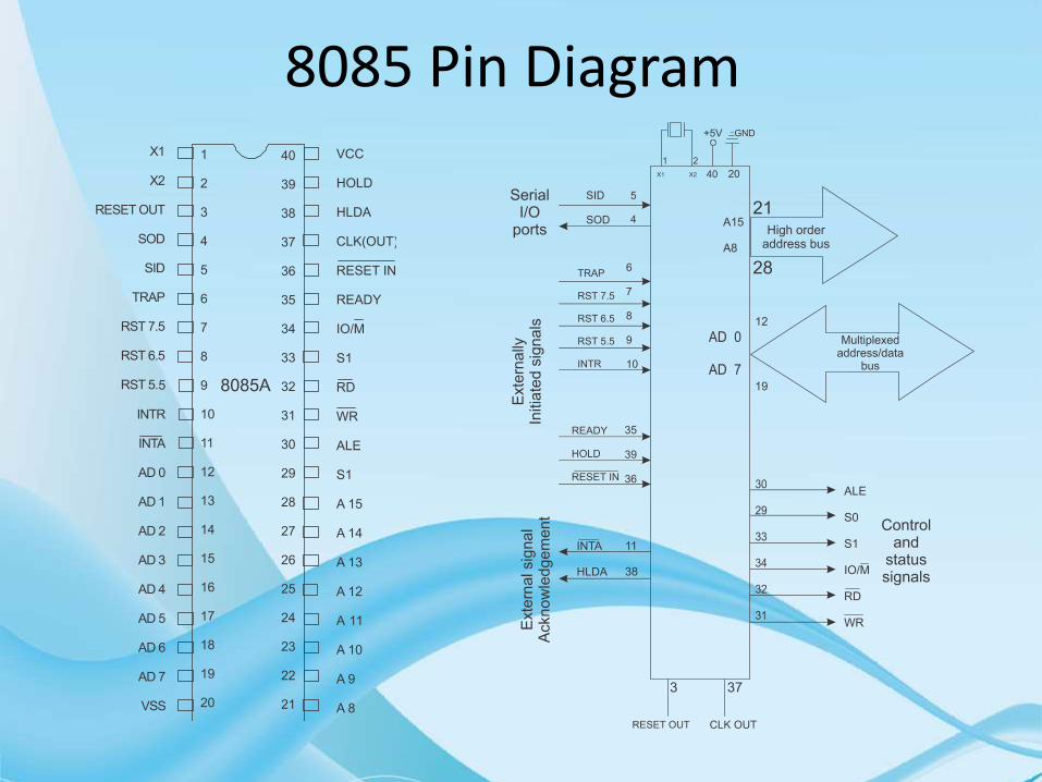
8085 Pin Diagram

8085 System Bus• The microprocessor performs four operations primarily:
• Memory Read
• Memory Write
• I/O Read
• I/O Write
• The 8085 performs these operations using three sets of communication lines called buses, they are:
• The address bus
• The data bus
• The Control and Status bus

8085 System Bus• Address Bus
• It is a group of 16 lines (A15 –A8 and AD7-AD0)
• It is unidirectional. From 8085 to peripheral devices.
• The 8085 identify peripherals or memory location using the address bus.
• With the 16 lines, 8085 is capable of addressing 64K memory locations.
• Among these 16 lines, the lower order 8 lines are time multiplexed address/data bus.
• While addressing a memory location 8 most significant bits of the 16 bit address are transmitted with the help of higher order address bus while the 8 least significant bits are transmitted with the help of multiplexed address/data bus.
8085 System Bus
• Data Bus• It is a group of 8 lines. (AD7-AD0)
• It is used for data flow.
• It is bidirectional
• With these 8 lines the 8085 is capable to manipulate 8-bit data ranging from 00 to FF.
• In executing an instruction, during the earlier part of the cycle, these lines are used as the low order address bus. During the later part of the cycle, these lines are used as the data bus.

8085 System Bus
• Control and Status Bus• It consists of various single lines that carry the
synchronizing signals.
• They are not group of lines.
• These individual lines provide a pulse to indicate an operation.
• 8085 generates specific control signal for each operation it performs.
• 8085 uses these signals to identify the type of device it intends to communicate.
Control and Status Signals
• Two Control Signals (RD and WR)
• Three Status Signals (IO/M , S1 and S0)
• One special signal (ALE)
• RD : Read:-This is the Read control signal(active low). This signal indicates that the selected I/O or memory device is to be read and data are available on the data bus.
• WR: Write:-This is the Write control signal(active low). This signal indicates that the data on the data bus are to be written into selected memory or I/O location.

Control and Status Signals• IO/M : This is a status signal used to differentiate between
I/O and memory operations. When it is high, it indicates an I/O operation & when it is low, it indicates a memory operation. This signal is combined with RD and WR to generate I/O and memory control signals.
• S1 and S0 : These are status signals, similar to IO/M can identify various operations, but they are rarely used in small system.
S0 S1 STATE
0 0 HALT
0 1 READ
1 0 WRITE
1 1 FETCH

Power Supply and Frequency Signals
• VCC : +5 V power supply.
• VSS : Ground Reference.
• X1, X2 : A crystal is connected at these two pins. The frequency is internally divided by two; therefore, to operate a system at 3MHz, the crystal should have a frequency of 6MHz.
• CLK(OUT)-Clock Output: this signal can be used as the system clock for other devices.
Control and Status Signals
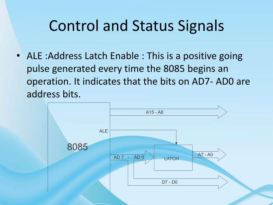
• ALE :Address Latch Enable : This is a positive going pulse generated every time the 8085 begins an operation. It indicates that the bits on AD7- AD0 are address bits.
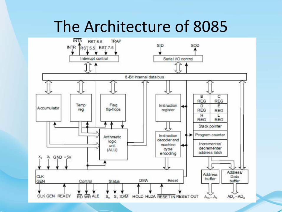
The Architecture of 8085

Various functional blocks of 8085
• Registers
• Arithmetic Logic Unit
• Address buffer and Address data buffer
• Incrementer/ Decrementer address latch
• Interrupt Control
• Serial I/O Control
• Timing and Control Circuitry
• Instructions decoder and machine cycle encoder
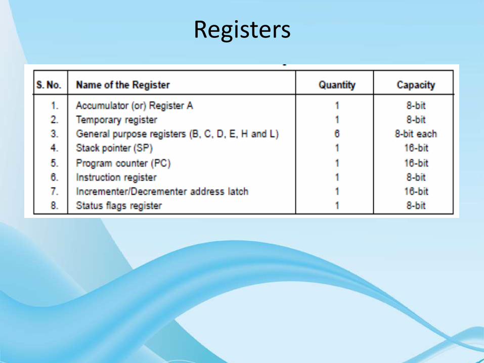
Registers
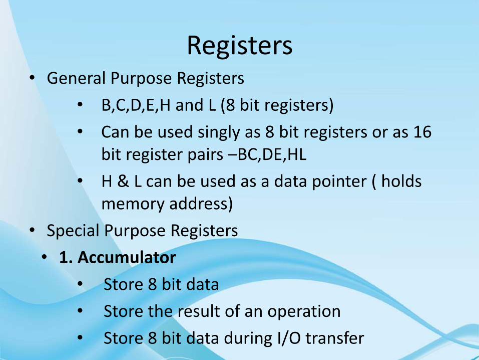
Registers• General Purpose Registers
• B,C,D,E,H and L (8 bit registers)
• Can be used singly as 8 bit registers or as 16 bit register pairs –BC,DE,HL
• H & L can be used as a data pointer ( holds memory address)
• Special Purpose Registers
• 1. Accumulator
• Store 8 bit data
• Store the result of an operation
• Store 8 bit data during I/O transfer
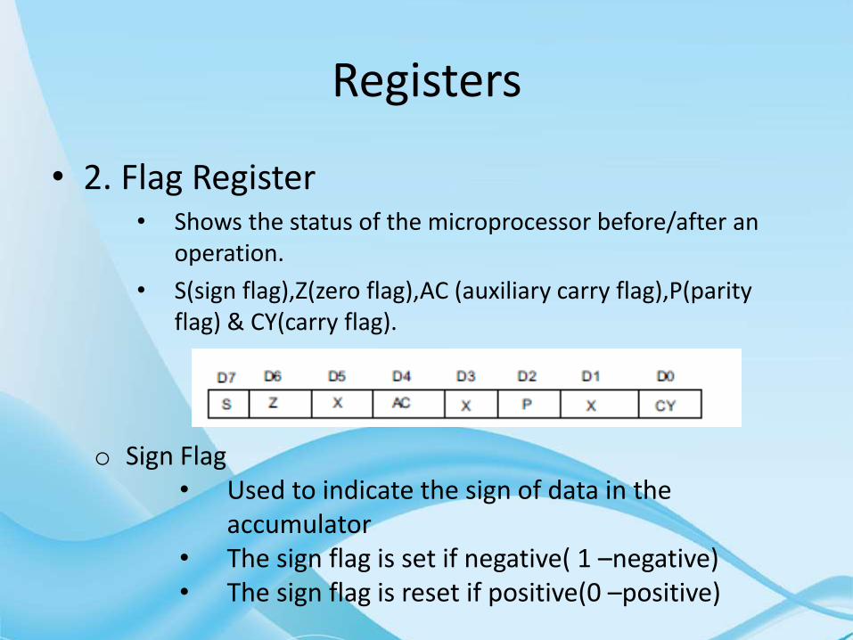
Registers
• 2. Flag Register• Shows the status of the microprocessor before/after an
operation.
• S(sign flag),Z(zero flag),AC (auxiliary carry flag),P(parity flag) & CY(carry flag).
o Sign Flag• Used to indicate the sign of data in the
accumulator • The sign flag is set if negative( 1 –negative)• The sign flag is reset if positive(0 –positive)
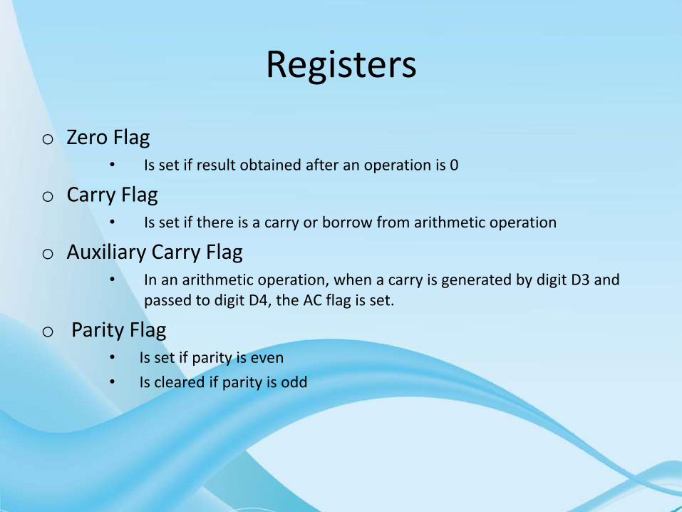
Registers
o Zero Flag• Is set if result obtained after an operation is 0
o Carry Flag • Is set if there is a carry or borrow from arithmetic operation
o Auxiliary Carry Flag• In an arithmetic operation, when a carry is generated by digit D3 and
passed to digit D4, the AC flag is set.
o Parity Flag• Is set if parity is even
• Is cleared if parity is odd

Registers
• Temporary Registers• It is an 8 bit data register.• It is not available to the programmer • Is used internally for execution of most of the arithmetic
and logic operations.
• Stack Pointer(SP)• It is a 16 bit register used to point into memory.• The memory this register points to is a special area called
stack• The stack is an area of memory used to hold data that will
be retrieved soon • The stack is usually accessed in a Last in First out (LIFO)
fashion.

Register
• Program Counter(PC)• Used to control the sequencing of the execution of instructions.• This register always holds the address of the next instruction.• Since it holds an address, it must be 16 bits wide.
• Instruction Register(IR)• Instruction is stored in IR after fetched by processor• Decoder decodes instruction in IR• The instruction register is not programmable and cannot be
accessed through any instruction.
• Incrementer/Decrementer address latch register• It is a 16 bit register increments/decrements the contents of PC
or SP when instructions related to them are executed.
Arithmetic Logic Unit
• The ALU performs the actual numerical and logic operations such as ‘add’, ‘subtract’, ‘AND’, ‘OR’, etc.
• It uses data from memory and from accumulator to perform these calculations.
• Always stores result of operations in the accumulator.
• The temporary register used for holding data temporarily during execution of an operation is part of the ALU.

Address buffer and Address Data buffer
• The contents of the stack pointer and program counter are loaded into the address buffer and address data buffer.
• These buffers are then used to drive the external address bus and address data bus.
• As the memory and I/O chips are connected to these buses, the CPU can exchange desired data to the memory and I/O chips.
• The address data buffer is not only connected to the external data bus but also to the internal data bus which consists of 8 bits.
• The address data buffer can both send and receive data from internal data bus.
Interrupt Control
• As the name suggests this is to interrupt a process.• Consider that a microprocessor is executing the main
program.• Now whenever the interrupt signal is enabled or requested
the microprocessor shifts the control from main program to the incoming request and after the completion of request, the control goes back to the main program.
• For example an I/O device may send an interrupt signal to notify that the data is ready for input.
• The microprocessor temporarily stops the execution of main program and transfers control to I/O device.
• After collecting the input data the control is transferred back to main program.

8085 Interrupts
• The 8085 has 5 interrupt signals that can be used to interrupt a program execution.
• INTA : Interrupt Acknowledge, This signal is used to acknowledge an interrupt.
Externally Initiated Signals, Including Interrupts
• TRAP is a non-maskable interrupt ,while all other are maskable.
• Non- maskable interrupt is given the highest priority in the order of interrupt. It cannot be disabled by the programmer at any point of time.
• Maskable interrupts can be disabled by the programmer using EI and DI instructions. Among maskable interrupts RST 7.5 is given the highest priority above RST 6.5 and least priority is given to INTR.
Externally Initiated Signals, Including Interrupts
• HOLD (Input) : This signal indicates that a peripheral such as a DMA (Direct Memory Access) controller is requesting the use of the address and data buses.
• HLDA(Output) : Hold Acknowledge: This signal acknowledges the HOLD request.
• READY(Input) This signal is used to delay the microprocessor Read or Write cycles until a slow responding peripheral is ready to send or accept data. When this signal goes low, the microprocessor waits for an integral number of clock cycles until it goes high.

Externally Initiated Signals, Including Interrupts
• RESET IN : When the signal on this pin goes low, the program counter is set to zero, the buses are tri-stated , and the MPU is reset.
• RESET OUT : This signal indicates that the MPU is being reset. This signal can be used to reset other devices.
Serial I/O Control
• 8085 has serial I/O control via its SOD(Serial Output Data) and SID( Serial Input Data) pins. (pin 4 and 5).
• These pins allow 8085 to communicate serially with external devices.
• In serial transmission, data bits are sent over a single line, one bit at a time, such as the transmission over telephone lines.
Timing & Control Unit
• The timing & control unit of the 8085 is responsible for:
• Timing of all components (within and outside the microprocessor)
• Clock input
• Input and Output traffic flow on all busses
• External inputs (for example, reset)
• External outputs (for example, status)
• It ensures proper traffic flow on all buses

Related Documents


![RESET/ENABLE DIAGRAMCPU, FSB [PAGE_TITLE=CPU, FSB] XENON_RETAIL 5/73 K7 12 12 12 12 12 12 12 12 12 12 12 12 12 12 12 12 12 12 12 12 12 12 12 12 12 12 12 12 12 12 12 12 12 12 12 12](https://static.cupdf.com/doc/110x72/610d0b50d45ff058ad2eca90/resetenable-diagram-cpu-fsb-pagetitlecpu-fsb-xenonretail-573-k7-12-12-12.jpg)