BurrĆBrown Products from Texas Instruments DAC7821 FEATURES DESCRIPTION APPLICATIONS DAC Register Power-On Reset Control Logic DAC7821 R R FB V REF V DD I 1 OUT I 2 OUT GND DB0 DB11 12-Bit R-2R DAC Input Latch Parallel Bus CS R/W DAC7821 SBAS365B – OCTOBER 2005 – REVISED JULY 2007 12-Bit, Parallel Input, Multiplying Digital-to-Analog Converter • 2.5V to 5.5V Supply Operation The DAC7821 is a CMOS 12-bit current output digital-to-analog converter (DAC). This device • Fast Parallel Interface: operates from a single 2.5V to 5.5V power supply, 17ns Write Cycle making it suitable for battery-powered and many • Update Rate of 20.4MSPS other applications. • 10MHz Multiplying Bandwidth This DAC operates with a fast parallel interface. Data • ±10V Reference Input readback allows the user to read the contents of the • Low Glitch Energy: 5nV-s DAC register via the DB pins. On power-up, the internal register and latches are filled with zeroes • Extended Temperature Range: and the DAC outputs are at zero scale. –40°C to +125°C The DAC7821 offers excellent 4-quadrant • 20-Lead TSSOP Packages multiplication characteristics, with a large signal • 12-Bit Monotonic multiplying bandwidth of 10MHz. The applied • ±1LSB INL external reference input voltage (V REF ) determines • 4-Quadrant Multiplication the full-scale output current. An integrated feedback resistor (R FB ) provides temperature tracking and • Power-On Reset with Brownout Detection full-scale voltage output when combined with an • Readback Function external current-to-voltage precision amplifier. • Industry-Standard Pin Configuration The DAC7821 is available in a 20-lead TSSOP package. • Portable Battery-Powered Instruments • Waveform Generators • Analog Processing • Programmable Amplifiers and Attenuators • Digitally-Controlled Calibration • Programmable Filters and Oscillators • Composite Video • Ultrasound Please be aware that an important notice concerning availability, standard warranty, and use in critical applications of Texas Instruments semiconductor products and disclaimers thereto appears at the end of this data sheet. All trademarks are the property of their respective owners. PRODUCTION DATA information is current as of publication date. Copyright © 2005–2007, Texas Instruments Incorporated Products conform to specifications per the terms of the Texas Instruments standard warranty. Production processing does not necessarily include testing of all parameters.

Welcome message from author
This document is posted to help you gain knowledge. Please leave a comment to let me know what you think about it! Share it to your friends and learn new things together.
Transcript

DAC7821
FEATURES DESCRIPTION
APPLICATIONS
DAC Register
Power-On
Reset
Control
Logic
DAC7821R
RFB
VREFVDD
I 1OUT
I 2OUT
GND
DB0 DB11
12-Bit
R-2R DAC
Input Latch
Parallel Bus
CS
R/W
DAC7821
SBAS365B–OCTOBER 2005–REVISED JULY 2007
12-Bit, Parallel Input, MultiplyingDigital-to-Analog Converter
• 2.5V to 5.5V Supply Operation The DAC7821 is a CMOS 12-bit current outputdigital-to-analog converter (DAC). This device• Fast Parallel Interface:operates from a single 2.5V to 5.5V power supply,17ns Write Cyclemaking it suitable for battery-powered and many• Update Rate of 20.4MSPSother applications.
• 10MHz Multiplying BandwidthThis DAC operates with a fast parallel interface. Data• ±10V Reference Input readback allows the user to read the contents of the
• Low Glitch Energy: 5nV-s DAC register via the DB pins. On power-up, theinternal register and latches are filled with zeroes• Extended Temperature Range:and the DAC outputs are at zero scale.–40°C to +125°CThe DAC7821 offers excellent 4-quadrant• 20-Lead TSSOP Packagesmultiplication characteristics, with a large signal• 12-Bit Monotonicmultiplying bandwidth of 10MHz. The applied
• ±1LSB INL external reference input voltage (VREF) determines• 4-Quadrant Multiplication the full-scale output current. An integrated feedback
resistor (RFB) provides temperature tracking and• Power-On Reset with Brownout Detectionfull-scale voltage output when combined with an• Readback Function external current-to-voltage precision amplifier.
• Industry-Standard Pin ConfigurationThe DAC7821 is available in a 20-lead TSSOPpackage.
• Portable Battery-Powered Instruments• Waveform Generators• Analog Processing• Programmable Amplifiers and Attenuators• Digitally-Controlled Calibration• Programmable Filters and Oscillators• Composite Video• Ultrasound
Please be aware that an important notice concerning availability, standard warranty, and use in critical applications of TexasInstruments semiconductor products and disclaimers thereto appears at the end of this data sheet.
All trademarks are the property of their respective owners.
PRODUCTION DATA information is current as of publication date. Copyright © 2005–2007, Texas Instruments IncorporatedProducts conform to specifications per the terms of the TexasInstruments standard warranty. Production processing does notnecessarily include testing of all parameters.

www.ti.com
PACKAGE/ORDERING INFORMATION
ABSOLUTE MAXIMUM RATINGS
DAC7821
SBAS365B–OCTOBER 2005–REVISED JULY 2007
This integrated circuit can be damaged by ESD. Texas Instruments recommends that all integrated circuits be handled withappropriate precautions. Failure to observe proper handling and installation procedures can cause damage.
ESD damage can range from subtle performance degradation to complete device failure. Precision integrated circuits may bemore susceptible to damage because very small parametric changes could cause the device not to meet its publishedspecifications.
For the most current package and ordering information, see the Package Option Addendum at the end of thisdocument, or see the TI website at www.ti.com.
over operating free-air temperature range (unless otherwise noted) (1)
DAC7821 UNIT
VDD to GND –0.3 to +7 V
Digital input voltage to GND –0.3 to VDD + 0.3 V
V(IOUT) to GND –0.3 to VDD + 0.3 V
Operating temperature range –40 to +125 °C
Storage temperature range –65 to +150 °C
Junction temperature (TJ max) +150 °C
ESD Rating, HBM 3000 V
ESD Rating, CDM 1000 V
(1) Stresses above those listed under absolute maximum ratings may cause permanent damage to the device. Exposure to absolutemaximum conditions for extended periods may affect device reliability.
2 Submit Documentation Feedback

www.ti.com
ELECTRICAL CHARACTERISTICS
DAC7821
SBAS365B–OCTOBER 2005–REVISED JULY 2007
VDD = +2.5V to +5.5V; IOUT1 = Virtual GND; IOUT2 = 0V; VREF = +10V; TA = full operating temperature. All specifications –40°Cto +125°C, unless otherwise noted.
DAC7821
PARAMETER CONDITIONS MIN TYP MAX UNITS
STATIC PERFORMANCE
Resolution 12 Bits
Relative accuracy ±1 LSB
Differential nonlinearity ±1 LSB
Output leakage current Data = 000h, TA = +25°C ±10 nA
Output leakage current Data = 000h, TA = TMAX ±20 nA
Full-scale gain error All is loaded to DAC register ±5 ±10 mV
Full-scale tempco ±5 ppm/°C
Output capacitance Code dependent 30 pF
REFERENCE INPUT
VREF range –15 15 V
Input resistance 8 10 12 kΩ
RFB resistance 8 10 12 kΩ
LOGIC INPUTS AND OUTPUT (1)
Input low voltage VIL VDD = +2.7V 0.6 V
VIL VDD = +5V 0.8 V
Input high voltage VIH VDD = +2.7V 2.1 V
VIH VDD = +5V 2.4 V
Input leakage current IIL 10 µA
Input capacitance CIL 10 pF
POWER REQUIREMENTS
VDD 2.7 5.5 V
IDD (normal operation) Logic inputs = 0V 5 µA
VDD = +4.5V to +5.5V VIH = VDD and VIL = GND 0.8 5 µA
VDD = +2.5V to +3.6V VIH = VDD and VIL = GND 0.4 2.5 µA
AC CHARACTERISTICS
Output voltage settling time 0.2 µs
Reference multiplying BW VREF = 7VPP, Data = FFFh 10 MHz
VREF = 0V to 10V,DAC glitch impulse 5 nV-sData = 7FFh to 800h to 7FFh
Feedthrough error VOUT/VREF Data = 000h, VREF = 100kHz –70 dB
Digital feedthrough 2 nV-s
Total harmonic distortion –105 dB
Output spot noise voltage 18 nV/√Hz
(1) Specified by design and characterization; not production tested.
3Submit Documentation Feedback

www.ti.com
DATA VALID DATA VALID
R/W
CS
DATA
t1 t2 t2
t3
t4t5
t6
t7
t8 t9
TIMING REQUIREMENTS: 2.5 V to 4.5 V
TIMING REQUIREMENTS: 4.5 V to 5.5 V
DAC7821
SBAS365B–OCTOBER 2005–REVISED JULY 2007
TIMING INFORMATION
At tr = tf = 1ns (10% to 90% of VDD) and timed from a voltage level of (VIL + VIH)/2; VDD = +2.5V to +4.5V, VREF = +10V,IOUT2 = 0V. All specifications –40°C to +125°C, unless otherwise noted.
DAC7821
PARAMETER (1) TEST CONDITIONS MIN TYP MAX UNIT
t1 R/W to CS setup time 0 ns
t2 R/W to CS hold time 0 ns
t3 CS low time (write cycle) 10 ns
t4 Data setup time 6 ns
t5 Data hold time 0 ns
t6 R/W high to CS low 5 ns
t7 CS min high time 9 ns
t8 Data access time 20 40 ns
t9 Bus relinquish time 5 10 ns
(1) Ensured by design; not production tested.
At tr = tf = 1ns (10% to 90% of VDD) and timed from a voltage level of (VIL + VIH)/2; VDD = +4.5V to +5.5V, VREF = +10V,IOUT2 = 0V. All specifications –40°C to +125°C, unless otherwise noted.
DAC7821
PARAMETER (1) TEST CONDITIONS MIN TYP MAX UNIT
t1 R/W to CS setup time 0 ns
t2 R/W to CS hold time 0 ns
t3 CS low time (write cycle) 10 ns
t4 Data setup time 6 ns
t5 Data hold time 0 ns
t6 R/W high to CS low 5 ns
t7 CS min high time 7 ns
t8 Data access time 10 20 ns
t9 Bus relinquish time 5 10 ns
(1) Ensured by design; not production tested.
4 Submit Documentation Feedback

www.ti.com
DEVICE INFORMATION
1
2
3
4
5
6
7
8
9
10
20
19
18
17
16
15
14
13
12
11
GND
DB11 (MSB)
DB10
DB9
DB8
DB7
DB6
DB5
DB0 (LSB)
DB1
DB2
DB3
DB4
DAC7821
TSSOP-20
I 1OUT RFB
VREF
VDD
I 2OUT
R/W
CS
DAC7821
SBAS365B–OCTOBER 2005–REVISED JULY 2007
TERMINAL FUNCTIONS
TERMINAL
TSSOPNO. NAME DESCRIPTION
1 IOUT1 DAC current output.
2 IOUT2 DAC analog ground. This pin is normally tied to the analog ground of the system.
3 GND Ground pin.
4–15 DB11 – DB0 Parallel data bits 11 to 0.
Chip select input. Active low. Used in conjunction with R/W to load parallel data to the input latch or16 CS read data from the DAC register. Rising edge of CS loads data.
Read/Write. When low, use in conjunction with CS to load parallel data. When high, use with CS to17 R/W read back contents of DAC register.
18 VDD Positive power supply input. These parts can be operated from a supply of 2.5V to 5.5V.
19 VREF DAC reference voltage input.
DAC feedback resistor pin. Establish voltage output for the DAC by connecting to external amplifier20 RFB output.
5Submit Documentation Feedback

www.ti.com
TYPICAL CHARACTERISTICS: VDD = +5V
1.0
0.8
0.6
0.4
0.2
0
0.2
0.4
0.6
0.8
1.0
-
-
-
-
-
INL (
LS
B)
0 512 1024 1536 2048 2560 3072 3584 4095
T = +25 CA °
V = 10 VREF +
Digital Input Code
1.0
0.8
0.6
0.4
0.2
0
0.2
0.4
0.6
0.8
1.0
-
-
-
-
-
DN
L (
LS
B)
0 512 1024 1536 2048 2560 3072 3584 4095
T = +25 CA °
V = 10 VREF +
Digital Input Code
1.0
0.8
0.6
0.4
0.2
0
0.2
0.4
0.6
0.8
1.0
-
-
-
-
-
INL (
LS
B)
0 512 1024 1536 2048 2560 3072 3584 4095
T = 40 CA - °
V = 10 VREF +
Digital Input Code
1.0
0.8
0.6
0.4
0.2
0
0.2
0.4
0.6
0.8
1.0
-
-
-
-
-
DN
L (
LS
B)
0 512 1024 1536 2048 2560 3072 3584 4095
T = 40 CA - °
V = 10 VREF +
Digital Input Code
1.0
0.8
0.6
0.4
0.2
0
0.2
0.4
0.6
0.8
1.0
-
-
-
-
-
INL (
LS
B)
0 512 1024 1536 2048 2560 3072 3584 4095
T = +125 CA °
V = 10 VREF +
Digital Input Code
1.0
0.8
0.6
0.4
0.2
0
0.2
0.4
0.6
0.8
1.0
-
-
-
-
-
DN
L (
LS
B)
0 512 1024 1536 2048 2560 3072 3584 4095
T = +125 CA °
V = 10 VREF +
Digital Input Code
DAC7821
SBAS365B–OCTOBER 2005–REVISED JULY 2007
At TA = +25°C, unless otherwise noted.
LINEARITY ERROR DIFFERENTIAL LINEARITY ERRORvs DIGITAL INPUT CODE vs DIGITAL INPUT CODE
Figure 1. Figure 2.
LINEARITY ERROR DIFFERENTIAL LINEARITY ERRORvs DIGITAL INPUT CODE vs DIGITAL INPUT CODE
Figure 3. Figure 4.
LINEARITY ERROR DIFFERENTIAL LINEARITY ERRORvs DIGITAL INPUT CODE vs DIGITAL INPUT CODE
Figure 5. Figure 6.
6 Submit Documentation Feedback

www.ti.com
3.0
2.5
2.0
1.5
1.0
0.5
0
Supply
Curr
ent (m
A)
0 0.5 1.0 1.5 2.0 2.5 3.0 3.5 4.0 4.5 5.0
Logic Input Voltage (V)
V = 2.5 VDD
V = 3.0 VDD
V = 5.0 VDD
606
121824303642485660667278849096
102-
-
-
-
-
-
-
-
-
-
-
-
-
-
-
-
-
0xFFF0x8000x4000x2000x1000x0800x0400x0200x0100x0080x0040x0020x001
Attenuation (
dB
)
10 100 1k 10k 100k 1M 10M 100M
Bandwidth (Hz)
0x000
Outp
ut V
oltage (
50m
V/d
iv)
Code 2047 to 2048
DAC Update
Time (50ns/div) Time (50ns/div)
Outp
ut V
oltage (
50m
V/d
iv)
Code 2048 to 2047
DAC Update
Time (20 ns/div)
Outp
ut V
oltage (
%)
Small Signal Settling
DAC Update
10
90
V = I x 100 WOUT OUT
Gain
Err
or
(mV
)
0
0.2
0.4
0.6
0.8
1.0
1.2
1.4
1.6
1.8
-2.0
-
-
-
-
-
-
-
-
-
-
-40 -20 0 20 40 60 80 100 120
Temperature ( C)°
V = +10 VREF
DAC7821
SBAS365B–OCTOBER 2005–REVISED JULY 2007
TYPICAL CHARACTERISTICS: VDD = +5V (continued)At TA = +25°C, unless otherwise noted.
SUPPLY CURRENTvs LOGIC INPUT VOLTAGE REFERENCE MULTIPLYING BANDWIDTH
Figure 7. Figure 8.
MIDSCALE DAC GLITCH MIDSCALE DAC GLITCH
Figure 9. Figure 10.
GAIN ERRORDAC SETTLING TIME vs TEMPERATURE
Figure 11. Figure 12.
7Submit Documentation Feedback

www.ti.com
2.0
1.8
1.6
1.4
1.2
1.0
0.8
0.6
0.4
0.2
0
Quie
scent C
urr
ent (
A)
m
-40 -20 0 20 40 60 80 100 120
Temperature ( C)°
V = +10 VREF
V = +2.5 VDD
V = +5.0 VDD
Leakage C
urr
ent (n
A)
0.2
0.18
0.16
0.14
0.12
0.10
0.08
0.06
0.04
0.02
0
-40 -20 0 20 40 60 80 100 120
Temperature ( C)°
DAC7821
SBAS365B–OCTOBER 2005–REVISED JULY 2007
TYPICAL CHARACTERISTICS: VDD = +5V (continued)At TA = +25°C, unless otherwise noted.
SUPPLY CURRENT LEAKAGE CURRENTvs TEMPERATURE vs TEMPERATURE
Figure 13. Figure 14.
8 Submit Documentation Feedback

www.ti.com
TYPICAL CHARACTERISTICS: VDD = +2.5V
1.0
0.8
0.6
0.4
0.2
0
0.2
0.4
0.6
0.8
1.0
-
-
-
-
-
INL (
LS
B)
0 512 1024 1536 2048 2560 3072 3584 4095
T = +25 CA °
V = 10 VREF +
Digital Input Code
1.0
0.8
0.6
0.4
0.2
0
0.2
0.4
0.6
0.8
1.0
-
-
-
-
-
DN
L (
LS
B)
0 512 1024 1536 2048 2560 3072 3584 4095
T = +25 CA °
V = 10 VREF +
Digital Input Code
1.0
0.8
0.6
0.4
0.2
0
0.2
0.4
0.6
0.8
1.0
-
-
-
-
-
INL (
LS
B)
0 512 1024 1536 2048 2560 3072 3584 4095
T = 40 CA - °
V = 10 VREF +
Digital Input Code
1.0
0.8
0.6
0.4
0.2
0
0.2
0.4
0.6
0.8
1.0
-
-
-
-
-
DN
L (
LS
B)
0 512 1024 1536 2048 2560 3072 3584 4095
T = 40 CA - °
V = 10 VREF +
Digital Input Code
1.0
0.8
0.6
0.4
0.2
0
0.2
0.4
0.6
0.8
1.0
-
-
-
-
-
INL (
LS
B)
0 512 1024 1536 2048 2560 3072 3584 4095
T = +125 CA °
V = 10 VREF +
Digital Input Code
1.0
0.8
0.6
0.4
0.2
0
0.2
0.4
0.6
0.8
1.0
-
-
-
-
-
DN
L (
LS
B)
0 512 1024 1536 2048 2560 3072 3584 4095
T = +125 CA °
V = 10 VREF +
Digital Input Code
DAC7821
SBAS365B–OCTOBER 2005–REVISED JULY 2007
At TA = +25°C, unless otherwise noted.
LINEARITY ERROR DIFFERENTIAL LINEARITY ERRORvs DIGITAL INPUT CODE vs DIGITAL INPUT CODE
Figure 15. Figure 16.
LINEARITY ERROR DIFFERENTIAL LINEARITY ERRORvs DIGITAL INPUT CODE vs DIGITAL INPUT CODE
Figure 17. Figure 18.
LINEARITY ERROR DIFFERENTIAL LINEARITY ERRORvs DIGITAL INPUT CODE vs DIGITAL INPUT CODE
Figure 19. Figure 20.
9Submit Documentation Feedback

www.ti.com
Outp
ut V
oltage (
50m
V/d
iv)
Code 2047 to 2048
DAC Update
Time (50ns/div)
Outp
ut V
oltage (
50m
V/d
iv)
Code 2048 to 2047
DAC Update
Time (50ns/div)
Gain
Err
or
(mV
)
2.0
1.8
1.6
1.4
1.2
1.0
0.8
0.6
0.4
0.2
0
-40 -20 0 20 40 60 80 100 120
Temperature ( C)°
V = +10 VREFLeakage C
urr
ent (n
A)
0.2
0.18
0.16
0.14
0.12
0.10
0.08
0.06
0.04
0.02
0
-40 -20 0 20 40 60 80 100 120
Temperature ( C)°
DAC7821
SBAS365B–OCTOBER 2005–REVISED JULY 2007
TYPICAL CHARACTERISTICS: VDD = +2.5V (continued)At TA = +25°C, unless otherwise noted.
MIDSCALE DAC GLITCH MIDSCALE DAC GLITCH
Figure 21. Figure 22.
GAIN ERROR LEAKAGE CURRENTvs TEMPERATURE vs TEMPERATURE
Figure 23. Figure 24.
10 Submit Documentation Feedback
www.ti.com
THEORY OF OPERATION
R R R R
2R 2R 2R 2R 2R
DB0
(LSB)
DB9DB10DB11
(MSB)
I 1OUT
RFB
VREF
I 2OUT
VOUT VREF CODE4096 (1)
OPA277
DAC7821
15V
V+
V-
-15V
GND
I 1OUT
RFB
VREF
VDD
VDD
VOUTI 2
OUT
DAC7821
SBAS365B–OCTOBER 2005–REVISED JULY 2007
The DAC7821 is a single channel, current output, 12-bit digital-to-analog converter (DAC). The architecture,illustrated in Figure 25, is an R-2R ladder configuration with the three MSBs segmented. Each 2R leg of theladder is either switched to IOUT1 or the IOUT2 terminal. The IOUT1 terminal of the DAC is held at a virtual GNDpotential by the use of an external I/V converter op amp. The R-2R ladder is connected to an external referenceinput VREF that determines the DAC full-scale current. The R-2R ladder presents a code-independent loadimpedance to the external reference of 10kΩ ±20%. The external reference voltage can vary over a range of–15V to +15V, thus providing bipolar IOUT current operation. By using an external I/V converter and theDAC7821 RFB resistor, output voltage ranges of –VREF to VREF can be generated.
Figure 25. Equivalent R-2R DAC Circuit
When using an external I/V converter and the DAC7821 RFB resistor, the DAC output voltage is given byEquation 1:
Each DAC code determines the 2R leg switch position to either GND or IOUT. Because the DAC outputimpedance as seen looking into the IOUT1 terminal changes versus code, the external I/V converter noise gainwill also change. Because of this, the external I/V converter op amp must have a sufficiently low offset voltagesuch that the amplifier offset is not modulated by the DAC IOUT1 terminal impedance change. External op ampswith large offset voltages can produce INL errors in the transfer function of the DAC7821 as a result of offsetmodulation versus DAC code.
For best linearity performance of the DAC7821, an op amp with a low input offset voltage (OPA277) isrecommended (see Figure 26). This circuit allows VREF swinging from –10V to +10V.
Figure 26. Voltage Output Configuration
11Submit Documentation Feedback

www.ti.com
APPLICATION INFORMATION
Stability Circuit
GND
I 1OUT
RFB
VREF
VREF
VDD
VDD
VOUTI 2
OUT
C1
U1
U2
Amplifier Selection
DAC7821
SBAS365B–OCTOBER 2005–REVISED JULY 2007
For a current-to-voltage design (see Figure 27), the DAC7821 current output (IOUT) and the connection with theinverting node of the op amp should be as short as possible and according to correct printed circuit board (PCB)layout design practices. For each code change, there is a step function. If the gain bandwidth product (GBP) ofthe op amp is limited and parasitic capacitance is excessive at the inverting node, then gain peaking is possible.Therefore, for circuit stability, compensation capacitor C1 (1pF to 5pF typ) can be added to the design, as shownin Figure 27.
Figure 27. Gain Peaking Prevention Circuit with Compensation Capacitor
There are many choices and many differences in selecting the proper operational amplifier for a multiplying DAC(MDAC). Making the analog signal out of the MDAC is one critical aspect. However, there are also other issuesto take into account such as amplifier noise, input bias current, and offset voltage, as well as MDAC resolutionand glitch energy. Table 1 and Table 2 suggest some suitable operational amplifiers for low power, fast settling,and high-speed applications. A greater selection of operational amplifiers can be found at www.ti.com/amplifer.
Table 1. Suitable Precision Operational Amplifiers from Texas InstrumentsIQ
TOTAL TOTAL PER SLEW OFFSETSUPPLY SUPPLY CHANNEL GBW RATE DRIFT IIB CMRR
VOLTAGE VOLTAGE (max) (typ) (typ) (typ) (max) (min) PACKAGE/PRODUCT (V) (min) (V) (max) (mA) (MHz) (V/μs) (μV/°C) (pA) (dB) LEAD DESCRIPTION
Low Power
SOT5-23, 12V, CMOS, Rail-to-Rail I/O,OPA703 4 12 0.2 1 0.6 4 10 70 PDIP-8, Operational AmplifierSOIC-8
0.05μV/°C (max),SOT5-23, Single-Supply CMOSOPA735 2.7 12 0.75 1.6 1.5 0.01 200 115 SOIC-8 Zero-Drift Series Operational
Amplifier
Low Power, Single-Supply,SOT5-23, Rail-To-Rail OperationalOPA344 2.7 5.5 0.25 1 1 2.5 10 80 PDIP-8, Amplifiers MicroAmplifierSOIC-8 Series
SC5-70, 1MHz, 45μA, Rail-to-Rail I/O,OPA348 2.1 5.5 0.065 1 0.5 2 10 70 SOT5-23, Single
SOIC-8 Op Amp
PDIP-8, High Precision OperationalOPA277 4 36 0.825 1 0.8 0.1 1000 130 SOIC-8, AmplifiersSON-8
Fast Settling
High-Speed, Single-Supply,MSOP-8, Rail-to-Rail OperationalOPA350 2.7 5.5 7.5 38 22 4 10 76 PDIP-8, Amplifiers MicroAmplifierSOIC-8 Series
e-trim 20MHz, HighMSOP-8,OPA727 4 12 6.5 20 30 0.6 500 86 Precision CMOS OperationalSON-8 Amplifier
PDIP-8, High Precision, Low NoiseOPA227 5 36 3.8 8 2.3 0.1 10000 120 SOIC-8 Operational Amplifiers
12 Submit Documentation Feedback

www.ti.com
DAC7821
SBAS365B–OCTOBER 2005–REVISED JULY 2007
Table 2. Suitable High Speed Operational Amplifiers from Texas Instruments (Multiple Channel Options)SUPPLY GBW VOLTAGE GBW SLEW VOS VOS CMRR
VOLTAGE PRODUCT NOISE (typ) RATE (typ) (max) (min) PACKAGE/PRODUCT (V) (MHz) nV/√Hz (MHz) (V/μs) (μV) (μV) (dB) LEAD DESCRIPTION
Single Channel
Very Low-Power High SpeedSOT5-23, Rail-To-Rail Input/OutputTHS4281 ±2.7 to ±15 38 12.5 35 500 3500 500 1000 MSOP-8, Voltage FeedbackSOIC-8 Operational Amplifier
CDIP-8, 100-MHz Low NoiseTHS4031 ±4.5 to ±16.5 200 1.6 100 500 3000 3000 8000 MSOP-8, Voltage-Feedback AmplifierSOIC-8
SOIC-8, High Speed FET-InputTHS4631 ±4.5 to ±16.5 210 7 900 260 2000 50pA 2 MSOP-8 Operational Amplifier
Wideband, Unity Gain StableSOIC-8,OPA656 ±4 to ±6 230 7 290 250 2600 2pA 5pA FET-Input OperationalSOT5-23 Amplifier
Unity Gain Stable, LowSOIC-8,OPA820 ±2.5 to ±6 280 2.5 240 200 1200 900 23,000 Noise, Voltage FeedbackSOT5-23 Operational Amplifier
Dual Channel
100-MHz Low NoiseSOIC-8,THS4032 ±4.5 to ±16.5 200 1.6 100 500 3000 3000 8000 Voltage-Feedback Amplifier,MSOP-8 Dual
SpeedPlus Dual Wideband,SOIC-8,OPA2822 ±2 to ±6.3 220 2 170 200 1200 9600 12000 Low-Noise OperationalMSOP-8 Amplifier
13Submit Documentation Feedback

www.ti.com
Positive Voltage Output Circuit
GND
-2.5V
+2.5 V Reference
OPA277
GND
I 1OUT
RFB
0 V<OUT
+2.5 V<
VOUT
VREF
VDD
VIN
VDD
VOUTI 2
OUT
C1
OPA277
DAC7821
Bipolar Output Section
VOUT D0.5 2N
1 VREF
(2)
+2.5 V
(+10 V)
U4OPA277
10 kW10 kW
5 kW
- £2.5 V £ +2.5 VVOUT
( 10 V- £ £ +10 V)VOUT
U2
GND
I 1OUT
RFB
VREF
VDD
VDDVOUT
I 2OUT
C1
OPA277
DAC7821
C2
DAC7821
SBAS365B–OCTOBER 2005–REVISED JULY 2007
As Figure 28 illustrates, in order to generate a positive voltage output, a negative reference is input to theDAC7821. This design is suggested instead of using an inverting amp to invert the output because of possibleresistor tolerance errors. For a negative reference, VOUT and GND of the reference are level-shifted to a virtualground and a –2.5V input to the DAC7821 with an op amp.
Figure 28. Positive Voltage Output Circuit
The DAC7821, as a 2-quadrant multiplying DAC, can be used to generate a unipolar output. The polarity of thefull-scale output IOUT is the inverse of the input reference voltage at VREF.
Some applications require full 4-quadrant multiplying capabilities or bipolar output swing. As shown in Figure 29,external op amp U4 is added as a summing amp and has a gain of 2X that widens the output span to 5V. A4-quadrant multiplying circuit is implemented by using a 2.5V offset of the reference voltage to bias U4.According to the circuit transfer equation given in Equation 2, input data (D) from code 0 to full-scale producesoutput voltages of VOUT = –2.5V to VOUT = +2.5V.
External resistance mismatching is the significant error in Figure 29.
Figure 29. Bipolar Output Circuit
14 Submit Documentation Feedback

www.ti.com
Programmable Current Source Circuit
IL R2R3R1
R3 VREF D
(3)
ZO R1R3R1R2
R1R2R3 R1R2R3 (4)
R2¢
15 kW
IL
LOAD
C1
10 pF
U3OPA277
R1¢
150 kWR3¢
50 W
R3
50 WR1
150 kW
R2
15 kW
OPA277
DAC7821
GND
I 1OUT
RFB
VREF
VDD
VDDVOUT
I 2OUT
U1
U2
DAC7821
SBAS365B–OCTOBER 2005–REVISED JULY 2007
A DAC7821 can be integrated into the circuit in Figure 30 to implement an improved Howland current pump forprecise voltage-to-current conversions. Bidirectional current flow and high voltage compliance are two featuresof the circuit. With a matched resistor network, the load current of the circuit is shown by Equation 3:
The value of R3 in the previous equation can be reduced to increase the output current drive of U3. U3 candrive ±20mA in both directions with voltage compliance limited up to 15V by the U3 voltage supply. Eliminationof the circuit compensation capacitor C1 in the circuit is not suggested as a result of the change in the outputimpedance ZO, according to Equation 4:
As shown in Equation 4, with matched resistors, ZO is infinite and the circuit is optimum for use as a currentsource. However, if unmatched resistors are used, ZO is positive or negative with negative output impedancebeing a potential cause of oscillation. Therefore, by incorporating C1 into the circuit, possible oscillation problemsare eliminated. The value of C1 can be determined for critical applications; for most applications, however, avalue of several pF is suggested.
Figure 30. Programmable Bidirectional Current Source Circuit
15Submit Documentation Feedback

www.ti.com
Parallel Interface
Cross-Reference
DAC7821
SBAS365B–OCTOBER 2005–REVISED JULY 2007
Data are loaded to the DAC7821 as a 12-bit parallel word. The bidirectional bus is controlled with CS and R/W,allowing data to be written to or read from the DAC register. To write to the device, CS and R/W are broughtlow, and data available on the data lines fill the input register. The rising edge of CS latches the data andtransfers the latched data-word to the DAC register. The DAC latches are not transparent; therefore, a writesequence must consist of a falling and rising edge on CS in order to ensure that data are loaded to the DACregister and its analog equivalent is reflected on the DAC output.
To read data stored in the device, R/W is held high and CS is brought low. Data are loaded from the DACregister back to the input register and out onto the data line, where it can be read back to the controller.
The DAC7821 has an industry-standard pinout. Table 3 provides the cross-reference information.
Table 3. Cross-Reference
SPECIFIEDTEMPERATURE PACKAGE PACKAGE CROSS-
PRODUCT INL (LSB) DNL (LSB) RANGE DESCRIPTION OPTION REFERENCE PART
DAC7821 ±1 ±1 –40°C to +125°C 20-Lead TSSOP TSSOP-20 AD5445
16 Submit Documentation Feedback
PACKAGE OPTION ADDENDUM
www.ti.com 10-Jun-2014
Addendum-Page 1
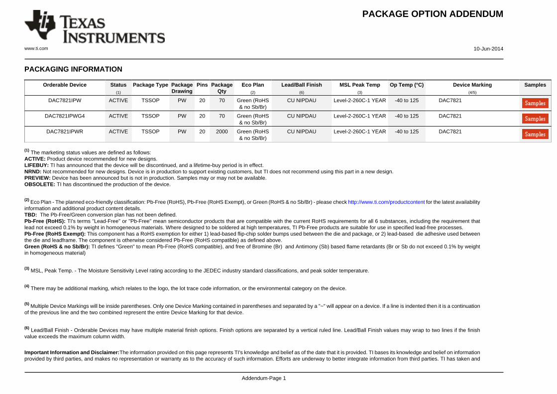
PACKAGING INFORMATION
Orderable Device Status(1)
Package Type PackageDrawing
Pins PackageQty
Eco Plan(2)
Lead/Ball Finish(6)
MSL Peak Temp(3)
Op Temp (°C) Device Marking(4/5)
Samples
DAC7821IPW ACTIVE TSSOP PW 20 70 Green (RoHS& no Sb/Br)
CU NIPDAU Level-2-260C-1 YEAR -40 to 125 DAC7821
DAC7821IPWG4 ACTIVE TSSOP PW 20 70 Green (RoHS& no Sb/Br)
CU NIPDAU Level-2-260C-1 YEAR -40 to 125 DAC7821
DAC7821IPWR ACTIVE TSSOP PW 20 2000 Green (RoHS& no Sb/Br)
CU NIPDAU Level-2-260C-1 YEAR -40 to 125 DAC7821
(1) The marketing status values are defined as follows:ACTIVE: Product device recommended for new designs.LIFEBUY: TI has announced that the device will be discontinued, and a lifetime-buy period is in effect.NRND: Not recommended for new designs. Device is in production to support existing customers, but TI does not recommend using this part in a new design.PREVIEW: Device has been announced but is not in production. Samples may or may not be available.OBSOLETE: TI has discontinued the production of the device.
(2) Eco Plan - The planned eco-friendly classification: Pb-Free (RoHS), Pb-Free (RoHS Exempt), or Green (RoHS & no Sb/Br) - please check http://www.ti.com/productcontent for the latest availabilityinformation and additional product content details.TBD: The Pb-Free/Green conversion plan has not been defined.Pb-Free (RoHS): TI's terms "Lead-Free" or "Pb-Free" mean semiconductor products that are compatible with the current RoHS requirements for all 6 substances, including the requirement thatlead not exceed 0.1% by weight in homogeneous materials. Where designed to be soldered at high temperatures, TI Pb-Free products are suitable for use in specified lead-free processes.Pb-Free (RoHS Exempt): This component has a RoHS exemption for either 1) lead-based flip-chip solder bumps used between the die and package, or 2) lead-based die adhesive used betweenthe die and leadframe. The component is otherwise considered Pb-Free (RoHS compatible) as defined above.Green (RoHS & no Sb/Br): TI defines "Green" to mean Pb-Free (RoHS compatible), and free of Bromine (Br) and Antimony (Sb) based flame retardants (Br or Sb do not exceed 0.1% by weightin homogeneous material)
(3) MSL, Peak Temp. - The Moisture Sensitivity Level rating according to the JEDEC industry standard classifications, and peak solder temperature.
(4) There may be additional marking, which relates to the logo, the lot trace code information, or the environmental category on the device.
(5) Multiple Device Markings will be inside parentheses. Only one Device Marking contained in parentheses and separated by a "~" will appear on a device. If a line is indented then it is a continuationof the previous line and the two combined represent the entire Device Marking for that device.
(6) Lead/Ball Finish - Orderable Devices may have multiple material finish options. Finish options are separated by a vertical ruled line. Lead/Ball Finish values may wrap to two lines if the finishvalue exceeds the maximum column width.
Important Information and Disclaimer:The information provided on this page represents TI's knowledge and belief as of the date that it is provided. TI bases its knowledge and belief on informationprovided by third parties, and makes no representation or warranty as to the accuracy of such information. Efforts are underway to better integrate information from third parties. TI has taken and

PACKAGE OPTION ADDENDUM
www.ti.com 10-Jun-2014
Addendum-Page 2
continues to take reasonable steps to provide representative and accurate information but may not have conducted destructive testing or chemical analysis on incoming materials and chemicals.TI and TI suppliers consider certain information to be proprietary, and thus CAS numbers and other limited information may not be available for release.
In no event shall TI's liability arising out of such information exceed the total purchase price of the TI part(s) at issue in this document sold by TI to Customer on an annual basis.

TAPE AND REEL INFORMATION
*All dimensions are nominal
Device PackageType
PackageDrawing
Pins SPQ ReelDiameter
(mm)
ReelWidth
W1 (mm)
A0(mm)
B0(mm)
K0(mm)
P1(mm)
W(mm)
Pin1Quadrant
DAC7821IPWR TSSOP PW 20 2000 330.0 16.4 6.95 7.1 1.6 8.0 16.0 Q1
PACKAGE MATERIALS INFORMATION
www.ti.com 9-Sep-2014
Pack Materials-Page 1

*All dimensions are nominal
Device Package Type Package Drawing Pins SPQ Length (mm) Width (mm) Height (mm)
DAC7821IPWR TSSOP PW 20 2000 367.0 367.0 38.0
PACKAGE MATERIALS INFORMATION
www.ti.com 9-Sep-2014
Pack Materials-Page 2


IMPORTANT NOTICE
Texas Instruments Incorporated and its subsidiaries (TI) reserve the right to make corrections, enhancements, improvements and otherchanges to its semiconductor products and services per JESD46, latest issue, and to discontinue any product or service per JESD48, latestissue. Buyers should obtain the latest relevant information before placing orders and should verify that such information is current andcomplete. All semiconductor products (also referred to herein as “components”) are sold subject to TI’s terms and conditions of salesupplied at the time of order acknowledgment.TI warrants performance of its components to the specifications applicable at the time of sale, in accordance with the warranty in TI’s termsand conditions of sale of semiconductor products. Testing and other quality control techniques are used to the extent TI deems necessaryto support this warranty. Except where mandated by applicable law, testing of all parameters of each component is not necessarilyperformed.TI assumes no liability for applications assistance or the design of Buyers’ products. Buyers are responsible for their products andapplications using TI components. To minimize the risks associated with Buyers’ products and applications, Buyers should provideadequate design and operating safeguards.TI does not warrant or represent that any license, either express or implied, is granted under any patent right, copyright, mask work right, orother intellectual property right relating to any combination, machine, or process in which TI components or services are used. Informationpublished by TI regarding third-party products or services does not constitute a license to use such products or services or a warranty orendorsement thereof. Use of such information may require a license from a third party under the patents or other intellectual property of thethird party, or a license from TI under the patents or other intellectual property of TI.Reproduction of significant portions of TI information in TI data books or data sheets is permissible only if reproduction is without alterationand is accompanied by all associated warranties, conditions, limitations, and notices. TI is not responsible or liable for such altereddocumentation. Information of third parties may be subject to additional restrictions.Resale of TI components or services with statements different from or beyond the parameters stated by TI for that component or servicevoids all express and any implied warranties for the associated TI component or service and is an unfair and deceptive business practice.TI is not responsible or liable for any such statements.Buyer acknowledges and agrees that it is solely responsible for compliance with all legal, regulatory and safety-related requirementsconcerning its products, and any use of TI components in its applications, notwithstanding any applications-related information or supportthat may be provided by TI. Buyer represents and agrees that it has all the necessary expertise to create and implement safeguards whichanticipate dangerous consequences of failures, monitor failures and their consequences, lessen the likelihood of failures that might causeharm and take appropriate remedial actions. Buyer will fully indemnify TI and its representatives against any damages arising out of the useof any TI components in safety-critical applications.In some cases, TI components may be promoted specifically to facilitate safety-related applications. With such components, TI’s goal is tohelp enable customers to design and create their own end-product solutions that meet applicable functional safety standards andrequirements. Nonetheless, such components are subject to these terms.No TI components are authorized for use in FDA Class III (or similar life-critical medical equipment) unless authorized officers of the partieshave executed a special agreement specifically governing such use.Only those TI components which TI has specifically designated as military grade or “enhanced plastic” are designed and intended for use inmilitary/aerospace applications or environments. Buyer acknowledges and agrees that any military or aerospace use of TI componentswhich have not been so designated is solely at the Buyer's risk, and that Buyer is solely responsible for compliance with all legal andregulatory requirements in connection with such use.TI has specifically designated certain components as meeting ISO/TS16949 requirements, mainly for automotive use. In any case of use ofnon-designated products, TI will not be responsible for any failure to meet ISO/TS16949.
Products ApplicationsAudio www.ti.com/audio Automotive and Transportation www.ti.com/automotiveAmplifiers amplifier.ti.com Communications and Telecom www.ti.com/communicationsData Converters dataconverter.ti.com Computers and Peripherals www.ti.com/computersDLP® Products www.dlp.com Consumer Electronics www.ti.com/consumer-appsDSP dsp.ti.com Energy and Lighting www.ti.com/energyClocks and Timers www.ti.com/clocks Industrial www.ti.com/industrialInterface interface.ti.com Medical www.ti.com/medicalLogic logic.ti.com Security www.ti.com/securityPower Mgmt power.ti.com Space, Avionics and Defense www.ti.com/space-avionics-defenseMicrocontrollers microcontroller.ti.com Video and Imaging www.ti.com/videoRFID www.ti-rfid.comOMAP Applications Processors www.ti.com/omap TI E2E Community e2e.ti.comWireless Connectivity www.ti.com/wirelessconnectivity
Mailing Address: Texas Instruments, Post Office Box 655303, Dallas, Texas 75265Copyright © 2015, Texas Instruments Incorporated
Related Documents