BWW 11 Naturally Commutating Converters The converter circuits considered in this chapter have in common an ac voltage supply input and a dc load output. The function of the converter circuit is to convert the ac source energy into controlled dc load power, mainly for highly inductive loads. Turn-off of converter semiconductor devices is brought about by the ac supply voltage reversal, a process called line commutation or natural commutation. Converter circuits employing only diodes are termed uncontrolled (or rectifiers) while the incorporation of only thyristors results in a (fully) controlled converter. The functional difference is that the diode conducts when forward-biased whereas the turn-on of the forward-biased thyristor can be controlled from its gate. An uncontrolled converter provides a fixed output voltage for a given ac supply and load. Converters employing a combination of both diodes and thyristors are generally termed half-controlled (or semi-controlled). Both fully controlled and half-controlled converters allow an adjustable output voltage by controlling the phase angle at which the forward biased thyristors are turned on. The polarity of the output (load) voltage of a fully controlled converter can reverse (but the current flow direction is not reversible), allowing power flow into the supply, a process called inversion. Thus a fully controlled converter can be described as a bidirectional converter as it facilitates power flow in either direction. The half-controlled converter, as well as the uncontrolled converter, contains diodes which prevent the output voltage from going negative. Such converters only allow power flow from the ac supply to the dc load, termed rectification, and can therefore be described as unidirectional converters. Although all these converter types provide a dc output, they differ in characteristics such as output ripple and mean voltage as well as efficiency and ac supply harmonics. An important converter characteristic is that of pulse number, which is defined as the repetition rate in the direct output voltage during one complete cycle of the input ac supply. A useful way to judge the quality of the required dc output, is by the contribution of its superimposed ac harmonics. The harmonic or ripple factor RF is defined by 2 2 2 2 2 2 1 1 rms dc rms v dc dc V V V RF FF V V − = = − = − where FF is termed the form factor. RF v is a measure of the voltage harmonics in the output voltage while if currents are used in the equation, RF i gives a measure of the current harmonics in the output current. Both FF and RF are applicable to the input and output, and are fully defined in section 11.10. The general analysis in this chapter is concerned with single and three phase ac supplies mainly feeding inductive dc loads. A load dc back emf is used in modelling the dc machine. Generally, uncontrolled rectifier equations can be derived from the corresponding controlled converter circuit equations by setting the controlled delay angle α to zero. Also purely resistive load equations generally can be derived by setting inductance L to zero in the L-R load equations and R-L load equations can be derived from R-L-E equations by setting E, the load back emf, to zero. 11.1 Single-phase uncontrolled converter circuits – ac rectifiers 11.1.1 Half-wave rectifier circuit with an R-L load A simple half-wave diode rectifying circuit is shown in figure 11.1a, while various circuit electrical wave- forms are shown in figure 11.1b. Load current commences when the supply voltage goes positive at ωt = 0. It will be seen that load current flows not only during the positive half of the ac supply voltage, 0 ≤ ωt ≤ π, but also during a portion of the negative supply voltage, π ≤ ωt ≤ β. The load inductor stored energy maintains the load current and the inductor’s terminal voltage reverses and is able to overcome the negative supply and keep the diode forward-biased and conducting. This current continues until all the inductor energy, ½Li 2 , is released (i = 0) at the current extinction angle (or cut-off angle), ωt = β. Naturally commutating converters 222 v L = 0 = Ldi/dt ∴current slope = 0 β R current extinction angle -V R R X = ωL Z = √R 2 +ω 2 L 2 Φ π q =1 r =1 s =1 p = q x r x s p = 1 i During diode conduction the circuit is defined by the Kirchhoff voltage equation = 2 sin (V) R L di L Ri v v v V t dt ω + = + = (11.1) where V is the rms ac supply voltage. Solving equation (11.1) yields the load (and diode) current { } - / tan 2 ( ) sin ( - ) sin e (A) 0 (rad) ω φ ω ω φ φ ω β π = + ≤ ≤ ≥ t V Z i t t t (11.2) Figure 11.1. Half-wave rectifier with an R-L load: (a) circuit diagram and (b) waveforms, illustrating the equal area and zero current slope criteria. where Z = √(R 2 + ω 2 L 2 ) (ohms) tan / cos φ ω φ = = = and L R Q R Z ( ) 0 (A) 2 (rad) i t t ω β ω π = ≤ ≤ (11.3) The current extinction angle β is determined solely by the load impedance Z and can be solved from equation (11.2) when the current, i = 0 with ωt = β, such that β > π, that is

Welcome message from author
This document is posted to help you gain knowledge. Please leave a comment to let me know what you think about it! Share it to your friends and learn new things together.
Transcript

BWW
11 Naturally Commutating Converters The converter circuits considered in this chapter have in common an ac voltage supply input and a dc load output. The function of the converter circuit is to convert the ac source energy into controlled dc load power, mainly for highly inductive loads. Turn-off of converter semiconductor devices is brought about by the ac supply voltage reversal, a process called line commutation or natural commutation. Converter circuits employing only diodes are termed uncontrolled (or rectifiers) while the incorporation of only thyristors results in a (fully) controlled converter. The functional difference is that the diode conducts when forward-biased whereas the turn-on of the forward-biased thyristor can be controlled from its gate. An uncontrolled converter provides a fixed output voltage for a given ac supply and load. Converters employing a combination of both diodes and thyristors are generally termed half-controlled (or semi-controlled). Both fully controlled and half-controlled converters allow an adjustable output voltage by controlling the phase angle at which the forward biased thyristors are turned on. The polarity of the output (load) voltage of a fully controlled converter can reverse (but the current flow direction is not reversible), allowing power flow into the supply, a process called inversion. Thus a fully controlled converter can be described as a bidirectional converter as it facilitates power flow in either direction. The half-controlled converter, as well as the uncontrolled converter, contains diodes which prevent the output voltage from going negative. Such converters only allow power flow from the ac supply to the dc load, termed rectification, and can therefore be described as unidirectional converters. Although all these converter types provide a dc output, they differ in characteristics such as output ripple and mean voltage as well as efficiency and ac supply harmonics. An important converter characteristic is that of pulse number, which is defined as the repetition rate in the direct output voltage during one complete cycle of the input ac supply.
A useful way to judge the quality of the required dc output, is by the contribution of its superimposed ac harmonics. The harmonic or ripple factor RF is defined by
2 2 2
22 2
1 1rms dc rmsv
dc dc
V V VRF FF
V V−
= = − = −
where FF is termed the form factor. RFv is a measure of the voltage harmonics in the output voltage while if currents are used in the equation, RFi gives a measure of the current harmonics in the output current. Both FF and RF are applicable to the input and output, and are fully defined in section 11.10.
The general analysis in this chapter is concerned with single and three phase ac supplies mainly feeding inductive dc loads. A load dc back emf is used in modelling the dc machine. Generally, uncontrolled rectifier equations can be derived from the corresponding controlled converter circuit equations by setting the controlled delay angle α to zero. Also purely resistive load equations generally can be derived by setting inductance L to zero in the L-R load equations and R-L load equations can be derived from R-L-E equations by setting E, the load back emf, to zero. 11.1 Single-phase uncontrolled converter circuits – ac rectifiers 11.1.1 Half-wave rectifier circuit with an R-L load A simple half-wave diode rectifying circuit is shown in figure 11.1a, while various circuit electrical wave-forms are shown in figure 11.1b. Load current commences when the supply voltage goes positive at ωt = 0. It will be seen that load current flows not only during the positive half of the ac supply voltage, 0 ≤ ωt ≤ π, but also during a portion of the negative supply voltage, π ≤ ωt ≤ β. The load inductor stored energy maintains the load current and the inductor’s terminal voltage reverses and is able to overcome the negative supply and keep the diode forward-biased and conducting. This current continues until all the inductor energy, ½Li2, is released (i = 0) at the current extinction angle (or cut-off angle), ωt = β.
Naturally commutating converters 222
vL = 0 = Ldi/dt ∴current slope = 0
β
R
current extinction angle
-VR
R
X = ωL
Z = √R2+ω2L2
Φ
π
q =1 r =1 s =1 p = q x r x s
p = 1
i
During diode conduction the circuit is defined by the Kirchhoff voltage equation
= 2 sin (V)R L
diL Ri v v v V t
dtω+ = + = (11.1)
where V is the rms ac supply voltage. Solving equation (11.1) yields the load (and diode) current
- / tan 2( ) sin ( - ) sin e (A)
0 (rad)
ω φω ω φ φ
ω β π
= +
≤ ≤ ≥
tV
Zi t t
t
(11.2)
Figure 11.1. Half-wave rectifier with an R-L load: (a) circuit diagram and (b) waveforms, illustrating the equal area and zero current slope criteria. where Z = √(R2 + ω2 L2) (ohms)
tan / cosφ ω φ= = =andL R Q R Z
( ) 0 (A)
2 (rad)i t
t
ωβ ω π
=≤ ≤
(11.3)
The current extinction angle β is determined solely by the load impedance Z and can be solved from equation (11.2) when the current, i = 0 with ωt = β, such that β > π, that is
Power Electronics 223
√2/π = 0.45
- / tan sin( - ) sin 0e β φβ φ φ+ = (11.4)
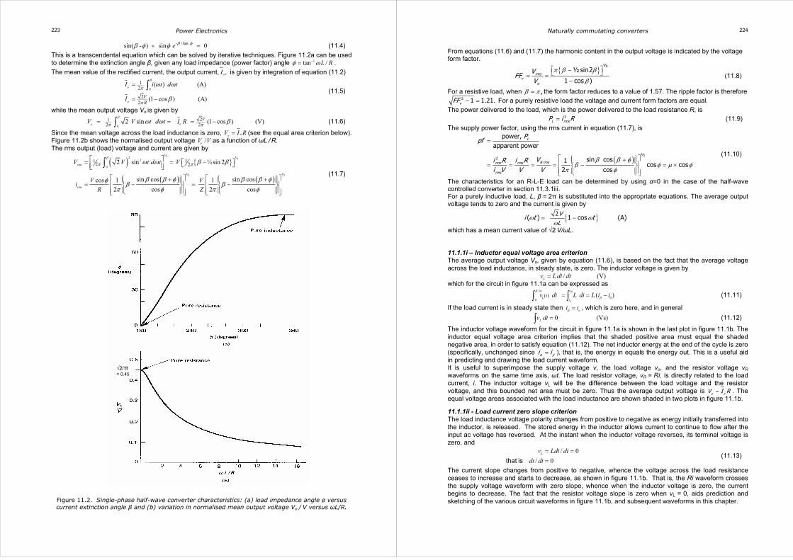
This is a transcendental equation which can be solved by iterative techniques. Figure 11.2a can be used to determine the extinction angle β, given any load impedance (power factor) angle 1tan /L Rφ ω−= .
The mean value of the rectified current, the output current, ,oI is given by integration of equation (11.2)
0
12
22
( ) (A)
(1 cos ) (A)
β
π
π
ω ω
β
=
= −
∫o
oVR
I i t d t
I (11.5)
while the mean output voltage Vo is given by
0
212 2 2 sin (1 cos ) (V)
β
π πω ω β= = = −∫ ooVV V t d t I R (11.6)
Since the mean voltage across the load inductance is zero, = ooV I R (see the equal area criterion below). Figure 11.2b shows the normalised output voltage /oV V as a function of ωL / R. The rms output (load) voltage and current are given by
( )
( ) ( )
2 2
0
½ ½1
2
½ ½
122 sin ½sin 2
sin cos sin coscos 1 12 cos 2 cos
β
π πω ω β β
β β φ β β φφ β βπ φ π φ
= = −
+ + = − = −
∫rms
rms
V V t d t V
V Vi
R Z
(11.7)
Figure 11.2. Single-phase half-wave converter characteristics: (a) load impedance angle ø versus current extinction angle β and (b) variation in normalised mean output voltage Vo / V versus ωL/R.
Naturally commutating converters 224
From equations (11.6) and (11.7) the harmonic content in the output voltage is indicated by the voltage form factor.
½
½sin2
1 cos ) rms
vo
VFF
V
π β β
β
− = =−
(11.8)
For a resistive load, when ,β π= the form factor reduces to a value of 1.57. The ripple factor is therefore 2 1 1.21.vFF − = For a purely resistive load the voltage and current form factors are equal.
The power delivered to the load, which is the power delivered to the load resistance R, is 2
L rmsP i R= (11.9)
The supply power factor, using the rms current in equation (11.7), is
( )2
½
power, apparent power
sin cos1cos cos
2 cos
L
R rmsrms rms
rms
Ppf
Vi R i Ri V V V
β β φβ φ µ φ
π φ
=
+ = = = = − = ×
(11.10)
The characteristics for an R-L-E load can be determined by using α=0 in the case of the half-wave controlled converter in section 11.3.1iii. For a purely inductive load, L, β = 2π is substituted into the appropriate equations. The average output voltage tends to zero and the current is given by
2( ) 1 cos (A)
VL
i t tω
ω ω= −
which has a mean current value of √2 V/ωL. 11.1.1i – Inductor equal voltage area criterion The average output voltage Vo, given by equation (11.6), is based on the fact that the average voltage across the load inductance, in steady state, is zero. The inductor voltage is given by / (V)Lv Ldi dt= which for the circuit in figure 11.1a can be expressed as
/
0 0
( ) ( )o
i
Li
tv dt L di L i iββ ω
β= = −∫ ∫ (11.11)
If the load current is in steady state then oi iβ = , which is zero here, and in general
0 (Vs)Lv dt =∫ (11.12)
The inductor voltage waveform for the circuit in figure 11.1a is shown in the last plot in figure 11.1b. The inductor equal voltage area criterion implies that the shaded positive area must equal the shaded negative area, in order to satisfy equation (11.12). The net inductor energy at the end of the cycle is zero (specifically, unchanged since oi i β= ), that is, the energy in equals the energy out. This is a useful aid in predicting and drawing the load current waveform. It is useful to superimpose the supply voltage v, the load voltage vo, and the resistor voltage vR waveforms on the same time axis, ωt. The load resistor voltage, vR = Ri, is directly related to the load current, i. The inductor voltage vL will be the difference between the load voltage and the resistor voltage, and this bounded net area must be zero. Thus the average output voltage is ooV I R= . The equal voltage areas associated with the load inductance are shown shaded in two plots in figure 11.1b. 11.1.1ii - Load current zero slope criterion The load inductance voltage polarity changes from positive to negative as energy initially transferred into the inductor, is released. The stored energy in the inductor allows current to continue to flow after the input ac voltage has reversed. At the instant when the inductor voltage reverses, its terminal voltage is zero, and
/ 0
/ 0Lv Ldi dt
di dt
= ==that is
(11.13)
The current slope changes from positive to negative, whence the voltage across the load resistance ceases to increase and starts to decrease, as shown in figure 11.1b. That is, the Ri waveform crosses the supply voltage waveform with zero slope, whence when the inductor voltage is zero, the current begins to decrease. The fact that the resistor voltage slope is zero when vL = 0, aids prediction and sketching of the various circuit waveforms in figure 11.1b, and subsequent waveforms in this chapter.
Power Electronics 225
Example 11.1: Half-wave rectifier – constant current In the dc supply half-wave rectifier circuit of figure Example 11.1, the source voltage is 230√2 sin(2π 50t) V with an internal resistance Ri = 1 ohm, RL = 10 ohms, and the filter capacitor C is very large. Calculate
i. the mean value of the load voltage, Vo ii. the diode average and peak currents, ID, DI
∧
iii. the capacitor peak charging and discharging current iv. the diode reverse blocking voltage, VDR
Figure Example 11.1. Single-phase half-wave rectifier: (a) circuit and (b) waveforms. Solution i. Because the load filter capacitor is large, it is assumed that the dc output voltage is ripple free
and constant. The capacitor provides the load current when the ac supply level is less that the dc output. The load current and peak diode (hence supply) current are therefore
2o s o
DoL i
V V VI I
R R
∧ −= =
The ac supply provides current, through the rectifying diode, during the period
( )12 sins s o
i
i V t V tR
ω α ω β= − ≤ ≤
If the capacitor voltage is to be maintained constant, the charge into the capacitor must equal the charge delivered by the capacitor when the diode is not conducting, that is
( )2
s o oi i d t i d tβ α π
α β
ω ω+
− =∫ ∫
Also
2 sin
2 2
o sV V απ θ π θα β
=
− += =
Manipulation yields
1
tan½ ½ 0.110
i
L
RR
θ θ π π πΩ− = = =
Ω
An iterative solution yields θ = 99.6º, that is, the diode conducts for a period of 5.53ms, every cycle of the ac supply. The capacitor voltage is
2 sin 2 sin
2180 99.6
2 230V sin 209.95V2
o s sV V Vπ θα −
= =
° − °= × × =
ii. The average diode current is given by
( )1 1 1
2 sin 2 22 2 2
1 180 99.6 99.62 230V 2 209.95V 21.0A
2 1 2 180
D s o s oi i
i
I V t V d t V cos VR R
cos
β
α
π θω ω θπ π
ππ
− = − = × × − ×
° − ° ° = × × × − × × = Ω °
∫
Vs
Ri D
is
C RL Vo
iC io ωt
ωt
√2Vs
Vo
oπ 2π
α β
DI∧
ID
iD
Vs
θ
Naturally commutating converters 226
Alternatively, as would be expected, the average diode current is
209.95V
21.0A10
oD o
L
VI I
R= = = =
Ω
The peak diode current is
2 2 230V 210V
115.3A1
s oD
i
V VI
R
∧ − × −= = =
Ω
iii. The capacitor peak charging current is the difference between the peak diode current and the
load current, viz., 115A - 21A = 94A, while the peak discharging current is the average load current of 21A.
iv. The diode reverse voltage is the difference between the instantaneous supply voltage and the
output voltage 210V. This is a maximum at the negative peak of the ac supply, when the diode voltage is √2×230V + 210V = 535.3V. During any period when the load is disrupted, the output capacitor can charge to √2×230V, hence the diode can experience, worse case, 2×√2×230V =
650.5V. ♣
11.1.2 Half-wave circuit with an R-L load and freewheel diode
The circuit in figure 11.1a, which has an R-L load, is characterised by discontinuous current (i = 0) and high ripple current. Continuous load current can result when a diode Df is added across the load as shown in figure 11.3a. This freewheel diode prevents the voltage across the load from reversing during the negative half-cycle of the ac supply voltage. The inductor energy is not returned to the ac supply, rather is retained in the load circuit. The stored energy in the inductor cannot reduce to zero instantaneously, so the current is forced to find an alternative path whilst decreasing towards zero. When the rectifier diode D1 ceases to conduct at zero volts it blocks, and diode Df provides an alternative load current freewheeling path, as indicated by the waveforms in figure 11.3b. The output voltage is the positive half of the sinusoidal input voltage. The mean output voltage (thence mean output current) is
0
12
2
2
sin
0.45 (V)
π
π
π
ω ω= =
= = × =
∫oo
oo
V
V I R V t d t
V V I R (11.14)
The rms value of the load circuit voltage v0 is given by
( )
2 π
0
12 2 sin
0.71 (V)2
π ω ω=
= = ×
∫rms
V
V V t d t
V (11.15)
The output ripple (ac) voltage is defined as
2 2
2 22 2
2 0.545π
−
= − = ×
Ri rms o
V V
V V V
V (11.16)
hence the load voltage form and ripple factors are defined as
( )2
2 2
/ / 1
½ 1.57 1 ¼ 1 1.211π π
= = −
= = = − = − =
rms
v rms o v Ri o o
v
V
VFF V V RF V V
FF (11.17)
After a large number of ac supply cycles, steady-state load current conditions are established, and from Kirchhoff’s voltage law, the load current is defined by
2 sin (A) 0diL Ri V t t
dtω ω π+ = ≤ ≤ (11.18)
and when the freewheel diode conducts
0 (A) 2diL Ri t
dtπ ω π+ = ≤ ≤ (11.19)

Power Electronics 227
q =1 r =1 s =1 p = q x r x s
p = 1
Figure 11.3. Half-wave rectifier with a load freewheel diode and an R-L load: (a) circuit diagram and parameters and (b) circuit waveforms.
During the period 0 ≤ ωt ≤ π, when the freewheel diode current is given by iDf = 0, the supply current, which is the load current, are given by
2/ tan( ) ( ) 2 2sin( ) ( sin ) (A)
0o o
tt t
V Vi i t I eZ Zt
πω φω ω ω φ φ
ω π
−= = − + +
≤ ≤ (11.20)
for
2
/ tan
/ tan / tan2 1sin (A)π
π φ
π φ π φφ−
−
+=
−o
V eI
Z e e
2 2 ( ) (ohms)
tan /Z R L
L R
ωφ ω
= +
=
where
During the period π ≤ ωt ≤ 2π, when the supply current i = 0, the freewheel diode current and hence load current are given by 1
( ) / tan( ) ( ) (A) 2o Df o
tt ti i I e tπ
ω π φω ω π ω π− −= = ≤ ≤ (11.21)
for / tan
1 2 (A)o oI I eπ φπ π=
For discontinuous load current (the freewheel diode current iDf falls to zero before the rectifying diode D1 recommences conduction), the appropriate integration gives the average diode currents as
Naturally commutating converters 228
( )( )
( )
/ tan 21
/ tan 21
2 1 sin2
1 sin2
π φ
π φ
φπ
φπ
−
−
= − + ×
= − = + ×
D
Df o D
VI e
R
VI I I e
R
(11.22)
In figure 11.3b it will be seen that although the load current can be continuous, the supply current is discontinuous and therefore has a high harmonic content. The output voltage Fourier series (Vo + V1 + Vn = 2, 4, 6..) is
( ) ( ). . .
2 2,4,6
2 2 2 2sin cos2 1
ω ωπ π
∞
== + −
−∑on
V V Vv t t n t
n (11.23)
Dividing each harmonic output voltage component by the corresponding load impedance at that frequency gives the harmonic output current, whence rms current. That is
( )22
n n nn
n
V V VI
Z R jn L R n Lω ω= = =
+ + (11.24)
and
2 2
1, 2, 4, 6..
½=
= + ∑rms o nn
I I I (11.25)
Example 11.2: Half-wave rectifier In the circuit of figure 11.3, the source voltage is 240√2 sin(2π 50t) V, R = 10 ohms, and L = 50 mH. Calculate
i. the mean and rms values of the load voltage, Vo and Vrms ii. the mean value of the load current, oI iii. the current boundary conditions, namely Io1π and Io2π iv. the average freewheel diode current, hence average rectifier diode current v. the rms load current, hence load power and supply rms current vi. the supply power factor
If the freewheel diode is removed from across the load, determine vii. an expression for the current hence the current extinction angle viii. the average load voltage hence average load current ix. the rms load voltage and current x. the power delivered to the load and supply power factor
From the rms and average output voltages and currents, determine the load form and ripple factors. Solution i. From equation (11.14), the mean output voltage is given by
2 2 240V 108Vπ π×= = =o
VV
From equation (11.15) the load rms voltage is
/ 2 240V / 2 169.7V= = =rmsV V
ii. The mean output current, equation (11.5), is
2 2×240V= = 10.8Aπ×10π= = Ωo
o
V VI R R
iii. The load impedance is characterised by
2 2
2 2
( )
10 (2 50Hz 0.05) 18.62tan /
2 50Hz 0.05H /10 1.57 or 57.5 1rad
ω
πφ ω
π φ
= +
= + × × = Ω
== × × Ω = = ° ≡
Z R L
L R
From section 11.1.2, equation (11.20)

Power Electronics 229
2
12
/ tan
/ tan / tan
/1.57
/1.57 /1.57
2 1sin
12 240V sin(tan 1.57) = 3.41A18.62
π
π
π φ
π φ π φ
π
π π
φ
−
−
−
−
−
+=
−+×= × ×Ω −
o
o
eVI Z e e
eI
e e
Hence, from equation (11.21) 1 2
/ tan /1.573.41 = 25.22Ao oI I e eπ ππ φ π= = ×
Since 2 3.41A 0π = >oI , continuous load current flows.
iv. Integration of the diode current given in equation (11.21) yields the average freewheel diode current.
1
0 0
1.57
0
/ tan
/1.57rad
( )1 1
2 2
1 25.22A25.22A 1.57rad 1 5.46A2 2
Df Df o
t
t
tI i d t I e d t
e d t e
π π
π
π π
ω φ
ω
ω ω ωπ π
ωπ π
−
−
−
= =
= × = × × − =
∫ ∫
∫
The average input current, which is the rectifying diode mean current, is given by
1 10.8A 5.46A 5.34A= = − = − =Dfs D oI I I I v. The load voltage harmonics given by equation (11.24) can be used to evaluate the load current at
the load impedance for that frequency harmonic.
( ) ( ) ( ). . .
2 2,4,6
2 2 2 2sin cos2 1
ω ωπ π
∞
== + −
−∑n
V V Vv t t n t
n
The following table shows the calculations for each frequency component.
harmonic n
( ).
2
2 21 π
=−n
VV
n(V)
( )22 ω= +nZ R n L
(Ω)
= nn
n
VI
Z(A)
2½ nI
0 (108.04) 10.00 10.80 (116.72)
1 (169.71) 18.62 9.11 41.53
2 72.03 32.97 2.18 2.39
4 14.41 63.62 0.23 0.03
6 6.17 94.78 0.07 0.00
8 3.43 126.06 0.03 0.00
2 2½o nI I+ =∑ 160.67
The rms load current is
.
2 2
1, 2, 4..
½ 160.7 12.68A=
= + = =∑rms o nn
I I I
The power dissipated in the load resistance is therefore 2 2
10 12.68A 10 1606.7WrmsP I RΩ = = × Ω =
The freewheel diode rms current is
( )
( )
.
.
2
10
2
0
( ) / tan
( ) /1.57rad
121 25.22A 8.83A
2
π
π
π
ω φ
ω
ωπ
ωπ
−
−
=
= × =
∫
∫
Df o
t
t
I I e d t
e d t
Thus the input (and rectifying diode) rms current is given by
2 2
1
2 212.68 8.83 9.09A= = −
= − =rms rmsD s rms Df rmsI I I I
vi. The input ac supply power factor is
1606.7W 0.74
240V 9.09A= = =
×out
rms rms
Ppf
V I
Naturally commutating converters 230
vii. If the freewheel diode Df is removed, the current is given by equation (11.2), that is
- / tan
- /1.57
- /1.57
2
2 V18.62
( ) sin ( - ) sin e
240 = sin ( -1.0) 0.841 e
= 18.23 sin ( -1.0) 0.841 e (A) 0 (rad)
ω φ
ω
ω
ω ω φ φ
ω
ω ω βΩ
= +
×+ ×
× + × ≤ ≤
t
t
t
V
Zi t t
t
t t
The current extinction angle β is found by setting i = 0 and solving iteratively for β. Figure 11.2a gives an initial estimate of 240° (4.19 rad) when φ = 57.5° (1 rad). That is
- /1.570 = sin ( -1.0) 0.841 e ββ + ×
gives β = 4.08 rad or 233.8°, after iteration.
viii. The average load voltage from equation (11.6) is
2 2 240V2 2 (1 cos ) (1 cos 4.08) 86.0Vπ πβ ×= − = − =o
VV
The average load current is
/ = 86.0V/10 = 8.60A= ΩooI V R
ix. The load rms voltage is 169.7V with the freewheel diode and increases without the diode to, as
given by equation (11.7),
½
½
12
12
½ sin 2
240V 4.08 ½sin 2 4.08 181.6V
π
π
β β = −
= − × =
rmsV V
The rms load current from equation (11.7) is decreased to
( )
( )
½
½
sin cos12 cos
sin 4.08cos 4.08 1.57240V 1 4.08 9.68A18.62 2 cos1.57
β α β φβ
π φ
π
+ + = −
+ = × − = Ω
rms
Vi
Z
Removal of the freewheel diode decreases the rms load current from 12.68A to 9.68A. x. The load power is reduced without a load freewheel diode, from 1606.7W with a load freewheel
diode, to 2 2
10 9.68 10 937WΩ = = × Ω =rmsP i R
The supply power factor is also reduced, from 0.74 to
937W 0.40
240V 9.68A= = =
×out
rms rms
Ppf
V I
circuit with freewheel diode circuit without freewheel diode
Load factor form factor ripple factor form factor ripple factor
FF = rms/ave RF = √FF2-1 FF = rms/ave RF = √FF2-1
Voltage factor 169.7V/108V = 1.57 1.21 181.6V/86V = 2.1 1.86
Current factor 12.68A/10.8A = 1.17 0.615 9.68A/8.60A = 1.12 0.517
♣
11.1.3 Single-phase, full-wave bridge rectifier circuit Single-phase uncontrolled full-wave bridge circuits are shown in figures 11.4a and 11.4b. Both circuits appear identical as far as the load and supply are concerned. It will be seen in part b that two fewer diodes can be employed but this circuit requires a centre-tapped secondary transformer where each secondary has only a 50% copper utilisation factor. For the same output voltage, each of the secondary windings in figure 11.4b must have the same rms voltage rating as the single secondary winding of the transformer in figure 11.4a. The rectifying diodes in figure 11.4b experience twice the reverse voltage, (2√2 V), as that experienced by each of the four diodes in the circuit of figure 11.4a, (√2 V).

Power Electronics 231
q =2 r =1 s =1 p = q x r x s
p = 2
Figure 11.4c shows bridge circuit voltage and current waveforms. With an inductive passive load, (no back emf) continuous load current flows, which is given by
( ) ( ) / tan/ tan
2 2sinsin 01
ω φπ φ
φω ω φ ω π−
−
= − + × ≤ ≤ − t
o
Vi t t e t
Z e (11.26)
Appropriate integration of the load current squared, gives the rms load (and ac supply) current:
( )2 / tan½
1 4sin tan 1 π φφ φ − = + × + = rms s
VI e I
Z (11.27)
The load experiences the transformer secondary rectified voltage which has a mean voltage (thence mean load current) of
0
12 22sin 0.90 (V)
π
π πω ω= = = =∫ oo
VV V t d t I R V (11.28)
Since the average inductor voltage is zero, the average resistor voltage equals the average R-L voltage. The rms value of the load circuit voltage v0 is
( )2 2π
0
12 2 sin (V)π ω ω= =∫rmsV V t d t V (11.29)
Figure 11.4. Single-phase full-wave rectifier bridge: (a) circuit with four rectifying diodes; (b) circuit with two rectifying diodes; and (c) circuit waveforms.
Naturally commutating converters 232
From the load voltage definitions in section 11.10, the load voltage form factor is
1.112 2
π
= = =rmsv
o
V VFF
V V (11.30)
The load ripple voltage is
( )
2 2
22 22 2= = 0.435 (V)
RI rms oV V V
V V Vπ
−
− (11.31)
hence the load voltage ripple factor is
( )
2
22 2 2
/ 1
21 0.483/π π
= −
= − =
v RI o v
v
RF V V FF
RF (11.32)
which is significantly less (better) than the half-wave rectified value of 1.211 from equation (11.17).
The output voltages and currents (rms and average) can be derived from the voltage Fourier expansion form for a half-sine wave:
( ) 22,4,6
2 2 2 2 2 cos1
ω ωπ π
∞
== +
−∑on
V Vv t n t
n (11.33)
The first term is the average output voltage, as given by equation (11.28). Note the harmonic
magnitudes decrease rapidly with increased order, namely 2 2 2 2: : : : ...153 35 63 The output voltage is
therefore dominated by the dc component and the harmonic at 2ω. The output current can be derived by dividing each voltage component by the appropriate load impedance at that frequency. That is
( )
2
22
2 2
22 2 1 2, 4,6..
π
π ω
= =
−= = × =+
for
oo
nn
n
V VI
R R
V V nI nZ R n L
(11.34)
The load rms current whence load power, critical load inductance, and power factor, are given by
2 2 2
2,4½
( )3 ω
∞
== + × =
= = =×
∑
see equation 11.38
rms o n L rms
rmsLcritical
rms
nI I I P I R
I RP Rpf L
V I V
(11.35)
Each diode rms current is / 2rmsI . For the circuit in figure 11.4a, the transformer secondary winding rms current is Irms, while for the centre-tapped transformer, for the same load voltage, each winding has an rms current rating of Irms / √2. The primary current rating is the same for both transformers and is related to the secondary rms current rating by the turns ratio. 11.1.3i - Single-phase full-wave bridge rectifier circuit with an output L-C filter
A – with an output L-C filter and continuous load current Table 11.1 shows three typical single-phase, full-wave rectifier output stages, where part c is a typical output filtering stage used to obtain a near constant dc output voltage. If it is assumed that the load inductance is large and the load resistance small such that continuous load current flows, then the bridge average output voltage oV is the same as the average voltage across the load resistor since the average voltage across the filter inductor is zero. From equation (11.33), the dominant load voltage harmonic is due to the second harmonic therefore the ac current is predominately the second harmonic current, , , 2≈o ac oI I . By neglecting the higher order harmonics, the various circuit currents and voltages can be readily obtained as shown in table 11.1. From equation (11.33) the output voltage is given by
Power Electronics 233
( ) , 2
2
cos 22 2 2 2 2 cos 212 2 2 2 2 cos 230.90 0.60 cos 2
ω ω
ωπ π
ωπ πω
= +
= + × =−
= + ×
= + ×
o oov t V V t
V Vn t n
nV V
t
V V t
for (11.36)
With the filter capacitor across the load resistor, the average inductor current is equal to the average resistor current, since the average capacitor current is zero. With continuous inductor current, the inductor current is
( )
( )
, 2
222
cos 22 0.90 0.60cos 2 cos 23 2
ω ω
ω ωω
= +
= + = + ×+
oo o
o o
i t I I t
V V V Vt t
R Z R R L
(11.37)
From equation (11.37) for continuous inductor current, the average current must be larger than the peak second harmonic current magnitude, that is
, 2
2
23
>
>
o o
o o
I I
V V
R Z
(11.38)
Table 11.1. Single-phase full-wave uncontrolled rectifier circuits – continuous inductor current
2nd harmonic current
average output current
output power
Io,2 oI PR+PE
Full-wave rectifier circuit
Load circuit (A) (A) (W)
(a)
R-L
see section 11.1.3
and 11.3.3 α = 0
( ),2
22 2ω+
oV
R L
2 2π
=
oV
R
V
R
2, o rmsI R
(b)
R-L-E
see section 11.3.4 α = 0
( ),2
22 2ω+
oV
R L
1 2 2π
−
= −
oV E
R
VE
R
2, + oo rmsI R I E
(c)
L-R//C
see section 11.1.3i
,2
2ωoV
L
2 2π
=
oV
R
V
R
22
, = oo rmsII R R
Vs Is
Io
Vo
Io,dc
Io,ac
L
C R
Vs Is
Io
Vo E +
L
R
Vs
Is
Io
Vo
L
R
Naturally commutating converters 234
Since the load resistor must be small enough to ensure continuous inductor current, then 2ω >L R such that ( )22
2 22 ωω= ≈+Z LR L . Equation (11.38) therefore gives the following load identity for continuous inductor current
2
1 2 1 1 133 3 ωω
> = >LRR Z L
that is (11.39)
The load and supply (peak) ac currents are , , , 2= =o ac s ac oI I I . The output and supply rms currents are
2 22 2
, , , , 2½ ½= = + = +o oo rms s rms o ac oI I I II I (11.40)
and the power delivered to resistance R in the load is 2
,=R o rmsP I R (11.41)
B – with an output L-C filter and discontinuous load current
If the inductor current reduces to zero, at angle β, all the load current is provided by the capacitor. Its voltage falls to Vo (<√2 V) and inductor current recommences when
2 sinL ov V t Vω= − (11.42)
at an angle
1sin2
oV
Vα −= (11.43)
By integrating v = L di/dt for i, the inductor current is of the form
( ) ( ) ( )( )12 cos cosL oi t V t V t
Lω α ω ω α
ω= − − − (11.44)
where α ≤ ωt ≤ β. The voltage Vo is found from equation (11.44) by iterative techniques. Example 11.3: Full-wave uncontrolled rectifier with an L-C filter and continuous load current A single-phase, full-wave, diode rectifier is supplied from a 230V ac, 50Hz voltage source and uses an L-C output filter with a resistor load, as shown in the last circuit in Table 11.1. The average inductor current is 10A with a 4A rms ripple current dominated by the 100Hz component. Ignoring diode voltage drops and initially assuming the output voltage is ripple free, determine
i. the dc output voltage, hence load resistance and power ii. the dc filter inductance and its average voltage, whilst neglecting any capacitor voltage ripple iii. the dc filter capacitance if its peak-to-peak ripple voltage is 5% the average voltage iv. diode average, rms, and peak current v. the supply power factor
Solution
Since ( ), 22 2 4A 10A< × <o rms oI I , the output current is continuous.
i. The dc output voltage is oV = 0.9×230V = 207V. Assuming the 207V is ripple free, that is, Vrms = Vdc, then the load resistance and power dissipated are
207V 20.710A
207V 10A = 2070W
= = = Ω
= × = ×
o
o
R oo
VR
I
P V I
ii. The 100Hz voltage component in the output voltage is given by equation (11.36), that is
, 2 2
2 2 2 cos1
2 2 2 cos 230.60 230V cos 2 138 cos 2
ωπ
ωπω ω
= ×−
= ×
= × × = ×
o
VV n t
nV
t
t t
which has an rms value of 138/√2 = 97.6V. The 100Hz rms current , 2 / 2oI produced by this voltage is 4A thus

Power Electronics 235
, 2 , 2
, 2
, 2
2297.6V 38.8mH
2 2 2 50Hz 4A
ω
ω π
=
= = =× ×
from o o
o
o
I V
L
VL
I
The average inductor voltage is zero. iii. From part i, the dc output voltage is 207V. The peak-to-peak ripple voltage is 5% of 207V, that is
10.35V. This gives an rms value of 10.35V /2√2 = 3.66V. From
, 2
, 2 , 2, 100Hz
, 2
, 2
22 2 2
4A 1.7mF2 2 2 50Hz 3.66V
ω
ω π
= × =
⇒ = = =× × ×
o
o oc
o
o
IV I
XC
IC
V
iv. The diode currents are
2 2 2 2, , , 2
, 2
/ 2 ½ / 2 10A 4A / 2 10.8A / 2 7.64A
/ 2 = 10A/2 = 5A
10A 2 4A 15.7A
= = + = + = =
=
= + = + × =
D rms o rms oo
D o
D o o
I I II
I I
I II
v. The input and output rms current is
2 2 2 2
, , 2½ 10A 4A 10.8A= = + = + =s o rms ooI I II
Assuming the input power equals the output power, then from part i, Po = Pi = 2070W. The supply power factor is
2070W 0.83
230V 10.8A= = = =
×i i
s s
P Ppf
S V I
♣ 11.1.3ii - Single-phase full-wave bridge circuit with highly inductive load – constant load current
With a highly inductive load, which is the usual practical case, virtually constant load current flows, as shown dashed in figure 11.4c. The bridge diode currents are then square wave 180º blocks of current of magnitude oI . The diode current ratings can now be specified and depend on the pulse number p. For this full-wave single-phase application each input cycle comprises two 180º output current pulses, hence p = 2. The mean current in each diode is
1 ½ (A)= =D o opI I I (11.45)
and the rms current in each diode is
1 2/ (A)= =o oD pI I I (11.46)
whence the diode current form factor is
2/= = =DID DRF I I p (11.47)
Since the load current is approximately constant, power delivered to the load is
228 (W)
π×≈ =o o o
V RP V I (11.48)
The supply power factor is pf = /o
V V = 2√2/π = 0.90, since o rmsI I= .
11.1.3iii - Single-phase full-wave bridge rectifier circuit with a C-filter and resistive load
The capacitor smoothed single-phase diode rectifier circuit shown in figure 11.5a is a common power rectifier circuit used to obtain unregulated dc voltages. The circuit is simple and cheap but the input current has high peak and rms values, high harmonics, and a poor power factor. The capacitor reduces the ripple voltage, so large voltage-polarised capacitance is used to produce an almost constant dc output voltage. Isolation and voltage matching (step-up or step down) are obtained by using a transformer before the diode rectification stage as shown in figures 11.4a and b. The resistor R across the filter capacitor represents a resistive dissipative load.
Naturally commutating converters 236
As the ac supply voltage rises to its extremes each half cycle, as shown in figure 11.5b, a pair of rectifier diodes D1-D2 or D3-D4, alternately become forward biased at time ωt = α. The ac supply provides load resistor current and simultaneously charges the capacitor, its voltage having drooped whilst providing the load current during the previous diode non-conduction period. The capacitor charging current period θc around the ac supply extremes is short, giving a high peak to rms ratio of diode and supply current. When all the rectifier diodes are reverse biased at ωt = β because the capacitor voltage is greater than the instantaneous supply ac voltage, the capacitor supplies the load current and its voltage decreases with an R-C time constant until ωt = π+α. The output voltage and diode voltages, plus load current vo /R, and capacitor current C dvo /dt are defined in Table 11.2. The start of diode conduction, α, the diode current extinction angle, β, hence diode conduction period, θc, are specified by the following equations. From ic + iR = 0 at ωt = β :
( ) ( )1 1
2 2cos sin 0
tan tan ½
β β
β ω π ω π β π− −
+ =
= − = − ≤ ≤
V V
X RRC RC
(11.49)
By equating the two expression for output voltage at the boundary ωt = π+α gives
( ) ( ) / tan2 sin 2 sin π α β βπ α β − + −+ = ×V V e (11.50)
and a transcendental expression for α results:
( ) /sin sin 0π α β ωα β − + −− × =RCe (11.51)
Figure 11.5. Single-phase full-wave rectifier bridge: (a) circuit with C-filter capacitor and (b) circuit waveforms.
(a)
(b)
iR
α β
ωt
½π 2π π + α o
Vs
π
ICap
α β π + α
θc
ωt
∆vo
vo √2 V
D1 D3
D1 D3
D2 D4
D2 D4
conducting diodes
θc
vo
D4 D1
D3 D2
Vs C R
ic iR
vo
iD
is
iD
ov∨
−
Power Electronics 237
Table 11.2. Single-phase, full-wave rectifier voltages and currents
Diodes conducting Diodes non-conducting vs(ωt) = √2Vsinωt
α ≤ ωt ≤ β β ≤ ωt ≤ π + α
Output voltage vo(ωt) 2 sinωV t ( ) / tan2 sin ω β ββ − −× tV e
Diode voltage vD(ωt) 0 - 2 sinωV tand ( ) / tan2 sin 2 sinω β ββ ω− −− × +tV e V t
Capacitor current ic(ωt) 2 cosωVt
X ( ) / tan2 ω β β− −× tV
eZ
Resistor current iR(ωt) 2 sinωVt
R ( ) ( )/ tan2 ω β β ω− −× = −t
c
Ve i t
Z
Diode bridge current ID(ωt)=
ic(ωt)+ iR(ωt) ( )2 sin
cosω φ
φ× +
Vt
R 0
The diode current conduction period θc is given by θ β α= −c (11.52)
When the diodes conduct, R and C are in parallel and tanφ ω= C R .
When the diodes are not conducting, the output circuit current flows in a series R-C circuit with a fundamental impedance of:
2 2 1 ω= + =Z R X X Cand
The resistor average voltage and current are
( )1 cos2
cosθ
π β−
= =−
cR R
VV I R (11.53)
The maximum output voltage occurs at ωt = ½π when vo = = soV V =√2V, while the minimum output voltage occurs at the end of the capacitor discharge period when ωt = α and vo =
∨
oV =√2Vsinα. The output peak-to-peak ripple voltage is therefore the difference:
( )2 2 sin 2 1 sinα α∨
∆ = − = − = −oooV V V V V V (11.54)
By assuming α ≈ ½π, β ≈ ½π, and a series expansion for the exponent
2
2π
ω∆ ≈ =o
V VV
RC f RC (11.55)
The ac source current is the sum of the diode currents, that is 1,2 3,4= − = +s D D R ci i i i i (11.56)
when α ω β< <t . Otherwise is = 0.
Since the capacitor voltage is in steady-state, the average capacitor current is zero, thus for full-wave rectification, the average diode current is half the average load current. The peak capacitor current occurs at ωt = α, when the diodes first conduct. From the capacitor current equation in table 11.2:
2 cosω α=cI V C (11.57)
From table 11.2, the peak diode current occurs at the same time as the peak capacitor current, ωt = α:
( ) ( )
( )2 2 2 22 cos sin cos sin sin
π α π α
ω α α α α α φ
= + + +
= + = + = +
D c RI i i
V V V V ZV C
R X R R X
(11.58)
Similar expressions can be derived for the half-wave rectifier case. For the non-conduction period, β=2π+α. The output ripple voltage is about twice that given by equation (11.55) and the average resistor voltage in equation (11.53) (after modification), is reduced. Example 11.4: Single-phase full-wave bridge rectifier circuit with C-filter and resistive load A single-phase, full-wave, diode rectifier is supplied from a 230V ac, 50Hz voltage source and uses a capacitor output filter, 1000µF, with a resistor 100Ω load, as shown in Figure 11.5a. Ignoring diode voltage drops, determine
Naturally commutating converters 238
i. expressions for the output voltage ii. output voltage ripple ∆vo and the % error in using the approximation equation (11.55) iii. expressions for the capacitor current iv. diode peak current v. the average load voltage and current
Assuming the output ripple voltage is triangular, estimate vi. the average output voltage and rms output ripple voltage vii. capacitance C for ∆vo = 2% of the maximum output voltage
Solution
The supply voltage is vs = √2×230 sin2π 50t, which has a peak value of sV = 325.3V.
2 50Hz 100 1000µF = 31.416 radω π= × Ω×RC
Thus X = 1/ωC = 3.1831Ω and Z = 100.0507Ω. From equation (11.49) the diode current extinction angle β is ( ) ( )1 1tan tan 31.416rad 1.6026 rad 91.8β π ω π− −= − = − = = °RC
The diode current turn-on angle α is solve iteratively from equation (11.51), that is
( )
( )
/
1.603 / 31.416
sin sin 0
sin sin1.603 0
π α β ω
π α
α β
α
− + −
− + −
− × =
− × =
RCe
e
gives α = 1.16095 rad or 66.5°. The diode conduction period is θc = β - α =1.6026 -1.16095 = 0.44167rad or 25.3°. i. From table 11.2, the output voltage, which is the capacitor voltage, is given by
( ) ( )1.6026rad /31.416rad 1.6026rad /31.416rad
( ) 2 sin 325.27V sin
66.5 91.8
( ) 2 230V sin1.6026rad 325.1391.8 246.5
ω ω
ω ω ω
ω
ωω
− − − −
= = ×
° ≤ ≤ °
= × × × = ×° ≤ ≤ °
o
o
t t
v t V t t
t
v t e e
t
ii. The output voltage ripple ∆vo is given by equation (11.54), that is
( ) ( )2 1 sin 2 230V 1 sin1.16026 26.94V p-pα∆ = − = × − =oV V
From equation (11.55)
. .
230V 32.5V2 2 50Hz 100 1000µF
∆ ≈ = =× × Ω×
o
VV
f RC
The approximation predicts a higher ripple: a +21% over-estimate.
iii. From table 11.2, the capacitor current is
( ) ( ) ( )/ 1.16 / 31.4 1.16 / 31.4
( ) 2 cos 2 230V 2 50Hz 1000µF cos 102.2 cos66.5 91.8
2 sin 2230V sin1.16( ) 3.0100
91.8 246.5
ω β ω ω ω
ω ω ω π ω ωω
βω
ω
− − − − − −
= = × × × = ×° ≤ ≤ °
×= × = × = ×
Ω° ≤ ≤ °
c
c
t RC t t
i t V C t t t
t
Vi t e e e
Rt
iv. The peak diode current is given by equation (11.58):
22 cos sin
2 230V2 230V 2 50Hz 1000µF cos1.16026 sin1.16026100
40.7A 3A 43.7A
ω α α
π
= +
= × × × + ×Ω
= + =
D
VI V C
R
The peak diode current is dominated by the capacitor initial charging current of 40.7A
Power Electronics 239
v. The average load voltage and current are given by equation (11.53)
( )
( )
1 cos2cos
1 cos 0.44172 230V 312.3Vcos1.603
312.3V 3.12A100
θπ β
π
−=
−
−= × =
−
= = =Ω
cR
R
R
VV
VI
R
vi. If the ripple voltage is assumed triangular then
(a) The average output voltage is the peak output voltage minus half the ripple voltage, that is
sV - ½∆vo = √2×230V - ½×26.9V = 311.8V
which is less than that given by the accurate equation (11.54), 312.3V. (b) If the 26.9V p-p ripple voltage is assumed triangular then its rms value is ½×26.9/√3 =7.8V rms.
vii. Re-arrangement of equation (11.55), which under-estimates the capacitance requirement for
2% ripple, gives
.
12 2%2 2 2%of
1 5,000µF2 50Hz 100 0.02
= = =××∆ ×
= =× × Ω×
s
o s
VVC
f Rf R V f R V
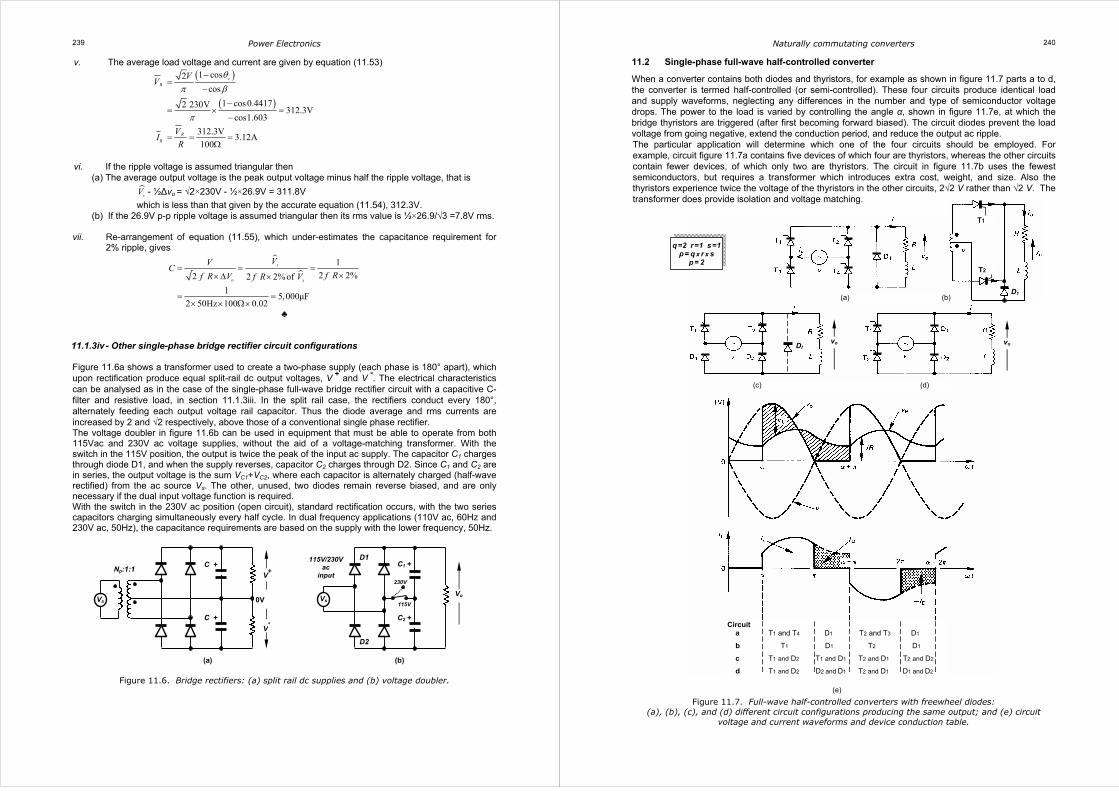
♣ 11.1.3iv - Other single-phase bridge rectifier circuit configurations Figure 11.6a shows a transformer used to create a two-phase supply (each phase is 180° apart), which upon rectification produce equal split-rail dc output voltages, V + and V -. The electrical characteristics can be analysed as in the case of the single-phase full-wave bridge rectifier circuit with a capacitive C-filter and resistive load, in section 11.1.3iii. In the split rail case, the rectifiers conduct every 180°, alternately feeding each output voltage rail capacitor. Thus the diode average and rms currents are increased by 2 and √2 respectively, above those of a conventional single phase rectifier. The voltage doubler in figure 11.6b can be used in equipment that must be able to operate from both 115Vac and 230V ac voltage supplies, without the aid of a voltage-matching transformer. With the switch in the 115V position, the output is twice the peak of the input ac supply. The capacitor C1 charges through diode D1, and when the supply reverses, capacitor C2 charges through D2. Since C1 and C2 are in series, the output voltage is the sum VC1+VC2, where each capacitor is alternately charged (half-wave rectified) from the ac source Vs. The other, unused, two diodes remain reverse biased, and are only necessary if the dual input voltage function is required. With the switch in the 230V ac position (open circuit), standard rectification occurs, with the two series capacitors charging simultaneously every half cycle. In dual frequency applications (110V ac, 60Hz and 230V ac, 50Hz), the capacitance requirements are based on the supply with the lower frequency, 50Hz.
Figure 11.6. Bridge rectifiers: (a) split rail dc supplies and (b) voltage doubler.
(a) (b)
V+
C +
V-
C +
Np:1:1
Vs
230V
C1 +
Vo
C2 +
115V/230Vac
input
Vs 115V
D1 D2
0V
Naturally commutating converters 240
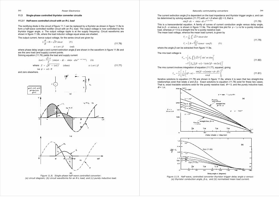
11.2 Single-phase full-wave half-controlled converter
When a converter contains both diodes and thyristors, for example as shown in figure 11.7 parts a to d, the converter is termed half-controlled (or semi-controlled). These four circuits produce identical load and supply waveforms, neglecting any differences in the number and type of semiconductor voltage drops. The power to the load is varied by controlling the angle α, shown in figure 11.7e, at which the bridge thyristors are triggered (after first becoming forward biased). The circuit diodes prevent the load voltage from going negative, extend the conduction period, and reduce the output ac ripple. The particular application will determine which one of the four circuits should be employed. For example, circuit figure 11.7a contains five devices of which four are thyristors, whereas the other circuits contain fewer devices, of which only two are thyristors. The circuit in figure 11.7b uses the fewest semiconductors, but requires a transformer which introduces extra cost, weight, and size. Also the thyristors experience twice the voltage of the thyristors in the other circuits, 2√2 V rather than √2 V. The transformer does provide isolation and voltage matching.
Figure 11.7. Full-wave half-controlled converters with freewheel diodes: (a), (b), (c), and (d) different circuit configurations producing the same output; and (e) circuit
voltage and current waveforms and device conduction table.
(e)
(a) (b)
(c) (d)
Df
D1
T1
T2
Circuit a T1 and T4 D1 T2 and T3 D1
b T1 D1 T2 D1
c T1 and D2 T1 and D1 T2 and D1 T2 and D2
d T1 and D2 D2 and D1 T2 and D1 D1 and D2
q =2 r =1 s =1 p = q x r x s
p = 2
vo vo

Power Electronics 241
The thyristor triggering requirements of the circuits in figures 11.7b and c are simple since both thyristors have a common cathode connection. Figure 11.7c may suffer from prolonged shut-down times with highly inductive loads. The diode in the freewheeling path will hold on the freewheeling thyristor, allowing conduction during that thyristors next positive cycle without any gate drive present. The extra diode Df in figure 17.11c bypasses the bridge thyristors allowing them to drop out of conduction. This is achieved at the expense of an extra device, but the freewheel path conduction losses are decreased since that series circuit now involves only one semiconductor voltage drop. This continued conduction problem does not occur in circuits 11.7a and d since freewheeling does not occur through the circuit thyristors, hence they will drop out of conduction at converter shut-down. The table in figure 11.7e shows which semiconductors are active in each circuit during the various periods of the load cycle.
Circuit waveforms are shown in figure 11.7e. Since the load is a passive L-R circuit, independent of whether the load current is continuous or discontinuous, the mean output voltage and current (neglecting diode voltage drops) are
2
22
1 sin( ) (1 cos ) (V)
(1 cos ) (A)
π
α
π
π πω ω α
α
= = = +
= = +
∫oo
oo VV
R R
VV I R V t d t
I
(11.59)
where α is the delay angle from the point at which the associated thyristor first becomes forward-biased and is therefore able to be turned on and conduct current. The maximum mean output voltage,
2 2 /oV V π= (also predicted by equation (11.28)), occurs at α = 0. The normalised mean output voltage Vn is
/ ½(1 cos )n o oV V V α= = + (11.60)
The Fourier coefficients of the 2-pulse output voltage are given by equation (11.176). For the single-phase, full-wave, half-controlled case, p = 2, thus the output voltage harmonics occur at n = 2, 4, 6, …
Equation (11.59) shows that the load voltage is independent of the passive load (because the diodes clamp the load to zero volts thereby preventing the load voltage from going negative), and is a function only of the phase delay angle for a given supply voltage. The rms value of the load circuit voltage vo is
( )2
2
1 ½ sin 2sin (V)π
α
π α αω ωπ π
− += =∫rmsV V t d t V (11.61)
From the load voltage definitions in section 11.10, the load voltage form factor is
( )
( )½sin 2
2 1 cos
π π α α
α
− += =
+rms
v
o
VFF
V (11.62)
The ripple voltage is
2 2−Ri rms oV V V (11.63)
hence the voltage ripple factor is
2/ 1= −v Ri o vK V V FF (11.64)
The load and supply waveforms and equations, for continuous and discontinuous load current, are the same for all the circuits in figure 11.7. The circuits differ in the device conduction paths as shown in the table in figure 11.7e. After deriving the general load current equations, the current equations applicable to the different circuit devices can be decoded. 11.2i - Discontinuous load current, with α < π and β – α < π, the load current (and supply current) is based on equation (11.1) namely
( )( )tan( ) ( ) 2 sin( ) sin (A)t
st t VZ
i i t e
t
ω αφω ω ω φ α φ
α ω π
− +
= = − − −
≤ ≤ (11.65)
( )22 1tan ωω φ −= + = LZ R L Rwhere and After tω π= the load current decreases exponentially to zero through the freewheel diode according to 01
/ tan( ) ( ) (A) 0πω φω ω ω α−= = ≤ ≤Df
tt ti i I e t (11.66)
where for ωt = π in equation (11.65)
1
/ tan2 sin( )(1 )o
VZ
eI π
π φφ α −− −=
Naturally commutating converters 242
The various semiconductor average current ratings can be determined from the average half-cycle freewheeling current, ½ FI , and the average half-cycle supply current, ½ sI . For discontinuous load current
( ) ( )( )/ tan½
2½ sin sin sin α π φφ φ α φπ
−= − −F
VI e
R (11.67)
( ) ( )( )/ tan2½ ½
2½ - = ½ cos cos sin sin α π φφ α φ α φπ
−= + + −os F
VI I I e
R (11.68)
11.2ii - Continuous load current, with ,α φ β α π< − ≥and the load current is given by equations similar to equations (11.20) and (11.21), specifically
tan
/ tan
/ tan( ) ( )sin sin( )2 sin( )
1(A)
ω αφ
α φ
π φω ωφ α φω φ
α ω π
− +−
−
− −= = − + −
≤ ≤
t
st teVi i t eZ e
t
(11.69)
while the load current when the freewheel diode conducts is
01/ tan( ) ( ) (A)
0π
ω φω ω
ω α
−= =
≤ ≤Df
tt ti i I e
t (11.70)
where, for ωt = π in equation (11.69)
01
/ tan
/ tan2 sin sin( ) (A)
1eVI Z eπ
π α φ
π φφ α φ − +
−
− −=
−
The various semiconductor average current ratings can be determined from the average half cycle freewheeling current, ½ FI , and the average half cycle supply current, ½ sI . For continuous load current
( ) ( )
/ tan/ tan
½ / tan
sin sin2½ sin 11
π α φα φ
π φ
φ α φφ
π
− +−
−
− −= −
−F
eVI e
R e (11.71)
( )
( )( ) ( )tan
½ ½
/ tan
/ tan
½ -
2 1= ½ cos tan sin sin cos cos1
π αα
φφ
π φφ φ φ α φ φ α φπ
+−
−
−
=
−− − + + −
−
os FI I I
V ee
R e
(11.72)
Table 11.3. Semiconductor average current ratings
Average device current Bridge circuit figure 11.7
Number of devices Thyristor Diode
a 4T+1D 1× ½ sI 2× ½ FI
b 2T+1D 1× ½ sI 2× ½ FI
c 2T+2D ½× oI ½× oI
d 2T+2D 1× ½ sI 1× ½ sI + 2× ½ FI
The device conduction table in figure 11.7e can be used to specify average devices currents, for both continuous and discontinuous load current for each of the circuits in figure 11.7, parts a to d. For a highly inductive load, constant load current, the supply power factor is pf = 2 π √2cosα. Critical load inductance The critical load inductance, to prevent the current falling to zero, is given by
sin cos½1 cos
critL
R
ω α α π θθ α πα
+ += − − +
+ (11.73)
for α θ≤ where
1 1 1 cossin sin2
oV
V
αθπ
− − += = (11.74)
The minimum current occurs at the angle θ, where the mean output voltage Vo equals the instantaneous load voltage, vo. When the phase delay angle α is greater than the critical angle θ, θ = α in equation (11.74) yields (see figure 11.21)
sin cos½1 cos
critL
R
ω α α π απα
+ += − +
+ (11.75)
It is important to note that converter circuits employing diodes cannot be used when inversion is required. Since the converter diodes prevent the output voltage from being negative, (and the current is unidirectional), regeneration from the load into the supply is not achievable. Figure 11.7a is a fully controlled converter with an R-L load and freewheel diode. In single-phase circuits, this converter essentially behaves as a half-controlled converter.
Power Electronics 243
11.3 Single-phase controlled thyristor converter circuits 11.3.1 Half-wave controlled circuit with an R-L load The rectifying diode in the circuit of figure 11.1 can be replaced by a thyristor as shown in figure 11.8a to form a half-wave controlled rectifier circuit with an R-L load. The output voltage is now controlled by the thyristor trigger angle, α. The output voltage ripple is at the supply frequency. Circuit waveforms are shown in figure 11.8b, where the load inductor voltage equal areas are shaded. The output current, hence output voltage, for the series circuit are given by
2 sin (V)
(rad)
diL Ri V t
dtt
ω
α ω β
+ =
≤ ≤ (11.76)
where phase delay angle α and current extinction angle β are shown in the waveform in figure 11.8b and are the zero load (and supply) current points. Solving equation (11.76) yields the load and supply current
2 2
( - ) / tan2 ( ) sin( - ) - sin( - ) (A)
( ) (ohms)tan /
α ω φω ω φ α φ
ω α ω βφ ω
=
= + ≤ ≤
=
tVi t t e
Z
Z R L t
L R
where (11.77)
and zero elsewhere.
Figure 11.8. Single-phase half-wave controlled converter: (a) circuit diagram; (b) circuit waveforms for an R-L load; and (c) purely inductive load.
(c)
α 2π-α π ωt 0
iL
vo
vT
v
vL
vL
q =1 r =1 s =1 p = q x r x s
p = 1
Naturally commutating converters 244
(a)
Delay angle α (degrees)
√2V × Io
Z
(b)
π ⅓π ½π ⅔π
π ⅓π ½ π π
(a)
straight line β = π
straight line β = π - α
Eqn (11.89)
Eqn (11.83) 1/π
The current extinction angle β is dependent on the load impedance and thyristor trigger angle α, and can be determined by solving equation (11.77) with ωt = β when i(β) = 0, that is ( - ) / tansin( - ) sin( - ) e α β φβ φ α φ= (11.78)
This is a transcendental equation. A family of curves of current conduction angle versus delay angle, that is β - α versus α, is shown in figure 11.9a. The straight line plot for ½φ π= is for a purely inductive load, whereas ø = 0 is a straight line for a purely resistive load. The mean load voltage, whence the mean load current, is given by
12
22
2 sin
(cos cos ) (V)
o
oo
V
V V t d t
V I R
β
απ
π
ω ω
α β
=
= = −
∫ (11.79)
where the angle β can be extracted from figure 11.9a.
The rms load voltage is
( )( )
½2 2
½
12
12
2 sin
½(sin 2 sin 2 )
β
απ
π
ω ω
β α β α
=
= − − −
∫rmsV V t d t
V
(11.80)
The rms current involves integration of equation (11.77), squared, giving
( )sin cos( )1 ( )
2 cosβ α α φ β
β απ φ
− + += − −
rms
V
ZI
½
(11.81)
Iterative solutions to equation (11.78) are shown in figure 11.9a, where it is seen that two straight-line relationships exist that relate α and β-α. Exact solutions to equation (11.78) exist for these two cases. That is, exact tractable solutions exist for the purely resistive load, Φ = 0, and the purely inductive load, Φ = ½π.
Figure 11.9. Half-wave, controlled converter thyristor trigger delay angle α versus: (a) thyristor conduction angle, β-α, and (b) normalised mean load current.

Power Electronics 245
11.3.1i - Case 1: Purely resistive load. From equation (11.77), Z = R, 0φ = , and the current is given
by
2 ( ) sin( ) (A)
and
Vi t t
Rt
ω ω
α ω π β π α
=
≤ ≤ = ∀ (11.82)
The average load voltage, hence average load current, are
12
22
2 sin
(1 cos ) (V)
o
oo
V
V V t d t
V I R
π
απ
π
ω ω
α
=
= = +
∫ (11.83)
where the maximum output voltage is 0.45V for zero delay angle. The rms output voltage is
( )( )
½2 2
½
12
12
2 sin
½ sin 2 )
π
απ
π
ω ω
π α α
=
= − +
∫rmsV V t d t
V
(11.84)
Since the load is purely resistive, /rms rmsI V R= and the voltage and current factors (form and ripple) are equal. The power delivered to the load is 2
o rmsP I R= . The supply power factor, for a resistive load, is Pout /Vrms Irms, that is
sin 2½ -
2 4pf
α απ π
= + (11.85)
11.3.1ii - Case 2: Purely inductive load. Circuit waveforms showing equal inductor voltage areas are shown in figure 11.8c. From equation (11.77), Z = ωL, ½φ π= , and the output voltage and current ares
given by
( ) 2 sin 20 elsewhere
oV t tv t ω α ω π αω
≤ ≤ −=
(11.86)
( )( )
( )
2 ( ) sin( ½ ) - sin -½ (A)
2 = cos - cos and 2
ω ω π α πω
α ω α ω β β π αω
= −
≤ ≤ = −
Vi t t
L
Vt t
L
(11.87)
The average load voltage, based on the equal area criterion, is zero
2π-α
α
12
2 sin 0oV V t d tπ
ω ω= =∫ (11.88)
The average output current is
( )
2
12
2
2
cos - cos
cos sin
oV
L
V
L
I t d tπ α
απ ω
πω
α ω ω
π α α α
−
=
= − +
∫ (11.89)
The rms output current is derived from
( )
( )( )
½ 2 2
½
12
2 cos - cos
1 3 2 cos 2 sin 22
π α
απ α ω ω
ω
π α α απ
− =
= − + +
∫rms
VI t d t
L
V
X
(11.90)
The rms output voltage is
( )
( )
½2 22
½
12
1
2 sin
½ sin 2 )
π α
απ
π
ω ω
π α α
− =
= − +
∫rmsV V t d t
V
(11.91)
Since the load is purely inductive, 0oP = and the load voltage ripple factor is undefined since 0.=oV By setting α = 0, the equations (11.82) to (11.91) are valid for the uncontrolled rectifier considered in section 11.1.1, for a purely resistive and purely inductive load, respectively.
Naturally commutating converters 246
11.3.1iii - Case 3: Back emf E and R-L load. With a load back emf, current begins to flow when the supply instantaneous voltage exceeds the back emf magnitude E, that is when
1sin2
EV
α∨ −= (11.92)
When current flows, Kirchhoff’s voltage law gives
2 sindiV t Ri L Edt
ω = + + (11.93)
which yields
( ) ( ) ( )tan tan2 2
sin sin
and
tV E V Ei t t e eZ R Z R
t
ω αφ φω ω φ α φ
α ω β α α
−
∨
= − − − − −
≤ ≤ ≥
(11.94)
The extinction angle β is found from the boundary condition i(ωt) = i(β) = 0, for β > π. The load power is given by
2oL rmsP I R I R= + (11.95)
while the supply power factor is given by
2
ormsL
rms rms
I R I RPpf
V I V I+
= = (11.96)
The solution for the uncontrolled converter (a half-wave rectifier) is found by setting α α∨
= , eqn (11.92). Example 11.5: Half-wave controlled rectifier The ac supply of the half-wave controlled single-phase converter in figure 11.8a is v = √2 240 sinωt. For the following loads
Load #1: R = 10Ω, ωL = 0 Ω Load #2: R = 0 Ω, ωL = 10Ω Load #3: R = 7.1Ω, ωL = 7.1Ω
Determine in each load case, for a firing delay angle α = π/6 • the conduction angle γ=β - α, hence the current extinction angle β • the dc output voltage and the average output current • the rms load current and voltage, load current and voltage ripple factor, and power
dissipated in the load • the supply power factor
Solution Load #1: Z = R = 10Ω, ωL = 0 Ω
From equation (11.77), Z = 10Ω and 0φ = ° . From equation (11.82), β = π for all α, thus for α = π/6, γ = β - α = 5π/6. From equation (11.83)
22
22
(1 cos )
(1 cos / 6) 100.9V
oo
V
V
V I R π
π
α
π
= = +
= + =
The average load current is
22/ (1 cos ) 100.9V/10 =10.1A.π
α= = + = Ωo o
VR
I V R
The rms load voltage is given by equation (11.84), that is
( )
( )
½
½
12
12
½ sin 2 )
240V / 6 ½ sin / 3 167.2V
π
π
π α α
π π π
= − +
= × − + =
rmsV V
Since the load is purely resistive, the power delivered to the load is
2 2 2/ 167.2V /10 2797.0W
/ 167.9V /10 16.8A= = = Ω =
= = Ω =o rms rms
rms rms
P I R V R
I V R
Power Electronics 247
For a purely resistive load, the voltage and current factors are equal:
2
167.2V 16.8A 1.68100.9V 10.1A
1 1.32
= = = =
= = − =
i v
i v
FF FF
RF RF FF
The power factor is
2797W 0.70
240V 16.7A= =
×pf
Alternatively, use of equation (11.85) gives
/6 sin /6½ - 0.70
2 4π ππ π
= + =pf
Load #2: R = 0 Ω, Z = X = ωL = 10Ω
From equation (11.77), Z = X =10Ω and ½φ π= . From equation (11.87), which is based on the equal area criterion, β = 2π - α, thus for α = π/6, β = 11π/6 whence the conduction period is γ = β – α = 5π/3. From equation (11.88) the average output voltage is 0VoV =
The average load current is
( )
( )
2
2402 10
cos sin
5 / 6 cos / 6 sin / 6 14.9A
π ω
π
π α α α
π π π×
= − +
= × + =
o
V
LI
Using equations (11.90) and (11.91), the load rms voltage and current are
( )( )
½
½
32
1240V ½sin 236.5V6 3
240V 1 2 cos 2 sin 37.9A6 310
π πππ
π ππ απ
= − + =
= − + + = Ω
rms
rms
V
I
Since the load is purely inductive, the power delivered to the load is zero, as is the power factor, and the output voltage ripple factor is undefined. The output current ripple factor is
237.9A 2.54 2.54 1 2.3414.9A
= = = = − =whencermsi i
o
IFF RF
I
Load #3: R = 7.1Ω, ωL = 7.1Ω
From equation (11.77), Z = 10Ω and ¼φ π= . From figure 11.9a, for ¼ / 6φ π α π= =and , γ = β – α =195º whence β = 225º. Iteration of equation (11.78) gives β = 225.5º = 3.936 rad From equation (11.79)
22
22
(cos cos )
240= (cos30 cos 225 ) 85.0V
oo
VV I Rπ
π
α β= = −
× °− ° =
The average load current is
/= 85.0V/7.1Ω = 12.0A
o oI V R=
Alternatively, the average current can be extracted from figure 11.9b, which for ¼φ π= and / 6α π= gives the normalised current as 0.35, thus
2 0.35
2×240V ×0.35 = 11.9A10
oVI Z= ×
= Ω
From equation (11.81), the rms current is
Naturally commutating converters 248
( )
( )240V10
sin cos( )1 ( )2 cos
sin 3.93 cos( ¼ 3.93)1 6 6(3.93 ) 18.18A62 cos¼
β α α φ ββ α
π φ
π π ππ
π πΩ
− + += − −
− + + = × − − =
rms
V
ZI
½
½
The power delivered to the load resistor is 2 218.18A 7.1 2346W= = × Ω =o rmsP I R
The load rms voltage, from equation (11.80), is
( )
( ) ( ) ( )
½
½1 16 6
12
12
½(sin 2 sin 2 )
240V 3.94 ½ (sin 2 3.94 sin 2 ) 175.1V
π
π
β α β α
π π
= − − −
= − − × × − × =
rmsV V
The load current and voltage ripple factors are
2
2
18.18A 1.515 1 1.13812.0A175.1V 2.06 1 1.8
85V
= = = − =
= = = − =
i i i
v v v
FF RF FF
FF RF FF
The supply power factor is
2346W 0.54
240V 18.18A= =
×pf
♣ 11.3.2 Half-wave half-controlled
The half-wave controlled converter waveform in figure 11.8b shows that when α < ωt < π, during the positive half of the supply cycle, energy is delivered to the load. But when π < ωt < 2π, the supply reverses and some energy in the load circuit is returned to the supply. More energy can be retained by the load if the load voltage is prevented from reversing. A load freewheel diode facilitates this objective. The single-phase half-wave converter can be controlled when a load commutating diode is incorporated as shown in figure 11.10a. The diode will prevent the instantaneous load voltage v0 from going negative, as with the single-phase half-controlled converters shown in figure 11.7. The load current is defined by equation (11.18) for α ≤ ωt ≤ π and equation (11.19) for π ≤ ωt ≤ 2π + α, namely:
2 sin (A)
0 (A) 2
diL Ri V t t
dtdi
L Ri tdt
ω α ω π
π ω π α
+ = ≤ ≤
+ = ≤ ≤ + (11.97)
At ωt = π the thyristor is line commutated and the load current, and hence freewheel diode current, is of the form of equation (11.21). As shown in figure 11.10b, depending on the delay angle α and R-L load time constant (L/R), the load current may fall to zero, producing discontinuous load current. The mean load voltage (hence mean output current) for all conduction cases, with a passive L-R load, is
1 22
22
sin
(1 cos ) (V)
o
o o
V
V V t d t
V I R
π
απ
π
ω ω
α
=
= = +
∫ (11.98)
which is half the mean voltage for a single-phase half-controlled converter, given by equation (11.59). The maximum mean output voltage, 2 /oV V π
∧
= (equation (11.14)), occurs at α = 0. The normalised mean output voltage Vn is
/ ½ (1 cos )on oV V V α∧
= = + (11.99)
Power Electronics 249
Figure 11.10. Half-wave half-controlled converter: (a) circuit diagram and (b) circuit waveforms for an inductive load.
The Fourier coefficients of the 1-pulse output voltage are given by equation (11.176). For the single-phase, half-wave, half-controlled case, p = 1, thus the output voltage harmonics occur at n = 1, 2, 3, … The rms output voltage for both continuous and discontinuous load current is
( )( )
½2 2
½
12
12
2 sin
½ sin 2 )
π
απ
π
ω ω
π α α
=
= − +
∫rmsV V t d t
V
(11.100)
11.3.2i - For discontinuous conduction the load current is defined by equation (11.77) during thyristor conduction
( )( )tan
01/ tan
/ tan / tan
( ) ( )
( ) ( )
2 sin( ) sin (A)
2 sin( ) (1 ) = (A)
2
t
s
Df
t
t
t t
t t
Vi i t eZ
t
i i I e
V e eZ
t
ω αφ
πω φ
π φ ω π φ
ω ω
ω ω
ω φ α φ
α ω π
φ α
π ω π α
− +
−
−− +
= = × − − −
≤ ≤
= =
− −×
≤ ≤ +
(11.101)
The average thyristor current is
( )( )2 / tancos cos sin sin2
α π φφ α φ α φπ
−= × + + × − ×T
VI e
R (11.102)
while the average freewheel diode current is
( )( )/ tansin sin sin2
α π φφ φ α φπ
−= − = × −× − ×o TDf
VI I I e
R (11.103)
vR
vL
vo = v = vL+vR vo = 0 = vL+vR
is i
vL = vR for ωt > π
q =1 r =1 s =1 p = q x r x s
p = 1
1oI Rπ
Naturally commutating converters 250
11.3.2ii - For continuous conduction the load current is defined by
tan
01
/ tan
2 / tan
/ tan
/ tan
/ tan/ tan
( ) ( )
( ) ( )
sin sin( )2 sin( ) ( )1
(A)
sin sin( )2 = (A)1
2
ω αφ
π
α φ
π φ
ω φ
π α φ
π φω π φ
ω ω
ω ω
φ α φω φ
α ω π
φ α φ
π ω π α
− +−
−
−
− −
−− +
− −= = × − + −
≤ ≤
= =
− − × − ≤ ≤ +
t
s
Df
t
t
t t
t t
eVi i t eZ e
t
i i I e
eV eZ e
t
(11.104)
The advantages of incorporating a load freewheel diode are • the input power factor is improved and • the load waveform is improved (less ripple) giving a better load performance
11.3.3 Full-wave controlled rectifier circuit with an R-L load Full-wave voltage control is possible with the circuits shown in figures 11.11a and b. The circuit in figure 11.11a uses a centre-tapped transformer and two thyristors which experience a reverse bias of twice the supply. At high powers where a transformer may not be applicable, a four-thyristor configuration as in figure 11.11b is suitable. The voltage ratings of the thyristors in figure 11.11b are half those of the devices in figure 11.11a, for a given converter input voltage. Load voltage and current waveforms are shown in figure 11.11 parts c, d, and e for three different phase control angle conditions. The load current waveform becomes continuous when the phase control angle α is given by 1tan / (rad)L Rα ω φ−= = (11.105)
at which angle the output current is a rectified sine wave. For α > ø, discontinuous load current flows as shown in figure 11.11c. At α = ø the load current becomes continuous as shown in figure 11.11d, whence β = α + π. Further decrease in α, that is α < ø, results in continuous load current that is always greater than zero (no zero current periods), as shown in figure 11.11e. 11.3.3i - , -α φ β α π> < , discontinuous load current
The load current waveform is the same as for the half-wave situation considered in section 11.3.1, given by equation (11.77). That is
( - ) / tan 2( ) [sin( - ) - sin( - ) ] (A)
< (rad)
tV
Zi t t e
t
α ω φω ω φ α φ
α ω β
=
≤ (11.106)
The mean output voltage for this full-wave circuit will be twice that of the half-wave case in section 11.3.1, given by equation (11.79). That is
1 2
2
sin
= (cos - cos ) (V)
o o
V
V I R V t d tβ
απ
π
ω ω
α β
= = ∫ (11.107)
where β can be extracted from figure 11.9. For a purely resistive load, β = π. The average output current is given by /o oI V R= and the average and rms thyristor currents are ½ oI and / 2rmsI , respectively. The rms load voltage is
2 2
½
1
1
2 sin ½
( ) ½(sin 2 sin 2 )
β
απ
π
ω ω
β α β α
=
= − − −
∫rmsV V t d t
V
(11.108)
The rms load current is
( )sin cos( )1 ( )
cosβ α α φ β
β απ φ
− + += − −
rms
V
ZI
½
(11.109)
The load power is therefore 2 .rmsP I R=

Power Electronics 251
Vo
q =2 r =1 s =1 p = q x r x s
p = 2
Figure 11.11. Full-wave controlled converter: (a) and (b) circuit diagrams; (c) discontinuous load current; (d) verge of continuous load
current, when α = ø; and (e) continuous load current. 11.3.3ii - , -α φ β α π= = , verge of continuous load current When -1 tan /L Rα φ ω= = , the load current given by equation (11.106) reduces to
2( ) sin( ) (A)
(rad)
ω ω φ
φ ω φ π
= −
≤ ≤ +for
Vi t t
Zt
(11.110)
and the mean output voltage, on reducing equation (11.107) using β = α+π, is given by
22 cos (V)o
VV
πα= (11.111)
which is dependent on the load such that -1 tan /L Rα φ ω= = . From equation (11.108), with β α π− = , the rms output voltage is V, Irms = V/Z, and power = cosφrmsVI .
Naturally commutating converters 252
11.3.3iii - α φ< , β - π = α, continuous load current (and also a purely inductive load) Under a continuous load current conduction condition, a thyristor is still conducting when another is forward-biased and is turned on. The first device is instantaneously reverse-biased by the second device which has been turned on. The first device is commutated and load current is instantaneously transferred to the oncoming device. The load current is given by
/ tan
( - ) / tan 2 2 sin( - )1
( ) [sin( - ) - ] π φ
α ω φα φω ω φ−−
= tV
Z ei t t e (11.112)
This equation reduces to equation (11.110) for α φ= and equation (11.26) for α = 0. The mean output voltage, whence mean output current, are defined by equation (11.111)
22 cos (V)o o
VV I R
πα= =
which is uniquely defined by α. The maximum mean output voltage, 22 /o VV π∧= (equation (11.28)),
occurs at α = 0. Generally, for α > ½π, the average output voltage is negative, resulting in a net energy transfer from the load to the supply. The normalised mean output voltage Vn is
/ cos on oV V V α∧
= = (11.113)
The rms output voltage is equal to the rms input supply voltage and is given by
( )2
2
2
1 sinrmsV V t d t Vπ α
αω ω
π+
= =∫ (11.114)
The ac in the output voltage is
2 2 281 cosac rms oV V V V π α= − = + (11.115)
The ac component harmonic magnitudes in the load are given by
( ) ( ) ( )( )2 2
2 1 1 2cos 22 1 11 1
απ
= × + − − +− +
n
VV
n nn n (11.116)
for n even, namely n = 2, 4, 6… The load voltage form factor, (thence ripple factor), is
2 2 cos
πα
=vFF (11.117)
The current harmonics are obtained by division of the voltage harmonic by its load impedance at that frequency, that is
( )22
0, 2,4,6,..ω
= = =+
n nn
n
V VI n
Z R n L (11.118)
Integration of equation (11.112), squared, yields the load rms current (or equation (11.27) for α = 0)
( ) ( ) ( ) ( )
½2
2 / tan / tan/ tan / tan
2sin 2sin1 tan 1 4 sin sin 11 1
π φ π φπ φ π φ
α φ α φπ φ α φ
π− −
− −
− − = + − − − − − rms
VI e e
Z e e (11.119)
Thyristor average current is½o
I , while thyristor rms current rating is / 2rmsI . The same thyristor current rating expressions are valid for both continuous and discontinuous load current conditions.
For a highly inductive load, constant load current, the supply power factor is ( )2 1 cospf ππ π α
α−
= + .
The harmonic factor or voltage ripple factor for the output voltage is
½2 2 2
2cos8
rms ov
o
V VRF
Vπ α
− = = −
(11.120)
which is a minimum of 0.483 for α=0 and a maximum of 1.11 when α=½π. Critical load inductance (see figure 11.21) The critical load inductance, to prevent the load current falling to zero, is given by
( )2 2cos sin cos ½2cos
critL
R
ω π θ α α π α θπ πα = + − + +
(11.121)
for α θ≤ where
1 1 2cossin sin2
oV
V
αθπ
− −= = (11.122)

Power Electronics 253
The minimum current occurs at the angle θ, where the mean output voltage Vo equals the instantaneous load voltage, vo. When the phase delay angle α is greater than the critical angle θ, substituting α = θ in equation (11.121) gives
tancritL
R
ωα= − (11.123)
For a purely resistive load
( ). 21 coso
VV α
π= + (11.124)
Example 11.6: Controlled full-wave converter – continuous and discontinuous conduction
The fully controlled full-wave, single-phase converter in figure 11.11a has a source of 240V rms, 50Hz, and a 10Ω 50mH series load. If the delay angle is 45°, determine
i. the average output voltage and current, hence thyristor mean current ii. the rms load voltage and current, hence thyristor rms current and load ripple factors iii. the power absorbed by the load and the supply power factor
If the delay angle is increased to 75° determine iv. the load current in the time domain v. numerically solve the load current equation for β, the current extinction angle vi. the load average current and voltage vii. the load rms voltage and current hence load ripple factors and power dissipated viii. the supply power factor
Solution The load natural power factor angle is given by ( )-1 -1 tan / tan 2 50 50mH /10 57.5 =1 radφ ω π= = × Ω = °L R
Continuous conduction Since ( )45 57.5α φ< ° < ° , continuous load current flows, which is given by equation (11.112).
(1.31 - ) /1.56
/1.56
- /1.56
2 240V 2 sin(1.31 -1)( ) [sin( - 1) - ]18.62 1
18.2 [sin( - 1) - 1.62 ]
ω
π
ω
ω ω
ω
−
× ×=
Ω −= × ×
t
t
i t t ee
t e
i. The average output current and voltage are given by equation (11.111)
2 22 2cos cos 45 152.8V
/ 152.8V /10 15.3A
o o
oo
V VV I R
I V R
π πα= = = ° =
= = Ω =
Each thyristor conducts for 180°, hence thyristor mean current is ½ of 15.3A = 7.65A. ii. The rms load current is determined by harmonic analysis. The voltage harmonics (peak magnitude) are given by equation (11.116)
( ) ( ) ( )( )2 2
2 1 1 2cos 2 2, 4,6,..2 1 11 1
απ
= × + − = − +− +
forn
VV n
n nn n
and the corresponding current is given from equation (11.118)
( )22
n nn
n
V VI
Z R n Lω= =
+
harmonic n
Vn ( )22nZ R n Lω= +
nn
n
VI
Z=
2½ nI
0 (152.79) 10.00 15.28 (233.44)
2 55.65 32.97 1.69 1.42
4 8.16 63.62 0.13 0.01
6 3.03 94.78 0.07 0.00
2 2½o nI I+ =∑ 234.4
Naturally commutating converters 254
The dc output voltage component is given by equation (11.111). From the calculations in the table, the rms load current is
2 2+½ 234.4 15.3A= = =∑rms o nI I I
Since each thyristor conducts for 180°, the thyristor rms current is 12 of 15.3A = 10.8A
The rms load voltage is given by equation (11.114), that is 240V.
2 2
2 2
15.3A 1.0 1 1.00 1 0.015.3A
240V 1.57 1 1.57 1 1.21152.8V
= = = = − = − =
= = = = − = − =
rmsi i i
o
rmsv v v
o
IFF RF FF
IV
FF RF FFV
iii. The power absorbed by the load is 2 215.3A 10 2344W= = × Ω =L rmsP I R
The supply power factor is
2344W 0.64
240V 15.3A= = =
×L
rms rms
Ppf
V I
Discontinuous conduction iv. When the delay angle is increased to 75° (1.31 rad), discontinuous load current flows since the natural power factor angle ( )-1 -1 tan / tan 2 50 50mH /10 57.5 1radφ ω π= = × Ω = ° ≡L R is exceeded. The load current is given by equation (11.106)
(1.31 - ) /1.56
- /1.56
2 240V( ) [sin( - 1) - sin(1.31 -1) ] 18.62
18.2 [sin( - 1) - 0.71 ]
ω
ω
ω ω
ω
×=
Ω= × ×
t
t
i t t e
t e
v. Solving the equation in part iv for ωt = β and zero current, that is - /1.560 sin( - 1) - 0.71 ββ= × e
gives β = 4.09 rad or 234.3°.
vi. The average load voltage from equation (11.107) is
2 240V (cos 75 - cos 234.5 ) 90.8V
90.8 9.08A10
π= ° ° =
= = =Ω
o
oo
V
V VI
R
vii. The rms load voltage is given by equation (11.108)
½
1240V (4.09 1.31) ½(sin8.18 sin 2.62) 216.46Vπ = × − − − = rmsV
The rms current from equation (11.109) is
( ) ( )½
V18.62
sin 4.09 1.31 cos(1.31 1 4.09)240 1 4.09 1.31 13.55Acos1πΩ
− × + += × − − =
rmsI
The load voltage and current form and ripple factors are
2 2
2 2
13.55A 1.49 1 1.49 1 1.119.08A216.46V 2.38 1 2.38 1 2.1690.8V
= = = = − = − =
= = = = − = − =
rmsi i i
o
rmsv v v
o
IFF RF FF
IV
FF RF FFV
The power dissipated in the 10Ω load resistor is 2 213.55 10 1836W= = × Ω =rmsP I R
viii. The supply power factor is
1836W 0.56
240V 13.55A= = =
×L
rms rms
Ppf
V I
♣

Power Electronics 255
11.3.4 Full-wave, fully-controlled circuit with R-L and emf load, E An emf source and R-L load can be encountered in dc machine modelling. The emf represents the machine speed back emf, defined by E kφω= . DC machines can be controlled by a fully controlled converter configuration as shown in figure 11.12a, where T1-T4 and T2-T3 are triggered alternately. If in each half sine period the thyristor firing delay angle occurs after the rectified sine supply has fallen below the emf level E, then no load current flows since the bridge thyristors will always be reverse-biased. Thus the zero current firing angle α is:
( )1sin / 2 (rad) ½ <π α πα∧−= <forE V (11.125)
where it has been assumed the emf has the polarity shown in figure 11.12a. With discontinuous output current, load current cannot flow until the supply voltage exceeds the back emf E. That is
( )1sin / 2 (rad) 0< ½α α π∨ ∨−= <forE V (11.126)
Load current can always flow with a firing angle defined by
(rad)α α α∨≤ ≤ (11.127)
The load circuit current can be evaluated by solving
2 sin (V)diV t L Ri E
dtω = + + (11.128)
The load voltage and current ripple are both at twice the supply frequency. 11.3.4i - Discontinuous load current The load current is given by
( - ) / tan 2 E E
2 2( ) [cos sin( - ) - - cos sin( - ) ]
(rad)
α ω φω φ ω φ φ α φ
α ω β π α∨
= +
≤ ≤ < +
tV
V VRi t t e
t
(11.129)
For discontinuous load current conduction, the current extinction angle β, shown on figure 11.12b, is solved by iterative techniques for i(ωt=β) = 0 in equation (11.129).
( - ) / tan E E2 2
cos sin( - ) - - cos sin( - ) 0α β φφ β φ φ α φ+ =V V
e (11.130)
The mean output voltage can be obtained from equation (11.107), which is valid for E = 0. For any E, including E = 0
( )
1
2
2
2 sin
cos cos ( ) (V)
0 (rad)
β
απ
π
ω ω
α β π α β
β α π
= +
= − + + −
< − <
∫o
o
V E
V
VV t E d t
V (11.131)
The current extinction angle β is load-dependent, being a function of Z and E, as well as α. Since ooV E I R= + , the mean load current is given by
2
2 cos cos ( ) (A)
0 (rad)
o
oV E V E
R R VI
πα β β α
β α π
− = = − − −
< − <
(11.132)
The rms output voltage is given by
2
2 2½
2 (1 ) (sin 2 sin 2 ) (V)β α β αππ π β α− −
= + − − −
rms
VVV E (11.133)
The rms voltage across the R-L part of the load is given by
2 2RLrms rmsV V E= − (11.134)
The total power delivered to the R-L-E load is
2= + oo rmsP I R I E (11.135)
where the rms load current is found by integrating the current in equation (11.129), squared, etc.
Naturally commutating converters 256
T1 T3
T2 T4
q =2 r =1 s =1 p = q x r x s
p = 2
α
α
∨α
Figure 11.12. A full-wave fully controlled converter with an inductive load which includes an emf source: (a) circuit diagram; (b) voltage waveforms with discontinuous load current; (c) verge of
continuous load current; and (d) continuous load current. 11.3.4ii - Continuous load current With continuous load current conduction, the load rms voltage is V. The load current is given by
( - ) / tan
/ tan
E22 sin( - ) ( ) [sin( - ) - 2 ]
cos 1 (rad)
α ω φ
π φ
α φω ω φφ
α ω π α
−= +
−≤ ≤ +
tVV
Zi t t e
e
t
(11.136)
The periodic minimum current is given by
( ) ( )/ tan
/ tan
2 1 2 ½sin sin tanh1 tan
π φ
π φ
πα φ α φφ
−∨
−
+= − − = − − −
V e E V EI
Z e R Z R (11.137)
For continuous load current conditions, as shown in figures 11.12c and 11.12d, the mean output voltage is given by equation (11.131) with β π α= −
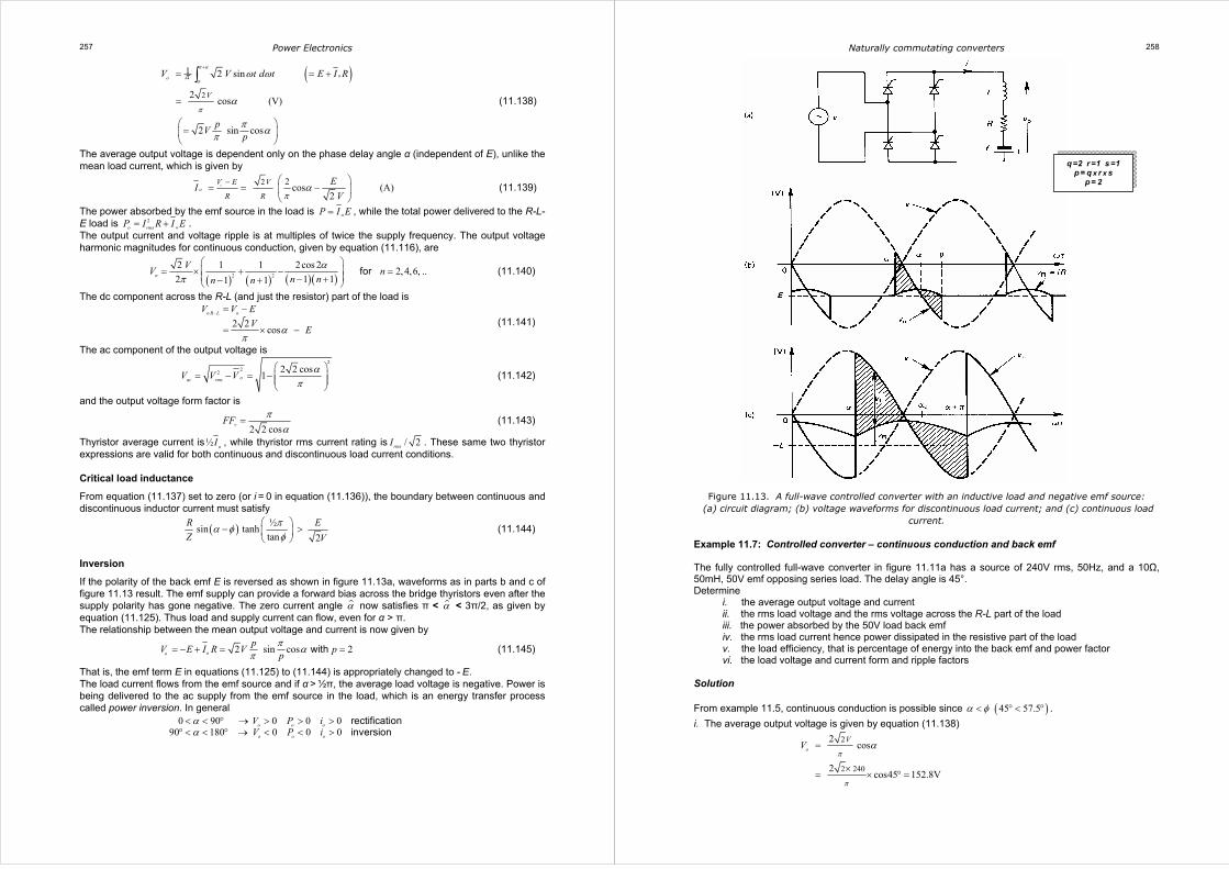
Power Electronics 257
( )2
1 2 sin
2 cos (V)
2 sin cos
π α
α
π
π ω ω
α
π απ
+
= = +
=
=
∫ oo
V
V V t d t E I R
pV
p
(11.138)
The average output voltage is dependent only on the phase delay angle α (independent of E), unlike the mean load current, which is given by
2 2 cos (A)
2o
oV E V
R R
EI
Vπα−
= = −
(11.139)
The power absorbed by the emf source in the load is oP I E= , while the total power delivered to the R-L-E load is 2= + oo rmsP I R I E . The output current and voltage ripple is at multiples of twice the supply frequency. The output voltage harmonic magnitudes for continuous conduction, given by equation (11.116), are
( ) ( ) ( )( )2 2
2 1 1 2cos 2 2, 4,6, ..2 1 11 1
απ
= × + − = − +− +
n
VV n
n nn nfor (11.140)
The dc component across the R-L (and just the resistor) part of the load is
.2 2 cos
o R L oV V E
VEα
π
− = −
= × − (11.141)
The ac component of the output voltage is
222 2 2 cos1 α
π
= − = −
oac rmsV V V (11.142)
and the output voltage form factor is
2 2 cos
πα
=vFF (11.143)
Thyristor average current is½o
I , while thyristor rms current rating is / 2rmsI . These same two thyristor expressions are valid for both continuous and discontinuous load current conditions. Critical load inductance From equation (11.137) set to zero (or i = 0 in equation (11.136)), the boundary between continuous and discontinuous inductor current must satisfy
( ) ½sin tanhtan 2πα φφ
− >
R E
Z V (11.144)
Inversion If the polarity of the back emf E is reversed as shown in figure 11.13a, waveforms as in parts b and c of figure 11.13 result. The emf supply can provide a forward bias across the bridge thyristors even after the supply polarity has gone negative. The zero current angle α now satisfies π < α < 3π/2, as given by equation (11.125). Thus load and supply current can flow, even for α > π. The relationship between the mean output voltage and current is now given by
2 sin cos 2π απ= − + = =with oo
pV E I R V p
p (11.145)
That is, the emf term E in equations (11.125) to (11.144) is appropriately changed to - E. The load current flows from the emf source and if α > ½π, the average load voltage is negative. Power is being delivered to the ac supply from the emf source in the load, which is an energy transfer process called power inversion. In general
0 90 0 0 0
90 180 0 0 0αα
< < ° → > > >° < < ° → < < >
rectificationinversion
o o o
o o o
V P iV P i
Naturally commutating converters 258
T1 T3
T2 T4
α
α
q =2 r =1 s =1 p = q x r x s
p = 2
Figure 11.13. A full-wave controlled converter with an inductive load and negative emf source: (a) circuit diagram; (b) voltage waveforms for discontinuous load current; and (c) continuous load
current. Example 11.7: Controlled converter – continuous conduction and back emf The fully controlled full-wave converter in figure 11.11a has a source of 240V rms, 50Hz, and a 10Ω, 50mH, 50V emf opposing series load. The delay angle is 45°. Determine
i. the average output voltage and current ii. the rms load voltage and the rms voltage across the R-L part of the load iii. the power absorbed by the 50V load back emf iv. the rms load current hence power dissipated in the resistive part of the load v. the load efficiency, that is percentage of energy into the back emf and power factor vi. the load voltage and current form and ripple factors
Solution From example 11.5, continuous conduction is possible since ( )45 57.5α φ< ° < ° .
i. The average output voltage is given by equation (11.138)
2
2 240
2 cos
2 cos45 152.8V
o
VV
π
π
α=
×= × ° =
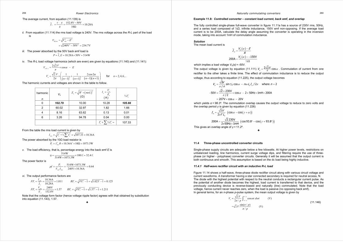
Power Electronics 259
The average current, from equation (11.139) is
152.8V 50V 10.28A
10o
oV E
RI
− −= = =
Ω
ii. From equation (11.114) the rms load voltage is 240V. The rms voltage across the R-L part of the load is
2 2
2 2240V 50V 234.7V
RLrms rmsV V E= −
= − =
iii. The power absorbed by the 50V back emf load is
10.28A 50V 514WoP I E= = × = iv. The R-L load voltage harmonics (which are even) are given by equations (11.140) and (11.141):
( ) ( ) ( )( )
.
2 2
2 2 cos
2 1 1 2cos 2 2, 4,6,..2 1 11 1
απ
απ
− = × −
= × + − = − +− +
for
o R L
n
VV E
VV n
n nn n
The harmonic currents and voltages are shown in the table to follow.
harmonic
n
Vn ( )
( )
22 ω= +nZ R n L
Ω
( )
= nn
n
VI
ZA
2½ nI
0 102.79 10.00 10.28 105.66
2 60.02 32.97 1.82 1.66
4 8.16 63.62 0.13 0.01
6 3.26 94.78 0.04 0.00
2 2½o nI I+ =∑ 107.33
From the table the rms load current is given by
2 2+½ 107.33 10.36A= = =∑rms o nI I I
The power absorbed by the 10Ω load resistor is 2 210.36A 10 1073.3W= = × Ω =L rmsP I R
v. The load efficiency, that is, percentage energy into the back emf E is
o oo o
514W 100 32.4514W 1073.3W
η = × =+
The power factor is
514W+1073.3W 0.64240V 10.36A
= = =×
L
rms rms
Ppf
V I
vi. The output performance factors are
2 2
2 2
10.36A 1.011 1 1.023 1 0.12510.28A
240V 1.57 1 1.57 1 1.211152.8V
= = = = − = − =
= = = = − = − =
rmsi i i
o
rmsv v v
o
IFF RF FF
IV
FF RF FFV
Note that the voltage form factor (hence voltage ripple factor) agrees with that obtained by substitution into equation (11.143), 1.57.
♣
Naturally commutating converters 260
Example 11.8: Controlled converter – constant load current, back emf, and overlap The fully controlled single-phase full-wave converter in figure 11.11a has a source of 230V rms, 50Hz, and a series load composed of ½Ω, infinite inductance, 150V emf non-opposing. If the average load current is to be 200A, calculate the delay angle assuming the converter is operating in the inversion mode, taking into account 1mH of commutation inductance. Solution The mean load current is
( )
( )½
150V200A
oo
o
V EI
RV
α
α
−=
− −=
Ω
which implies a load voltage Vo(α) = -50V.
The output voltage is given by equation (11.111) 22 cosoVV απ= . Commutation of current from one
rectifier to the other takes a finite time. The effect of commutation inductance is to reduce the output
voltage, thus according to equation (11.225), the output voltage becomes
2sin cos / 2 where 2
/
2 230V50V cos 2 50Hz 1mH 200A
/2207V cos 20V
o c onVV n L I nn
π α ω ππ
απ
α
= − =
×− = × − × × ×
= × −
which yields α = 98.3º. The commutation overlap causes the output voltage to reduce to zero volts and the overlap period γ is given by equation (11.226)
( )( )
( )( )
2cos cos
2
2 230V200A cos 93.8 cos 93.8
2 50Hz 1mH
oc
VIf L
α γ απ
γπ
= − +
= ° − + °×
This gives an overlap angle of γ = 11.2º. ♣
11.4 Three-phase uncontrolled converter circuits Single-phase supply circuits are adequate below a few kilowatts. At higher power levels, restrictions on unbalanced loading, line harmonics, current surge voltage dips, and filtering require the use of three-phase (or higher - polyphase) converter circuits. Generally it will be assumed that the output current is both continuous and smooth. This assumption is based on the dc load being highly inductive. 11.4.1 Half-wave rectifier circuit with an inductive R-L load Figure 11.14 shows a half-wave, three-phase diode rectifier circuit along with various circuit voltage and current waveforms. A transformer having a star connected secondary is required for neutral access, N. The diode with the highest potential with respect to the neutral conducts a rectangular current pulse. As the potential of another diode becomes the highest, load current is transferred to that device, and the previously conducting device is reverse-biased and naturally (line) commutated. Note that the load voltage, hence current never reaches zero, when the load is passive (no opposing back emf). In general terms, for an n-phase p-pulse system, the mean output voltage is given by
/
/
2
2
cos (V)2 /
sin( / )= (V)/
π
πω ω
ππ
π
−= ∫
p
op
VV t d t
p
pV
p
(11.146)

Power Electronics 261
ωt 2
3π
23
π
23
πN
a
c
b
π
π
π
q =3 r =1 s =1 p = q x r x s
p = 3
Figure 11.14. Three-phase half-wave rectifier: (a) circuit diagram and (b) circuit voltage and current waveforms.
For a three-phase, half-wave circuit (p = 3) the mean output voltage, (thence average current) is
5 / 6
2 / 63
1 2 sin
½ 32 1.17 (V)/ 3
π
π πω ω
π
= =
= = ×
∫ooV I R V t d t
V V (11.147)
The rms load voltage is
( )2 5 / 6
22 / 63
2 23 31 sin 1.19
2 3 4π
π π
πω ωπ
= = + = ×
∫rmsV V t d t V V (11.148)
The load form factor is
1.19 /1.17 1.01rmsFF
VV V VV= = = (11.149)
1 0.185= − =ac voltage across the load
RF = ripple factor = dc voltage across the load
rmsVV
(11.150)
Naturally commutating converters 262
R-L
q =3 r =1 s =1 p = q x r x s
p = 3
iR
iY
iB
1:N:N
( )
( )
( )
0
a c R
b a Y
c b B
R Y B
mmf N i i i
mmf N i i i
mmf N i i i
i i i mmf
= − +
= − +
= − +
+ + = =
Figure 11.15. Three-phase zig-zag interconnected star winding, with three windings per limb, 1:N:N: (a) transformer connection showing zero dc mmf in each limb (phase) and
(b) phasor diagram of transformer voltages. The diode conduction angle is 2π/n, namely ⅔π. The peak diode reverse voltage is given by the maximum voltage between any two phases, √3√2 V = √6 V. From equations (11.45), (11.46), and (11.47), for a constant output current, o o rmsI I= , the mean diode current is
1 13 (A)D o o
nI I I= = (11.151)
and the rms diode current is
31 1 1 (A)= ≈ =o oD o rms nnI I I I (11.152)
The diode current form factor is
/ 3= =DID DFF I I (11.153)
If neutral is available, a transformer is not necessary. The full load current is returned via the neutral supply. This neutral supply current is generally not acceptable other than at low power levels. The simple delta-star connection of the supply in figure 11.14a is not appropriate since the unidirectional current in each phase is transferred from the supply to the transformer. This may result in increased magnetising current and iron losses if dc magnetisation occurs. This problem is avoided in most cases by the special interconnected star winding, called zig-zag, shown in figure 11.15a. Each transformer limb has two equal voltage secondaries which are connected such that the magnetising forces balance. The resultant phasor diagram is shown in figure 11.15b. 15% more turns are needed than with a star connection.
As the number of phases increases, the windings become less utilised per cycle since the diode conduction angle decreases, from π for a single-phase circuit, to ⅔π for the three-phase case. 11.4.2 Full-wave rectifier circuit with an inductive R-L load Figure 11.16a shows a three-phase full-wave rectifier circuit where no neutral is necessary and it will be seen that two series diodes are always conducting. One diode (one of D1, D3, or D5, at the highest potential) can be considered as being in the feed circuit, while the other (one of D2, D4, or D6, at the lowest potential) is in the return circuit. As such, the line-to-line voltage is impressed across the load.
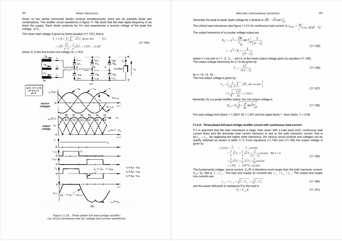
Power Electronics 263
Given no two series connected diodes conduct simultaneously, there are six possible diode pair combinations. The rectifier circuit waveforms in figure 11.16b show that the load ripple frequency is six times the supply. Each diode conducts for ⅔π and experiences a reverse voltage of the peak line voltage, √2 VL. The mean load voltage is given by twice equation (11.147), that is
2 / 3
/ 33
32 2
1 2 sin (V)
3 1.35 2.34/ 3
π
π πω ω
π π
= =
= = = =
∫o o L
L L
V I R V t d t
V V V V (11.154)
where VL is the line-to-line rms voltage (VL =√3V).
Figure 11.16. Three-phase full-wave bridge rectifier: (a) circuit connection and (b) voltage and current waveforms.
q =3 r =1 s =2 p = q x r x s
p = 6
ab ac bc ba ca ca 6,1 1,2 2,3 3,4 4,5 5,6
i a = iD1 - i D4
i b = iD3 - i D6
i c = iD5 - i D2
source voltages
output voltage
a b c
Naturally commutating converters 264
Generally the peak-to-peak ripple voltage for n-phases is 2 2 cosV nπ− .
The critical load inductance (see figure 11.21) for continuous load current, is ( )232 1critical
RL p pω= −×.
The output harmonics of a p-pulse voltage output are
2
2
2 2sin1
1
21
1
np
an
np
o
VV p np
Vn
ππ
= ×− −
= × ×− −
(11.155)
where n = mp and m = 1, 2, 3, … and Vo is the mean output voltage given by equation (11.146). The output voltage harmonics for p = 6 are given by
( )2
61
Lo n
VV
nπ=
− (11.156)
for n = 6, 12, 18, .. The rms output voltage is given by
.
2 / 32
/ 3
½1 2 sin2 / 6
3 31 1.3522
rms L
L L
V V t d t
V V
π
πω ω
π
π
=
= + =
∫ (11.157)
Generally, for a p-pulse rectifier output, the rms output voltage is
21 sin2rms L
pV V pπ
π= + (11.158)
The load voltage form factor = 1.352/1.35 = 1.001 and the ripple factor = √form factor -1 = 0.06.
11.4.2i Three-phase full-wave bridge rectifier circuit with continuous load current
If it is assumed that the load inductance is large, then (even with a load back emf), continuous load current flows and the dominate load current harmonic is due to the sixth harmonic current, that is let , ,6=o ac oI I . By neglecting the higher order harmonics, the various circuit currents and voltages can be readily obtained as shown in table 11.3. From equations (11.154) and (11.156) the output voltage is given by
( )
( )
, 6
22 2
2 2
cos 63 3 2 cos 6
13 3 2 cos 235
1.35 0.077 cos 2
ω ω
ωπ π
ωπ πω
= +
= + =−
= + ×
= +
o oo
L L
L L
L L
v t V V t
V V n t nn
V V t
V V t
for (11.159)
The fundamental voltage, hence current, Vo /R, is therefore much larger than the sixth harmonic current, Vo,6 / Z6, that is , 6>o oI I . The load and supply ac currents are , , , 6= =o ac s ac oI I I . The output and supply rms currents are
2 22 2
, , , , 6= = + = +o oo rms s rms o ac oI I I I II (11.160)
and the power delivered to resistance R in the load is 2
,=R o rmsP I R (11.161)
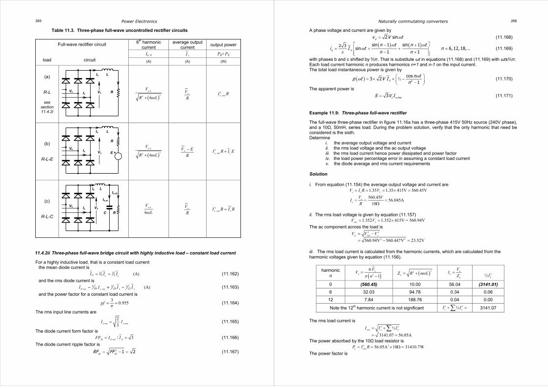
Power Electronics 265
Table 11.3. Three-phase full-wave uncontrolled rectifier circuits
6th harmonic current
average output current
output power
Io, 6 oI PR+PE
Full-wave rectifier circuit
load circuit (A) (A) (W)
(a)
R-L
see section 11.4.2i
( ), 6
22 6ω+
oV
R L oV
R
2, o rmsI R
(b)
R-L-E
( ), 6
22 6ω+
oV
R L −oV E
R
2, + oo rmsI R I E
(c)
R-L-C
, 6
6ωoV
L oV
R
22, = oo rmsI R I R
11.4.2ii Three-phase full-wave bridge circuit with highly inductive load – constant load current For a highly inductive load, that is a constant load current:
the mean diode current is
1 13 (A)D o o
nI I I= = (11.162)
and the rms diode current is
31 1 1 (A)= ≈ =o oD rms o rmsn nI I I I (11.163)
and the power factor for a constant load current is
3 0.955pf π= = (11.164)
The rms input line currents are
23
=L rms o rmsI I (11.165)
The diode current form factor is
/ 3= =DID D rmsFF I I (11.166)
The diode current ripple factor is
2 1 2ID ID
RF FF= − = (11.167)
Vs Is
Io
Vo
Io,dc
Io,ac
L
C R
Vs Is
Io
Vo E +
L
R
Vs Is
Io
Vo
L
R
Naturally commutating converters 266
A phase voltage and current are given by
2 sinav V tω= (11.168)
( ) ( )2 3 sin 1 sin 1
sin 6, 12,18, ..1 1oa
n t n ti I t n
n nπ
ω ωω
− += + + =
− + (11.169)
with phases b and c shifted by ⅔π. That is substitute ωt in equations (11.168) and (11.169) with ωt±⅔π. Each load current harmonic n produces harmonics n+1 and n-1 on the input current. The total load instantaneous power is given by
( ) ½2
cos3 2
1on t
p t V In
ωω = × × − −
(11.170)
The apparent power is
3 L s rmsS V I= (11.171)
Example 11.9: Three-phase full-wave rectifier The full-wave three-phase rectifier in figure 11.16a has a three-phase 415V 50Hz source (240V phase), and a 10Ω, 50mH, series load. During the problem solution, verify that the only harmonic that need be considered is the sixth. Determine
i. the average output voltage and current ii. the rms load voltage and the ac output voltage iii. the rms load current hence power dissipated and power factor iv. the load power percentage error in assuming a constant load current v. the diode average and rms current requirements
Solution i. From equation (11.154) the average output voltage and current are
1.35 1.35 415V 560.45V560.45 56.045A
10
= = = × =
= = =Ω
o o L
oo
V I R V
V VI
R
ii. The rms load voltage is given by equation (11.157) 1.352 1.352 415V = 560.94Vrms LV V= = ×
The ac component across the load is
2 2
2 2560.94V 560.447V 23.52V= −= − =
ac rms oV V V
iii. The rms load current is calculated from the harmonic currents, which are calculated from the harmonic voltages given by equation (11.156).
harmonic n ( )2
61
Ln
VV
nπ=
− ( )22
nZ R n Lω= + n
n
n
VI
Z=
2½ nI
0 (560.45) 10.00 56.04 (3141.01)
6 32.03 94.78 0.34 0.06
12 7.84 188.76 0.04 0.00
Note the 12th harmonic current is not significant 2 2½o nI I+ =∑ 3141.07
The rms load current is
.
2 2½3141.07 56.05A
rms o nI I I= +
= =∑
The power absorbed by the 10Ω load resistor is 2 256.05A 10 31410.7WL rmsP I R= = × Ω =
The power factor is
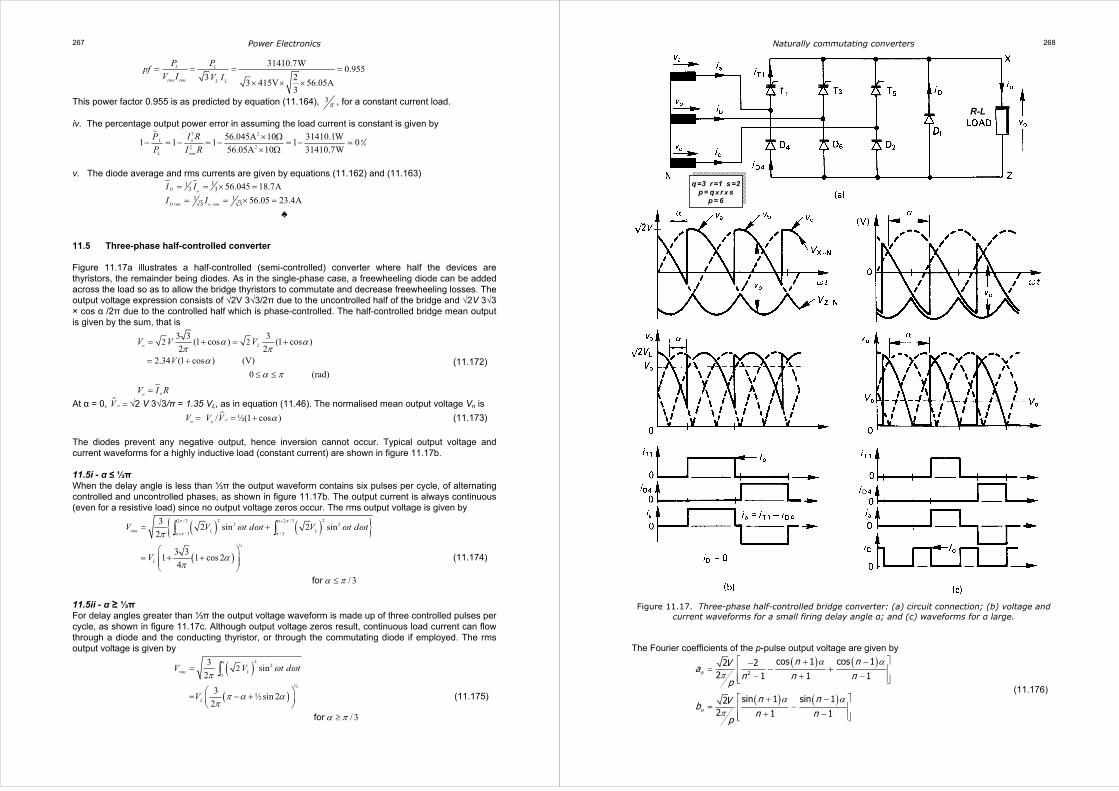
Power Electronics 267
31410.7W 0.955
3 23 415V 56.05A3
= = = =× × ×
L L
rms rms L L
P Ppf
V I V I
This power factor 0.955 is as predicted by equation (11.164), 3π , for a constant current load. iv. The percentage output power error in assuming the load current is constant is given by
2 2
oo2 2
56.045A 10 31410.1W1 1 1 1 056.05A 10 31410.7W
× Ω− = − = − = −
× ΩoL
L rms
I RP
P I R
v. The diode average and rms currents are given by equations (11.162) and (11.163)
11
3 31 1
3 3
56.045 18.7A56.05 23.4A
= = × == = × =
D o
D rms o rms
I I
I I
♣
11.5 Three-phase half-controlled converter Figure 11.17a illustrates a half-controlled (semi-controlled) converter where half the devices are thyristors, the remainder being diodes. As in the single-phase case, a freewheeling diode can be added across the load so as to allow the bridge thyristors to commutate and decrease freewheeling losses. The output voltage expression consists of √2V 3√3/2π due to the uncontrolled half of the bridge and √2V 3√3 × cos α /2π due to the controlled half which is phase-controlled. The half-controlled bridge mean output is given by the sum, that is
2 23 3 3(1 cos ) (1 cos )2 2
2.34 (1 cos ) (V)0 (rad)
α απ π
αα π
= + = +
= +≤ ≤
=
o L
oo
V V V
V
V I R
(11.172)
At α = 0, oV = √2 V 3√3/π = 1.35 VL, as in equation (11.46). The normalised mean output voltage Vn is
/ ½(1 cos )on oV V V α= = + (11.173)
The diodes prevent any negative output, hence inversion cannot occur. Typical output voltage and current waveforms for a highly inductive load (constant current) are shown in figure 11.17b. 11.5i - α ≤ ⅓π When the delay angle is less than ⅓π the output waveform contains six pulses per cycle, of alternating controlled and uncontrolled phases, as shown in figure 11.17b. The output current is always continuous (even for a resistive load) since no output voltage zeros occur. The rms output voltage is given by
( ) ( ) ( )
2 22 / 3 2 / 32 2
/ 3 / 3
½
3 2 sin 2 sin2
3 31 1 cos 24
/ 3
π α π
α π πω ω ω ω
π
απ
α π
+
+= +
= + +
≤
∫ ∫
for
rms L L
L
V V t d t V t d t
V (11.174)
11.5ii - α ≥ ⅓π For delay angles greater than ⅓π the output voltage waveform is made up of three controlled pulses per cycle, as shown in figure 11.17c. Although output voltage zeros result, continuous load current can flow through a diode and the conducting thyristor, or through the commutating diode if employed. The rms output voltage is given by
( )
( )
22
½
23 sin
2
3 ½ sin 22
/ 3
π
αω ω
π
π α απ
α π
=
= − +
≥
∫rms L
L
V V t d t
V
for
(11.175)
Naturally commutating converters 268
Figure 11.17. Three-phase half-controlled bridge converter: (a) circuit connection; (b) voltage and
current waveforms for a small firing delay angle α; and (c) waveforms for α large. The Fourier coefficients of the p-pulse output voltage are given by
( ) ( )
( ) ( )
2
cos 1 cos 12 22 1 1 1
sin 1 sin 122 1 1
n
n
n nVa
n n np
n nVbn n
p
α απ
α απ
+ −−= − +
− + −
+ −= −
+ −
(11.176)
R-L
q =3 r =1 s =2 p = q x r x s
p = 6

Power Electronics 269
q =3 r =1 s =1 p = q x r x s
p = 3
where n = mp and m = 1, 2, 3, .. For the three-phase, full-wave, half-controlled case, p = 6, thus the output voltage harmonics occur at n = 6, 12, … 11.6 Three-phase, fully controlled thyristor converter circuits 11.6.1 Half-wave, fully-controlled circuit with an inductive load When the diodes in the circuit of figure 11.14 are replaced by thyristors, as in figure 11.18a, a three-phase fully controlled half-wave converter results. The output voltage is controlled by the delay angle α. This angle is specified from the thyristor commutation angle, which is the earliest point the associated thyristor becomes forward-biased, as shown in parts b, c, and d of figure 11.18. (The reference is not the phase zero voltage cross-over point). The thyristor with the highest instantaneous anode potential will conduct when fired and in turning on will reverse bias and turn off any previously conducting thyristor. The output voltage ripple is three times the supply frequency and the supply currents contain dc compo-nents. Each phase progressively conducts for periods of π, displaced by α, as shown in figure 11.18b.
Figure 11.18. Three-phase half-wave controlled converter: (a) circuit connection; (b) voltage and current waveforms for a small firing delay angle α; (c) and (d)
load voltage waveforms for progressively larger delay angles.
Naturally commutating converters 270
q =3 r =1 s =1 p = q x r x s
p = 3
Df
The mean output voltage for an n-phase half-wave controlled converter is given by (see example 11.8)
/
/
2
2
cos2 /
sin( / ) cos (V)/
n
on
VV t d t
nn
Vn
α π
α πω ω
ππ α
π
+
−=
=
∫ (11.177)
which for the three-phase circuit considered with continuous or discontinuous (R) load current gives
3
23 cos 1.17 cos 0 / 62ooV I R V Vα α α ππ
= = = ≤ ≤ (11.178)
For discontinuous conduction, and a resitive load, the mean output voltage is
( )( )23 1 cos / 6 / 6 5 / 6
2α π π α π
π= = + + ≤ ≤ooV I R V (11.179)
The mean output voltage is zero for α = ½π. For 0 < α < π, the instantaneous output voltage is always greater than zero. Negative average output voltage occurs when α > ½π as shown in figure 11.18d. Since the load current direction is unchanged, for α > ½π, power reversal occurs, with energy feeding from the load into the ac supply. Power inversion assumes a load with an emf to assist the current flow, as in figure 11.13. If α > π no reverse bias exists for natural commutation and continuous load current will freewheel. The maximum mean output voltage oV = √2V 3√3 /2π occurs at α = 0. The normalised mean output voltage Vn is
ˆ/ cosn o oV V V α= = (11.180)
With an R-L load, at Vo = 0, the load current falls to zero. Thus for α > ½π, continuous load current does not flow for an R-L load. The rms output voltage is given by
( )2 /3
2
/3
½1 36 8
2
3 2
3 sin ( )2
sin 2
rmsV V t d t
V
α π
α π
π
ω ωπ
α
+
−=
= +
∫ (11.181)
From equations (11.178) and (11.181), the ac in the output voltage is
2 2½
1 3 36 8 2
3 2 2sin2 cosac rms oV V V Vπ π
α α = − = + −
(11.182)
The output voltage distortion ripple factor is
( ) ( )2 32
27 18(min at =0 = 0.173; max at =½π = 0.66)2sin2 cos vRF ππ α αα α= + − (11.183)
11.6.2 Half-wave converter with freewheel diode
Figure 11.19 shows a three-phase, half-wave controlled rectifier converter circuit with a load freewheel diode, Df. This diode prevents the load voltage from going negative, thus inversion is not possible.
Figure 11.19. A half-wave fully controlled three-phase converter with a load freewheel diode.
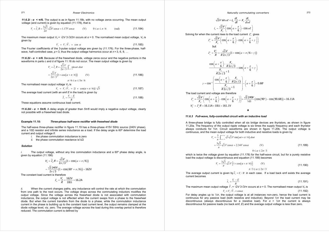
Power Electronics 271
11.6.2i - α < π/6. The output is as in figure 11.18b, with no voltage zeros occurring. The mean output voltage (and current) is given by equation (11.178), that is
3 3 2 cos 1.17 cos (V) 0 / 6 (rad)2
α α α ππ
= = = ≤ ≤ooV I R V V (11.184)
The maximum mean output Vo = √2V 3√3/2π occurs at α = 0. The normalised mean output voltage, Vn is given by
/ cos on oV V V α= = (11.185)
The Fourier coefficients of the 3-pulse output voltage are given by (11.176). For the three-phase, half-wave, half-controlled case, p = 3, thus the output voltage harmonics occur at n = 3, 6, 9, … 11.6.2ii - α > π/6. Because of the freewheel diode, voltage zeros occur and the negative portions in the waveforms in parts c and d of figure 11.18 do not occur. The mean output voltage is given by
( )( )
/ 6
2
2
sin2 / 3
1 cos / 6 (V)2 / 3
/ 6 5 / 6
π
α πω ω
π
α ππ
π α π
−= =
= + +
≤ ≤
∫oo
VV I R t d t
V (11.186)
The normalised mean output voltage Vn is
/ [1 cos( / 6)]/ 3on oV V V α π= = + + (11.187)
The average load current (with an emf E in the load) is given by
oo
V EI
R
−= (11.188)
These equations assume continuous load current. 11.6.2iii - α > 5π/6. A delay angle of greater than 5π/6 would imply a negative output voltage, clearly not possible with a freewheel load diode. Example 11.10: Three-phase half-wave rectifier with freewheel diode The half-wave three-phase rectifier in figure 11.19 has a three-phase 415V 50Hz source (240V phase), and a 10Ω resistor and infinite series inductance as a load. If the delay angle is 60º determine the load current and output voltage if:
i. the phase commutation inductance is zero ii. the phase commutation reactance is¼Ω
Solution i. The output voltage, without any line commutation inductance and a 60º phase delay angle, is given by equation (11.186)
( )( )
( )( )
2
2 240
1 cos / 62 / 3
V1 cos 60 / 6 162V
2 / 3
oo
VV I R α π
π
ππ
= = + +
= + ° + =
The constant load current is therefore
162V
16.2A10
oo
VI
R= = =
Ω
ii. When the current changes paths, any inductance will control the rate at which the commutation from one path to the next occurs. The voltage drops across the commutating inductors modifies the output voltage. Since the voltage across the freewheel diode is not associated with commutation inductance, the output voltage is not effected when the current swaps from a phase to the freewheel diode. But when the current transfers from the diode to a phase, while the commutation inductance current in the phase is building up to the constant load current level, the output remains clamped at the diode voltage level, viz. zero. The average voltage across the load during this overlap period is therefore reduced. The commutation current is defined by
Naturally commutating converters 272
2 sin c cc c
di diV t L X
dt d tω
ω= =
2
cos cos6c
c
Vi t
Xπα ω
= + −
Solving for when the current rises to the load current oI γ gives
( )( )2
2cos cos
6 6
but
1 cos / 62 / 3
o
o
c
o
VI
X
V VIR R
γ
γγ
π πα α γ
α π γπ
= + − + +
= = + + +
cos6 2 / 3
cos61
2 / 3
c
c
XR
XR
παππ α γ
π
+ − = + + +
1
cos6 2 / 3
cos 0.6861
2 / 3
c
c
XR
XR
παππγ α
π
−
+ − = − + = ° +
The load current and voltage are therefore
( ) ( )( )
¼2 2 240
cos cos cos 90 cos 90.68 16.11A6 6
16.11A 10 161.1V
o
o
c
o
V VIX
V I R
γ
γ γ
π πα α γ = + − + + = ° − = Ω
= = × Ω =
♣ 11.6.3 Full-wave, fully-controlled circuit with an inductive load
A three-phase bridge is fully controlled when all six bridge devices are thyristors, as shown in figure 11.20a. The frequency of the output ripple voltage is six times the supply frequency and each thyristor always conducts for ⅔π. Circuit waveforms are shown in figure 11.20b. The output voltage is continuous, and the mean output voltage for both inductive and resistive loads is given by
( ) ½
/ 63 2
32
3 sin / 6
3 cos 2.34 cos (V)
0 2 / 3
α π
α πω π ω
π
α απ
α π
+
+= +
= =
≤ ≤
∫oV V t d t
V V (11.189)
which is twice the voltage given by equation (11.178) for the half-wave circuit, but for a purely resistive load the output voltage is discontinuous and equation (11.189) becomes
( )32
3 1 cos / 6 (V)
/ 3 2 / 3
α ππ
π α π
= + +
≤ ≤
oV V (11.190)
The average output current is given by /ooI V R= in each case. If a load back emf exists the average current becomes
o
o
V EI
R
−= (11.191)
The maximum mean output voltage oV = √2V 3√3/π occurs at α = 0. The normalised mean output Vn is
/ coson oV V V α= = (11.192)
For delay angles up to ⅓π, the output voltage is at all instances non-zero, hence the load current is continuous for any passive load (both resistive and inductive). Beyond ⅓π the load current may be discontinuous (always discontinuous for a resistive load). For α > ½π the current is always discontinuous for passive loads (no back emf, E) and the average output voltage is less than zero.
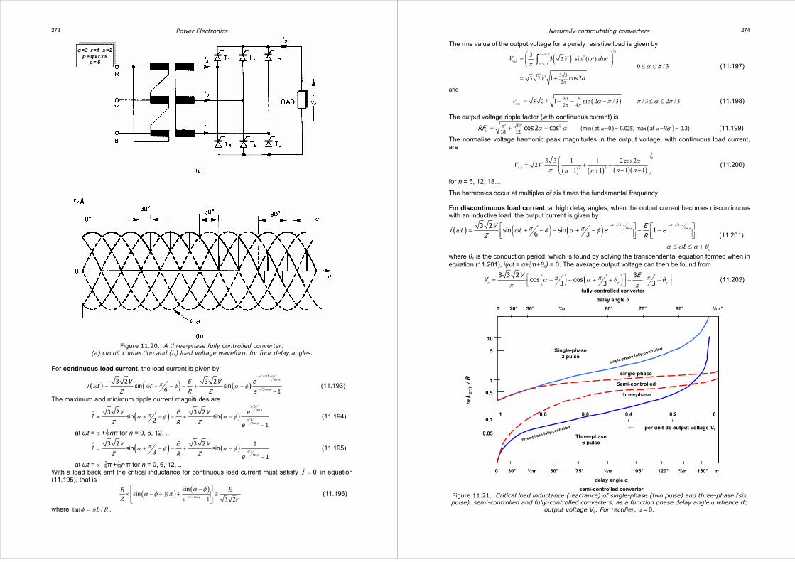
Power Electronics 273
Figure 11.20. A three-phase fully controlled converter: (a) circuit connection and (b) load voltage waveform for four delay angles.
For continuous load current, the load current is given by
( ) ( ) ( )6
tan
3 tan
3 2 3 2sin sin
6 1
t
V E V ei t t
Z R Z e
ω π αφ
π φπω ω φ α φ
− + +
−= + − − + −
− (11.193)
The maximum and minimum ripple current magnitudes are
( ) ( )6
tan
3tan
3 2 3 2sin sin
21
V E V eI
Z R Z e
πφ
πφ
πα φ α φ−
= + − − + −−
(11.194)
at ωt = α +nπ for n = 0, 6, 12, ..
( ) ( ) 3tan
3 2 3 2 1sin sin
31
V E VI
Z R Z eπ
φ
πα φ α φ−
= + − − + −−
∨
(11.195)
at ωt = α - π +n π for n = 0, 6, 12, .. With a load back emf the critical inductance for continuous load current must satisfy 0I
∨
= in equation (11.195), that is
( ) ( )/ 3 tan
13
sinsin
1 3 2R E
Z e Vπ φ
α φα φ π
−
− × − + + ≥ −
(11.196)
where tan /L Rφ ω= .
q =3 r =1 s =2 p = q x r x s
p = 6
Naturally commutating converters 274
The rms value of the output voltage for a purely resistive load is given by
( )2 / 2
2
/ 6
½
3 32
2
3 2
3 3 sin ( )
1 cos 2
rmsV V t d t
V
α π
α π
π
ω ωπ
α
+
−
=
= +
∫ 0 / 3α π≤ ≤ (11.197)
and
( )3 32 4
3 2 1 sin 2 / 3rmsV V απ π
α π= − − − / 3 2 / 3π α π≤ ≤ (11.198) The output voltage ripple factor (with continuous current) is
( ) ( )2 3 2
18 12(min at =0 = 0.025; max at =½π = 0.3)cos 2 cos vRF ππ α αα α= + − (11.199)
The normalise voltage harmonic peak magnitudes in the output voltage, with continuous load current, are
( ) ( ) ( )( )
.
.
12
2 2
3 3 1 1 2cos 221 11 1
απ
= + − − +− +
L nV Vn nn n
(11.200)
for n = 6, 12, 18… The harmonics occur at multiples of six times the fundamental frequency. For discontinuous load current, at high delay angles, when the output current becomes discontinuous with an inductive load, the output current is given by
( ) ( ) ( ) 6 6tan tan3 2
sin sin 16 3
t t
c
V Ei t t e e
Z R
t
ω π α ω π αφ φπ πω ω φ α φ
α ω α θ
− − + − − +
= + − − + − − −
≤ ≤ +
(11.201)
where θc is the conduction period, which is found by solving the transcendental equation formed when in equation (11.201), i(ωt = α+π+θc) = 0. The average output voltage can then be found from
( ) ( )3 3 2 3cos cos3 3 3o c c
V EV π π πα α θ θ
π π= + − + + − −
(11.202)
Figure 11.21. Critical load inductance (reactance) of single-phase (two pulse) and three-phase (six pulse), semi-controlled and fully-controlled converters, as a function phase delay angle α whence dc
output voltage Vo. For rectifier, α = 0.
Three-phase 6 pulse
0 30° ¼π 60° 75° ½π 105° 120° ¾π 150° π
delay angle α
semi-controlled converter
fully-controlled converter
delay angle α
0 20° 30° ¼π 60° 70° 80° ½π°
1 0.8 0.6 0.4 0.2 0
← per unit dc output voltage Vo
10
5
1
0.5
0.1
0.05
Single-phase 2 pulse
single-phase
Semi-controlled
three-phase
three-phase fully-controlled
single-phase fully-controlled
ωL
crit
/R
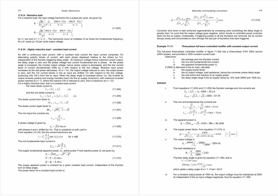
Power Electronics 275
11.6.3i - Resistive load For a resistive load, the load voltage harmonics for p pulses per cycle, are given by
( ) ( )
( ) ( )
2
cos 1 cos 12 22 1 1 1
sin 1 sin 122 1 1
n
n
n nVa
n n np
n nVbn n
p
α απ
α απ
+ −−= − −
+ + −
+ −= −
+ −
(11.203)
for n = pm and m = 1, 2, 3, .. The harmonics occur at multiples of six times the fundamental frequency, for a 6 - pulse (p = 6) per cycle output voltage. 11.6.3ii - Highly inductive load – constant load current As with a continuous load current, with a constant load current the input current comprises ⅔π alternating polarity blocks of current, with each phase displaced relative to the others by ⅔π, independent of the thyristor triggering delay angle. At maximum voltage hence maximum power output, the delay angle is zero and the phase voltage and current fundamental are in phase. As the phase angle is increased, the inverter output voltage, hence power output is decreased, and the line current block of current (fundamental) shifts by α with respect to the line voltage. Reactive input power increases as the real power decreases. At α = ½π, the output voltage reduces to zero, the output power is zero, and the ⅔π current blocks in the ac input are shifted ½π with respect to the line voltage, producing only VAr’s from the ac input. When the delay angle is increased above ½π, the inverter dc output reverses polarity and energy transfers back into the ac supply (inversion), with maximum inverted power reached at α = π, where the reactive VAr is reduced to zero, from a maximum at α = ½π. For a highly inductive load, that is a constant load current:
the mean diode current is
1 13 (A)= =Th o o
nI I I (11.204)
and the rms diode current is
31 1 1 (A)= ≈ =o oTh rms o rmsn nI I I I (11.205)
The diode current form factor is
/ 3= =ThITh Th rmsFF I I (11.206)
The diode current ripple factor is
2 1 2ITh ITh
RF FF= − = (11.207)
The rms input line currents are
23
=L rms o rmsI I (11.208)
A phase voltage is given by
2 sinav V tω= (11.209)
with phases b and c shifted by ⅔π. That is substitute ωt with ωt±⅔π. From equation (14.34), the line current harmonics are
( )½ 13
4 1cos for oddoi I n n
nπ
π=i (11.210)
The rms fundamental input current is
1
23 ormsI I
π= (11.211)
The supply fundamental apparent power, S1, active power P and reactive power Q, are given by
2 21 1
1 1
1 1
3
cos
sin
rmsS VI P Q
P P S
Q Q S
α
α
= = +
= =
= =
(11.212)
The supply apparent power is constant for a given constant load current, independent of the thyristor turn-on delay angle. The power factor for a constant load current is
Naturally commutating converters 276
1
23 3 cos3 cos 3 cos2 23 33 3
αα π απ
= = =× ×
ormsrms rms
o orms rms
V IV Ipf
V I V I
(11.213)
Converter shut down is best achieved regeneratively by increasing (and controlling) the delay angle to greater than ½π such that the output voltage goes negative, which results in controlled power inversion back into the ac supply. Undesirably, if triggering pulses to all the thyristors are removed, the dc current decays slowly and uncontrolled to zero through the last pair of thyristors that were triggered. Example 11.11: Three-phase full-wave controlled rectifier with constant output current The full-wave three-phase controlled rectifier in figure 11.20a has a three-phase 415V 50Hz source (240V phase), and provides a 100A constant current load.
Determine: i. the average and rms thyristor current ii. the rms and fundamental line current iii. the apparent fundamental power S1
If 25kW is delivered to the dc load, calculate: iv. the supply power factor iv. the dc output voltage, load resistance, hence the converter phase delay angle v. the real active and reactive Q1 ac supply power vi. the delay angle range if the ac supply varies by ±5% (with 25kW and 100A dc).
Solution
i. From equations (11.204) and (11.205) the thyristor average and rms currents are
1 1 13 3 3
1 13 3
100A 33 A
100A 57.7A
oTh
oTh rms
I I
I I
= = × =
= = × =
ii. The rms and fundamental line currents are
1
2 2 100A = 81.6A3 3
2 23 3 100A = 78.0Aπ π
= = ×
= = ×
L rms o rms
orms
I I
I I
iii. The apparent power is
1 13 3 415V 78A = 56.1kVArmsS VI= = × ×
iv. The supply power factor, from equation (11.213), is
25kW 30.426 cos
3 3 415V 81.6Aα
π = = = = × ×
L
rms rms
Ppf
V I
v. The output voltage is
power 25kW 250V dc100Aoo
VI
= = =
The load resistance is
250V
2.5100A
oL
o
VR
I= = = Ω
Thyristor delay angle is given by equation (11.189), that is
2.34 cos
415V250Vdc 2.34 cos3
α
α
=
= × ×
oV V
which yields a delay angle of α = 1.11rad = 63.5° vi. For a constant output power at 100A dc, the output voltage must be maintained at 250V
dc independent of the ac input voltage magnitude, thus for equation (11.189)
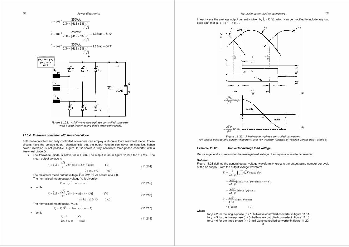
Power Electronics 277
q =3 r =1 s =2 p = q x r x s
p = 6
( )
( )
( )
1
1
1
250Vdccos
2.34 415 5%3
250Vdccos 1.08rad 61.9
2.34 415 5%3
250Vdccos 1.13rad 64.9
2.34 415 5%3
α
α
α
−
∨−
−
=× ±
= = = °× −
= = = °× +
♣
Figure 11.22. A full-wave three-phase controlled converter with a load freewheeling diode (half-controlled).
11.6.4 Full-wave converter with freewheel diode
Both half-controlled and fully controlled converters can employ a discrete load freewheel diode. These circuits have the voltage output characteristic that the output voltage can never go negative, hence power inversion is not possible. Figure 11.22 shows a fully controlled three-phase converter with a freewheel diode D.
• The freewheel diode is active for α > ⅓π. The output is as in figure 11.20b for α < ⅓π. The mean output voltage is
3
23 cos 2.34 cos (V)
0 / 3 (rad)
ooV I R V Vα απ
α π
= = =
≤ ≤ (11.214)
The maximum mean output voltage oV = √2V 3√3/π occurs at α = 0. The normalised mean output voltage Vn is given by
/ cos on oV V V α= = (11.215)
• while
( )( )32
3 1 cos / 3 (V)
/ 3 2 / 3 (rad)
ooV I R V α ππ
π α π
= = + +
≤ ≤ (11.216)
The normalised mean output, Vn, is
( ) / 1 cos / 3on oV V V α π= = + + (11.217)
• while
0 (V)
2 / 3 (rad)oV
π α=
≤ (11.218)
Naturally commutating converters 278
½ π π
2 s inV nn
ππ
2 s inV nn
ππ−
(a) (b)
π− p 0
π+ p
rectify
invert
2pπ
2sin
Vp
pππ+
2sin
V pp
ππ−
In each case the average output current is given by /ooI V R= , which can be modified to include any load back emf, that is, ( ) /ooI V E R= − .
Figure 11.23. A half-wave n-phase controlled converter:
(a) output voltage and current waveform and (b) transfer function of voltage versus delay angle α. Example 11.12: Converter average load voltage
Derive a general expression for the average load voltage of an p-pulse controlled converter.
Solution Figure 11.23 defines the general output voltage waveform where p is the output pulse number per cycle of the ac supply. From the output voltage waveform
( )
/
/2
2
2
1 cos2 /
sin( / ) sin( / )2 /
2sin( / ) cos2 /
π α
π αω ω
π
α π α ππ
π απ
+
− +=
= + − −
=
∫n
on
V V t d tp
Vp p
p
Vp
p
2 sin( / ) cos/
cos (V)
π απ
α
=
=
o
o
VV p
p
V
where for p = 2 for the single-phase (n = 1) full-wave controlled converter in figure 11.11. for p = 3 for the three-phase (n = 3) half-wave controlled converter in figure 11.18. for p = 6 for the three-phase (n = 3) full-wave controlled converter in figure 11.20.
♣
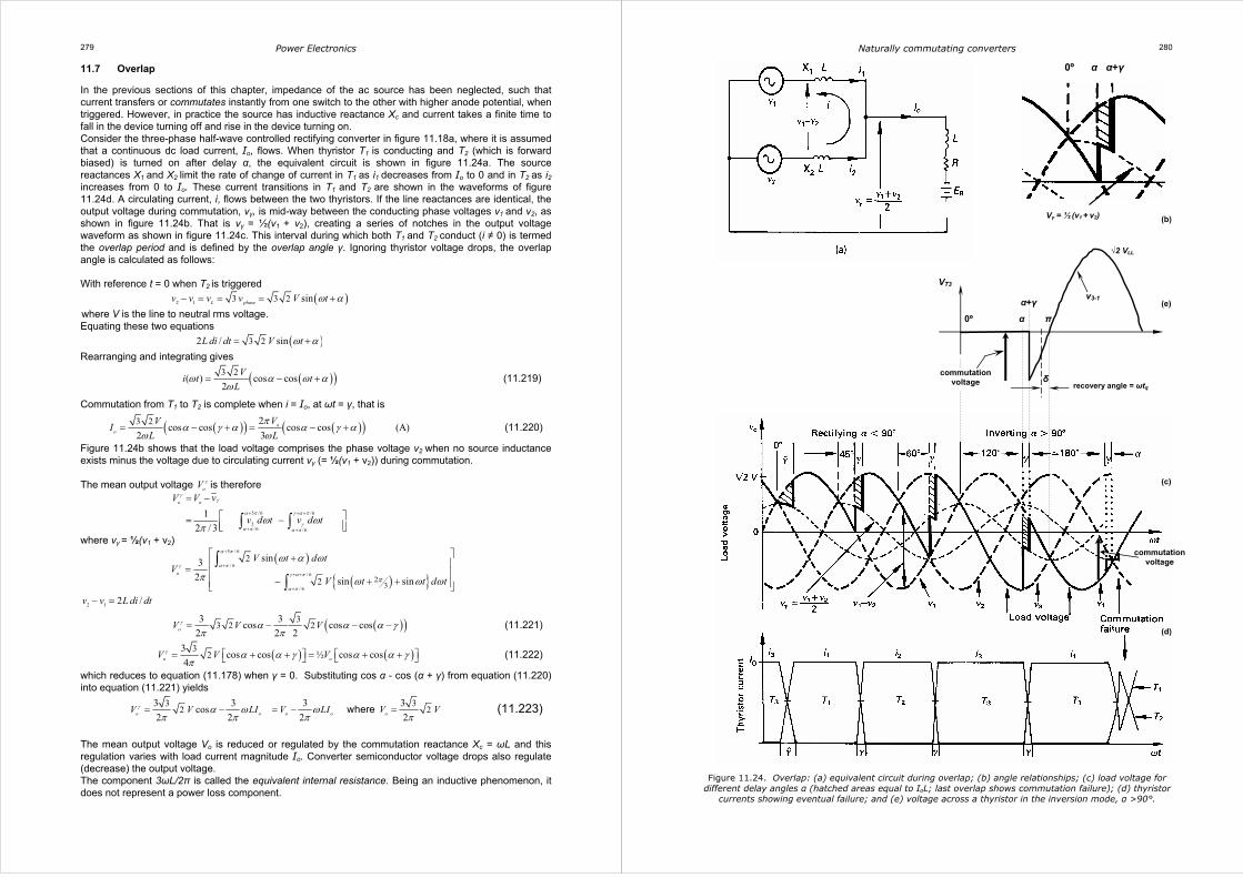
Power Electronics 279
11.7 Overlap
In the previous sections of this chapter, impedance of the ac source has been neglected, such that current transfers or commutates instantly from one switch to the other with higher anode potential, when triggered. However, in practice the source has inductive reactance Xc and current takes a finite time to fall in the device turning off and rise in the device turning on. Consider the three-phase half-wave controlled rectifying converter in figure 11.18a, where it is assumed that a continuous dc load current, Io, flows. When thyristor T1 is conducting and T2 (which is forward biased) is turned on after delay α, the equivalent circuit is shown in figure 11.24a. The source reactances X1 and X2 limit the rate of change of current in T1 as i1 decreases from Io to 0 and in T2 as i2
increases from 0 to Io. These current transitions in T1 and T2 are shown in the waveforms of figure 11.24d. A circulating current, i, flows between the two thyristors. If the line reactances are identical, the output voltage during commutation, vγ, is mid-way between the conducting phase voltages v1 and v2, as shown in figure 11.24b. That is vγ = ½(v1 + v2), creating a series of notches in the output voltage waveform as shown in figure 11.24c. This interval during which both T1 and T2 conduct (i ≠ 0) is termed the overlap period and is defined by the overlap angle γ. Ignoring thyristor voltage drops, the overlap angle is calculated as follows: With reference t = 0 when T2 is triggered
( )2 1 3 3 2 sinL phasev v v v V tω α− = = = +
where V is the line to neutral rms voltage. Equating these two equations
( )3 22 / sinL di dt V tω α= +
Rearranging and integrating gives
( )( )3 2( ) cos cos2
ω α ω αω
= − +V
i t tL
(11.219)
Commutation from T1 to T2 is complete when i = Io, at ωt = γ, that is
( )( ) ( )( )3 2 2cos cos cos cos (A)
2 3π
α γ α α γ αω ω
= − + = − +oo
VVI
L L (11.220)
Figure 11.24b shows that the load voltage comprises the phase voltage v2 when no source inductance exists minus the voltage due to circulating current vγ (= ½(v1 + v2)) during commutation. The mean output voltage oV γ is therefore
5 /6 /6
2 /6 /6
12 / 3
o ovV V
v d t v d t
γγ
α π γ α π
γα π α π
ω ωπ
+ + +
+ +
= −
= − ∫ ∫
where vγ = ½(v1 + v2)
( )
( )
5 / 6
/ 6
/ 6
/ 6
23
2
2
sin32 sin sin
α π
α πγ
γ α π
α π
π
ω α ω
π ω ω ω
+
+
+ +
+
+ = − + +
∫∫
o
V t d tV
V t t d t
2 1 2 /v v L di dt− =
( )( )33 2 2
3 3cos cos cos2 2 2oV V Vγ α α α γπ π
= − − − (11.221)
( ) ( )32
3 cos cos ½ cos cos4
γ α α γ α α γπ
= + + = + + o oV V V (11.222)
which reduces to equation (11.178) when γ = 0. Substituting cos α - cos (α + γ) from equation (11.220) into equation (11.221) yields
3 32 2
3 3 3 3cos2 2 2 2
γ α ω ωπ π π π
= − = − = where o o o o oV V LI V LI V V (11.223)
The mean output voltage Vo is reduced or regulated by the commutation reactance Xc = ωL and this regulation varies with load current magnitude Io. Converter semiconductor voltage drops also regulate (decrease) the output voltage. The component 3ωL/2π is called the equivalent internal resistance. Being an inductive phenomenon, it does not represent a power loss component.
Naturally commutating converters 280
Vγ = ½ (v1 + v2)
0º α α+γ
α+γ
0º α π
δ
v3-1
√2 VLL
recovery angle = ωtq
VT3
(b) (e) (c) (d)
commutation voltage
commutation voltage
Figure 11.24. Overlap: (a) equivalent circuit during overlap; (b) angle relationships; (c) load voltage for different delay angles α (hatched areas equal to IoL; last overlap shows commutation failure); (d) thyristor
currents showing eventual failure; and (e) voltage across a thyristor in the inversion mode, α >90°.

Power Electronics 281
As shown in figure 11.25, the overlap occurs immediately after the delay α. The commutation voltage, v2 - v1, is √3 √2 V sin α. The commutation time is inversely proportional to the commutation voltage v2 - v1. For rectification, as α increases from zero to ½π, the commutation voltage increases from a minimum of zero volts to a maximum of √3 √2 V at ½π, whence the overlap angle γ decreases from a maximum of γ∧
at α = 0 to a minimum of γ∨
at ½π. [For inversion, the overlap angle γ decreases from a minimum of γ
∨ at ½π to a maximum of γ
∧ at π, as
the commutation voltage reduces from a maximum, back to zero volts.] From equation (11.220), with α = π
2 3 sin(2 / )oarc LI Vγ ω∨
=
The general expressions for the mean load voltage oV γ of an n-pulse, fully-controlled converter, with underlap, are given by
( )2 sin cos cos2 /
γ π α α γπ
= + + o nV
Vn
(11.224)
and
2 sin cos / 2/
γ π α ππ
= ∓o c onV
V nX In
(11.225)
where V is the line voltage for a full-wave converter and the phase voltage for a half-wave converter and the plus sign in equation (11.225) accounts for inversion operation. Effectively, as shown in figure 11.26, during rectification, overlap reduces the mean output voltage by nfLIo or as if α were increased. The supply voltage is effectively distorted and the harmonic content of the output is increased. Equating equations (11.224) and (11.225) gives the mean output current
( )( )2 sin cos cos (A)o
c
nV
IX
π α γ α= − + (11.226)
which reduces to equation (11.220) when n = 3. Harmonic input current magnitudes are decreased by a factor ( )sin ½ /½n nγ γ . In the three-phase case, for a constant dc link current Io, without commutation effects, the rms phase current and the magnitude of the nth current harmonic are
2 2 3
3o
rms h n o
II I I
nπ= = (11.227)
When accounting for commutation reactance effects the fundamental current is
( ) ( )
( )
½2 2
1
cos 2 - cos 2 2 sin2 sin22 34 cos cosh oI I
α α γ γ α α γ
π α α γ
+ + + − + = − +
(11.228)
The single-phase, full-wave, converter voltage drop is 2ωLIo /π and the overlap output voltage is zero. The general effects of line inductance, which causes current overlap are:
• the average output voltage is reduced • the input voltage is distorted • the inversion safety angle to allow for thyristor commutation, is increased • the output voltage spectrum component frequencies are unchanged but there
magnitudes are decreased slightly. 11.8 Overlap - inversion A fully controlled converter operates in the inversion mode when α > 90° and the mean output voltage is negative and less than the load back emf shown in figure 11.24a. Since the direction of the load current Io is from the supply and the output voltage is negative, energy is being returned, regenerated into the supply from the load. Figure 11.27 shows the power flow differences between rectification and inversion. As α increases, the returned energy magnitude increases. If α plus the necessary overlap γ exceeds ωt = π, commutation failure occurs. The output goes positive and the load current builds up uncontrolled. The last commutation with α ≈ π in figures 11.24c and d results in a commutation failure of thyristor T1. Before the circulating inductor current i has reduced to zero, the incoming thyristor T2 experiences an anode potential which is less positive than that of the thyristor to be commutated T1, v1 - v2 < 0. The incoming device T2 fails to stay on and conduction continues through T1, impressing positive supply cycles across the load. This positive converter voltage aids the load back emf and the load current builds up uncontrolled.
Naturally commutating converters 282
Figure 11.25. Overlap γ for current commutation from thyristor 1 to thyristor 2, at delay angle α.
Figure 11.26. Overlap regulation model: (a) equivalent circuit and (b) load plot of overlap model.
equation (11.219)
α
= 90°
i1
i1
i2
i1
i1
i2
i2
i2
rectifying Vo > 0
γ
α = 0°
α
= 60°
α
= 135°
γ∨
γ
γ
vγ v1
v2
½(v1+v2 )
vo
Inverting Vo < 0
2 3VLω
2 32
VLω
δ i(ωt)
ωt
½π π
Io
Io
Io
Io
Io
Io
Io
Io
v2-v1
Io
Voγ
n 2½ V/π×sinπ/n×cosα
nX/2π Io=0, γ = 0
from equation 11.180
Voγ = n 2½
V/π×sinπ/n×cosα
Voγ=0, γ = π
from equation 11.184
Io = 2×2½V/X×sinπ/n×cosα
Voγ
Io
slope = -nX/2π
0
(a) (b)
Mean output voltage
Load current
rectification
inversion
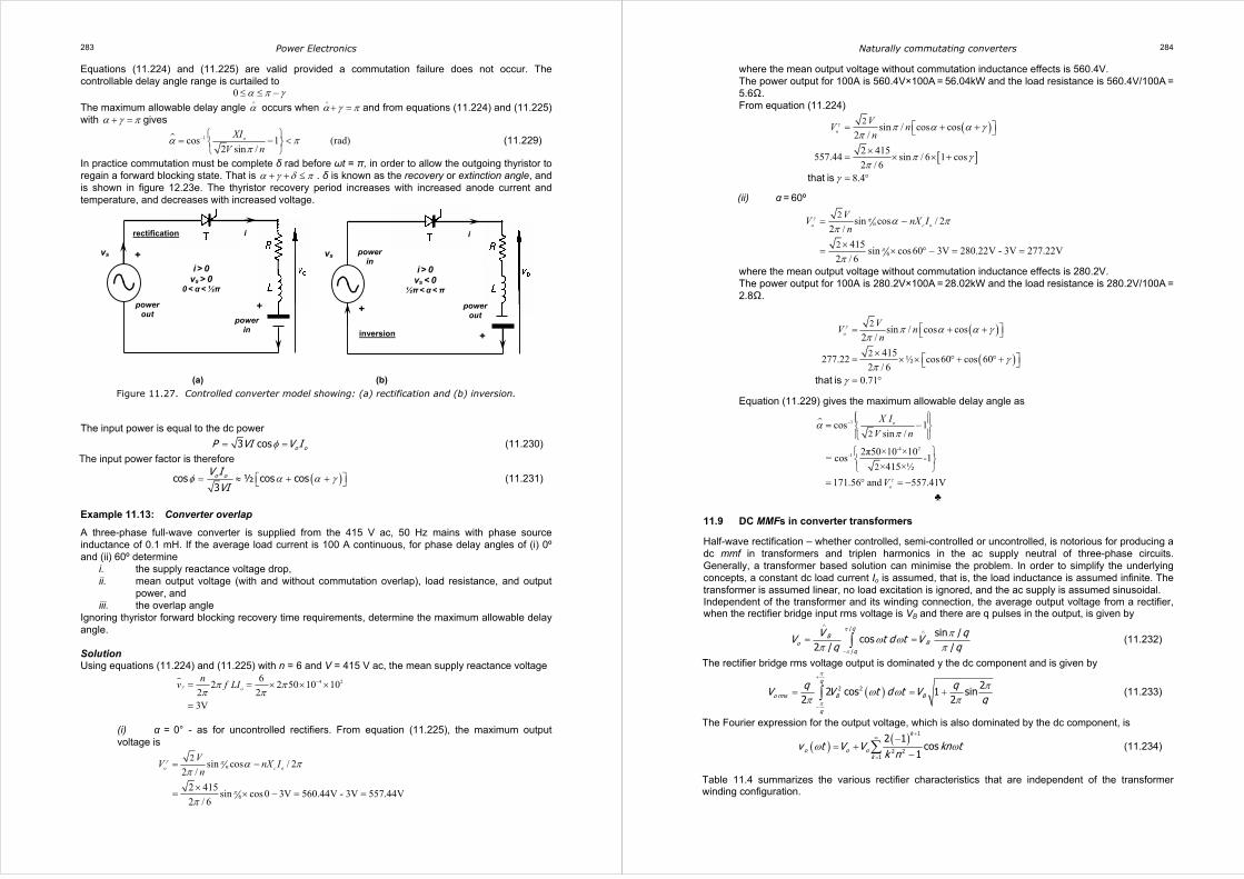
Power Electronics 283
i > 0 vs > 0
0 < α < ½π
i
vs +
+ +
i > 0 vs < 0
½π < α < π
i
vs
+
(a) (b)
power out
power in
power in
power out
rectification
inversion
Equations (11.224) and (11.225) are valid provided a commutation failure does not occur. The controllable delay angle range is curtailed to 0 α π γ≤ ≤ −
The maximum allowable delay angle α∧
occurs when α γ π∧+ = and from equations (11.224) and (11.225)
with α γ π+ = gives
1cos 1 (rad)2 sin /
oXI
V nα π
π− = − <
(11.229)
In practice commutation must be complete δ rad before ωt = π, in order to allow the outgoing thyristor to regain a forward blocking state. That is α γ δ π+ + ≤ . δ is known as the recovery or extinction angle, and is shown in figure 12.23e. The thyristor recovery period increases with increased anode current and temperature, and decreases with increased voltage.
Figure 11.27. Controlled converter model showing: (a) rectification and (b) inversion. The input power is equal to the dc power
3 cos o oP VI V Iφ= = (11.230)
The input power factor is therefore
( )cos ½ cos cos3o oV I
VIφ α α γ = ≈ + + (11.231)
Example 11.13: Converter overlap
A three-phase full-wave converter is supplied from the 415 V ac, 50 Hz mains with phase source inductance of 0.1 mH. If the average load current is 100 A continuous, for phase delay angles of (i) 0º and (ii) 60º determine
i. the supply reactance voltage drop, ii. mean output voltage (with and without commutation overlap), load resistance, and output
power, and iii. the overlap angle
Ignoring thyristor forward blocking recovery time requirements, determine the maximum allowable delay angle. Solution Using equations (11.224) and (11.225) with n = 6 and V = 415 V ac, the mean supply reactance voltage
4 262 2 50 10 10
2 23V
o
nv f LIγ π π
π π−= = × × ×
=
(i) α = 0° - as for uncontrolled rectifiers. From equation (11.225), the maximum output voltage is
6
2 sin cos / 22 /
2 415 sin cos 0 3V 560.44V - 3V 557.44V2 / 6
γ π
π
α ππ
π
= −
×= × − = =
o c onV
V nX In
Naturally commutating converters 284
where the mean output voltage without commutation inductance effects is 560.4V. The power output for 100A is 560.4V×100A = 56.04kW and the load resistance is 560.4V/100A =
5.6Ω. From equation (11.224)
( )
[ ]
2 sin / cos cos2 /
2 415557.44 sin / 6 1 cos2 / 6
8.4
o
VV n
nγ π α α γ
π
π γπ
γ
= + +
×= × × +
= °that is
(ii) α = 60º
6
2
2
sin cos / 22 /
415 sin cos 60 3V 280.22V - 3V 277.22V2 / 6
γ π
π
α ππ
π
= −
×= × ° − = =
o c onV
V nX In
where the mean output voltage without commutation inductance effects is 280.2V. The power output for 100A is 280.2V×100A = 28.02kW and the load resistance is 280.2V/100A =
2.8Ω.
( )
( )
2
2
sin / cos cos2 /
415277.22 ½ cos 60 cos 602 / 6
0.71
o
VV n
nγ π α α γ
π
γπ
γ
= + +
× = × × ° + ° +
= °that is
Equation (11.229) gives the maximum allowable delay angle as
1
-4 2-1
2
2
cos 1sin /
2π50×10 ×10= cos -1×415×½
171.56 and 557.41V
o
o
X I
V n
V γ
απ
− = −
= ° = −
♣ 11.9 DC MMFs in converter transformers Half-wave rectification – whether controlled, semi-controlled or uncontrolled, is notorious for producing a dc mmf in transformers and triplen harmonics in the ac supply neutral of three-phase circuits. Generally, a transformer based solution can minimise the problem. In order to simplify the underlying concepts, a constant dc load current Io is assumed, that is, the load inductance is assumed infinite. The transformer is assumed linear, no load excitation is ignored, and the ac supply is assumed sinusoidal. Independent of the transformer and its winding connection, the average output voltage from a rectifier, when the rectifier bridge input rms voltage is VB and there are q pulses in the output, is given by
/
/
sin /cos
2 / /
qB
Boq
V qV t d t V
q q
π
π
πω ωπ π
∧∧
−
= =∫ (11.232)
The rectifier bridge rms voltage output is dominated y the dc component and is given by
( )2 2 22 cos 1 sin
2 2
q
o rms B B
q
q qV V t d t Vq
π
π
πω ωπ π
+
−
= = +∫ (11.233)
The Fourier expression for the output voltage, which is also dominated by the dc component, is
( ) ( ) 1
2 21
2 1cos
1
k
o o ok
v t V V kn tk n
ω ω+
∞
=
−= +
−∑ (11.234)
Table 11.4 summarizes the various rectifier characteristics that are independent of the transformer winding configuration.
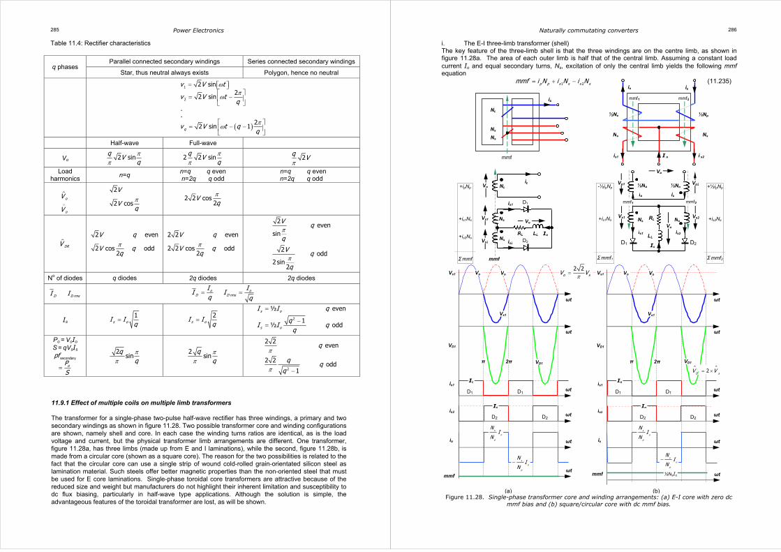
Power Electronics 285
Table 11.4: Rectifier characteristics
Parallel connected secondary windings Series connected secondary windings q phases
Star, thus neutral always exists Polygon, hence no neutral
( )
1
2
2 sin2
2 sin
.
.2
2 sin 1q
v V t
v V tq
v V t qq
ωπω
πω
=
= −
= − −
Half-wave Full-wave
Vo 2 sinq
Vqπ
π 2 2 sin
qV
qπ
π 2
q Vπ
Load harmonics
n=q n=q q even n=2q q odd
n=q q even n=2q q odd
o
o
V
V∨
2
2 cos
V
Vqπ 2 2 cos
2V
qπ
DRV
2 even
2 cos odd2
V q
V qqπ
2 2 even
2 2 cos odd2
V q
V qqπ
2 even
sin
2 odd
2sin2
V q
q
V q
q
π
π
No of diodes q diodes 2q diodes 2q diodes
D D rmsI I o oD D rms
I II I
q q= =
Is 1
s oI Iq
= 2
s oI Iq
= 2
½ even
1½ odd
s o
s o
I I q
qI I q
q
=
−=
Po = VoIo S = qVsIs
secondary
o
pfPS
=
2sin
qqπ
π
2sin
qqπ
π
2
2 2 even
2 2 odd
1
q
q qq
π
π −
11.9.1 Effect of multiple coils on multiple limb transformers The transformer for a single-phase two-pulse half-wave rectifier has three windings, a primary and two secondary windings as shown in figure 11.28. Two possible transformer core and winding configurations are shown, namely shell and core. In each case the winding turns ratios are identical, as is the load voltage and current, but the physical transformer limb arrangements are different. One transformer, figure 11.28a, has three limbs (made up from E and I laminations), while the second, figure 11.28b, is made from a circular core (shown as a square core). The reason for the two possibilities is related to the fact that the circular core can use a single strip of wound cold-rolled grain-orientated silicon steel as lamination material. Such steels offer better magnetic properties than the non-oriented steel that must be used for E core laminations. Single-phase toroidal core transformers are attractive because of the reduced size and weight but manufacturers do not highlight their inherent limitation and susceptibility to dc flux biasing, particularly in half-wave type applications. Although the solution is simple, the advantageous features of the toroidal transformer are lost, as will be shown.
Naturally commutating converters 286
(a) (b)
2 2o sV V
π=
Np
Ns
ip
Ns
+ipNp
+is1Ns
+is2Ns
Σ mmf mmf
is1
Io
Np
RL LL
Ns
Ns
Vp
Vs1
Vs2 is2
Vo
ip
D1 D2
mmf
is1
Vs1
is2
ωt
ip
ωt
ωt
ωt
ωt
Io
Io
s
o
p
NI
N
s
o
p
NI
N−
π 2π
D1 D1
D2 D2
VD1
Vs1
Vo
ωt
Vo
mmf is1 I o i s2
½Np
Ns
ip
Ns
ip
½Np
mmf1 mmf2
-½ipNp
+is1Ns
Σ mmf1
+½ipNp
+is2Ns
Σ mmf2
D1 D2
mmf
is1
Vs1
is2
ωt
ip
ωt
ωt
ωt
Io
Io
s
o
p
NI
N
s
o
p
NI
N−
π 2π
D1 D1
D2 D2
VD1
Vs1
Vo
ωt
Vo
ωt ½NsIo
2D s
V V= ×
mmf2 mmf1
Vp
Vo
Vs1 Vs2
Vp1 Vp2
is1
Io
½Np
LL
Ns Ns
is2
ip
RL
ip
½Np
VD1
VD1
i. The E-I three-limb transformer (shell) The key feature of the three-limb shell is that the three windings are on the centre limb, as shown in figure 11.28a. The area of each outer limb is half that of the central limb. Assuming a constant load current Io and equal secondary turns, Ns, excitation of only the central limb yields the following mmf equation 1 2p p s s s smmf i N i N i N= + − (11.235)
Figure 11.28. Single-phase transformer core and winding arrangements: (a) E-I core with zero dc
mmf bias and (b) square/circular core with dc mmf bias.
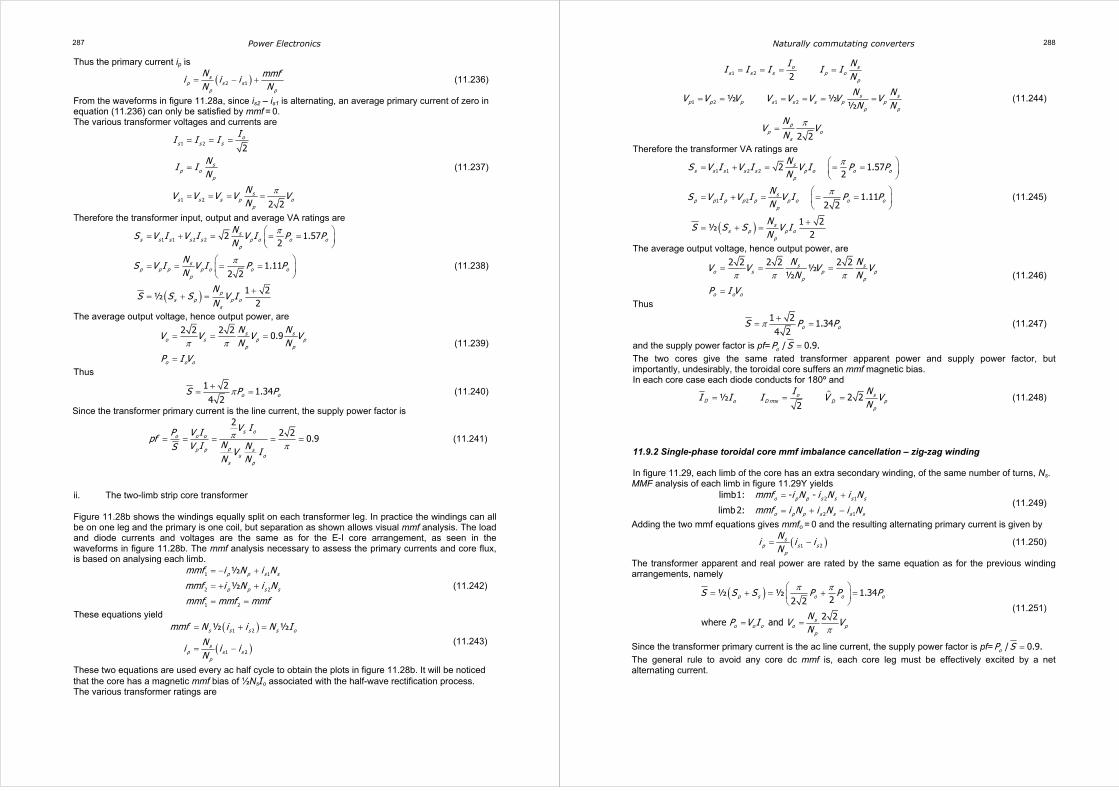
Power Electronics 287
Thus the primary current ip is
( )2 1s
p s sp p
N mmfi i i
N N= − + (11.236)
From the waveforms in figure 11.28a, since is2 – is1 is alternating, an average primary current of zero in equation (11.236) can only be satisfied by mmf = 0. The various transformer voltages and currents are
1 2
1 2
2
2 2
os s s
sp o
p
ss s s p o
p
II I I
NI I
N
NV V V V V
Nπ
= = =
=
= = = =
(11.237)
Therefore the transformer input, output and average VA ratings are
( )
1 1 2 2 2 1.572
1.112 2
1 2½
2
ss s s s s p o o o
p
sp p p p o o o
p
ps p p o
s
NS V I V I V I P P
N
NS V I V I P P
N
NS S S V I
N
π
π
= + = = =
= = = =
+= + =
(11.238)
The average output voltage, hence output power, are
2 2 2 20.9s s
o s p pp p
o o o
N NV V V V
N N
P I V
π π= = =
=
(11.239)
Thus
1 2
1.344 2
o oS P Pπ+= = (11.240)
Since the transformer primary current is the line current, the supply power factor is
22 2
0.9s o
o o o
pp p ss o
s p
V IP V Ipf
NV I NS V IN N
ππ
= = = = = (11.241)
ii. The two-limb strip core transformer Figure 11.28b shows the windings equally split on each transformer leg. In practice the windings can all be on one leg and the primary is one coil, but separation as shown allows visual mmf analysis. The load and diode currents and voltages are the same as for the E-I core arrangement, as seen in the waveforms in figure 11.28b. The mmf analysis necessary to assess the primary currents and core flux, is based on analysing each limb.
1 1
2 2
1 2
½
½p p s s
p p s s
mmf i N i N
mmf i N i N
mmf mmf mmf
= − +
= + +
= =
(11.242)
These equations yield
( )
( )
1 2
1 2
½ ½s s s s o
sp s s
p
mmf N i i N I
Ni i i
N
= + =
= − (11.243)
These two equations are used every ac half cycle to obtain the plots in figure 11.28b. It will be noticed that the core has a magnetic mmf bias of ½NsIo associated with the half-wave rectification process. The various transformer ratings are
Naturally commutating converters 288
1 2
1 2 1 2
2
½ ½½
2 2
o ss s s p o
p
s sp p p s s s p p
p p
pp o
s
I NI I I I I
N
N NV V V V V V V V
N N
NV V
Nπ
= = = =
= = = = = =
=
(11.244)
Therefore the transformer VA ratings are
( )
1 1 2 2
1 2
2 1.572
1.112 2
1 2½
2
ss s s s s p o o o
p
sp p p p p p o o o
p
ss p p o
p
NS V I V I V I P P
N
NS V I V I V I P P
N
NS S S V I
N
π
π
= + = = =
= + = = =
+= + =
(11.245)
The average output voltage, hence output power, are
2 2 2 2 2 2½
½s s
o s p pp p
o o o
N NV V V V
N N
P I V
π π π= = =
=
(11.246)
Thus
1 2
1.344 2
o oS P Pπ += = (11.247)
and the supply power factor is pf= / 0.9.oP S =
The two cores give the same rated transformer apparent power and supply power factor, but importantly, undesirably, the toroidal core suffers an mmf magnetic bias. In each core case each diode conducts for 180º and
½ 2 22o s
D o D rms pDp
I NI I I V V
N= = = (11.248)
11.9.2 Single-phase toroidal core mmf imbalance cancellation – zig-zag winding In figure 11.29, each limb of the core has an extra secondary winding, of the same number of turns, Ns. MMF analysis of each limb in figure 11.29Y yields
2 1
2 1
limb1: - -
limb2:o p p s s s s
o p p s s s s
mmf i N i N i N
mmf i N i N i N
= +
= + − (11.249)
Adding the two mmf equations gives mmfo = 0 and the resulting alternating primary current is given by
( )1 2s
p s sp
Ni i i
N= − (11.250)
The transformer apparent and real power are rated by the same equation as for the previous winding arrangements, namely
( )½ ½ 1.3422 2
2 2where and
p s o o o
so o o o p
p
S S S P P P
NP V I V V
N
π π
π
= + = + =
= =
(11.251)
Since the transformer primary current is the ac line current, the supply power factor is pf= / 0.9.oP S =
The general rule to avoid any core dc mmf is, each core leg must be effectively excited by a net alternating current.
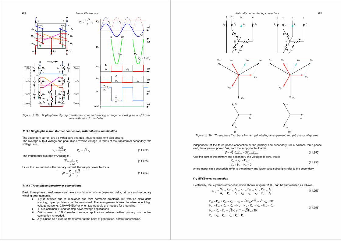
Power Electronics 289
Figure 11.29. Single-phase zig-zag transformer core and winding arrangement using square/circular
core with zero dc mmf bias. 11.9.3 Single-phase transformer connection, with full-wave rectification The secondary current are ac with a zero average , thus no core mmf bias occurs. The average output voltage and peak diode reverse voltage, in terms of the transformer secondary rms voltage, are
2 2
2o s Dr sV V V Vπ
= = (11.252)
The transformer average VAr rating is
2 2
oS Pπ= (11.253)
Since the line current is the primary current, the supply power factor is
2 2oP
pfS π
= = (11.254)
11.9.4 Three-phase transformer connections Basic three-phase transformers can have a combination of star (wye) and delta, primary and secondary winding arrangements.
i. Y-y is avoided due to imbalance and third harmonic problems, but with an extra delta winding, triplen problems can be minimised. The arrangement is used to interconnect high voltage networks, 240kV/345kV or when two neutrals are needed for grounding.
ii. Y- δ is commonly used for step-down voltage applications. iii. ∆-δ is used in 11kV medium voltage applications where neither primary nor neutral
connection is needed. iv. ∆-y is used as a step-up transformer at the point of generation, before transmission.
is1 I o i s2
Np
Ns
ip
Ns
ip
Np
mmfo mmfo
Ns Ns
D1 D2
mmf mmf
Vp
Vs1
Vp1
Vs1
Vs2
Vp2
Vs2
Np
ip ip
Np
Vo is1
Io
LL
Ns Ns
is2
RL Ns Ns
-ipNp
-is2Ns
+is1Ns
Σmmfo
+ipNp
-is1Ns
+is2Ns
Σmmfo
mmf
ip ωt
s
o
p
NI
N
s
o
p
NI
N−
ωto
D1 D1
D2 D2
is1
is2
ωt
ωt
Io
Io
ωt
VD1
VD1
4D s
V V= ×
VD1
Vs1
ωt
π 2π
Vo Vo
Vs1
4 2o sV V
π=
Naturally commutating converters 290
VBN
IB IC IN IA
B C N A
N
Ib Ic In Ia
b c n a
n
Vbn
IC
IB
IA
Ic
Ib
Ia
VBN
VCN
VAN
VAB VCA
VBC
-VBN
Vbn
Vcn
Van
Vab Vca
Vbc
-Vbn
(a) (b)
Figure 11.30. Three-phase Y-y transformer: (a) winding arrangement and (b) phasor diagrams. Independent of the three-phase connection of the primary and secondary, for a balance three-phase load, the apparent power, VA, from the supply to the load is
3 3line line phase phaseS V I V I= = (11.255)
Also the sum of the primary and secondary line voltages is zero, that is
0
0AB BC CA
ab bc ca
V V VV V V
+ + =
+ + = (11.256)
where upper case subscripts refer to the primary and lower case subscripts refer to the secondary. Y-y (WYE-wye) connection Electrically, the Y-y transformer connection shown in figure 11.30, can be summarized as follows.
1
p a a b CN cAN BNY y
s an A L bn B cn C
N I I I V IV VN V I I V I V I
η − = = = = = = = = (11.257)
30
30
3 3 30
3 3 30
jAB AN NB AN BN AN AN
BC BN NC BN CN CA CN NA CN AN
jab an bn an an
bc bn cn ca cn an
V V V V V V e VV V V V V V V V V V
V V V V e VV V V V V V
°
°
= + = − = = ∠ °
= + = − = + = −
= − = = ∠ °
= − = −
(11.258)
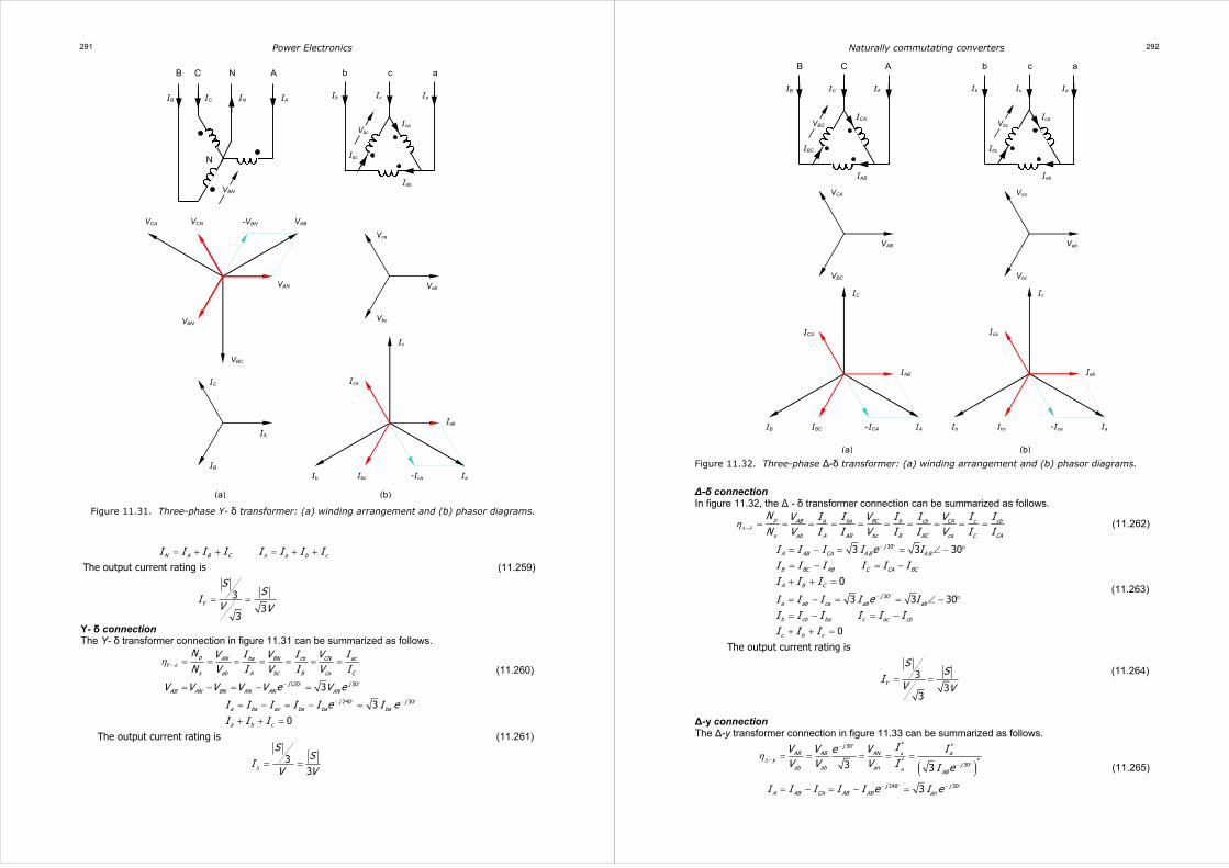
Power Electronics 291
Figure 11.31. Three-phase Y- δ transformer: (a) winding arrangement and (b) phasor diagrams.
The output current rating is
33
3
N A B C n a b c
Y
I I I I I I I I
SS
IV V
= + + = + +
= =
(11.259)
Y- δ connection The Y- δ transformer connection in figure 11.31 can be summarized as follows.
120 303
p ba cb CN acAN BNY
s ab A bc B ca C
j jAB AN BN AN AN AN
N I I V IV VN V I V I V I
V V V V V e V e
δη −
− ° °
= = = = = = =
= − = − =
(11.260)
240 303
0
The output current rating is
33
j ja ba ac ba ba ba
a b c
I I I I I e I eI I I
SS
IV V
− ° − °
∆
= − = − =
+ + =
= =
(11.261)
(a) (b)
Vbc
Ib Ic Ia
b c a
Ica
Iab
Ibc
VBN
IB IC IN IA
B C N A
N
Vca
Vbc
Vab
Ica
Ibc
Iab
IaIb
Ic
-Ica
IC
IB
IA
VBN
VCN
VAN
VAB VCA
VBC
-VBN
Naturally commutating converters 292
Figure 11.32. Three-phase ∆-δ transformer: (a) winding arrangement and (b) phasor diagrams. ∆-δ connection In figure 11.32, the ∆ - δ transformer connection can be summarized as follows.
p a ba BC b cb CA c cbAB
s ab A AB bc B BC ca C CA
N I I V I I V I IVN V I I V I I V I Iδη∆− = = = = = = = = = = (11.262)
30
30
3 3 30
0
3 3 30
0
jA AB CA A B A B
B BC AB C CA BC
A B C
ja ab ca ab ab
b cb ba c ac cb
c b c
I I I I e II I I I I II I I
I I I I e II I I I I II I I
− °
− °
= − = = ∠ − °
= − = −
+ + =
= − = = ∠ − °
= − = −
+ + =
(11.263)
The output current rating is
33
3Y
SS
IV V
= = (11.264)
∆-y connection The ∆-y transformer connection in figure 11.33 can be summarized as follows.
( )* *30
* *30
240 30
3 3
3
a
A
jaAB AB AN
yjab ab an
AB
j jA AB CA AB AB an
I IV V VeV V V I I e
I I I I I e I e
η− °
∆−− °
− ° − °
= = = = =
= − = − =
(11.265)
(a) (b)
VCA
VBC
VAB
ICA
IBC
IAB
IA IB
IC
-ICA
Vca
Vbc
Vab
Ica
Ibc
Iab
Ia Ib
Ic
-Ica
VBC
IB IC IA
B C A
ICA
IAB
IBC
Vbc
Ib Ic Ia
b c a
Ica
Iab
Ibc

Power Electronics 293
The output current rating is
33
3Y
SS
IV V
= = (11.266)
Figure 11.33. Three-phase ∆-y transformer: (a) winding arrangement and (b) phasor diagrams. 11.9.5 Three-phase transformer, half-wave rectifiers - core mmf imbalance Note that a delta secondary connection cannot be used for half-wave rectification as no physical neutral connection exists. i. star connected primary Y-y The three-phase half-wave rectifier with a star-star connected transformer in figure 11.34a is prone to magnetic mmf core bias. With a constant load current Io, each diode conducts for 120º. Each leg is analysed on an mmf basis, and the current and mmf waveforms in figure 11.34a are derived as follows.
1 1
2 2
3 3
o s s p p
o s s p p
o s s p p
mmf N i N i
mmf N i N i
mmf N i N i
= −
= −
= −
(11.267)
By symmetry and balance, the mmf in each leg must be equal.
(a) (b)
VBC
IB IC IA
B C A
ICA
IAB
IBC
Ib Ic In Ia
b c n a
n
Vbn
VCA
VBC
VAB
ICA
IBC
IAB
IA IB
IC
-ICA
Ic
Ib
Ia
Vbn
Vcn
Van
Vab Vca
Naturally commutating converters 294
If iN is the neutral current then the equation for the currents is 1 2 3p p p Ni i i i+ + = (11.268)
The same mmf equations are obtained if the load is purely resistive. Any triplens in the primary will add algebraically, while any other harmonics will vectorially cancel to zero. Therefore the neutral may only conduct primary side triplen currents. Any input current harmonics are due to the rectifier and the rectifier harmonics of the order h = cp±1 where c = 0,1,2,… and p is the pulse number, 3. No secondary-side third harmonics can exist hence h ≠ 3k for k = 1, 2, 3, . Therefore no primary-side triplen harmonic currents exist to flow in the neutral, that is iN = 0. In a balanced load condition, the neutral connection is redundant. The system equations resolve to
1 1 2 3
2 1 2 3
3 1 2 3
1 2 3
2 1 13 3 3
1 2 13 3 3
1 1 23 3 3
133
sp s s s
p
sp s s s
p
sp s s s
p
s s so s s o
Ni i i i
N
Ni i i i
N
Ni i i i
N
i i immf N N I
= − −
= − + −
= − − +
+ + = =
(11.269)
Specifically, the core has an mmf dc bias of NsIo. Waveforms satisfying these equations are show plotted in figure 11.34a. The various transformer currents and voltages are
1 2 3
1 2 3
1 2 3
1 2 3
3
23
2
3 62
1.173 6
os s s s
sp p p p o
p
pp p p p o
s
os s s s o
II I I I
NI I I I I
N
NV V V V V
NV
V V V V V
π
π
= = = =
= = = =
= = = =
= = = = =
(11.270)
Therefore the various transformer VA ratings are
( )
1 1 2 2 3 3
1 2 3
23 1.48
32
3 1.213 3
2 6½ 1.34
3 3
s s s s s s s s s o o
p p p p p p p p p o o
s p o o
S V I V I V I V I P P
S V I V I V I V I P P
S S S P P
π
π
= + + = = =
= + + = = =
+= + = =
(11.271)
The average output power is o o oP I V= (11.272)
Since with a wye connected transformer primary, the transformer primary phase current is the line current, the supply power factor is
3 32
2 0.8273 3
32
s oo o o
pp p ss o
s p
V IP V Ipf
NV I NS V IN N
π= = = = (11.273)
Although the neutral connection is redundant for a constant load current, the situation is different if the load current has ripple at the three times the rectified ac frequency, as with a resistive load. Equations in (11.269) remain valid for the untapped neutral case. In such a case, when triplens exist in the load current, how they are reflected into the primary depends on whether or not the neutral is connected:
• No neutral connection – a triplen mmf is superimposed on the mmf dc bias of ⅓NsIo. • Neutral connected – a dc current (zero sequence) flows in the neutral and the
associated zero sequence line currents in the primary, oppose the generation of any triplen mmf onto the dc mmf bias of ⅓NsIo.
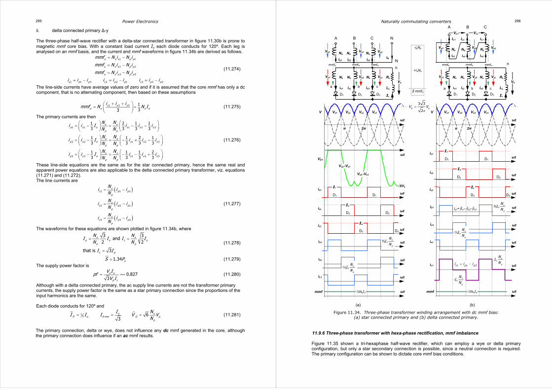
Power Electronics 295
ii. delta connected primary ∆-y The three-phase half-wave rectifier with a delta-star connected transformer in figure 11.30b is prone to magnetic mmf core bias. With a constant load current Io each diode conducts for 120º. Each leg is analysed on an mmf basis, and the current and mmf waveforms in figure 11.34b are derived as follows.
1 1
2 2
3 3
1 1 3 2 2 1 3 3 2
o s s p p
o s s p p
o s s p p
L p p L p p L p p
mmf N i N i
mmf N i N i
mmf N i N i
i i i i i i i i i
= −
= −
= −
= − = − = −
(11.274)
The line-side currents have average values of zero and if it is assumed that the core mmf has only a dc component, that is no alternating component, then based on these assumptions
1 2 3 133
s s so s s o
i i immf N N I
+ + = =
(11.275)
The primary currents are then
1 1 1 2 3
2 2 1 2 3
3 3 1 2 3
1 2 1 13 3 3 3
1 1 2 13 3 3 3
1 1 1 23 3 3 3
s sp s o s s s
p p
s sp s o s s s
p p
s sp s o s s s
p p
N Ni i I i i i
N N
N Ni i I i i i
N N
N Ni i I i i i
N N
= − = − −
= − = − + −
= − = − − +
(11.276)
These line-side equations are the same as for the star connected primary, hence the same real and apparent power equations are also applicable to the delta connected primary transformer, viz. equations (11.271) and (11.272). The line currents are
( )
( )
( )
1 1 3
2 2 1
3 3 2
sL p p
p
sL p p
p
sL p p
p
Ni i i
N
Ni i i
N
Ni i i
N
= −
= −
= −
(11.277)
The waveforms for these equations are shown plotted in figure 11.34b, where
3 3 and
2 2
that is 3
s sp o L o
p p
L p
N NI I I I
N N
I I
= =
=
(11.278)
1.34 oS P= (11.279)
The supply power factor is
0.8273
o o
p L
V Ipf
V I= == (11.280)
Although with a delta connected primary, the ac supply line currents are not the transformer primary currents, the supply power factor is the same as a star primary connection since the proportions of the input harmonics are the same. Each diode conducts for 120º and
13 6
3o s
D Do D rms pp
I NI I I V V
N= = = (11.281)
The primary connection, delta or wye, does not influence any dc mmf generated in the core, although the primary connection does influence if an ac mmf results.
Naturally commutating converters 296
Figure 11.34. Three-phase transformer winding arrangement with dc mmf bias: (a) star connected primary and (b) delta connected primary.
11.9.6 Three-phase transformer with hexa-phase rectification, mmf imbalance Figure 11.35 shown a tri-hexaphase half-wave rectifier, which can employ a wye or delta primary configuration, but only a star secondary connection is possible, since a neutral connection is required. The primary configuration can be shown to dictate core mmf bias conditions.
is1
Io
Np
LL
NsNs
is3
ip1
RL
ip3
Np Np
Ns
is2
ip2 iN
Vo
Vp1 Vp3 Vp2
Vs1 Vs3 Vs2
mmfo mmfo mmfo
A B C N
a b c
N
n
D1 D2 D3
is1
Io
LL
NsNs
is3
RL Ns
is2
Vo
Vs1 Vs3 Vs2
Np
ip1 ip3
Np Np
ip2
IL1 IL3 IL2
mmfo mmfo mmfo
Vp1 Vp3 Vp2
VL1 VL2
A B C
a b c
n
D1 D2 D3
mmf ωt ⅓NsIo
ip3 ωt
ip1 ωt ⅔Ios
p
N
N
ip2 ωt
-⅓Ios
p
N
N
is1 ωt
Io
is2 ωt
Io
is3 ωt
Io
IL1 ωt
-Ios
p
N
N
Ios
p
N
N
ωt
Vs1 Vs2 Vs3 Vs1
π 2π
V
D1 D1
D3 D3
D2 D2
3 3
2o sV V
π=
mmf ωt ⅓NsIo
ip3 ωt
ip1 ωt ⅔Ios
p
N
N
ip2 ωt
-⅓Ios
p
N
N
is1 ωt
Io
is2 ωt
Io
is3 ωt
Io
ωt
ωt
Vs1 Vs2 Vs3 Vs1
π 2π
V
D1 D1
D2 D2
D3 D3
VD1
Vs2 -Vs1
Vs3 -Vs1
√6Vs
-ipNp
+isNs
Σ mmfo
1 1 3L p pi i i= −
ip1=is1-is2-is3
(a) (b)
Power Electronics 297
i. Y-y connection The mmf balance for the wye primary connection in figure 11.35a is
1 4 1
3 6 2
5 2 3
1 2 3
0
0
0
0
s s s s p p
s s s s p p
s s s s p p
p p p
N i N i N i
N i N i N i
N i N i N i
i i i
− − =
− − =
− − =
+ + =
(11.282)
The primary currents expressed in terms of the secondary current are
( )
( )
( )
( )
1 1 2 3 4 5 6
2 1 2 3 4 5 6
3 1 2 3 4 5 6
1 2 3 4 5 6
2 1 1 2 1 13 3 3 3 3 3
1 1 2 1 1 23 3 3 3 3 3
1 2 1 1 2 13 3 3 3 3 3
13
sp s s s s s s
p
sp s s s s s s
p
sp s s s s s s
p
s s s s s s s
Ni i i i i i i
NN
i i i i i i iNN
i i i i i i iN
mmf N i i i i i i
= + − − − +
= − + + + − −
= − − − + − −
= − + − + −
(11.283)
These line side equations are plotted in figure 11.35a. Notice that an alternating mmf exists in the core related to the pulse frequency, n = 2q = 6. The transformer primary currents and the line currents are
23
23
p o
L o
i I
i I
=
=
(11.284)
Note that because of the zero sequence current, triplens, in the delta primary that
2
not
3
L p
L p
i i
i i
=
=
(11.285)
The transformer power ratings are
( )
16
3 2 6 3
23
3 33 2
½ 3 1 1.433 63
s o o o
p o o o
o o o o
S V I P
S V I P
S P P P P
π π
π π
π π π
= =
= =
= + = + =
(11.286)
i. ∆-y connection When the primary is delta connected, as shown in figure 11.35b, the mmf equations are the same as with a wye primary, namely
1 4 1
3 6 2
5 2 3
0
0
0
s s s s p p
s s s s p p
s s s s p p
N i N i N i
N i N i N i
N i N i N i
− − =
− − =
− − =
(11.287)
but Kirchhoff’s electrical current equation becomes of the following form for each phase:
( )2
1 40
10
2 s s smmf N i i d tπ
ωπ
= − =∫ (11.288)
Thus since each limb experiences an alternating current, similar to is1-is4 for each limb, with an average value of zero, the line currents can be calculated from
( ) ( ) ( )1 1 4 2 3 6 3 5 2s s s
p s s p s s p s sp p p
N N Ni i i i i i i i i
N N N= − = − = − (11.289)
Naturally commutating converters 298
The line currents are
( )
( )
( )
1 1 3 1 2 4 5
2 2 1 1 3 4 6
3 3 2 2 3 5 6
sL p p s s s s
p
sL p p s s s s
p
sL p p s s s s
p
Ni i i i i i i
N
Ni i i i i i i
N
Ni i i i i i i
N
= − = + − −
= − = − + + −
= − = − − + +
(11.290)
The transformer primary currents and the line currents are
1
3
23
p o
L o
i I
i I
=
=
(11.291)
The transformer power ratings are
63 2 6 3
33 2 3 6
1½ ½ 1 1.54
3 6 3 2
os o o
op o o
o o o o
IS V P
IS V P
S P P P P
π π
π π
π π π
= =
= =
= + = + =
(11.292)
The supply power factor is pf = 3/π = 0.955. Independent of the primary connection, the average output voltage is
3 2
1.35o s sV V Vπ
= = (11.293)
and the diode average and rms currents are
6 6o o
D D rms
I II I= = (11.294)
The maximum diode reverse voltage is
2 2Dr sV V= (11.295)
The line currents are added to the waveforms in figure 11.35a and are also shown in figure 11.35b. The core mmf bias is zero, without any ac component associated with the 6 pulse rectification process. Zero sequence, triplen currents, can flow in the delta primary connection. A star connected primary is therefore not advisable.
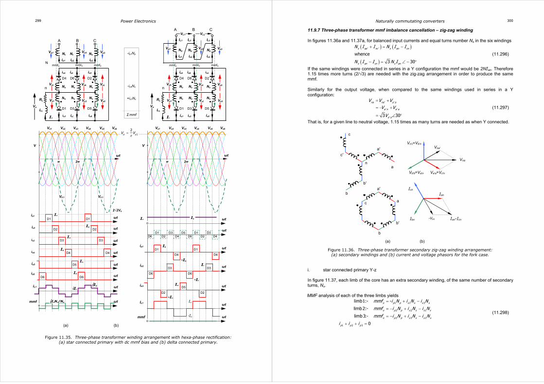
Power Electronics 299
Figure 11.35. Three-phase transformer winding arrangement with hexa-phase rectification: (a) star connected primary with dc mmf bias and (b) delta connected primary.
(a) (b)
1
2o sV V
π=
-ip1Np
-is4Ns
+is1Ns
Σ mmf
A B C
mmfo mmfo mmfo
Np
ip1 ip3
Np Np
ip2
Vp1 Vp3Vp2
N
NsNs Ns
NsNs Ns
is1 is5 is3
Vs1 Vs5 Vs3
Io
LL
RL
Vo D1 D3 D5
n
is4 is2 is6
D4 D6 D2
Vs4 Vs2 Vs6
NsNs Ns
NsNs Ns
is1 is5 is3
Vs1 Vs5 Vs3
Io
LL
RL
Vo D1 D3 D5
n
is4 is2is6
D4 D6 D2
Vs4 Vs2 Vs6
mmfo mmfo mmfo
Np
ip1 ip3
Np Np
ip2
IL1 IL3 IL2
Vp1 Vp3 Vp2
VL1 VL2
A B C
D1 D1
D4 D4
D3 D3
D6 D6
D5
D2 D2
ip1 Io
-Io
ip2 Io
-Io
ip3 Io
-Io
ωt
ωt
ωt
Io ωt o
Io
mmf ωt o
D1 D3 D5 D1 D3 ωt
D6 D2 D4 D6 D2 D4
Io
-Io
IL1 ωt
π 2π
V
Vs1 Vs2 Vs3 Vs4 Vs5 Vs6
ωtωt
π 2π
V
VD1 VD1
2√2Vs
Vs1 Vs2 Vs3 Vs4 Vs5 Vs6
Io Io
iL1 ωt
D4 D4 Io is4 ωt
D5 is5 ωt Io
is6 ωt D6 D6 Io
is3 ωt D3 D3 Io
is2 ωt D2 D2 Io
is1 ωt D1 D1 Io
mmf ωt IoNs/Np o
Naturally commutating converters 300
11.9.7 Three-phase transformer mmf imbalance cancellation – zig-zag winding In figures 11.36a and 11.37a, for balanced input currents and equal turns number Ns in the six windings
( ) ( )
( )
' '
whence
3 30
s aa nc s an cn
s an cn s an
N I I N I I
N I I N I
+ = −
− = ∠ − °
(11.296)
If the same windings were connected in series in a Y configuration the mmf would be 2NIan. Therefore 1.15 times more turns (2/√3) are needed with the zig-zag arrangement in order to produce the same mmf. Similarly for the output voltage, when compared to the same windings used in series in a Y configuration:
' '
' '
'3 30
na na a a
a n a a
a a
V V VV V
V
= +
= − +
= ∠ °
(11.297)
That is, for a given line to neutral voltage, 1.15 times as many turns are needed as when Y connected.
Figure 11.36. Three-phase transformer secondary zig-zag winding arrangement: (a) secondary windings and (b) current and voltage phasors for the fork case.
i. star connected primary Y-z In figure 11.37, each limb of the core has an extra secondary winding, of the same number of secondary turns, Ns. MMF analysis of each of the three limbs yields
1 1 3
2 2 1
2 3 2
1 2 3
limb1:- -
limb2:-
limb3:-
0
o p p s s s s
o p p s s s s
o p p s s s s
p p p
mmf i N i N i N
mmf i N i N i N
mmf i N i N i N
i i i
= + −
= − + −
= − + −
+ + =
(11.298)
(a) (b)
Vna
Va′a=Vc′n Vb′b=Va′n
Vna′ Vc′c=Vb′n
Ian-Icn
Ian Icn
Ibn -Vbn
a
b
a′
b′
c′
c
n
b
b′
a
a′
c

Power Electronics 301
Adding the three mmf equations gives mmfo = 0 and the alternating primary (and line) currents are
( )
( )
( )
1 1 3
2 2 1
3 3 2
sp s s
p
sp s s
p
sp s s
p
Ni i i
N
Ni i i
N
Ni i i
N
= −
= −
= −
(11.299)
These equations are plotted in figure 11.37a. If a 1:1:1 turns ratio is assumed, the power ratings of the transformer (which is independent of the turns ratio) involves the vectorial addition of the winding voltages.
1 11 2
2 21 3
3 31 1
s s s o
s s s o
s s s o
v v v
v v v
v v v
= −
= −
= −
(11.300)
The various transformer ratings are (11.301)
( ) ( )
0 1
2 2 23 3 6 3
3 3 3 3
½ 2 1 1.463 3
s s s s s s so o p p p o
s p o o
S I V I V I V P S I V P
S S S P P
π π
π
= + = = = =
= + = + =
(11.302)
ii. delta connected primary ∆-z Carrying out an mmf balancing exercise, assuming no alternating mmf component, and the mean line current is zero, yields
( )
( )
( )
1 1 3 1 2 3
2 2 1 2 3 1
3 3 2 3 1 2
2
2
2
sL p p s s s
p
sL p p s s s
p
sL p p s s s
p
Ni i i i i i
N
Ni i i i i i
N
Ni i i i i i
N
= − = + −
= − = + −
= − = + −
(11.303)
The primary and secondary currents are the same whether for a delta or star connected primary, therefore
( )½ 1.46s p oS S S P= + = (11.304)
If a 1:1:1 turns ratio is assumed, the line, primary and load current are related according to
2 22 42
3 3
23
3
L o o o
p o L p
I I I I
I I I I
= + =
= =
(11.305)
A zig-zag secondary can be a Y-type fork for a possible neutral connection or alternatively, a ∆-type polygon when the neutral is not required. Each diode conducts for 120º and
13 6
3o s
D Do D rms pp
I NI I I V V
N= = = (11.306)
Naturally commutating converters 302
Figure 11.37. Three-phase transformer winding zig-zag arrangement with no dc mmf bias:
(a) star connected primary and (b) delta connected primary.
mmfo mmfo mmfo
Np
ip1 ip3
Np Np
ip2
Vp1 Vp3 Vp2
Vs1o Vs3o Vs2o
Vs11 Vs31 Vs21
Vs1
is1
Io
LL
Ns Ns
is3
RL Ns
is2
Ns Ns Ns
Vo
A B C
a b c
n
D1 D2 D3
N
mmf ωt o
is1 ωt
Io
is2 ωt
Io
is3 ωt
Io
ip1 ωt Io
s
p
N
N
-Io
s
p
N
N ip2 ωt Io
s
p
N
N
-Io
s
p
N
N ip3 ωt Io
s
p
N
N
-Io
s
p
N
N
ωt
ωt
Vs1 Vs2 Vs3 Vs1
π 2π
V
VD1
Vs2 -Vs1
Vs3 -Vs1
√6Vs
Vs11 Vs21
Vs31
-Vs3o
Vs2
-ip1Np
-is3Ns
+is1Ns
Σmmfo
1
3 3
2o sV V
π=
Np
ip1 ip3
Np Np
ip2
IL1 IL3 IL2
mmfo mmfo mmfo
Vp1 Vp3 Vp2
VL1 VL2
is1
Io
LL
NsNs
is3
RL Ns
is2
Ns Ns Ns
Vo
Vs1o Vs3o Vs2o
Vs11 Vs31 Vs21
Vs1
A B C
a b c
n
D1 D2 D3
N
is1 ωt
Io
is2 ωt
Io
is3 ωt
Io
mmf ωt o
iL2 ωt Io
s
p
N
N
-2Io
s
p
N
N
iL1 ωt
-2Io
s
p
N
N
Io
s
p
N
N
ip1 ωt Io
s
p
N
N
-Io
s
p
N
N
ωt
Vs1 Vs2 Vs3 Vs1
π 2π
V
ωt
VCB VBA VAC VCB
π 2π
VL-L
D1 D1
D2 D2
D3
D1 D1
D2 D2
D3
(a) (b)
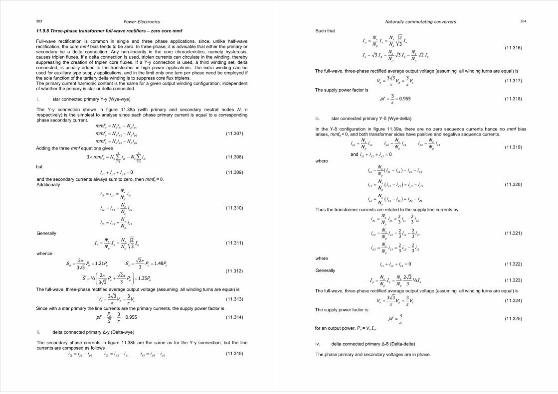
Power Electronics 303
11.9.8 Three-phase transformer full-wave rectifiers – zero core mmf Full-wave rectification is common in single and three phase applications, since, unlike half-wave rectification, the core mmf bias tends to be zero. In three-phase, it is advisable that either the primary or secondary be a delta connection. Any non-linearity in the core characteristics, namely hysteresis, causes triplen fluxes. If a delta connection is used, triplen currents can circulate in the winding, thereby suppressing the creation of triplen core fluxes. If a Y-y connection is used, a third winding set, delta connected, is usually added to the transformer in high power applications. The extra winding can be used for auxiliary type supply applications, and in the limit only one turn per phase need be employed if the sole function of the tertiary delta winding is to suppress core flux triplens. The primary current harmonic content is the same for a given output winding configuration, independent of whether the primary is star or delta connected. i. star connected primary Y-y (Wye-wye) The Y-y connection shown in figure 11.38a (with primary and secondary neutral nodes N, n respectively) is the simplest to analyse since each phase primary current is equal to a corresponding phase secondary current.
1 1
2 2
2 2
o s s p p
o s s p p
o s s p p
mmf N i N i
mmf N i N i
mmf N i N i
= −
= −
= −
(11.307)
Adding the three mmf equations gives
3 3
1 1
3 o p pi s sii i
mmf N i N i= =
× = −∑ ∑ (11.308)
but 1 2 3 0p p pi i i+ + = (11.309)
and the secondary currents always sum to zero, then mmfo = 0. Additionally
1 1 1
2 2 2
3 3 3
sL p s
p
sL p s
p
sL p s
p
Ni i i
N
Ni i i
N
Ni i i
N
= =
= =
= =
(11.310)
Generally
23
s sp s o
p p
N NI I I
N N= = (11.311)
whence
2 21.21 1.48
33 3
2 2½ 1.35
33 3
p o o s o o
o o o
S P P S P P
S P P P
π π
π π
= = = =
= + =
(11.312)
The full-wave, three-phase rectified average output voltage (assuming all winding turns are equal) is
3 3 3
o p LV V Vπ π
= = (11.313)
Since with a star primary the line currents are the primary currents, the supply power factor is
3
0.955oPpf
S π= = = (11.314)
ii. delta connected primary ∆-y (Delta-wye) The secondary phase currents in figure 11.38b are the same as for the Y-y connection, but the line currents are composed as follows 1 1 3 2 2 1 3 3 2L p p L p p L p pi i i i i i i i i= − = − = − (11.315)
Naturally commutating converters 304
Such that
23
3 3 2
s sp s o
p p
s sL p s o
p p
N NI I I
N N
N NI I I I
N N
= =
= = =
(11.316)
The full-wave, three-phase rectified average output voltage (assuming all winding turns are equal) is
3 3 3
o p LV V Vπ π
= = (11.317)
The supply power factor is
3
0.955pfπ
= = (11.318)
iii. star connected primary Y-δ (Wye-delta) In the Y-δ configuration in figure 11.39a, there are no zero sequence currents hence no mmf bias arises, mmfo = 0, and both transformer sides have positive and negative sequence currents.
1 1 2 2 3 3
1 2 3and 0
s s sp s p s p s
p p p
s s s
N N Ni i i i i i
N N N
i i i
= = =
+ + =
(11.319)
where
( )
( )
( )
1 1 2 1 2
2 2 3 2 3
2 3 1 3 1
sL s s p p
p
sL s s p p
p
sL s s p p
p
Ni i i i i
N
Ni i i i i
N
Ni i i i i
N
= − = −
= − = −
= − = −
(11.320)
Thus the transformer currents are related to the supply line currents by
1 1 1 2
2 2 2 3
3 3 3 1
2 23 3
2 23 3
2 23 3
sp s L L
p
sp s L L
p
sp s L L
p
Ni i i i
N
Ni i i i
N
Ni i i i
N
= = −
= = −
= = −
(11.321)
where 1 2 3 0L L Li i i+ + = (11.322)
Generally
2 2
½3
s sp s o
p p
N NI I I
N N= = (11.323)
The full-wave, three-phase rectified average output voltage (assuming all winding turns are equal) is
3 3 3
o p LV V Vπ π
= = (11.324)
The supply power factor is
3
pfπ
= (11.325)
for an output power, Po = Vo Io, iv. delta connected primary ∆-δ (Delta-delta) The phase primary and secondary voltages are in phase.
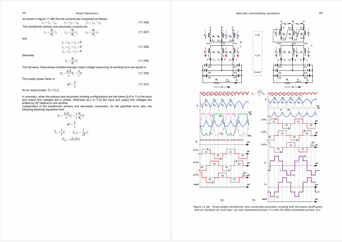
Power Electronics 305
As shown in figure 11.39b the line currents are composed as follows 1 1 3 2 2 1 3 3 2L p p L p p L p pi i i i i i i i i= − = − = − (11.326)
The transformer primary and secondary currents are
1 1 2 2 3 3s s s
p s p s p sp p p
N N Ni i i i i i
N N N= = = (11.327)
and
1 2 3
1 2 3
1 2 3
0
0
0
p p p
s s s
L L L
i i i
i i ii i i
+ + =
+ + =
+ + =
(11.328)
Generally
sp s
p
NI I
N= (11.329)
The full-wave, three-phase rectified average output voltage (assuming all winding turns are equal) is
3 3 3
o p LV V Vπ π
= = (11.330)
The supply power factor is
3pfπ
= (11.331)
for an output power, Po = Vo Io, In summary, when the primary and secondary winding configurations are the same (∆-δ or Y-y) the input and output line voltages are in phase, otherwise (∆-y or Y-δ) the input and output line voltages are shifted by 30º relative to one another. Independent of the transformer primary and secondary connection, for the specified turns ratio, the following electrical equations hold.
3 3 3
3
1 13 3
3 2
so p L
p
D o D rms o
DR s
NV V V
N
pf
I I I I
V V
π π
π
= =
=
= =
=
Naturally commutating converters 306
Figure 11.38. Three-phase transformer wye connected secondary winding with full-wave rectification and no resultant dc mmf bias: (a) star connected primary Y-y and (b) delta connected primary ∆-y.
is1
NsNs
is3
Ns
is2
Vs1 Vs3 Vs2
IoLL RL
Vo
mmfo mmfo mmfo
Np
ip1 ip3
Np Np
ip2
Vp1 Vp3 Vp2
A B C
a b c
N
n
D4 D1
D6 D3
D2 D5
Np
ip1 ip3
Np Np
ip2
IL1 IL3 IL2
mmfo mmfo mmfo
Vp1 Vp3 Vp2
VL1 VL2
is1
NsNs
is3
Ns
is2
Vs1 Vs3 Vs2
IoLL RL
Vo
A B C
a b c
n
D4 D1
D6 D3
D2 D5
-ip1Np
+is1Ns
Σ mmf
1
3 3o sV V
π=
mmf ωt o
Io ωt o
Io
ip1=is1 ωt Io
-Io
ip2=is2 ωt Io
-Io
ip1=is3 ωt Io
-Io
D1 D1
D4 D4
D3 D3
D6 D6
D5 D5
D2 D2
ac ba cb ac ab bc ca ab
ωt
π 2π
V Vs1 Vs2 Vs3 Vs1
VD4 VD1
Van Vbn Vcn Van
√6Vs
iL1 ωt
iL2 ωt
Io 2Io
-Io
Io
-2Io
-2Io
ip1=is1 ωt Io
-Io
ip2=is2 ωt Io
-Io
ip1=is3 ωt Io
-Io
D1 D1
D4 D4
D3 D3
D6 D6
D5 D5
D2 D2
ac ba cb ac ab bc ca ab
ωt
π 2π
V Vs1 Vs2 Vs3 Vs1
Van Vbn Vcn Van
mmf ωt o
(a) (b)
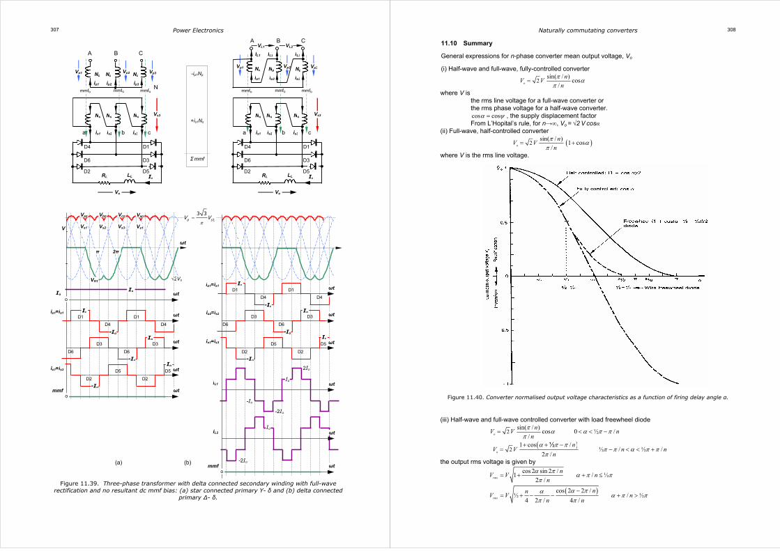
Power Electronics 307
Figure 11.39. Three-phase transformer with delta connected secondary winding with full-wave rectification and no resultant dc mmf bias: (a) star connected primary Y- δ and (b) delta connected
primary ∆- δ.
(a) (b)
is1
NsNs
is3
Ns
is2 a b c
Io LL RL
Vo
D4 D1
D6 D3
D2 D5
mmfommfo mmfo
Np
ip1 ip3
Np Np
ip2
Vp1 Vp3 Vp2
A B C
N
-ip1Np
+is1Ns
Σ mmf
mmf ωt o
Io ωt o
Io
ip1=is1 ωt Io
-Io
ωt Io
-Io
ip1=is3 ωt Io
-Io
D1 D1
D4 D4
D3 D3
D6 D6
D5 D5
D2 D2
1
3 3o sV V
π=
ωt
π 2π
V Vs1 Vs2 Vs3 Vs1
VD1
Van Vbn Vcn Van
√2Vs
iL1 ωt
iL2 ωt
Io 2Io
-Io
Io
-2Io
-2Io
ip1=is1 ωt Io
-Io
ip2=is2 ωt Io
-Io
ip1=is3 ωt Io
-Io
D1 D1
D4 D4
D3 D3
D6 D6
D5 D5
D2 D2
mmf ωt o
Np
ip1 ip3
Np Np
ip2
IL1 IL3IL2
mmfo mmfo mmfo
Vp1 Vp3Vp2
VL1 VL2
A B C
is1
NsNs
is3
Ns
is2 a b c
IoLL RL
Vo
D4 D1
D6 D3
D2 D5
Vs3 Vs3
Naturally commutating converters 308
11.10 Summary General expressions for n-phase converter mean output voltage, Vo
(i) Half-wave and full-wave, fully-controlled converter
2sin( / ) cos
/o
nV V
n
π απ
=
where V is the rms line voltage for a full-wave converter or the rms phase voltage for a half-wave converter. cos cosα ψ= , the supply displacement factor From L’Hopital’s rule, for n→∞, Vo = √2 V cosα
(ii) Full-wave, half-controlled converter
( )2sin( / ) 1 cos
/o
nV V
n
π απ
= +
where V is the rms line voltage.
Figure 11.40. Converter normalised output voltage characteristics as a function of firing delay angle α. (iii) Half-wave and full-wave controlled converter with load freewheel diode
2sin( / ) cos 0 ½ /
/o
nV V n
n
π α α π ππ
= < < −
( )
21 cos /
½ / ½ /2 /o
nV V n n
n
α π ππ π α π π
π+ + −
= − < < +½
the output rms voltage is given by
( )
cos 2 sin 2 /1 / ½2 /
cos 2 2 /½ / ½
4 2 / 4 /
α π α π ππ
α πα α π ππ π
= + + ≤
−= + − − + >
rms
rms
nV V n
n
nnV V n
n n

Power Electronics 309
where V is the rms line voltage for a full-wave converter or the rms phase voltage for a half-wave converter.
n = 0 for single-phase and three-phase half-controlled converters = π for three-phase half-wave converters = ⅓π for three-phase fully controlled converters
These voltage output characteristics are shown in figure 11.40 and the main converter circuit characteristics are shown in table 11.5. 11.11 Definitions
average output voltage average output current
rms output voltage rms output current
peak output voltage peak output current
oo
rms rms
V I
V I
V I
rmsv v
o rms
rmsi i
rmso
V VFF CFV V
I IFF CF II
η
= = = =
= = = =
= =
Load voltage form factor Load voltage crest factor
Load current form factor Load current crest factor
dc load powerRectification efficiency
ac l
rectifierLosso o
rms rms
V I
V I=
+
oad power + rectifier losses
( )
2 22
2
½
2 212
1
1
∞
=
= = =
−= = −
= + ∑
effective values of ac (or )Waveform smoothness = Ripple factor
average value of (or )
where
similarly the current ripple factor is
Riv
o
rms ov
o
Ri an bnn
VV IRF
V I V
V VFF
V
V v v
R 2 1
= = −
= for a resistive load
Rii i
o
i v
IF FF
IRF RF
11.12 Output pulse number Output pulse number p is the number of pulses in the output voltage that occur during one ac input cycle, of frequency fs. The pulse number p therefore specifies the output harmonics, which occur at p x
fs, and multiples of that frequency, m×p×fs, for m = 1, 2, 3, ... The pulse number p is specified in terms of
q the number of elements in the commutation group r the number of parallel connected commutation groups s the number of series connected (phase displaced) commutating groups
Parallel connected commutation groups, r, are usually associated with (and identified by) intergroup reactors (to reduce circulating current), with transformers where at least one secondary is effectively star connected while another is delta connected. The rectified output voltages associated with each transformer secondary, are connected in parallel. Series connected commutation groups, s, are usually associated with (and identified by) transformers where at least one secondary is effectively star while another is delta connected, with the rectified output associated with each transformer secondary, connected in series.
q =3 r =2 s =2 p = q x r x s
p = 12
Naturally commutating converters 310
The mean converter output voltage Vo can be specified by
2 sin coso
qV s Vqφ
π απ
= × × (11.332)
For a full-wave fully-controlled single-phase converter, r = 1, q = 2, and s = 1, whence p = 2
2 22
1 2 sin cos cos2o
VV V φ
φ
π α απ π
= × × × = ×
For a full-wave, fully-controlled, three-phase converter, r = 1, q = 3, and s = 2, whence p = 6
3 23
2 2 sin cos cos3o
VV V φ
φ
π α απ π
= × × × = ×
Power Electronics 311
Table 11.5. Main characteristics of controllable converter circuits
11.8a 11.11a 11.10b 11.7 11.18a 11.19a 11.17a
11.10a 11.7 11.19 11.22 11.17a
Naturally commutating converters 312
11.13 AC-dc converter generalised equations Alternating sinusoidal voltages
( )
( )( )
1
22
2
2 sin
2 sin
.2 sin 1q
q
q
V V tV V t
V V t q
π
π
ωω
ω
== −
= − −
where q is the number of phases (number of voltage sources) On the secondary or converter side of any transformer, if the load current is assumed constant oI then the power factor is determined by the load voltage harmonics. Voltage form factor
rmsv
o
VFF
V=
whence the voltage ripple factor is
½ ½2 2 21
1v rms o vo
RF V V FFV
= − = −
The power factor on the secondary side of any transformer is related to the voltage ripple factor by
2
1
1d o o
rms v
P V Ipf
S qVI RF= = =
+
On the primary side of a transformer the power factor is related to the secondary power factor, but since the supply is assumed sinusoidal, the power factor is related to the primary current harmonics. Relationship between current ripple factor and power factor
2 2 21
31 1
1 1i h rms
h
RF I I II I
∞
=
= = −∑
1
2
1
1rms i
Ipf
I RF= =
+
The supply power factor is related to the primary power factor and is dependent of the supply connection, star or delta, etc. Half-wave diode rectifiers [see figures 11.1, 11.15] Pulse number p=q. Pulse number is the number of sine crests in the output voltage during one input voltage cycle. There are q phases and q diodes and each diode conducts for 2π/q, with q crest (pulses) in the output voltage Mean voltage
q
q
½ +
½2 sin
2
2 sin
o
qV V t d t
q Vq
π
π
π
πω ω
ππ
π
−=
=
∫
RMS voltage
( )2½
½
½
½
2 sin2
22 ½ sin
4
q
qrms
qV V t d t
qVq
π
π
π
πω ω
π
ππ
+
−
=
= +
∫
Normalised peak to peak ripple voltage
2 2 cos
2 2 cos 1 cos
2 sin sinp p
p p
p pn
o
v V Vq
V Vv qqVqV qV
q q
π
π ππ
π ππ
−
−
−
= −
− −= = =
Power Electronics 313
Voltage form factor
½2
½ sin4
sin
rmsv
o
qqV
FFqV
q
ππ
ππ
+
= =
whence the voltage ripple factor is
½ ½2 2 21
1v rms o vo
RF V V FFV
= − = −
Diode reverse voltage
2 2 if is evenDRV V q=
2 2 cos if is odd2DRV V qqπ
=
For a constant load current Io, diode currents are
.
o oD Do D rms
I II I I I
q q= = =
For a constant load current Io the output power is d o oP V I=
The apparent power is rmsS qVI=
The power factor on the secondary side of any transformer is
2
1
1
2 sin2
sin1
d o o
rms v
o
o
P V Ipf
S qVI RFq V I
q qq
qV Iq
ππ π
π
= = =+
×= =
×
The primary side power factor is supply connection and transformer construction dependant. For two-phase half-wave p=q=2
1 ,½
2 20.90o o
o
V Ipf
V Iφ π= = =
For three-phase half wave p=q=3
3 ,½
3 30.827
3 2o o
o
V Ipf
V Iφ π= = =
For six-phase half-wave p=q=6
6 ,½
30.995 (Y conection)
3o o
o
V Ipf
V Iφ π= == =
The short circuit ratio (ratio actual s/c current to theoretical s/c current) is
s/c
2
2 2 2 sinsin
c
c
q VL q
KV
qL q
ωππ
ω
= =
Commutation overlap angle
1 cos
2 sin
c oL I
Vq
ωµ
π− =
The commutation voltage drop
/ where 22
com c s cc o
qv L LL Iωπ
= =
Naturally commutating converters 314
p=q= Isec rms RFv oV DV %Vp-p Ks/c pfsec pfprim
2 Io /√2 0.90V 2√2 V 0.157 1 0.636 0.90
3 Io /√3 0.68 1.17V √6 V 0.604 1.73 0.675 0.827
6 Io /√6 0.31 1.35V 2√2 V 0.140 6 0.55 0.995
For three-phase resistive load, with transformer turns ratio 1:N
. .
2
2
½
½
½ ½
½
.3143
227 6 .3
.3 .331 243 3 22
.329 6
2 3 32
1 1
1
o o rms
i output
p L
LY
V VI I
R RFF
N V N VI IR R
N VI
R
π
π π
π ππ
π
π
∆ ∆
= = +
= +
= × + − = × +
= × +
Time domain half-wave single phase R-L-E load
( ) ( ) ( )
( ) ( ) ( )
tan
2 21
2sin sin
2
2 11 cos
1
t
o
k
o ok
E V E Zi t t t eR Z R V
v t V kq tk q
ω αφω ω φ ω φ
ω ω
−−
∞
=
= − + − + − −
− − = +
− ∑
Full-wave diode bridge rectifiers - star [see figures 11.14, 11.16] q phases and 2q diodes Mean voltage
q
q
½ +
½2 sin
22 sin
o
qV V t d t
q Vq
π
π
π
πω ω
ππ
π
−=
=
∫
Pulse number p=q if q is even p=2q if q is odd
Diode reverse voltage
2 2 if is even
2 2 cos if is odd2
DR
DR
V V q
V V qqπ
=
=
For a constant load current Io, diode currents are
.
o oD Do D rms
I II I I I
q q= = =
The current and power factor are
2
22 sin
2sin
2
rms o
d o o
rms
o
o
I Iq
P V Ipf
S qVIq V I
q qq
qV Iq
ππ π
π
=
= =
×= =
×
which is √2 larger than the half-wave case. For single-phase, full-wave p=q=2
1
2 20.90o o
o
V Ipf
V Iφ π= = =
Power Electronics 315
For three-phase full-wave p=2 q=6
3
62 ½ 3
0.9553 2
33
oo o
oo
V IV Ipf
VIV I
φπ
π
×= = = =
×
p, q Isec RFv oV DV %Vp-p Ks/c pfY prim pfsec
p=q=2 Io 0.483 1.80V 2√2 V 0.157 2/π 0.90 0.90
p=2 q=6 √⅔ Io 0.31 2.34V √6 V 0.140 6/π 0.995 0.995
The short circuit ratio (ratio actual s/c current to theoretical s/c current) is
s/c
2 sin
qK
qππ
=
which is smaller by a factor π than the half-wave case.
s/c for 2qK qπ
= =
Relationship between current ripple factor and supply side power factor on the primary
2 2 21
31 1
1
2
1 1
1
1
i h rmsh
rms i
RF I I II II
pfI RF
∞
=
= = −
= =+
∑
For single phase p=2
.
.
2 21
1
2
2
2
1
1 4
2 80.483
1 4 82
i rms
o o
o
RF I II
I I
I
π π
π
= −
−
− = = =
.
2 2
1 1 2 20.90
1 81
8i
pfRF ππ
= = = =+ −
+
The rms of the fundamental component is
.
1
1 4
2oI I
π=
The rms of the harmonic components are
1 1 for 1,2,3...1h
I II k
h kp= = ≥
±
For p-pulse
2
2
2
1sin
v
pRF
p
π
π= −
2
1sin
1 v
ppfpRF
ππ
= =+
Commutation overlap angle
1 cos
2 sin
c oL I
Vq
ωµ
π− =
Naturally commutating converters 316
The commutation voltage drop
/ where 2com c s cc o
qv L LL Iωπ
= =
For p=q=2, only
21 cos
24
c o
com c o
L I
Vv L I
ωµ
ωπ
− =
=
Load characteristics
22
Current Form Factoro
o rmsI
o o
II q
FFI I q
= = = =
Full-wave diode bridge rectifiers – delta Same expression as for delta connected supply, except supply voltages V are replaced by
2sin
V
qπ
For example in three-phase, V is replaced by V/√3, that is, . .3 3L L L N phaseV V V− −= =
The mean output voltage is
2 2
2 sin 2 sin 22 sin
o
q q V qV V Vq q
q
π πππ π π∆= = =
Pulse number p=q if q is even p=2q if q is odd
diode reverse voltage and currents
.
2if is even
sin
2if is odd
2 sin2
/ /
DR
DR
D Do o D rms o
VV q
qVV q
qI I I I q I I q
π
π
=
=
= = =
rms current and power factor
½
½
.
.
.
2
2
2 2 22 ½
1 2 22 1
oo o o
rms even q evenrms o
o o orms odd q odd
rms
q V II V II pf
qVI qV I
qI V I qI pfq qVI q
ππ
π
= = = =
− = = = −
Commutation angle and voltage
.
.
1 cos even2 2
1 11 cos 1 1 odd
2 2
ocom c o
ocom c o
LI qv qL IVLI qv qL Iq qV
ωµ ω
πω
µ ωπ
− = =
− = − = −
The short circuit ratio (ratio actual s/c current to theoretical s/c current) is
s/c even s/c odd
1sin sin
q qK Kq qπ π
π π−
= =
For single-phase resistive load, with transformer turns ratio 1:N
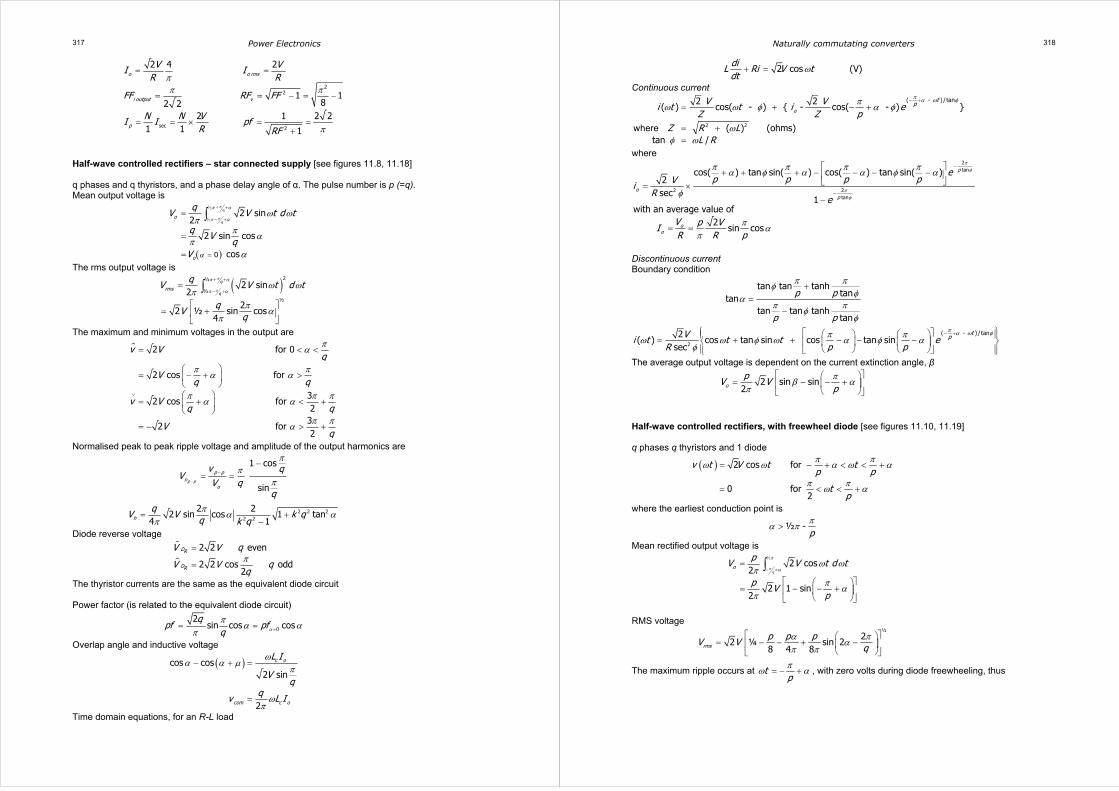
Power Electronics 317
.
.
.
22
sec 2
2 4 2
1 182 2
2 1 2 21 1 1
o o rms
i output v
p
V VI IR R
FF RF FF
N N VI I pfR RF
ππ π
π
= =
= = − = −
= = × = =+
Half-wave controlled rectifiers – star connected supply [see figures 11.8, 11.18] q phases and q thyristors, and a phase delay angle of α. The pulse number is p (=q). Mean output voltage is
( )
q
q
½ +
½
0
2 sin2
2 sin cos
cos
o
o
qV V t d t
q Vq
V
π
π
π α
π α
α
ω ωπ
π απα
+
− +
=
=
=
=
∫
The rms output voltage is
( )2½
½
½
2 sin2
22 ½ sin cos
4
q
qrms
qV V t d t
qV
q
π
π
π α
π αω ω
ππ α
π
+ +
− +=
= +
∫
The maximum and minimum voltages in the output are
.
.
.
.
2 for 0
2 cos for
32 cos for
23
2 for 2
v Vq
Vq q
v Vq q
Vq
πα
π πα α
π π πα α
π πα
∨
= < <
= − + >
= + < +
= − > +
Normalised peak to peak ripple voltage and amplitude of the output harmonics are
1 cos
sinp p
p pn
o
v qV
V qq
ππ
π−
−
−= =
.
2 2 22 2
2 22 sin cos 1 tan
4 1h
qV V k qq k qπ α α
π= +
−
Diode reverse voltage
2 2 even
2 2 cos odd2
DR
DR
V V q
V V qqπ
=
=
The thyristor currents are the same as the equivalent diode circuit Power factor (is related to the equivalent diode circuit)
0
2sin cos cos
qpf pf
q α
π α απ == =
Overlap angle and inductive voltage
( ).
cos cos2 sin
2
c o
com c o
L I
Vq
qv L I
ωα α µ
π
ωπ
− + =
=
Time domain equations, for an R-L load
Naturally commutating converters 318
2 cos (V)diL Ri V tdt
ω+ =
Continuous current
2 2
( - ) / tan2 2 ( ) cos( - ) - cos( - )
( ) (ohms)tan /
o
tpV Vi t t i e
Z Z pZ R L
L R
π α ω φπω ω φ α φ
ωφ ω
+−= + − +
= +=
where
where
.
2tan
2 2tan
cos( ) tan sin( ) cos( ) tan sin( )2 sec
1with an average value of
2sin cos
p
op
oo
ep p p pVi
Re
V p VIR R p
πφ
πφ
π π π πα φ α α φ α
φ
π απ
−
−
+ + + − − − −
= ×
−
= =
Discontinuous current Boundary condition
tan tan tanh
tantantan tan tanh
tan
p p
p p
π πφφα
π πφφ
+=
−
2
( - ) / tan2( ) cos tan sin cos tan sin
sec
tpVi t t t e
R p p
π α ω φπ πω ω φ ω α φ αφ
+− = + + − − −
The average output voltage is dependent on the current extinction angle, β
2 sin sin2o
pV V
pπβ α
π
= − − +
Half-wave controlled rectifiers, with freewheel diode [see figures 11.10, 11.19] q phases q thyristors and 1 diode
( ) 2 cos for
0 for 2
v t V t tp p
tp
π πω ω α ω α
π πω α
= − + < < +
= < < +
where the earliest conduction point is
½ -pπα π>
Mean rectified output voltage is
q
½2 cos
2
2 1 sin2
o
pV V t d t
p Vp
π
π
αω ω
ππ α
π
− +=
= − − +
∫
RMS voltage
½2
2 ¼ sin 28 4 8rms
p p pV Vq
α παπ π
= − − + −
The maximum ripple occurs at tpπω α= − + , with zero volts during diode freewheeling, thus

Power Electronics 319
2 cos 0
2 cos cos2
1 sin2 1 sin2
p p
p p
p pn
o
v Vp
Vv p p
VppV V
pp
π α
π πα απ
ππ ααπ
−
−
−
= − −
− − = = =
+ −− −
The freewheel diodes conduct for p periods of duration π/p+α, and the currents are
½
½ - ¼2
½ - ¼2
Df o
orms Df
p pI I
p pI I
απαπ
= +
= +
The thyristor conductor for 2π/p without a load freewheel diode and 2π/p-(π/p+α+½π) when the diode is present. The thyristor rms current is
½
½ - ¼2
ormsTh
I pI pq
απ
= +
Full-wave fully controlled thyristor converters–star connected supply [see figures 11.11, 11.12, 11.13, 11.20]
q phases 2q thyristors Pulse number, p
p=q if q is even p=2q if q is odd
Mean voltage
'sin cos coso o
pV V Vpπ α απ= =
The rms output voltage is
½
2½ sin cos
4o rms
pV V
pπ α
π
= +
The maximum and minimum voltages in the output are
for 0
cos for
3cos for
23
for 2
v Vp
Vp p
v Vp p
Vp
πα
π πα α
π π πα α
π πα
∨
= < <
= − + >
= + < +
= − > +
where
'
'
1
sin
22 sin
o
o
V Vp
pqV V
q
ππ
ππ
= ×
=
Thyristor maximum reverse and forward voltage
2 2 even
2 2 cos odd2
R
R
V V q
V V qqπ
=
=
RMS currents and power factor
0
2
sin cos cos
oTH TH rms o
II I I
q qqpf pf
q α
π α απ =
= =
= =
Naturally commutating converters 320
Overlap angle and inductive voltage
( ).
cos cos2 sin
c o
com c o
L I
Vq
qv L I
ωα α µ
π
ωπ
− − =
=
Half-controlled full bridges – star connected supply [see figures 11.7, 11.157, 11.22] q phases q thyristors and q diodes, each of which conduct for 2π/q Pulse number
p=q for all q, odd or even Mean voltage
( )'
'
2 sin 1 cos
1 cos2
2where 2 sin
o
o
o
qV Vq
V
qV Vq
π απα
ππ
= +
+=
=
Thyristor and diode reverse voltage
2 2 even
2 2 cos odd2
R
R
V V q
V V qqπ
=
=
Power factor
( )½ ½
.
.
2 2 1 cos 2sin
2
2 21 sin 1 cos
s o
s o
I I pf qq q q
I I pfq q
π α πα ππ
α π π πα α ππ π π α
+= = < −
= − = + > − −
Full-wave fully-controlled bridges – delta connected supply Pulse number in the rectified output is
p=q for q even p=2q for q odd
Thyristor maximum forward and reverse voltages
ππ
π
ππ
=
=
2 2 even
sin
2 2 cos2
oddsin
R
R
VV qq
q
VqV q
The power factor is the same as for the star case. Half-controlled full bridges – delta connected supply In terms of the semiconductors and rectified voltage star and mesh behave the same. Mean voltage, for all q is
( )'
'
2 sin 1 cos
1 cos2
2where 2 sin
o
o
o
qV Vq
V
qV Vq
π απα
ππ
= +
+=
=
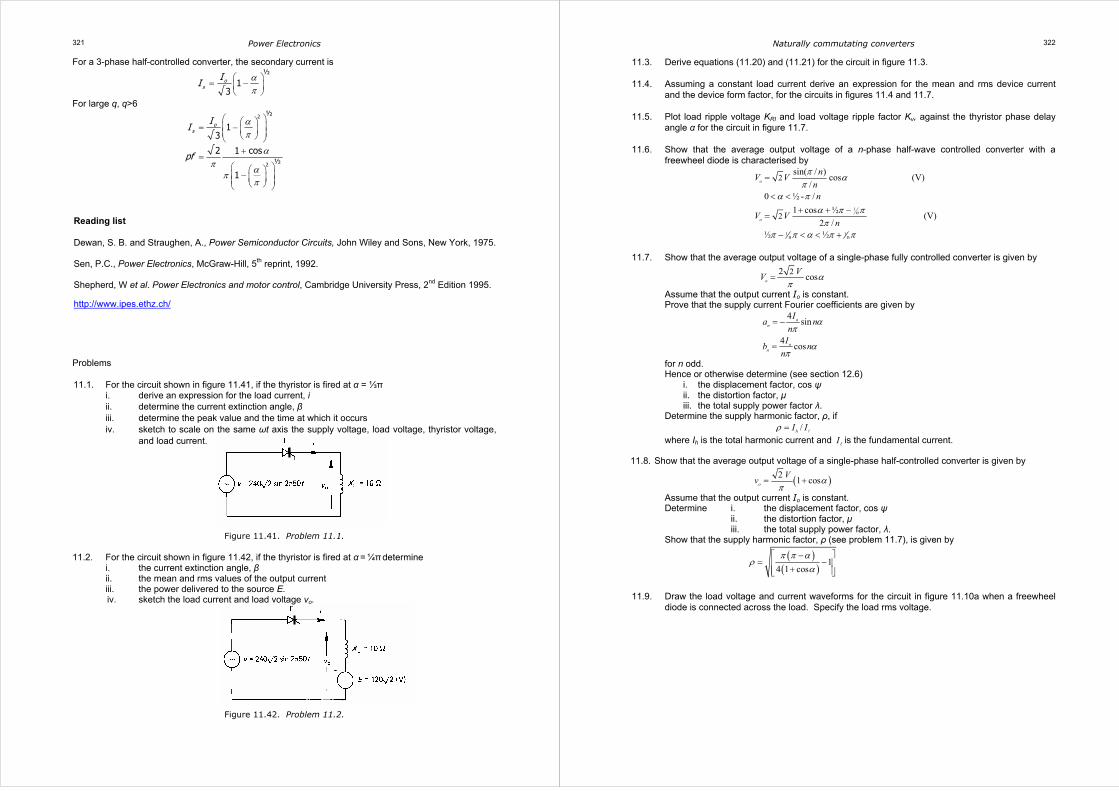
Power Electronics 321
For a 3-phase half-controlled converter, the secondary current is
.
½
13
os
II α
π = −
For large q, q>6
.
.
2
2
½
½
13
2 1 cos
1
os
II
pf
απ
απ απ
π
= − +
= −
Reading list Dewan, S. B. and Straughen, A., Power Semiconductor Circuits, John Wiley and Sons, New York, 1975. Sen, P.C., Power Electronics, McGraw-Hill, 5th reprint, 1992. Shepherd, W et al. Power Electronics and motor control, Cambridge University Press, 2nd Edition 1995. http://www.ipes.ethz.ch/ Problems 11.1. For the circuit shown in figure 11.41, if the thyristor is fired at α = ⅓π
i. derive an expression for the load current, i ii. determine the current extinction angle, β iii. determine the peak value and the time at which it occurs iv. sketch to scale on the same ωt axis the supply voltage, load voltage, thyristor voltage,
and load current.
Figure 11.41. Problem 11.1.
11.2. For the circuit shown in figure 11.42, if the thyristor is fired at α = ¼π determine
i. the current extinction angle, β ii. the mean and rms values of the output current iii. the power delivered to the source E. iv. sketch the load current and load voltage vo.
Figure 11.42. Problem 11.2.
Naturally commutating converters 322
11.3. Derive equations (11.20) and (11.21) for the circuit in figure 11.3. 11.4. Assuming a constant load current derive an expression for the mean and rms device current
and the device form factor, for the circuits in figures 11.4 and 11.7. 11.5. Plot load ripple voltage KRI and load voltage ripple factor Kv, against the thyristor phase delay
angle α for the circuit in figure 11.7. 11.6. Show that the average output voltage of a n-phase half-wave controlled converter with a
freewheel diode is characterised by
1
1 1n n
2
2
sin( / ) cos (V)/
0 ½ - /1 cos ½ (V)
2 /½ ½
o
o
n
nV V
nn
V Vn
π απ
α πα π ππ
π π α π π
=
< <+ + −
=
− < < +
11.7. Show that the average output voltage of a single-phase fully controlled converter is given by
22 coso
VV α
π=
Assume that the output current Io is constant. Prove that the supply current Fourier coefficients are given by
4 sin
4 cos
on
on
Ia n
nI
b nn
απ
απ
= −
=
for n odd. Hence or otherwise determine (see section 12.6)
i. the displacement factor, cos ψ ii. the distortion factor, µ iii. the total supply power factor λ.
Determine the supply harmonic factor, ρ, if /hI Iρ =
where Ih is the total harmonic current and I is the fundamental current. 11.8. Show that the average output voltage of a single-phase half-controlled converter is given by
( )2 1 coso
Vv α
π= +
Assume that the output current Io is constant. Determine i. the displacement factor, cos ψ
ii. the distortion factor, µ iii. the total supply power factor, λ.
Show that the supply harmonic factor, ρ (see problem 11.7), is given by
( )
( )1
4 1 cosπ π α
ρα
−= −
+
11.9. Draw the load voltage and current waveforms for the circuit in figure 11.10a when a freewheel
diode is connected across the load. Specify the load rms voltage.

Power Electronics 323
11.10. A centre tapped transformer, single-phase, full-wave converter (figure 11.11a) with a load freewheel diode is supplied from the 240 V ac, 50 Hz supply with source inductance of 0.25 mH. The continuous load current is 5 A. Find the overlap angles for
i. the transfer of current form a conducting thyristor to the load freewheel diode and ii. from the freewheel diode to a thyristor when the delay angle α is 30°.
1
1
2
2
cos 1 2.76 ;
cos cos 0.13
ot d
ot d
LI
V
LI
V
ωγ
ωγ α α
−−
−−
= − = ° = − − = °
11.11. The circuit in figure 11.8a, with v = √2 V sin(ωt + α), has a steady-state time response of
/2( ) sin( ) sin( ) Rt LVi t t e
Zω ω α φ α φ −= + − − −
where α is the trigger phase delay angle after voltage crossover and 1tan ( / )L Rφ ω−= Sketch the current waveform for α = ¼π and Z with
i. R >> ωL ii. R = ωL iii. R << ωL.
[(√2 V/R) sin(ωt + ¼π); (V/R) sin ωt; (V/ωL) (sin ωt - cos ωt + 1)] 11.12. A three-phase, fully-controlled converter is connected to the 415 V supply, which has a
reactance of 0.25 Ω/phase and resistance of 0.05 Ω/phase. The converter is operating in the inverter mode with α = 150º and a continuous 50 A load current. Assuming a thyristor voltage drop of 1.5 V at 50 A, determine the mean output voltage, overlap angle, and available recovery angle.
[-485.36 V -3 V -5 V -11.94 V = -505.3 V; 6.7°; 23.3°]
11.13. For the converter system in problem 11.12, what is the maximum dc current that can be accommodated at a phase delay of 165°, allowing for a recovery angle of 5°?
[35.53 A] 11.14. The single-phase half-wave controlled converter in figure 11.8 is operated from the 240 V, 50 Hz
supply and a 10 Ω resistive load. If the mean load voltage is 50 per cent of the maximum mean voltage, determine the (a) delay angle, α, (b) mean and rms load current, and (c) the input power factor.
11.15. The converter in figure 11.10a, with a freewheel diode, is operated from the 240 V, 50 Hz
supply. The load consists of, series connected, a 10 Ω resister, a 5 mH inductor and a 40 V battery. Derive the load voltage expression in the form of a Fourier series. Determine the rms value of the fundamental of the load current.
11.16. The converter in figure 11.7a is operated from the 240 V, 50 Hz supply with a load consisting of the series connection of a 10 Ω resistor, a 5 mH inductor, and a 40 V battery. Derive the load voltage expression in the form of a Fourier series. Determine the rms value of the fundamental of the load current.
11.17. The converter in figure 11.19 is operated from a Y-connected, 415 V, 50 Hz supply. If the load is
100 A continuous with a phase delay angle of π/6, calculate the (a) harmonic factor of the supply current, (b) displacement factor cos ψ, and (c) supply power factor, λ.
11.18. The converter in figure 11.19 is operated from the 415 V line-to-line voltage, 50 Hz supply, with
a series load of 10 Ω + 5 mH + 40 V battery. Derive the load voltage expression in terms of a Fourier series. Determine the rms value of the fundamental of the load current.
11.19. Repeat problem 11.18 for the three-phase, half-controlled converter in figure 11.17. 11.20. Repeat problem 11.18 for the three-phase, fully-controlled converter in figure 11.20. 11.21. The three-phase, half-controlled converter in figure 11.17 is operated from the 415 V, 50 Hz
supply, with a 100 A continuous load current. If the line inductance is 0.5 mH/phase, determine the overlap angle γ if (a) α = π/6 and (b) α = ⅔π.
Naturally commutating converters 324
11.22. Repeat example 11.1 using a 100Vac 60Hz supply. 11.23. A fully controlled half-wave rectifier has a resistive 30 Ω and a 240V ac 50Hz voltage source.
(a) If the delay angle α = 60º, determine: i. the average voltage across the load resistor ii. the power absorbed by the load resistor iii. the ac source power factor.
(b) If the average load current is 5A determine i. the average voltage across the load ii. the power absorbed by the load iii. the supply power factor.
11.24. A fully controlled half-wave rectifier has a 240V ac 50Hz source and a series R-L load of R =
20Ω and L = 50mH. If the delay angle is α = 60º, determine i. an expression for the load current ii. the average load current iii. the power absorbed by the load iv. the supply power factor
11.25. A single phase uncontrolled rectifier has a 24Ω resistive load a 240V ac 50Hz supply. Determine
the average, peak and rms current and peak reverse voltage across each rectifier diode for i. an isolating transformer with a 1:1 turns ratio ii. centre-tapped transformer with turns ratio 1:1:1.
11.26. A single phase bridge rectifier has an R-L of R = 20Ω and L = 50mH and a 240V ac 50Hz
source voltage. Determine: i. the average and rms currents of the diodes and load ii. rms and average 50Hz source currents iii. the power absorbed by the load iv. the supply power factor
11.27. An electromagnet is modelled by a series R-L circuit with R=10Ω and L=100mH, and supplied
from a 50Hz 240V ac voltage source. i. when supplied from a full-wave uncontrolled rectifier, the average current must be
20A to active the magnetic field. What series resistance must be added to increase the average current to 20A?
ii. when supplied from a full-wave fully-controlled converter, what delay angle will produce the necessary average current of 20A to activate the electro-magnet?
11.28. A single-phase, full-wave uncontrolled rectifier has a back emf Eb in its load. If the supply is
240Vac 50Hz and the series load is R = 20Ω, L = 50mH, and Eb = 120V dc, determine: i. the power absorbed by the dc source in the load ii. the power absorbed by the load resistor iii. the power delivered from the ac source iv. the ac source power factor v. the peak-to-peak load current variation if only the first ac term of the Fourier
series for the load current is considered. 11.29. Show that the power factor for a fully-controlled single-phase full-wave converter with a purely
resistive load is given by
α απ π
= − +sin2
12
pf
11.30. A fully controlled single-phase full-wave bridge converter has a 60 Ω resistive load and a 240V
ac 50Hz voltage source. If the firing delay angle is α = 60º, determine: i. the average load current ii. the rms load current iii. the rms source current iv. the ac source power factor

Power Electronics 325
11.31. A fully controlled single-phase full-wave bridge converter has an R-L load of 50 Ω and 50mH and is supplied from a 240V ac 50Hz voltage source. Determine the average load current if:
i. α = 15º ii. α = 75º
11.32. A three-phase uncontrolled rectifier is supplied from a 50Hz 415V ac line-to-line voltage source.
If the rectifier load is a 75 Ω resistor, determine i. the average load current ii. the rms load current iii. the rms source current iv. the supply power factor.
11.33. A three-phase uncontrolled rectifier is supplied from a 50Hz 415V ac line-to-line voltage source. If the rectifier load is a series R-L circuit where R = 10Ω and L = 100mH, determine:
i. the average and rms load currents ii. the average and rms diode currents iii. the rms source and power current iv. the supply power factor.
11.34. A three-phase, fully-controlled, converter is supplied from a 3.3kV ac 50Hz source. If the load is
a 110Ω resistor determine: i. the delay angle which results is an average load current of 20A ii. the amplitude of the first voltage harmonic (at 300Hz)
11.35. A three-phase, fully-controlled, converter is supplied from a 3.3kV ac 50Hz source. If the R-L
load is R = 100Ω and L=100mH, and the delay angle is α = 30º, determine: i. the average load current ii. the amplitude of the first current harmonic (at 300Hz) iii. the rms phase current from the ac voltage source.
Naturally commutating converters 326
Blank
Related Documents