11-1 Latches and Flip-Flops © 2010. Cengage Learning, Engineering. All Rights Reserved. 1-1 UNIT UNIT 11 11

11-0 Latches and Flip-Flops © 2010. Cengage Learning, Engineering. All Rights Reserved. 1-0 UNIT 11.
Dec 15, 2015
Welcome message from author
This document is posted to help you gain knowledge. Please leave a comment to let me know what you think about it! Share it to your friends and learn new things together.
Transcript
11-1
Latches and
Flip-Flops
© 2010. Cengage Learning, Engineering. All Rights Reserved.
1-1
UNIT UNIT 1111

11-2
Sequential logic circuits 1. A combinational circuit and a memory component 2. the output depends not only on the present input but also on the past sequence of inputs.

11-3
Figure 11.1Feedback feedback means that the output is connected back into the input gate in the Circuit so as to form a closed loop.
The output will continue to oscillate back and forth between 0 and 1.

11-4
Figure 11.2Stable state
11-5
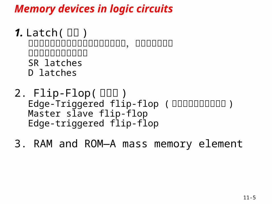
Memory devices in logic circuits
1. Latch( 閂鎖 )除非輸入信號送出來指示要切換狀態為止,該儲存元件可以無限期地維持原先的狀態SR latchesD latches
2. Flip-Flop( 正反器 )Edge-Triggered flip-flop ( 邊緣觸發型的記憶單元 )Master slave flip-flopEdge-triggered flip-flop
3. RAM and ROM—A mass memory element
11-6
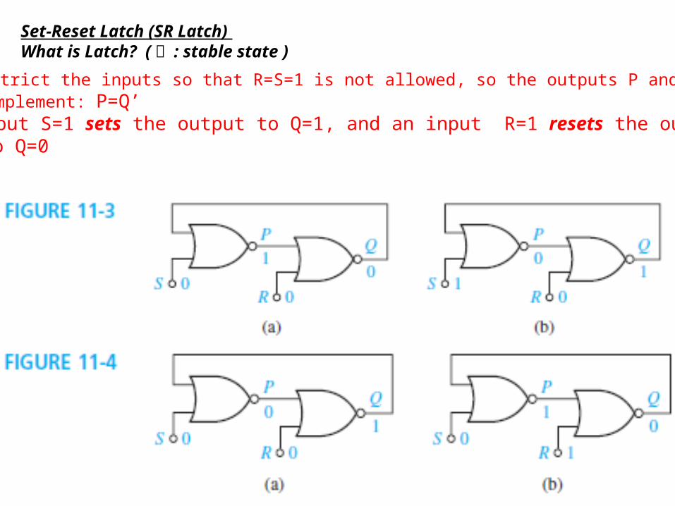
Figure 11.3Set-Reset Latch (SR Latch) What is Latch? ( 閂 : stable state )
1. We restrict the inputs so that R=S=1 is not allowed, so the outputs P and Q always complement: P=Q’ 2. An input S=1 sets the output to Q=1, and an input R=1 resets the output to Q=0

11-7
Figure 11.5 S-R LatchThe circuit and the symbol of a S-R Latch
Note that the symbol: Q directly above the S input

©2010 Cengage Learning Engineering. All Rights Reserved. 11-8
Figure 11.6 Improper S-R Latch Operation
Note that when S=R=1, the Latch will not operate properly
When S and R are both 1, P and Q are both 0. Therefore P is not equal to Q’.This violate a basic rule of latch operation that requires the latch output to complement.

©2010 Cengage Learning Engineering. All Rights Reserved. 11-9
• SR Latch :由一對 NOR 閘所構成之 SR 閂鎖器,兩個互補輸出
• 分為兩種狀態– S=1, R=0set state (Q 會變成 1)– S=0, R=1reset state (Q 會變成 0)– S=0, R=0 保持目前的值
The SR Latch

11-10
Figure 11.7 Timing Diagram for S-R Latch
The timing diagram for S-R latch
If the S or R input pulse is less than , the gate output will not change and the latch willNot change state.

11-11
Table 11.1 S-R Latch Next State and Output
Present state and next state in a Latch
Next state equation

11-12
Figure 11.8 Derivation of Q+ for an S-R Latch
From the K-map
When S=1 , next state is 1 R=0, Q=1, next state is 1
11-13
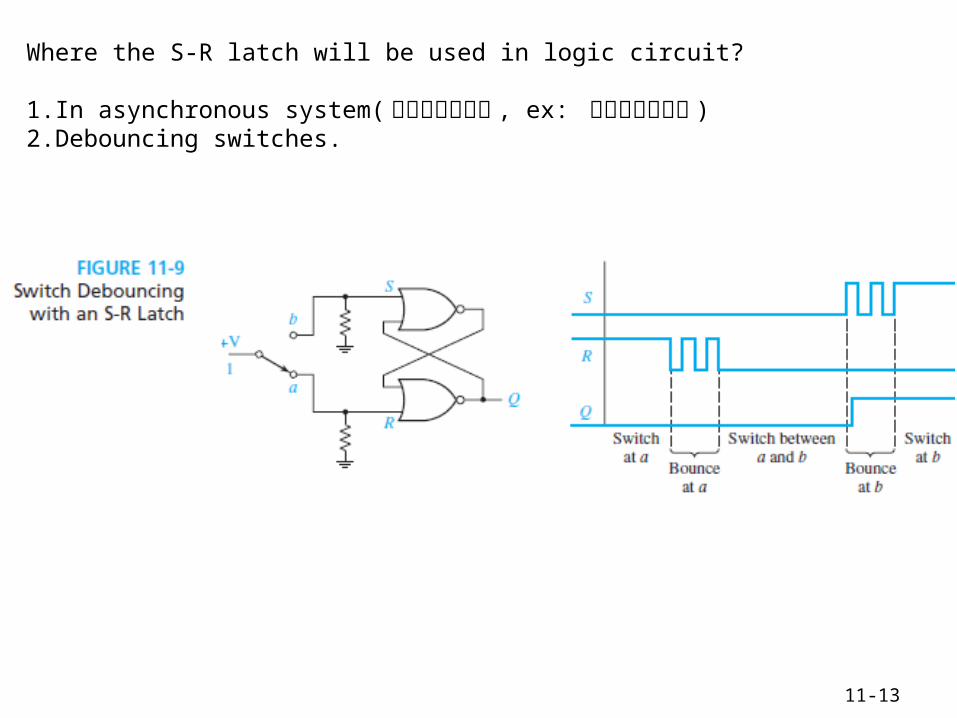
Figure 11.9 Switch Debouncing with an S-R Latch
Where the S-R latch will be used in logic circuit? 1.In asynchronous system( 非同步循序電路 , ex: 儲存二進位資訊 )2.Debouncing switches.
11-14
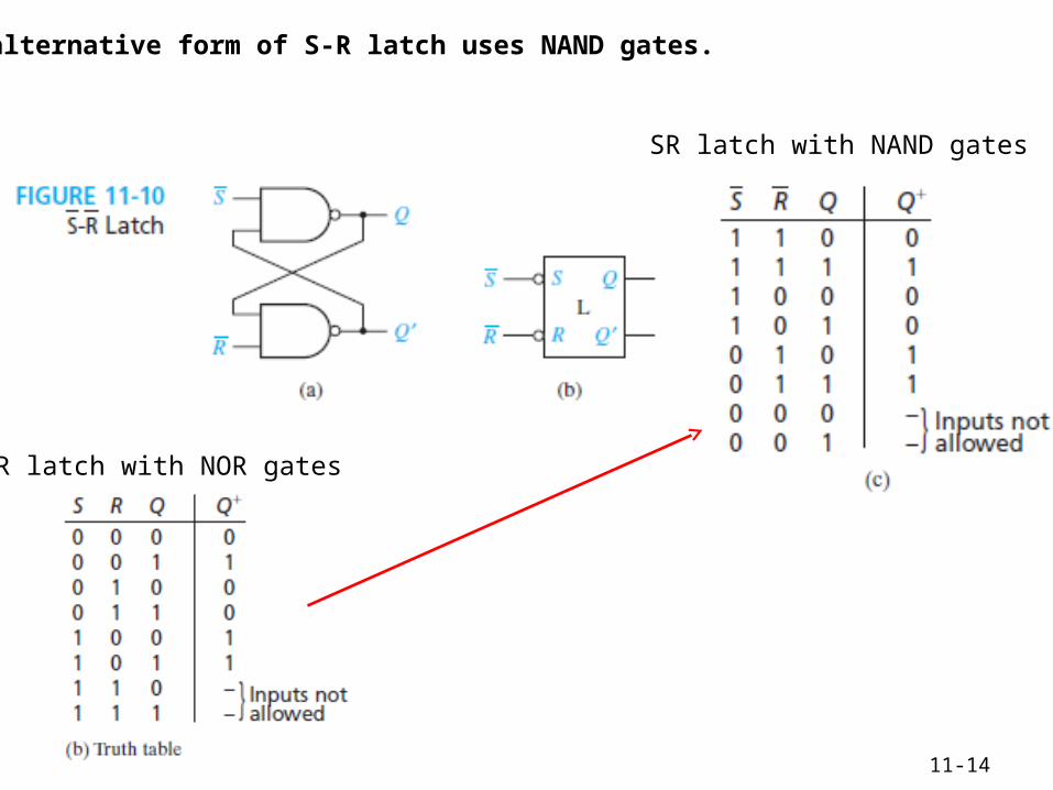
Figure 11.10 S-R LatchAn alternative form of S-R latch uses NAND gates.
SR latch with NOR gates
SR latch with NAND gates

11-15
Figure 11.11 Gated D LatchThe gated D Latch
1.This type of latch is referred to as a transparent latch: because when G=1, the Q output is same as D input.
Someone called this G inputas a control line.
Present state Input data Next state

11-16
Figure 11.13 D Flip-Flops
D Flip-Flop(FF)1.D-Latch 和 D Flip-Flop 皆為僅有一輸入端 (D) 的雙穩態記憶電路 (Q ,Q’) ,常用在資料儲存 與暫存器的使用。兩種元件都能將 D 之輸入端直接傳送到記憶體的輸出,但傳送的方式 不同 : a. FF: 由一個時序脈波 (Clock, Ck; a plus generator) 之邊緣輸入訊號 (edge- triggered signal) 來決定 D 輸出。 b. Latch: 當一個適當的邏輯準位加在致能端 (Enable input, G) ,則輸入之訊號變化 (D) 均會被傳送到輸出端。
©2010 Cengage Learning Engineering. All Rights Reserved. 11-17
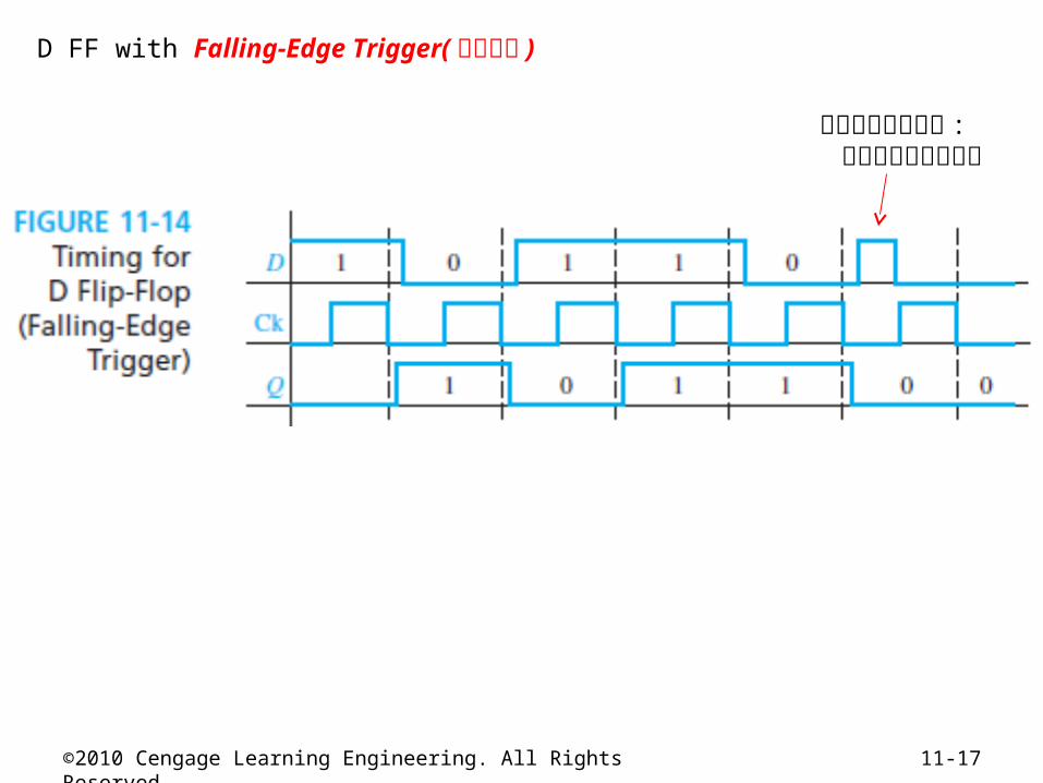
Figure 11.14 Timing for D Flip-Flop (Falling-Edge Trigger)
D FF with Falling-Edge Trigger( 負緣觸發 )
沒有被傳遞的訊號 : 不在觸發時發生變化

11-18
Figure 11.15 D Flip-Flop (Rising-Edge Trigger)
D FF with Rising-Edge Trigger( 正緣觸發 )
G2 觸發 (Q fow P)
G1 不觸發 (D stored, P unchanged)
G2 不 觸發 ( P stored, and Q unchanged)
G1 觸發 (P fow D)
G2 觸發 (Q fow P)
G1 不觸發 (D stored, P unchanged)
A rising-edge Triggered D-FF can be made by two gated D latches and one invertors

©2010 Cengage Learning Engineering. All Rights Reserved. 11-19
Figure 11.16 Setup and Hold Times for an Edge-Trimmed D
Flip-Flop
A flip-flop changes state only on the active edge of the clock. To function properly, the rule are:1.Before active edge, the D must stable for a setup time(tsu)2.After active edge, the D must stable for a hold time(th)3.The propagation delay(tp) from the time the clock changed.

11-20
Figure 11.17 Determination of Minimum Clock Period
To determine the minimum clock period1.Suppose the invertor have 2ns delay, and FF have 5ns delay. 2.Suppose the setup time is 3ns.
Ck period 7ns
Ck period 15ns Ck period 10ns

11-21
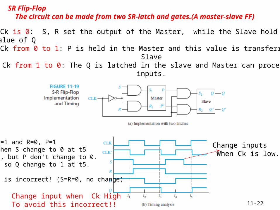
Figure 11.18 S-R Flip-FlopSR Flip-Flop
1. Similar to an S-R Latch in that S=1 set Q output to 1; and R=1 resets the output to 0. The difference is that FF has a clock(Ck) input, the Q can change only after an active clock edge.2. The truth table and next state equation(characteristic equation) is same as Latch.
11-22
Figure 11.19 S-R Flip-Flop Implementation and Timing
SR Flip-Flop The circuit can be made from two SR-latch and gates.(A master-slave FF)
1. When Ck is 0: S, R set the output of the Master, while the Slave hold the previous value of Q2. When Ck from 0 to 1: P is held in the Master and this value is transferred to the Slave3. When Ck from 1 to 0: The Q is latched in the slave and Master can process new inputs.
Change inputs When Ck is low.
1. S=1 and R=0, P=12. When S change to 0 at t5 , but P don’t change to 0. so Q change to 1 at t5.
This is incorrect! (S=R=0, no change)
Change input when Ck High To avoid this incorrect!!

11-23
Figure 11.20 J-K Flip-Flop (Q Changes on the Rising Edge)
J-K Flip-Flop
1. 與 SR FF 相似,主要差別在於, SR FF 在兩個輸入端皆為 1 時,會發生不確定之輸出, 而 J-K FF 的輸出狀態會反相,可以消除 SR FF 的不確定狀態。2. 三個 inputs: Ck, J , K
S R
1
0
0
1
1
1

11-24
Figure 11.21 Master Slave J-K Flip-Flop (Q Changes on Rising
Edge)
J-K Flip-Flop circuitJK FF 一般以兩 SR Latch 和 gate 連結,以 master-slave 架構來實現1.與 SR FF 電路相似,差別僅在於把 input S,R 換成 J, K. 且 output 需 feedback 到 input gate.2. S= JQ’Ck’ and R=KQCk’
11-25
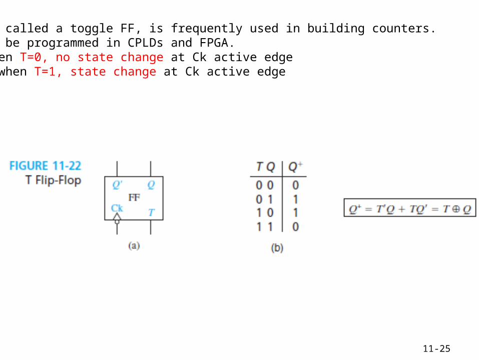
Figure 11.22 T Flip-FlopT Flip-Flop: 1. Also called a toggle FF, is frequently used in building counters. 2. Can be programmed in CPLDs and FPGA. 3. when T=0, no state change at Ck active edge when T=1, state change at Ck active edge
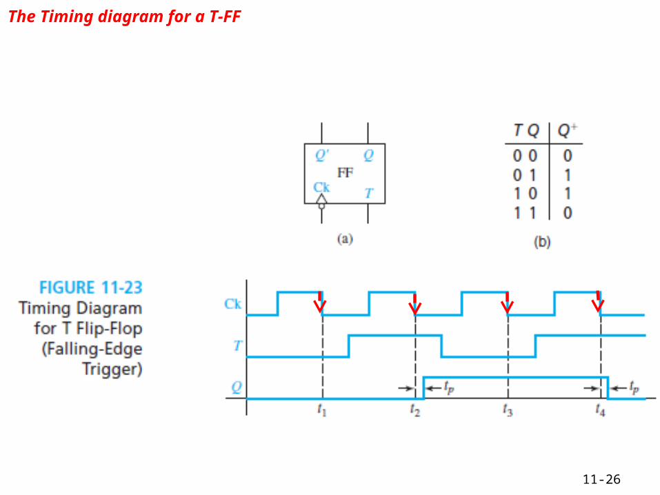
11-26
Figure 11.23 Timing Diagram for T Flip-Flop (Falling Edge
Trigger)
The Timing diagram for a T-FF

11-27
Figure 11.24 Implementation of T Flip-Flops
Implement a T-FF circuit
Connect the J,K inputs.
J-K FF D FF

11-28
Figure 11.25 D Flip-Flop with Clear and Preset
Filp-Flop with Additional Inputs
1.Can be used to set the FF to an initial state independent of the clock.2.ClrN: Clear Notation3.PreN: Present Notation
Note the inverter, so ClrN and PreN is active-low( 低準位觸發反應 )
1. 當 PreN, ClrN 皆為 0 ,不允許2. 當 PreN 為 0, 不管其他如何 , output 強制設置為 13. 當 ClrN 為 0, 不管其他如何 , output 強制歸為 0.4. 當 PreN 和 ClrN 皆為 1, 依循 D-FF 原本 之操作 : 在 Ck 產生邊緣觸發時,傳送 D 至 output.

11-29
Figure 11.26 Timing Diagram for D Flip-Flop with Asynchronous
Clear and Preset
The timming Diagram for a D-FF with ClrN and PreN
由於 ClrN =0強制 Q 為 0( 雖然在 Ck rising-edge)
過程中 ClrN 回到 1兩者皆為 1 ,因此回到原本操作在下一個 Ck rising edge 觸發點 , 看 D輸出
D 此時變 0
由於 PreN =0強制 Q 為 1
過程中 PreN 回到 1兩者皆為 1 ,因此回到原本操作在下一個 Ck rising edge 觸發點 , 看 D輸出
11-30
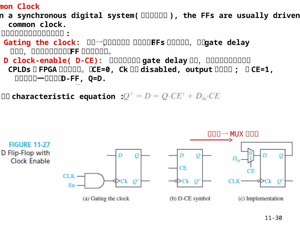
Figure 11.27 D Flip-Flop with Clock Enable
Common Clock1.In a synchronous digital system( 同步數位系統 ), the FFs are usually driven by a common clock. 2. 以下兩種方式可以實現這樣電路 : a. Gating the clock: 存在一個潛在問題,當並接多個 FFs 的同步電路,因為 gate delay 的問題,導致實際傳達到每個 FF 的時間不同步。 b. D clock-enable( D-CE): 可以解決上述的 gate delay 問題,且這樣的電路常使用在 CPLDs 和 FPGA 電路設計中。當 CE=0, Ck 變成 disabled, output 維持不變 ; 當 CE=1, 元件操作為一個典型的 D-FF, Q=D.
所以 characteristic equation :
可以由一 MUX 來實現

11-31
Summary
1.SR latch and SR-FF2.Gated D latch and D-FF3.D-CE FF4.JK-FF5.T-FF
Note that JK-FF and D-FF can convert to a T-FF
The next-state (characteristic)equations:
11-32
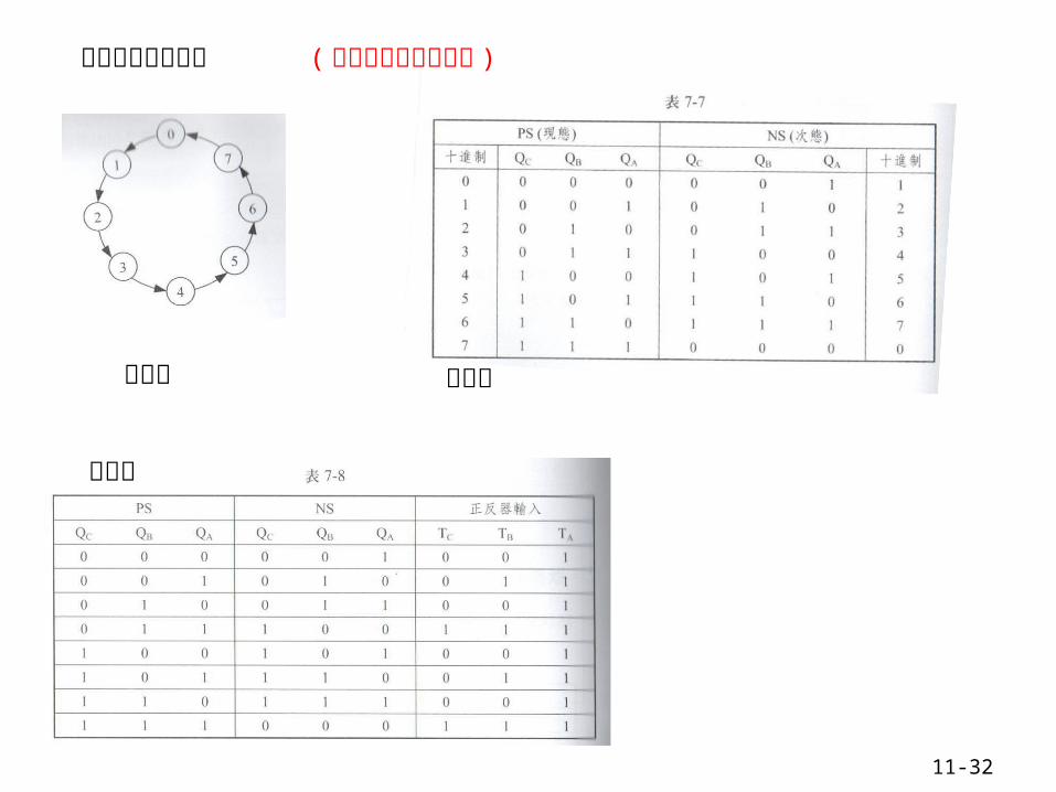
循序電路的設計法
狀態圖
( 以二進制計數器為例 )
狀態表
輸入表

11-33
K-map
邏輯電路

©2010 Cengage Learning Engineering. All Rights Reserved. 11-34
Ch11 HW11.811.9 11.2111.24
Related Documents