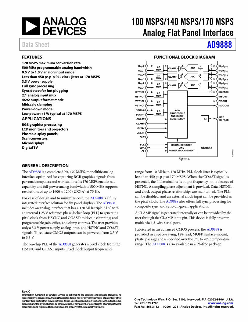
100 MSPS/140 MSPS/170 MSPS Analog Flat Panel Interface Data Sheet AD9888 Rev. C Information furnished by Analog Devices is believed to be accurate and reliable. However, no responsibility is assumed by Analog Devices for its use, nor for any infringements of patents or other rights of third parties that may result from its use. Specifications subject to change without notice. No license is granted by implication or otherwise under any patent or patent rights of Analog Devices. Trademarks and registered trademarks are the property of their respective owners. One Technology Way, P.O. Box 9106, Norwood, MA 02062-9106, U.S.A. Tel: 781.329.4700 www.analog.com Fax: 781.461.3113 ©2001–2011 Analog Devices, Inc. All rights reserved. FEATURES 170 MSPS maximum conversion rate 500 MHz programmable analog bandwidth 0.5 V to 1.0 V analog input range Less than 450 ps p-p PLL clock jitter at 170 MSPS 3.3 V power supply Full sync processing Sync detect for hot plugging 2:1 analog input mux 4:2:2 output format mode Midscale clamping Power-down mode Low power: <1 W typical at 170 MSPS APPLICATIONS RGB graphics processing LCD monitors and projectors Plasma display panels Scan converters Microdisplays Digital TV FUNCTIONAL BLOCK DIAGRAM HSYNC0 VSYNC0 VSYNC1 SOGIN0 SOGIN1 COAST HSYNC1 SERIAL REGISTER AND POWER MANAGEMENT DATACK HSOUT VSOUT SOGOUT AD9888 SYNC PROCESSING AND CLOCK GENERATION CLAMP D R A [7:0] D R B [7:0] D G A [7:0] D G B [7:0] D B A [7:0] D B B [7:0] ADC CLAMP R AIN 1 R AIN 0 8 8 8 ADC CLAMP 8 8 8 ADC CLAMP 2:1 MUX SCL SDA A0 8 8 8 2 G AIN 1 G AIN 0 B AIN 1 B AIN 0 2:1 MUX 2:1 MUX REF BYPASS 2:1 MUX 2:1 MUX 2:1 MUX CKINV CKEXT FILT REF 02442-001 Figure 1. GENERAL DESCRIPTION The AD9888 is a complete 8-bit, 170 MSPS, monolithic analog interface optimized for capturing RGB graphics signals from personal computers and workstations. Its 170 MSPS encode rate capability and full-power analog bandwidth of 500 MHz supports resolutions of up to 1600 × 1200 (UXGA) at 75 Hz. For ease of design and to minimize cost, the AD9888 is a fully integrated interface solution for flat panel displays. The AD9888 includes an analog interface that has a 170 MHz triple ADC with an internal 1.25 V reference phase-locked loop (PLL) to generate a pixel clock from HSYNC and COAST; midscale clamping; and programmable gain, offset, and clamp controls. The user provides only a 3.3 V power supply, analog input, and HSYNC and COAST signals. Three-state CMOS outputs can be powered from 2.5 V to 3.3 V. The on-chip PLL of the AD9888 generates a pixel clock from the HSYNC and COAST inputs. Pixel clock output frequencies range from 10 MHz to 170 MHz. PLL clock jitter is typically less than 450 ps p-p at 170 MSPS. When the COAST signal is presented, the PLL maintains its output frequency in the absence of HSYNC. A sampling phase adjustment is provided. Data, HSYNC, and clock output phase relationships are maintained. The PLL can be disabled, and an external clock input can be provided as the pixel clock. The AD9888 also offers full sync processing for composite sync and sync-on-green applications. A CLAMP signal is generated internally or can be provided by the user through the CLAMP input pin. This device is fully program- mable via a 2-wire serial port. Fabricated in an advanced CMOS process, the AD9888 is provided in a space-saving, 128-lead, MQFP, surface-mount, plastic package and is specified over the 0°C to 70°C temperature range. The AD9888 is also available in a Pb-free package.

Welcome message from author
This document is posted to help you gain knowledge. Please leave a comment to let me know what you think about it! Share it to your friends and learn new things together.
Transcript
100 MSPS/140 MSPS/170 MSPS Analog Flat Panel Interface
Data Sheet AD9888
Rev. C Information furnished by Analog Devices is believed to be accurate and reliable. However, no responsibility is assumed by Analog Devices for its use, nor for any infringements of patents or other rights of third parties that may result from its use. Specifications subject to change without notice. No license is granted by implication or otherwise under any patent or patent rights of Analog Devices. Trademarks and registered trademarks are the property of their respective owners.
One Technology Way, P.O. Box 9106, Norwood, MA 02062-9106, U.S.A.Tel: 781.329.4700 www.analog.com Fax: 781.461.3113 ©2001–2011 Analog Devices, Inc. All rights reserved.
FEATURES 170 MSPS maximum conversion rate 500 MHz programmable analog bandwidth 0.5 V to 1.0 V analog input range Less than 450 ps p-p PLL clock jitter at 170 MSPS 3.3 V power supply Full sync processing Sync detect for hot plugging 2:1 analog input mux 4:2:2 output format mode Midscale clamping Power-down mode Low power: <1 W typical at 170 MSPS
APPLICATIONS RGB graphics processing LCD monitors and projectors Plasma display panels Scan converters Microdisplays Digital TV
FUNCTIONAL BLOCK DIAGRAM
HSYNC0
VSYNC0
VSYNC1
SOGIN0
SOGIN1
COAST
HSYNC1
SERIAL REGISTERAND
POWER MANAGEMENT
DATACK
HSOUT
VSOUT
SOGOUT
AD9888
SYNCPROCESSINGAND CLOCK
GENERATION
CLAMP
DRA[7:0]
DRB[7:0]
DGA[7:0]
DGB[7:0]
DBA[7:0]
DBB[7:0]
ADCCLAMPRAIN1
RAIN0 8
88
ADCCLAMP8
88
ADCCLAMP
2:1MUX
SCLSDA
A0
8
88
2
GAIN1
GAIN0
BAIN1
BAIN0
2:1MUX
2:1MUX
REFBYPASS
2:1MUX
2:1MUX
2:1MUX
CKINV
CKEXT
FILT
REF
0244
2-00
1
Figure 1.
GENERAL DESCRIPTION The AD9888 is a complete 8-bit, 170 MSPS, monolithic analog interface optimized for capturing RGB graphics signals from personal computers and workstations. Its 170 MSPS encode rate capability and full-power analog bandwidth of 500 MHz supports resolutions of up to 1600 × 1200 (UXGA) at 75 Hz.
For ease of design and to minimize cost, the AD9888 is a fully integrated interface solution for flat panel displays. The AD9888 includes an analog interface that has a 170 MHz triple ADC with an internal 1.25 V reference phase-locked loop (PLL) to generate a pixel clock from HSYNC and COAST; midscale clamping; and programmable gain, offset, and clamp controls. The user provides only a 3.3 V power supply, analog input, and HSYNC and COAST signals. Three-state CMOS outputs can be powered from 2.5 V to 3.3 V.
The on-chip PLL of the AD9888 generates a pixel clock from the HSYNC and COAST inputs. Pixel clock output frequencies
range from 10 MHz to 170 MHz. PLL clock jitter is typically less than 450 ps p-p at 170 MSPS. When the COAST signal is presented, the PLL maintains its output frequency in the absence of HSYNC. A sampling phase adjustment is provided. Data, HSYNC, and clock output phase relationships are maintained. The PLL can be disabled, and an external clock input can be provided as the pixel clock. The AD9888 also offers full sync processing for composite sync and sync-on-green applications.
A CLAMP signal is generated internally or can be provided by the user through the CLAMP input pin. This device is fully program-mable via a 2-wire serial port.
Fabricated in an advanced CMOS process, the AD9888 is provided in a space-saving, 128-lead, MQFP, surface-mount, plastic package and is specified over the 0°C to 70°C temperature range. The AD9888 is also available in a Pb-free package.
AD9888 Data Sheet
Rev. C | Page 2 of 36
TABLE OF CONTENTS Features .............................................................................................. 1
Applications....................................................................................... 1
Functional Block Diagram .............................................................. 1
General Description ......................................................................... 1
Revision History ............................................................................... 3
Specifications..................................................................................... 4
Absolute Maximum Ratings............................................................ 6
Explanation of Test Levels ........................................................... 6
ESD Caution.................................................................................. 6
Pin Configuration and Function Descriptions............................. 7
Design Guide................................................................................... 12
General Description................................................................... 12
Input Signal Handling................................................................ 12
Sync Processing Overview ........................................................ 12
HSYNC and VSYNC Inputs...................................................... 12
Serial Control Port ..................................................................... 12
Output Signal Handling............................................................. 12
Clamping ..................................................................................... 12
Gain and Offset Control ............................................................ 13
Sync-on-Green Input ................................................................. 14
Clock Generation ....................................................................... 14
Alternate Pixel Sampling Mode................................................ 16
Timing.......................................................................................... 17
2-Wire Serial Register Map ........................................................... 21
2-Wire Serial Control Register Details ........................................ 24
Chip Identification ..................................................................... 24
PLL Divider Control .................................................................. 24
Clock Generator Control .......................................................... 24
Clamp Timing............................................................................. 24
HSYNC Pulse Width.................................................................. 25
Input Gain ................................................................................... 25
Input Offset ................................................................................. 25
Sync Control ............................................................................... 25
Input Control .............................................................................. 26
Mode Control 1 .......................................................................... 29
2-Wire Serial Control Port ............................................................ 31
Data Transfer via Serial Interface............................................. 31
Sync Processing .......................................................................... 32
Sync Slicer.................................................................................... 33
Sync Separator ............................................................................ 33
PCB Layout Recommendations.................................................... 34
Analog Interface Inputs ............................................................. 34
Power Supply Bypassing ............................................................ 34
PLL ............................................................................................... 34
Outputs (Both Data and Clocks).............................................. 34
Digital Inputs .............................................................................. 35
Voltage Reference ....................................................................... 35
Outline Dimensions ....................................................................... 36
Ordering Guide .......................................................................... 36
Data Sheet AD9888
Rev. C | Page 3 of 36
REVISION HISTORY 12/11—Rev. B to Rev. C
Updated Format.................................................................. Universal Deleted AD9888AKSZ-205 Model .................................. Universal Changed Maximum Conversion Rate from
205 MSPS to 170 MSPS ............................................ Throughout Changes to Figure 1 and General Description ..............................1 Deleted AD9888KS-205 Columns, Changes to tDHO Parameter,
Table 1.............................................................................................4 Changes to Output Voltage, Low (VOL) Parameter, Table 1;
Moved Figure 2..............................................................................5 Changes to Table 2 and ESD Caution Section...............................6 Changes to Table 3 ............................................................................8 Changes to Table 4 ............................................................................9 Changes to YUV Clamping Section and to Gain and Offset
Control Section............................................................................13 Changes to Sync-on-Green Input Section and to Figure 8........14 Changes to Table 5 ..........................................................................15 Moved Figure 10, Figure 11, and Figure 12 .................................16 Changes to Captions of Figure 16 Through Figure 25 ...............17 Changes to Table 8 ..........................................................................21 Changes to Chip Identification Section .......................................24 Changes to Table 14 and Table 17 .................................................26 Changes to Address 0x10[7:3]—Sync-on-Green Slicer Threshold
Section and to Address 0x11[7:0]—Sync Separator Threshold Section ..........................................................................................27
Changes to Address 0x14[6]—Active HSYNC (AHS) Section, Added Table 29, Changes to Address 0x14[3]—Active VSYNC (AVS) Section, Added Table 33, Changes to Table 34.........................................................................................28
Changes to Address 0x15[6]—Output Mode Section and to Address 0x15[5]—A/B Invert Control (OUTPHASE) Section ..........................................................................................29
Moved Figure 26..............................................................................31
Moved Figure 27..............................................................................32 Changes to Outputs (Both Data and Clocks) Section................34 Changes to Voltage Reference Section .........................................35 Updated Outline Dimensions........................................................36 Changes to Ordering Guide...........................................................36
3/03—Rev. A to Rev. B
Changes to Specifications ...............................................................2 Changes to Pin Configuration.........................................................4 Changes to Table II .........................................................................11 Changes to Table IV........................................................................11 Changes to Figure 20 ......................................................................16 Changes to Figure 22 ......................................................................17 Changes to Table V .........................................................................17 Changes to Table VI........................................................................20 Changes to Table XIII .....................................................................22 Changes to Clamp Input Signal Source Section..........................22 Changes to Table XXX....................................................................24 Added text to Outputs (Both Data and Clocks) Section ...........29 Updated Outline Dimensions........................................................30
1/02—Rev. 0 to Rev. A.
Change to Title–Part Name .............................................................1 Change to Pin Function Detail, CKINV Section..........................7 Change to Figure 13..........................................................................5 Change to Figure 14........................................................................15 Change to Figure 15........................................................................16 Change to Figure 16........................................................................16 Change to Figure 17........................................................................17 Change to Figure 18 .......................................................................17 Change to Figure 21........................................................................19 Change to Figure 22........................................................................19
7/01—Revision 0: Initial Version
AD9888 Data Sheet
Rev. C | Page 4 of 36
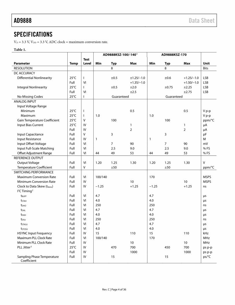
SPECIFICATIONS VD = 3.3 V, VDD = 3.3 V, ADC clock = maximum conversion rate.
Table 1. AD9888KSZ-100/-1401 AD9888KSZ-170
Parameter Temp Test Level Min Typ Max Min Typ Max Unit
RESOLUTION 8 8 Bits DC ACCURACY
Differential Nonlinearity 25°C I ±0.5 ±1.25/−1.0 ±0.6 +1.25/−1.0 LSB Full VI +1.35/−1.0 +1.50/−1.0 LSB Integral Nonlinearity 25°C I ±0.5 ±2.0 ±0.75 ±2.25 LSB Full VI ±2.5 ±2.75 LSB No Missing Codes 25°C I Guaranteed Guaranteed
ANALOG INPUT Input Voltage Range
Minimum 25°C I 0.5 0.5 V p-p Maximum 25°C I 1.0 1.0 V p-p
Gain Temperature Coefficient 25°C V 100 100 ppm/°C Input Bias Current 25°C IV 1 1 μA
Full IV 2 2 μA Input Capacitance Full V 3 3 pF Input Resistance Full IV 1 1 M Input Offset Voltage Full VI 7 90 7 90 mV Input Full-Scale Matching Full VI 2.5 9.0 2.5 9.0 % FS Offset Adjustment Range Full VI 44 49 53 44 49 53 % FS
REFERENCE OUTPUT Output Voltage Full VI 1.20 1.25 1.30 1.20 1.25 1.30 V Temperature Coefficient Full V ±50 ±50 ppm/°C
SWITCHING PERFORMANCE Maximum Conversion Rate Full VI 100/140 170 MSPS Minimum Conversion Rate Full IV 10 10 MSPS Clock to Data Skew (tskew) Full IV −1.25 +1.25 −1.25 +1.25 ns I2C Timing2
tBUFF Full VI 4.7 4.7 μs tSTAH Full VI 4.0 4.0 μs tDHO Full VI 250 250 ns tDAL Full VI 4.7 4.7 μs tDAH Full VI 4.0 4.0 μs tDSU Full VI 250 250 ns tSTASU Full VI 4.7 4.7 μs tSTOSU Full VI 4.0 4.0 μs
HSYNC Input Frequency Full IV 15 110 15 110 kHz Maximum PLL Clock Rate Full VI 100/140 170 MHz Minimum PLL Clock Rate Full IV 10 10 MHz PLL Jitter3 25°C IV 470 700 450 700 ps p-p Full IV 1000 1000 ps p-p Sampling Phase Temperature
Coefficient Full IV 15 15 ps/°C
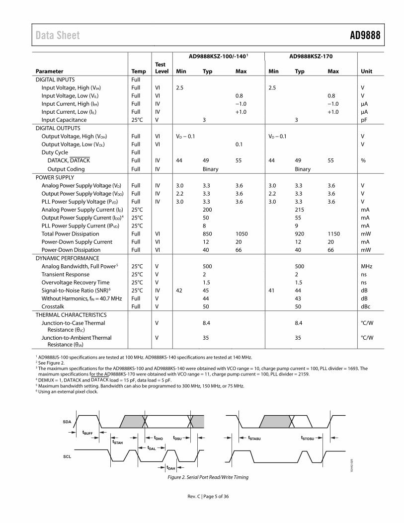
Data Sheet AD9888
Rev. C | Page 5 of 36
AD9888KSZ-100/-1401 AD9888KSZ-170
Parameter Temp Test Level Min Typ Max Min Typ Max Unit
DIGITAL INPUTS Full Input Voltage, High (VIH) Full VI 2.5 2.5 V Input Voltage, Low (VIL) Full VI 0.8 0.8 V Input Current, High (IIH) Full IV −1.0 −1.0 μA Input Current, Low (IIL) Full IV +1.0 +1.0 μA Input Capacitance 25°C V 3 3 pF
DIGITAL OUTPUTS Output Voltage, High (VOH) Full VI VD − 0.1 VD − 0.1 V Output Voltage, Low (VOL) Full VI 0.1 V Duty Cycle Full
DATACK, DATACK Full IV 44 49 55 44 49 55 %
Output Coding Full IV Binary Binary POWER SUPPLY
Analog Power Supply Voltage (VD) Full IV 3.0 3.3 3.6 3.0 3.3 3.6 V Output Power Supply Voltage (VDD) Full IV 2.2 3.3 3.6 2.2 3.3 3.6 V PLL Power Supply Voltage (PVD) Full IV 3.0 3.3 3.6 3.0 3.3 3.6 V Analog Power Supply Current (ID) 25°C 200 215 mA Output Power Supply Current (IDD)4 25°C 50 55 mA PLL Power Supply Current (IPVD) 25°C 8 9 mA Total Power Dissipation Full VI 850 1050 920 1150 mW Power-Down Supply Current Full VI 12 20 12 20 mA Power-Down Dissipation Full VI 40 66 40 66 mW
DYNAMIC PERFORMANCE Analog Bandwidth, Full Power5 25°C V 500 500 MHz Transient Response 25°C V 2 2 ns Overvoltage Recovery Time 25°C V 1.5 1.5 ns Signal-to-Noise Ratio (SNR)6 25°C IV 42 45 41 44 dB Without Harmonics, fIN = 40.7 MHz Full V 44 43 dB Crosstalk Full V 50 50 dBc
THERMAL CHARACTERISTICS Junction-to-Case Thermal
Resistance (θJC) V 8.4 8.4 °C/W
Junction-to-Ambient Thermal Resistance (θJA)
V 35 35 °C/W
1 AD9888JS-100 specifications are tested at 100 MHz. AD9888KS-140 specifications are tested at 140 MHz. 2 See Figure 2. 3 The maximum specifications for the AD9888KS-100 and AD9888KS-140 were obtained with VCO range = 10, charge pump current = 100, PLL divider = 1693. The
maximum specifications for the AD9888KS-170 were obtained with VCO range = 11, charge pump current = 100, PLL divider = 2159. 4 DEMUX = 1, DATACK and DATACK load = 15 pF, data load = 5 pF. 5 Maximum bandwidth setting. Bandwidth can also be programmed to 300 MHz, 150 MHz, or 75 MHz. 6 Using an external pixel clock.
tSTAHtDHO tDSU tSTASU tSTOSU
SCL
SDA
tBUFF
tDAL
tDAH
0244
2-02
5
Figure 2. Serial Port Read/Write Timing
AD9888 Data Sheet
Rev. C | Page 6 of 36
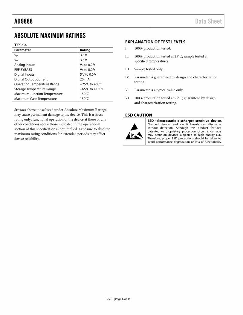
ABSOLUTE MAXIMUM RATINGS Table 2. Parameter Rating VD 3.6 V VDD 3.6 V Analog Inputs VD to 0.0 V REF BYBASS VD to 0.0 V Digital Inputs 5 V to 0.0 V Digital Output Current 20 mA Operating Temperature Range −25°C to +85°C Storage Temperature Range −65°C to +150°C Maximum Junction Temperature 150°C Maximum Case Temperature 150°C
Stresses above those listed under Absolute Maximum Ratings may cause permanent damage to the device. This is a stress rating only; functional operation of the device at these or any other conditions above those indicated in the operational section of this specification is not implied. Exposure to absolute maximum rating conditions for extended periods may affect device reliability.
EXPLANATION OF TEST LEVELS I. 100% production tested.
II. 100% production tested at 25°C; sample tested at specified temperatures.
III. Sample tested only.
IV. Parameter is guaranteed by design and characterization testing.
V. Parameter is a typical value only.
VI. 100% production tested at 25°C; guaranteed by design and characterization testing.
ESD CAUTION
Data Sheet AD9888
Rev. C | Page 7 of 36
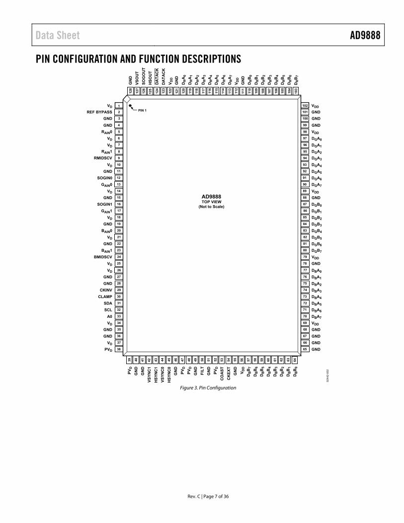
PIN CONFIGURATION AND FUNCTION DESCRIPTIONS
2REF BYPASS3GND4GND
7VD
6VD
5RAIN0
1VD
8RAIN19RMIDSCV
10VD
12SOGIN013GAIN014VD15GND16SOGIN117GAIN118VD19GND20BAIN021VD22GND23BAIN124BMIDSCV25VD26VD27GND28GND29CKINV30CLAMP31SDA32SCL33A034VD35GND36GND37VD38PVD
11GND
101 GND100 GND99 GND
96 DGA1
97 DGA0
98 VDD
102 VDD
95 DGA294 DGA393 DGA4
91 DGA690 DGA789 VDD88 GND87 DGB086 DGB185 DGB284 DGB383 DGB482 DGB581 DGB680 DGB779 VDD78 GND77 DBA076 DBA175 DBA274 DBA373 DBA472 DBA571 DBA670 DBA769 VDD68 GND67 GND66 GND65 GND
92 DGA5
39PV
D40
GN
D41
GN
D42
VSYN
C1
43H
SYN
C1
44VS
YNC
045
HSY
NC
046
GN
D47
PVD
48PV
D49
GN
D50
FILT
51G
ND
52PV
D53
CO
AST
54C
KEX
T55
GN
D56
V DD
57D
BB
758
DB
B6
59D
BB
560
DB
B4
61D
BB
362
DB
B2
63D
BB
164
DB
B0
128
GN
D12
7VS
OU
T12
6SO
GO
UT
125
HSO
UT
124
DA
TAC
K12
3D
ATA
CK
122
V DD
121
GN
D12
0D
RA
011
9D
RA
111
8D
RA
211
7D
RA
311
6D
RA
411
5D
RA
511
4D
RA
611
3D
RA
711
2V D
D11
1G
ND
110
DR
B0
109
DR
B1
108
DR
B2
107
DR
B3
106
DR
B4
105
DR
B5
104
DR
B6
103
DR
B7
PIN 1
AD9888TOP VIEW
(Not to Scale)
0244
2-00
2
Figure 3. Pin Configuration
AD9888 Data Sheet
Rev. C | Page 8 of 36
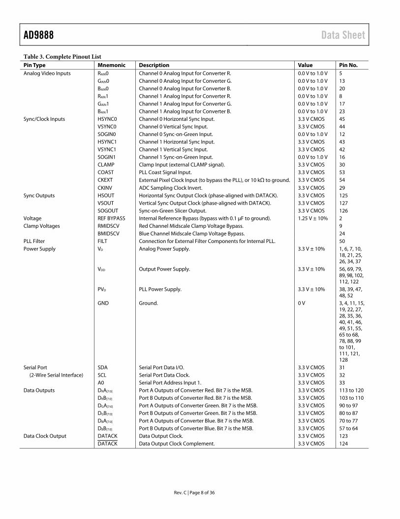
Table 3. Complete Pinout List Pin Type Mnemonic Description Value Pin No. Analog Video Inputs RAIN0 Channel 0 Analog Input for Converter R. 0.0 V to 1.0 V 5 GAIN0 Channel 0 Analog Input for Converter G. 0.0 V to 1.0 V 13 BAIN0 Channel 0 Analog Input for Converter B. 0.0 V to 1.0 V 20 RAIN1 Channel 1 Analog Input for Converter R. 0.0 V to 1.0 V 8 GAIN1 Channel 1 Analog Input for Converter G. 0.0 V to 1.0 V 17 BAIN1 Channel 1 Analog Input for Converter B. 0.0 V to 1.0 V 23 Sync/Clock Inputs HSYNC0 Channel 0 Horizontal Sync Input. 3.3 V CMOS 45 VSYNC0 Channel 0 Vertical Sync Input. 3.3 V CMOS 44 SOGIN0 Channel 0 Sync-on-Green Input. 0.0 V to 1.0 V 12 HSYNC1 Channel 1 Horizontal Sync Input. 3.3 V CMOS 43 VSYNC1 Channel 1 Vertical Sync Input. 3.3 V CMOS 42 SOGIN1 Channel 1 Sync-on-Green Input. 0.0 V to 1.0 V 16 CLAMP Clamp Input (external CLAMP signal). 3.3 V CMOS 30 COAST PLL Coast Signal Input. 3.3 V CMOS 53 CKEXT External Pixel Clock Input (to bypass the PLL), or 10 kΩ to ground. 3.3 V CMOS 54
CKINV ADC Sampling Clock Invert. 3.3 V CMOS 29 Sync Outputs HSOUT Horizontal Sync Output Clock (phase-aligned with DATACK). 3.3 V CMOS 125 VSOUT Vertical Sync Output Clock (phase-aligned with DATACK). 3.3 V CMOS 127 SOGOUT Sync-on-Green Slicer Output. 3.3 V CMOS 126 Voltage REF BYPASS Internal Reference Bypass (bypass with 0.1 μF to ground). 1.25 V ± 10% 2 Clamp Voltages RMIDSCV Red Channel Midscale Clamp Voltage Bypass. 9 BMIDSCV Blue Channel Midscale Clamp Voltage Bypass. 24 PLL Filter FILT Connection for External Filter Components for Internal PLL. 50 Power Supply VD Analog Power Supply. 3.3 V ± 10% 1, 6, 7, 10,
18, 21, 25, 26, 34, 37
VDD Output Power Supply. 3.3 V ± 10% 56, 69, 79, 89, 98, 102, 112, 122
PVD PLL Power Supply. 3.3 V ± 10% 38, 39, 47, 48, 52
GND Ground. 0 V 3, 4, 11, 15, 19, 22, 27, 28, 35, 36, 40, 41, 46, 49, 51, 55, 65 to 68, 78, 88, 99 to 101, 111, 121, 128
Serial Port SDA Serial Port Data I/O. 3.3 V CMOS 31 (2-Wire Serial Interface) SCL Serial Port Data Clock. 3.3 V CMOS 32
A0 Serial Port Address Input 1. 3.3 V CMOS 33 Data Outputs DRA[7:0] Port A Outputs of Converter Red. Bit 7 is the MSB. 3.3 V CMOS 113 to 120 DRB[7:0] Port B Outputs of Converter Red. Bit 7 is the MSB. 3.3 V CMOS 103 to 110 DGA[7:0] Port A Outputs of Converter Green. Bit 7 is the MSB. 3.3 V CMOS 90 to 97 DGB[7:0] Port B Outputs of Converter Green. Bit 7 is the MSB. 3.3 V CMOS 80 to 87 DBA[7:0] Port A Outputs of Converter Blue. Bit 7 is the MSB. 3.3 V CMOS 70 to 77 DBB[7:0] Port B Outputs of Converter Blue. Bit 7 is the MSB. 3.3 V CMOS 57 to 64 Data Clock Output DATACK Data Output Clock. 3.3 V CMOS 123 DATACK Data Output Clock Complement. 3.3 V CMOS 124
Data Sheet AD9888
Rev. C | Page 9 of 36
Table 4. Pin Function Descriptions Mnemonic Description Inputs
RAIN0 Channel 0 Analog Input for Red. GAIN0 Channel 0 Analog Input for Green. BAIN0 Channel 0 Analog Input for Blue. RAIN1 Channel 1 Analog Input for Red. GAIN1 Channel 1 Analog Input for Green. BAIN1 Channel 1 Analog Input for Blue. These high impedance inputs accept red, green, and blue channel graphics signals, respectively. The six channels are
identical and can be used for any color; colors are assigned for convenient reference. They accommodate input signals ranging from 0.5 V to 1.0 V full scale. Signals should be ac-coupled to these pins to support clamp operation.
HSYNC0 Channel 0 Horizontal Sync Input. HSYNC1 Channel 1 Horizontal Sync Input. These inputs receive a logic signal that establishes the horizontal timing reference and provides the frequency reference
for pixel clock generation. The logic sense of this pin is controlled by the HSYNC input polarity control (Register 0x0E, Bit 6). Only the leading edge of HSYNC is used by the PLL. The trailing edge is used for clamp timing only. When the HSYNC input polarity control = 0, the falling edge of HSYNC is used. When the HSYNC polarity control = 1, the rising edge is active. The input includes a Schmitt trigger for noise immunity, with a nominal input threshold of 1.5 V.
VSYNC0 Channel 0 Vertical Sync Input. VSYNC1 Channel 1 Vertical Sync Input. These are the inputs for vertical sync. SOGIN0 Channel 0 Sync-on-Green Input. SOGIN1 Channel 1 Sync-on-Green Input. These inputs are provided to assist in processing signals with embedded sync, typically on the green channel. These pins
are connected to a high speed comparator with an internally generated, variable threshold level, which is nominally set to 0.15 V above the negative peak of the input signal. When connected to an ac-coupled graphics signal with embedded sync, these pins produce a noninverting digital output on SOGOUT. This output is usually a composite sync signal, containing both vertical and horizontal sync information. When not used, these inputs should be left unconnected. For more details about this function and how it should be configured, see the Sync-on-Green Input section.
CLAMP External Clamp Input. This logic input can be used to define the time during which the input signal is clamped to the reference dc level (to
ground for RGB or to midscale for YUV). It should be used when the reference dc level is known to be present on the analog input channels, typically during a period following HSYNC, called the back porch, when a good black reference is provided. The CLAMP pin is enabled by setting the external clamp control (Register 0x0F, Bit 7) to 1 (default is 0). When disabled, this pin is ignored and the clamp timing is determined internally by counting a delay and duration from the trailing edge of the HSYNC input. The logic sense of this pin is controlled by the clamp polarity control (Register 0x0F, Bit 6). When not used, this pin should be grounded and the external clamp should be programmed to 0.
COAST Clock Generator Coast Input (optional). This input can be used to stop the pixel clock generator from synchronizing with HSYNC while continuing to produce a
clock at its current frequency and phase. This is useful when processing signals from sources that fail to produce horizontal sync pulses during the vertical interval or that include equalization pulses. The COAST signal is usually not required for PC generated signals. The logic sense of this pin is controlled by the coast polarity control (Register 0x0F, Bit 3). When this pin is not used, either ground the pin and program the coast polarity to 1 or tie the pin high (to VD through a 10 kΩ resistor) and program the coast polarity to 0. The coast polarity register bit defaults to 1 at power-up.
CKEXT External Clock Input (optional). This pin can be used to provide an external clock to the AD9888 in place of the clock internally generated from HSYNC. The
external clock is enabled by programming the external clock select bit (Register 0x15, Bit 0) to 1. When an external clock is used, all other internal functions operate normally. When not used, this pin should be tied through a 10 kΩ resistor to ground, and the external clock register should be programmed to 0. The clock phase adjustment still operates when an external clock source is used.
CKINV Sampling Clock Inversion (optional). This pin can be used to invert the pixel sampling clock, which has the effect of shifting the sampling phase 180°. This
supports the alternate pixel sampling mode, wherein higher frequency input signals (up to 410 MSPS) can be captured by first sampling the odd pixels, and then capturing the even pixels on the subsequent frame. This pin should be used only during blanking intervals (typically vertical blanking) because it might produce several samples of corrupted data during the phase shift. When not in use, this pin should be grounded.
AD9888 Data Sheet
Rev. C | Page 10 of 36
Mnemonic Description Outputs
DRA[7:0] Data Output, Red Channel, Port A. DRB[7:0] Data Output, Red Channel, Port B. DGA[7:0] Data Output, Green Channel, Port A. DGB[7:0] Data Output, Green Channel, Port B. DBA[7:0] Data Output, Blue Channel, Port A. DBB[7:0] Data Output, Blue Channel, Port B. Each channel has two ports. When the part is operated in single-channel mode (channel mode bit (Register 0x15, Bit 7) = 0),
all data is presented to Port A, and Port B is placed in a high impedance state. Programming the channel mode bit to 1 establishes dual-channel mode, where pixels are alternately presented to Port A and Port B of each channel. These appear simultaneously; two pixels are presented at the time of every second input pixel when the output mode bit (Register 0x15, Bit 6) is set to 1 (parallel mode). When the output mode bit is set to 0, pixel data appear alternately on the two ports, one new sample with each incoming pixel (interleaved mode). In dual-channel mode, the first pixel after HSYNC is routed to Port A. The second pixel goes to Port B, the third to Port A, and so on. This can be reversed by setting the A/B invert control bit (Register 0x15, Bit 5) to 1. The delay from the pixel sampling time to the output is fixed. When the sampling time is changed by adjusting the clock phase adjust register (Register 0x04, Bits[7:3]), the output timing is shifted as well. The DATACK, DATACK, and HSOUT outputs are also moved; therefore, the timing relationship among the signals is maintained.
DATACK, DATACK
Data Output Clock, Data Output Clock Complement.
These are differential data clock output signals to be used to strobe the output data and HSOUT into external logic. They are produced by the internal clock generator and are synchronous with the internal pixel sampling clock. When the AD9888 is operated in single-channel mode, the output frequency is equal to the pixel sampling frequency. When operated in dual-channel mode, the clock frequency is half the pixel frequency, as is the output data frequency. When the sampling time is changed by adjusting the clock phase adjust register (Register 0x04, Bits[7:3]), the output timing is shifted as well. The data, DATACK, DATACK, and HSOUT outputs are all moved; therefore, the timing relationship among the signals is maintained. Either or both signals can be used, depending on the timing mode and interface design used.
HSOUT Horizontal Sync Output. This is a reconstructed, phase-aligned version of the HSYNC input. Both the polarity and duration of this output can be
programmed via serial bus registers. By maintaining alignment with DATACK, DATACK, and data, data timing with respect to horizontal sync can always be determined.
VSOUT Verical Sync Output. SOGOUT Sync-on-Green (SOG) Slicer Output. This pin can be programmed to output either the sync-on-green slicer comparator or an unprocessed but delayed version
of the HSYNC input. See the sync processing block diagram (Figure 27) to view how this pin is connected. Note that other than slicing off SOG, the output from this pin receives no other additional processing on the AD9888. VSYNC separation is performed via the sync separator.
REF BYPASS Internal Reference Bypass. The absolute accuracy of this reference is ±4%, and the temperature coefficient is ±50 ppm, which is adequate for most
AD9888 applications. If higher accuracy is required, an external reference can be employed instead. RMIDSCV Red Channel Midscale Voltage Bypass. BMIDSCV Blue Channel Midscale Voltage Bypass. These bypasses for the internal midscale voltage references should each be connected to ground through 0.1 μF capacitors.
The exact voltage varies with the gain setting of the blue channel. FILT External Filter Connection. For proper operation, the internal PLL that generates the pixel clock requires an external filter.
Connect the filter shown in Figure 9 to this pin. For optimal performance, minimize noise and parasitics on this node. Power Supply
VD Main Power Supply. These pins supply power to the main elements of the circuit. This supply should be as quiet and filtered as possible.
VDD Digital Output Power Supply. A large number of output pins (up to 52) switching at high speed (up to 110 MHz) generates significant power supply
transients (noise). These supply pins are identified separately from the VD pins; therefore, special care must be taken to minimize output noise transferred into the sensitive analog circuitry. If the AD9888 is interfacing with lower voltage logic, VDD can be connected to a lower supply voltage (as low as 2.5 V) for compatibility.
PVD Clock Generator Power Supply. The most sensitive portion of the AD9888 is the clock generation circuitry. These pins provide power to the PLL generated pixel
clock and help the user design for optimal performance. The designer should provide noise-free power to these pins.
Data Sheet AD9888
Rev. C | Page 11 of 36
Mnemonic Description GND Ground. The ground return for all circuitry on the chip. It is recommended that the AD9888 be assembled on a single solid ground
plane, with careful attention paid to ground current paths. Serial Port
(2-Wire) For a full description of the 2-wire serial register and how it works, refer to the 2-Wire Serial Control Port section.
SDA Serial Port Data I/O. SCL Serial Port Data Clock. A0 Serial Port Address Input 1
AD9888 Data Sheet
Rev. C | Page 12 of 36
DESIGN GUIDE GENERAL DESCRIPTION The AD9888 is a fully integrated solution for capturing analog RGB signals and digitizing them for display on flat panel monitors or projectors. The circuit is ideal for providing a computer interface for HDTV monitors or for serving as the front end of high perfor-mance video scan converters.
Implemented in a high performance CMOS process, the interface can capture signals with pixel rates of up to 170 MHz, or of up to 340 MHz with an alternate pixel sampling mode.
The AD9888 includes all necessary input buffering, signal dc restoration (clamping), offset and gain (brightness and contrast) adjustment, pixel clock generation, sampling phase control, and output data formatting. All controls are programmable via a 2-wire serial interface. Full integration of these sensitive analog functions makes system design straightforward and less sensitive to the physical and electrical environment.
With a typical power dissipation of only 920 mW and an operating temperature range of 0°C to 70°C, the device requires no special environmental considerations.
INPUT SIGNAL HANDLING The AD9888 has six high impedance analog input pins for the red, green, and blue channels. They accommodate signals ranging from 0.5 V p-p to 1.0 V p-p.
Signals are typically brought onto the interface board via a digital visual interface integrated (DVI-I) connector, a 15-pin D connector, or BNC connectors. The AD9888 should be located as close as possible (or as close as is practical) to the input connector. Signals should be routed via matched impedance traces (normally 75 Ω) to the IC input pins.
At this point, the signal should be resistively terminated (to the signal ground return) and capacitively coupled to the AD9888 inputs through 47 nF capacitors. These capacitors form part of the dc restoration circuit.
If it were possible to have perfectly matched impedances, the best performance would be obtained with the widest possible signal bandwidth. The ultrawide bandwidth inputs of the AD9888 (500 MHz) would track the input signal continuously as it moved from one pixel level to the next, and then digitize the pixel during a long, flat pixel time. In real-world conditions, however, there are mismatches, reflections, and noise, which can result in excessive ringing and distortion of the input waveform. This makes it more difficult to establish a sampling phase that provides good image quality. The AD9888 can digitize graphics signals over a very wide range of frequencies (10 MHz to 170 MHz). Often, characteristics that are beneficial at one frequency can be detrimental at another. Analog bandwidth is one such characteristic. For UXGA resolutions (up to 170 MHz), a very high analog bandwidth is desirable because of the fast input signal slew rates. For VGA and lower
resolutions (down to 12.5 MHz), a very high bandwidth is not desirable because it allows excess noise to pass through. To accommodate these varying needs, the AD9888 includes a variable analog bandwidth control. Four settings are available (75 MHz, 150 MHz, 300 MHz, and 500 MHz), allowing the analog bandwidth to be matched with the resolution of the incoming graphics signal.
RGBINPUT
RAINGAINBAIN
47nF
75Ω
0244
2-00
3
Figure 4. Analog Input Interface Circuit
SYNC PROCESSING OVERVIEW The AD9888 circuitry enables it to accept composite sync inputs, such as sync-on-green or the trilevel sync inputs found in digital TV signals. A complete description of the sync processing functionality is found in the Sync Slicer and the Sync Separator sections.
HSYNC AND VSYNC INPUTS The interface can also accept a horizontal sync signal, which is used to generate the pixel clock and clamp timing. It is possible to operate the AD9888 without applying HSYNC (that is, by using an external clock, external clamp, and single port output mode), but a number of features of the chip will be unavailable; therefore, it is recommended that HSYNC be provided. This can be either a sync signal directly from the graphics source or a preprocessed TTL- or CMOS-level signal.
The HSYNC input includes a Schmitt-trigger buffer for immunity to noise and signals with long rise times. In typical PC-based graphics systems, the sync signals are simply TTL-level drivers feeding unshielded wires in the monitor cable. Therefore, no termination is required or desired.
SERIAL CONTROL PORT The serial control port is designed for 3.3 V logic. If there are 5 V drivers on the bus, these pins should be protected with 150 Ω series resistors placed between the pull-up resistors and the input pins.
OUTPUT SIGNAL HANDLING The digital outputs are designed and specified to operate from a 3.3 V power supply (VDD). They can also work with a VDD as low as 2.5 V for compatibility with other 2.5 V logic.
CLAMPING RGB Clamping
To digitize the incoming signal properly, the dc offset of the input must be adjusted to fit the range of the on-board ADCs.
Most graphics systems produce RGB signals with black at ground and white at approximately 0.75 V. However, if sync signals are embedded in the graphics, the sync tip is often at
Data Sheet AD9888
Rev. C | Page 13 of 36
ground, black is at 300 mV, and white is at approximately 1.0 V. Some common RGB line amplifier boxes use emitter-follower buffers to split signals and increase drive capability. This introduces a 700 mV dc offset to the signal, which must be removed for proper capture by the AD9888.
The key to clamping is to identify a time when the graphics system is known to be producing black. An offset is then introduced, which results in the ADCs producing a black output (Code 0x00) when the known black input is present. The offset then remains in place when other signal levels are processed, and the entire signal is shifted to eliminate offset errors.
In most graphics systems, black is transmitted between active video lines. In CRT displays, when the electron beam has completed writing a horizontal line on the right side of the screen, the beam is deflected quickly to the left side of the screen (called horizontal retrace), and a black signal is provided to prevent the beam from disturbing the image.
In systems with embedded sync, a blacker-than-black signal (HSYNC) is produced briefly to signal the CRT to begin a retrace. It is important to avoid clamping on the tip of HSYNC. Fortunately, there is almost always a period following HSYNC, called the back porch, when a good black reference is provided. This is the time when clamping should be performed.
The clamp timing can be established by simply exercising the CLAMP pin at the appropriate time with external clamp selected (clamp input signal source bit = 1). The polarity of this signal is set by the clamp polarity bit (Register 0x0F, Bit 6).
A simpler method of clamp timing employs the AD9888 internal clamp timing generator. The clamp placement register (Register 0x05) is programmed with the number of pixel times that should pass after the trailing edge of HSYNC before clamping begins. A second register (clamp duration, Register 0x06) sets the duration of the clamp. Both registers are 8-bit values, providing considerable flexibility in clamp generation. The clamp timing is referenced to the trailing edge of HSYNC, because, though HSYNC duration can vary widely, the back porch (black reference) always follows HSYNC. A good starting point for establishing clamping is to set the clamp placement to Value 0x08 (providing eight pixel periods for the graphics signal to stabilize after sync) and set the clamp duration to Value 0x14 (giving the clamp 20 pixel periods to reestablish the black reference).
Clamping is accomplished by placing an appropriate charge on the external input coupling capacitor. The value of this capacitor affects the performance of the clamp. If it is too small, there is a significant amplitude change during a horizontal line time (between clamping intervals). If the capacitor is too large, it takes an excessively long time for the clamp to recover from a large change in incoming signal offset. The recommended value (47 nF) results in recovering from a step error of 100 mV to within 1/2 LSB in 10 lines with a clamp duration of 20 pixel periods on a 60 Hz SXGA signal.
YUV Clamping
YUV graphics signals are slightly different from RGB signals in that the dc reference level (black level in RGB signals) can be at the midpoint of the video signal rather than at the bottom. For these signals, it might be necessary to clamp to the midscale of the ADC range (Value 0x80) rather than to the bottom of the ADC range (Value 0x00).
Clamping to midscale rather than to ground can be accomplished by setting the clamp select bits in Register 0x10. The red and blue channels each have their own selection bit so that they can be clamped to either midscale or ground independently. The clamp controls are located in Register 0x10, Bit 1 and Bit 2. The midscale reference voltage that each ADC clamps to is provided independently on the RMIDSCV and BMIDSCV pins. These two pins should be bypassed to ground using a 0.1 μF capacitor, even if midscale clamping is not required.
GAIN AND OFFSET CONTROL The AD9888 can accommodate input signals with inputs ranging from 0.5 V to 1.0 V full scale. The full-scale range is set in three 8-bit registers (red gain, green gain, and blue gain; Register 0x08, Register 0x09, and Register 0x0A, respectively). Increasing the gain setting results in an image with less contrast.
The offset control shifts the entire input range, resulting in a change in image brightness. Three 7-bit registers (red offset, green offset, blue offset; Register 0x0B, Register 0x0C, and Register 0x0D, respectively) provide independent settings for each channel.
The offset controls provide a ±63 LSB adjustment range. This range is connected with the full-scale range. Therefore, if the input range is doubled (from 0.5 V to 1.0 V), the offset step size is also doubled (from 2 mV per step to 4 mV per step).
Figure 5 illustrates the interaction of gain and offset controls. The magnitude of an LSB in offset adjustment is proportional to the full-scale range; therefore, changing the full-scale range also changes the offset. The change is minimal if the offset setting is near midscale. When changing the offset, the full-scale range is not affected, but the full-scale level is shifted by the same amount as the zero-scale level.
AD9888 Data Sheet
Rev. C | Page 14 of 36
GAIN0xFF0x00
INPU
T R
AN
GE
(V)
1.0
0.5
0
OFFSET = 0x00
OFFSET = 0x3F
OFFSET = 0x7F
OFFSET = 0x00
OFFSET = 0x7F
OFFSET = 0x3F
0244
2-00
4
Figure 5. Gain and Offset Control
SYNC-ON-GREEN INPUT The sync-on-green input operates in two steps. First, with the aid of a negative peak detector, it sets a baseline clamp level from the incoming video signal. Second, it sets the threshold level (nominally 150 mV above the negative peak). The exact threshold level is variable and can be programmed via Register 0x10. The sync-on-green input must be ac-coupled to the green analog input through its own capacitor, as shown in Figure 6. The value of the capacitor must be 1 nF ± 20%. If sync-on-green input is not used, this connection is not required and the SOGIN pin should be left unconnected. (Note that the sync-on-green signal is always negative polarity.) For more details, see the Sync Processing Overview section.
GAIN[1:0]
SOGINx1nF
RAIN[1:0]47nF
BAIN[1:0]47nF
47nF
0244
2-00
5
Figure 6. Typical Clamp Configuration for RGB/YUV Applications
CLOCK GENERATION A PLL is employed to generate the pixel clock. The HSYNC input provides a reference frequency to the PLL. A voltage controlled oscillator (VCO) generates a much higher pixel clock frequency. This pixel clock is divided by the PLL divide value (Register 0x01 and Register 0x02), and the phase is compared with the HSYNC input. Any error is used to shift the VCO frequency and maintain lock between the two signals.
The stability of this clock is very important for providing the clearest and most stable image. During each pixel time, there is a period during which the signal is slewing from the old pixel amplitude and settling to a new value. Then, the input voltage is stable until the signal slews to a new value (see Figure 7). The ratio of the slewing time to the stable time is a function of the bandwidth of the graphics DAC, the bandwidth of the trans-mission system (cable and termination), and the overall pixel rate. Therefore, if the dynamic characteristics of the system
remain fixed, the slewing and settling times are likewise fixed. These times must be subtracted from the total pixel period to determine the stable period. At higher pixel frequencies, both the total cycle time and stable pixel time are shorter.
PIXEL CLOCKINVALID SAMPLE TIMES
0244
2-00
6
Figure 7. Pixel Sampling Times
Any jitter in the clock reduces the precision with which the sampling time can be determined, and must be subtracted from the stable pixel time. The AD9888 clock generation circuit is designed to minimize jitter to less than 9% of the total pixel time in all operating modes, making its effect on valid sampling time negligible (see Figure 8).
0244
2-00
7
PIXEL CLOCK (MHz)
25.2
31.5
31.5
36.0
36.0
50.0
40.0
49.5
56.3
65.0
75.0
78.8
85.5
94.5
108.
013
5.0
160.
016
2.0
170.
0
JITT
ER P
EAK
-TO
-PEA
K (%
)
14
12
10
8
6
4
2
0
Figure 8. Pixel Clock Jitter vs. Frequency
The PLL characteristics are determined by the loop filter design, the PLL charge pump current, and the VCO range setting. The loop filter design is illustrated in Figure 9.
Recommended settings of VCO range and charge pump current for VESA standard display modes are listed in Table 5.
CP0.0039µF
CZ0.039µF
RZ3.3kΩ
FILT
PVD
0244
2-00
8
Figure 9. PLL Loop Filter Detail
Data Sheet AD9888
Rev. C | Page 15 of 36
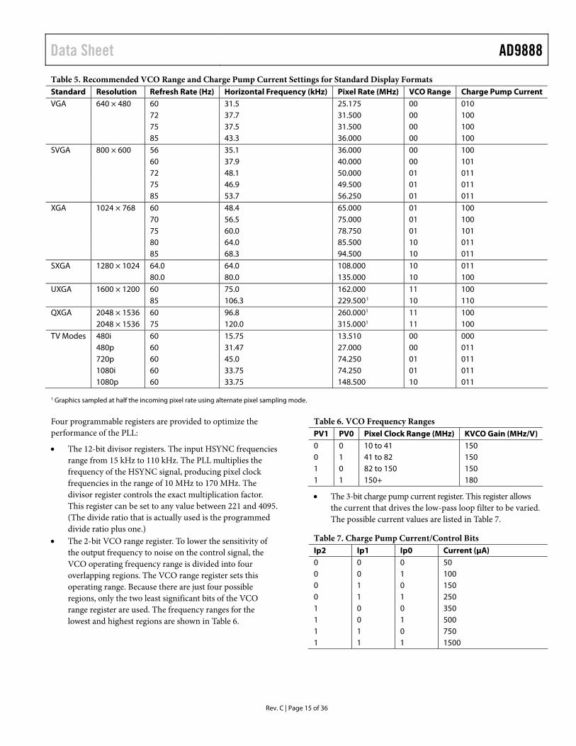
Table 5. Recommended VCO Range and Charge Pump Current Settings for Standard Display Formats Standard Resolution Refresh Rate (Hz) Horizontal Frequency (kHz) Pixel Rate (MHz) VCO Range Charge Pump Current VGA 640 × 480 60 31.5 25.175 00 010 72 37.7 31.500 00 100 75 37.5 31.500 00 100 85 43.3 36.000 00 100 SVGA 800 × 600 56 35.1 36.000 00 100 60 37.9 40.000 00 101 72 48.1 50.000 01 011 75 46.9 49.500 01 011 85 53.7 56.250 01 011 XGA 1024 × 768 60 48.4 65.000 01 100 70 56.5 75.000 01 100 75 60.0 78.750 01 101 80 64.0 85.500 10 011 85 68.3 94.500 10 011 SXGA 1280 × 1024 64.0 64.0 108.000 10 011 80.0 80.0 135.000 10 100 UXGA 1600 × 1200 60 75.0 162.000 11 100 85 106.3 229.5001 10 110 QXGA 2048 × 1536 60 96.8 260.0001 11 100 2048 × 1536 75 120.0 315.0001 11 100 TV Modes 480i 60 15.75 13.510 00 000 480p 60 31.47 27.000 00 011 720p 60 45.0 74.250 01 011 1080i 60 33.75 74.250 01 011 1080p 60 33.75 148.500 10 011 1 Graphics sampled at half the incoming pixel rate using alternate pixel sampling mode.
Four programmable registers are provided to optimize the performance of the PLL:
• The 12-bit divisor registers. The input HSYNC frequencies range from 15 kHz to 110 kHz. The PLL multiplies the frequency of the HSYNC signal, producing pixel clock frequencies in the range of 10 MHz to 170 MHz. The divisor register controls the exact multiplication factor. This register can be set to any value between 221 and 4095. (The divide ratio that is actually used is the programmed divide ratio plus one.)
• The 2-bit VCO range register. To lower the sensitivity of the output frequency to noise on the control signal, the VCO operating frequency range is divided into four overlapping regions. The VCO range register sets this operating range. Because there are just four possible regions, only the two least significant bits of the VCO range register are used. The frequency ranges for the lowest and highest regions are shown in Table 6.
Table 6. VCO Frequency Ranges PV1 PV0 Pixel Clock Range (MHz) KVCO Gain (MHz/V) 0 0 10 to 41 150 0 1 41 to 82 150 1 0 82 to 150 150 1 1 150+ 180
• The 3-bit charge pump current register. This register allows the current that drives the low-pass loop filter to be varied. The possible current values are listed in Table 7.
Table 7. Charge Pump Current/Control Bits Ip2 Ip1 Ip0 Current (μA) 0 0 0 50 0 0 1 100 0 1 0 150 0 1 1 250 1 0 0 350 1 0 1 500 1 1 0 750 1 1 1 1500
AD9888 Data Sheet
Rev. C | Page 16 of 36
• The 5-bit phase adjust register. The phase of the generated sampling clock may be shifted to locate an optimum sampling point within a clock cycle. The phase adjust register provides 32 phase-shift steps of 11.25° each. The HSYNC signal with an identical phase shift is available through the HSOUT pin. Phase adjustment is still available if the pixel clock is being provided externally. The COAST pin is used to allow the PLL to continue to run at the same frequency in the absence of the incoming HSYNC signal. This can be used during the vertical sync period, or any other time that the HSYNC signal is unavailable. The polarity of the COAST signal can be set through the coast polarity register, and the polarity of the HSYNC signal can be set through the HSYNC polarity register.
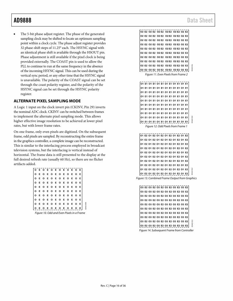
ALTERNATE PIXEL SAMPLING MODE A Logic 1 input on the clock invert pin (CKINV, Pin 29) inverts the nominal ADC clock. CKINV can be switched between frames to implement the alternate pixel sampling mode. This allows higher effective image resolution to be achieved at lower pixel rates, but with lower frame rates.
On one frame, only even pixels are digitized. On the subsequent frame, odd pixels are sampled. By reconstructing the entire frame in the graphics controller, a complete image can be reconstructed. This is similar to the interlacing process employed in broadcast television systems, but the interlacing is vertical instead of horizontal. The frame data is still presented to the display at the full desired refresh rate (usually 60 Hz), so there are no flicker artifacts added.
O E O E O E O E O E O E
O E O E O E O E O E O E
O E O E O E O E O E O E
O E O E O E O E O E O E
O E O E O E O E O E O E
O E O E O E O E O E O E
O E O E O E O E O E O E
O E O E O E O E O E O E
O E O E O E O E O E O E
O E O E O E O E O E O E
0244
2-00
9
Figure 10. Odd and Even Pixels in a Frame
E2 E2 E2 E2
E2 E2 E2 E2
E2 E2 E2 E2
E2 E2 E2 E2
E2 E2 E2 E2
E2 E2 E2 E2
E2 E2 E2 E2
E2 E2 E2 E2
E2 E2 E2 E2
E2 E2 E2 E2
E2
E2
E2
E2
E2
E2
E2
E2
E2
E2
E2
E2
E2
E2
E2
E2
E2
E2
E2
E2
O2
O2
O2
O2
O2
O2
O2
O2
O2
O2
O2
O2
O2
O2
O2
O2
O2
O2
O2
O2
O2
O2
O2
O2
O2
O2
O2
O2
O2
O2
O2
O2
O2
O2
O2
O2
O2
O2
O2
O2
O2
O2
O2
O2
O2
O2
O2
O2
O2
O2
O2
O2
O2
O2
O2
O2
O2
O2
O2
O2
0244
2-01
1
Figure 11. Even Pixels from Frame 2
O1 O1
O1 O1
O1 O1
O1 O1
O1 O1
O1 O1
O1 O1
O1 O1
O1 O1
O1
O1
O1
O1
O1
O1
O1
O1
O1
O1
E1
E1
E1
E1
E1
E1
E1
E1
E1
E1
E1
E1
E1
E1
E1
E1
E1
E1
E1
E1
E1
E1
E1
E1
E1
E1
E1
E1
E1
E1
E1
E1
E1
E1
E1
E1
E1
E1
E1
E1
E1
E1
E1
E1
E1
E1
E1
E1
E1
E1
E1
E1
E1
E1
E1
E1
E1
E1
E1
E1
O1
O1
O1
O1
O1
O1
O1
O1
O1
O1 O1 O1
O1
O1
O1
O1
O1
O1
O1
O1
O1
O1
O1
O1
O1
O1
O1
O1
O1
O1
O1
O1
0244
2-01
0
Figure 12. Odd Pixels from Frame 1
O1 E2 O1 E2 O1 E2 O1 E2 O1 E2 O1 E2
O1 E2 O1 E2 O1 E2 O1 E2 O1 E2 O1 E2
O1 E2 O1 E2 O1 E2 O1 E2 O1 E2 O1 E2
O1 E2 O1 E2 O1 E2 O1 E2 O1 E2 O1 E2
O1 E2 O1 E2 O1 E2 O1 E2 O1 E2 O1 E2
O1 E2 O1 E2 O1 E2 O1 E2 O1 E2 O1 E2
O1 E2 O1 E2 O1 E2 O1 E2 O1 E2 O1 E2
O1 E2 O1 E2 O1 E2 O1 E2 O1 E2 O1 E2
O1 E2 O1 E2 O1 E2 O1 E2 O1 E2 O1 E2
O1 E2 O1 E2 O1 E2 O1 E2 O1 E2 O1 E2
0244
2-01
2
Figure 13. Combined Frame Output from Graphics
O3 E2 O3 E2 O3 E2 O3 E2 O3 E2 O3 E2
O3 E2 O3 E2 O3 E2 O3 E2 O3 E2 O3 E2
O3 E2 O3 E2 O3 E2 O3 E2 O3 E2 O3 E2
O3 E2 O3 E2 O3 E2 O3 E2 O3 E2 O3 E2
O3 E2 O3 E2 O3 E2 O3 E2 O3 E2 O3 E2
O3 E2 O3 E2 O3 E2 O3 E2 O3 E2 O3 E2
O3 E2 O3 E2 O3 E2 O3 E2 O3 E2 O3 E2
O3 E2 O3 E2 O3 E2 O3 E2 O3 E2 O3 E2
O3 E2 O3 E2 O3 E2 O3 E2 O3 E2 O3 E2
O3 E2 O3 E2 O3 E2 O3 E2 O3 E2 O3 E202
442-
013
Figure 14. Subsequent Frame from Controller
Data Sheet AD9888
Rev. C | Page 17 of 36
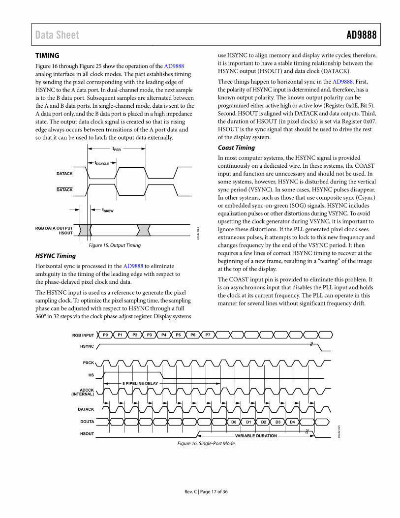
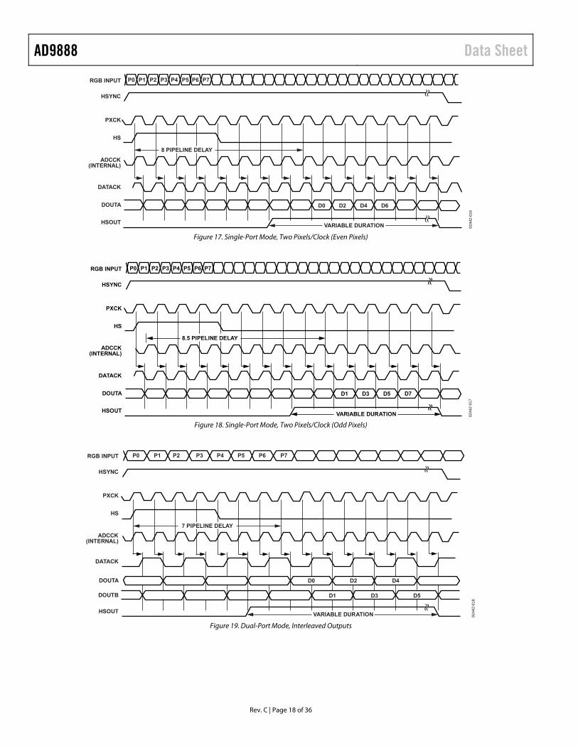
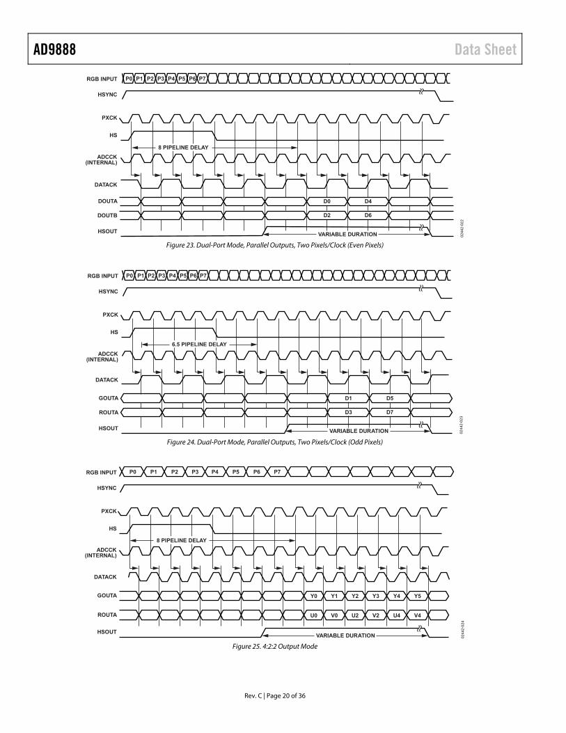
TIMING Figure 16 through Figure 25 show the operation of the AD9888 analog interface in all clock modes. The part establishes timing by sending the pixel corresponding with the leading edge of HSYNC to the A data port. In dual-channel mode, the next sample is to the B data port. Subsequent samples are alternated between the A and B data ports. In single-channel mode, data is sent to the A data port only, and the B data port is placed in a high impedance state. The output data clock signal is created so that its rising edge always occurs between transitions of the A port data and so that it can be used to latch the output data externally.
DATACK
DATACK
RGB DATA OUTPUTHSOUT
tSKEW
tPER
tDCYCLE
0244
2-01
4
Figure 15. Output Timing
HSYNC Timing
Horizontal sync is processed in the AD9888 to eliminate ambiguity in the timing of the leading edge with respect to the phase-delayed pixel clock and data.
The HSYNC input is used as a reference to generate the pixel sampling clock. To optimize the pixel sampling time, the sampling phase can be adjusted with respect to HSYNC through a full 360° in 32 steps via the clock phase adjust register. Display systems
use HSYNC to align memory and display write cycles; therefore, it is important to have a stable timing relationship between the HSYNC output (HSOUT) and data clock (DATACK).
Three things happen to horizontal sync in the AD9888. First, the polarity of HSYNC input is determined and, therefore, has a known output polarity. The known output polarity can be programmed either active high or active low (Register 0x0E, Bit 5). Second, HSOUT is aligned with DATACK and data outputs. Third, the duration of HSOUT (in pixel clocks) is set via Register 0x07. HSOUT is the sync signal that should be used to drive the rest of the display system.
Coast Timing
In most computer systems, the HSYNC signal is provided continuously on a dedicated wire. In these systems, the COAST input and function are unnecessary and should not be used. In some systems, however, HSYNC is disturbed during the vertical sync period (VSYNC). In some cases, HSYNC pulses disappear. In other systems, such as those that use composite sync (Csync) or embedded sync-on-green (SOG) signals, HSYNC includes equalization pulses or other distortions during VSYNC. To avoid upsetting the clock generator during VSYNC, it is important to ignore these distortions. If the PLL generated pixel clock sees extraneous pulses, it attempts to lock to this new frequency and changes frequency by the end of the VSYNC period. It then requires a few lines of correct HSYNC timing to recover at the beginning of a new frame, resulting in a “tearing” of the image at the top of the display.
The COAST input pin is provided to eliminate this problem. It is an asynchronous input that disables the PLL input and holds the clock at its current frequency. The PLL can operate in this manner for several lines without significant frequency drift.
P0 P1 P2 P3 P4 P5 P6 P7
D0 D1 D2 D3 D4
RGB INPUT
HSYNC
PXCK
HS
ADCCK(INTERNAL)
DATACK
DOUTA
HSOUT
8 PIPELINE DELAY
VARIABLE DURATION 0244
2-01
5
Figure 16. Single-Port Mode
AD9888 Data Sheet
Rev. C | Page 18 of 36
P0 P1 P2 P3 P4 P5 P6 P7
D0 D2 D4 D6
RGB INPUT
HSYNC
PXCK
HS
ADCCK(INTERNAL)
DATACK
DOUTA
HSOUT VARIABLE DURATION
8 PIPELINE DELAY
0244
2-01
6
Figure 17. Single-Port Mode, Two Pixels/Clock (Even Pixels)
P0 P1 P2 P3 P4 P5 P6 P7
D1 D3 D5 D7
RGB INPUT
HSYNC
PXCK
HS
ADCCK(INTERNAL)
DATACK
DOUTA
HSOUT
8.5 PIPELINE DELAY
VARIABLE DURATION 0244
2-01
7
Figure 18. Single-Port Mode, Two Pixels/Clock (Odd Pixels)
P0 P1 P2 P3 P4 P5 P6 P7
D0 D2 D4
D1 D3 D5
RGB INPUT
HSYNC
PXCK
HS
ADCCK(INTERNAL)
DATACK
DOUTA
HSOUT
DOUTB
VARIABLE DURATION
7 PIPELINE DELAY
0244
2-01
8
Figure 19. Dual-Port Mode, Interleaved Outputs
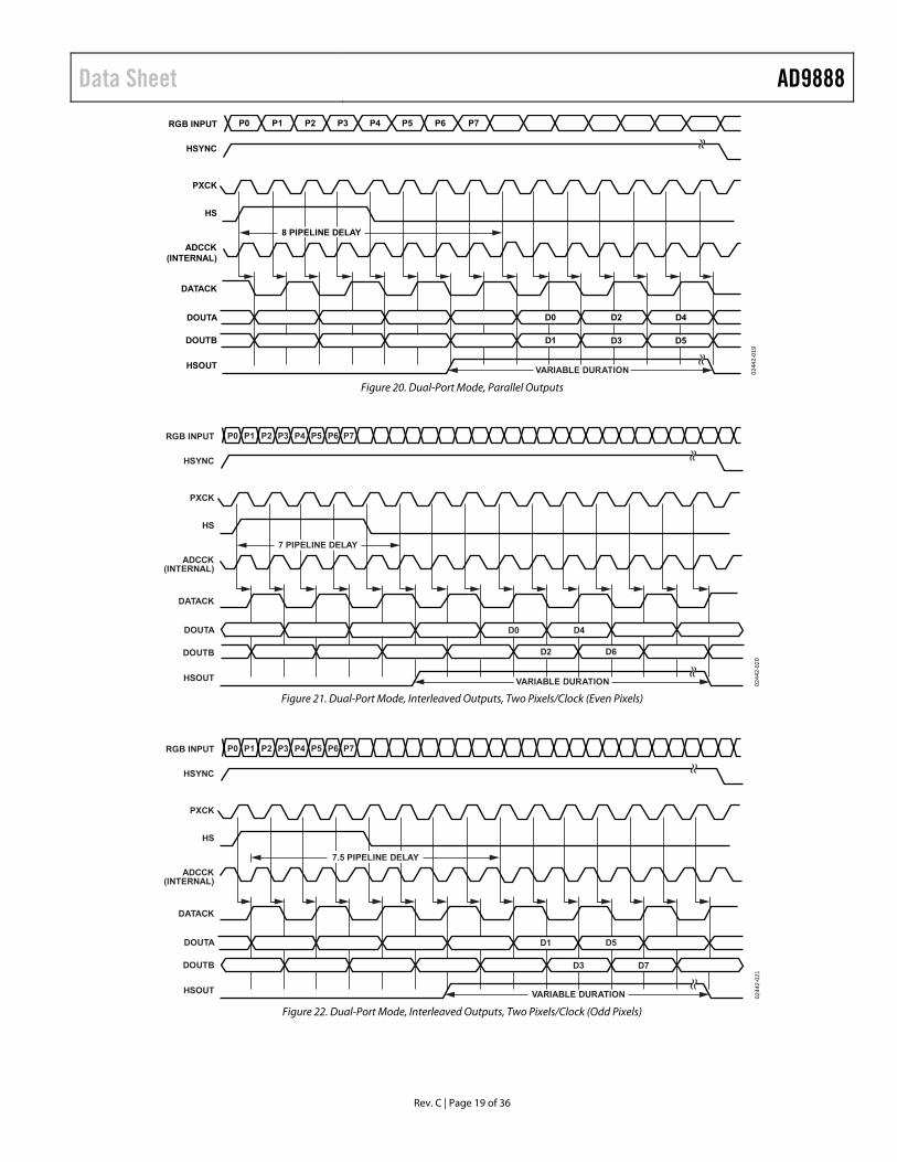
Data Sheet AD9888
Rev. C | Page 19 of 36
P0 P1 P2 P3 P4 P5 P6 P7
D3 D5
RGB INPUT
HSYNC
PXCK
HS
ADCCK(INTERNAL)
DATACK
DOUTA
HSOUT
DOUTB
D0 D2 D4
D1
VARIABLE DURATION
8 PIPELINE DELAY
0244
2-01
9
Figure 20. Dual-Port Mode, Parallel Outputs
P0 P1 P2 P3 P4 P5 P6 P7
D0 D4
D2 D6
RGB INPUT
HSYNC
PXCK
HS
ADCCK(INTERNAL)
DATACK
DOUTA
HSOUT
DOUTB
VARIABLE DURATION
7 PIPELINE DELAY
0244
2-02
0
Figure 21. Dual-Port Mode, Interleaved Outputs, Two Pixels/Clock (Even Pixels)
P0 P1 P2 P3 P4 P5 P6 P7
D3 D7
D1 D5
RGB INPUT
HSYNC
PXCK
HS
ADCCK(INTERNAL)
DATACK
DOUTA
HSOUT
DOUTB
VARIABLE DURATION
7.5 PIPELINE DELAY
0244
2-02
1
Figure 22. Dual-Port Mode, Interleaved Outputs, Two Pixels/Clock (Odd Pixels)
AD9888 Data Sheet
Rev. C | Page 20 of 36
P0 P1 P2 P3 P4 P5 P6 P7
D0
RGB INPUT
HSYNC
PXCK
HS
ADCCK(INTERNAL)
DATACK
DOUTA
HSOUT
DOUTB D2 D6
D4
VARIABLE DURATION
8 PIPELINE DELAY
0244
2-02
2
Figure 23. Dual-Port Mode, Parallel Outputs, Two Pixels/Clock (Even Pixels)
P0 P1 P2 P3 P4 P5 P6 P7
D1 D5
RGB INPUT
HSYNC
PXCK
HS
ADCCK(INTERNAL)
DATACK
GOUTA
HSOUT
ROUTA D3 D7
VARIABLE DURATION
6.5 PIPELINE DELAY
0244
2-02
3
Figure 24. Dual-Port Mode, Parallel Outputs, Two Pixels/Clock (Odd Pixels)
P0 P1 P2 P3 P4 P5 P6 P7
U0 V0 U2 V2 U4
RGB INPUT
HSYNC
PXCK
HS
ADCCK(INTERNAL)
DATACK
ROUTA
HSOUT
Y0 Y1 Y2 Y3 Y4GOUTA
V4
Y5
VARIABLE DURATION
8 PIPELINE DELAY
0244
2-02
4
Figure 25. 4:2:2 Output Mode
Data Sheet AD9888
Rev. C | Page 21 of 36
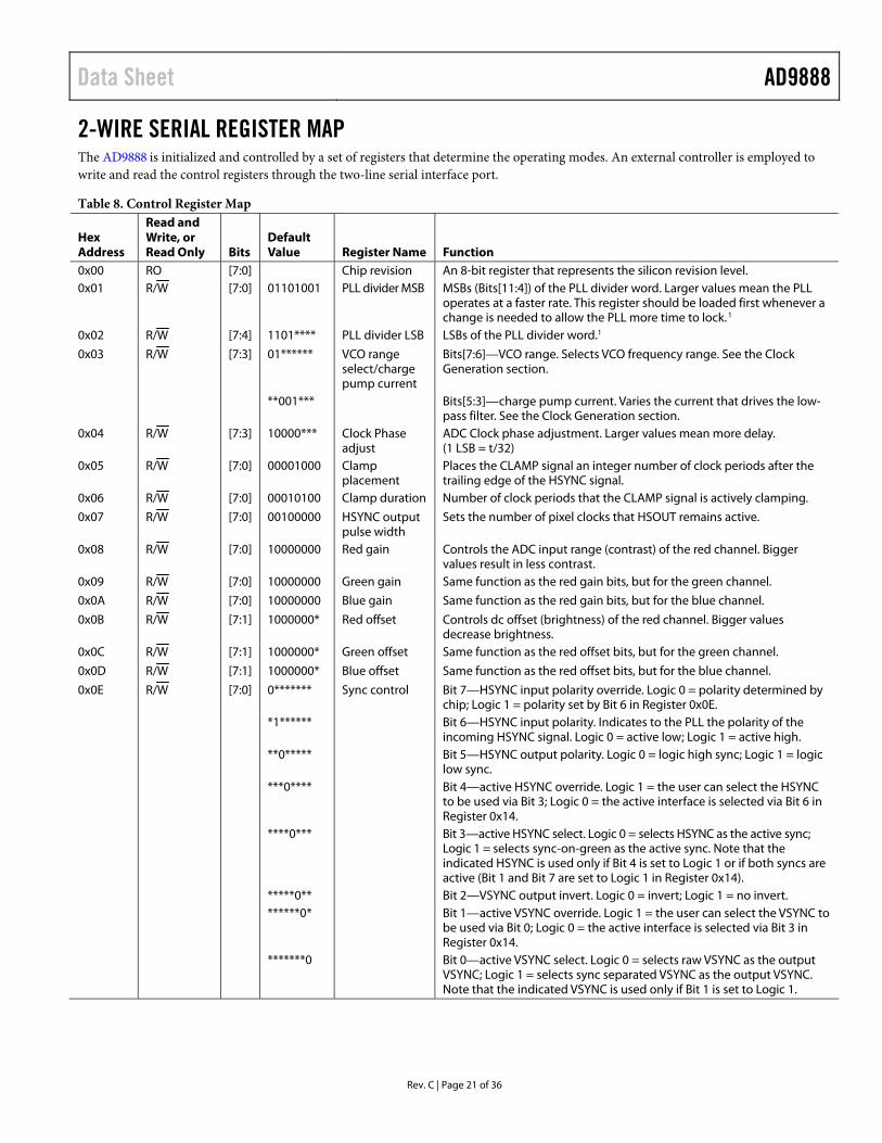
2-WIRE SERIAL REGISTER MAP The AD9888 is initialized and controlled by a set of registers that determine the operating modes. An external controller is employed to write and read the control registers through the two-line serial interface port.
Table 8. Control Register Map
Hex Address
Read and Write, or Read Only Bits
Default Value Register Name Function
0x00 RO [7:0] Chip revision An 8-bit register that represents the silicon revision level. 0x01 R/W [7:0] 01101001 PLL divider MSB MSBs (Bits[11:4]) of the PLL divider word. Larger values mean the PLL
operates at a faster rate. This register should be loaded first whenever a change is needed to allow the PLL more time to lock.1
0x02 R/W [7:4] 1101**** PLL divider LSB LSBs of the PLL divider word.1
0x03 R/W [7:3] 01****** VCO range select/charge pump current
Bits[7:6]—VCO range. Selects VCO frequency range. See the Clock Generation section.
**001*** Bits[5:3]—charge pump current. Varies the current that drives the low-pass filter. See the Clock Generation section.
0x04 R/W [7:3] 10000*** Clock Phase adjust
ADC Clock phase adjustment. Larger values mean more delay. (1 LSB = t/32)
0x05 R/W [7:0] 00001000 Clamp placement
Places the CLAMP signal an integer number of clock periods after the trailing edge of the HSYNC signal.
0x06 R/W [7:0] 00010100 Clamp duration Number of clock periods that the CLAMP signal is actively clamping.
0x07 R/W [7:0] 00100000 HSYNC output pulse width
Sets the number of pixel clocks that HSOUT remains active.
0x08 R/W [7:0] 10000000 Red gain Controls the ADC input range (contrast) of the red channel. Bigger values result in less contrast.
0x09 R/W [7:0] 10000000 Green gain Same function as the red gain bits, but for the green channel.
0x0A R/W [7:0] 10000000 Blue gain Same function as the red gain bits, but for the blue channel.
0x0B R/W [7:1] 1000000* Red offset Controls dc offset (brightness) of the red channel. Bigger values decrease brightness.
0x0C R/W [7:1] 1000000* Green offset Same function as the red offset bits, but for the green channel.
0x0D R/W [7:1] 1000000* Blue offset Same function as the red offset bits, but for the blue channel.
0x0E R/W [7:0] 0******* Sync control Bit 7—HSYNC input polarity override. Logic 0 = polarity determined by chip; Logic 1 = polarity set by Bit 6 in Register 0x0E.
*1****** Bit 6—HSYNC input polarity. Indicates to the PLL the polarity of the incoming HSYNC signal. Logic 0 = active low; Logic 1 = active high.
**0***** Bit 5—HSYNC output polarity. Logic 0 = logic high sync; Logic 1 = logic low sync.
***0**** Bit 4—active HSYNC override. Logic 1 = the user can select the HSYNC to be used via Bit 3; Logic 0 = the active interface is selected via Bit 6 in Register 0x14.
****0*** Bit 3—active HSYNC select. Logic 0 = selects HSYNC as the active sync; Logic 1 = selects sync-on-green as the active sync. Note that the indicated HSYNC is used only if Bit 4 is set to Logic 1 or if both syncs are active (Bit 1 and Bit 7 are set to Logic 1 in Register 0x14).
*****0** Bit 2—VSYNC output invert. Logic 0 = invert; Logic 1 = no invert. ******0* Bit 1—active VSYNC override. Logic 1 = the user can select the VSYNC to
be used via Bit 0; Logic 0 = the active interface is selected via Bit 3 in Register 0x14.
*******0 Bit 0—active VSYNC select. Logic 0 = selects raw VSYNC as the output VSYNC; Logic 1 = selects sync separated VSYNC as the output VSYNC. Note that the indicated VSYNC is used only if Bit 1 is set to Logic 1.
AD9888 Data Sheet
Rev. C | Page 22 of 36
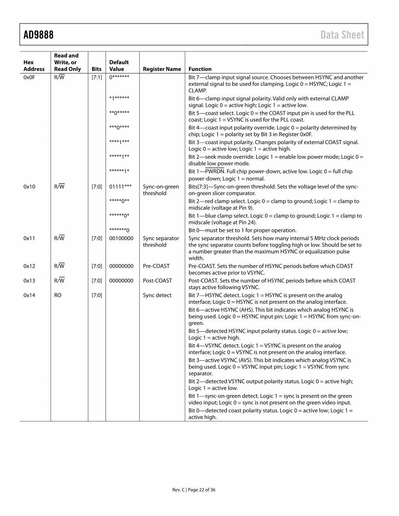
Hex Address
Read and Write, or Read Only Bits
Default Value Register Name Function
0x0F R/W [7:1] 0******* Bit 7—clamp input signal source. Chooses between HSYNC and another external signal to be used for clamping. Logic 0 = HSYNC; Logic 1 = CLAMP.
*1****** Bit 6—clamp input signal polarity. Valid only with external CLAMP signal. Logic 0 = active high; Logic 1 = active low.
**0***** Bit 5—coast select. Logic 0 = the COAST input pin is used for the PLL coast; Logic 1 = VSYNC is used for the PLL coast.
***0**** Bit 4—coast input polarity override. Logic 0 = polarity determined by chip; Logic 1 = polarity set by Bit 3 in Register 0x0F.
****1*** Bit 3—coast input polarity. Changes polarity of external COAST signal. Logic 0 = active low; Logic 1 = active high.
*****1** Bit 2—seek mode override. Logic 1 = enable low power mode; Logic 0 = disable low power mode.
******1* Bit 1—PWRDN. Full chip power-down, active low. Logic 0 = full chip power-down; Logic 1 = normal.
0x10 R/W [7:0] 01111*** Sync-on-green threshold
Bits[7:3]—Sync-on-green threshold. Sets the voltage level of the sync-on-green slicer comparator.
*****0** Bit 2—red clamp select. Logic 0 = clamp to ground; Logic 1 = clamp to midscale (voltage at Pin 9).
******0* Bit 1—blue clamp select. Logic 0 = clamp to ground; Logic 1 = clamp to midscale (voltage at Pin 24).
*******0 Bit 0—must be set to 1 for proper operation. 0x11 R/W [7:0] 00100000 Sync separator
threshold Sync separator threshold. Sets how many internal 5 MHz clock periods the sync separator counts before toggling high or low. Should be set to a number greater than the maximum HSYNC or equalization pulse width.
0x12 R/W [7:0] 00000000 Pre-COAST Pre-COAST. Sets the number of HSYNC periods before which COAST becomes active prior to VSYNC.
0x13 R/W [7:0] 00000000 Post-COAST Post-COAST. Sets the number of HSYNC periods before which COAST stays active following VSYNC.
0x14 RO [7:0] Sync detect Bit 7—HSYNC detect. Logic 1 = HSYNC is present on the analog interface; Logic 0 = HSYNC is not present on the analog interface.
Bit 6—active HSYNC (AHS). This bit indicates which analog HSYNC is being used. Logic 0 = HSYNC input pin; Logic 1 = HSYNC from sync-on-green.
Bit 5—detected HSYNC input polarity status. Logic 0 = active low; Logic 1 = active high.
Bit 4—VSYNC detect. Logic 1 = VSYNC is present on the analog interface; Logic 0 = VSYNC is not present on the analog interface.
Bit 3—active VSYNC (AVS). This bit indicates which analog VSYNC is being used. Logic 0 = VSYNC input pin; Logic 1 = VSYNC from sync separator.
Bit 2—detected VSYNC output polarity status. Logic 0 = active high; Logic 1 = active low.
Bit 1—sync-on-green detect. Logic 1 = sync is present on the green video input; Logic 0 = sync is not present on the green video input.
Bit 0—detected coast polarity status. Logic 0 = active low; Logic 1 = active high.
Data Sheet AD9888
Rev. C | Page 23 of 36
Hex Address
Read and Write, or Read Only Bits
Default Value Register Name Function
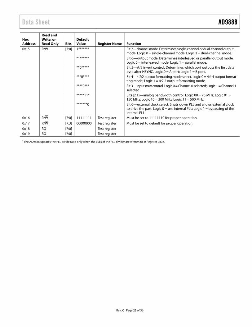
0x15 R/W [7:0] 1******* Bit 7—channel mode. Determines single-channel or dual-channel output mode. Logic 0 = single-channel mode; Logic 1 = dual-channel mode.
*1****** Bit 6—output mode. Determines interleaved or parallel output mode. Logic 0 = interleaved mode; Logic 1 = parallel mode.
**0***** Bit 5—A/B invert control. Determines which port outputs the first data byte after HSYNC. Logic 0 = A port; Logic 1 = B port.
***0**** Bit 4—4:2:2 output formatting mode select. Logic 0 = 4:4:4 output format-ting mode; Logic 1 = 4:2:2 output formatting mode.
****0*** Bit 3—input mux control. Logic 0 = Channel 0 selected; Logic 1 = Channel 1 selected
*****11* Bits [2:1]—analog bandwidth control. Logic 00 = 75 MHz; Logic 01 = 150 MHz; Logic 10 = 300 MHz; Logic 11 = 500 MHz.
*******0 Bit 0—external clock select. Shuts down PLL and allows external clock to drive the part. Logic 0 = use internal PLL; Logic 1 = bypassing of the internal PLL.
0x16 R/W [7:0] 11111111 Test register Must be set to 11111110 for proper operation.
0x17 R/W [7:3] 00000000 Test register Must be set to default for proper operation.
0x18 RO [7:0] Test register 0x19 RO [7:0] Test register 1 The AD9888 updates the PLL divide ratio only when the LSBs of the PLL divider are written to in Register 0x02.
AD9888 Data Sheet
Rev. C | Page 24 of 36
2-WIRE SERIAL CONTROL REGISTER DETAILS CHIP IDENTIFICATION Address 0x00[7:0]—Chip Revision
An 8-bit register that represents the silicon revision.
PLL DIVIDER CONTROL Address 0x01[7:0]—PLL Divide Ratio MSBs
The eight MSBs of the 12-bit PLL divide ratio (PLLDIV). The operational divide ratio is PLLDIV + 1.
The PLL derives a master clock from an incoming HSYNC signal. The master clock frequency is then divided by an integer value, such that the output is phase locked to HSYNC. This PLLDIV value determines the number of pixel times (pixels plus horizontal blanking overhead) per line. This is typically 20% to 30% more than the number of active pixels in the display.
The 12-bit value of the PLL divider supports divide ratios from 2 to 4095. The higher the value loaded in this register, the higher the resulting clock frequency with respect to a fixed HSYNC frequency.
VESA has established standard timing specifications that assist in determining the value for PLLDIV as a function of horizontal and vertical display resolution and frame rate (see Table 5). However, many computer systems do not conform precisely to the recom-mendations, and these numbers should be used only as a guide. The display system manufacturer should provide automatic or manual means for optimizing PLLDIV. An incorrectly set PLLDIV usually produces one or more vertical noise bars on the display. The greater the error, the greater the number of bars produced.
The power-up default value of PLLDIV is 1693 (PLLDIVM = 0x69, PLLDIVL = 0xDx).
The AD9888 updates the full divide ratio only when the LSBs are changed. Writing to this register by itself does not trigger an update.
Address 0x02[7:4]—PLL Divide Ratio LSBs
The four LSBs of the 12-bit PLL divide ratio (PLLDIV). The operational divide ratio is PLLDIV + 1.
The power-up default value of PLLDIV is 1693 (PLLDIVM = 0x69, PLLDIVL = 0xDx).
The AD9888 updates the full divide ratio only when this register is written to.
CLOCK GENERATOR CONTROL Address 0x03[7:6]—VCO Range Select
Two bits that establish the operating range of the clock generator.
The VCO range must be set to correspond with the desired operating frequency (incoming pixel rate).
The PLL provides the best jitter performance at high frequencies. To output low pixel rates while minimizing jitter, the PLL operates at a higher frequency and then divides down the clock rate after-wards. Table 9 shows the pixel rates for each VCO range setting.
The PLL output divisor is automatically selected with the VCO range setting.
Table 9. VCO Ranges Settings VCO Range Select Setting Data Clock Range (MHz) 00 10 to 41 01 (default) 41 to 82 10 82 to 150 11 150+
Address 0x03[5:3]—Charge Pump Current
Three bits that establish the current driving the loop filter in the clock generator. These bits must be set to correspond with the desired operating frequency (incoming pixel rate).
Table 10. Charge Pump Current Settings Charge Pump Current Setting Current (mA) 000 50 001 (default) 100 010 150 011 250 100 350 101 500 110 750 111 1500
Address 0x04[7:3]—Clock Phase Adjust
A 5-bit value that adjusts the sampling phase in 32 steps across one pixel time. Each step represents an 11.25° shift in sampling phase.
The power-up default value is 16.
CLAMP TIMING Address 0x05[7:0]—Clamp Placement
An 8-bit register that sets the position of the internally generated clamp.
When the external clamp control bit is set to 0, a CLAMP signal is generated internally after the trailing edge of HSYNC at a position (in pixel periods) established by the clamp placement bits and for a duration (in pixel periods) set by the clamp duration bits. The clamp placement can be programmed to any value up to 255, except 0.
The clamp should be placed during a time when the input signal presents a stable black level reference, usually the back porch period between HSYNC and the image.
When the external clamp control bit is set to 1, this register is ignored.
Address 0x06[7:0]—Clamp Duration
An 8-bit register that sets the duration of the internally generated clamp.
When the external clamp control bit is set to 0, a CLAMP signal is generated internally after the trailing edge of HSYNC at a position

Data Sheet AD9888
Rev. C | Page 25 of 36
(in pixel periods) established by the clamp placement bits and for a duration (in pixel periods) set by the clamp duration bits. The clamp duration can be programmed to any value between 1 and 255. A value of 0 is not supported.
For the best results, the clamp duration should be set to include the majority of the black reference signal time that follows the HSYNC signal trailing edge. Insufficient clamping time can produce brightness changes at the top of the screen and a slow recovery from large changes in the average picture level (APL), or brightness.
When the external clamp control bit is set to 1, this register is ignored.
HSYNC PULSE WIDTH Address 0x07[7:0]—HSYNC Output Pulse Width
An 8-bit register that sets the duration of the HSYNC output pulse.
The leading edge of the HSYNC output is triggered by the internally generated, phase-adjusted PLL feedback clock. The AD9888 then counts a number of pixel clocks equal to the value in this register. This triggers the trailing edge of the HSYNC output, which is also phase adjusted.
INPUT GAIN Address 0x08[7:0]—Red Channel Gain Adjust (Red Gain)
An 8-bit word that sets the gain of the red channel.
The AD9888 can accommodate input signals with a full-scale range between 0.5 V p-p and 1.0 V p-p. Setting red gain to 255 corres-ponds to an input range of 1.0 V p-p. A red gain of 0 establishes an input range of 0.5 V p-p. Note that increasing red gain results in the picture having less contrast because the input signal uses fewer of the available converter codes (see Figure 5). The same functionality also applies to the green and blue channel gain adjust bits.
Address 0x09[7:0]—Green Channel Gain Adjust (Green Gain)
An 8-bit word that sets the gain of the green channel (see the Address 0x08[7:0]—Red Channel Gain Adjust (Red Gain) section for more information).
Address 0x0A[7:0]—Blue Channel Gain Adjust (Blue Gain)
An 8-bit word that sets the gain of the blue channel (see the Address 0x08[7:0]—Red Channel Gain Adjust (Red Gain) section for more information).
INPUT OFFSET Address 0x0B[7:1]—Red Channel Offset Adjust (Red Offset)
A 7-bit offset binary word that sets the dc offset of the red channel.
One LSB of offset adjustment equals approximately one LSB change in the ADC offset. Therefore, the absolute magnitude of the offset
adjustment scales as the gain of the channel changes. A nominal setting of 63 results in the channel nominally clamping to Code 00 during the back porch clamping interval. An offset setting of 127 results in the channel clamping to Code 64 of the ADC. An offset setting of 0 clamps to Code −63. Increasing the value of red offset decreases the brightness of the channel. The same functionality also applies to the green and blue channel offset adjust bits.
Address 0x0C[7:1]—Green Channel Offset Adjust (Green Offset)
A 7-bit offset binary word that sets the dc offset of the green channel (see the Address 0x0B[7:1]—Red Channel Offset Adjust (Red Offset) section for more information).
Address 0x0D[7:1]—Blue Channel Offset Adjust (Blue Offset)
A 7-bit offset binary word that sets the dc offset of the blue channel (see the Address 0x0B[7:1]—Red Channel Offset Adjust (Red Offset) section for more information).
SYNC CONTROL Address 0x0E[7]—HSYNC Input Polarity Override
This register is used to override the internal circuitry that determines the polarity of the HSYNC signal going into the PLL.
Table 11. HSYNC Input Polarity Override Settings HSYNC Input Polarity Override Setting Function 0 (default) HSYNC polarity is determined by chip. 1 HSYNC polarity is determined by user.
Address 0x0E[6]—HSYNC Input Polarity
This bit must be set to indicate the polarity of the HSYNC signal that is applied to the PLL HSYNC input.
Table 12. HSYNC Input Polarity Settings HSYNC Input Polarity Setting Function 0 Active low 1 (default) Active high
Active low means that the leading edge of the HSYNC pulse is negative-going and, therefore, timing is based on the leading edge of HSYNC, which is the falling edge. The rising edge has no effect.
Active high means that the leading edge of the HSYNC pulse is positive-going and, therefore, timing is based on the leading edge of HSYNC, which is the rising edge.
Although the device can operate if this bit is set incorrectly, the internally generated clamp position, as established by the clamp placement (Register 0x05), will not be placed as expected, which may generate clamping errors.
AD9888 Data Sheet
Rev. C | Page 26 of 36
Address 0x0E[5]—HSYNC Output Polarity
This bit determines the polarity of the HSYNC output and the SOG output (see Table 13).
Table 13. HSYNC Output Polarity Settings HSYNC Output Polarity Setting Function 0 (default) Logic 1 (positive polarity) 1 Logic 0 (negative polarity)
Address 0x0E[4]—Active HSYNC Override
This bit is used to override the automatic HSYNC selection. To initiate this override, set this bit to Logic 1. When overriding the automatic HSYNC selection, the active HSYNC is set via Bit 3 in this register.
Table 14. Active HSYNC Override Settings Active HSYNC Override Setting Function 0 (default) Bit 6 in Register 0x14 deter-
mines the active interface. 1 Override, Bit 3 determines
the active interface.
Address 0x0E[3]—Active HSYNC Select
This bit is used under two conditions. It is used to select the active HSYNC when the override bit (Register 0x0E, Bit 4) is set. Alternatively, it is used to determine the active HSYNC when the override bit is not set but both HSYNCs are detected.
Table 15. Active HSYNC Select Settings Active HSYNC Select Setting Function 0 (default) HSYNC input 1 Sync-on-green input
Address 0x0E[2]—VSYNC Output Invert
This bit inverts the polarity of the VSYNC output (see Table 16).
Table 16. VSYNC Output Polarity Settings VSYNC Output Invert Setting Function 0 (default) Invert 1 Do not invert
Address 0x0E[1]—Active VSYNC Override
This bit is used to override the automatic VSYNC selection. To initiate this override, set this bit to Logic 1. When overriding the automatic VSYNC selection, the active interface is set via Bit 0 in this register.
Table 17. Active VSYNC Override Settings Active VSYNC Override Setting Function 0 (default) Bit 3 in Register 0x14 deter-
mines the active VSYNC. 1 Override, Bit 0 determines
the active VSYNC.
Address 0x0E[0]—Active VSYNC Select
This bit is used to select the active VSYNC when the override bit (Register 0x0E, Bit 1) is set.
Table 18. Active VSYNC Select Settings Active VSYNC Select Setting Function 0 (default) VSYNC input 1 Sync separator output
INPUT CONTROL Address 0x0F[7]—Clamp Input Signal Source
This bit determines the source of clamp timing.
Table 19. Clamp Input Signal Source Settings Clamp Input Signal Source Setting Function 0 (default) Internally generated
clamp 1 Externally provided
clamp signal
A 0 enables the clamp timing circuitry controlled by clamp placement and clamp duration. The clamp position and duration is counted from the trailing edge of HSYNC.
A 1 enables the external CLAMP input pin. The three channels are clamped when the CLAMP signal is active. The polarity of CLAMP is determined by the clamp input signal polarity bit (Register 0x0F, Bit 6).
Address 0x0F[6]—Clamp Input Signal Polarity
This bit determines the polarity of the externally provided CLAMP signal.
Table 20. Clamp Input Signal Polarity Settings CLAMP Input Signal Polarity Setting Function 0 Active high 1 (default) Active low
A Logic 1 means the circuit clamps when CLAMP is low and passes the signal to the ADC when CLAMP is high.
A Logic 0 means the circuit clamps when CLAMP is high and passes the signal to the ADC when CLAMP is low.
Address 0x0F[5]—Coast Select
This bit is used to select the active coast source. The choices are the COAST input pin or VSYNC. If VSYNC is selected, users must decide whether to use the VSYNC input pin or the output from the sync separator (Register 0x0E, Bit 1 and Bit 0).
Table 21. Coast Source Selection Settings Coast Select Setting Function 0 (default) COAST input pin 1 VSYNC (must choose
VSYNC input pin or output from sync separator)
Data Sheet AD9888
Rev. C | Page 27 of 36
Address 0x0F[4]—Coast Input Polarity Override
This bit is used to override the internal circuitry that determines the polarity of the COAST signal going into the PLL.
Table 22. Coast Input Polarity Override Settings Coast Input Polarity Override Setting Function 0 (default) Coast polarity is determined by chip. 1 Coast polarity is determined by user.
Address 0x0F[3]—Coast Input Polarity
This bit indicates the polarity of the COAST signal that is applied to the PLL coast input.
Table 23. Coast Input Polarity Settings Coast Input Polarity Setting Function 0 Active low 1 (default) Active high
Active low means that the clock generator ignores HSYNC inputs when COAST is low and continues operating at the same nominal frequency until COAST goes high.
Active high means that the clock generator ignores HSYNC inputs when COAST is high and continues operating at the same nominal frequency until COAST goes low.
This function needs to be used along with the coast polarity override bit (Bit 4).
Address 0x0F[2]—Seek Mode Override
This bit is used to either enable or disable the low power mode. The low power mode (seek mode) occurs when there are no signals on any of the sync inputs.
Table 24. Seek Mode Override Settings Seek Mode Override Setting Function 0 Disable seek mode 1 (default) Enable seek mode
Address 0x0F[1]—PWRDN
This bit is used to put the chip into power-down mode. In this mode, the power dissipation of the chip is reduced to a fraction of the typical power (see the specifications in Table 1 for exact power dissipation). When the chip is in power-down mode, the HSOUT, VSOUT, DATACK, DATACK, and all 48 of the data outputs are put into a high impedance state. Note that the SOGOUT output is not put into high impedance. Circuit blocks that continue to be active during power-down mode include the voltage references, sync processing, sync detection, and the serial register. These blocks facilitate a fast startup from power-down.
Table 25. PWRDN Settings PWRDN Setting Function 0 Power-down 1 (default) Normal operation
Address 0x10[7:3]—Sync-on-Green Slicer Threshold
These bits allow the comparator threshold of the sync-on-green slicer to be adjusted. The threshold can be adjusted in steps of 10 mV, with a minimum setting of 10 mV and a maximum setting of 330 mV.
The default setting is 01111, which corresponds to a threshold value of 0.16 V.
Address 0x10[2]—Red Clamp Select
This bit determines whether the red channel is clamped to ground or to midscale. For RGB video, all three channels are referenced to ground. For YCbCr (or YUV), the Y channel is referenced to ground, but the CbCr channels are referenced to midscale. Clamping to midscale clamps to Pin 9.
Table 26. Red Clamp Select Settings Red Clamp Select Setting Function 0 (default) Clamp to ground 1 Clamp to midscale (Pin 9)
Address 0x10[1]—Blue Clamp Select
This bit determines whether the blue channel is clamped to ground or to midscale. Clamping to midscale clamps to Pin 24.
Table 27. Blue Clamp Select Settings Blue Clamp Select Setting Function 0 (default) Clamp to ground 1 Clamp to midscale (Pin 24)
Address 0x11[7:0]—Sync Separator Threshold
These bits are used to set the responsiveness of the sync separator. The bits set how many internal 5 MHz clock periods the sync separator must count before toggling high or low. This functions like a low-pass filter to ignore HSYNC pulses to extract the VSYNC signal. The bits should be set to a number greater than the maxi-mum HSYNC pulse width. The sync separator threshold uses an internal dedicated clock with a frequency of approximately 5 MHz.
The default for this register is 0x20.
Address 0x12[7:0]—Pre-COAST
These bits allow the COAST signal to be applied prior to the VSYNC signal. This is necessary in cases where preequali zation pulses are present. The step size for this control is one HSYNC period.
The default is 0.
Address 0x13[7:0]—Post-COAST
This register allows the COAST signal to be applied after the VSYNC signal. This is necessary in cases where postequali-zation pulses are present. The step size for this control is one HSYNC period.
The default setting for each of these bits is 0.
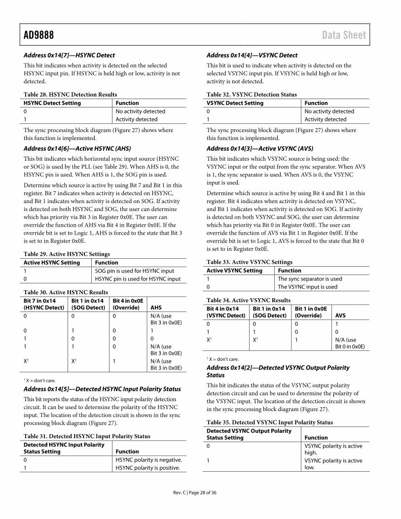
AD9888 Data Sheet
Rev. C | Page 28 of 36
Address 0x14[7]—HSYNC Detect
This bit indicates when activity is detected on the selected HSYNC input pin. If HSYNC is held high or low, activity is not detected.
Table 28. HSYNC Detection Results HSYNC Detect Setting Function 0 No activity detected 1 Activity detected
The sync processing block diagram (Figure 27) shows where this function is implemented.
Address 0x14[6]—Active HSYNC (AHS)
This bit indicates which horizontal sync input source (HSYNC or SOG) is used by the PLL (see Table 29). When AHS is 0, the HSYNC pin is used. When AHS is 1, the SOG pin is used.
Determine which source is active by using Bit 7 and Bit 1 in this register. Bit 7 indicates when activity is detected on HSYNC, and Bit 1 indicates when activity is detected on SOG. If activity is detected on both HSYNC and SOG, the user can determine which has priority via Bit 3 in Register 0x0E. The user can override the function of AHS via Bit 4 in Register 0x0E. If the override bit is set to Logic 1, AHS is forced to the state that Bit 3 is set to in Register 0x0E.
Table 29. Active HSYNC Settings Active HSYNC Setting Function 1 SOG pin is used for HSYNC input 0 HSYNC pin is used for HSYNC input
Table 30. Active HSYNC Results Bit 7 in 0x14 (HSYNC Detect)
Bit 1 in 0x14 (SOG Detect)
Bit 4 in 0x0E (Override) AHS
0 0 0 N/A (use Bit 3 in 0x0E)
0 1 0 1 1 0 0 0 1 1 0 N/A (use
Bit 3 in 0x0E) X1 X1 1 N/A (use
Bit 3 in 0x0E) 1 X = don’t care.
Address 0x14[5]—Detected HSYNC Input Polarity Status
This bit reports the status of the HSYNC input polarity detection circuit. It can be used to determine the polarity of the HSYNC input. The location of the detection circuit is shown in the sync processing block diagram (Figure 27).
Table 31. Detected HSYNC Input Polarity Status Detected HSYNC Input Polarity Status Setting Function 0 HSYNC polarity is negative. 1 HSYNC polarity is positive.
Address 0x14[4]—VSYNC Detect
This bit is used to indicate when activity is detected on the selected VSYNC input pin. If VSYNC is held high or low, activity is not detected.
Table 32. VSYNC Detection Status VSYNC Detect Setting Function 0 No activity detected 1 Activity detected
The sync processing block diagram (Figure 27) shows where this function is implemented.
Address 0x14[3]—Active VSYNC (AVS)
This bit indicates which VSYNC source is being used: the VSYNC input or the output from the sync separator. When AVS is 1, the sync separator is used. When AVS is 0, the VSYNC input is used.
Determine which source is active by using Bit 4 and Bit 1 in this register. Bit 4 indicates when activity is detected on VSYNC, and Bit 1 indicates when activity is detected on SOG. If activity is detected on both VSYNC and SOG, the user can determine which has priority via Bit 0 in Register 0x0E. The user can override the function of AVS via Bit 1 in Register 0x0E. If the override bit is set to Logic 1, AVS is forced to the state that Bit 0 is set to in Register 0x0E.
Table 33. Active VSYNC Settings Active VSYNC Setting Function 1 The sync separator is used 0 The VSYNC input is used
Table 34. Active VSYNC Results Bit 4 in 0x14 (VSYNC Detect)
Bit 1 in 0x14 (SOG Detect)
Bit 1 in 0x0E (Override) AVS
0 0 0 1 1 1 0 0 X1 X1 1 N/A (use
Bit 0 in 0x0E) 1 X = don’t care.
Address 0x14[2]—Detected VSYNC Output Polarity Status
This bit indicates the status of the VSYNC output polarity detection circuit and can be used to determine the polarity of the VSYNC input. The location of the detection circuit is shown in the sync processing block diagram (Figure 27).
Table 35. Detected VSYNC Input Polarity Status Detected VSYNC Output Polarity Status Setting Function 0 VSYNC polarity is active
high. 1 VSYNC polarity is active
low.
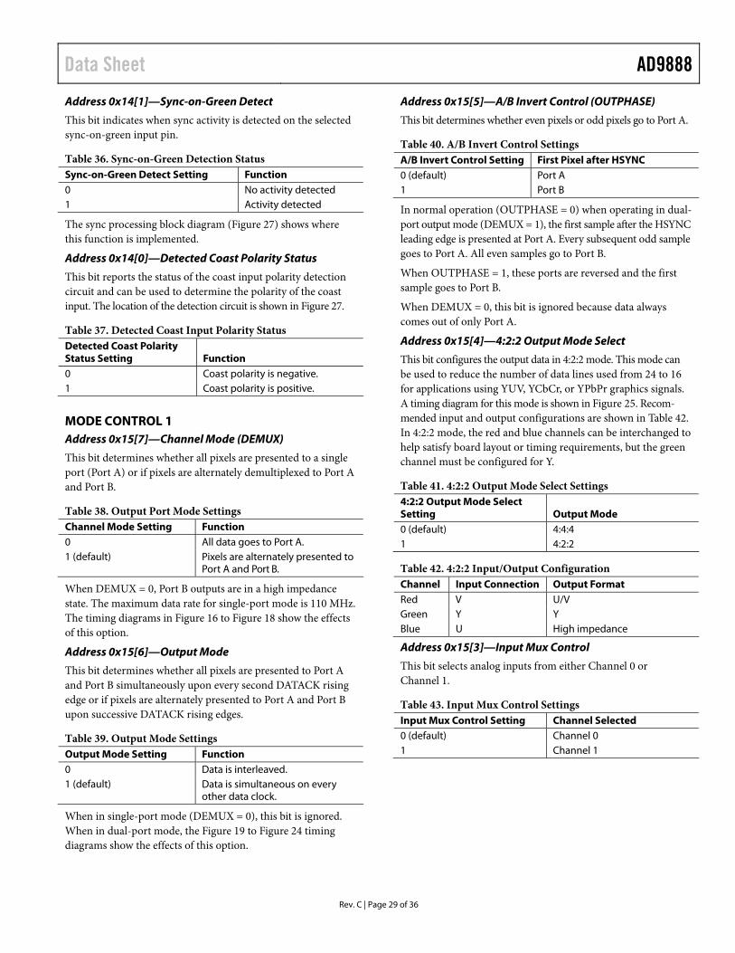
Data Sheet AD9888
Rev. C | Page 29 of 36
Address 0x14[1]—Sync-on-Green Detect
This bit indicates when sync activity is detected on the selected sync-on-green input pin.
Table 36. Sync-on-Green Detection Status Sync-on-Green Detect Setting Function 0 No activity detected 1 Activity detected
The sync processing block diagram (Figure 27) shows where this function is implemented.
Address 0x14[0]—Detected Coast Polarity Status
This bit reports the status of the coast input polarity detection circuit and can be used to determine the polarity of the coast input. The location of the detection circuit is shown in Figure 27.
Table 37. Detected Coast Input Polarity Status Detected Coast Polarity Status Setting Function 0 Coast polarity is negative. 1 Coast polarity is positive.
MODE CONTROL 1 Address 0x15[7]—Channel Mode (DEMUX)
This bit determines whether all pixels are presented to a single port (Port A) or if pixels are alternately demultiplexed to Port A and Port B.
Table 38. Output Port Mode Settings Channel Mode Setting Function 0 All data goes to Port A. 1 (default) Pixels are alternately presented to
Port A and Port B.
When DEMUX = 0, Port B outputs are in a high impedance state. The maximum data rate for single-port mode is 110 MHz. The timing diagrams in Figure 16 to Figure 18 show the effects of this option.
Address 0x15[6]—Output Mode
This bit determines whether all pixels are presented to Port A and Port B simultaneously upon every second DATACK rising edge or if pixels are alternately presented to Port A and Port B upon successive DATACK rising edges.
Table 39. Output Mode Settings Output Mode Setting Function 0 Data is interleaved. 1 (default) Data is simultaneous on every
other data clock.
When in single-port mode (DEMUX = 0), this bit is ignored. When in dual-port mode, the Figure 19 to Figure 24 timing diagrams show the effects of this option.
Address 0x15[5]—A/B Invert Control (OUTPHASE)
This bit determines whether even pixels or odd pixels go to Port A.
Table 40. A/B Invert Control Settings A/B Invert Control Setting First Pixel after HSYNC 0 (default) Port A 1 Port B
In normal operation (OUTPHASE = 0) when operating in dual-port output mode (DEMUX = 1), the first sample after the HSYNC leading edge is presented at Port A. Every subsequent odd sample goes to Port A. All even samples go to Port B.
When OUTPHASE = 1, these ports are reversed and the first sample goes to Port B.
When DEMUX = 0, this bit is ignored because data always comes out of only Port A.
Address 0x15[4]—4:2:2 Output Mode Select
This bit configures the output data in 4:2:2 mode. This mode can be used to reduce the number of data lines used from 24 to 16 for applications using YUV, YCbCr, or YPbPr graphics signals. A timing diagram for this mode is shown in Figure 25. Recom-mended input and output configurations are shown in Table 42. In 4:2:2 mode, the red and blue channels can be interchanged to help satisfy board layout or timing requirements, but the green channel must be configured for Y.
Table 41. 4:2:2 Output Mode Select Settings 4:2:2 Output Mode Select Setting Output Mode 0 (default) 4:4:4 1 4:2:2
Table 42. 4:2:2 Input/Output Configuration Channel Input Connection Output Format Red V U/V Green Y Y Blue U High impedance
Address 0x15[3]—Input Mux Control
This bit selects analog inputs from either Channel 0 or Channel 1.
Table 43. Input Mux Control Settings Input Mux Control Setting Channel Selected 0 (default) Channel 0 1 Channel 1
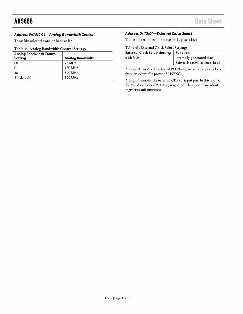
AD9888 Data Sheet
Rev. C | Page 30 of 36
Address 0x15[2:1]—Analog Bandwidth Control
These bits select the analog bandwidth.
Table 44. Analog Bandwidth Control Settings Analog Bandwidth Control Setting Analog Bandwidth 00 75 MHz 01 150 MHz 10 300 MHz 11 (default) 500 MHz
Address 0x15[0]—External Clock Select
This bit determines the source of the pixel clock.
Table 45. External Clock Select Settings External Clock Select Setting Function 0 (default) Internally generated clock 1 Externally provided clock signal
A Logic 0 enables the internal PLL that generates the pixel clock from an externally provided HSYNC.
A Logic 1 enables the external CKEXT input pin. In this mode, the PLL divide ratio (PLLDIV) is ignored. The clock phase adjust register is still functional.
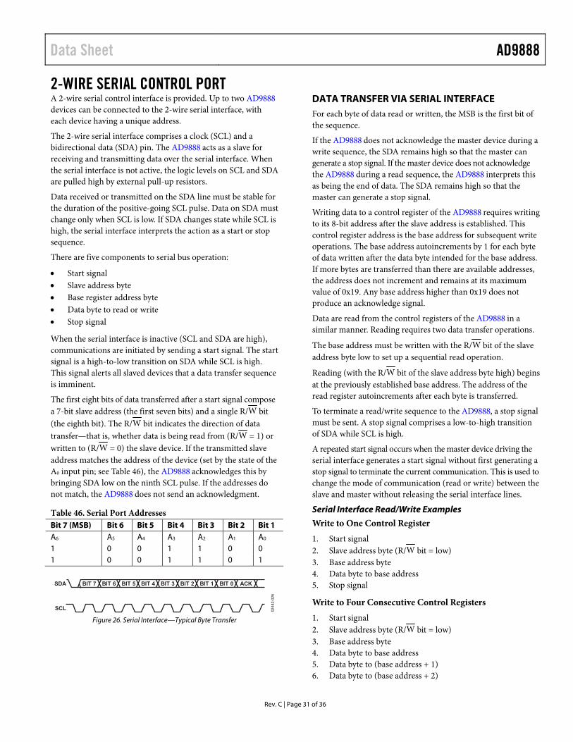
Data Sheet AD9888
Rev. C | Page 31 of 36
2-WIRE SERIAL CONTROL PORT A 2-wire serial control interface is provided. Up to two AD9888 devices can be connected to the 2-wire serial interface, with each device having a unique address.
The 2-wire serial interface comprises a clock (SCL) and a bidirectional data (SDA) pin. The AD9888 acts as a slave for receiving and transmitting data over the serial interface. When the serial interface is not active, the logic levels on SCL and SDA are pulled high by external pull-up resistors.
Data received or transmitted on the SDA line must be stable for the duration of the positive-going SCL pulse. Data on SDA must change only when SCL is low. If SDA changes state while SCL is high, the serial interface interprets the action as a start or stop sequence.
There are five components to serial bus operation:
• Start signal • Slave address byte • Base register address byte • Data byte to read or write • Stop signal
When the serial interface is inactive (SCL and SDA are high), communications are initiated by sending a start signal. The start signal is a high-to-low transition on SDA while SCL is high. This signal alerts all slaved devices that a data transfer sequence is imminent.
The first eight bits of data transferred after a start signal compose a 7-bit slave address (the first seven bits) and a single R/W bit (the eighth bit). The R/W bit indicates the direction of data transfer—that is, whether data is being read from (R/W = 1) or written to (R/W = 0) the slave device. If the transmitted slave address matches the address of the device (set by the state of the A0 input pin; see ), the acknowledges this by bringing SDA low on the ninth SCL pulse. If the addresses do not match, the does not send an acknowledgment.
Table 46 AD9888
AD9888
Table 46. Serial Port Addresses Bit 7 (MSB) Bit 6 Bit 5 Bit 4 Bit 3 Bit 2 Bit 1 A6 A5 A4 A3 A2 A1 A0 1 0 0 1 1 0 0 1 0 0 1 1 0 1
BIT 7SDA
SCL
ACKBIT 6 BIT 5 BIT 4 BIT 3 BIT 2 BIT 1 BIT 0
0244
2-02
6
Figure 26. Serial Interface—Typical Byte Transfer
DATA TRANSFER VIA SERIAL INTERFACE For each byte of data read or written, the MSB is the first bit of the sequence.
If the AD9888 does not acknowledge the master device during a write sequence, the SDA remains high so that the master can generate a stop signal. If the master device does not acknowledge the AD9888 during a read sequence, the AD9888 interprets this as being the end of data. The SDA remains high so that the master can generate a stop signal.
Writing data to a control register of the AD9888 requires writing to its 8-bit address after the slave address is established. This control register address is the base address for subsequent write operations. The base address autoincrements by 1 for each byte of data written after the data byte intended for the base address. If more bytes are transferred than there are available addresses, the address does not increment and remains at its maximum value of 0x19. Any base address higher than 0x19 does not produce an acknowledge signal.
Data are read from the control registers of the AD9888 in a similar manner. Reading requires two data transfer operations.
The base address must be written with the R/W bit of the slave address byte low to set up a sequential read operation.
Reading (with the R/W bit of the slave address byte high) begins at the previously established base address. The address of the read register autoincrements after each byte is transferred.
To terminate a read/write sequence to the AD9888, a stop signal must be sent. A stop signal comprises a low-to-high transition of SDA while SCL is high.
A repeated start signal occurs when the master device driving the serial interface generates a start signal without first generating a stop signal to terminate the current communication. This is used to change the mode of communication (read or write) between the slave and master without releasing the serial interface lines.
Serial Interface Read/Write Examples
Write to One Control Register
1. Start signal 2. Slave address byte (R/W bit = low) 3. Base address byte 4. Data byte to base address 5. Stop signal
Write to Four Consecutive Control Registers
1. Start signal 2. Slave address byte (R/W bit = low) 3. Base address byte 4. Data byte to base address 5. Data byte to (base address + 1) 6. Data byte to (base address + 2)
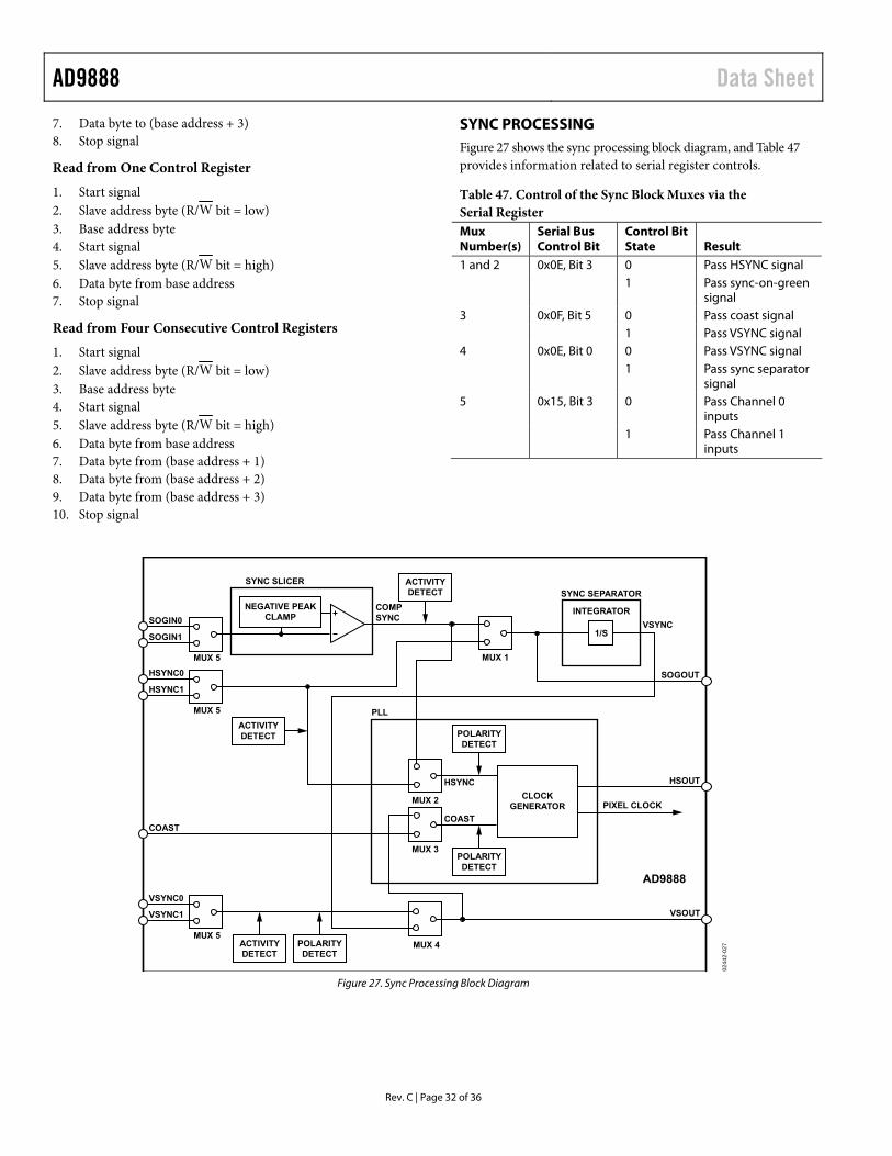
AD9888 Data Sheet
Rev. C | Page 32 of 36
7. Data byte to (base address + 3) 8. Stop signal
Read from One Control Register
1. Start signal 2. Slave address byte (R/W bit = low) 3. Base address byte 4. Start signal 5. Slave address byte (R/W bit = high) 6. Data byte from base address 7. Stop signal
Read from Four Consecutive Control Registers
1. Start signal 2. Slave address byte (R/W bit = low) 3. Base address byte 4. Start signal 5. Slave address byte (R/W bit = high) 6. Data byte from base address 7. Data byte from (base address + 1) 8. Data byte from (base address + 2) 9. Data byte from (base address + 3) 10. Stop signal
SYNC PROCESSING Figure 27 shows the sync processing block diagram, and Table 47 provides information related to serial register controls.
Table 47. Control of the Sync Block Muxes via the Serial Register Mux Number(s)
Serial Bus Control Bit
Control Bit State Result
1 and 2 0x0E, Bit 3 0 Pass HSYNC signal 1 Pass sync-on-green
signal 3 0x0F, Bit 5 0 Pass coast signal 1 Pass VSYNC signal 4 0x0E, Bit 0 0 Pass VSYNC signal 1 Pass sync separator
signal 5 0x15, Bit 3 0 Pass Channel 0
inputs 1 Pass Channel 1
inputs
SYNC SLICER
NEGATIVE PEAKCLAMP
COMPSYNCSOGIN0
HSYNC0
PIXEL CLOCK
MUX 1
SYNC SEPARATOR
INTEGRATORVSYNC
SOGOUT
HSOUT
VSOUT
MUX 4
1/S
PLL
HSYNC
ACTIVITYDETECT
AD9888
CLOCKGENERATOR
COASTCOAST
HSYNC1
SOGIN1
ACTIVITYDETECT
ACTIVITYDETECT
POLARITYDETECT
POLARITYDETECT
POLARITYDETECT
MUX 2
MUX 3
MUX 5
MUX 5
VSYNC0
VSYNC1
MUX 5
0244
2-02
7
Figure 27. Sync Processing Block Diagram
Data Sheet AD9888
Rev. C | Page 33 of 36
SYNC SLICER The purpose of the sync slicer is to extract the sync signal from the green graphics channel. A sync signal is not present on all graphics signals, only those with sync-on-green. The sync signal is extracted from the green channel in a two-step process. First, the SOG input is clamped to its negative peak (typically 0.3 V below the black level). Next, the signal goes to a comparator with a variable trigger level, nominally 0.15 V above the clamped level. The “sliced” sync is typically a composite sync signal containing both HSYNC and VSYNC.
SYNC SEPARATOR A sync separator extracts the VSYNC signal from a composite sync signal by using a low-pass filter-like or integrator-like operation. It works on the idea that the VSYNC signal stays active for a much longer time than the HSYNC signal. Therefore, the sync separator rejects any signal shorter than a threshold value, which is some-where between an HSYNC pulse width and a VSYNC pulse width.
The sync separator on the AD9888 is an 8-bit digital counter with a 5 MHz clock. It works independently of the polarity of the composite sync signal. Polarities are determined elsewhere on the chip. The basic idea is that the counter counts up when
HSYNC pulses are present. Because HSYNC pulses are relatively short in width, the counter only reaches a value of N before the pulse ends. It then starts counting down, eventually reaching 0 before the next HSYNC pulse arrives. The specific value of N varies among video modes, but is always less than 255. For example, with a 1 μs width HSYNC, the counter reaches only 5 (1 μs/200 ns = 5). When VSYNC is present on the composite sync, the counter also counts up. However, because the VSYNC signal is much longer, the counter reaches a higher number, M. For most video modes, M is at least 255. Therefore, VSYNC can be detected on the composite sync signal by detecting when the counter counts to higher than N. The specific count that triggers detection (T) can be programmed through the serial register (Address 0x0F).
After VSYNC is detected, there is a similar process to detect when it becomes inactive. Upon detection, the counter first resets to 0, and then starts counting up when VSYNC disappears. Similar to the previous case, the sync separator detects the absence of VSYNC when the counter reaches the threshold count (T). In this way, the sync separator rejects noise and/or serration pulses. After VSYNC is detected to be absent, the counter resets to 0 and begins the cycle again.
AD9888 Data Sheet
Rev. C | Page 34 of 36
PCB LAYOUT RECOMMENDATIONS The AD9888 is a high precision, high speed analog device. To optimize its performance, it is important to have a well laid out board. This section provides guidelines for designing a board using the AD9888.
ANALOG INTERFACE INPUTS Using the following layout techniques on the graphics inputs is extremely important.
Minimize the trace length running into the graphics inputs by placing the AD9888 as close as possible to the graphics (VGA) connector. Long input trace lengths are undesirable because they pick up more noise from the board and other external sources.
Place the 75 Ω termination resistors (see Figure 4) as close as possible to the AD9888 chip. Any additional trace length between the termination resistors and the input of the AD9888 increases the magnitude of reflections, which corrupts the graphics signal.
Use 75 Ω matched impedance traces. Trace impedances other than 75 Ω increase the chance of reflections.
The AD9888 has very high input bandwidth (500 MHz). Although this is desirable for acquiring a high resolution PC graphics signal with fast edges, it means that the device also captures any high frequency noise present. Therefore, it is important to reduce the amount of noise coupled to the inputs. Avoid running any digital traces near the analog inputs.
The AD9888 can digitize graphics signals over a very wide range of frequencies (10 MHz to 170 MHz). Often, characteristics that are beneficial at one frequency can be detrimental at another. Analog bandwidth is one such characteristic. For UXGA resolutions (up to 170 MHz), a very high analog bandwidth is desirable because of the fast input signal slew rates. For VGA and lower resolutions (down to 12.5 MHz), a very high bandwidth is not desirable because it allows excess noise to pass through. To accommodate these varying needs, the AD9888 includes variable analog bandwidth control. Four settings are available (75 MHz, 150 MHz, 300 MHz, and 500 MHz), allowing the analog bandwidth to be matched with the resolution of the incoming graphics signal.
POWER SUPPLY BYPASSING It is recommended to bypass each power supply pin with a 0.1 μF capacitor. The exception is when two or more supply pins are adjacent to each other. For these groupings of powers/ grounds, it is necessary to have only one bypass capacitor. The fundamental idea is to have a bypass capacitor within about 0.5 cm of each power pin. In addition, avoid placing the capacitor on the side of the PC board opposite from the AD9888 because this interposes resistive vias in the path.
The bypass capacitors should be physically located between the power plane and the power pin. Current should flow from the power plane to the capacitor to the power pin. Do not make the power connection between the capacitor and the power pin.
Placing a via underneath the capacitor pads, down to the power plane, is generally the best approach.
It is particularly important to maintain low noise and good stability of PVD (the PLL, VCO supply). Abrupt changes in PVD can result in similarly abrupt changes in sampling clock phase and frequency. This can be avoided by careful regulation, filtering, and bypassing. It is highly desirable to provide separate, regulated supplies for each of the analog circuitry groups, VD and PVD.
Some graphics controllers use substantially different levels of power when active (during active picture time) and when idle (during horizontal and vertical sync periods). This can result in a measurable change in the voltage supplied to the analog supply regulator, which can in turn produce changes in the regulated analog supply voltage. This can be mitigated by regulating the analog supply, or at least PVD, from a different, cleaner power source, for example, from a 12 V supply.
It is also recommended to use a single ground plane for the entire board. Experience shows that the noise performance is the same or better with a single ground plane. Using multiple ground planes can be detrimental because each separate ground plane is smaller, and long ground loops can result.
In some cases, using separate ground planes is unavoidable. For these cases, it is recommended to at least place a single ground plane under the AD9888. The location of the split should be at the receiver of the digital outputs, making it even more important to place components wisely because the current loops will be much longer, and current takes the path of least resistance. The following is an example of a current loop signal path: power plane to AD9888 to digital output trace to digital data receiver to digital ground plane to analog ground plane.
PLL Place the PLL loop filter components as close as possible to the FILT pin. Do not place any digital or other high frequency trace near these components. Use the values suggested in the data sheet with 10% tolerances or less.
OUTPUTS (BOTH DATA AND CLOCKS) Try to minimize the trace length that the digital outputs must drive. Longer traces have higher capacitance, requiring more current and causing more internal digital noise. Shorter traces reduce the possibility of reflections.
Adding a series resistor with a value of 22 Ω to 100 Ω can suppress reflections, reduce EMI, and reduce the current spikes inside the AD9888. However, if 50 Ω traces are used on the PCB, the data output should not need these resistors.
A 22 Ω resistor on the DATACK output should provide good impedance matching that reduces reflections. If series resistors are used, place them as close as possible to the AD9888 pins, but avoid adding vias or extra length to the output trace.
Data Sheet AD9888
Rev. C | Page 35 of 36
If possible, limit the capacitance that each of the digital outputs drives to less than 10 pF. This can easily be accomplished by keeping traces short and connecting the outputs to only one device. Loading the outputs with excessive capacitance increases the current transients inside of the AD9888, creating more digital noise on its power supplies.
DIGITAL INPUTS The digital inputs on the AD9888 were designed to work with 3.3 V signals, but are tolerant of 5.0 V signals. Therefore, no extra components are needed when using 5.0 V logic.
Any noise in the HSYNC input trace produces jitter in the system. Therefore, minimize the trace length, and do not run any digital or other high frequency trace near it.
VOLTAGE REFERENCE The voltage reference should be bypassed with a 0.1 μF capacitor. Place it as close as possible to the REF BYPASS pin. Make the ground connection as short as possible.
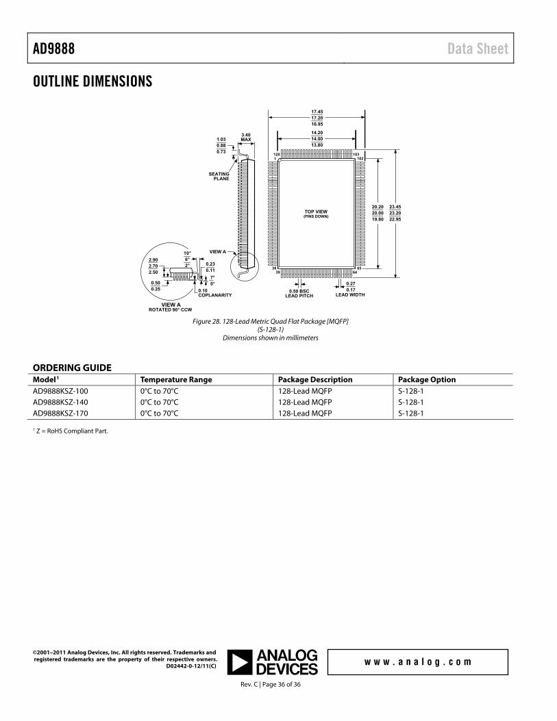
AD9888 Data Sheet
Rev. C | Page 36 of 36
OUTLINE DIMENSIONS
TOP VIEW(PINS DOWN)
1
3839
6564
102128 103
0.270.170.50 BSC
LEAD PITCH
1.030.880.73
SEATINGPLANE
3.40MAX
17.4517.2016.95
14.2014.0013.80
20.2020.0019.80
23.4523.2022.95
VIEW A2.902.702.50
0.500.25
7°0°
0.10COPLANARITY
VIEW AROTATED 90° CCW
10°6°2° 0.23
0.11
LEAD WIDTH
Figure 28. 128-Lead Metric Quad Flat Package [MQFP]
(S-128-1) Dimensions shown in millimeters
ORDERING GUIDE Model1 Temperature Range Package Description Package Option AD9888KSZ-100 0°C to 70°C 128-Lead MQFP S-128-1 AD9888KSZ-140 0°C to 70°C 128-Lead MQFP S-128-1 AD9888KSZ-170 0°C to 70°C 128-Lead MQFP S-128-1 1 Z = RoHS Compliant Part.
©2001–2011 Analog Devices, Inc. All rights reserved. Trademarks and registered trademarks are the property of their respective owners. D02442-0-12/11(C)
Related Documents