www.ti.com FEATURES DESCRIPTION 1 2 3 4 5 6 7 8 9 10 20 19 18 17 16 15 14 13 12 11 A0 A1 A2 A3 A4 A5 A6 A7 A8 GND V CC EOC I/O CLOCK ADDRESS DATA OUT CS REF+ REF- A10 A9 DB, DW, J, OR N PACKAGE (TOP VIEW) 3 2 1 20 19 9 10 11 12 13 4 5 6 7 8 18 17 16 15 14 I/O CLOCK ADDRESS DATA OUT CS REF+ A3 A4 A5 A6 A7 FK OR FN PACKAGE (TOP VIEW) A2 A1 A0 A10 REF - EOC A8 GND A9 V CC TLC1542I, TLC1542M, TLC1542Q TLC1542C, TLC1543C, TLC1543I, TLC1543Q SLAS052G – MARCH 1992 – REVISED JANUARY 2006 10-BIT ANALOG-TO-DIGITAL CONVERTERS WITH SERIAL CONTROL AND 11 ANALOG INPUTS • 10-Bit Resolution A/D Converter • 11 Analog Input Channels • Three Built-In Self-Test Modes • Inherent Sample-and-Hold Function • Total Unadjusted Error: ±1LSB Max • On-Chip System Clock • End-of-Conversion (EOC) Output • Terminal Compatible With TLC542 • CMOS Technology The TLC1542C, TLC1542I, TLC1542M, TLC1542Q, TLC1543C, TLC1543I, and TLC1543Q are CMOS 10-bit switched-capacitor successive-approximation analog-to-digital converters. These devices have three inputs and a 3-state output [chip select (CS), input-output clock (I/O CLOCK), address input (ADDRESS), and data output (DATA OUT)] that provide a direct 4-wire interface to the serial port of a host processor. These devices allow high-speed data transfers from the host. In addition to a high-speed A/D converter and versatile control capability, these devices have an on-chip 14-channel multiplexer that can select any one of 11 analog inputs or any one of three internal self-test voltages. The sample-and-hold function is automatic. At the end of A/D conversion, the end-of-conversion (EOC) output goes high to indicate that conversion is complete. The converter incorporated in the devices features differential high-impedance reference inputs that facilitate ratiometric conversion, scaling, and isolation of analog circuitry from logic and supply noise. A switched-capacitor design allows low-error conversion over the full operating free-air temperature range. Please be aware that an important notice concerning availability, standard warranty, and use in critical applications of Texas Instruments semiconductor products and disclaimers thereto appears at the end of this data sheet. PRODUCTION DATA information is current as of publication date. Copyright © 1992–2006, Texas Instruments Incorporated Products conform to specifications per the terms of the Texas Instruments standard warranty. Production processing does not necessarily include testing of all parameters.

Welcome message from author
This document is posted to help you gain knowledge. Please leave a comment to let me know what you think about it! Share it to your friends and learn new things together.
Transcript
www.ti.com
FEATURES
DESCRIPTION
1
2
3
4
5
6
7
8
9
10
20
19
18
17
16
15
14
13
12
11
A0A1A2A3A4A5A6A7A8
GND
VCC
EOCI/O CLOCKADDRESSDATA OUTCSREF+REF−A10A9
DB, DW, J, OR N PACKAGE(TOP VIEW)
3 2 1 20 19
9 10 11 12 13
4
5
6
7
8
18
17
16
15
14
I/O CLOCKADDRESSDATA OUTCSREF+
A3A4A5A6A7
FK OR FN PACKAGE(TOP VIEW)
A2
A1
A0
A10
RE
F −
EO
C
A8
GN
D A9
VC
C
TLC1542I,, TLC1542M,, TLC1542QTLC1542C, TLC1543C, TLC1543I, TLC1543Q
SLAS052G–MARCH 1992–REVISED JANUARY 2006
10-BIT ANALOG-TO-DIGITAL CONVERTERSWITH SERIAL CONTROL AND 11 ANALOG INPUTS
• 10-Bit Resolution A/D Converter• 11 Analog Input Channels• Three Built-In Self-Test Modes• Inherent Sample-and-Hold Function• Total Unadjusted Error: ±1LSB Max• On-Chip System Clock• End-of-Conversion (EOC) Output• Terminal Compatible With TLC542• CMOS Technology
The TLC1542C, TLC1542I, TLC1542M, TLC1542Q,TLC1543C, TLC1543I, and TLC1543Q are CMOS10-bit switched-capacitor successive-approximationanalog-to-digital converters. These devices havethree inputs and a 3-state output [chip select (CS),input-output clock (I/O CLOCK), address input(ADDRESS), and data output (DATA OUT)] thatprovide a direct 4-wire interface to the serial port of ahost processor. These devices allow high-speed datatransfers from the host.
In addition to a high-speed A/D converter andversatile control capability, these devices have anon-chip 14-channel multiplexer that can select anyone of 11 analog inputs or any one of three internalself-test voltages. The sample-and-hold function isautomatic. At the end of A/D conversion, theend-of-conversion (EOC) output goes high toindicate that conversion is complete. The converterincorporated in the devices features differentialhigh-impedance reference inputs that facilitateratiometric conversion, scaling, and isolation ofanalog circuitry from logic and supply noise. Aswitched-capacitor design allows low-errorconversion over the full operating free-airtemperature range.
Please be aware that an important notice concerning availability, standard warranty, and use in critical applications of TexasInstruments semiconductor products and disclaimers thereto appears at the end of this data sheet.
PRODUCTION DATA information is current as of publication date. Copyright © 1992–2006, Texas Instruments IncorporatedProducts conform to specifications per the terms of the TexasInstruments standard warranty. Production processing does notnecessarily include testing of all parameters.
www.ti.com
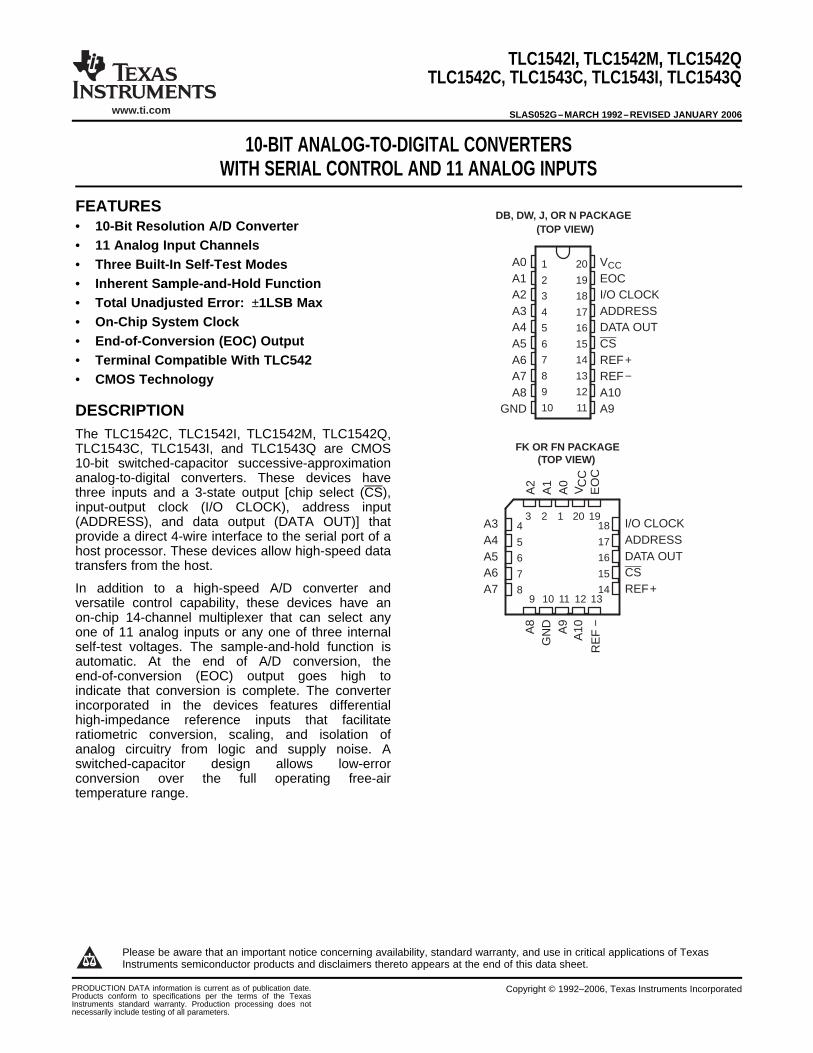
14-ChannelAnalog
Multiplexer
4
10
10
4
REF+ REF−
DATAOUT
ADDRESS
I/O CLOCK
CS
3
EOC
A0
A1
A2A3
A4A5A6
A7A8
A9
A10
1
2
34
567
89
11
12
18
15
17
19
16
14 13
10-BitAnalog-to-Digital
Converter(switched capacitors)
Sample andHold
Input AddressRegister
Self-TestReference
OutputData
Register
System Clock,Control Logic,
and I/OCounters
10-to-1 DataSelector and
Driver
TYPICAL EQUIVALENT INPUTS
INPUT CIRCUIT IMPEDANCE DURING SAMPLING MODE INPUT CIRCUIT IMPEDANCE DURING HOLD MODE1 kΩ TYP
Ci = 60 pF TYP(equivalent inputcapacitance)
5 MΩ TYP
A0−A10 A0−A10
TLC1542I,, TLC1542M,, TLC1542QTLC1542C, TLC1543C, TLC1543I, TLC1543Q
SLAS052G–MARCH 1992–REVISED JANUARY 2006
These devices have limited built-in ESD protection. The leads should be shorted together or the device placed in conductive foamduring storage or handling to prevent electrostatic damage to the MOS gates.
AVAILABLE OPTIONS
PACKAGE
SMALLTA SMALL OUTLINE CHIP CARRIER PLASTIC DIP CHIP CARRIER CERAMIC DIPOUTLINE (DW) (FN) (N) (FK) (J)(DB)
TLC1542CDW TLC1542CFN TLC1542CN0°C to 70°C
TLC1543CDB TLC1543CDW TLC1543CFN TLC1543CN
TLC1542IDW TLC1542IFN TLC1542IN-40°C to 85°C
TLC1543IDB TLC1543IDW TLC1543IFN TLC1543IN
TLC1542QFN-40°C to 125°C
TLC1543QDB TLC1543QDW TLC1543QFN
-55°C to 125°C TLC1542MFK TLC1542MJ
FUNCTIONAL BLOCK DIAGRAM
2 Submit Documentation Feedback
www.ti.com
DETAILED DESCRIPTION
TLC1542I,, TLC1542M,, TLC1542QTLC1542C, TLC1543C, TLC1543I, TLC1543Q
SLAS052G–MARCH 1992–REVISED JANUARY 2006
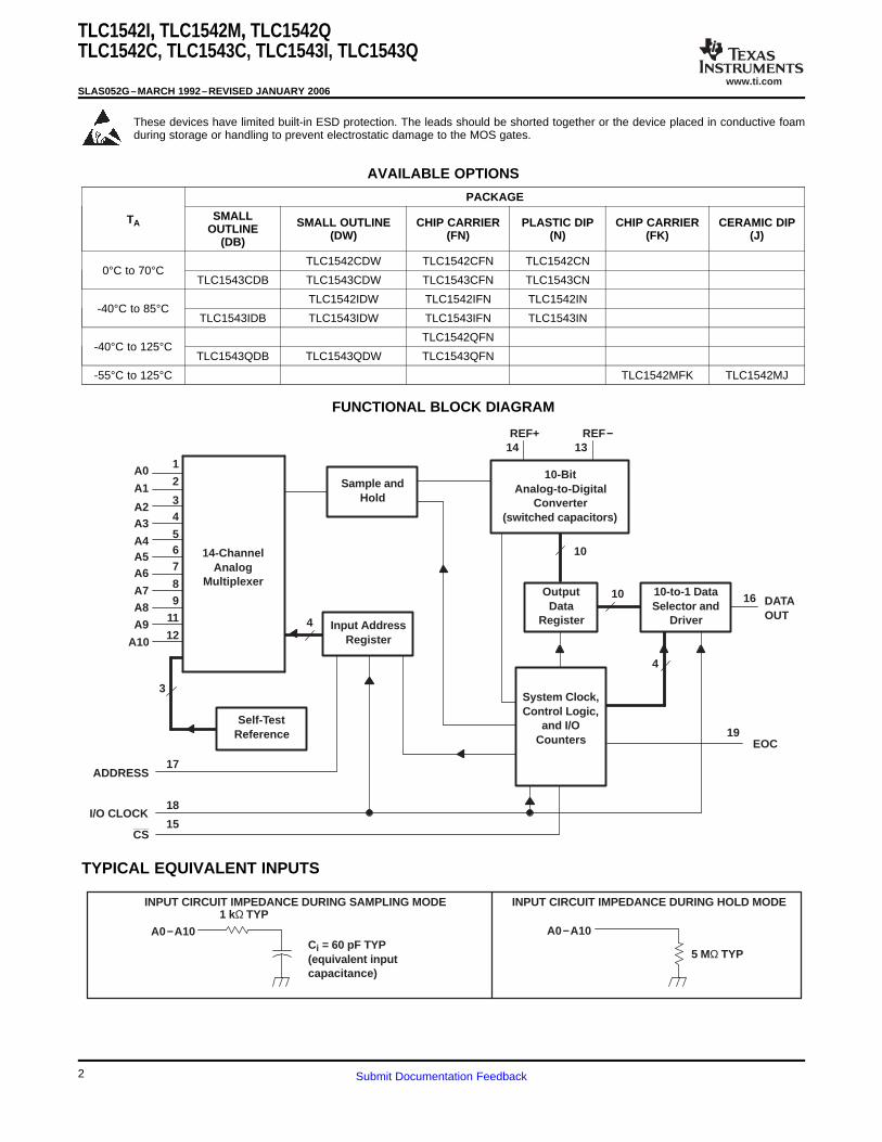
TERMINAL FUNCTIONS
TERMINALI/O DESCRIPTION
NAME NO.
ADDRESS 17 I Serial address input. A 4-bit serial address selects the desired analog input or test voltage that is to beconverted next. The address data is presented with the MSB first and shifts in on the first four risingedges of I/O CLOCK. After the four address bits have been read into the address register, this input isignored for the remainder of the current conversion period.
A0-A10 1-9, 11, 12 I Analog signal inputs. The 11 analog inputs are applied to these terminals and are internallymultiplexed. The driving source impedance should be less than or equal to 1 kΩ.
CS 15 I Chip select. A high-to-low transition on this input resets the internal counters and controls and enablesDATA OUT, ADDRESS, and I/O CLOCK within a maximum of a setup time plus two falling edges ofthe internal system clock. A low-to-high transition disables ADDRESS and I/O CLOCK within a setuptime plus two falling edges of the internal system clock.
DATA OUT 16 O The 3-state serial output for the A/D conversion result. This output is in the high-impedance statewhen CS is high and active when CS is low. With a valid chip select, DATA OUT is removed from thehigh-impedance state and is driven to the logic level corresponding to the MSB value of the previousconversion result. The next falling edge of I/O CLOCK drives this output to the logic levelcorresponding to the next most significant bit, and the remaining bits shift out in order with the LSBappearing on the ninth falling edge of I/O CLOCK. On the tenth falling edge of I/O CLOCK, DATAOUT is driven to a low logic level so that serial interface data transfers of more than ten clocksproduce zeroes as the unused LSBs.
EOC 19 O End of conversion. This output goes from a high to a low logic level on the trailing edge of the tenthI/O CLOCK and remains low until the conversion is complete and data are ready for transfer.
GND 10 I The ground return terminal for the internal circuitry. Unless otherwise noted, all voltage measurementsare with respect to this terminal.
I/O CLOCK 18 I Input/output clock. This terminal receives the serial I/O CLOCK input and performs the following fourfunctions: 1) It clocks the four input address bits into the address register on the first four rising edgesof the I/O CLOCK with the multiplex address available after the fourth rising edge. 2) On the fourthfalling edge of I/O CLOCK, the analog input voltage on the selected multiplex input begins chargingthe capacitor array and continues to do so until the tenth falling edge of I/O CLOCK. 3) It shifts thenine remaining bits of the previous conversion data out on DATA OUT. 4) It transfers control of theconversion to the internal state controller on the falling edge of the tenth clock.
REF+ 14 I The upper reference voltage value (nominally VCC) is applied to this terminal. The maximum inputvoltage range is determined by the difference between the voltage applied to this terminal and thevoltage applied to the REF- terminal.
REF- 13 I The lower reference voltage value (nominally ground) is applied to this terminal.
VCC 20 I Positive supply voltage
With chip select (CS) inactive (high), the ADDRESS and I/O CLOCK inputs are initially disabled and DATA OUTis in the high-impedance state. When the serial interface takes CS active (low), the conversion sequence beginswith the enabling of I/O CLOCK and ADDRESS and the removal of DATA OUT from the high-impedance state.The serial interface then provides the 4-bit channel address to ADDRESS and the I/O CLOCK sequence to I/OCLOCK. During this transfer, the serial interface also receives the previous conversion result from DATA OUT.I/O CLOCK receives an input sequence that is between 10 and 16 clocks long from the host serial interface. Thefirst four I/O clocks load the address register with the 4-bit address on ADDRESS, selecting the desired analogchannel, and the next six clocks providing the control timing for sampling the analog input.
There are six basic serial-interface timing modes that can be used with the device. These modes are determinedby the speed of I/O CLOCK and the operation of CS as shown in Table 1. These modes are (1) a fast mode witha 10-clock transfer and CS inactive (high) between conversion cycles, (2) a fast mode with a 10-clock transferand CS active (low) continuously, (3) a fast mode with an 11- to 16-clock transfer and CS inactive (high)between conversion cycles, (4) a fast mode with a 16-clock transfer and CS active (low) continuously, (5) a slowmode with an 11- to 16-clock transfer and CS inactive (high) between conversion cycles, and (6) a slow modewith a 16-clock transfer and CS active (low) continuously.
3Submit Documentation Feedback
www.ti.com
FAST MODES
MODE 1: FAST MODE, CS INACTIVE (HIGH) BETWEEN CONVERSION CYCLES, 10-CLOCK TRANSFER
MODE 2: FAST MODE, CS ACTIVE (LOW) CONTINUOUSLY, 10-CLOCK TRANSFER
MODE 3: FAST MODE, CS INACTIVE (HIGH) BETWEEN CONVERSION CYCLES, 11- to 16-CLOCK
TLC1542I,, TLC1542M,, TLC1542QTLC1542C, TLC1543C, TLC1543I, TLC1543Q
SLAS052G–MARCH 1992–REVISED JANUARY 2006
The MSB of the previous conversion appears at DATA OUT on the falling edge of CS in mode 1, mode 3, andmode 5, on the rising edge of EOC in mode 2 and mode 4, and following the sixteenth clock falling edge inmode 6. The remaining nine bits are shifted out on the next nine falling edges of I/O CLOCK. Ten bits of dataare transmitted to the host-serial interface through DATA OUT. The number of serial clock pulses used alsodepends on the mode of operation, but a minimum of ten clock pulses is required for conversion to begin. Onthe tenth clock falling edge, the EOC output goes low and returns to the high logic level when conversion iscomplete and the result can be read by the host. Also, on the tenth clock falling edge, the internal logic takesDATA OUT low to ensure that the remaining bit values are zero when the I/O CLOCK transfer is more than tenclocks long.
Table 1 lists the operational modes with respect to the state of CS, the number of I/O serial transfer clocks thatcan be used, and the timing edge on which the MSB of the previous conversion appears at the output.
Table 1. MODE OPERATION
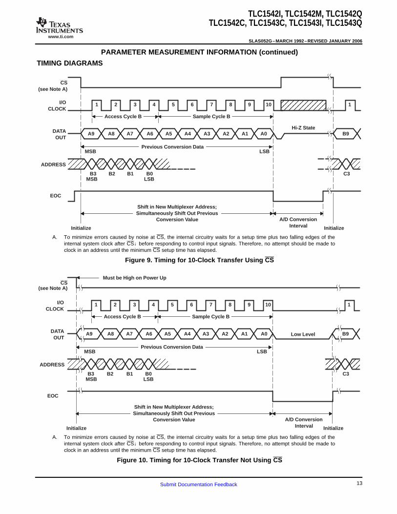
TIMINGMODES CS NO. OF 1/O CLOCK MSB AT DATA OUT (1)DIAGRAM
Mode 1 High between conversion cycles 10 CS falling edge Figure 9
Mode 2 Low continuously 10 EOC rising edge Figure 10Fast Modes
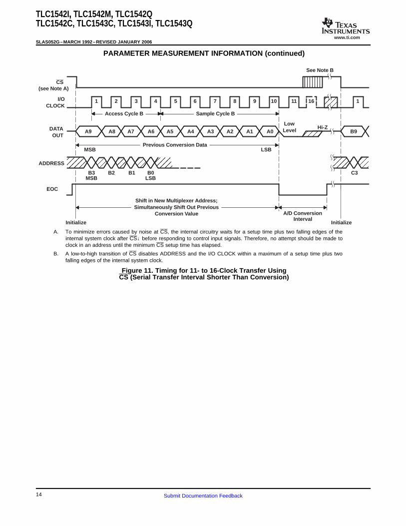
Mode 3 High between conversion cycles 11 TO 16 (2) CS falling edge Figure 11
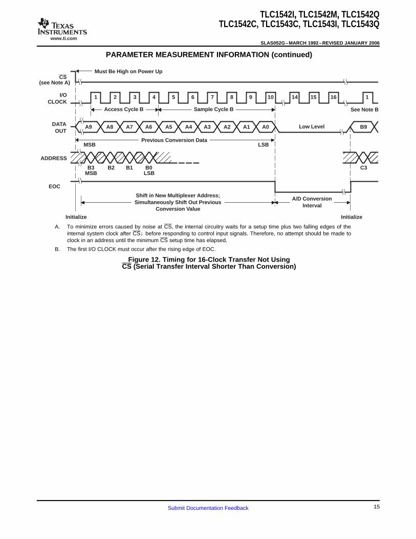
Mode 4 Low continuously 16 (2) EOC rising edge Figure 12
Mode 5 High between conversion cycles 11 to 16 (3) CS falling edge Figure 13Slow Modes
Mode 6 Low continuously 16 (3) 16th clock falling edge Figure 14
(1) These edges also initiate serial-interface communication.(2) No more than 16 clocks should be used.(3) No more than 16 clocks should be used.
The device is in a fast mode when the serial I/O CLOCK data transfer is completed before the conversion iscompleted. With a 10-clock serial transfer, the device can only run in a fast mode since a conversion does notbegin until the falling edge of the tenth I/O CLOCK.
In this mode, CS is inactive (high) between serial I/O CLOCK transfers and each transfer is ten clocks long. Thefalling edge of CS begins the sequence by removing DATA OUT from the high-impedance state. The rising edgeof CS ends the sequence by returning DATA OUT to the high-impedance state within the specified delay time.Also, the rising edge of CS disables the I/O CLOCK and ADDRESS terminals within a setup time plus two fallingedges of the internal system clock.
In this mode, CS is active (low) between serial I/O CLOCK transfers and each transfer is ten clocks long. Afterthe initial conversion cycle, CS is held active (low) for subsequent conversions; the rising edge of EOC thenbegins each sequence by removing DATA OUT from the low logic level, allowing the MSB of the previousconversion to appear immediately on this output.
TRANSFER
In this mode, CS is inactive (high) between serial I/O CLOCK transfers, and each transfer can be 11 to 16 clockslong. The falling edge of CS begins the sequence by removing DATA OUT from the high-impedance state. Therising edge of CS ends the sequence by returning DATA OUT to the high-impedance state within the specifieddelay time. Also, the rising edge of CS disables the I/O CLOCK and ADDRESS terminals within a setup timeplus two falling edges of the internal system clock.
4 Submit Documentation Feedback
www.ti.com
MODE 4: FAST MODE, CS ACTIVE (LOW) CONTINUOUSLY, 16-CLOCK TRANSFER
SLOW MODES
MODE 5: SLOW MODE, CS INACTIVE (HIGH) BETWEEN CONVERSION CYCLES, 11- to 16-CLOCK
MODE 6: SLOW MODE, CS ACTIVE (LOW) CONTINUOUSLY, 16-CLOCK TRANSFER
ADDRESS BITS
ANALOG INPUTS AND TEST MODES
TLC1542I,, TLC1542M,, TLC1542QTLC1542C, TLC1543C, TLC1543I, TLC1543Q
SLAS052G–MARCH 1992–REVISED JANUARY 2006
In this mode, CS is active (low) between serial I/O CLOCK transfers and each transfer must be exactly 16 clockslong. After the initial conversion cycle, CS is held active (low) for subsequent conversions; the rising edge ofEOC then begins each sequence by removing DATA OUT from the low logic level, allowing the MSB of theprevious conversion to appear immediately on this output.
In a slow mode, the conversion is completed before the serial I/O CLOCK data transfer is completed. A slowmode requires a minimum 11-clock transfer into I/O CLOCK, and the rising edge of the eleventh clock mustoccur before the conversion period is complete; otherwise, the device loses synchronization with the host-serialinterface and CS has to be toggled to initialize the system. The eleventh rising edge of the I/O CLOCK mustoccur within 9.5 µs after the tenth I/O clock falling edge.
TRANSFER
In this mode, CS is inactive (high) between serial I/O CLOCK transfers and each transfer can be 11 to 16 clockslong. The falling edge of CS begins the sequence by removing DATA OUT from the high-impedance state. Therising edge of CS ends the sequence by returning DATA OUT to the high-impedance state within the specifieddelay time. Also, the rising edge of CS disables the I/O CLOCK and ADDRESS terminals within a setup timeplus two falling edges of the internal system clock.
In this mode, CS is active (low) between serial I/O CLOCK transfers and each transfer must be exactly 16 clockslong. After the initial conversion cycle, CS is held active (low) for subsequent conversions. The falling edge ofthe sixteenth I/O CLOCK then begins each sequence by removing DATA OUT from the low state, allowing theMSB of the previous conversion to appear immediately at DATA OUT. The device is then ready for the next16-clock transfer initiated by the serial interface.
The 4-bit analog channel-select address for the next conversion cycle is presented to the ADDRESS terminal(MSB first) and is clocked into the address register on the first four leading edges of I/O CLOCK. This addressselects one of 14 inputs (11 analog inputs or three internal test inputs).
The 11 analog inputs and the three internal test inputs are selected by the 14-channel multiplexer according tothe input address as shown in Tables 2 and 3. The input multiplexer is a break-before-make type to reduceinput-to-input noise injection resulting from channel switching.
Sampling of the analog input starts on the falling edge of the fourth I/O CLOCK, and sampling continues for sixI/O CLOCK periods. The sample is held on the falling edge of the tenth I/O CLOCK. The three test inputs areapplied to the multiplexer, sampled, and converted in the same manner as the external analog inputs.
5Submit Documentation Feedback
www.ti.com
Vref+ − Vref−2
CONVERTER AND ANALOG INPUT
TLC1542I,, TLC1542M,, TLC1542QTLC1542C, TLC1543C, TLC1543I, TLC1543Q
SLAS052G–MARCH 1992–REVISED JANUARY 2006
Table 2. ANALOG-CHANNEL-SELECT ADDRESS
VALUE SHIFTED INTO ADDRESSINPUTANALOG INPUT SELECTED
BINARY HEX
A0 0000 0
A1 0001 1
A2 0010 2
A3 0011 3
A4 0100 4
A5 0101 5
A6 0110 6
A7 0111 7
A8 1000 8
A9 1001 9
A10 1010 A
Table 3. TEST-MODE-SELECT ADDRESS
VALUE SHIFTED INTOINTERNAL SELF-TEST ADDRESS INPUT OUTPUT RESULT (HEX) (2)
VOLTAGE SELECTED (1)
BINARY HEX
1011 B 200
Vref- 1100 C 000
Vref+ 1101 D 3FF
(1) Vref+ is the voltage applied to the REF+ input, and Vref- is the voltage applied to the REF- input.(2) The output results shown are the ideal values and vary with the reference stability and with internal
offsets.
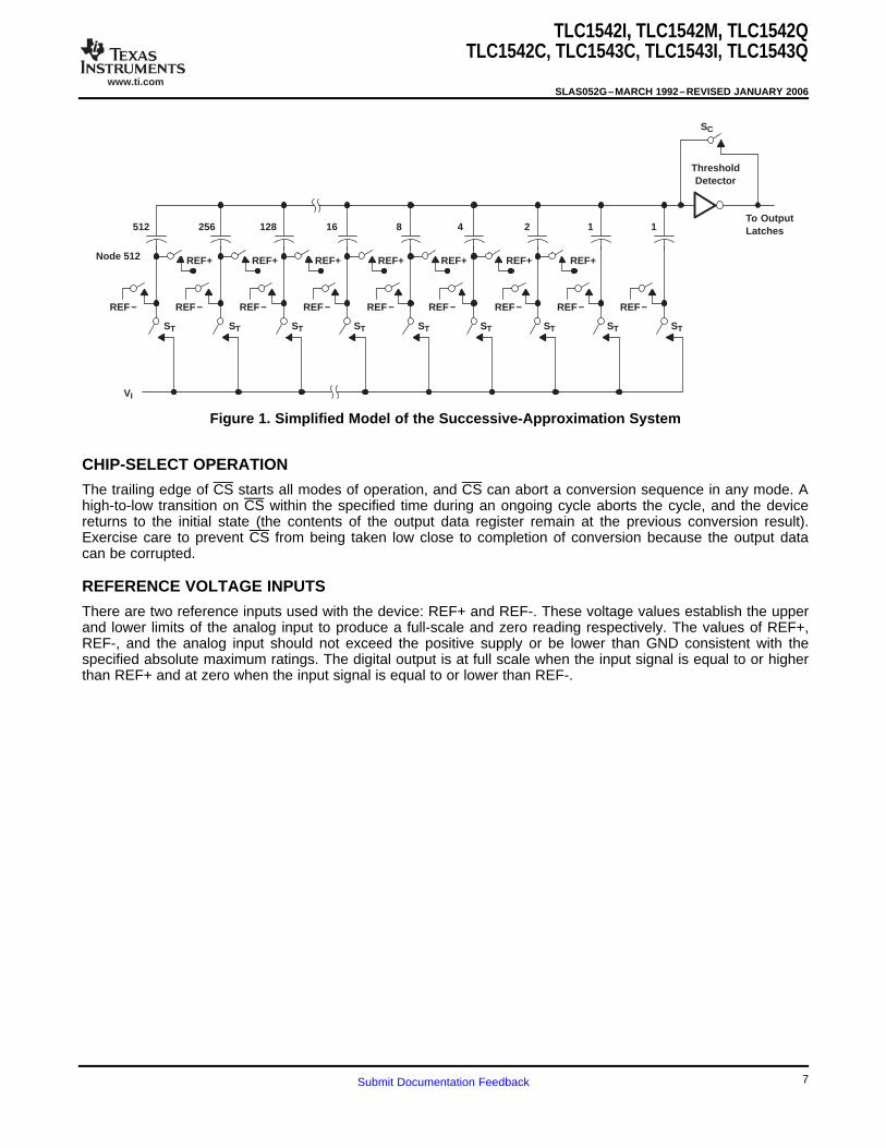
The CMOS threshold detector in the successive-approximation conversion system determines each bit byexamining the charge on a series of binary-weighted capacitors (see Figure 1). In the first phase of theconversion process, the analog input is sampled by closing the SC switch and all ST switches simultaneously.This action charges all the capacitors to the input voltage.
In the next phase of the conversion process, all ST and SC switches are opened and the threshold detectorbegins identifying bits by identifying the charge (voltage) on each capacitor relative to the reference (REF-)voltage. In the switching sequence, ten capacitors are examined separately until all ten bits are identified andthen the charge-convert sequence is repeated. In the first step of the conversion phase, the threshold detectorlooks at the first capacitor (weight = 512). Node 512 of this capacitor is switched to the REF+ voltage, and theequivalent nodes of all the other capacitors on the ladder are switched to REF-. If the voltage at the summingnode is greater than the trip point of the threshold detector (approximately one-half VCC), a 0 bit is placed in theoutput register and the 512-weight capacitor is switched to REF-. If the voltage at the summing node is less thanthe trip point of the threshold detector, a 1 bit is placed in the register and the 512-weight capacitor remainsconnected to REF+ through the remainder of the successive-approximation process. The process is repeated forthe 256-weight capacitor, the 128-weight capacitor, and so forth down the line until all bits are counted.
With each step of the successive-approximation process, the initial charge is redistributed among the capacitors.The conversion process relies on charge redistribution to count and weigh the bits from MSB to LSB.
6 Submit Documentation Feedback
www.ti.com
SC
ThresholdDetector
Node 512
REF−
REF+
ST
512
VI
To OutputLatches
REF+REF+ REF+ REF+
124816128256 1
REF+ REF+
REF− REF− REF− REF− REF− REF− REF− REF−
ST ST ST ST ST ST ST ST
CHIP-SELECT OPERATION
REFERENCE VOLTAGE INPUTS
TLC1542I,, TLC1542M,, TLC1542QTLC1542C, TLC1543C, TLC1543I, TLC1543Q
SLAS052G–MARCH 1992–REVISED JANUARY 2006
Figure 1. Simplified Model of the Successive-Approximation System
The trailing edge of CS starts all modes of operation, and CS can abort a conversion sequence in any mode. Ahigh-to-low transition on CS within the specified time during an ongoing cycle aborts the cycle, and the devicereturns to the initial state (the contents of the output data register remain at the previous conversion result).Exercise care to prevent CS from being taken low close to completion of conversion because the output datacan be corrupted.
There are two reference inputs used with the device: REF+ and REF-. These voltage values establish the upperand lower limits of the analog input to produce a full-scale and zero reading respectively. The values of REF+,REF-, and the analog input should not exceed the positive supply or be lower than GND consistent with thespecified absolute maximum ratings. The digital output is at full scale when the input signal is equal to or higherthan REF+ and at zero when the input signal is equal to or lower than REF-.
7Submit Documentation Feedback
www.ti.com
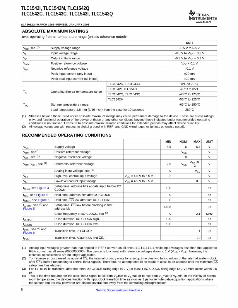
ABSOLUTE MAXIMUM RATINGS
RECOMMENDED OPERATING CONDITIONS
TLC1542I,, TLC1542M,, TLC1542QTLC1542C, TLC1543C, TLC1543I, TLC1543Q
SLAS052G–MARCH 1992–REVISED JANUARY 2006
over operating free-air temperature range (unless otherwise noted) (1)
UNIT
VCC, see (2) Supply voltage range -0.5 V to 6.5 V
VI Input voltage range -0.3 V to VCC + 0.3 V
VO Output voltage range -0.3 V to VCC + 0.3 V
Vref+ Positive reference voltage VCC + 0.1 V
Vref- Negative reference voltage -0.1 V
Peak input current (any input) ±20 mA
Peak total input current (all inputs) ±30 mA
TLC1542C, TLC1543C 0°C to 70°C
TLC1542I, TLC1543I -40°C to 85°CTA Operating free-air temperature range
TLC1542Q, TLC1543Q -40°C to 125°C
TLC1542M -55°C to 125°C
Tstg Storage temperature range, -65°C to 150°C
Lead temperature 1,6 mm (1/16 inch) from the case for 10 seconds 260°C
(1) Stresses beyond those listed under absolute maximum ratings may cause permanent damage to the device. These are stress ratingsonly, and functional operation of the device at these or any other conditions beyond those indicated under recommended operatingconditions is not implied. Exposure to absolute-maximum-rated conditions for extended periods may affect device reliability.
(2) All voltage values are with respect to digital ground with REF- and GND wired together (unless otherwise noted).
MIN NOM MAX UNIT
VCC Supply voltage 4.5 5 5.5 V
Vref+, see (1) Positive reference voltage VCC V
Vref-, see (1) Negative reference voltage 0 V
VCC+0.Vref+-Vref-, see (1) Differential reference voltage 2.5 VCC V2
Analog input voltage ,see (1) 0 VCC V
VIH High-level control input voltage VCC = 4.5 V to 5.5 V 2 V
VIL Low-level control input voltage VCC = 4.5 V to 5.5 V 0.8 V
Setup time, address bits at data input before I/Otsu(A), see Figure 4 100 nsCLOCK↑
th(A), see Figure 4 Hold time, address bits after I/O CLOCK↑ 0 ns
th(CS), see Figure 5 Hold time, CS low after last I/O CLOCK↓ 0 ns
tsu(CS), see (2) and Setup time, CS low before clocking in first 1.425 µsFigure 5 address bit
Clock frequency at I/O CLOCK, see (3) 0 2.1 MHz
twH(I/O) Pulse duration, I/O CLOCK high, 190 ns
twL(I/O) Pulse duration, I/O CLOCK low, 190 ns
tt(I/O), see (4) and Transition time, I/O CLOCK, 1 µsFigure 6
tt(CS) Transition time, ADDRESS and CS, 10 µs
(1) Analog input voltages greater than that applied to REF+ convert as all ones (1111111111), while input voltages less than that applied toREF- convert as all zeros (0000000000). The device is functional with reference voltages down to 1 V (Vref+ - Vref-); however, theelectrical specifications are no longer applicable.
(2) To minimize errors caused by noise at CS, the internal circuitry waits for a setup time plus two falling edges of the internal system clockafter CS↓ before responding to control input signals. Therefore, no attempt should be made to clock in an address until the minimum CSsetup time has elapsed.
(3) For 11- to 16-bit transfers, after the tenth I/O CLOCK falling edge (≤ 2 V) at least 1 I/O CLOCK rising edge (≥ 2 V) must occur within 9.5µs.
(4) This is the time required for the clock input signal to fall from VIHmin to VILmax or to rise from VILmax to VIHmin. In the vicinity of normalroom temperature, the devices function with input clock transition time as slow as 1 µs for remote data-acquisition applications wherethe sensor and the A/D converter are placed several feet away from the controlling microprocessor.
8 Submit Documentation Feedback
www.ti.com
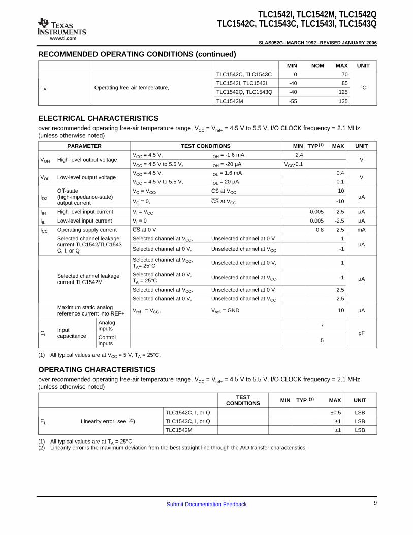
ELECTRICAL CHARACTERISTICS
OPERATING CHARACTERISTICS
TLC1542I,, TLC1542M,, TLC1542QTLC1542C, TLC1543C, TLC1543I, TLC1543Q
SLAS052G–MARCH 1992–REVISED JANUARY 2006
RECOMMENDED OPERATING CONDITIONS (continued)MIN NOM MAX UNIT
TLC1542C, TLC1543C 0 70
TLC1542I, TLC1543I -40 85TA Operating free-air temperature, °C
TLC1542Q, TLC1543Q -40 125
TLC1542M -55 125
over recommended operating free-air temperature range, VCC = Vref+ = 4.5 V to 5.5 V, I/O CLOCK frequency = 2.1 MHz(unless otherwise noted)
PARAMETER TEST CONDITIONS MIN TYP (1) MAX UNIT
VCC = 4.5 V, IOH = -1.6 mA 2.4VOH High-level output voltage V
VCC = 4.5 V to 5.5 V, IOH = -20 µA VCC-0.1
VCC = 4.5 V, IOL = 1.6 mA 0.4VOL Low-level output voltage V
VCC = 4.5 V to 5.5 V, IOL = 20 µA 0.1
Off-state VO = VCC, CS at VCC 10IOZ (high-impedance-state) µA
VO = 0, CS at VCC -10output current
IIH High-level input current VI = VCC 0.005 2.5 µA
IIL Low-level input current VI = 0 0.005 -2.5 µA
ICC Operating supply current CS at 0 V 0.8 2.5 mA
Selected channel leakage Selected channel at VCC, Unselected channel at 0 V 1current TLC1542/TLC1543 µA
Selected channel at 0 V, Unselected channel at VCC -1C, I, or Q
Selected channel at VCC, Unselected channel at 0 V, 1TA= 25°C
Selected channel at 0 V,Selected channel leakage Unselected channel at VCC, -1 µATA = 25°Ccurrent TLC1542MSelected channel at VCC, Unselected channel at 0 V 2.5
Selected channel at 0 V, Unselected channel at VCC -2.5
Maximum static analog Vref+ = VCC, Vref- = GND 10 µAreference current into REF+
Analog 7inputsInputCi pFcapacitance Control 5inputs
(1) All typical values are at VCC = 5 V, TA = 25°C.
over recommended operating free-air temperature range, VCC = Vref+ = 4.5 V to 5.5 V, I/O CLOCK frequency = 2.1 MHz(unless otherwise noted)
TEST MIN TYP (1) MAX UNITCONDITIONS
TLC1542C, I, or Q ±0.5 LSB
EL Linearity error, see (2)) TLC1543C, I, or Q ±1 LSB
TLC1542M ±1 LSB
(1) All typical values are at TA = 25°C.(2) Linearity error is the maximum deviation from the best straight line through the A/D transfer characteristics.
9Submit Documentation Feedback
www.ti.com
TLC1542I,, TLC1542M,, TLC1542QTLC1542C, TLC1543C, TLC1543I, TLC1543Q
SLAS052G–MARCH 1992–REVISED JANUARY 2006
OPERATING CHARACTERISTICS (continued)over recommended operating free-air temperature range, VCC = Vref+ = 4.5 V to 5.5 V, I/O CLOCK frequency = 2.1 MHz(unless otherwise noted)
TEST MIN TYP (1) MAX UNITCONDITIONS
TLC1542C, I, or Q See (4) ±1 LSB
EZS Zero-scale error, see (3) TLC1543C, I, or Q See (4) ±1 LSB
TLC1542M See (4) ±1 LSB
TLC1542C, I, or Q See (4) ±1 LSB
EFS Full-scale error, see (3) TLC1543C, I, or Q See (4) ±1 LSB
TLC1542M See (4) ±1 LSB
TLC1542C, I, or Q ±1 LSB
Total unadjusted error, see (5) TLC1543C, I, or Q ±1 LSB
TLC1542M ±1 LSB
ADDRESS = 1011 512
Self-test output code, see Table 3 and (6) ADDRESS = 1100 0
ADDRESS = 1101 1023
See timingtconv Conversion time 21 µsdiagrams
21See timing +10 I/Otc Total cycle time (access, sample, and conversion) µsdiagrams and (7) CLOCK
periods
See timing I/O CLOCKtacq Channel acquisition time (sample) 6diagrams and (7) periods
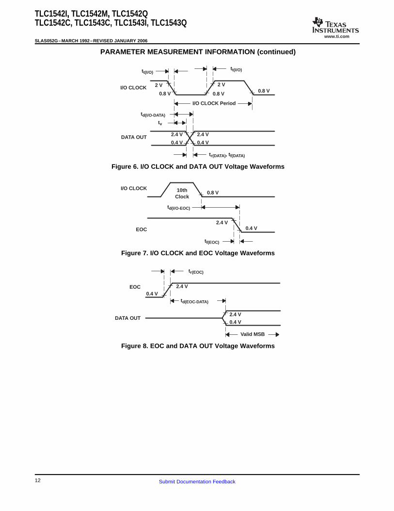
tv Valid time, DATA OUT remains valid after I/O CLOCK↓ See Figure 6 10 ns
td(I/O-DATA) Delay time, I/O CLOCK↓ to DATA OUT valid See Figure 6 240 ns
td(I/O-EOC) Delay time, tenth I/O CLOCK↓ to EOC↓ See Figure 7 70 240 ns
td(EOC-DATA) Delay time, EOC↑ to DATA OUT (MSB) See Figure 8 100 ns
tPZH, tPZL Enable time, CS↓ to DATA OUT (MSB driven) See Figure 3 1.3 µs
tPHZ, tPLZ Disable time, CS↑ to DATA OUT (high impedance) See Figure 3 150 ns
tr(EOC) Rise time, EOC See Figure 8 300 ns
tf(EOC) Fall time, EOC See Figure 7 300 ns
tr(DATA) Rise time, data bus See Figure 6 300 ns
tf(DATA) Fall time, data bus See Figure 6 300 ns
Delay time, tenth I/O CLOCK↓ to CS↓ to aborttd(I/O-CS) 9 µsconversion (see Note (8))
(3) Zero-scale error is the difference between 0000000000 and the converted output for zero input voltage; full-scale error is the differencebetween 1111111111 and the converted output for full-scale input voltage.
(4) Analog input voltages greater than that applied to REF+ convert as all ones (1111111111), while input voltages less than that applied toREF- convert as all zeros (0000000000). The device is functional with reference voltages down to 1 V (Vref+-Vref-); however, theelectrical specifications are no longer applicable.
(5) Total unadjusted error comprises linearity, zero-scale, and full-scale errors.(6) Both the input address and the output codes are expressed in positive logic.(7) I/O CLOCK period = 1/(I/O CLOCK frequency) (see Figure 6)(8) Any transitions of CS are recognized as valid only if the level is maintained for a setup time plus two falling edges of the internal clock
(1.425 µs) after the transition.
10 Submit Documentation Feedback
www.ti.com
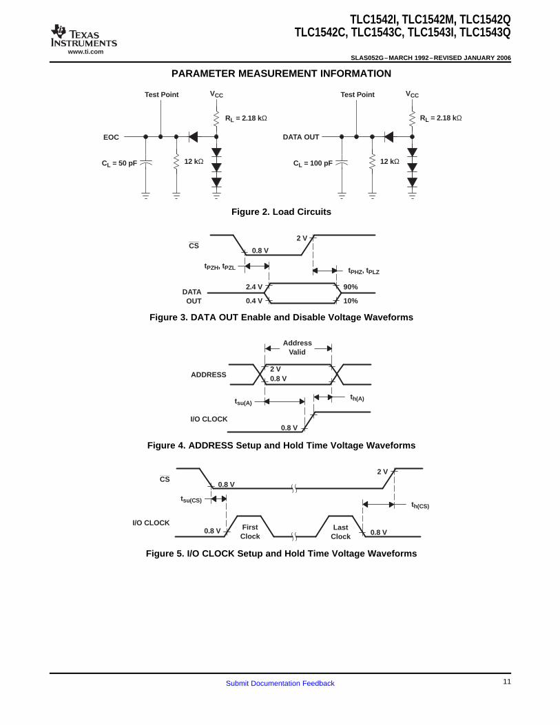
PARAMETER MEASUREMENT INFORMATION
EOC
CL = 50 pF 12 kΩ
DATA OUT
Test Point VCC
RL = 2.18 kΩ
CL = 100 pF 12 kΩ
Test Point VCC
RL = 2.18 kΩ
CS
DATAOUT
2.4 V
0.4 V
90%
10%
tPZH, tPZL tPHZ, tPLZ
0.8 V
2 V
ADDRESS
th(A)
0.8 V2 V
I/O CLOCK
AddressValid
tsu(A)
0.8 V
LastClock
CS0.8 V
2 V
0.8 V
tsu(CS)
0.8 VI/O CLOCK
th(CS)
FirstClock
TLC1542I,, TLC1542M,, TLC1542QTLC1542C, TLC1543C, TLC1543I, TLC1543Q
SLAS052G–MARCH 1992–REVISED JANUARY 2006
Figure 2. Load Circuits
Figure 3. DATA OUT Enable and Disable Voltage Waveforms
Figure 4. ADDRESS Setup and Hold Time Voltage Waveforms
Figure 5. I/O CLOCK Setup and Hold Time Voltage Waveforms
11Submit Documentation Feedback
www.ti.com
0.4 V
2.4 V
0.4 V
2.4 V
2 V0.8 V
I/O CLOCK
DATA OUT
tt(I/O)
0.8 V
2 V
tr(DATA) , tf(DATA)
td(I/O-DATA)
tv
tt(I/O)
0.8 V
I/O CLOCK Period
10thClock
0.8 V
2.4 V0.4 V
tf(EOC)
td(I/O-EOC)
I/O CLOCK
EOC
0.4 V
2.4 V
EOC
Valid MSB
DATA OUT
0.4 V2.4 V
tr(EOC)
td(EOC-DATA)
TLC1542I,, TLC1542M,, TLC1542QTLC1542C, TLC1543C, TLC1543I, TLC1543Q
SLAS052G–MARCH 1992–REVISED JANUARY 2006
PARAMETER MEASUREMENT INFORMATION (continued)
Figure 6. I/O CLOCK and DATA OUT Voltage Waveforms
Figure 7. I/O CLOCK and EOC Voltage Waveforms
Figure 8. EOC and DATA OUT Voltage Waveforms
12 Submit Documentation Feedback
www.ti.com
TIMING DIAGRAMS ÎÎÎÎÎÎÎÎÎÎÎÎÎÎÎÎÎÎÎÎÎÎÎÎÎÎÎÎÎÎÎÎÎÎÎÎÎÎÎÎÎÎÎÎÎÎÎÎÎÎÎÎÎÎÎÎÎÎÎÎÎÎÎÎÎÎÎÎ ÎÎÎÎÎÎÎÎÎÎÎÎÎÎÎÎAccess Cycle B
Shift in New Multiplexer Address;Simultaneously Shift Out Previous
Conversion V alue
Sample Cycle B
A/D ConversionInterval InitializeInitialize
MSB LSBPrevious Conversion Data
MSB LSBB3 B2 B1 B0 C3
B9A9 A8 A7 A6 A5 A4 A3 A2 A1 A0Hi-Z State
1 2 3 4 5 6 7 8 9 10 1I/OCLOCK
DATAOUT
ADDRESS
CS(see Note A)
EOC
ÎÎÎÎÎÎÎÎÎÎÎÎÎÎÎÎÎÎÎÎÎÎÎÎÎÎÎÎÎÎÎÎÎÎÎÎÎÎÎÎÎÎÎÎ ÎÎÎÎÎÎÎÎÎÎÎÎÎÎÎÎÎÎÎÎAccess Cycle B
Shift in New Multiplexer Address;Simultaneously Shift Out Previous
Conversion Value
Sample Cycle B
A/D ConversionIntervalInitialize
MSB LSBPrevious Conversion Data
MSB LSBB3 B2 B1 B0 C3
B9A9 A8 A7 A6 A5 A4 A3 A2 A1 A0 Low Level
1 2 3 4 5 6 7 8 9 10 1I/OCLOCK
DATAOUT
ADDRESS
CS
EOC
Initialize
(see Note A)
Must be High on Power Up
TLC1542I,, TLC1542M,, TLC1542QTLC1542C, TLC1543C, TLC1543I, TLC1543Q
SLAS052G–MARCH 1992–REVISED JANUARY 2006
PARAMETER MEASUREMENT INFORMATION (continued)
A. To minimize errors caused by noise at CS, the internal circuitry waits for a setup time plus two falling edges of theinternal system clock after CS↓ before responding to control input signals. Therefore, no attempt should be made toclock in an address until the minimum CS setup time has elapsed.
Figure 9. Timing for 10-Clock Transfer Using CS
A. To minimize errors caused by noise at CS, the internal circuitry waits for a setup time plus two falling edges of theinternal system clock after CS↓ before responding to control input signals. Therefore, no attempt should be made toclock in an address until the minimum CS setup time has elapsed.
Figure 10. Timing for 10-Clock Transfer Not Using CS
13Submit Documentation Feedback
www.ti.com
ÎÎÎÎÎÎÎÎÎÎÎÎÎÎÎÎÎÎÎÎÎÎÎÎÎÎÎÎÎÎÎÎÎÎÎÎÎÎÎÎÎÎÎÎÎÎÎÎ ÎÎÎÎÎÎÎÎÎÎÎÎÎÎÎÎÎÎÎÎAccess Cycle B
Shift in New Multiplexer Address;Simultaneously Shift Out Previous
Conversion V alue
Sample Cycle B
A/D ConversionInterval
Initialize
MSB LSBPrevious Conversion Data
MSB LSBB3 B2 B1 B0 C3
B9A9 A8 A7 A6 A5 A4 A3 A2 A1 A0
1 2 3 4 5 6 7 8 9 10 1I/OCLOCK
DATAOUT
ADDRESS
CS
EOC
Initialize
ÏÏÏÏÏÏÏÏÏÏÏÏÎÎÎÎÎÎÎÎÎÎÎÎÎÎÎÎÎÎÎÎÎLowLevel Hi-Z
See Note B
11 16
(see Note A)
TLC1542I,, TLC1542M,, TLC1542QTLC1542C, TLC1543C, TLC1543I, TLC1543Q
SLAS052G–MARCH 1992–REVISED JANUARY 2006
PARAMETER MEASUREMENT INFORMATION (continued)
A. To minimize errors caused by noise at CS, the internal circuitry waits for a setup time plus two falling edges of theinternal system clock after CS↓ before responding to control input signals. Therefore, no attempt should be made toclock in an address until the minimum CS setup time has elapsed.
B. A low-to-high transition of CS disables ADDRESS and the I/O CLOCK within a maximum of a setup time plus twofalling edges of the internal system clock.
Figure 11. Timing for 11- to 16-Clock Transfer UsingCS (Serial Transfer Interval Shorter Than Conversion)
14 Submit Documentation Feedback
www.ti.com
ÎÎÎÎÎÎÎÎÎÎÎÎÎÎÎÎÎÎÎÎÎÎÎÎÎÎÎÎÎÎÎÎ ÎÎÎÎÎÎÎÎÎÎÎÎÎÎÎÎÎÎÎÎAccess Cycle B
Shift in New Multiplexer Address;Simultaneously Shift Out Previous
Conversion Value
Sample Cycle B
A/D ConversionInterval
Initialize
MSB LSBPrevious Conversion Data
MSB LSBB3 B2 B1 B0 C3
B9A9 A8 A7 A6 A5 A4 A3 A2 A1 A0 Low Level
1 2 3 4 5 6 7 8 9 10 1I/OCLOCK
DATAOUT
ADDRESS
CS
EOC
Initialize
Must Be High on Power Up
14 15 16
See Note B
(see Note A) ÎÎÎÎÎÎÎÎÎÎÎÎTLC1542I,, TLC1542M,, TLC1542Q
TLC1542C, TLC1543C, TLC1543I, TLC1543Q
SLAS052G–MARCH 1992–REVISED JANUARY 2006
PARAMETER MEASUREMENT INFORMATION (continued)
A. To minimize errors caused by noise at CS, the internal circuitry waits for a setup time plus two falling edges of theinternal system clock after CS↓ before responding to control input signals. Therefore, no attempt should be made toclock in an address until the minimum CS setup time has elapsed.
B. The first I/O CLOCK must occur after the rising edge of EOC.
Figure 12. Timing for 16-Clock Transfer Not UsingCS (Serial Transfer Interval Shorter Than Conversion)
15Submit Documentation Feedback
www.ti.com
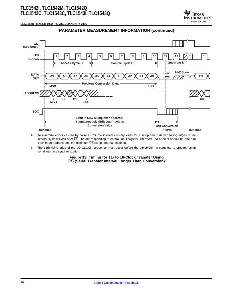
ÎÎÎÎÎÎÎÎÎÎÎÎÎÎÎÎÎÎÎÎÎÎÎÎÎÎÎÎÎÎÎÎÎÎÎÎÎÎÎÎÎÎÎÎ ÎÎÎÎÎÎÎÎÎÎÎÎÎÎÎÎAccess Cycle B
Shift in New Multiplexer Address;Simultaneously Shift Out Previous
Conversion V alue
Sample Cycle B
A/D ConversionIntervalInitialize
MSB LSBPrevious Conversion Data
MSB LSBB3 B2 B1 B0 C3
B9A9 A8 A7 A6 A5 A4 A3 A2 A1 A0
1 2 3 4 5 6 7 8 9 10 1I/OCLOCK
DATAOUT
ADDRESS
CS
EOC
Initialize
11
ÏÏÏÏÏÏÏÏÏÏÏÏÎÎÎÎÎÎÎÎÎÎÎÎÎÎÎÎÎHi-Z State
16
See Note BÏÏÏÏÏÏÏÏÏÏÏÏLowLevel
(see Note A)
TLC1542I,, TLC1542M,, TLC1542QTLC1542C, TLC1543C, TLC1543I, TLC1543Q
SLAS052G–MARCH 1992–REVISED JANUARY 2006
PARAMETER MEASUREMENT INFORMATION (continued)
A. To minimize errors caused by noise at CS, the internal circuitry waits for a setup time plus two falling edges of theinternal system clock after CS↓ before responding to control input signals. Therefore, no attempt should be made toclock in an address until the minimum CS setup time has elapsed.
B. The 11th rising edge of the I/O CLOCK sequence must occur before the conversion is complete to prevent losingserial interface synchronization.
Figure 13. Timing for 11- to 16-Clock Transfer UsingCS (Serial Transfer Interval Longer Than Conversion)
16 Submit Documentation Feedback
www.ti.com
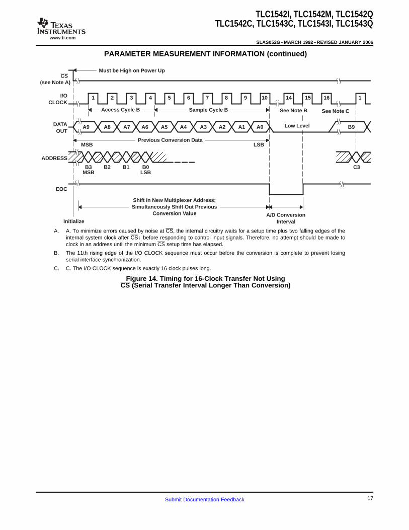
ÎÎÎÎÎÎÎÎÎÎÎÎÎÎÎÎÎÎÎÎÎÎÎÎÎÎÎÎÎÎÎÎÎÎÎÎÎÎÎÎÎÎÎÎ ÎÎÎÎÎÎÎÎÎÎÎÎÎÎÎÎÎÎÎÎShift in New Multiplexer Address;Simultaneously Shift Out Previous
Conversion Value
Sample Cycle B
A/D ConversionIntervalInitialize
MSB LSBPrevious Conversion Data
MSB LSBB3 B2 B1 B0 C3
B9A9 A8 A7 A6 A5 A4 A3 A2 A1 A0
1 2 3 4 5 6 7 8 9 10 1I/OCLOCK
DATAOUT
ADDRESS
CS
EOC
Must be High on Power Up
14 15 16
See Note CSee Note B
Low Level
Access Cycle B
(see Note A)
TLC1542I,, TLC1542M,, TLC1542QTLC1542C, TLC1543C, TLC1543I, TLC1543Q
SLAS052G–MARCH 1992–REVISED JANUARY 2006
PARAMETER MEASUREMENT INFORMATION (continued)
A. A. To minimize errors caused by noise at CS, the internal circuitry waits for a setup time plus two falling edges of theinternal system clock after CS↓ before responding to control input signals. Therefore, no attempt should be made toclock in an address until the minimum CS setup time has elapsed.
B. The 11th rising edge of the I/O CLOCK sequence must occur before the conversion is complete to prevent losingserial interface synchronization.
C. C. The I/O CLOCK sequence is exactly 16 clock pulses long.
Figure 14. Timing for 16-Clock Transfer Not UsingCS (Serial Transfer Interval Longer Than Conversion)
17Submit Documentation Feedback
www.ti.com
APPLICATION INFORMATION
1000000000
0111111111
0000000010
0000000001
0000000000
1111111110
0 0.0096 2.4528 2.4576 2.4624
Dig
ital O
utpu
t Cod
e 1000000001
1111111101
1111111111
4.9056 4.9104 4.9152
512
511
2
1
0
1022
Ste
p
513
1021
1023
0.00
24
VI − Analog Input V oltage − V
VZT =VZS + 1/2 LSB
VZS
See Notes A and B
4.90
800.0048
VFT = VFS − 1/2 LSB
VFS
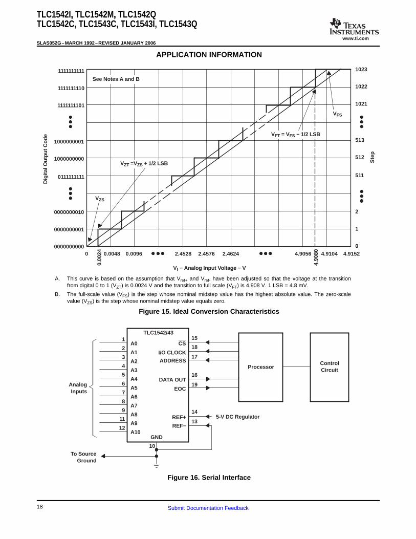
ProcessorControlCircuit
AnalogInputs
A0
A1
A2
A3
A4
A5
A6
A7
A8
A9
A10
I/O CLOCK
CS
ADDRESS
DATA OUT
EOC
REF+
REF−
GND
TLC1542/43
To SourceGround
5-V DC Regulator
1
2
3
4
5
6
7
8
9
11
12
15
18
17
16
19
14
13
10
TLC1542I,, TLC1542M,, TLC1542QTLC1542C, TLC1543C, TLC1543I, TLC1543Q
SLAS052G–MARCH 1992–REVISED JANUARY 2006
A. This curve is based on the assumption that Vref+ and Vref- have been adjusted so that the voltage at the transitionfrom digital 0 to 1 (VZT) is 0.0024 V and the transition to full scale (VFT) is 4.908 V. 1 LSB = 4.8 mV.
B. The full-scale value (VFS) is the step whose nominal midstep value has the highest absolute value. The zero-scalevalue (VZS) is the step whose nominal midstep value equals zero.
Figure 15. Ideal Conversion Characteristics
Figure 16. Serial Interface
18 Submit Documentation Feedback
www.ti.com
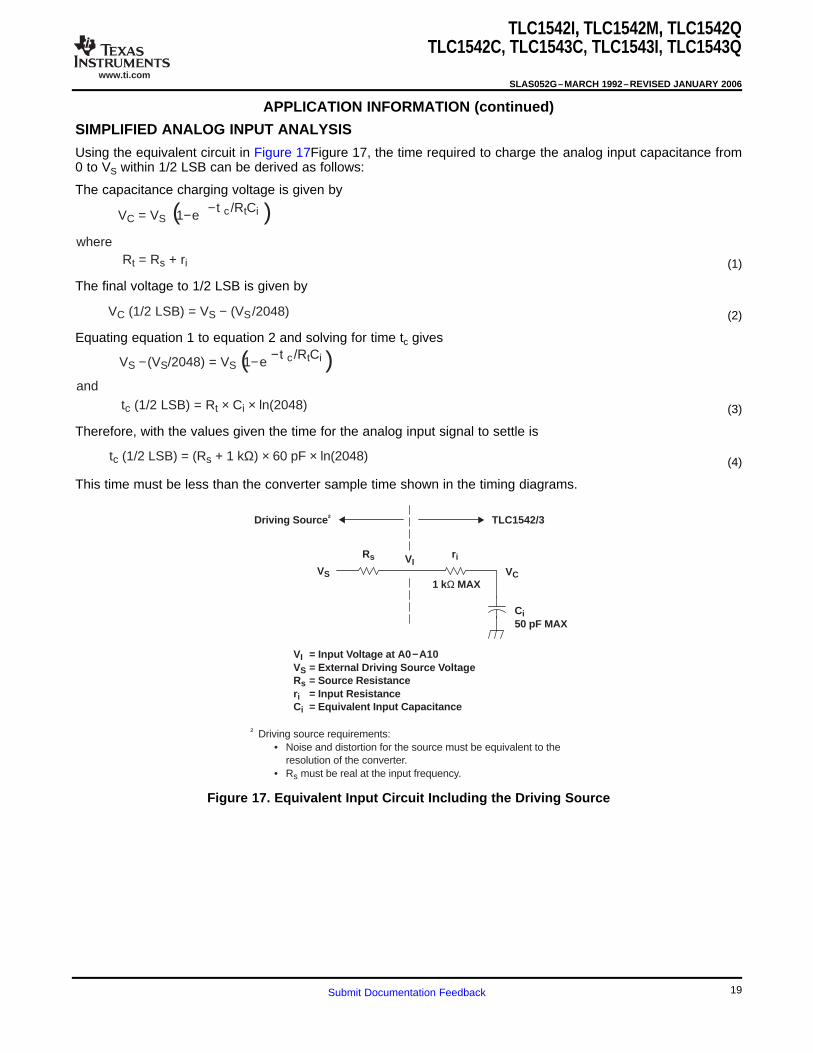
SIMPLIFIED ANALOG INPUT ANALYSIS
VC = VS 1−e −t c /RtCi( )where
Rt = Rs + ri (1)
VC (1/2 LSB) = VS − (VS /2048) (2)
VS −(VS/2048) = VS 1−e( )−t c /RtCi
andtc (1/2 LSB) = Rt × Ci × ln(2048)
(3)
tc (1/2 LSB) = (Rs + 1 kΩ) × 60 pF × ln(2048) (4)
Rs r i
VS VC1 kΩ MAX
Driving Source † TLC1542/3
Ci50 pF MAX
VI
VI = Input V oltage at A0 −A10VS = External Driving Source V oltageRs = Source Resistancer i = Input ResistanceCi = Equivalent Input Capacitance
† Driving source requirements:• Noise and distortion for the source must be equivalent to the
resolution of the converter.• Rs must be real at the input frequency.
TLC1542I,, TLC1542M,, TLC1542QTLC1542C, TLC1543C, TLC1543I, TLC1543Q
SLAS052G–MARCH 1992–REVISED JANUARY 2006
APPLICATION INFORMATION (continued)
Using the equivalent circuit in Figure 17Figure 17, the time required to charge the analog input capacitance from0 to VS within 1/2 LSB can be derived as follows:
The capacitance charging voltage is given by
The final voltage to 1/2 LSB is given by
Equating equation 1 to equation 2 and solving for time tc gives
Therefore, with the values given the time for the analog input signal to settle is
This time must be less than the converter sample time shown in the timing diagrams.
Figure 17. Equivalent Input Circuit Including the Driving Source
19Submit Documentation Feedback
PACKAGE OPTION ADDENDUM
www.ti.com 17-Mar-2017
Addendum-Page 1
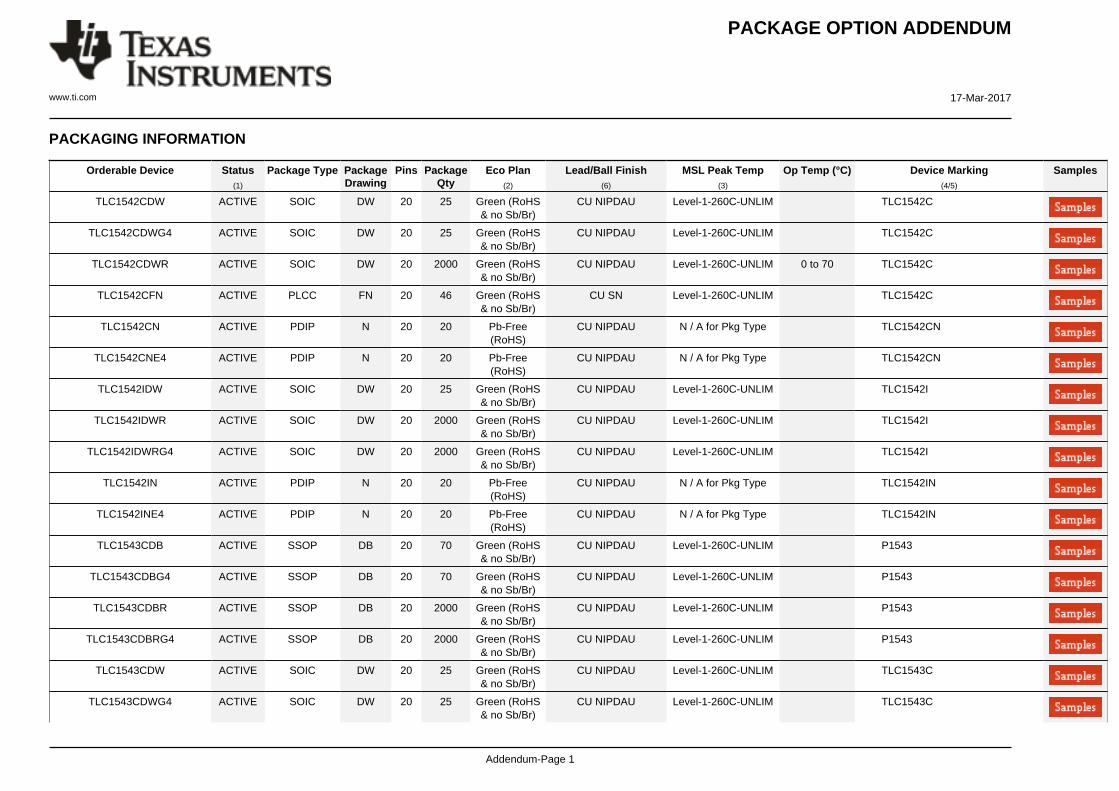
PACKAGING INFORMATION
Orderable Device Status(1)
Package Type PackageDrawing
Pins PackageQty
Eco Plan(2)
Lead/Ball Finish(6)
MSL Peak Temp(3)
Op Temp (°C) Device Marking(4/5)
Samples
TLC1542CDW ACTIVE SOIC DW 20 25 Green (RoHS& no Sb/Br)
CU NIPDAU Level-1-260C-UNLIM TLC1542C
TLC1542CDWG4 ACTIVE SOIC DW 20 25 Green (RoHS& no Sb/Br)
CU NIPDAU Level-1-260C-UNLIM TLC1542C
TLC1542CDWR ACTIVE SOIC DW 20 2000 Green (RoHS& no Sb/Br)
CU NIPDAU Level-1-260C-UNLIM 0 to 70 TLC1542C
TLC1542CFN ACTIVE PLCC FN 20 46 Green (RoHS& no Sb/Br)
CU SN Level-1-260C-UNLIM TLC1542C
TLC1542CN ACTIVE PDIP N 20 20 Pb-Free(RoHS)
CU NIPDAU N / A for Pkg Type TLC1542CN
TLC1542CNE4 ACTIVE PDIP N 20 20 Pb-Free(RoHS)
CU NIPDAU N / A for Pkg Type TLC1542CN
TLC1542IDW ACTIVE SOIC DW 20 25 Green (RoHS& no Sb/Br)
CU NIPDAU Level-1-260C-UNLIM TLC1542I
TLC1542IDWR ACTIVE SOIC DW 20 2000 Green (RoHS& no Sb/Br)
CU NIPDAU Level-1-260C-UNLIM TLC1542I
TLC1542IDWRG4 ACTIVE SOIC DW 20 2000 Green (RoHS& no Sb/Br)
CU NIPDAU Level-1-260C-UNLIM TLC1542I
TLC1542IN ACTIVE PDIP N 20 20 Pb-Free(RoHS)
CU NIPDAU N / A for Pkg Type TLC1542IN
TLC1542INE4 ACTIVE PDIP N 20 20 Pb-Free(RoHS)
CU NIPDAU N / A for Pkg Type TLC1542IN
TLC1543CDB ACTIVE SSOP DB 20 70 Green (RoHS& no Sb/Br)
CU NIPDAU Level-1-260C-UNLIM P1543
TLC1543CDBG4 ACTIVE SSOP DB 20 70 Green (RoHS& no Sb/Br)
CU NIPDAU Level-1-260C-UNLIM P1543
TLC1543CDBR ACTIVE SSOP DB 20 2000 Green (RoHS& no Sb/Br)
CU NIPDAU Level-1-260C-UNLIM P1543
TLC1543CDBRG4 ACTIVE SSOP DB 20 2000 Green (RoHS& no Sb/Br)
CU NIPDAU Level-1-260C-UNLIM P1543
TLC1543CDW ACTIVE SOIC DW 20 25 Green (RoHS& no Sb/Br)
CU NIPDAU Level-1-260C-UNLIM TLC1543C
TLC1543CDWG4 ACTIVE SOIC DW 20 25 Green (RoHS& no Sb/Br)
CU NIPDAU Level-1-260C-UNLIM TLC1543C
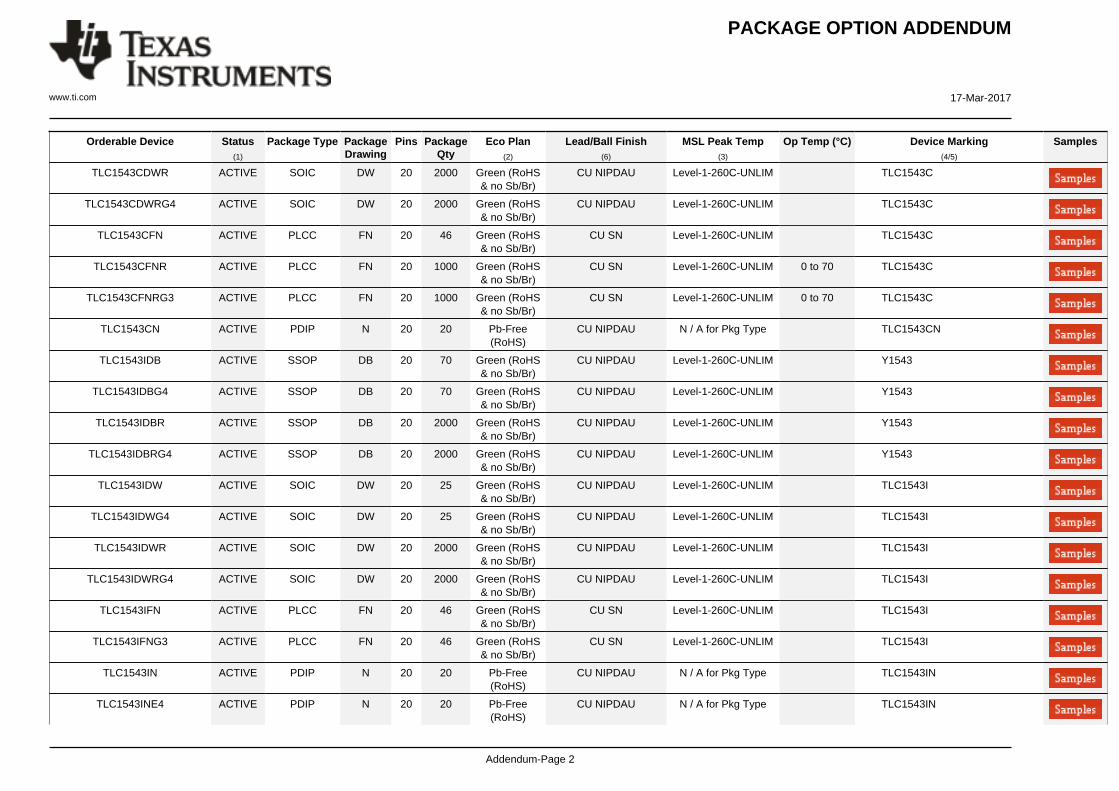
PACKAGE OPTION ADDENDUM
www.ti.com 17-Mar-2017
Addendum-Page 2
Orderable Device Status(1)
Package Type PackageDrawing
Pins PackageQty
Eco Plan(2)
Lead/Ball Finish(6)
MSL Peak Temp(3)
Op Temp (°C) Device Marking(4/5)
Samples
TLC1543CDWR ACTIVE SOIC DW 20 2000 Green (RoHS& no Sb/Br)
CU NIPDAU Level-1-260C-UNLIM TLC1543C
TLC1543CDWRG4 ACTIVE SOIC DW 20 2000 Green (RoHS& no Sb/Br)
CU NIPDAU Level-1-260C-UNLIM TLC1543C
TLC1543CFN ACTIVE PLCC FN 20 46 Green (RoHS& no Sb/Br)
CU SN Level-1-260C-UNLIM TLC1543C
TLC1543CFNR ACTIVE PLCC FN 20 1000 Green (RoHS& no Sb/Br)
CU SN Level-1-260C-UNLIM 0 to 70 TLC1543C
TLC1543CFNRG3 ACTIVE PLCC FN 20 1000 Green (RoHS& no Sb/Br)
CU SN Level-1-260C-UNLIM 0 to 70 TLC1543C
TLC1543CN ACTIVE PDIP N 20 20 Pb-Free(RoHS)
CU NIPDAU N / A for Pkg Type TLC1543CN
TLC1543IDB ACTIVE SSOP DB 20 70 Green (RoHS& no Sb/Br)
CU NIPDAU Level-1-260C-UNLIM Y1543
TLC1543IDBG4 ACTIVE SSOP DB 20 70 Green (RoHS& no Sb/Br)
CU NIPDAU Level-1-260C-UNLIM Y1543
TLC1543IDBR ACTIVE SSOP DB 20 2000 Green (RoHS& no Sb/Br)
CU NIPDAU Level-1-260C-UNLIM Y1543
TLC1543IDBRG4 ACTIVE SSOP DB 20 2000 Green (RoHS& no Sb/Br)
CU NIPDAU Level-1-260C-UNLIM Y1543
TLC1543IDW ACTIVE SOIC DW 20 25 Green (RoHS& no Sb/Br)
CU NIPDAU Level-1-260C-UNLIM TLC1543I
TLC1543IDWG4 ACTIVE SOIC DW 20 25 Green (RoHS& no Sb/Br)
CU NIPDAU Level-1-260C-UNLIM TLC1543I
TLC1543IDWR ACTIVE SOIC DW 20 2000 Green (RoHS& no Sb/Br)
CU NIPDAU Level-1-260C-UNLIM TLC1543I
TLC1543IDWRG4 ACTIVE SOIC DW 20 2000 Green (RoHS& no Sb/Br)
CU NIPDAU Level-1-260C-UNLIM TLC1543I
TLC1543IFN ACTIVE PLCC FN 20 46 Green (RoHS& no Sb/Br)
CU SN Level-1-260C-UNLIM TLC1543I
TLC1543IFNG3 ACTIVE PLCC FN 20 46 Green (RoHS& no Sb/Br)
CU SN Level-1-260C-UNLIM TLC1543I
TLC1543IN ACTIVE PDIP N 20 20 Pb-Free(RoHS)
CU NIPDAU N / A for Pkg Type TLC1543IN
TLC1543INE4 ACTIVE PDIP N 20 20 Pb-Free(RoHS)
CU NIPDAU N / A for Pkg Type TLC1543IN
PACKAGE OPTION ADDENDUM
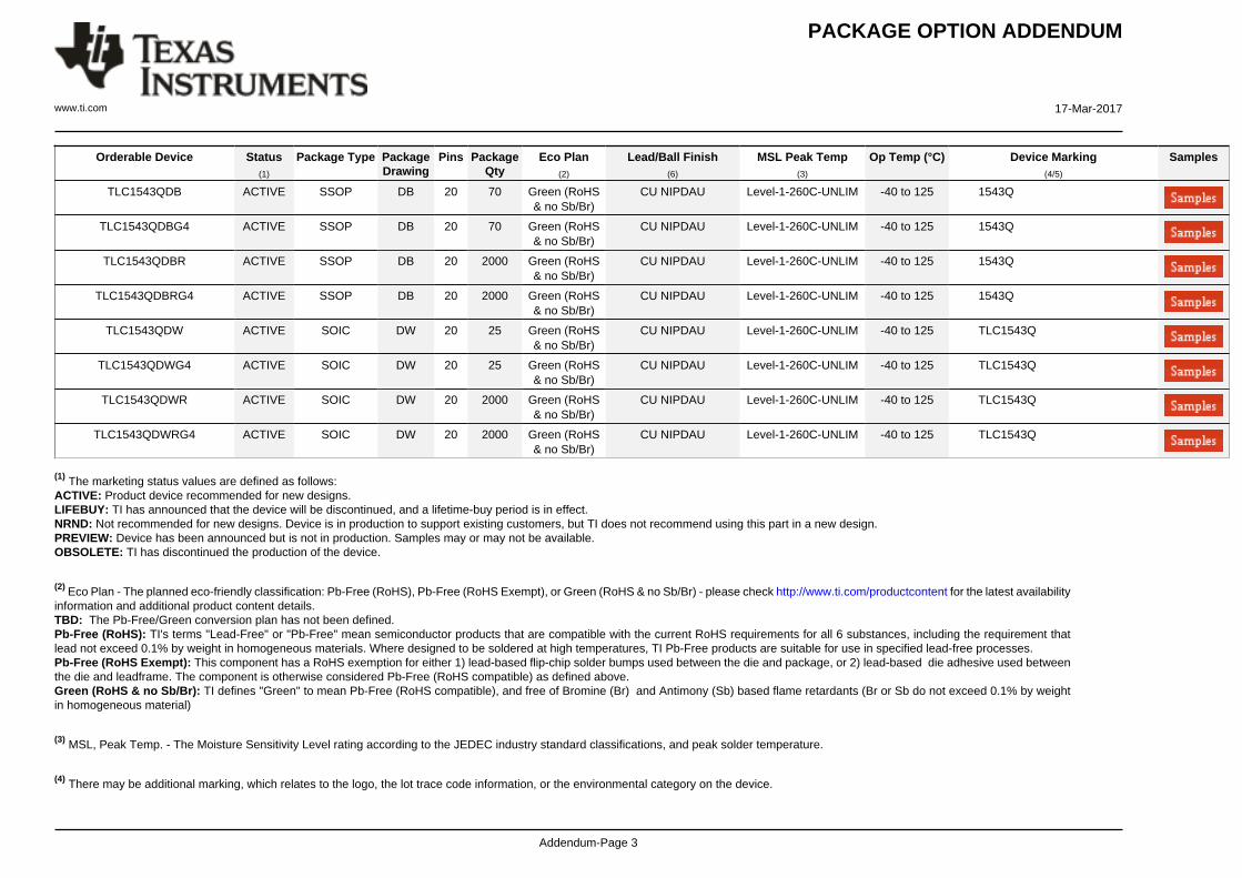
www.ti.com 17-Mar-2017
Addendum-Page 3
Orderable Device Status(1)
Package Type PackageDrawing
Pins PackageQty
Eco Plan(2)
Lead/Ball Finish(6)
MSL Peak Temp(3)
Op Temp (°C) Device Marking(4/5)
Samples
TLC1543QDB ACTIVE SSOP DB 20 70 Green (RoHS& no Sb/Br)
CU NIPDAU Level-1-260C-UNLIM -40 to 125 1543Q
TLC1543QDBG4 ACTIVE SSOP DB 20 70 Green (RoHS& no Sb/Br)
CU NIPDAU Level-1-260C-UNLIM -40 to 125 1543Q
TLC1543QDBR ACTIVE SSOP DB 20 2000 Green (RoHS& no Sb/Br)
CU NIPDAU Level-1-260C-UNLIM -40 to 125 1543Q
TLC1543QDBRG4 ACTIVE SSOP DB 20 2000 Green (RoHS& no Sb/Br)
CU NIPDAU Level-1-260C-UNLIM -40 to 125 1543Q
TLC1543QDW ACTIVE SOIC DW 20 25 Green (RoHS& no Sb/Br)
CU NIPDAU Level-1-260C-UNLIM -40 to 125 TLC1543Q
TLC1543QDWG4 ACTIVE SOIC DW 20 25 Green (RoHS& no Sb/Br)
CU NIPDAU Level-1-260C-UNLIM -40 to 125 TLC1543Q
TLC1543QDWR ACTIVE SOIC DW 20 2000 Green (RoHS& no Sb/Br)
CU NIPDAU Level-1-260C-UNLIM -40 to 125 TLC1543Q
TLC1543QDWRG4 ACTIVE SOIC DW 20 2000 Green (RoHS& no Sb/Br)
CU NIPDAU Level-1-260C-UNLIM -40 to 125 TLC1543Q
(1) The marketing status values are defined as follows:ACTIVE: Product device recommended for new designs.LIFEBUY: TI has announced that the device will be discontinued, and a lifetime-buy period is in effect.NRND: Not recommended for new designs. Device is in production to support existing customers, but TI does not recommend using this part in a new design.PREVIEW: Device has been announced but is not in production. Samples may or may not be available.OBSOLETE: TI has discontinued the production of the device.
(2) Eco Plan - The planned eco-friendly classification: Pb-Free (RoHS), Pb-Free (RoHS Exempt), or Green (RoHS & no Sb/Br) - please check http://www.ti.com/productcontent for the latest availabilityinformation and additional product content details.TBD: The Pb-Free/Green conversion plan has not been defined.Pb-Free (RoHS): TI's terms "Lead-Free" or "Pb-Free" mean semiconductor products that are compatible with the current RoHS requirements for all 6 substances, including the requirement thatlead not exceed 0.1% by weight in homogeneous materials. Where designed to be soldered at high temperatures, TI Pb-Free products are suitable for use in specified lead-free processes.Pb-Free (RoHS Exempt): This component has a RoHS exemption for either 1) lead-based flip-chip solder bumps used between the die and package, or 2) lead-based die adhesive used betweenthe die and leadframe. The component is otherwise considered Pb-Free (RoHS compatible) as defined above.Green (RoHS & no Sb/Br): TI defines "Green" to mean Pb-Free (RoHS compatible), and free of Bromine (Br) and Antimony (Sb) based flame retardants (Br or Sb do not exceed 0.1% by weightin homogeneous material)
(3) MSL, Peak Temp. - The Moisture Sensitivity Level rating according to the JEDEC industry standard classifications, and peak solder temperature.
(4) There may be additional marking, which relates to the logo, the lot trace code information, or the environmental category on the device.
PACKAGE OPTION ADDENDUM
www.ti.com 17-Mar-2017
Addendum-Page 4
(5) Multiple Device Markings will be inside parentheses. Only one Device Marking contained in parentheses and separated by a "~" will appear on a device. If a line is indented then it is a continuationof the previous line and the two combined represent the entire Device Marking for that device.
(6) Lead/Ball Finish - Orderable Devices may have multiple material finish options. Finish options are separated by a vertical ruled line. Lead/Ball Finish values may wrap to two lines if the finishvalue exceeds the maximum column width.
Important Information and Disclaimer:The information provided on this page represents TI's knowledge and belief as of the date that it is provided. TI bases its knowledge and belief on informationprovided by third parties, and makes no representation or warranty as to the accuracy of such information. Efforts are underway to better integrate information from third parties. TI has taken andcontinues to take reasonable steps to provide representative and accurate information but may not have conducted destructive testing or chemical analysis on incoming materials and chemicals.TI and TI suppliers consider certain information to be proprietary, and thus CAS numbers and other limited information may not be available for release.
In no event shall TI's liability arising out of such information exceed the total purchase price of the TI part(s) at issue in this document sold by TI to Customer on an annual basis.
OTHER QUALIFIED VERSIONS OF TLC1543 :
• Enhanced Product: TLC1543-EP
NOTE: Qualified Version Definitions:
• Enhanced Product - Supports Defense, Aerospace and Medical Applications
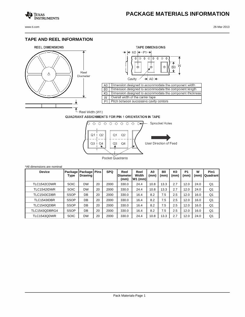
TAPE AND REEL INFORMATION
*All dimensions are nominal
Device PackageType
PackageDrawing
Pins SPQ ReelDiameter
(mm)
ReelWidth
W1 (mm)
A0(mm)
B0(mm)
K0(mm)
P1(mm)
W(mm)
Pin1Quadrant
TLC1542CDWR SOIC DW 20 2000 330.0 24.4 10.8 13.3 2.7 12.0 24.0 Q1
TLC1542IDWR SOIC DW 20 2000 330.0 24.4 10.8 13.3 2.7 12.0 24.0 Q1
TLC1543CDBR SSOP DB 20 2000 330.0 16.4 8.2 7.5 2.5 12.0 16.0 Q1
TLC1543IDBR SSOP DB 20 2000 330.0 16.4 8.2 7.5 2.5 12.0 16.0 Q1
TLC1543QDBR SSOP DB 20 2000 330.0 16.4 8.2 7.5 2.5 12.0 16.0 Q1
TLC1543QDBRG4 SSOP DB 20 2000 330.0 16.4 8.2 7.5 2.5 12.0 16.0 Q1
TLC1543QDWR SOIC DW 20 2000 330.0 24.4 10.8 13.3 2.7 12.0 24.0 Q1
PACKAGE MATERIALS INFORMATION
www.ti.com 26-Mar-2013
Pack Materials-Page 1
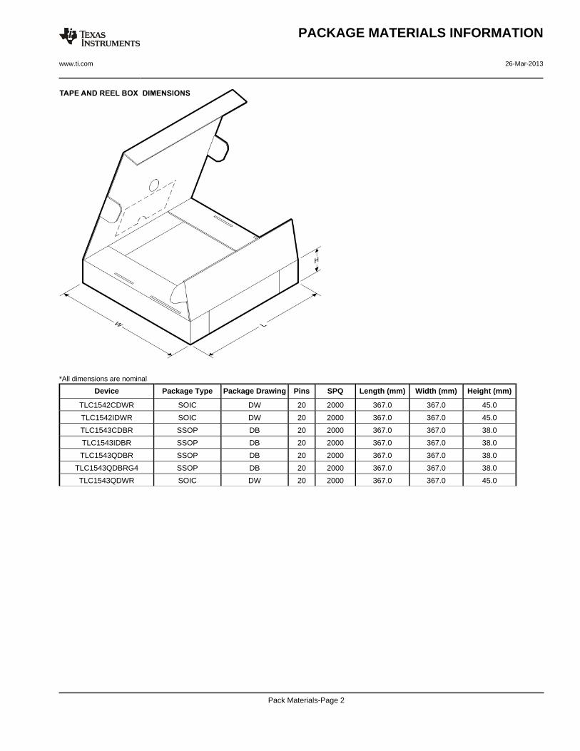
*All dimensions are nominal
Device Package Type Package Drawing Pins SPQ Length (mm) Width (mm) Height (mm)
TLC1542CDWR SOIC DW 20 2000 367.0 367.0 45.0
TLC1542IDWR SOIC DW 20 2000 367.0 367.0 45.0
TLC1543CDBR SSOP DB 20 2000 367.0 367.0 38.0
TLC1543IDBR SSOP DB 20 2000 367.0 367.0 38.0
TLC1543QDBR SSOP DB 20 2000 367.0 367.0 38.0
TLC1543QDBRG4 SSOP DB 20 2000 367.0 367.0 38.0
TLC1543QDWR SOIC DW 20 2000 367.0 367.0 45.0
PACKAGE MATERIALS INFORMATION
www.ti.com 26-Mar-2013
Pack Materials-Page 2
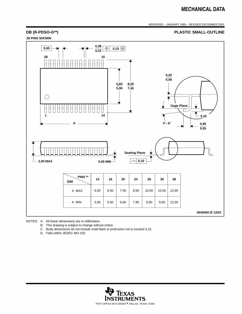
MECHANICAL DATA
MSSO002E – JANUARY 1995 – REVISED DECEMBER 2001
POST OFFICE BOX 655303 • DALLAS, TEXAS 75265
DB (R-PDSO-G**) PLASTIC SMALL-OUTLINE
4040065 /E 12/01
28 PINS SHOWN
Gage Plane
8,207,40
0,550,95
0,25
38
12,90
12,30
28
10,50
24
8,50
Seating Plane
9,907,90
30
10,50
9,90
0,38
5,605,00
15
0,22
14
A
28
1
2016
6,506,50
14
0,05 MIN
5,905,90
DIM
A MAX
A MIN
PINS **
2,00 MAX
6,90
7,50
0,65 M0,15
0°–8°
0,10
0,090,25
NOTES: A. All linear dimensions are in millimeters.B. This drawing is subject to change without notice.C. Body dimensions do not include mold flash or protrusion not to exceed 0,15.D. Falls within JEDEC MO-150
www.ti.com
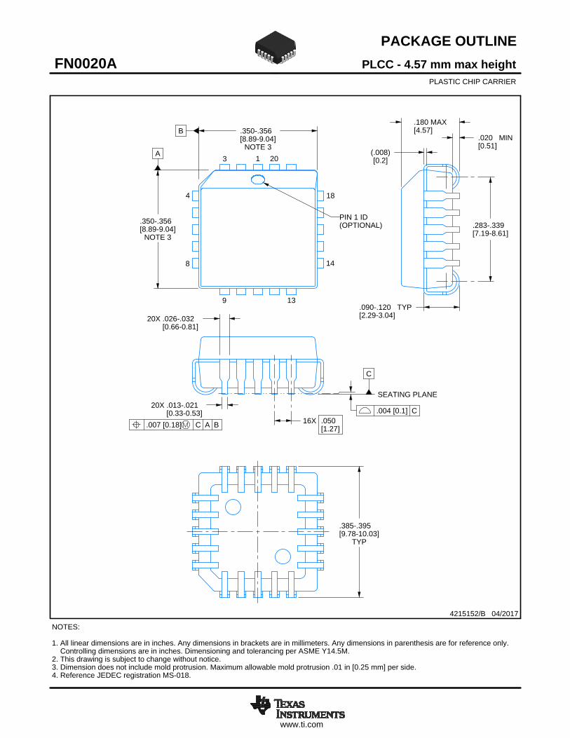
PACKAGE OUTLINE
C
20X -.021.013-0.530.33[ ]
20X -.032.026-0.810.66[ ]
TYP
-.395.385-10.039.78[ ]
16X .050[1.27]
-.339.283-8.617.19[ ]
(.008)[0.2]
TYP-.120.090-3.042.29[ ]
.180 MAX[4.57]
.020 MIN[0.51]
B
NOTE 3
-.356.350-9.048.89[ ]
A
NOTE 3
-.356.350-9.048.89[ ]
4215152/B 04/2017
4215152/B 04/2017
PLCC - 4.57 mm max heightFN0020APLASTIC CHIP CARRIER
NOTES: 1. All linear dimensions are in inches. Any dimensions in brackets are in millimeters. Any dimensions in parenthesis are for reference only. Controlling dimensions are in inches. Dimensioning and tolerancing per ASME Y14.5M. 2. This drawing is subject to change without notice.3. Dimension does not include mold protrusion. Maximum allowable mold protrusion .01 in [0.25 mm] per side.4. Reference JEDEC registration MS-018.
PIN 1 ID(OPTIONAL)
1 203
9 13
14
184
8
.004 [0.1] C
.007 [0.18] C A B
SEATING PLANE
SCALE 1.300
www.ti.com
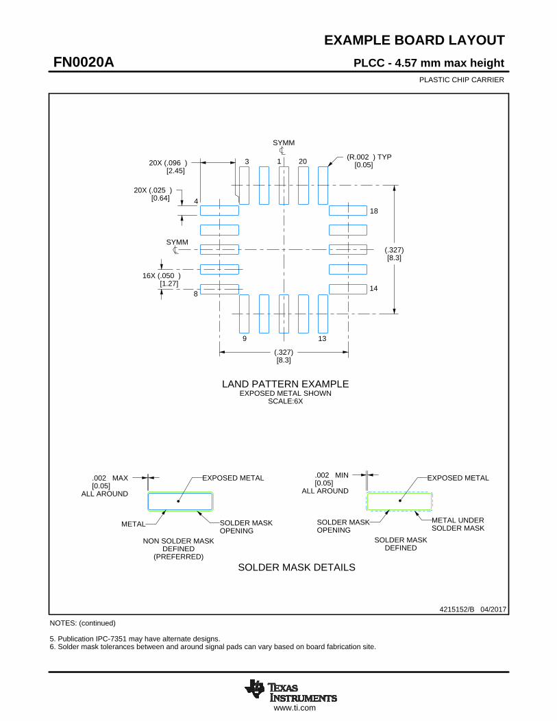
EXAMPLE BOARD LAYOUT
.002 MAX[0.05]
ALL AROUND
.002 MIN[0.05]
ALL AROUND
20X (.096 )[2.45]
20X (.025 )[0.64]
16X (.050 )[1.27]
(.327)[8.3]
(.327)[8.3]
(R.002 ) TYP[0.05]
4215152/B 04/2017
4215152/B 04/2017
PLCC - 4.57 mm max heightFN0020APLASTIC CHIP CARRIER
NOTES: (continued) 5. Publication IPC-7351 may have alternate designs.6. Solder mask tolerances between and around signal pads can vary based on board fabrication site.
LAND PATTERN EXAMPLEEXPOSED METAL SHOWN
SCALE:6X
SYMM
SYMM
1 203
9 13
14
184
8
METAL SOLDER MASKOPENING
NON SOLDER MASKDEFINED
(PREFERRED)SOLDER MASK DETAILS
EXPOSED METAL
SOLDER MASKOPENING
METAL UNDERSOLDER MASK
SOLDER MASKDEFINED
EXPOSED METAL
www.ti.com
EXAMPLE STENCIL DESIGN
20X (.025 )[0.64]
20X (.096 )[2.45]
(.327)[8.3]
(.327)[8.3]
16X (.050 )[1.27]
(R.002 ) TYP[0.05]
PLCC - 4.57 mm max heightFN0020APLASTIC CHIP CARRIER
4215152/B 04/2017
PLCC - 4.57 mm max heightFN0020APLASTIC CHIP CARRIER
NOTES: (continued) 7. Laser cutting apertures with trapezoidal walls and rounded corners may offer better paste release. IPC-7525 may have alternate design recommendations.8. Board assembly site may have different recommendations for stencil design.
SOLDER PASTE EXAMPLEBASED ON 0.125 mm THICK STENCIL
SCALE:6X
SYMM
SYMM
1 203
9 13
14
184
8
www.ti.com
PACKAGE OUTLINE
C
TYP10.639.97
2.65 MAX
18X 1.27
20X 0.510.31
2X11.43
TYP0.330.10
0 - 80.30.1
0.25GAGE PLANE
1.270.40
A
NOTE 3
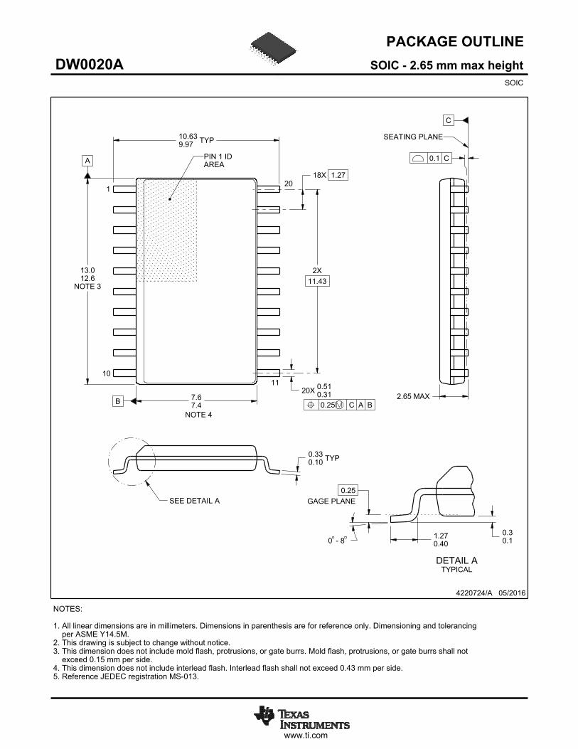
13.012.6
B 7.67.4
4220724/A 05/2016
SOIC - 2.65 mm max heightDW0020ASOIC
NOTES: 1. All linear dimensions are in millimeters. Dimensions in parenthesis are for reference only. Dimensioning and tolerancing per ASME Y14.5M. 2. This drawing is subject to change without notice. 3. This dimension does not include mold flash, protrusions, or gate burrs. Mold flash, protrusions, or gate burrs shall not exceed 0.15 mm per side. 4. This dimension does not include interlead flash. Interlead flash shall not exceed 0.43 mm per side.5. Reference JEDEC registration MS-013.
120
0.25 C A B
1110
PIN 1 IDAREA
NOTE 4
SEATING PLANE
0.1 C
SEE DETAIL A
DETAIL ATYPICAL
SCALE 1.200
www.ti.com
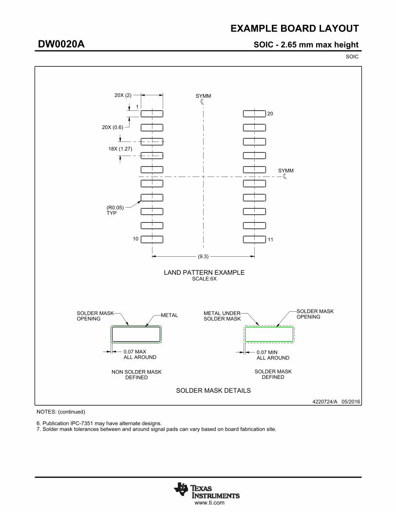
EXAMPLE BOARD LAYOUT
(9.3)
0.07 MAXALL AROUND
0.07 MINALL AROUND
20X (2)
20X (0.6)
18X (1.27)
(R )TYP
0.05
4220724/A 05/2016
SOIC - 2.65 mm max heightDW0020ASOIC
SYMM
SYMM
LAND PATTERN EXAMPLESCALE:6X
1
10 11
20
NOTES: (continued) 6. Publication IPC-7351 may have alternate designs. 7. Solder mask tolerances between and around signal pads can vary based on board fabrication site.
METALSOLDER MASKOPENING
NON SOLDER MASKDEFINED
SOLDER MASK DETAILS
SOLDER MASKOPENING
METAL UNDERSOLDER MASK
SOLDER MASKDEFINED
www.ti.com
EXAMPLE STENCIL DESIGN
(9.3)
18X (1.27)
20X (0.6)
20X (2)
4220724/A 05/2016
SOIC - 2.65 mm max heightDW0020ASOIC
NOTES: (continued) 8. Laser cutting apertures with trapezoidal walls and rounded corners may offer better paste release. IPC-7525 may have alternate design recommendations. 9. Board assembly site may have different recommendations for stencil design.
SYMM
SYMM
1
10 11
20
SOLDER PASTE EXAMPLEBASED ON 0.125 mm THICK STENCIL
SCALE:6X
IMPORTANT NOTICE
Texas Instruments Incorporated (TI) reserves the right to make corrections, enhancements, improvements and other changes to itssemiconductor products and services per JESD46, latest issue, and to discontinue any product or service per JESD48, latest issue. Buyersshould obtain the latest relevant information before placing orders and should verify that such information is current and complete.TI’s published terms of sale for semiconductor products (http://www.ti.com/sc/docs/stdterms.htm) apply to the sale of packaged integratedcircuit products that TI has qualified and released to market. Additional terms may apply to the use or sale of other types of TI products andservices.Reproduction of significant portions of TI information in TI data sheets is permissible only if reproduction is without alteration and isaccompanied by all associated warranties, conditions, limitations, and notices. TI is not responsible or liable for such reproduceddocumentation. Information of third parties may be subject to additional restrictions. Resale of TI products or services with statementsdifferent from or beyond the parameters stated by TI for that product or service voids all express and any implied warranties for theassociated TI product or service and is an unfair and deceptive business practice. TI is not responsible or liable for any such statements.Buyers and others who are developing systems that incorporate TI products (collectively, “Designers”) understand and agree that Designersremain responsible for using their independent analysis, evaluation and judgment in designing their applications and that Designers havefull and exclusive responsibility to assure the safety of Designers' applications and compliance of their applications (and of all TI productsused in or for Designers’ applications) with all applicable regulations, laws and other applicable requirements. Designer represents that, withrespect to their applications, Designer has all the necessary expertise to create and implement safeguards that (1) anticipate dangerousconsequences of failures, (2) monitor failures and their consequences, and (3) lessen the likelihood of failures that might cause harm andtake appropriate actions. Designer agrees that prior to using or distributing any applications that include TI products, Designer willthoroughly test such applications and the functionality of such TI products as used in such applications.TI’s provision of technical, application or other design advice, quality characterization, reliability data or other services or information,including, but not limited to, reference designs and materials relating to evaluation modules, (collectively, “TI Resources”) are intended toassist designers who are developing applications that incorporate TI products; by downloading, accessing or using TI Resources in anyway, Designer (individually or, if Designer is acting on behalf of a company, Designer’s company) agrees to use any particular TI Resourcesolely for this purpose and subject to the terms of this Notice.TI’s provision of TI Resources does not expand or otherwise alter TI’s applicable published warranties or warranty disclaimers for TIproducts, and no additional obligations or liabilities arise from TI providing such TI Resources. TI reserves the right to make corrections,enhancements, improvements and other changes to its TI Resources. TI has not conducted any testing other than that specificallydescribed in the published documentation for a particular TI Resource.Designer is authorized to use, copy and modify any individual TI Resource only in connection with the development of applications thatinclude the TI product(s) identified in such TI Resource. NO OTHER LICENSE, EXPRESS OR IMPLIED, BY ESTOPPEL OR OTHERWISETO ANY OTHER TI INTELLECTUAL PROPERTY RIGHT, AND NO LICENSE TO ANY TECHNOLOGY OR INTELLECTUAL PROPERTYRIGHT OF TI OR ANY THIRD PARTY IS GRANTED HEREIN, including but not limited to any patent right, copyright, mask work right, orother intellectual property right relating to any combination, machine, or process in which TI products or services are used. Informationregarding or referencing third-party products or services does not constitute a license to use such products or services, or a warranty orendorsement thereof. Use of TI Resources may require a license from a third party under the patents or other intellectual property of thethird party, or a license from TI under the patents or other intellectual property of TI.TI RESOURCES ARE PROVIDED “AS IS” AND WITH ALL FAULTS. TI DISCLAIMS ALL OTHER WARRANTIES ORREPRESENTATIONS, EXPRESS OR IMPLIED, REGARDING RESOURCES OR USE THEREOF, INCLUDING BUT NOT LIMITED TOACCURACY OR COMPLETENESS, TITLE, ANY EPIDEMIC FAILURE WARRANTY AND ANY IMPLIED WARRANTIES OFMERCHANTABILITY, FITNESS FOR A PARTICULAR PURPOSE, AND NON-INFRINGEMENT OF ANY THIRD PARTY INTELLECTUALPROPERTY RIGHTS. TI SHALL NOT BE LIABLE FOR AND SHALL NOT DEFEND OR INDEMNIFY DESIGNER AGAINST ANY CLAIM,INCLUDING BUT NOT LIMITED TO ANY INFRINGEMENT CLAIM THAT RELATES TO OR IS BASED ON ANY COMBINATION OFPRODUCTS EVEN IF DESCRIBED IN TI RESOURCES OR OTHERWISE. IN NO EVENT SHALL TI BE LIABLE FOR ANY ACTUAL,DIRECT, SPECIAL, COLLATERAL, INDIRECT, PUNITIVE, INCIDENTAL, CONSEQUENTIAL OR EXEMPLARY DAMAGES INCONNECTION WITH OR ARISING OUT OF TI RESOURCES OR USE THEREOF, AND REGARDLESS OF WHETHER TI HAS BEENADVISED OF THE POSSIBILITY OF SUCH DAMAGES.Unless TI has explicitly designated an individual product as meeting the requirements of a particular industry standard (e.g., ISO/TS 16949and ISO 26262), TI is not responsible for any failure to meet such industry standard requirements.Where TI specifically promotes products as facilitating functional safety or as compliant with industry functional safety standards, suchproducts are intended to help enable customers to design and create their own applications that meet applicable functional safety standardsand requirements. Using products in an application does not by itself establish any safety features in the application. Designers mustensure compliance with safety-related requirements and standards applicable to their applications. Designer may not use any TI products inlife-critical medical equipment unless authorized officers of the parties have executed a special contract specifically governing such use.Life-critical medical equipment is medical equipment where failure of such equipment would cause serious bodily injury or death (e.g., lifesupport, pacemakers, defibrillators, heart pumps, neurostimulators, and implantables). Such equipment includes, without limitation, allmedical devices identified by the U.S. Food and Drug Administration as Class III devices and equivalent classifications outside the U.S.TI may expressly designate certain products as completing a particular qualification (e.g., Q100, Military Grade, or Enhanced Product).Designers agree that it has the necessary expertise to select the product with the appropriate qualification designation for their applicationsand that proper product selection is at Designers’ own risk. Designers are solely responsible for compliance with all legal and regulatoryrequirements in connection with such selection.Designer will fully indemnify TI and its representatives against any damages, costs, losses, and/or liabilities arising out of Designer’s non-compliance with the terms and provisions of this Notice.
Mailing Address: Texas Instruments, Post Office Box 655303, Dallas, Texas 75265Copyright © 2017, Texas Instruments Incorporated
Related Documents