Single material TiO 2 double layers antireflection coating with photocatalytic property prepared by magnetron sputtering technique Zhaoyong Wang a, b , Ning Yao a, * , Xing Hu a a School of Physical Engineering and Laboratory of Material Physics, Zhengzhou University, Zhengzhou 450052, People's Republic of China b School of Mathematics and Physics, Henan Urban Construction University, Pingdingshan 467036, People's Republic of China article info Article history: Received 24 March 2014 Received in revised form 12 May 2014 Accepted 13 May 2014 Available online 23 May 2014 Keywords: Antireflection Photocatalysis EFMS technique abstract Single material TiO 2 was used to fabricate the double layers antireflection coating with photocatalytic property. TiO 2 layers with low and high refractive indices were prepared by the direct reactive magnetron sputtering technique and energy filtrating magnetron sputtering technique, respectively. The structure, surface morphology and optical property were tested by X-ray diffraction, field emission scanning electron microscope and spectroscopic ellipsometer. The photocatalytic property of the coating was evaluated by UVevis spectrophotometer. Results suggested that the coating had both antireflective and photocatalytic performances. The refractive indices of the top and bottom TiO 2 layers were 2.10 and 2.47 (at 600 nm), respectively. The average and max transmissivities were obtained of 88.4% and 98.9% in the wavelength range of 400e800 nm and the degradation rate on Rhodamine B was obtained of 0.0034 min 1 . © 2014 Elsevier Ltd. All rights reserved. 1. Introduction TiO 2 has been studied comprehensively because it is non-toxic, convenient to be obtained and easy to be doped by other materials. It has many excellent performances such as high energy gap, high refractive index, high electric inductivity and good chemical stability [1e3]. There are three kinds of TiO 2 including anatase, rutile and brookite [4], while the anatase and rutile TiO 2 are more widely studied and utilized for their better optical and structural properties. Anatase TiO 2 is commonly used as the photocatalytic materials for the high band gap. Also some researchers reported that the hybrid of anatase and rutile TiO 2 had better photocatalytic performance [5]. Since the discovery of photo stimulated water splitting on the TiO 2 electrodes in 1972 [9], the application of TiO 2 in the photocatalytic technology and method have been investigated [6e8]. However, TiO 2 coating with high transmissivity should also be provided in cir- cumstances such as the application in architectural glass and glass cover for solar cells. Therefore double functional coating with both of self-cleaning and antireflective properties is required. Anatase TiO 2 was not usually used as the surface layer for the large scattering losing due to the high refractive index (n ¼ 2.52) [10]. Some re- searchers have managed to fabricate the double functional coating [11e 16]. The antireflective and self-cleaning properties were realized by the low refractive index material and anatase TiO 2 . But two dis- advantages exist in the fabricating process. The first one is that lattice distortion for the different material will be induced during the annealing. And the second one is that the surface modification pro- cess is complicated. TiO 2 film can be prepared by several methods such as chemical vapor deposition (CVD), dealloying and anodic oxidation, Sol-Gel, radio fraction magnetron sputtering (RFMS) and direct current reactive magnetron sputtering (DMS) [17e21]. Compared with other methods, DMS technique was used to prepare TiO 2 films in our experiment for its special advantages that the deposition parameters are stable, easy to control and high quality film with uniform distributions can be deposited in fast speed. Double layers antireflection coating is commonly selected over single layer because two maximum can be achieved in the trans- mission spectrum. Furthermore the optical performance of the coating is less sensitive to the variations of the refractive index and layer thickness [22]. In this paper, single material double layers coating was fabri- cated by the well-matched individual TiO 2 layers with low and high refractive indices. Anatase TiO 2 with low refractive was fabricated by the DMS technique. TiO 2 with high refractive index was pre- pared by the energy filtrated magnetron sputtering (EFMS) tech- nique. Both the double functional properties of antireflection and photocatalysis were investigated. * Corresponding author. Tel.: þ86 371 67767832. E-mail address: [email protected] (N. Yao). Contents lists available at ScienceDirect Vacuum journal homepage: www.elsevier.com/locate/vacuum http://dx.doi.org/10.1016/j.vacuum.2014.05.009 0042-207X/© 2014 Elsevier Ltd. All rights reserved. Vacuum 108 (2014) 20e26

1-s2.0-S0042207X14001687-main
Dec 28, 2015
TiO2
Welcome message from author
This document is posted to help you gain knowledge. Please leave a comment to let me know what you think about it! Share it to your friends and learn new things together.
Transcript
lable at ScienceDirect
Vacuum 108 (2014) 20e26
Contents lists avai
Vacuum
journal homepage: www.elsevier .com/locate/vacuum
Single material TiO2 double layers antireflection coating withphotocatalytic property prepared by magnetron sputtering technique
Zhaoyong Wang a, b, Ning Yao a, *, Xing Hu a
a School of Physical Engineering and Laboratory of Material Physics, Zhengzhou University, Zhengzhou 450052, People's Republic of Chinab School of Mathematics and Physics, Henan Urban Construction University, Pingdingshan 467036, People's Republic of China
a r t i c l e i n f o
Article history:Received 24 March 2014Received in revised form12 May 2014Accepted 13 May 2014Available online 23 May 2014
Keywords:AntireflectionPhotocatalysisEFMS technique
* Corresponding author. Tel.: þ86 371 67767832.E-mail address: [email protected] (N. Yao).
http://dx.doi.org/10.1016/j.vacuum.2014.05.0090042-207X/© 2014 Elsevier Ltd. All rights reserved.
a b s t r a c t
Single material TiO2 was used to fabricate the double layers antireflection coating with photocatalyticproperty. TiO2 layers with low and high refractive indices were prepared by the direct reactive magnetronsputtering technique and energy filtrating magnetron sputtering technique, respectively. The structure,surfacemorphology and optical property were tested by X-ray diffraction, field emission scanning electronmicroscope and spectroscopic ellipsometer. The photocatalytic property of the coating was evaluated byUVevis spectrophotometer. Results suggested that the coating had both antireflective and photocatalyticperformances. The refractive indices of the top and bottom TiO2 layers were 2.10 and 2.47 (at 600 nm),respectively. The average and max transmissivities were obtained of 88.4% and 98.9% in the wavelengthrange of 400e800 nm and the degradation rate on Rhodamine B was obtained of 0.0034 min�1.
© 2014 Elsevier Ltd. All rights reserved.
1. Introduction
TiO2 has been studied comprehensively because it is non-toxic,convenient to be obtained and easy to be doped by other materials.It has many excellent performances such as high energy gap, highrefractive index, high electric inductivity and good chemical stability[1e3]. There are three kinds of TiO2 including anatase, rutile andbrookite [4], while the anatase and rutile TiO2 are more widelystudied and utilized for their better optical and structural properties.Anatase TiO2 is commonly used as the photocatalytic materials forthe high band gap. Also some researchers reported that the hybrid ofanatase and rutile TiO2 had better photocatalytic performance [5].Since the discovery of photo stimulated water splitting on the TiO2electrodes in 1972 [9], the application of TiO2 in the photocatalytictechnologyandmethodhavebeen investigated [6e8].However, TiO2coating with high transmissivity should also be provided in cir-cumstances such as the application in architectural glass and glasscover for solar cells. Therefore double functional coatingwith both ofself-cleaning and antireflective properties is required. Anatase TiO2was not usually used as the surface layer for the large scatteringlosing due to the high refractive index (n ¼ 2.52) [10]. Some re-searchers have managed to fabricate the double functional coating
[11e16]. The antireflective and self-cleaningpropertieswere realizedby the low refractive index material and anatase TiO2. But two dis-advantages exist in the fabricating process. Thefirst one is that latticedistortion for the different material will be induced during theannealing. And the second one is that the surface modification pro-cess is complicated. TiO2 film can be prepared by several methodssuch as chemical vapor deposition (CVD), dealloying and anodicoxidation, Sol-Gel, radio fraction magnetron sputtering (RFMS) anddirect current reactive magnetron sputtering (DMS) [17e21].Compared with other methods, DMS technique was used to prepareTiO2 films in our experiment for its special advantages that thedeposition parameters are stable, easy to control and high qualityfilmwith uniform distributions can be deposited in fast speed.
Double layers antireflection coating is commonly selected oversingle layer because two maximum can be achieved in the trans-mission spectrum. Furthermore the optical performance of thecoating is less sensitive to the variations of the refractive index andlayer thickness [22].
In this paper, single material double layers coating was fabri-cated by thewell-matched individual TiO2 layers with low and highrefractive indices. Anatase TiO2 with low refractive was fabricatedby the DMS technique. TiO2 with high refractive index was pre-pared by the energy filtrated magnetron sputtering (EFMS) tech-nique. Both the double functional properties of antireflection andphotocatalysis were investigated.

Fig. 2. Structure of single material TiO2 double layers antireflective coating.
Z. Wang et al. / Vacuum 108 (2014) 20e26 21
2. Experiments
2.1. Material preparation
The glass substrates were primarily cleaned before deposition.Sequentially they were soaked in the KMnO4 solution (40 g/l) for4 h, and then were ultrasonic cleaned in proper order with thedetergent solution, de-ionized water, acetone, de-ionized water,isopropyl alcohol and de-ionized water. Finally the substrates weredried in the oven.
Home made CS-300 DMS system was used to fabricate theTiO2 films on the substrates. Ti target (180 � 60 � 6 mm3, purity99.99%) and the substrate with 70 mm-distance between themwere set as the cathode and anode. The base pressure of below5.0 � 10�4 Pa was realized by the mechanical pump and molec-ular pump. As the substrates were heated to the given temper-ature, high-purity gas Ar (purity 99.999%) was introduced intothe chamber. Ar plasma was generated by the electric fieldapplied between the target and substrate. After the surface of thetarget was purified by the bombardment of Arþ for 5 min, reac-tive gas of O2 (purity 99.5%) was introduced in to deposit TiO2
film.In order to prepare films with better performances, EFMS
technique was designed on the base of the DMS technique [23].
Y ¼ CB¼ ng cos dL cos dH � nLng sin dL sin dH
�nH þ iðnL sin dL cos dH þ nH cos dL sin dHÞ
cos dL cos dH � nH sin dL sin dH�nL þ i
�ng sin dL cos dH
�nH þ ng cos dL sin dH
�nL (2)
The schematic diagram is illustrated in Fig. 1. The stainless metalfiltrating electrode in 0.1 mm thickness with square grid wasconnected with the anode (ground) in front of the substrate.
2.2. Preparation of double layers coating
The structure of the coating is illustrated in Fig. 2. TiO2 filmswith high and low refractive indices are marked as TiO2eH andTiO2-L. TiO2eH layer was first deposited by the EFMS technique andthen TiO2-L layer was prepared by the DMS technique on it.
Based on thematrix theory [24], the characteristic matrix for theconstruction of the film-substrate is given by Eq. (1).
Fig. 1. Schematic diagram of the EFMS technique.
�BC
�¼�
cos dL i=nL sin dLinL sin dL cos dL
��cos dH i=nH sin dH
inH sin dH cos dH
��1ng
�(1)
where n0, nL and nH represent the refractive indices of the air, lowrefractive index and high refractive index of the TiO2 films,respectively. d is the phase thickness and can be described byd ¼ (2p/l)nd for the normal incidence. Y given by Eq. (2) representsthe admittance of the film-substrate assembly.
For the normal incidence and equal phase thickness layers(nHdH ¼ nLdL ¼ l0/4), the reflectance (R) at the wavelength l0 turnsinto Eq. (3).
R ¼�n0 � Yn0 þ Y
�2
¼ n0 � n2L
�nH
n0 þ n2L�nH
!2
(3)
Provided that there is no light absorption or scattering occurringin the optical process, the relation of transmission (T) and R can bedescribed as Eq. (4).
T ¼ 1� R (4)
In order to obtain the maximum T (R minimum), the low andhigh refractive indices should satisfy the following relation.
nH ¼ nLffiffiffiffiffiffiffiffiffiffiffiffiffing�n0
q(5)
W-shipped (l0/4�l0/2) antireflection coating is designed tosmooth the transmission property of the coating [22]. The param-eters of the optical layers are optimized by TFCalc thin film designsoftware so that the highest calculation transmission curve canachieve.
2.3. Material characterization
X-ray diffraction (XRD, PANational X'Pert Pro) was used todetermine the structure of the TiO2 films. The field emissionscanning electron microscope (FESEM, JSM 6700F) was used toobserve the surface morphologies.
V-Vase spectroscopic ellipsometer (Vase 32) was used toexamine the optical property (incident angles 55�, spectral range

Fig. 3. XRD patterns of TiO2 films deposited at different temperature.
Z. Wang et al. / Vacuum 108 (2014) 20e2622
350e1000 nm). The arguments J and D measured by the spec-troscopic ellipsometer rely tightly on the parameters of the filmthat can be described as follows.
rn0;nf ;ns;f0; d; l
�¼ tanJeiD (6)
where n0 is the refractive index of the air, nf and ns are the refractiveindices of the film and the substrate. F0 is the incidence angle, l isthe wavelength and d is the physical thickness.
The surface roughness, thickness and optical property of thefilm can be obtained by inverting the experimental data with thebasis on the established optical model. The model is composed ofa Bruggeman effective medium approximation (EMA) layer, adense TiO2 layer and the glass substrate. The EMA layer con-taining 50% TiO2 and 50% void is used to model the surfaceroughness. Cauchy model [25] described in Eq. (7) is used to fitthe experimental data.
nðlÞ ¼ Aþ B
l2þ C
l4; kðlÞ ¼ b exp
�g
�1l� 1
L
��(7)
where n is the refractive index, k is the extinction coefficient. A, B, C,b, g and L are the model parameters.
The UVevis spectrophotometer (UV-300, Shimadzu Japan)equipped with an ultraviolet analyzer (ZF-1, HangZhou China) wasused to examine the photocatalytic performance of the coating bydetermining the changing of the solution concentration repre-sented by the maximum absorbance at 550 nm 10 ml RhB solution(20 mg/L, pH 6) was breathed into the beaker with the coating(20 � 20 mm2) in the bottom. After the adsorption/desorptionequilibrium in the dark for 2 h, the coating was irradiated by theultraviolet lamp (12 w, 365 nm) with a distance of 150 mm awayfrom the coating surface.
The degradation of RhB under the illuminant by the TiO2 filmobeys pseudo-first order kinetics [26]. The degradation rate K isobtained by plotting the relationship of ln(c/c0) versus t, whichrepresents the photocatalytic performance of the coating. c and c0are the concentrations of RhB solution after being irritated for t andat the initial state.
3. Results and discussion
3.1. Structural and optical properties of TiO2 films deposited by theDMS technique
Fig. 3 shows the XRD patterns of the TiO2 films prepared atdifferent temperature. The films were deposited for 90 min. Thedeposition pressure was 0.75 Pa and the deposition current wasmaintained at 1 A. The flows of O2 and Ar were regulated at 6 sccmand 36 sccm. It is observed that the films exhibit standard anatasediffraction curves [27] except the film deposited at roomtemperature.
TiO2 films prepared at the temperature of above 100 �C presentpolycrystalline anatase phase (described as A) with several crystalorientations and the priority growth orientation of the films is A(101). It can be observed that the sequence of the crystallinity fol-lows d > c > e > b. The crystallinity of the film deposited at 300 �C isthe best. As is known, the crystallinity is closely correlated with thedeposition particles kinetic energy and the substrate temperature.Particles with similar kinetic energy are generated at the samedeposition parameters. And the migrate ability of the particles in-creasewith the rising of the substrate temperature. Films depositedat lower substrate temperature such as 100 �C and 200 �C haveworse crystallinities for the weaker migration energy. At the highertemperature (400 �C), poor crystallinity is induced for the faster
gathered speed for the deposition particles. The crystal sizes offilms deposited at 100 �C, 200 �C, 300 �C and 400 �C are calculatedof 15.5 nm, 16.4 nm, 14.3 nm and 17.6 nm from Scherrer equationD ¼ Kl/Bcosq, in which D is the crystal size, K is a constant (0.89)and l is the wavelength of CuKa (1.54 Å), B is the full-width at half-maximum (FWHM) and q is the diffraction angle.
The thicknesses of the films are obtained by the fitted spectro-scopic ellipsometry data. The depositing rates and thicknesses arepresented in Table 1. It can be observed that the film deposited at100 �C presents the lowest depositing rate. With the increasing ofthe temperature, the depositing rate increases to the highest(4.8 nm min�1) at 300 �C and decreases at 400 �C.
Fig. 4 shows the refraction indices of the films deposited atdifferent temperature. The highest refractive index obtained at400 �C ranges from 2.97 to 2.34 in the wavelength range of350e1000 nm. And the lowest refractive index acquired at 100 �Cvaries from 2.77 to 2.24 (within 350e1000 nm). The refractive in-dex of the TiO2 film increases with the rising of the substratetemperature. A substantial increase is presented at the temperatureof below 300 �C. While smaller amplification of the refractiveindices is illustrated at the substrate temperature of between300 �C and 400 �C. The relationship of the refractive index with thedensity (r) can be described as follows [28].
n ¼ rns þ ð1� rÞnv (8)
where ns and nv are the refractive indices of the solid and the voidpart of the film. It can be concluded that n increases with r. Themigration energy of the deposition particles is determined by thesubstrate temperature. More particles connect together at highertemperature, which induces higher density with fewer voids. Therefractive index increases greatly with the rising of the substratetemperature up to 300 �C for the incremental migration energywhile there is little difference in the migrate ability at highertemperature. The near result was reported by Y.Q. Hou et al. [29].
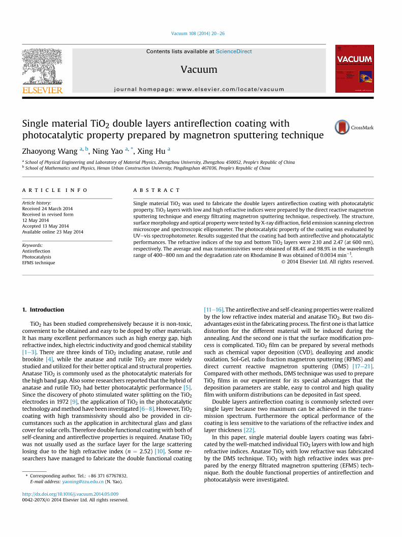
As is observed in Figs. 3 and 4, anatase TiO2 filmwith the lowestrefractive index is deposited at 100 �C. Fig. 5 illustrates thedispersive relations of the films deposited at 100 �C at differentdeposition pressure. The refractive index decreases with theincreasing of the deposition pressure. The highest refractive indexappears at 0.3 Pa with the variation range of 3.02e2.33(350e1000 nm). The lowest refractive index emerges at 3.0 Pa withthe variation range of 2.48e1.96. The refractive index reducesgreatly at the pressure of over 0.75 Pa while little alteration pre-sents at the pressure from 0.3 Pa to 0.75 Pa. The regular pattern of
Table 1Depositing rates and thicknesses of the TiO2 films.
DMS technique (90 min) EFMS technique
Temperature (�C) (0.75 Pa, 0 mesh) Pressure (Pa) (100 �C, 0 mesh) Grid number (mesh) (100 �C, 0.75 Pa)
100 200 300 400 0.3 0.75 1.5 3.0 60 120 280 340 460
Rate (nm min�1) 3.6 3.8 4.8 4.0 3.8 3.6 3.4 3.0 2.3 1.6 1.2 0.8 0.7Thickness (nm) 324 342 432 360 342 324 306 270 121 117 120 118 120
Z. Wang et al. / Vacuum 108 (2014) 20e26 23
the refractive index can be explained by the deposition process inthe DMS technique. As the deposition pressure increases, manyparticles are introduced into the chamber and the mean free pathdecreases for the increased collisions frequency. The kinetic energyof deposition particles also decreases due to the increased colli-sions, which induce a worse combining ability. On the other hand,the discharge current is a function of electron with its density andaverage electron temperature that can be described asI ¼ ne1.7�1(kTe)1/2. According to the quasi-neutrality condition, ne isapproximately equal with nArþ which is proportional to the densityof neutral Ar. So ne is proportional to the deposition pressure. In ourexperiment the current was maintained at 1 A, and ne increaseswith the decline of Te. As a result, the energy being transported tothe substrate decreases and the migration ability becomes poor. Sothe refractive index decreases for the weaker crystallization as thedeposition pressure increased. But the refractive index changeslittle at low pressure of below 0.75 Pa. This is due to the mean freepath that is comparable to the target-substance distance [30].
It is discovered from Table 1 that the depositing rate decreasesas the deposition pressure increases. The highest depositing rate(3.8 nm min�1) is obtained at 0.3 Pa and the lowest depositing of3.0 nm min�1 is generated at 3.0 Pa. According to the above anal-ysis, the declination of the depositing rate is mainly due to theshortened free path of the deposition particles.
According to the structural and optical properties of the TiO2films deposited at different deposition parameters, anatase TiO2film with the lowest refractive index is deposited at 100 �C and3.0 Pa.
3.2. Structural and optical properties of TiO2 films deposited by theEFMS technique
In order to avoid mis-match of the crystal lattice in the prepara-tion of the double layers coating, TiO2 filmwith high refractive indexwas deposited at the same substrate temperature by the EFMS
Fig. 4. Dispersive relations for the refractive indices of TiO2 films deposited at differentsubstrate temperature.
technique. The pressure of 0.75 Pa was chosen as the depositionpressure for the considerationof the results being illustratedbyFig. 5.
Fig. 6 illustrates the structure and refraction indices of TiO2 filmsdeposited by the EFMS technique in which five kinds of grids withdifferentmesh (thenumbers of holes per inch) are used. All thefilmsweredeposited at almost 120nmbycontrolling the deposition time.From Fig. 6(a)we can discover that all thefilms arewell fabricated ofanatase phasewith the samepreferredgrowthorientation at A (101)and there are no obvious difference in the curves, which indicatesthat the crystallinities are similar. It is observed from Fig. 6(b) thatthe refractive index increases with the increasing of the meshnumber. TiO2 film deposited at 460 mesh has the highest refractiveindex ranging from3.11 to2.37 (350e1000nm). Theenergyfiltratingelectrode plays the key role in influencing the structural and opticalproperties of the fabricated film. Being connected with the anode,the energy filtrating electrode absorb high energy ions including Oanions and secondary electrons, which forms the results that boththe overall flux of particles and the bombardment on the substratereduce. The deposition particles with uniform kenotic energy insmaller incident angle can be produced by colliding with the fil-trating electrode. Mean while, the energy flux from positive argonions reaching the substrate can be reduced for the reduced oreliminated anode sheath in front of the substrate by the filtratingelectrode. All the reasons mentioned above provide more time andlower migrating energy for the deposition particles diffusing andgathering on the substrate surface. Thus film containing smallerparticles is fabricated in higher density with higher refractive indexfor the filtrating electrode. Our previouswork reported that ITO filmdeposited by the EFMS technique had smoother surface withcompact structure [23]. Filtrating electrode with larger mesh num-ber causes deeper influence on properties of the deposited film.
It is observed in Table 1 that the depositing rates drop dramat-ically with the increasing of the mesh number. The depositing rateranges from 2.3 nm min�1 to 0.7 nm min�1 with the increasing ofthe mesh number.
400 500 600 700 800 900 1000
2.0
2.2
2.4
2.6
2.8
3.0
Ref
ract
ive
inde
x
Wavelength/nm
0.3 Pa 0.75Pa 1.5 Pa 3.0 Pa
Fig. 5. Dispersive relations of the TiO2 films deposited at different pressure.
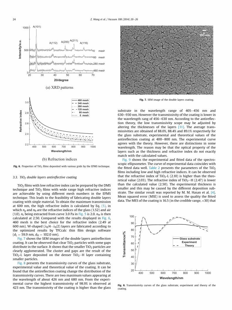
Fig. 6. Properties of TiO2 films deposited with various grids by the EFMS technique.
Fig. 7. SEM image of the double layers coating.
400 500 600 700 800 900 100020
30
40
50
60
70
80
90
100
Tran
smitt
ance
/%
Wavelength/nm
Glass substrate Experiment Theory
Fig. 8. Transmissivity curves of the glass substrate, experiment and theory of thecoating.
Z. Wang et al. / Vacuum 108 (2014) 20e2624
3.3. TiO2 double layers antireflective coating
TiO2 films with low refractive index can be prepared by the DMStechnique and TiO2 films with wide range high refractive indicesare achievable by using different mesh numbers in the EFMStechnique. This leads to the feasibility of fabricating double layerscoating with single material. To obtain the maximum transmissionat 600 nm, the high refractive index is calculated by Eq. (5), inwhich ng and n0 are the refractive indices of the glass (1.52) and air(1.0). nL being extracted from curve 3.0 Pa in Fig. 5 is 2.0. nH is thencalculated at 2.50. Compared with the results displayed in Fig. 6,460 mesh is the best choice for the refractive index (2.49 at600 nm). W-shaped (l0/4�l0/2) layers are fabricated according tothe optimized results by TFCcalc thin film design software(dL ¼ 59.9 nm, dH ¼ 102.0 nm).
Fig. 7 shows the SEM images of the double layers antireflectioncoating. It can be observed that clear TiO2 particles with some gapsdistribute in the surface. It shows that the smaller TiO2 particles areclearly agglomerated. The cluster and gaps are the result of theTiO2-L layer deposited on the denser TiO2eH layer containingsmaller particles.
Fig. 8 presents the transmissivity curves of the glass substrate,experimental value and theoretical value of the coating. It can befound that the antireflection coating change the distribution of thetransmissivity curves. There are two maximum values appearing atthe wavelength of about 426 nm and 680 nm. From the experi-mental curve the highest transmissivity of 98.9% is observed at423 nm. The transmissivity of the coating is higher than the glass
substrate in the wavelength range of 405e456 nm and630e930 nm. However the transmissivity of the coating is lower inthe wavelength rang of 456e630 nm. According to the antireflec-tion theory, the low transmissivity scope may be adjusted byaltering the thicknesses of the layers [31]. The average trans-missivities are obtained of 88.0%, 88.4% and 89.1% respectively forthe glass substrate, experimental and theoretical values of theantireflection coating at 400e800 nm. The experimental curveagrees with the theory. However, there are distinctions in somewavelength. The reason may be that the optical property of thelayers such as the thickness and refractive index do not exactlymatch with the calculated values.
Fig. 9 shows the experimental and fitted data of the spectro-scopic ellipsometer. The curve of experimental data coincides withthe fitted data well. Table 2 presents the parameters of the TiO2films including low and high refractive indices. It can be observedthat the refractive index of TiO2-L (2.10) is higher than the theo-retical value (2.03). The refractive index of TiO2eH (2.47) is lowerthan the calculated value (2.50). The experimental thickness issmaller and this may be caused by the different deposition sub-strate. The similar result was reported by M. M. Hasan et al. [4].Mean squared error (MSE) is used to assess the quality the fitteddata. The MES of the coating is 16.5 (in the credible range, <30) that
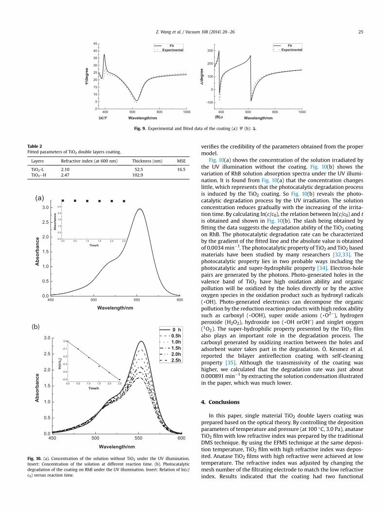
Fig. 9. Experimental and fitted data of the coating (a): J (b): D.
Table 2Fitted parameters of TiO2 double layers coating.
Layers Refractive index (at 600 nm) Thickness (nm) MSE
TiO2-L 2.10 52.5 16.5TiO2eH 2.47 102.9
450 500 550 6000.0
0.5
1.0
1.5
2.0
2.5
3.0
0.0
Abs
orba
nce
Wavelength/nm
Abs
orba
nce
Time/h
450 500 550 6000.0
0.5
1.0
1.5
2.0
2.5
3.0
0.0 0.5 1.0 1.5 2.0 2.5-0.5
-0.4
-0.3
-0.2
-0.1
0.0
ln(c
/c)
Time/h
Abs
orba
nce
Wavelength/nm
0 h 0.5h 1.0h 1.5h 2.0h 2.5h
(b)
(a)
Fig. 10. (a). Concentration of the solution without TiO2 under the UV illumination.Insert: Concentration of the solution at different reaction time. (b). Photocatalyticdegradation of the coating on RhB under the UV illumination. Insert: Relation of ln(c/c0) versus reaction time.
Z. Wang et al. / Vacuum 108 (2014) 20e26 25
verifies the credibility of the parameters obtained from the propermodel.
Fig. 10(a) shows the concentration of the solution irradiated bythe UV illumination without the coating. Fig. 10(b) shows thevariation of RhB solution absorption spectra under the UV illumi-nation. It is found from Fig. 10(a) that the concentration changeslittle, which represents that the photocatalytic degradation processis induced by the TiO2 coating. So Fig. 10(b) reveals the photo-catalytic degradation process by the UV irradiation. The solutionconcentration reduces gradually with the increasing of the irrita-tion time. By calculating ln(c/c0), the relation between ln(c/c0) and tis obtained and shown in Fig. 10(b). The slash being obtained byfitting the data suggests the degradation ability of the TiO2 coatingon RhB. The photocatalytic degradation rate can be characterizedby the gradient of the fitted line and the absolute value is obtainedof 0.0034min�1. The photocatalytic property of TiO2 and TiO2 basedmaterials have been studied by many researchers [32,33]. Thephotocatalytic property lies in two probable ways including thephotocatalytic and super-hydrophilic property [34]. Electron-holepairs are generated by the photons. Photo-generated holes in thevalence band of TiO2 have high oxidation ability and organicpollution will be oxidized by the holes directly or by the activeoxygen species in the oxidation product such as hydroxyl radicals(,OH). Photo-generated electronics can decompose the organicpollution by the reduction reaction products with high redox abilitysuch as carboxyl (,OOH), super oxide anions (,O2�), hydrogenperoxide (H2O2), hydroxide ion (,OH orOH-) and singlet oxygen(1O2). The super-hydrophilic property presented by the TiO2 filmalso plays an important role in the degradation process. Thecarboxyl generated by oxidizing reaction between the holes andadsorbent water takes part in the degradation. €O. Kesmez et al.reported the bilayer antireflection coating with self-cleaningproperty [35]. Although the transmissivity of the coating washigher, we calculated that the degradation rate was just about0.000891min�1 by extracting the solution condensation illustratedin the paper, which was much lower.
4. Conclusions
In this paper, single material TiO2 double layers coating wasprepared based on the optical theory. By controlling the depositionparameters of temperature and pressure (at 100 �C, 3.0 Pa), anataseTiO2 film with low refractive index was prepared by the traditionalDMS technique. By using the EFMS technique at the same deposi-tion temperature, TiO2 film with high refractive index was depos-ited. Anatase TiO2 films with high refractive were achieved at lowtemperature. The refractive index was adjusted by changing themesh number of the filtrating electrode to match the low refractiveindex. Results indicated that the coating had two functional
Z. Wang et al. / Vacuum 108 (2014) 20e2626
properties of both antireflection and photocatalysis. The averagetransmissivity of the antireflection coating was 88.4%(400e800 nm) with the high degradation rate of 0.0034 min�1.Using the same deposition method, single material of TiO2 doublelayers coating with both antireflective and photocatalytic perfor-mances would be a new structure that could be applied in theparticular application.
Acknowledgment
This work is supported in partial by Natural Science Foundationof China (61076041) and Science and Technology Projects of HenanProvince (122102210099, 12B14007).
References
[1] Zhang YL, Guo YD, Zhang GK, Gao YY. Stable TiO2/rectorite: preparation,characterization and photocatalytic activity. Appl Clay Sci 2011;51:335e40.
[2] Aljufairi NH. Energy, electric properties and surface structure of TiO2 for solarcells. Energy 2012;39:6e10.
[3] Pomoni K, Sofianou MV, Georgakopoulos T, Boukos N, Trapalis C. Electricalconductivity studies of anatase TiO2 with dominant highly reactive {001}facets. J Alloys Compd 2013;548:194e200.
[4] Hasan MM, Haseeb ASMA, Saidur R, Masjuki HH, Hamdi M. Influence ofsubstrate and annealing temperatures on optical properties of RF-sputteredTiO2 thin films. Opt Mater 2010;32:690e5.
[5] Meulen TV, Mattson A, €Osterlund L. A comparative study of the photocatalyticoxidation of propane on anatase, rutile, and mixed-phase anatase-rutile TiO2nanoparticles: role of surface intermediates. J Catal 2007;251:131e44.
[6] Wu HB, Hng HH, (David) Lou XW. Direct synthesis of anatase TiO2 nanowireswith enhanced photocatalytic activity. Adv Mater 2012;24:2567e71.
[7] Zhang JW, Fu DF, Gao HY, Deng L. Mechanism of enhanced photocatalysis ofTiO2 by Fe3þ in suspensions. Appl Surf Sci 2011;258:1294e9.
[8] Zhang P, Tian J, Xu RF, Ma GJ. Hydrophilicity, photocatalytic activity andstability of tetraethyl orthosilicate modified TiO2 film on glazed ceramicsurface. Appl Surf Sci 2013;266:141e7.
[9] Fujishima A, Honda K. Electrochemical photolysis of water at a semiconductorelectrode. Nature 1972;238:37e8.
[10] Zhang XT, Fujishima A, Jin M, Emeline AV, Murakami T. Double-layeredTiO2eSiO2 nanostructured films with self-cleaning and antireflective prop-erties. J Phys Chem B 2006;110:25142e8.
[11] Prado R, Beobide G, Marcaide A, Goikoetxea J, Aranzabe A. Development ofmultifunctional solegel coatings: anti-reflection coatings with enhanced self-cleaning capacity. Sol Energy Mater Sol Cells 2010;94:1081e8.
[12] Helsch G, Deubener J. Compatibility of antireflective coatings on glass for solarapplications with photocatalytic properties. Sol Energy 2012;86:831e6.
[13] Li F, Li QM, Kim H. Spray deposition of electrospun TiO2 nanoparticles withself-cleaning and transparent properties onto glass. Appl Surf Sci 2013;276:390e6.
[14] Lu XY, Wang Z, Yang XL, Xu X, Zhang L, Zhao N, et al. Antifogging and anti-reflective silica film and its application on solar modules. Surf Coat Technol2011;206:1490e4.
[15] Liu ZY, Zhang XT, Murakami T, Fujishima A. Sol-gel SiO2/TiO2 bilayer filmswith self-cleaning and antireflection properties. Sol Energy Mater Sol Cells2008;92:1434e8.
[16] Li FT, ZhaoY,HaoYJ,WangXJ, Liu RH, ZhaoDS, et al. N-dopedP25 TiO2-amorphousAl2O3 composites: one-step solution combustion preparation and enhancedvisible-light photocatalytic activity. J Hazard Mater 2012;239e240:118e27.
[17] Lee HJ, Song MY, Jurng JS, Park YK. The synthesis and coating process of TiO2nanoparticles using CVD process. Powder Technol 2011;214:64e8.
[18] Bergamonti L, Alfieri I, Lorenzi A, Montenero A, Predieri G, Barone G, et al.Nanocrystalline TiO2 by solegel: characterisation and photocatalytic activityon Modica and Comiso stones. Appl Surf Sci 2013;282:165e73.
[19] Bayoumi FM, Ateya BG. Formation of self-organized titania nano-tubes bydealloying and anodic oxidation. Electrochem Commun 2006;8:38e44.
[20] Daviðsd�ottir S, Canulescu S, Dirscherl K, Schou J, Ambat R. Investigation ofphotocatalytic activity of titanium dioxide deposited on metallic substrates byDC magnetron sputtering. Surf Coat Technol 2013;216:35e45.
[21] Nair PB, Justinvictor VB, Daniel GP, Joy K, Ramakrishnan V, Thomas PV. Effectof RF power and sputtering pressure on the structural and optical propertiesof TiO2 thin films prepared by RF magnetron sputtering. Appl Surf Sci2011;257:10869e75.
[22] Dhungel SK, Yoo JS, Kim K, Jung SW, Ghosh S, Yi JS. Double-layer antireflectioncoating of MgF2/SiNx for crystalline silicon solar cells. J Korean Phys Soc2006;49:885e9.
[23] Yong WZ, Ning Y, Bao HC, Xing H. Preparation of indium tin oxide anodesusing energy filtrating technique for top-emitting organic light-emittingdiode. Appl Surf Sci 2014;288:604e8.
[24] Macleod HA. Thin film optical filters. Bristol, U.K.: Hilger; 1986.[25] Saleem MR, Silfsten P, Honkanen S, Turunen J. Thermal properties of TiO2
films grown by atomic layer deposition. Thin Solid Films 2012;520:5442e6.[26] Gupta VK, Jain R, Agarwal S, Shrivastava M. Kinetics of photo-catalytic
degradation of hazardous dye tropaeoline 000 using UV/TiO2 in a UVreactor. Colloids Surf A 2011;378:22e6.
[27] Tripathi AK, Singh MK, Mathpal MC, Mishra SK, Agarwal A. Study of structuraltransformation in TiO2 nanoparticles and its optical properties. J Alloys Compd2013;549:114e20.
[28] Shen YM, Yua H, Yao JK, Shao SY, Fan ZX, He HB, et al. Investigation onproperties of TiO2 thin films deposited at different oxygen pressure. Opt LaserTechnol 2008;40:550e4.
[29] Hou YQ, Zhuang DM, Zhang G, Zhao M, Wu MS. Influence of annealing tem-perature on the properties of titanium oxide thin film. Appl Surf Sci 2003;218:98e106.
[30] Zhou W, Zhong XX, Wu XC, Yuan LQ, Shu QW, Xia YX. Structural and opticalproperties of titanium oxide thin films deposited on unheated substrate atdifferent total pressures by reactive dc magnetron sputtering with a substratebias. J Korean Phys Soc 2006;49:2168e75.
[31] Moys BA. The theory of double-layer antireflection coatings. Thin Solid Films1974;21:145e57.
[32] Libanori R, Giraldi TR, Longo E, Leite ER, Ribeiro C. Effect of TiO2 surfacemodification in rhodamine B photo degradation. J SoleGel Sci Technol2009;49:95e100.
[33] Zhang YP, Pan CX. TiO2/graphene composite from thermal reaction ofgrapheme oxide and its photocatalytic activity in visible light. J Mater Sci2011;46:2622e6.
[34] Guan K. Relationship between photocatalytic activity, hydrophilicity and self-cleaning effect of TiO2/SiO2 films. Surf Coat Technol 2005;191:155e60.
[35] Kesmez €o, çamurlu HE, Burunkaya E, Arpaç E. Sol-gel preparation and char-acterization of anti-reflective and self-cleaning SiO2eTiO2 double-layernanometric films. Sol Energy Mater Sol Cells 2009;93:1833e9.
Related Documents