1 Carbon Nanotubes as Electron Gun Sources Mark Mann 1 PROPERTIES OF CARBON NANOTUBES There has been extensive research into the properties, synthesis and possible applications of carbon nanotubes (CNTs) since they came to prominence following the Iijima paper [1] of 1991. 1.1 THE STRUCTURE AND PROPERTIES OF THE CARBON NANOTUBE Carbon nanotubes are composed of sp 2 covalently-bonded carbon in which graphene walls are rolled up cylindrically to form tubes. The ends can either be left open, which is an unstable configuration due to incomplete bonding, they can be bonded to a secondary surface, not necessarily of carbon, or they can be capped by a hemisphere of sp 2 carbon, with a fullerene-like structure [2]. In terms of electrical properties, single-walled CNTs can be either semiconducting or metallic and this depends upon the way in which they roll up, as illustrated in Fig. 1.1. Multi-walled CNTs are non-semiconducting (i.e. semi-metallic like graphite) in nature. Their diameters range from 2 to 500 nm, and their lengths range from 50 nm to a few mm. Multi-walled CNTs contain several concentric, coaxial graphene cylinders with interlayer spacings of ~0.34 nm [3]. This is slightly larger than the single crystal graphite spacing which is 0.335 nm. Studies have recently shown that the intershell spacing can range from 0.34 to 0.39 nm, where the intershell spacing decreases with increasing CNT diameter with a pronounced effect in smaller diameter CNTs (such as those smaller than 15 nm) as a result of the high curvature in the graphene sheet [4,5]. As each cylinder has a different radius, it is impossible to line the carbon atoms up within the sheets as they do in crystalline graphite. Therefore, multi-walled CNTs tend to exhibit properties of turbostratic graphite in which the layers are uncorrelated. For instance, in highly crystallized multi-walled CNTs, it has been shown that if contacted externally, electric current is conducted through only the outermost shell [6].

Welcome message from author
This document is posted to help you gain knowledge. Please leave a comment to let me know what you think about it! Share it to your friends and learn new things together.
Transcript

1 Carbon Nanotubes as Electron Gun Sources Mark Mann
1 PROPERTIES OF CARBON NANOTUBES
There has been extensive research into the properties, synthesis and possible
applications of carbon nanotubes (CNTs) since they came to prominence following
the Iijima paper [1] of 1991.
1.1 THE STRUCTURE AND PROPERTIES OF THE CARBON
NANOTUBE
Carbon nanotubes are composed of sp2 covalently-bonded carbon in which graphene
walls are rolled up cylindrically to form tubes. The ends can either be left open, which
is an unstable configuration due to incomplete bonding, they can be bonded to a
secondary surface, not necessarily of carbon, or they can be capped by a hemisphere
of sp2 carbon, with a fullerene-like structure [2]. In terms of electrical properties,
single-walled CNTs can be either semiconducting or metallic and this depends upon
the way in which they roll up, as illustrated in Fig. 1.1.
Multi-walled CNTs are non-semiconducting (i.e. semi-metallic like graphite) in
nature. Their diameters range from 2 to 500 nm, and their lengths range from 50 nm
to a few mm. Multi-walled CNTs contain several concentric, coaxial graphene
cylinders with interlayer spacings of ~0.34 nm [3]. This is slightly larger than the
single crystal graphite spacing which is 0.335 nm. Studies have recently shown that
the intershell spacing can range from 0.34 to 0.39 nm, where the intershell spacing
decreases with increasing CNT diameter with a pronounced effect in smaller diameter
CNTs (such as those smaller than 15 nm) as a result of the high curvature in the
graphene sheet [4,5]. As each cylinder has a different radius, it is impossible to line
the carbon atoms up within the sheets as they do in crystalline graphite. Therefore,
multi-walled CNTs tend to exhibit properties of turbostratic graphite in which the
layers are uncorrelated. For instance, in highly crystallized multi-walled CNTs, it has
been shown that if contacted externally, electric current is conducted through only the
outermost shell [6].

Chapter 1 Carbon Nanotubes and their Properties 2
Figure 1.1: (top) A graphene sheet rolled up to obtain a single-walled CNT. (bottom)
The map shows the different single-walled CNT configurations possible. Were the
graphene sheet to roll up in such a way that the atom at (0,0) would also be the atom
at (6,6), then the CNT would be metallic. Likewise, if the CNT wrapped up so that the
atom at (0,0) was also the atom at (6,5), the CNT would be semi-conducting. The
small circles denote semiconducting CNTs and the large circles denote non-
semiconducting CNTs. Two thirds of CNTs are semi-conducting and one third
metallic [7].
CNTs typically have a Young’s Modulus ~10 times that of steel [8] and an electrical
conductivity many times that of copper [9]. Some important properties of CNTs are
listed in table 1.1.
3 Carbon Nanotubes as Electron Gun Sources Mark Mann
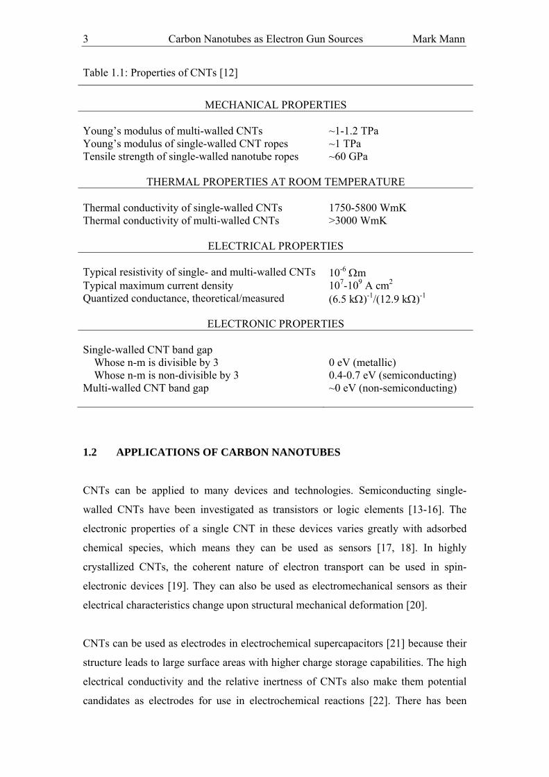
Table 1.1: Properties of CNTs [12]
MECHANICAL PROPERTIES
Young’s modulus of multi-walled CNTs
~1-1.2 TPa
Young’s modulus of single-walled CNT ropes ~1 TPa Tensile strength of single-walled nanotube ropes
~60 GPa
THERMAL PROPERTIES AT ROOM TEMPERATURE Thermal conductivity of single-walled CNTs
1750-5800 WmK
Thermal conductivity of multi-walled CNTs
>3000 WmK
ELECTRICAL PROPERTIES Typical resistivity of single- and multi-walled CNTs
10-6 Ωm
Typical maximum current density 107-109 A cm2
Quantized conductance, theoretical/measured
(6.5 kΩ)-1/(12.9 kΩ)-1
ELECTRONIC PROPERTIES Single-walled CNT band gap
Whose n-m is divisible by 3 0 eV (metallic) Whose n-m is non-divisible by 3 0.4-0.7 eV (semiconducting) Multi-walled CNT band gap
~0 eV (non-semiconducting)
1.2 APPLICATIONS OF CARBON NANOTUBES
CNTs can be applied to many devices and technologies. Semiconducting single-
walled CNTs have been investigated as transistors or logic elements [13-16]. The
electronic properties of a single CNT in these devices varies greatly with adsorbed
chemical species, which means they can be used as sensors [17, 18]. In highly
crystallized CNTs, the coherent nature of electron transport can be used in spin-
electronic devices [19]. They can also be used as electromechanical sensors as their
electrical characteristics change upon structural mechanical deformation [20].
CNTs can be used as electrodes in electrochemical supercapacitors [21] because their
structure leads to large surface areas with higher charge storage capabilities. The high
electrical conductivity and the relative inertness of CNTs also make them potential
candidates as electrodes for use in electrochemical reactions [22]. There has been

Chapter 1 Carbon Nanotubes and their Properties 4
research into using CNTs to store hydrogen [23] though the amount stored is not as
high as originally anticipated [24]. CNTs mechanically deflect upon electric
stimulation which opens up the possibility of their application in cantilevers and
actuators [21]. There has also been extensive work on their application in composites
which utilize their physical strength and small size. Here single-walled CNTs are
favoured as they are more flexible whilst still very strong [25].
In the near term, however, the CNT applications most likely to come to market first
are their employment in various electron sources. There are three main types of
electron emission: thermionic emission, field emission, or a mixture of the two. The
next section will focus on the various applications of electron sources, which type of
emission they use and their relative merits together with an in depth look at field
emission.
1.3 ELECTRON EMISSION APPLICATIONS
Electron sources are employed in a wide range of technologies which include displays
[26], telecommunication devices [27], electron-beam imaging equipment [28] and
microwave amplifiers [29]. The most widely employed electron source is still the
thermionic cathode used in television cathode-ray tubes and high-power microwave
amplifiers, though its popularity is on the decline with the advent of flat-panel
displays. Thermionic emission occurs when a charged metal or a charged metal oxide
surface is heated. The thermal vibrational energy gained by the electrons overcomes
the electrostatic forces holding them to the surface. The electrons are released into
vacuum from the surface and the resultant beam is controlled by a sequence of fields.
The temperature of operation is typically 2000 K: an undesirable requirement as this
results in an inefficient consumption of power. Though you can get thin CRTs at
present, the vacuum tube required is typically quite large, which has also contributed
to its decline in popularity. Demand has pushed the requirements of the electron
source to smaller and smaller scales to increase efficiency and to open up
opportunities for alternative electron source applications. As well as flat-panel
displays, new applications include parallel electron-beam microscopy and
5 Carbon Nanotubes as Electron Gun Sources Mark Mann
nanolithography, compact microwave amplifiers and portable X-ray tubes. These
applications have motivated worldwide research into alternative smaller, more
efficient electron source technologies.
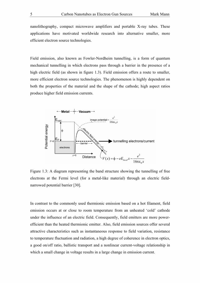
Field emission, also known as Fowler-Nordheim tunnelling, is a form of quantum
mechanical tunnelling in which electrons pass through a barrier in the presence of a
high electric field (as shown in figure 1.3). Field emission offers a route to smaller,
more efficient electron source technologies. The phenomenon is highly dependent on
both the properties of the material and the shape of the cathode; high aspect ratios
produce higher field emission currents.
Figure 1.3: A diagram representing the band structure showing the tunnelling of free
electrons at the Fermi level (for a metal-like material) through an electric field-
narrowed potential barrier [30].
In contrast to the commonly used thermionic emission based on a hot filament, field
emission occurs at or close to room temperature from an unheated ‘cold’ cathode
under the influence of an electric field. Consequently, field emitters are more power-
efficient than the heated thermionic emitter. Also, field emission sources offer several
attractive characteristics such as instantaneous response to field variation, resistance
to temperature fluctuation and radiation, a high degree of coherence in electron optics,
a good on/off ratio, ballistic transport and a nonlinear current-voltage relationship in
which a small change in voltage results in a large change in emission current.
Chapter 1 Carbon Nanotubes and their Properties 6
However, to extract a current significant enough to be used for the aforementioned
applications, field emission requires a very large local field of a few V/nm. A typical
method employed to attain this high field is to use a very sharp needle, such as
tungsten, with the apex chemically etched to a few hundred nanometres. Even so, with
this geometry, a few thousand volts still needs to be applied macroscopically in order
to draw a useable current (eg. the extraction voltage of a field emission electron
microscope is 1-5 kV). Field emission will be discussed in greater detail later in this
section.
1.3.1 MOTIVATION FOR CARBON NANOTUBE EMITTERS
Much research has been focused on the application of CNTs to field emission sources
because they have several advantages over other field-emitting materials.
Firstly, when compared with other commonly used emitters such as tungsten, the
CNT’s covalent bonds are much stronger than tungsten’s metallic bonds. As a result,
the activation energy for surface migration and diffusion of the emitter atoms is much
larger than for a tungsten electron source, making it much more unlikely. Therefore,
the tip can withstand the extremely strong fields (several V/nm) needed for field
emission. Related to this point, nanotubes can be very stable emitters, even at high
temperatures. Purcell et al [31] demonstrated that a multi-walled carbon nanotube
emitter could be heated by its field-emitted current up to 2000K and remain stable.
They claimed that this was the first reported observation of field emission induced
stable heating. This characteristic is distinctly different from metal emitters. In metals,
the resistance, R, increases with temperature, which means that more heat, Q, is
produced as higher currents, I, are drawn (Q = I2R). The combination of high
temperature and electric field causes the well known mechanism of field-sharpening
of tips by surface diffusion, which in turn increases the local field, current and
temperature. This positive feedback mechanism causes an unstable thermal runaway
which inevitably leads to emitter destruction for metal-based emitters. In contrast, the
resistance of a nanotube decreases with temperature which limits I2R heat generation.
Consequently, its temperature varies sub-linearly with current.
7 Carbon Nanotubes as Electron Gun Sources Mark Mann
Secondly, when compared with other film field emitters such as diamond or
amorphous carbon structures, CNTs have a high aspect ratio, a small radius of
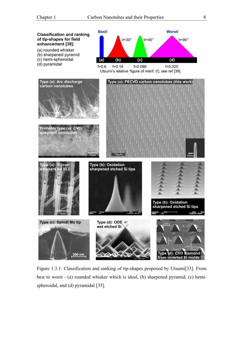
curvature of the cap and good conductance [32]. Utsumi [33] evaluated commonly
used field emission tip shapes as shown in Figure 1.3.1, and concluded that the best
field emission tip should be whisker-like, followed by the sharpened pyramid, hemi-
spheroidal, and pyramidal shapes. Indeed, nanotubes are whisker-like. It has been
reported that even curly ‘spaghetti-like’ nanotubes stand up vertically like whiskers
during emission under the application of an electric field [34].
Thirdly, because of the CNT’s extremely large Young’s modulus and maximal tensile
strength, they are able to withstand the high fields around them and current densities
coming from within.
Fourthly, the graphene walls in them are parallel to the filament axis resulting in the
nanotubes (whether metallic single-walled or multi-walled) exhibiting high electrical
conductivity at room temperature.
Finally, carbon has one of the lowest sputter coefficients [35], which is an advantage
as an electron source is usually bombarded by positive ions.
Chapter 1 Carbon Nanotubes and their Properties 8
Figure 1.3.1: Classification and ranking of tip-shapes proposed by Utsumi[33]. From
best to worst - (a) rounded whisker which is ideal, (b) sharpened pyramid, (c) hemi-
spheroidal, and (d) pyramidal [35].

9 Carbon Nanotubes as Electron Gun Sources Mark Mann
1.3.2 CARBON NANOTUBE FIELD EMISSION APPLICATIONS
Figure 1.3.2: Applications, such as lamps, X-ray source and field emission displays,
using carbon nanotubes (CNT) as the field emission electron source [36].
Research groups have recently been focusing on the controlled production of micro-
field emission sources based on carbon nanotubes. Such electron sources could be
used in microguns for electron microscopy and parallel electron beam lithography, but
are also equally applicable to ‘macroscopic’ applications such as field emission
displays, microwave amplifiers and X-ray sources. Examples of these are shown in
figure 1.3.2. This thesis focuses on their use as sources in electron microscopy, but
other applications will be outlined first.

Chapter 1 Carbon Nanotubes and their Properties 10
1.3.2.1 FIELD EMISSION DISPLAYS
The application area of CNT electron sources with the largest potential market is the
flat-panel field-emission display [37, 38], which provides a high-brightness display
for both consumer and professional applications. Figure 1.3.2.1 shows the functions of
the simplest form of a display pixel. Nanotubes are patterned on a matrix of electrodes
in a vacuum housing. The counter electrode is a glass plate coated with a conducting
but transparent layer and a phosphor layer. A voltage difference of a few kilovolts
between the nanotube cathode and the glass plate results in field emission and the
generation of light through excitation of the cathodoluminescent phosphor. An image
can be obtained by addressing selectively the different positions of the matrix, which
can either be monochrome or in colour if each pixel is divided in red, blue and green
sub-pixels.
Figure 1.3.2.1: Schematic of the working principle of a field-emission display pixel:
(a) diode structure; (b) triode structure with ballast resistor in series with the emitters;
(c) image of a prototype of a CNT field-emission display [39] with a gate structure, an
active area of 38” in diagonal, full colour and 100 Hz.
Problems include the large voltage difference required between the cathode and the
anode to operate the display, which is needed both for extracting electrons and to
maximize efficiency in the phosphor. Also, it is probable that each pixel requires a
different gate voltage and so every pixel must be current regulated individually to
dV0
V0
Vg
danode
gate
cathode
(a)
(b)
(c)

11 Carbon Nanotubes as Electron Gun Sources Mark Mann
obtain stable emission. CNTs incorporated directly onto the electrodes are likely to
degrade. CNTs would need lifetimes of several years on the electrode for the display
to be viable.
1.3.2.2 CARBON NANOTUBES APPLIED TO GATED CATHODES FOR
PARALLEL ELECTRON BEAM LITHOGRAPHY
If the same principle used in field emission displays is applied to electron beam
lithography, but with only one CNT as an electron source, then an array of parallel
gates could be used to speed up parallel-write electron beam lithography. With several
electron beams acting in parallel, this would vastly decrease the time it takes to write
electron beam patterns onto silicon chips with lithography. It would also enable an
increase in resolution because CNTs tend to be smaller than typical electron sources
used for lithography. Figure 1.3.2.2 shows what a typical array of electron sources
might look like.
Carbon nanotubes are an ideal electron source for such a novel parallel e-beam
lithography system, but currently, more work is still needed to increase the yield of
functioning cathodes.

Chapter 1 Carbon Nanotubes and their Properties 12
Figure 1.3.2.2: (a) An array of carbon nanotubes, with a 5 µm pitch. (b) Top view of
the integrated gate carbon nanotube cathode. The pitch of the gate apertures is 5 µm.
The nanotube appears as a bright dot in each gate aperture. (c) Cross section SEM
view of the integrated gate carbon nanotube cathode, showing the gate electrode,
insulator, emitter electrode, and vertically standing nanotube [40].
1.3.2.3 CARBON NANOTUBES AS COLD MICROWAVE AMPLIFIERS
Current microwave amplifiers use electron sources that operate thermionically and
use a lot of power. An alternative method for microwave amplification reported
recently [41] incorporates a microwave diode that instead uses a cold-cathode electron

13 Carbon Nanotubes as Electron Gun Sources Mark Mann
source consisting of a CNT array which operates at high frequency and at high current
densities. As field emission sources are smaller and weigh less, the reduction in power
and mass would make satellite transponders much cheaper.
1.3.2.4 OTHER FIELD EMISSION APPLICATIONS
Field emission from CNTs has been employed in X-ray sources [42], where a film of
CNTs is used as the cathode. They have also been employed in field emission lamps
[38], where CNTs are again used as a cathode. They can also be used as an emitting
CNT in an electrically driven mechanical resonator [31], and high precision thrusters
for space telescopes [43].
1.4 ELECTRON GUN SOURCES
Electron microscopy demands a bright, stable, low-noise electron source with a low
kinetic energy spread in order to maximise spatial resolution and contrast. Recent
research, detailed later in this section, has investigated whether the carbon nanotube
can act as an improved electron source for this application and how it compares to the
best electron sources available today.
1.4.1 CURRENT MICROSCOPY ELECTRON SOURCE TECHNOLOGY
An electron gun is the source of electrons in the electron microscope. Figure 1.4.1
shows a typical microscope with the source denoted. The beam is focused by a system
of lenses and then rastered across a sample by a quadrupole. Either secondary
electrons are detected above the sample as in a scanning electron microscope (SEM)
or transmitted electrons are detected on the other side of the sample as in a
transmission electron microscope (TEM). The quality of all these components

Chapter 1 Carbon Nanotubes and their Properties 14
ultimately determines the quality of the image obtained from an electron microscope,
and manufacturers are continually addressing these factors to improve resolution.
The quality of the electron source itself is a contributing factor. The source’s various
attributes combined determine the resolution a microscope can attain. These are: the
stability of the electron beam, the kinetic energy spread of electrons within the beam,
the virtual source size (which is related to the area on the tip that the electron are
emitted from), and the reduced brightness which determines how much current can be
extracted for a given voltage. These will be discussed in greater detail later in the
chapter.
Figure 1.4.1: Schematic cross-section of a typical electron microscope. The electron
source is inserted into the area marked ‘gun,’ a voltage or power source applied and
an electron beam extracted by the anode.
15 Carbon Nanotubes as Electron Gun Sources Mark Mann
Different electron sources can be used to maximise one or two of these attributes,
sacrificing the others when targeted towards a particular application. These properties
are material-dependent and the various electron sources currently available on the
market are discussed below [44, 45].
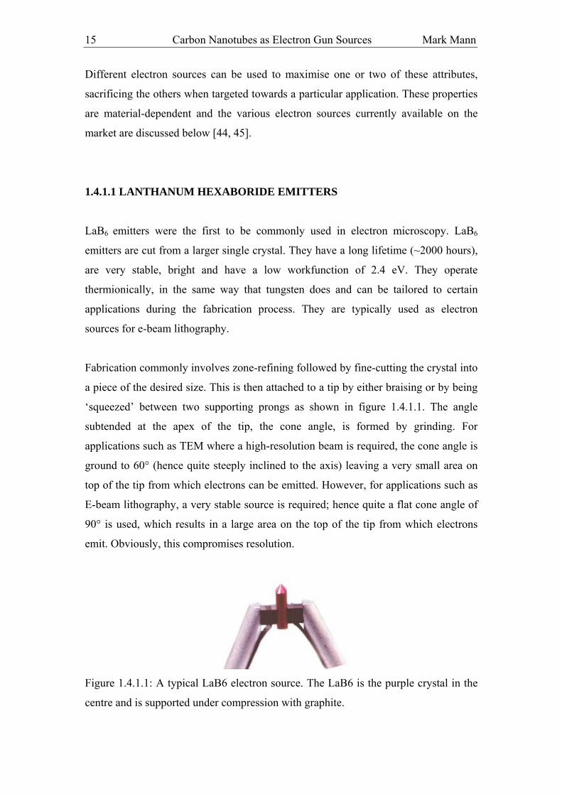
1.4.1.1 LANTHANUM HEXABORIDE EMITTERS
LaB6 emitters were the first to be commonly used in electron microscopy. LaB6
emitters are cut from a larger single crystal. They have a long lifetime (~2000 hours),
are very stable, bright and have a low workfunction of 2.4 eV. They operate
thermionically, in the same way that tungsten does and can be tailored to certain
applications during the fabrication process. They are typically used as electron
sources for e-beam lithography.
Fabrication commonly involves zone-refining followed by fine-cutting the crystal into
a piece of the desired size. This is then attached to a tip by either braising or by being
‘squeezed’ between two supporting prongs as shown in figure 1.4.1.1. The angle
subtended at the apex of the tip, the cone angle, is formed by grinding. For
applications such as TEM where a high-resolution beam is required, the cone angle is
ground to 60° (hence quite steeply inclined to the axis) leaving a very small area on
top of the tip from which electrons can be emitted. However, for applications such as
E-beam lithography, a very stable source is required; hence quite a flat cone angle of
90° is used, which results in a large area on the top of the tip from which electrons
emit. Obviously, this compromises resolution.
Figure 1.4.1.1: A typical LaB6 electron source. The LaB6 is the purple crystal in the
centre and is supported under compression with graphite.

Chapter 1 Carbon Nanotubes and their Properties 16
LaB6 emitters, however, are becoming less popular. They commonly have a large
energy spread of 1 eV and are not very bright (107 A/cm2SR). Customers purchasing
electron microscopes often opt for tungsten thermionic emitters even though they
have much shorter lifetimes.
1.4.1.2 THE TUNGSTEN THERMIONIC EMITTER
Tungsten thermionic emitters in essence have virtually the same properties as LaB6.
However, tungsten emitters only last for ~100 hours, whereas LaB6 emitters can last
for months. They also have a large source size (>104 atoms) due to their shape, and
are even less bright than LaB6 emitters (106 A/cm2SR).
However, they are favoured because of their simplicity of manufacture. The emitter
consists of a wire filament bent into the shape of a hairpin which is attached to a
thicker metal support (see figure 1.4.1.2). The filament operates at ~2700 K by
resistive heating. The tungsten cathodes are widely used because they are both reliable
and inexpensive. Lateral resolution is limited because the tungsten cathode current
densities are only about 1.75 A/cm2.
Figure 1.4.1.2: A schematic diagram of a typical tungsten hairpin thermionic emitter
(courtesy of Barry Scientific Inc, Fiskdale, MA, USA). The hairpin is quite large,
which results in electron emission coming from a very large area. Consequently, the
resultant current is relatively weak.

17 Carbon Nanotubes as Electron Gun Sources Mark Mann
The fabrication of a LaB6 emitter is more convoluted, so this will increase the price.
The other advantage of the tungsten emitter over the LaB6 emitter is that the latter can
often fall off as it is only held by pressure.
1.4.1.3 THE SCHOTTKY EMITTER
The Schottky emitter is made out of single crystal tungsten and is coated with a thin
layer of zirconium oxide. Zirconium oxide is added to the tungsten tip to reduce the
workfunction. A low workfunction is desirable, as this will result in a low kinetic
energy spread at high temperatures. It is designed to operate within definite
temperature boundaries over time. The range is typically 1750-1800 K. The source
size is typically 15 nm, the energy spread low ~0.3 eV. It is brighter than both
thermionic emitters with a typical brightness of 5 × 10⁸ A/cm2SR and has a stability
of less than 1%. They also last a very long time (1-2 years is typical). Interestingly,
Schottky emitters increase in noise with time (the timeframe being over the period of
a year). The mechanics of this are not yet clearly understood.
A single crystal tungsten wire, typically of 100 μm diameter and 5 mm long is spot-
welded to a tungsten crosswire of similar dimensions which in turn is attached to two
thick covar (a metal alloy) prongs, as shown in the schematic in figure 1.4.1.3.1. It is
vitally important in this process that all parts of the electron column, especially the
electron source are aligned along a single beam-axis. Consequently, many checking
steps are carried out during the fabrication process. Tips that are not aligned to within
2 μm of the vertex of the crosswire are discarded.

Chapter 1 Carbon Nanotubes and their Properties 18
Figure 1.4.1.3.1: Schematic of a tip made at FEI in Oregon. The ceramic base holds
two metal prongs, with a crosswire connecting the two. At the vertex of the crosswire,
the tip is attached. This should be attached with the whole shaft of the tip centrally
located on-axis so it can be aligned with the rest of the column. The suppressor (in
dark grey) is also shown on this diagram. It is fixed to the ceramic base by grub
screws under compression.
To obtain a sharp tip, the tip is inverted and etched in NaOH solution. There are
various factors that can affect the repeatability of this process, so it is important to
minimise the effect of these factors. For instance, the temperature of the solution must
remain constant. Therefore, the etchant is placed in a bath which can control the
temperature to the nearest °C. Air and solution currents can also affect the etching as
can the depth to which the wire is held below the meniscus of the solution and the
etchant concentration. There are also two etching stages to maximise repeatability.
Tips produced at FEI typically measure 150 nm across with a constantly maintained
cone angle. Once etching is complete, the remnants of sodium hydroxide are removed
by dipping in alcohols and boiling water. This step must be highly repeatable, so great
care is taken to ensure that all experimental parameters are kept constant. The tip is
then mounted in a gun module.
19 Carbon Nanotubes as Electron Gun Sources Mark Mann
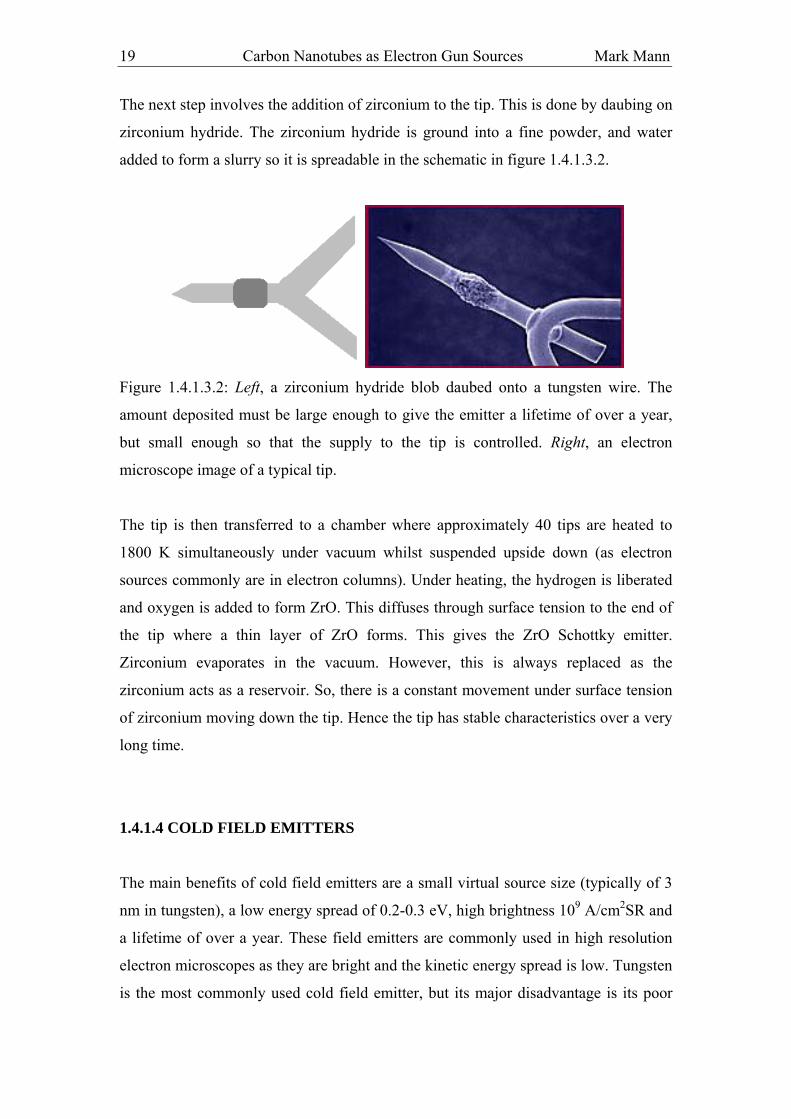
The next step involves the addition of zirconium to the tip. This is done by daubing on
zirconium hydride. The zirconium hydride is ground into a fine powder, and water
added to form a slurry so it is spreadable in the schematic in figure 1.4.1.3.2.
Figure 1.4.1.3.2: Left, a zirconium hydride blob daubed onto a tungsten wire. The
amount deposited must be large enough to give the emitter a lifetime of over a year,
but small enough so that the supply to the tip is controlled. Right, an electron
microscope image of a typical tip.
The tip is then transferred to a chamber where approximately 40 tips are heated to
1800 K simultaneously under vacuum whilst suspended upside down (as electron
sources commonly are in electron columns). Under heating, the hydrogen is liberated
and oxygen is added to form ZrO. This diffuses through surface tension to the end of
the tip where a thin layer of ZrO forms. This gives the ZrO Schottky emitter.
Zirconium evaporates in the vacuum. However, this is always replaced as the
zirconium acts as a reservoir. So, there is a constant movement under surface tension
of zirconium moving down the tip. Hence the tip has stable characteristics over a very
long time.
1.4.1.4 COLD FIELD EMITTERS
The main benefits of cold field emitters are a small virtual source size (typically of 3
nm in tungsten), a low energy spread of 0.2-0.3 eV, high brightness 109 A/cm2SR and
a lifetime of over a year. These field emitters are commonly used in high resolution
electron microscopes as they are bright and the kinetic energy spread is low. Tungsten
is the most commonly used cold field emitter, but its major disadvantage is its poor

Chapter 1 Carbon Nanotubes and their Properties 20
stability, which has been said to be as much as 6%. That said, there is confusion over
what “stability” means. This will be discussed in further detail in chapter four. The
reason for poor stability is the metallic nature of the bonding in tungsten. Metallic
bonds are not as strong as ionic or covalent bonds. Upon application of a high electric
field, atoms on the tungsten tip can move around the tip, thus changing the shape of
the tip which results in alteration of the field which in turn leads to current oscillation.
The tungsten tips are fabricated using the same method as in Schottky emitters,
though etch conditions will be changed to obtain tips that are 40 nm in radius. It is
desirable to find a field emitter that is more stable over long periods.
1.4.2 TIP CHARACTERISATION
All tips sold by the electron beam industry are characterised prior to delivery. Tips are
mounted in a suppressor and extractor setup, and then fitted into a gun module for
testing (complete with Faraday cup). All the important properties of the emitter are
determined and included on a datasheet for each tip. The properties of all the tips
discussed are summarized in a table 1.4.2.
Table 1.4.2: A summary of the various types of electron source. The cold field emitter
refers to tungsten and the tungsten emitter values refer to its thermionic properties
[44,45].
Schottky
Cold Field
LaB6
Tungsten
Source size (nm)
15
3
104
> 104
Energy spread (eV) 0.3-1.0 0.2-0.3 1.0 1.0 Brightness (A/cm2SR) 5 × 10⁸ 109 107 106
Short-term stability % < 1 4-6 < 1 < 1 Service life > 1 year > 1 year 2000 hours 100 hours Workfunction (eV)
~2.3 ~4.5 eV ~2.5 eV 4.5 eV
21 Carbon Nanotubes as Electron Gun Sources Mark Mann
Characterisation takes about 10 minutes per tip, so to increase efficiency 10 are done
in one cycle which is one of the benefits of scaling a process up to factory production.
As an indication of the numbers involved, FEI Company typically manufacture 100
Schottky emitters a week with approximately 70 % considered fit for sale.
1.4.3 TIP ALIGNMENT
It is important to have alignment of the tip, as any error in the beam alignment will be
magnified through all the various lens corrections down the column. This is a major
cause of astigmatism. Alignment is checked using a simple microscope with a large
screen projection. The axis alignment is tested first. The tip, commonly sitting on a
crosswire attached to prongs through a ceramic (see figure 1.4.1.2), is placed in a
simple stand horizontally and rotated through 360°. The extremities of deviation are
noted and if the range of the deviation is greater than 2 μm, the tip is discarded.
The tip is exposed to high temperatures and current throughout the tip’s life, which for
the case of the Schottky emitters, can be years. As a consequence, the shape and
structure of the tip is likely to change over this time and it is desirable to know the
extent of such changes. Therefore, many measurements of the tip’s dimensions are
made using this simple microscope setup (as it can measure to the nearest 10,000th of
an inch) to see the change after the tip has been used for some time.
1.4.4 ALIGNMENT IN THE COLUMN
The whole electron column is specifically designed so that everything slots into place.
The column is designed so that there is a manoeuvrability of about 5 μm to ensure that
lenses, electron sources and differential pumps are aligned so that the electron beam
can travel through to the sample without deflection. Differential pumps consist of a
small hole or tube whose dimensions are determined by a set of equations that
determine flow rates between chambers at different pressures. For instance, the
electron source itself is commonly at 10-9 mBar, the electron column at 10-7 mBar, and

Chapter 1 Carbon Nanotubes and their Properties 22
the sample chamber 10-6 mBar. It typically takes 3-5 days to construct a completely
new column and make it fully operational.
1.5 FIELD EMISSION PROPERTIES OF CARBON NANOTUBES
It is straightforward to see how CNTs are good candidates for standard field emission
applications used in displays, but it is important to understand in more detail why
carbon nanotubes are desirable for high-quality field emission sources. Only recently
has detailed research into field emission from nanotubes been carried out. Amongst
the first to look into nanotube field emission properties was Martijn Fransen whose
thesis [46] included detailed investigations and comparisons of the materials used for
field emission in electron guns currently available. In the final chapter, he found a
source that was as bright as the ZrO Schottky emitter (which is considered to be the
brightest electron gun material available at the moment), yet a more stable source with
a significantly lower kinetic energy spread than the W emitter, currently used to
obtain higher resolutions.
Further and much more detailed investigations were carried out by de Jonge et al [47].
As well as determining the typical characteristics of field emitters such as brightness,
kinetic energy spread etc, it was also important to conclusively determine whether the
emission was coming from the nanotube itself. This section will outline Fowler-
Nordheim theory and will detail the various properties of electron beams which are
used to determine the feasibility of electron sources and discuss whether the CNT is a
viable alternative source.
1.5.1 FOWLER-NORDHEIM THEORY
Field emission is the quantum-mechanical tunnelling of electrons from a surface into
vacuum in response to a very high electric field. In a material, electrons at the Fermi
level must overcome the potential barrier imposed by the workfunction, φ, before they
can escape into vacuum. In the presence of an external electric field, the external

23 Carbon Nanotubes as Electron Gun Sources Mark Mann
potential barrier V(x) is modified as shown in Figure 1.3. For typical metals (φ ~ 4.5
eV), field emission occurs when the barrier width is reduced to a few nanometres
under an applied electric field, Elocal, of a few V/nm. Due to the quantum-mechanical
uncertainty in the electron position, electrons are able to tunnel across this narrow
barrier. As the field increases, the barrier width decreases resulting in more electrons
tunnelling across the barrier. Typically, detectable tunnelling current occurs where
Elocal > 3 V/nm.
For any material, the tunnelling current density is given by integrating the product of
the electron transmission probability through the barrier, T(E), and the incident supply
of electrons, N(E), over the range of potential energies. Physically, T(E) depends on
the barrier width, which in turn depends on the field applied and the work function of
the material. N(E) depends on the band structure of the material and the distribution of
electrons at a particular temperature. By assuming a metallic free-electron band
structure at 0 K, the variation of current with field from a field emitter is dictated by
the Fowler-Nordheim (FN) theory of field emission [48], where the current density J
can be expressed as:
⎭⎬⎫
⎩⎨⎧−
⎪⎭
⎪⎬⎫
⎪⎩
⎪⎨⎧
=F
caccabFcJ
2/3
2132221
2
1 exp1exp φφφ
Eq. 1.5.1.1
with workfunction φ and electric field F. The constants were determined elsewhere
[49] and defined as
a1 = 0.958
a2 = 1.05
b1 = 1.05
c1 = e3/8πh
c2 = 8π√(2m)/3he
c3 = e3/4πε0
with the electron charge e, Planck’s constant h, electron mass m and the permittivity
of free space ε0 taking their usual values. The local field at the apex of a sharp,

Chapter 1 Carbon Nanotubes and their Properties 24
electrically conducting tip equals the product of the extraction voltage U and the field
enhancement factor β:
F = βU Eq. 1.5.1.2
The value of β can be computed numerically if the geometry of the emitter [48] is
known.
A graph of logI/U2 versus 1/U, the FN plot, is therefore a linear curve. This was
found to be the case when field-emission measurements were taken of nanotubes
attached to tips. De Jonge et al. repeated the measurements for eight tips, (the first of
which is shown in Figure 1.5.1). TEM images of the nanotubes had found that most
CNTs had a few walls and a radius of between 1 and 3 nm, which was consistent with
the values that they obtained from the FN plots.
Figure 1.5.1: Emission measurements of a typical CNT electron source for T = 800 K
in a vacuum of 3 × 10⁻¹⁰ mBar. (a) Field emission pattern recorded with a micro
channel plate and a phosphor screen. (b) FN plot and a linear fit with a slope of -3244
(dashed). Figure courtesy of de Jonge.

25 Carbon Nanotubes as Electron Gun Sources Mark Mann
1.5.2 MEASUREMENT OF THE ENERGY SPECTRUM
The current density function J(E) as a function of the energy E is given by:
( )⎟⎟⎠
⎞⎜⎜⎝
⎛
⎟⎠⎞
⎜⎝⎛
+
∝Tk
E
dE
b
EJ
exp1
exp Eq. 1.5.2.1
where kb is the Boltzmann constant, T is the temperature and d, the tunnelling
parameter, given by:
φ1
4
bFcd = Eq. 1.5.2.1
where the constants are:
c4 = eh/4π√(2m)
kb = 1.3806 × 10⁻²³ J/K
The energy spread, ΔE, of the emitted electron beam is usually expressed by the full
width half maximum of the energy spectrum. The width of the low-energy side of the
energy spectrum is determined by the tunnelling parameter, d, whilst T sets the width
of the high-energy side.
To measure the kinetic energy spread of the electrons emitted, the use of a retarder is
required. To achieve a high resolution to take these measurements, a system of plates
and lenses is required (see figure 1.5.2.1).
Chapter 1 Carbon Nanotubes and their Properties 26
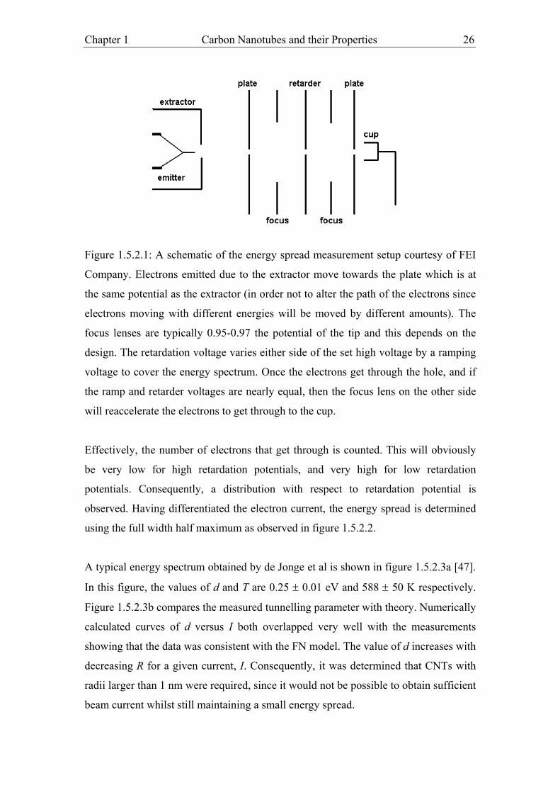
Figure 1.5.2.1: A schematic of the energy spread measurement setup courtesy of FEI
Company. Electrons emitted due to the extractor move towards the plate which is at
the same potential as the extractor (in order not to alter the path of the electrons since
electrons moving with different energies will be moved by different amounts). The
focus lenses are typically 0.95-0.97 the potential of the tip and this depends on the
design. The retardation voltage varies either side of the set high voltage by a ramping
voltage to cover the energy spectrum. Once the electrons get through the hole, and if
the ramp and retarder voltages are nearly equal, then the focus lens on the other side
will reaccelerate the electrons to get through to the cup.
Effectively, the number of electrons that get through is counted. This will obviously
be very low for high retardation potentials, and very high for low retardation
potentials. Consequently, a distribution with respect to retardation potential is
observed. Having differentiated the electron current, the energy spread is determined
using the full width half maximum as observed in figure 1.5.2.2.
A typical energy spectrum obtained by de Jonge et al is shown in figure 1.5.2.3a [47].
In this figure, the values of d and T are 0.25 ± 0.01 eV and 588 ± 50 K respectively.
Figure 1.5.2.3b compares the measured tunnelling parameter with theory. Numerically
calculated curves of d versus I both overlapped very well with the measurements
showing that the data was consistent with the FN model. The value of d increases with
decreasing R for a given current, I. Consequently, it was determined that CNTs with
radii larger than 1 nm were required, since it would not be possible to obtain sufficient
beam current whilst still maintaining a small energy spread.

27 Carbon Nanotubes as Electron Gun Sources Mark Mann
Figure 1.5.2.2: Graphs showing the relation between electron count and the full-width
half maximum (FWHM) which determines the energy spread, ΔE.
Figure 1.5.2.3: (a) Energy spectrum of a CNT recorded at 350 V and 30 nA, and fit
with the FN theory (dashed). (b) Tunnelling parameter d as function of I for two
CNTs, compared with numerically calculated curves [47]. Figure courtesy of De
Jonge et al.

Chapter 1 Carbon Nanotubes and their Properties 28
1.5.3 EMISSION STABILITY
The relationship between a material’s properties and the stability of emission for a
field emitter can be explained with the FN model of equation 1.5.1.1. Current
fluctuations have two major causes:
Variations in F
Variations in φ
Due to the exponent in equation 1.5.2.1, I is extremely sensitive to variations in F or
φ; a 1% in φ of F can change can lead to a 15% change in I. Local changes in F are
likely to occur as a result of geometric changes of the tip caused by surface migration
and ion bombardment [50]. Also, φ is sensitive to adsorbates on the surface (which is
the principle on which the ZrO Schottky emitter operates); a 25% change in φ can
lead to a two orders of magnitude change in I. Despite ultra-high vacuum operation
with a fully baked out field emitter, a layer of adsorbates forms after approximately 30
minutes followed by adsorption, vaporizing and molecular flow which can occur at
room temperature. Flashing, which is the quick heating of the emitter, is performed
regularly and operated under extremely good vacuum conditions (< 10-10 mBar) with
electronic feedback loops to stabilize the current [50]. The CNT, being a highly
crystalline covalent structure [2], does not suffer from surface migration, which is
typically observed on metal-bonded tungsten emitters, because the bond strength is
much higher. Hence, the CNT can be operated at a few hundred degrees Celsius to
continuously clean the emitter through desorption. Therefore, it was found that the
vacuum requirements for the CNT emitter could be relaxed in comparison to that
required for metal emitters.
The CNTs measured were constantly heated at 800 K during emission to avoid
contamination. The probe current, Ip, was collected in a Faraday cup which was
connected to a precision amplifier as shown in figure 1.5.3a. The extractor electrode
was grounded and the emitter biased negatively at high voltage. The current-
measuring electrode in the Faraday cup was biased positively to prevent current loss
by secondary electron emission. Figure 1.5.3b shows that the emitted current has a
29 Carbon Nanotubes as Electron Gun Sources Mark Mann
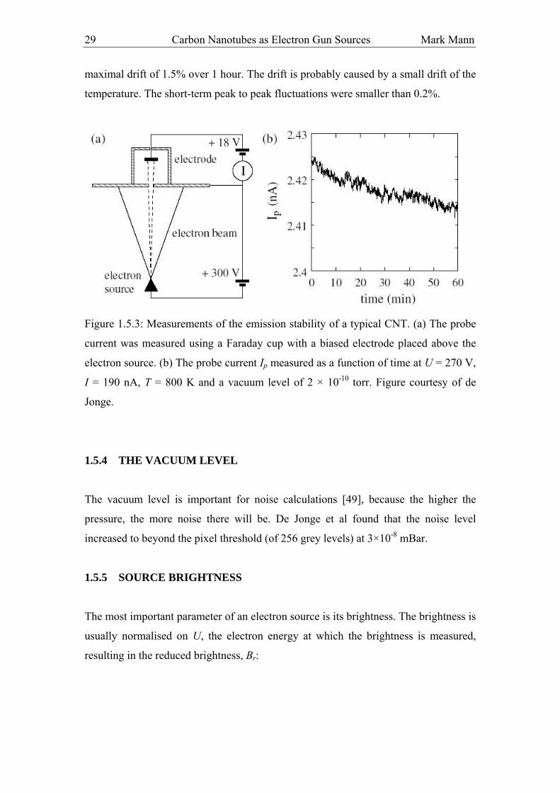
maximal drift of 1.5% over 1 hour. The drift is probably caused by a small drift of the
temperature. The short-term peak to peak fluctuations were smaller than 0.2%.
Figure 1.5.3: Measurements of the emission stability of a typical CNT. (a) The probe
current was measured using a Faraday cup with a biased electrode placed above the
electron source. (b) The probe current Ip measured as a function of time at U = 270 V,
I = 190 nA, T = 800 K and a vacuum level of 2 × 10⁻¹⁰ torr. Figure courtesy of de
Jonge.
1.5.4 THE VACUUM LEVEL
The vacuum level is important for noise calculations [49], because the higher the
pressure, the more noise there will be. De Jonge et al found that the noise level
increased to beyond the pixel threshold (of 256 grey levels) at 3×10⁻⁸ mBar.
1.5.5 SOURCE BRIGHTNESS
The most important parameter of an electron source is its brightness. The brightness is
usually normalised on U, the electron energy at which the brightness is measured,
resulting in the reduced brightness, Br:
Chapter 1 Carbon Nanotubes and their Properties 30
22
'11
v
r
vr r
IUrd
dIBππ
=Ω
= Eq. 1.5.5
with the reduced angular current density Ir´ and rv, the radius of the virtual source. For
a focusing system, the reduced brightness indicates the amount of current, which can
be focused into a spot of certain size and electron beam energy.
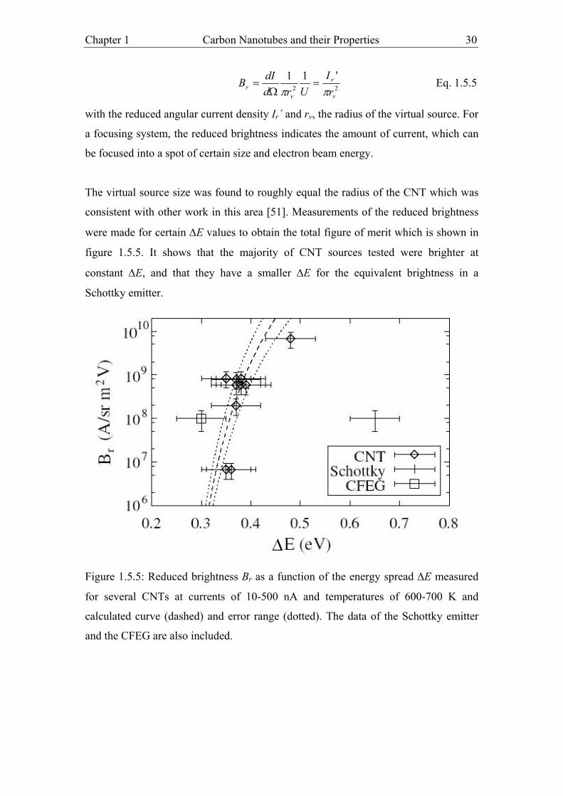
The virtual source size was found to roughly equal the radius of the CNT which was
consistent with other work in this area [51]. Measurements of the reduced brightness
were made for certain ΔE values to obtain the total figure of merit which is shown in
figure 1.5.5. It shows that the majority of CNT sources tested were brighter at
constant ΔE, and that they have a smaller ΔE for the equivalent brightness in a
Schottky emitter.
Figure 1.5.5: Reduced brightness Br as a function of the energy spread ΔE measured
for several CNTs at currents of 10-500 nA and temperatures of 600-700 K and
calculated curve (dashed) and error range (dotted). The data of the Schottky emitter
and the CFEG are also included.
31 Carbon Nanotubes as Electron Gun Sources Mark Mann
1.5.6 SOURCE LIFETIME AND FAILURE MECHANISMS
The lifetime of an individual CNT electron source can be long: many hundreds of
hours [52, 53]. For example, De Jonge et al have stated that their CNTs have lasted
over 16 months without damage at a current of 100 nA, a vacuum level of 2 × 10⁻¹⁰
mbar and at a temperature of about 800 K.
However, the range of lifetimes for CNTs is large, so whilst CNTs can last a long
time, some can fail after a few hours of field emission. The phenomena causing the
degradation of the emitters are not completely understood presently. A combination of
several factors plays a role.
Electrostatic deflection or mechanical stresses can cause alterations in the shape and
surroundings of the emitter. This can lead to a decrease in local field amplification.
High currents can also damage a nanotube rapidly. A gradual decrease in field
enhancement due to field evaporation was found in SWNTs when the emitted current
was increased beyond certain limits (ranging from 300 nA to 1 μA) [54]. For multi-
walled CNTs, a shortening of the emitter over time [55] or damage to the outer walls
of the nanotube due to high currents [56] has also been reported. Graphene layers or
caps are removed, peeled back, or the end of the tube loses its graphitic structure and
becomes amorphous [56,57]. MWNTs can be operated at total currents of up to 10
μA, but the current should be kept below 1 μA for stable operation and long life-time
[51].
Following any type of degradation, a strong decrease in the emission current is
observed and the voltage required to obtain comparable currents is substantially
higher following such an episode.
Chapter 1 Carbon Nanotubes and their Properties 32
1.6 SUMMARY
The combination of this data indicates that the CNT is a potentially powerful source
for low-voltage, high resolution electron imaging equipment and research into a
feasible fabrication method is the basis of this PhD.
Although there has been much research into field emission from carbon nanotubes,
measurements have mainly focused on the maximum current density that can be
obtained from nanotubes – research that is targeted towards field emission displays
and microwave amplifiers. The research that exists on using carbon nanotubes as field
emission sources is relatively small and focuses on carbon nanotubes attached to a tip.
Although existing data is useful in giving an indication as to how a CNT source
would behave, it does not provide data for a device that can be manufactured on a
larger scale and with reproducible characteristics. There is no data on field emission
from CNTs grown directly onto a tungsten tip, so it is of interest to see how the
characteristics of CNTs grown in this way compare to CNTs attached. For instance,
does lifetime increase? Are they easier to handle? Is alignment better? Are they
brighter, more stable, and do they have a lower or higher energy spread? These are
some of the questions that this thesis answers.
The second chapter will discuss techniques that have been employed to grow CNTs
and to manipulate them so that they can be used as field emission sources. It will also
detail various options open to the author and describe the results together with their
relative merits. The third chapter details the method settled upon which is to grow
CNTs directly onto the apex of existing tungsten electron sources and discusses yield,
reproducibility and robustness. The fourth chapter provides a detailed investigation of
the field emission characteristics of the CNT, paying particular attention to stability
and its definition, together with energy spread and brightness measurements. The fifth
chapter observes the performance of CNT electron sources in an electron microscope,
indicating their superior performance in terms of resolution, brightness and virtual
source size. The final chapter summarizes the work in this thesis and proposes where
research in this area should go in the future.

33 Carbon Nanotubes as Electron Gun Sources Mark Mann
1.7 REFERENCES
[1] S. Ijima, Nature 354, 56 (1991).
[2] Niels de Jonge and Jean-Marc Bonard, Phil. Trans. R. Soc. Lond. A 362,
2239–2266 (2004).
[3] Y. Saito, T Yoshikawa, S. Bandow, M. Tomita and T. Hayashi, Phys. Rev. B
48, 1907 (1993).
[4] M. Endo, K. Takeuchi, T. Hiraoka, T. Furuta, T. Kasai, X. Sun, C.H. Kiang,
and M.S. Dresselhaus, J. Phys. Chem. Solids 58, 1707 (1997).
[5] C.H. Kiang, M. Endo, P.M. Ajayan, G. Dresselhaus and M.S. Dresselhaus,
Phys. Rev. Lett. 81, 1869 (1998).
[6] A. Bachtold, C. Strunk, J.P. Salvelat, J.M. Bonard, L. Forro, T. Nussbaumer,
C. Schonenberger, Nature 397, 673 (1999).
[7] W. I. Milne, K. B. K. Teo, G. A. J. Amaratunga, P. Legagneux, L. Gangloff,
J.-P. Schnell, V. Semet, V. Thien Binh and O. Groening, J.Mater. Chem., 14,
1–12, 2004.
[8] H.J. Qi, K.B.K. Teo, K.K.S. Lau, M.C. Boyce, W.I. Milne, J. Robertson and
K.K. Gleason, "Determination of mechanical properties of carbon
nanotubes and vertically aligned carbon nanotube forests using
nanoindentation" Journal of Mechanics and Physics of Solids 51, 2213
(2003)
[9] J. Li, R. Stevens, L. Delzeit, H.T. Ng, A. Cassell, J. Han and M.
Meyyappan,”Electronic Properties of Multiwalled Carbon Nanotubes in an
Embedded Vertical Array", Applied Physics Letters, Vol. 81 (5), pp. 910-
912 (2002).
[10] H.J. Qi, K.B.K. Teo, K.K.S. Lau, M.C. Boyce, W.I. Milne, J. Robertson and
K.K. Gleason, "Determination of mechanical properties of carbon
nanotubes and vertically aligned carbon nanotube forests using
nanoindentation" Journal of Mechanics and Physics of Solids 51, 2213
(2003)
[11] J. Li, R. Stevens, L. Delzeit, H.T. Ng, A. Cassell, J. Han and M.
Meyyappan,”Electronic Properties of Multiwalled Carbon Nanotubes in an

Chapter 1 Carbon Nanotubes and their Properties 34
Embedded Vertical Array", Applied Physics Letters, Vol. 81 (5), pp. 910-
912 (2002).
[12] K.B.K. Teo, C. Singh, M. Chhowalla, W.I. Milne, Encyc. Nanosci.
Nanotech. X Pg 1-22, 2003.
[13] A. Bachtold, P. Hadley, T. Nakamishi, C. Dekker, Science 294, 1317 (2001).
[14] S.J. Tans, A.R.M. Verschueren, C. Dekker, Nature 393, 49 (1998).
[15] R. Martel, T. Schmidt, H.R. Shea, T. Hertel, P. Avouris, Appl. Phys. Lett.
73, 2447 (1998).
[16] V. Derycke, R. Martel, J. Appenzeller, P. Avouris, Nano. Lett. 1, 453 (2001)
[17] J. Kong, N.R. Franklin, C.W. Zhou, M.G. Chapline, S. Peng, K.J. Cho H.J.
Dai, Science 287, 6212 (2000).
[18] P.G. Collins, K. Bradley, M. Ishigami, A. Zettl, Science 287, 1801 (2000)
[19] K. Tsukagoshi, B.W. Alphenaar, H. Ago, Nature 401, 572 (1999).
[20] T.W. Tombler, C.W. Zhou, L. Alexseyev, J. Kong, H.J. Dai, L. Lei, C.S.
Jayanthi, M.J. Tang, S.Y. Wu, Nature 405, 769 (2000).
[21] R.H. Baughman, A.A. Zakhidov, W.A. de Heer, Science, 280, 1744 (1998).
[22] J. Li, R. Stevens, L. Delzeit, H.T. Ng, A. Cassell, J. Han, M. Meyyappan,
Appl. Phys. Lett. 81, 910 (2002).
[23] S. Musso, S. Porro, M. Rovere, A. Tagliaferro, E. Laurenti, M. Mann,
K.B.K. Teo, W.I. Milne. Diamond & Related Materials 15, 1085 – 1089
(2006).
[24] M. Hirscher, M. Becher, M. Haluska, U. Dettlaff-Weglikowska, A. Quintel,
G.S. Deusberg, Y.M. Choi, P. Downer, M. Hulman, S. Roth, I. Stepanek, P.
Bernier, Appl. Phys. A 72, 129 (2001).
[25] P. Calvert, nature 399, 210 (1999).
[26] Deuk-Seok Chung, S. H. Park, H. W. Lee, J. H. Choi, S. N. Cha, J. W. Kim,
J. E. Jang, K. W. Min, S. H. Cho, M. J. Yoon, J. S. Lee, C. K. Lee, J. H.
Yoo, Jong-Min Kim, J. E. Jung, Y. W. Jin, Y. J. Park, and J. B. You, Appl.
Phys. Lett. 80, 4045 (2002).

35 Carbon Nanotubes as Electron Gun Sources Mark Mann
[27] K.B.K. Teo, E. Minoux, L. Hudanski, F. Peauger, J.-P. Schnell, L. Gangloff,
P. Legagneux, D. Dieumgard, G.A.J. Amaratunga and W.I. Milne.
"Microwave Devices: Carbon Nanotubes as Cold Cathodes", Nature 437,
968 (2005).
[28] N. de Jonge, M. Allioux, J.T. Oostveen, K.B.K. Teo and W.I. Milne.
"Optical performance of carbon nanotube electron sources", Physical
Review Letters 94, 186807 (2005).
[29] W.I. Milne, K.B.K. Teo, E. Minoux, O. Groening, L. Gangloff, L. Hudanski,
J.-P. Schnell, D. Dieumegard, F. Peauger, I.Y.Y. Bu, M.S. Bell, P.
Legagneux, G. Hasko, and G.A.J. Amaratunga "Aligned carbon
nanotube/fibers for applications in vacuum microwave amplifiers", Journal
of Vacuum Science and Technology B 24, 345 (2006).
[30] Thesis K.B.K. Teo, Cambridge University, 2002.
[31] S. T. Purcell, P. Vincent, C. Journet, and Vu Thien Binh, Phys. Rev. Lett.
88, 105502 (2002).
[32] Rinzler, A. G., Hafner, J. H., Nikolaev, P., Lou, L., Kim, S. G., Tomanek,
D., Nordlander, P., Colbert, D. T. & Smalley, R. E. 1995 Unraveling
nanotubes: field emission from an atomic wire. Science 269, 1550–1553.
[33] T. Utsumi, IEEE Trans. Electron Dev. 38, 2276 (1991).
[34] Y. Wei, C. Xie, K. A. Dean, and B. F. Coll, Appl. Phys. Lett. 79, 4527
(2001).
[35] Paulmier, T., Balat-Pichelin, M., Le Queau, D., Berjoan, R. & Robert, J. F.
2001 Physicochemical behavior of carbon materials under high temperature
and ion radiation. Appl. Surf. Sci. 180, 227–245.
[36] Sources for pictures:
(a), (b): www.sidiamond.com, under ANI (Applied Nanotech Inc)
(c), (d): www.oxfordxtg.com
(e): W. B. Choi, D. S. Chung, J. H. Kang, H. Y. Kim, Y. W. Jin, I. T. Han,
Y. H. Lee, J. E. Jung, N. S. Lee, G. S. Park, and J.M. Kim, Appl. Phys. Lett
75, 3129 (1999).

Chapter 1 Carbon Nanotubes and their Properties 36
(f): Deuk-Seok Chung, S. H. Park, H. W. Lee, J. H. Choi, S. N. Cha, J. W.
Kim, J. E. Jang, K. W. Min, S. H. Cho, M. J. Yoon, J. S. Lee, C. K. Lee, J.
H. Yoo, Jong-Min Kim, J. E. Jung, Y. W. Jin, Y. J. Park, and J. B. You,
Appl. Phys. Lett. 80, 4045 (2002).
[37] Choi, W. B. (and 10 others) 1999 Fully sealed, high-brightness carbon-
nanotube field-emission display. Appl. Phys. Lett. 75, 3129–3131.
[38] Saito, Y. & Uemura, S. 2000 Field emission from carbon nanotubes and its
application to electron sources. Carbon 38, 169–182.
[39] Chung, D. S., Choi, W. B., Kang, J. H., Kim, H. Y., Han, I. T., Park, Y. S.,
Lee, Y. H., Lee, N. S., Jung, J. E. & Kim, J. M. 2000 Field emission from
4.5 in. single-walled and multiwalled carbon nanotube films. J. Vac. Sci.
Technol. B18, 1054–1058.
[40] L. Gangloff, E. Minoux, K. B. K. Teo, P. Vincent, V. T. Semet, V. T. Binh,
M. H. Yang, I. Y. Y. Bu, R. G. Lacerda, G. Pirio, J. P. Schnell, D. Pribat, D.
G. Hasko, G. A. J. Amaratunga, W. I. Milne, and P. Legagneux; Nanoletters
2004, Vol. 4, No. 9. 1575-1579.
[41] Kenneth B. K. Teo, Eric Minoux, Ludovic Hudanski, Franck Peauger, Jean-
Philippe Schnell, Laurent Gangloff, Pierre Legagneux, Dominique
Dieumegard, Gehan A. J. Amaratunga, William I. Milne; Nature Vol. 437,
2005, 968.
[42] Sugie, H., Tanemure, M., Filip, V., Iwata, K., Takahashi, K. & Okuyama, F.
2001 Carbon nanotubes as electron source in an X-ray tube. Appl. Phys.
Lett. 78, 2578–2580.
[43] Marcuccio, S., Genovese, A. & Andrenucci, M. 1997 FEEP microthruster
technology status and prospects. In Proc. 48th Int. Astronautical Federation
Cong., Turin, Italy. Paris: International Astronautical Federation.
[44] Applied Physics Technologies brochure, 1600 NE Miller St.
McMinnville, OR 97128, 2005.
[45] FEI Company brochure, 5350 NE Dawson Creek Dr.
Hillsboro, OR 97124 USA, 2005.
[46] Martijn Fransen, Towards high-brightness, monochromatic electron sources,
Technische Universiteit Delft/ Philips NatLab Promotie: 9 Februari 1999

37 Carbon Nanotubes as Electron Gun Sources Mark Mann
[47] N. de Jonge, M. Allioux, J.T. Oostveen, K.B.K. Teo and W.I. Milne.
"Optical performance of carbon nanotube electron sources", Physical
Review Letters 94, 186807 (2005).
[48] R. H. Fowler and L. Nordheim. Electron emission in intense electric fields.
Proc. Roy. Soc. London A, 119:173-181, 1928.
[49] N. de Jonge, M. Allioux, M. Doytcheva, M. Kaiser, K.B.K. Teo, R.G.
Lacerda and W.I. Milne. "Characterization of the field emission properties
of individual thin carbon nanotubes", Applied Physics Letters 85, (2004).
[50] J. F. Hainfield. Understanding and using field emission sources. Scanning
Electron Microscopy, 1:591-604, 1977.
[51] N. de Jonge. The brightness of carbon nanotube electron emitters. J. Appl.
Phys, 95:673-681, 2004.
[52] Dean, K. A. & Chalamala, B. R. 1999 The environmental stability of field
emission from single-walled carbon nanotubes. Appl. Phys. Lett. 75, 3017–
3019.
[53] Fransen, M. J., van Rooy, T. L. & Kruit, P. 1999 Field emission energy
distributions from individual multiwalled carbon nanotubes. Appl. Surf. Sci.
146, 312–327.
[54] Dean, K. A., Burgin, T. P. & Chamala, B. R. 2001 Evaporation of carbon
nanotubes during electron field emission. Appl. Phys. Lett. 79, 1873–1875.
[55] Wei, Y. Y., Dean, K. A., Coll, B. F. & Jaskie, J. E. 2001 Stability of carbon
nanotubes under electric field studied by scanning electron microscopy.
Appl. Phys. Lett. 79, 4527–4529.
[56] Wang, Z. L., Poncharal, P. & de Heer, W. A. 2002 In situ imaging of field
emission from individual carbon nanotubes and their structural damage.
Appl. Phys. Lett. 80, 856–858.
[57] Wang, Z. I., Poncharal, P. & de Heer, W. A. 2000 Nanomeasurements in
transmission electron microscopy. Microsc. Microanalysis 6, 224–230.
Related Documents