Materials 2010, 3, 2834-2883; doi:10.3390/ma3042834 materials ISSN 1996-1944 www.mdpi.com/journal/materials Review Luminescence in Sulfides: A Rich History and a Bright Future Philippe F. Smet 1, *, Iwan Moreels 2 , Zeger Hens 2 and Dirk Poelman 1 1 LumiLab, Department of Solid State Sciences, Ghent University, Krijgslaan 281-S1, Gent, Belgium; E-Mail: [email protected] (D.P.) 2 Physics and Chemistry of Nanostructures, Department of Physical and Inorganic Chemistry, Ghent University, Krijgslaan 281-S3, Gent, Belgium; E-Mails: [email protected] (I.M.); [email protected] (Z.H.) * Author to whom correspondence should be addressed; E-Mail: [email protected]; Tel.: +32-9-264-4353; Fax: +32-9-264-4996. Received: 8 April 2010 / Accepted: 18 April 2010 / Published: 21 April 2010 Abstract: Sulfide-based luminescent materials have attracted a lot of attention for a wide range of photo-, cathodo- and electroluminescent applications. Upon doping with Ce 3+ and Eu 2+ , the luminescence can be varied over the entire visible region by appropriately choosing the composition of the sulfide host. Main application areas are flat panel displays based on thin film electroluminescence, field emission displays and ZnS-based powder electroluminescence for backlights. For these applications, special attention is given to BaAl 2 S 4 :Eu, ZnS:Mn and ZnS:Cu. Recently, sulfide materials have regained interest due to their ability (in contrast to oxide materials) to provide a broad band, Eu 2+ -based red emission for use as a color conversion material in white-light emitting diodes (LEDs). The potential application of rare-earth doped binary alkaline-earth sulfides, like CaS and SrS, thiogallates, thioaluminates and thiosilicates as conversion phosphors is discussed. Finally, this review concludes with the size-dependent luminescence in intrinsic colloidal quantum dots like PbS and CdS, and with the luminescence in doped nanoparticles. Keywords: sulfides; photoluminescence; electroluminescence; phosphor; rare earth; nanocrystals; quantum dots; europium; cerium; light emitting diodes; persistent luminescence; storage phosphor OPEN ACCESS

Welcome message from author
This document is posted to help you gain knowledge. Please leave a comment to let me know what you think about it! Share it to your friends and learn new things together.
Transcript

Materials 2010, 3, 2834-2883; doi:10.3390/ma3042834
materials ISSN 1996-1944
www.mdpi.com/journal/materials
Review
Luminescence in Sulfides: A Rich History and a Bright Future
Philippe F. Smet 1,*, Iwan Moreels 2, Zeger Hens 2 and Dirk Poelman 1
1 LumiLab, Department of Solid State Sciences, Ghent University, Krijgslaan 281-S1, Gent,
Belgium; E-Mail: [email protected] (D.P.) 2 Physics and Chemistry of Nanostructures, Department of Physical and Inorganic Chemistry, Ghent
University, Krijgslaan 281-S3, Gent, Belgium; E-Mails: [email protected] (I.M.);
[email protected] (Z.H.)
* Author to whom correspondence should be addressed; E-Mail: [email protected];
Tel.: +32-9-264-4353; Fax: +32-9-264-4996.
Received: 8 April 2010 / Accepted: 18 April 2010 / Published: 21 April 2010
Abstract: Sulfide-based luminescent materials have attracted a lot of attention for a wide
range of photo-, cathodo- and electroluminescent applications. Upon doping with Ce3+
and
Eu2+
, the luminescence can be varied over the entire visible region by appropriately
choosing the composition of the sulfide host. Main application areas are flat panel displays
based on thin film electroluminescence, field emission displays and ZnS-based powder
electroluminescence for backlights. For these applications, special attention is given to
BaAl2S4:Eu, ZnS:Mn and ZnS:Cu. Recently, sulfide materials have regained interest due to
their ability (in contrast to oxide materials) to provide a broad band, Eu2+
-based red
emission for use as a color conversion material in white-light emitting diodes (LEDs). The
potential application of rare-earth doped binary alkaline-earth sulfides, like CaS and SrS,
thiogallates, thioaluminates and thiosilicates as conversion phosphors is discussed. Finally,
this review concludes with the size-dependent luminescence in intrinsic colloidal quantum
dots like PbS and CdS, and with the luminescence in doped nanoparticles.
Keywords: sulfides; photoluminescence; electroluminescence; phosphor; rare earth;
nanocrystals; quantum dots; europium; cerium; light emitting diodes; persistent
luminescence; storage phosphor
OPEN ACCESS

Materials 2010, 3
2835
In this Review, we discuss the rich and longstanding history of sulfide phosphor materials, dating
back from at least the 17th century. Progress in the understanding of the basic principles of
luminescence culminated in several typical applications, uniquely based on sulfides, such as ZnS-
based powder electroluminescence and thin film electroluminescence. Turning towards the 21st
century, sulfide-based nanoparticles and color conversion phosphors possess several characteristic
properties which give them a bright future as well.
The paper is structured as follows:
1. Sulfide phosphors: A short history
2. Electroluminescent powders
3. Lamp and CRT phosphors
4. Thin film electroluminescence
5. Color conversion phosphors
6. Persistent and storage phosphors
7. Luminescent sulfide nanoparticles
8. Conclusions
1. Sulfide phosphors: A Short History
Luminescent phenomena have fascinated mankind since the earliest times. The light from the aurora
borealis, glow worms, luminescent wood, rotting fish and meat are all examples of naturally occurring
luminescence. The effect was shrouded in mystery, and described accordingly in the Middle Ages and
beyond. The earliest written account of a solid state luminescent material comes from a Chinese text
published in the Song dynasty (960–1279 A.D.), referring to a book (never recovered) from the period
140-88 B.C. It describes a painting of a cow grazing outside. In the dark, the cow would have been
seen resting inside a barn [1,2]. Possibly, the ink used was the first man-made persistent phosphor
material. Harvey [3] presents an excellent account of these early observations far beyond the scope of
the present review.
The first artificial phosphor described in Western literature dates from 1603. Then, the Italian
shoemaker and alchemist Vincenzo Cascariolo used the natural mineral barite (BaSO4), found near
Bologna, in an effort to create gold. After heating the ground stone under reducing condition he–
obviously – did not obtain gold, but a persistent luminescent material. This so-called Bolognian stone
became famous and a subject of study and admiration for decades to come [3]. It is not clear which
dopant or dopants were actually responsible for the persistent luminescence, but the host material [2]
definitely was BaS. While not made intentionally but by serendipity, BaS thus is the first sulfide
phosphor ever synthesized. The name phosphor (from the Greek „light bearer‟) was already used at
that time, even if the chemical element phosphorous was only isolated in 1669 (from urine) by the
German alchemist Hennig Brand [1]. Phosphorous becomes luminescent under moist conditions, when
it oxidizes. Thus, phosphorous is chemiluminescent and the name phosphorescence for persistent
„glow in the dark‟ photoluminescence is actually a bit of a misnomer [4].
In the following centuries, many scientists synthesized and investigated luminescent materials, but
it was too early for a systematic study. However, the synthesis of CaS as a phosphor in 1700 by
Friedrich Hoffmann and of SrS in 1817 by J. F. John are worth mentioning. Curiously enough, the
Materials 2010, 3
2836
luminescent properties of ZnS, which was going to become one of the most important luminescent
hosts in the 20th century, were not recognized until 1866, when the so-called Sidot blend (hexagonal
ZnS) was developed by Theodor Sidot [5]. In 1888, Eilhard Wiedemann was the first to classify
different classes of phosphors according to the type of excitation, and is credited for introducing the
terms luminescence, photoluminescence, electroluminescence, thermoluminescence,
crystalloluminescence, triboluminescence and chemiluminescence [6].
2. Electroluminescent Powders
Already in 1907, H. J. Round published light emission from a silicon carbide junction diode, the
first light emitting diode (LED) ever. Independently, Losev observed emission from ZnO and SiC
diodes, as published in 1927 [7]. However, as LED‟s are injection electroluminescent devices and
contain no phosphors, we will not deal with this kind of devices further on.
Destriau is credited for the discovery of phosphor-based high field electroluminescence in solids in
1936 [8]. The original Destriau cell consisted of a Cu-doped ZnS powder in castor oil, insulated from
one of the electrodes by a mica sheet. The applied AC voltage was very high and the light emission
very poor, leading to the suspicion that the actual light emission was not due to electroluminescence by
excitation of the ZnS:Cu, but due to the photoluminescence of the ZnS:Cu, excited by the UV emission
of electrical discharges in gases in the porous powders [4,9]. In the following years, planar
electroluminescent devices were developed, helped by the availability of SnO2 as a transparent
conductor. EL panels were incorporated for dashboard back illumination from the late 1950‟s, for
example in the Chrysler Imperial 1960 luxury car. In an effort to reduce the size and energy
consumption of displays, 7 segment electroluminescent numerical displays were used in the Apollo
program DSKY (display panel and keyboard) module instead of the traditional nixie tubes. Quite
luckily for the developers of EL devices, the repeated failures of a segment of this display during the
Apollo 11 mission were later attributed to a faulty driving circuit [10] and not to problems with the
display itself.
Many research groups were active in the research on powder EL, but especially the contributions by
Thornton [11], Piper and Williams [12], and Vecht [13] should be noted. The research on powder EL
has been marked by periods of intense research and success followed by periods of disillusion and
discouragement. At the beginning and the middle of the 1960s, a series of books and book chapters
gathered the – now largely forgotten – knowledge accumulated during the former phase [14-21].
AC powder electroluminescent devices (ACPEL devices in short) typically consist of a doped ZnS
powder suspended in a dielectric binder, sandwiched between electrodes and supported on a substrate.
The substrate can be metallic or insulating (glass or plastic). An additional white reflecting layer could
provide additional electric protection and improved light output from the device.
Similar DCPEL devices require a highly conductive surface layer for current injection into the
phosphor particles. Devices are prepared using Cu concentrations higher than the solubility limit in
ZnS. While the surface excess Cu is washed away in the case of ACPEL devices, it is converted into
an inhomogeneous conductive layer using an electrically-assisted forming process. Several models
have been proposed on the exact mechanism of this process, but there is evidence of the formation of
needle-like Cu2-xS phases. As Cu2-xS is p-type and ZnS is weakly n-type, this could lead to an

Materials 2010, 3
2837
improved carrier injection in the ZnS particles. In addition, DCPEL phosphors require a very
monodisperse and small particle size in order to limit current inhomogeneity and electric breakdown.
Copper is thus essential in all DCPEL devices, acting both for current injection and as a light emitting
dopant. Next to copper, manganese has been used extensively as a dopant in both AC and DC powder
EL devices, improving brightness and increasing the possible color gamut.
DCPEL panels are – in principle – ideally suited for graphical displays. A few commercial
applications have emerged, which are now superseded by other display technologies. There is very
little recent research interest in DCEL. A detailed review on DCEL devices was written by Chadha [9].
AC powder electroluminescent devices are still used in the niche application of very thin, low light
level, low cost, large area background lights on flexible substrates, such as electronic gadgets, cell
phones, remote controls and car radios. A number of issues prevent their widespread use:
The absolute brightness is quite low. As large areas can emit quite homogeneously, the total light
output can be considerable, but making a sunlight readable device, requiring high surface brightness,
is a problem.
The lifetime of moderate to high luminance devices is limited. The brightness of an ACPEL device
can be increased by increasing the applied voltage, but this in turn decreases the lifetime. Thus a
low luminance device can last for many 1000s of hours, but this lifetime decreases drastically at
increased luminance. With improvements in technology, a lifetime of about 2500 h (at 50% relative
luminance) with an initial luminance of 100 cd/m2 can now be achieved [22]. Probably, the
degradation is related to diffusion of copper or blunting of the copper needles in the phosphor layer,
but this is still a matter of debate. Chen et al. showed that the degradation rate increases at higher
operating temperatures and almost drops to zero when operated at -67 °C, suggesting diffusion
related degradation [23]. Heating of degraded devices to 200 °C leads to a partial rejuvenation [24].
The stability, and thus the lifetime, is highly dependent on the encapsulation of the layers. As these
are moisture sensitive, they should be very well shielded from the ambient. First, the layers were
encapsulated as a whole, but more recently, micro-encapsulation has been performed, the particles
being coated individually. Obviously, this kind of additional process increases the cost of the
material.
The overall external efficiency of ACPEL devices is very low, of the order of only a few lm/W,
which makes the technology unsuited for general lighting applications, and certainly not a match
for CFL‟s (compact fluorescent lamps) and LEDs.
As ZnS:Cu is the only material for efficient powder EL, there seems little room for drastic
improvements in device performance. At best, powder EL will remain a technology for blue-green –
the emission color being frequency dependent - background lighting for undemanding applications. A
recent review on ACPEL can be found here [25].
3. Lamp and CRT Phosphors
Starting before the Second World War, many new luminescent materials were developed for
fluorescent lighting. In a fluorescent lamp, the ultraviolet emission of an electrical discharge of a low
pressure mercury vapor is converted to visible light by phosphor materials, covering the inside of the

Materials 2010, 3
2838
lamp. Sulfide phosphors are of no use in this kind of fluorescent lamps, since they react with
mercury [26].
Since the advent of high performance flat panel displays a few years ago, any treatment of CRT
(cathode ray tube) phosphors is – almost by definition – of historical interest. After its discovery by
Braun in 1897, the CRT has had tremendous success. One of the first CRT images (the Japanese
Katakana character “i”) was shown in 1926 by Takayanagi. First screens were black and white, later
full color displays were taken into production, thanks to the development of a large number of highly
optimized possible phosphor materials [2,26]. For blue cathodoluminescence, ZnS:Ag has been the
material of preference since the beginning. It has a very efficient emission due to a donor acceptor
transition: the donor level being due to an aluminum or chlorine co-dopant and the acceptor level due
to silver [26]. This kind of process implies that the emission wavelength is not determined by the
nature of the dopants, but by the band gap of the host. By making a solid solution of ZnS and CdS, the
spectrum of Zn1-xCdxS:Ag could be tuned from a peak wavelength of 450 to 620 nm [4]. Thus, both
green and red emitting phosphors could be made using this technique. Nowadays, such Cd-containing
compounds have become unacceptable for environmental reasons. For the green phosphor, ZnS:Cu
(codoped with Al or Cl) is routinely used. For the red one, the line emission from Eu3+
was found to be
an ideal compromise between optimum color coordinates and eye sensitivity [26]. The host of choice
for red emission is Y2O2S. Many other cathodoluminescent phosphors were developed for specific
applications, like projection displays (high excitation current), field emission displays (FED) (low
voltage, high current) and flying spot equipment (fast decay times). Their study and description is
outside the scope of this review. A recently compiled list of CRT and FED phosphors can be found
here [27,28].
4. Thin Film Electroluminescence
4.1. Working principle
In parallel with the development of powder EL, a new type of device, using a thin film phosphor,
was presented by Vlasenko and Popkov in 1960 [29]. The device used ZnS:Mn as the active layer and
was much brighter than an equivalent powder EL lamp. However, stability was a problem due to the
very high electric fields, needed to drive the device. This problem was largely solved by Russ and
Kennedy in 1967, who proposed a double-insulated structure, protecting the active layer from
destructive dielectric breakdown [30]. The resulting device structure, which is still used to date, is
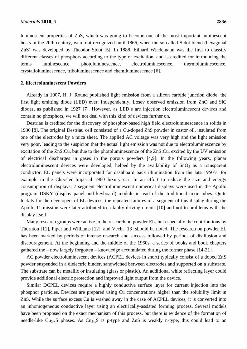
shown schematically in Figure 1.
When a voltage is applied over the electrodes, it is capacitively divided between the two insulators
and the central active layer. As both insulating layers and active layer have a large band gap, there are
a negligible number of free electrons and holes available and no current is flowing. However, there are
a number of allowed energy levels at the insulator-active layer interfaces (appropriately called
interface states). To a certain extent, these are filled with electrons. When the electric field is high
enough, of the order of 1 – 2.108 V/m, the energy bands are tilted and Fowler-Nordheim tunneling of
the electrons at the cathodic interface into the conduction band of the active layer becomes possible.
These electrons are then accelerated to high energies by the high electric field, and can impact/excite
the activator ions in the central layer. When the activator ion returns into the ground state, light is
Materials 2010, 3
2839
emitted. The active layer thus acts as a „leaky‟ capacitor in these high fields, and electrons are
transported from the cathodic to the anodic insulator-active layer interface. This charge transfer creates
an additional electric field opposite to the applied field, therefore the tunneling, charge transfer and
light emission stop after some time, usually after some microseconds. Quasi continuous light emission
is obtained by AC driving of the device: a short light pulse is emitted at each polarity switch of the
applied voltage. A much more detailed discussion of the physics of these ACTFEL (AC thin film
electroluminescent) devices was given by Mach and Mueller [31-33] and Rack and Holloway [34].
Figure 1. M(etal)-I(nsulator)-S(emiconductor)-I(nsulator)-M(etal) structure used for thin
film electroluminescence displays (color online).
Curiously enough, it lasted until 1974 before an ACTFEL display using the device structure of Russ
and Kennedy was presented [35]. In the following years, several companies started producing
monochrome orange emitting displays based on ZnS:Mn, some of which are still being made. While
this kind of display cannot offer the visual performance and display size of other modern flat panel
display technologies, it does serve a niche market where its unique properties are needed:
ACTFEL displays can have an unsurpassed lifetime of the order of 50.000 hours.
As this is a fully solid state display, it can be made very rugged to withstand harsh environments, in
industrial, medical, military or aviation applications.
The tunneling mechanism, which is the cornerstone of the device operation, is essentially
independent of temperature. Therefore, these displays can be made to work at extremely low and
high temperatures, the temperature range of the drive electronics being the main limiting factor. An
EL device has been reported to work down to 15 K [36].
ACTFEL is an emissive display technology; therefore, the viewing angle can be very large, of the
order of 170°, both horizontally and vertically.
If transparent conductors are used for both top and bottom electrodes in Figure 1, the entire display
can be made transparent [37].
The active layer is very thin – of the order of 500 nm – therefore the display resolution can be high.
A microdisplay with a pixel pitch of 24 µm was presented by Planar Systems [38].

Materials 2010, 3
2840
The main drawback of ZnS:Mn ACTFEL displays was the lack of full color capability. Multicolor
displays can be made by filtering the wide orange wavelength distribution of the ZnS:Mn emission to
green and red [39], but RGB full color is impossible (Figure 2).
Figure 2. Emission spectrum of (a) BaAl2S4:Eu [40], (b) SrS:Ce,Cl and (c) ZnS:Mn [41].
4.2. Towards full-color EL
In a first effort to obtain different emission colors, the Mn dopant in ZnS was replaced by trivalent
rare earth luminescent centers [42-44], notably Tb, Er, Dy, Sm, Nd, Tm, Ho and Pr. The emission from
these ions is due to well shielded 4f-4f transitions, giving rise to sharp emission peaks. As the size of
the trivalent rare earth ions typically is much larger than that of the Zn cation in ZnS, it is not easy to
incorporate these ions substitutionally, although higher dopant concentrations can be obtained in thin
films compared to single crystals or bulk powders. For most of the rare earth ions, a rather weak
emission was observed. Only ZnS:Tb (efficient green emission) [45,46], ZnS:Sm (weak red emission)
[47] and ZnS:Ho (white) [48] have received some interest in later years. For ZnS:Tb, the efficiency
was increased by codoping with fluorine [42] and it was shown that actually TbOF centers were
formed [49], thus conserving charge neutrality.
Alternative hosts for luminescent dopants were found by returning to the well known sulfide
phosphors from the 19th century. Indeed, the basic requirements for the active layer in an ACTFEL
device are [50-52]:
A wide band gap semiconductor is needed, as it has to be transparent to the emitted light. However,
the band gap should not be too high, allowing avalanche multiplication processes.
The dopant chosen should show an efficient emission under high electric fields, which excludes
donor-acceptor based emission. Therefore ions with internal transitions are preferred, such as
encountered in Mn2+
and the rare earth ions (both 4f-4f and 5d-4f emittors).
The host‟s cation size should match the size of the dopant ions to facilitate the substitutional
incorporation in the host lattice. In addition, its oxidation state should preferably be the same as that
of the dopant, although charge compensating co-dopants can be used. The ideal concentration of the
dopants depends on the type of dopant, but is typically in the order of 1%. At higher concentration,
Materials 2010, 3
2841
non-radiative decay becomes more important because of an increased energy transfer between
dopant ions. Also, high dopant concentrations can distort the host lattice thus lowering the
excitation efficiency. This will especially be important for dopant ions with deviating valence state
and/or ionic radius compared to the substituted ion.
A very important parameter, which precludes the use of almost all oxides, is the need for a
crystalline layer. In the applied electric field, electrons should be accelerated ballistically [53]. If
the layer is amorphous, electrons are scattered at numerous grain boundaries and thus cannot gain
sufficient energy to impact/excite the activator ions. While sulfides quite easily crystallize at
moderate temperatures (around 500 °C), very high processing temperatures are typically needed for
crystallizing oxide materials. Another effect favors the use of sulfide materials. At high electric
fields (in the order of MV/cm), electron-phonon interaction is the main scattering mechanism.
Hence, host compounds having low optical-phonon energies are favored. Benalloul et al. compared
phonon energies of sulfides and oxides and observed significantly lower values for sulfides
compared to oxides [54]. The optical-phonon energy for ZnS (44meV) is similar to the one in
BaAl2S4 (30-40meV) [55], both being efficient EL hosts.
In the middle of the 1980s it became clear that rare earth doping of ZnS would not lead to
sufficiently bright EL materials. As a result, several new activator-host combinations were tested and
found to yield bright emission, CaS:Ce (green) [56], SrS:Ce (blue-green) [57], CaS:Eu (red) [58] and
SrS:Eu (orange) [59] being the most successful combinations. In these phosphors, the luminescent ions
are Eu2+
and Ce3+
. Within the range of rare earth ions, they are exceptional in the sense that the
luminescent electronic transition is due to a 5d – 4f transition, which is not well shielded from the
crystal field of the host lattice. This has two effects: first of all, the emission has a broadband spectrum
and secondly, the emission spectrum can be influenced by changing the host. Since several of the
sulfides form solid solutions in all compositions, without any phase change, it became possible to tune
the color coordinates of the emission by changing the ratio of the components in the solid solution.
This fact was employed successfully in Ca1-xSrxS:Eu (orange to red) [60,61], CaS1-xSex:Eu (orange to
red) [62,63] and SrS1-xSex:Ce (blue to blue-green) [64-66]. The research on the latter two hosts was,
however, abandoned due to the high toxicity of H2Se [67], which is liberated upon exposure of the
material to moisture.
The subsequent research into improving material quality led to a prototype of a full color computer
monitor type display by Planar in 1993 [68]. The way in which this display was constructed, shows the
state of the art and the remaining problems at that time: The red and green pixels of the display used
filtered ZnS:Mn emission, and the blue phosphor was filtered SrS:Ce. A major drawback of SrS:Ce for
display applications is indeed the broad emission spectrum from Ce3+
: the effective emission spectrum
is blue-green, and the green component has to be filtered out to obtain saturated blue (Figure 2). In the
prototype display in 1993, not only the size of the SrS:Ce pixels was larger than that of the ZnS:Mn
pixels, but also the drive frequency of the SrS:Ce pixels was higher, both tricks meant to obtain a
sufficiently intense blue emission.
In the following years, most research on ACTFEL phosphors was devoted to improving the
intensity, color purity and stability of the blue component. As most sulfide phosphors are hygroscopic
[69], reactions with the ambient and with the insulating layers had to be prevented. Secondly, due to
Materials 2010, 3
2842
the low sticking coefficient of sulfur, films prepared by PVD (physical vapor deposition) methods
were sulfur deficient. This fact was usually overcome by co-evaporation of sulfur or reactive
deposition in an H2S atmosphere. Thirdly, films deposited at low temperature by PVD processes were
amorphous. In order to obtain polycrystalline layers, high substrate temperatures or post-deposition
annealing treatments [70] had to be used. Finally, while the most straightforward PVD technique for
sulfide films is electron beam evaporation, alternative techniques such as magnetron sputtering [71]
and ALD (atomic layer deposition) [72,73] were also employed, allowing a better control of the thin
film properties.
In the early 1990s, when it was realized that the (filtered) blue emission intensity in SrS:Ce
remained low, research efforts were directed towards ternary sulfide hosts. The ternary thiogallates
CaGa2S4 and SrGa2S4 were proposed as a new class of promising TFEL phosphors, doped with Ce or
Eu [74,75]. However, these materials did not provide a real breakthrough of ACTFEL technology due
to the difficulty to prepare high quality thin films that allowed sufficient electron acceleration.
In 1997, SrS:Cu and SrS:Cu,Ag were investigated for the first time as blue-emitting ACTFEL-
phosphors [36,66,76,77]. In contrast to the situation of Cu as a dopant in ZnS, where a donor-acceptor
transition is taking place, the emission was found to result from an internal transition of the Cu-ion.
Unfortunately, the luminescence in SrS:Cu,(Ag) suffered from severe thermal quenching and
dependence of the emission spectrum on the exact preparation conditions of the phosphors [66].
Indeed, in the years following 1997, several papers on the same material were published, consistently
showing entirely different results.
Also in the 1990s, CaS:Pb was briefly considered as one of the best candidates for blue thin film EL
[73,81-84]. Problems with clustering of the Pb ions, leading to a red shift of the emission and problems
with crystallinity, prevented this phosphor becoming popular. CaS:Bi, a phosphor which had been
marketed already in 1870 as Balmain‟s paint, the first well-recognized commercial luminescent
pigment [3], was also tested, but revealed similar problems as CaS:Pb [85].
1999 turned out to be a very important year for ACTFEL as the new blue phosphor BaAl2S4:Eu was
presented by N. Miura from Meiji University, Japan [86,87], with properties that were far superior to
any previously investigated material. As this is a phosphor of current interest, it will be treated in more
detail in the following paragraphs. The most important thin film EL phosphors studied in the 20th
century are listed in Table 1.

Materials 2010, 3
2843
Table 1. Overview of proposed thin film electroluminescent materials with their emission
color and dominant wavelength (d).
Material Color d (nm) Refs.
ZnS:Mn Amber 585 [29]
ZnS:Tb Green 545 [46,78,79]
ZnS:Ho White 550 [44,48]
ZnS:Sm Red 651 [47]
CaS:Ce Green 505 [56]
SrS:Ce Blue-green 480 [57]
CaS:Eu Red 660 [58]
SrS:Eu Orange 610 [59]
SrS1-xSex:Ce Blue 465 [64]
CaS1-xSex:Eu Orange-red 630 [62,63,80]
CaSr1-xSx:Eu Orange-red 640 [61]
CaS:Pb Blue 450 [73,81-84]
CaS:Bi Blue 450 [85]
BaAl2S4:Eu Blue 475 [86-89]
CaGa2S4:Ce Blue 460 [90]
CaGa2S4:Eu Yellow 565 [91]
SrGa2S4:Ce Blue 445 [90,92-94]
SrGa2S4:Eu Green 532 [71,75,94,95]
SrS:Cu Blue-green 480 [36,77]
SrS:Cu,Ag Blue 440 [36,76,77]
CaS:Cu,Ag Blue 450 [96]
4.3. BaAl2S4:Eu and color-by-blue
The research into SrGa2S4:Ce as blue emitting phosphor was followed by the introduction of
BaAl2S4:Eu as an efficient blue emitter, with a relatively narrow emission band centered around
470 nm [97]. Although briefly mentioned by Benalloul et al. in 1998 as a promising but difficult to
synthesize material in thin film form [54], the breakthrough came in 1999 with the announcement by
Miura et al. of „High-luminance blue-emitting BaAl2S4:Eu thin film electroluminescent devices‟ [86].

Materials 2010, 3
2844
4.3.1. Deposition techniques
Using a dual-source pulsed e-beam evaporation of BaS:Eu and Al2S3, followed by a thermal
annealing at 900 °C in argon, a luminance of 65 cd/m² at 50 Hz was obtained at approximately 80 V
above threshold. With CIE color coordinates of (0.12, 0.10), this phosphor was close to the
requirements for the blue component in television displays. The dual-source pulsed evaporation is
based on the electron beam being rapidly switched (duty cycle of 10 ms) between both sources
(Figure 3), with the evaporation rate of both materials and thus the stoichiometry being determined by
the electron flux ratio to both sources, which is considerably more reproducible and reliable than using
thickness monitors [98].
This dual-source technique overcomes the non-stoichiometric evaporation when trying to evaporate
BaAl2S4:Eu powder directly by an electron-beam. To improve the compositional and thickness
homogeneity of the deposited thin films over large areas, substrates were mounted on a rotating dome
with specific positioning of two BaS:Eu and two Al2S3 sources (Figure 3). In this way, five 17‟‟
displays could be simultaneously covered [98].
Figure 3. (left) Dual source electron beam deposition for BaAl2S4:Eu thin films, (middle) evaporation of both sources is obtained by rapidly switching the single electron beam (with
constant current). Stoichiometry is achieved by tuning the time ratio between both sources,
(right) multi-source modification for improved stoichiometry over large areas. (adapted
from [86,104]).
Initially, high annealing temperatures were required to obtain devices with high luminance
(typically 900 °C), putting severe constraints on the substrate and the bottom electrodes and insulators.
An increase of the substrate temperature from 150 °C [86] to 650 °C [99] was proposed to lower or
eliminate the need for post-deposition annealing. Furthermore, a modified BaAl2S4:Eu phosphor with a
partial substitution of Ba by Mg also eased the temperature requirements [100], as well as the using of
fluxing agents, such as fluorides [101].
Based on research on BaAl2S4(:Eu) powders and thin films [89,102], a second crystallographic
phase was identified besides the well-known, cubic phase which is obtained at high temperatures
Materials 2010, 3
2845
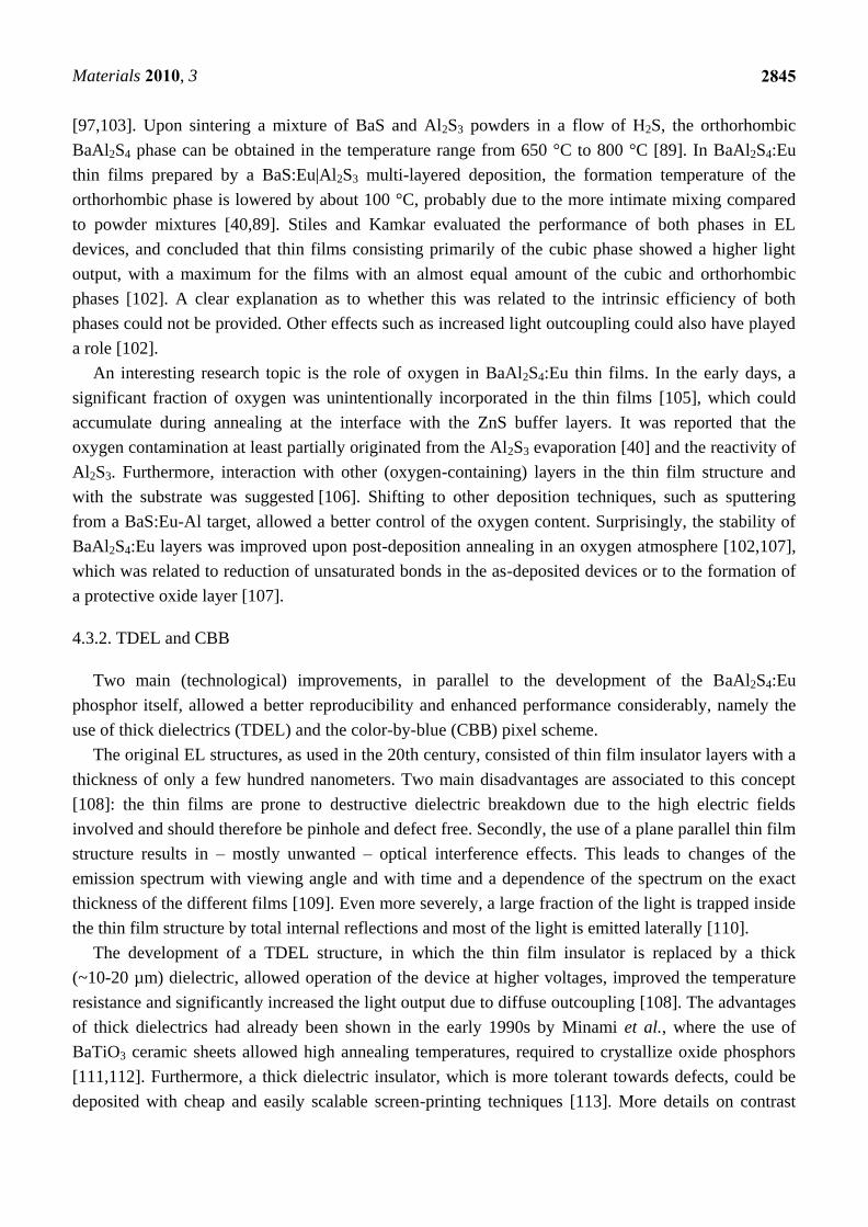
[97,103]. Upon sintering a mixture of BaS and Al2S3 powders in a flow of H2S, the orthorhombic
BaAl2S4 phase can be obtained in the temperature range from 650 °C to 800 °C [89]. In BaAl2S4:Eu
thin films prepared by a BaS:Eu|Al2S3 multi-layered deposition, the formation temperature of the
orthorhombic phase is lowered by about 100 °C, probably due to the more intimate mixing compared
to powder mixtures [40,89]. Stiles and Kamkar evaluated the performance of both phases in EL
devices, and concluded that thin films consisting primarily of the cubic phase showed a higher light
output, with a maximum for the films with an almost equal amount of the cubic and orthorhombic
phases [102]. A clear explanation as to whether this was related to the intrinsic efficiency of both
phases could not be provided. Other effects such as increased light outcoupling could also have played
a role [102].
An interesting research topic is the role of oxygen in BaAl2S4:Eu thin films. In the early days, a
significant fraction of oxygen was unintentionally incorporated in the thin films [105], which could
accumulate during annealing at the interface with the ZnS buffer layers. It was reported that the
oxygen contamination at least partially originated from the Al2S3 evaporation [40] and the reactivity of
Al2S3. Furthermore, interaction with other (oxygen-containing) layers in the thin film structure and
with the substrate was suggested [106]. Shifting to other deposition techniques, such as sputtering
from a BaS:Eu-Al target, allowed a better control of the oxygen content. Surprisingly, the stability of
BaAl2S4:Eu layers was improved upon post-deposition annealing in an oxygen atmosphere [102,107],
which was related to reduction of unsaturated bonds in the as-deposited devices or to the formation of
a protective oxide layer [107].
4.3.2. TDEL and CBB
Two main (technological) improvements, in parallel to the development of the BaAl2S4:Eu
phosphor itself, allowed a better reproducibility and enhanced performance considerably, namely the
use of thick dielectrics (TDEL) and the color-by-blue (CBB) pixel scheme.
The original EL structures, as used in the 20th century, consisted of thin film insulator layers with a
thickness of only a few hundred nanometers. Two main disadvantages are associated to this concept
[108]: the thin films are prone to destructive dielectric breakdown due to the high electric fields
involved and should therefore be pinhole and defect free. Secondly, the use of a plane parallel thin film
structure results in – mostly unwanted – optical interference effects. This leads to changes of the
emission spectrum with viewing angle and with time and a dependence of the spectrum on the exact
thickness of the different films [109]. Even more severely, a large fraction of the light is trapped inside
the thin film structure by total internal reflections and most of the light is emitted laterally [110].
The development of a TDEL structure, in which the thin film insulator is replaced by a thick
(~10-20 µm) dielectric, allowed operation of the device at higher voltages, improved the temperature
resistance and significantly increased the light output due to diffuse outcoupling [108]. The advantages
of thick dielectrics had already been shown in the early 1990s by Minami et al., where the use of
BaTiO3 ceramic sheets allowed high annealing temperatures, required to crystallize oxide phosphors
[111,112]. Furthermore, a thick dielectric insulator, which is more tolerant towards defects, could be
deposited with cheap and easily scalable screen-printing techniques [113]. More details on contrast

Materials 2010, 3
2846
enhancement (to counteract the reduced contrast due to the increased diffuse outcoupling) can be
found in the review of (TD)EL technology by Heikenfeld and Steckl [108].
The performance of BaAl2S4:Eu as a blue phosphor for EL, in combination with the TDEL
approach, turned out to be so good that a new device structure, based on only one emitting material,
could be introduced. Instead of using two or three different electroluminescent phosphor materials for
the production of full-color EL displays, a color-by-blue (CBB) approach was developed [102,113]. In
this way all three (RGB) sub-pixels are based on the EL emission in BaAl2S4:Eu, with
photoluminescent layers (outside the electrically active structure) converting the blue emission to red
and green (Figure 4). This down-conversion concept was already shown in the 1990‟s by using an UV-
emitting EL phosphor (ZnF2:Gd) in combination with one or more photoluminescent materials
[114-116]. The CBB concept eliminates the effects of color shifts caused by differential ageing of
different EL phosphor materials during the lifetime of the device. Furthermore, no subsequent
patterning and deposition of the phosphor layers is required [102]. On top of the non-converted
subpixels, a color correcting filter can be deposited to improve the color saturation [108]. To reduce
the color blur, caused by the excitation of the conversion material by light from neighboring blue
subpixels, screen-printing black stripes in between the subpixels was proposed [117]. It is interesting
to compare the CBB approach to earlier attempts to use a color-by-white approach (Figure 4) [50]. In
this case, a single white phosphor [118] or a stack of multi-color phosphors [119] is used to produce
white light emission for every sub-pixel. Then color filters are used to filter out saturated R, G and B
colors. This has the advantage, compared to an RGB-phosphor approach, that no consecutive etching
and deposition of the phosphor layer is required. A disadvantage is a relatively large loss in efficiency
by filtering, which occurs for all sub-pixels. In CBB, the advantage of a single emissive material for all
sub-pixels is combined with high efficiency, apart from the (Stokes) conversion losses in the G and R
sub-pixels.
Figure 4. Pixel layout for thin film electroluminescence displays, with RGB subpixels
(upper left), colour-by-white (upper right) and by using a color-by-blue approach
(bottom). (color online)

Materials 2010, 3
2847
The state-of-the art in inorganic electroluminescence displays was recently described by Hamada et
al. [117,120]. The sputtered blue BaAl2S4:Eu phosphor layer shows a high luminance and efficiency of
2300 cd/m² and 2.5 lum/W respectively, when measured at 120 Hz and 60 V above threshold. After
applying color conversion materials and a color filter, a full-color device with a peak luminance of
350 cd/m² (400 cd/m²) could be obtained for an NTSC color gamut of 100% (95%), in combination
with a wide viewing angle.
4.3.3. Current research activities.
(Academic) research has diminished in recent years in the field of inorganic electroluminescence in
general, but also on the BaAl2S4:Eu-based phosphor in thin film form. However, several groups have
worked on BaAl2S4:Eu powders. As these powders cannot be used as source material for the
deposition of thin films, it merely serves to improve knowledge about the material itself.
Although BaAl2S4 powder can be prepared from a mixture of BaS and Al2S3 under a flowing H2S
atmosphere [89], the undesired formation of Al2O3 should be suppressed by using vacuum sealed silica
tubes [121]. The orthorhombic or cubic phase can be obtained by variation of the synthesis
temperature [89,121]. Several other synthesis techniques were proposed, such as using Al instead of
the hygroscopic Al2S3 [55]. During the synthesis, the Al precursor liquefies and lowers the synthesis
temperature of the cubic BaAl2S4 phase to 660 °C [122]. Adding a H3BO3 flux, this formation
temperature can be further lowered to 600 °C [122]. Other methods for the synthesis of BaAl2S4:Eu
rely on a solution based approach for the synthesis of the BaS:Eu precursor [123], or on a sulfurization
in a CS2 atmosphere of a Ba-Al-Eu oxide precursor prepared by a polymerizable complex
method [124].
The radiative properties of (cubic) BaAl2S4:Eu powder were studied in detail by Barthou et al. [55],
regarding the 5d energy level structure and the temperature dependency of the decay and the shape of
the emission spectrum (via the phonon energy). The emission spectrum and decay profile for the cubic
and the orthorhombic phase are very similar [89,102]. Main differences can be noticed in the
excitation spectrum and a small variation in the optical band gap [89,125].
It is interesting to note that the thermal quenching of the cubic phase is still relatively limited at
500 K (i.e. the emission intensity has dropped by 35% compared to the low temperature intensity
[55]). Taking this into account, its use as LED conversion phosphor was highlighted [126].
Nevertheless, it appears that better alternatives for the difficult to synthesize and unstable BaAl2S4:Eu
powder are already available, as obtaining blue emission from Eu2+
is relatively common in stable,
oxide hosts [127].
4.4. Other hosts and approaches
Several other thin film electroluminescent materials were proposed in the past decade. Ba2SiS4:Ce
shows a deep blue emission, but the luminance is low [128]. Furthermore, the emission efficiency and
solubility of Ce3+
in thiosilicate materials appears much less than that of Eu2+
[129], although Al3+
codoping might be beneficial for the incorporation of elevated concentrations of Ce3+
[130].
CaAl2S4:Eu,Gd was reported as an efficient green TFEL phosphor, with a luminance of 3000 cd/m²
at 1 kHz and was prepared with a dual source e-beam technique [131]. With this phosphor, a wider

Materials 2010, 3
2848
color gamut can be obtained in comparison to SrGa2S4:Eu [132]. SrY2S4:Eu, Ca(In,Al)2S4:Eu and
CuAlS2:Mn were investigated as red phosphor [132].
In spite of considerable advances in the deposition techniques for BaAl2S4:Eu thin films, a
relatively high temperature step is still required to obtain sufficiently crystalline materials, either
during deposition or during annealing. Hence, flexible substrates cannot be used under these
conditions. If flexible, inorganic EL displays could be realized, this would give the technology a
unique selling point over LCD and plasma displays. A sphere supported TFEL approach was proposed
to obtain flexible displays, based on the deposition of the EL active layer on small dielectric BaTiO3
spheres (at elevated temperature), which are then transferred onto a flexible substrate and electrically
contacted [133].
4.5. Future of iEL.
After several decades of iEL research, a good blue phosphor with reasonable efficiency is finally
available. In combination with an improved (TDEL) device structure and contrast enhancement, iEL
displays as presented by iFire are now state-of-the-art [117]. In 2003, Heikenfeld and Steckl labeled
the iEL displays as being „at the crossroads‟, where they would either remain a niche application or
finally go for large-scale commercialization and wide market penetration [108]. Seven years later, one
has to conclude that iEL did not follow the second road. LCDs have conquered the market of large
displays (>30‟‟), initially targeted by iFire with its 34‟‟ pilot plant [113]. They have combined an
almost continuous dropping consumer price with an increasing performance. Power consumption is
reduced and contrast increased by the emerging LED backlight technology.
Given that the cost of an iEL display is for a large fraction determined by the temperature demands
for the substrate and the expensive electronic circuitry, there are no prospects for (near) future market
penetration, certainly because iEL still has to be considered as an invasive technology [108]. Niche
applications, where the full potential of iEL devices is appreciated (such as wide temperature operating
range, ruggedness and long lifetime) remain of course possible.
5. Color Conversion Phosphors
As described in the previous Section, several sulfide materials have been intensively investigated as
thin film electroluminescent phosphors. Recently, the search for efficient color conversion phosphors
for white light emitting diodes (w-LEDs) has sparked renewed interest in the photoluminescence
behavior of (mainly rare-earth) doped sulfides.
w-LEDs are expected to replace incandescent light bulbs and even fluorescent lamps on a relatively
short time scale. First of all, w-LEDs have many advantages, such as a high efficiency (and thus low
energy consumption), small size, long lifetime (50.000h) and the absence of mercury. Incandescent
light bulbs have a luminous efficacy of only 10-15 lumen per watt of electrical input power, while
compact fluorescent lamps reach 40-50 lum/W. Currently, LEDs with efficiencies of over 100 lum/W
have been reported, and the theoretical limit seems to be situated well above 200 lum/W, provided
suitable phosphor materials can be developed. As a consequence, huge power savings (and associated
reductions in fossil fuel consumption and carbon dioxide emissions) can be obtained [134].
Materials 2010, 3
2849
5.1. Requirements for LED phosphors.
wLEDs are composed of a near-UV (or blue) LED, in combination with one or more phosphor
materials which fully (or partially) convert the LED emission to longer wavelengths (Figure 5). An
appropriate choice of the phosphor composition then results in white light emission, ideally with a
high color rendering and the desired color temperature [135].
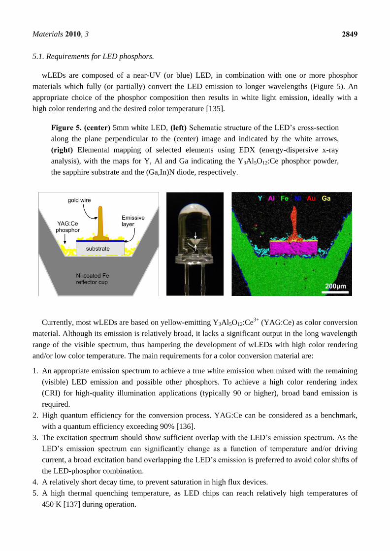
Figure 5. (center) 5mm white LED, (left) Schematic structure of the LED‟s cross-section
along the plane perpendicular to the (center) image and indicated by the white arrows, (right) Elemental mapping of selected elements using EDX (energy-dispersive x-ray
analysis), with the maps for Y, Al and Ga indicating the Y3Al5O12:Ce phosphor powder,
the sapphire substrate and the (Ga,In)N diode, respectively.
Currently, most wLEDs are based on yellow-emitting Y3Al5O12:Ce3+
(YAG:Ce) as color conversion
material. Although its emission is relatively broad, it lacks a significant output in the long wavelength
range of the visible spectrum, thus hampering the development of wLEDs with high color rendering
and/or low color temperature. The main requirements for a color conversion material are:
1. An appropriate emission spectrum to achieve a true white emission when mixed with the remaining
(visible) LED emission and possible other phosphors. To achieve a high color rendering index
(CRI) for high-quality illumination applications (typically 90 or higher), broad band emission is
required.
2. High quantum efficiency for the conversion process. YAG:Ce can be considered as a benchmark,
with a quantum efficiency exceeding 90% [136].
3. The excitation spectrum should show sufficient overlap with the LED‟s emission spectrum. As the
LED‟s emission spectrum can significantly change as a function of temperature and/or driving
current, a broad excitation band overlapping the LED‟s emission is preferred to avoid color shifts of
the LED-phosphor combination.
4. A relatively short decay time, to prevent saturation in high flux devices.
5. A high thermal quenching temperature, as LED chips can reach relatively high temperatures of
450 K [137] during operation.

Materials 2010, 3
2850
6. Good stability during the full lifetime of an LED (typically over 50,000 hours)
The overall efficiency for a wLED is mainly determined by the electrical-to-optical conversion
efficiency of the pumping LED, the Stokes losses associated with the color conversion, the light
extraction efficiency and the quantum efficiency of the phosphor. As the overall efficiency is the
product of all partial efficiencies, it is of utmost importance to carefully select and optimize phosphors
for a quantum efficiency as close to unity as possible, also at elevated operating temperatures.
Requirements 1, 3 and 4 favor the broad band emitting rare earth ions Ce3+
and Eu2+
over most line-
emitting rare earth ions (including Eu3+
), Mn2+
and transition elements. The decay times of Ce3+
(typically 60ns or less, [138]) and Eu2+
(typically 1µs or less, [139]) are sufficiently short to avoid
saturation. Furthermore, these ions present a relatively small Stokes shift, which allows pumping by a
blue LED which reduces conversion losses over UV LEDs, even if the quantum efficiency is close to
unity. Nevertheless, the excitation band width in most compounds is sufficiently broad to allow near-
UV excitation as well.
As there are several sulfide materials which can yield orange-to-red emission, these materials were
recently investigated as conversion phosphor. This ability stands in contrast to oxide hosts, where red
Eu2+
emission is relatively rare [127]. In general, the main criteria for the evaluation of rare-earth
doped sulfides are requirements 5 and 6. Depending on the host‟s composition, the band gap in
sulfides is relatively low, typically in the range from 3 to 5eV. This implies an increased chance of
interaction of the Eu2+
5d orbitals with the conduction band states, thus leading to anomalous emission
[140] or a relatively low quenching temperature. Furthermore, the stability of sulfides is often a matter
of concern as well. In the following discussion, several host materials are discussed in the framework
of the above mentioned requirements. This Section concludes with a comparison to other host
compositions, such as the nitride and oxynitrides.
5.2. Binary sulfides
The luminescence of impurity doped binary, alkaline earth sulfides like MgS, CaS, SrS and BaS has
been extensively studied in the past century. For instance, the rare earths ions (broad band d-f emitters
like Eu2+
and Ce3+
, as well as narrow line f-f emitters), transition metals (Cu+, Ag
+, Mn
2+, Au
+, Cd
2+)
and s² ions (Bi3+
, Pb2+
, Sb3+
,Sn2+
) are all known to luminesce in one or more of the above mentioned
hosts [141]. Several of these host-dopant combinations were studied as thin film EL phosphor (Table
1). Interestingly, undoped CaS and SrS are reported to luminesce as well, although the intensity is far
too low for (LED) applications. The emission wavelength strongly depends on the synthesis
conditions, suggesting the presence of multiple, optically active centers [142,143].
The emission properties of the abovementioned transition metals (except Mn2+
) and the s2 ions are
not very useful for LED color conversion purposes, as they often show considerable thermal
quenching, in combination with a strong temperature dependent spectrum. The latter effect is due to
formation of different emission centers, depending on the dopant concentration and the synthesis
conditions [76,144].
In Table 2, luminescence of alkaline earth sulfides doped with some typical dopants is given.
Especially the data on Eu2+
and Ce3+
doping are interesting as this is valuable information when
considering the emission of these ions in ternary sulfides.
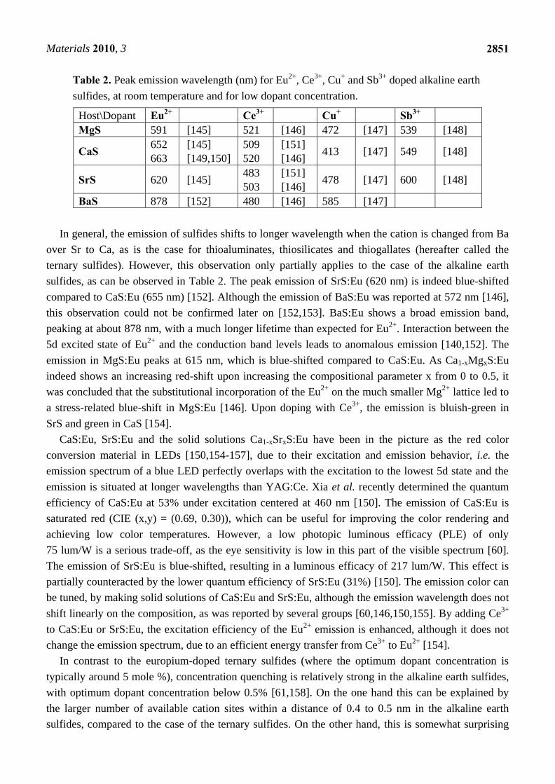
Materials 2010, 3
2851
Table 2. Peak emission wavelength (nm) for Eu2+
, Ce3+
, Cu+ and Sb
3+ doped alkaline earth
sulfides, at room temperature and for low dopant concentration.
Host\Dopant Eu2+ Ce3+ Cu+ Sb3+ MgS 591 [145] 521 [146] 472 [147] 539 [148]
CaS 652
663
[145]
[149,150]
509
520
[151]
[146] 413 [147] 549 [148]
SrS 620 [145] 483
503
[151]
[146] 478 [147] 600 [148]
BaS 878 [152] 480 [146] 585 [147]
In general, the emission of sulfides shifts to longer wavelength when the cation is changed from Ba
over Sr to Ca, as is the case for thioaluminates, thiosilicates and thiogallates (hereafter called the
ternary sulfides). However, this observation only partially applies to the case of the alkaline earth
sulfides, as can be observed in Table 2. The peak emission of SrS:Eu (620 nm) is indeed blue-shifted
compared to CaS:Eu (655 nm) [152]. Although the emission of BaS:Eu was reported at 572 nm [146],
this observation could not be confirmed later on [152,153]. BaS:Eu shows a broad emission band,
peaking at about 878 nm, with a much longer lifetime than expected for Eu2+
. Interaction between the
5d excited state of Eu2+
and the conduction band levels leads to anomalous emission [140,152]. The
emission in MgS:Eu peaks at 615 nm, which is blue-shifted compared to CaS:Eu. As Ca1-xMgxS:Eu
indeed shows an increasing red-shift upon increasing the compositional parameter x from 0 to 0.5, it
was concluded that the substitutional incorporation of the Eu2+
on the much smaller Mg2+
lattice led to
a stress-related blue-shift in MgS:Eu [146]. Upon doping with Ce3+
, the emission is bluish-green in
SrS and green in CaS [154].
CaS:Eu, SrS:Eu and the solid solutions Ca1-xSrxS:Eu have been in the picture as the red color
conversion material in LEDs [150,154-157], due to their excitation and emission behavior, i.e. the
emission spectrum of a blue LED perfectly overlaps with the excitation to the lowest 5d state and the
emission is situated at longer wavelengths than YAG:Ce. Xia et al. recently determined the quantum
efficiency of CaS:Eu at 53% under excitation centered at 460 nm [150]. The emission of CaS:Eu is
saturated red (CIE (x,y) = (0.69, 0.30)), which can be useful for improving the color rendering and
achieving low color temperatures. However, a low photopic luminous efficacy (PLE) of only
75 lum/W is a serious trade-off, as the eye sensitivity is low in this part of the visible spectrum [60].
The emission of SrS:Eu is blue-shifted, resulting in a luminous efficacy of 217 lum/W. This effect is
partially counteracted by the lower quantum efficiency of SrS:Eu (31%) [150]. The emission color can
be tuned, by making solid solutions of CaS:Eu and SrS:Eu, although the emission wavelength does not
shift linearly on the composition, as was reported by several groups [60,146,150,155]. By adding Ce3+
to CaS:Eu or SrS:Eu, the excitation efficiency of the Eu2+
emission is enhanced, although it does not
change the emission spectrum, due to an efficient energy transfer from Ce3+
to Eu2+
[154].
In contrast to the europium-doped ternary sulfides (where the optimum dopant concentration is
typically around 5 mole %), concentration quenching is relatively strong in the alkaline earth sulfides,
with optimum dopant concentration below 0.5% [61,158]. On the one hand this can be explained by
the larger number of available cation sites within a distance of 0.4 to 0.5 nm in the alkaline earth
sulfides, compared to the case of the ternary sulfides. On the other hand, this is somewhat surprising
Materials 2010, 3
2852
given that Eu is easily incorporated in CaS and SrS, as no charge compensation is required and as the
ionic radii of Eu2+
and Sr2+
(and to a somewhat lesser extent Ca2+
) are very similar. Although higher
dopant concentrations are favorable for efficient absorption of the excitation light, it negatively affects
the thermal quenching behavior. In thin films, clustering of Eu dopant ions has been reported [61], thus
increasing the local concentration.
Xia reported a reduction of the emission intensity by about 40% at room temperature, compared to
the intensity at 20 K, for a dopant concentration of 0.3 mole % in Ca0.8Sr0.2S:Eu [150]. Nevertheless,
the emission was only quenched to 50% at 420 K, in comparison to the low temperature case. This
observation, typical for Ca1-xSrxS:Eu, shows that the thermal quenching profile deviates from the
profile observed in most ternary compounds where the thermal quenching manifests itself in a rather
narrow temperature region. Given that the T0.5 (i.e. the temperature when the emission intensity is
halved compared to the low temperature case) has been reported at 475 K for CaS:Eu and 320 K for
SrS:Eu [159], it is questionable whether Ca1-xSrxS:Eu phosphors with higher Sr concentrations are
ideal for use in LEDs.
The stability of the alkaline earth sulfides CaS and SrS is reasonable, although slow decomposition
in moist air is observed. In the case of MgS:Eu, Kasano et al. reported its stability to be much better
when the powder was fully sulfurized [146]. Besides the reduction in light output, Shin et al. reported
another detrimental effect of the decomposition of CaS:Eu upon application in LEDs, namely a
chemical reaction of the released H2S with the Ag pad under the LED chip, thus reducing the
reflectivity [160]. Several encapsulation methods have been recently proposed, all reducing the
decomposition rate under accelerated ageing conditions (high temperature and high humidity). These
methods include coating with Al2O3 using atomic layer deposition [161], an organic-SiO2
nanocomposite [162,163] or a thin BN sheet [164].
5.3. Thiogallates.
In the early 1970‟s, the luminescence of several europium-doped thiogallates was described (Table
3), with the peak emission wavelength red-shifting when going from BaGa2S4:Eu (490 nm) over
SrGa2S4:Eu (538 nm) to CaGa2S4:Eu (560 nm) [165,166]. Some luminescent thiogallate phosphors
with deviating 1:2:4 stoichiometry can also be synthesized, such as Sr2Ga2S5:Eu and BaGa4S7:Eu,
while other compositions are thermally quenched at room temperature (e.g. Ba3Ga2S6:Eu and
Ba4Ga2S7:Eu) [167].

Materials 2010, 3
2853
Table 3. Emission properties of Eu2+
and Ce3+
doped thiogallate phosphors. x% quenching
indicates the fraction of the emission intensity at room temperature compared to the low
temperature intensity. xK is the temperature for which the emission intensity is half that at
low temperature.
Host Dopant max(nm) Quenching Remarks Ref. MgGa2S4 Eu
2+ 660 [168]
CaGa2S4 Eu2+
Ce3+
565
459
410 K [91]
[169]
SrGa2S4 Eu2+
Ce3+
534
445
470 K [95]
[170]
Sr2Ga2S5 Eu2+
553 (90 K) 280 K [166]
BaGa4S7 Eu2+
482 (90 K) 70% [166]
BaGa2S4 Eu2+
Ce3+
493
448
420 K [171]
[170]
Ba2Ga2S5 Eu2+
- No emission at 90
K
[167]
Ba3Ga2S6 Eu2+
538 (90 K) 140 K [167]
Ba4Ga2S7 Eu2+
654 (90 K) 110 K [167]
Ba5Ga2S8 Eu2+
- No emission at 90
K
[167]
EuGa2S4 Eu2+
546 +/- 150 K [166,172]
ZnGa2S4 Eu2+
540 [173]
As the quantum efficiency of CaGa2S4:Eu and Sr2Ga2S5:Eu was reported to be similar to that of
YAG:Ce [174], the thiogallates recently attracted attention as color conversion phosphor as well
[174-179]. The emission band width is considerably smaller than in YAG:Ce, which necessitates the
use of at least a second, red-emitting phosphor to produce white light starting from a blue LED.
Several authors reported the combination of CaS:Eu and CaGa2S4:Eu [175,177,179], even with a „one
pot synthesis‟ based on the observation that a CaS:Ga2S3 starting ratio higher than 1:1 leads to a
mixture of CaS:Eu and CaGa2S4:Eu. Taking into account that CaS:Eu has a much more severe
concentration quenching behavior compared to CaGa2S4:Eu, it is questionable whether this synthesis
approach is optimal in terms of overall quantum efficiency of the mixture.
Yu et al. described the structural and luminescent properties of Ca1-xSrx(Ga1-yAly)2S4:Eu2+
phosphors [174]. Changing the values of x and y, a single crystallographic phase is obtained over the
entire range. The luminescence shifts almost linearly on the composition, which allows continuous
tuning of the peak emission wavelength from 496 nm (SrAl2S4:Eu) to 556 nm (CaGa2S4:Eu), while
keeping a narrow emission band, indicated by a FWHM of about 40 nm.
In view of LED applications, the thermal quenching behavior is reasonable for the MGa2S4:Eu
compounds (T0.5 = 420 K for BaGa2S4:Eu [171], 470 K for SrGa2S4:Eu [95] and 400 K for CaGa2S4:Eu
[180]) allowing remote phosphor approaches, while it is worse for thiogallates with different alkaline
earth to gallium ratio [167].
Materials 2010, 3
2854
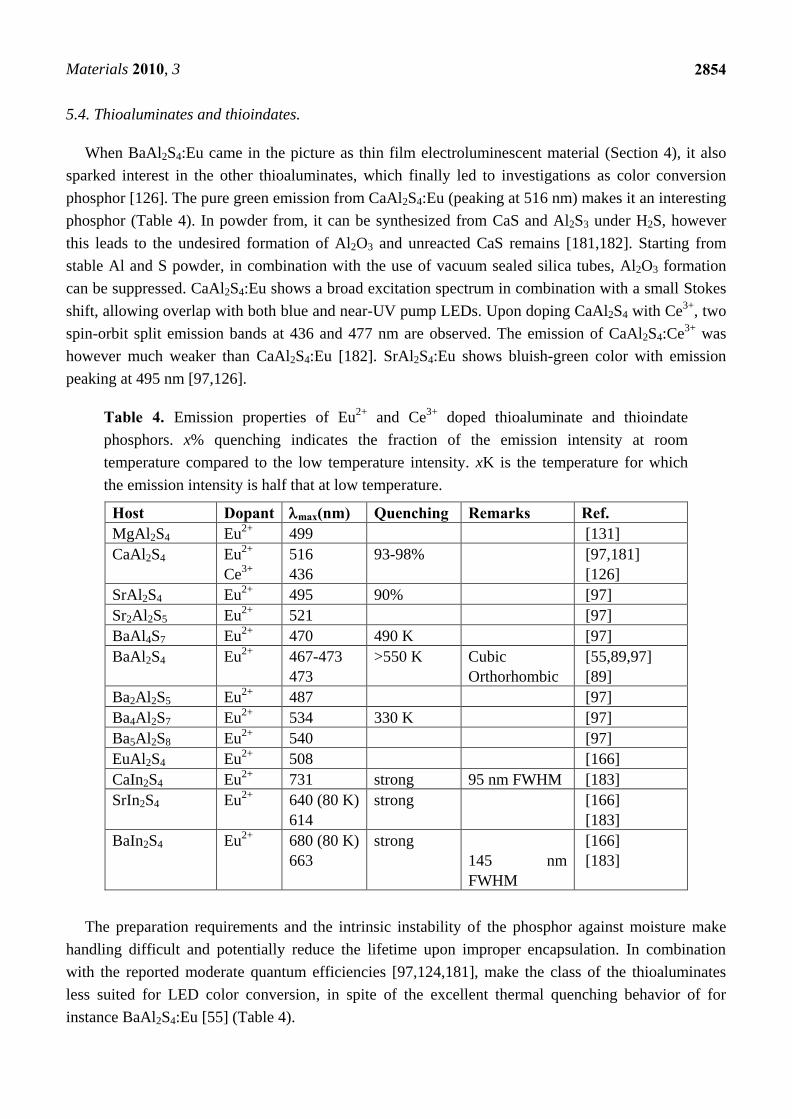
5.4. Thioaluminates and thioindates.
When BaAl2S4:Eu came in the picture as thin film electroluminescent material (Section 4), it also
sparked interest in the other thioaluminates, which finally led to investigations as color conversion
phosphor [126]. The pure green emission from CaAl2S4:Eu (peaking at 516 nm) makes it an interesting
phosphor (Table 4). In powder from, it can be synthesized from CaS and Al2S3 under H2S, however
this leads to the undesired formation of Al2O3 and unreacted CaS remains [181,182]. Starting from
stable Al and S powder, in combination with the use of vacuum sealed silica tubes, Al2O3 formation
can be suppressed. CaAl2S4:Eu shows a broad excitation spectrum in combination with a small Stokes
shift, allowing overlap with both blue and near-UV pump LEDs. Upon doping CaAl2S4 with Ce3+
, two
spin-orbit split emission bands at 436 and 477 nm are observed. The emission of CaAl2S4:Ce3+
was
however much weaker than CaAl2S4:Eu [182]. SrAl2S4:Eu shows bluish-green color with emission
peaking at 495 nm [97,126].
Table 4. Emission properties of Eu2+
and Ce3+
doped thioaluminate and thioindate
phosphors. x% quenching indicates the fraction of the emission intensity at room
temperature compared to the low temperature intensity. xK is the temperature for which
the emission intensity is half that at low temperature.
Host Dopant max(nm) Quenching Remarks Ref. MgAl2S4 Eu
2+ 499 [131]
CaAl2S4 Eu2+
Ce3+
516
436
93-98%
[97,181]
[126]
SrAl2S4 Eu2+
495 90% [97]
Sr2Al2S5 Eu2+
521 [97]
BaAl4S7 Eu2+
470 490 K [97]
BaAl2S4 Eu2+
467-473
473
>550 K Cubic
Orthorhombic
[55,89,97]
[89]
Ba2Al2S5 Eu2+
487 [97]
Ba4Al2S7 Eu2+
534 330 K [97]
Ba5Al2S8 Eu2+
540 [97]
EuAl2S4 Eu2+
508 [166]
CaIn2S4 Eu2+
731 strong 95 nm FWHM [183]
SrIn2S4 Eu2+
640 (80 K)
614
strong [166]
[183]
BaIn2S4 Eu2+
680 (80 K)
663
strong
145 nm
FWHM
[166]
[183]
The preparation requirements and the intrinsic instability of the phosphor against moisture make
handling difficult and potentially reduce the lifetime upon improper encapsulation. In combination
with the reported moderate quantum efficiencies [97,124,181], make the class of the thioaluminates
less suited for LED color conversion, in spite of the excellent thermal quenching behavior of for
instance BaAl2S4:Eu [55] (Table 4).

Materials 2010, 3
2855
Upon consideration of the interesting properties of the alkaline earth thioaluminate and thiogallate
phosphors, one might also consider the thioindate phosphors, for which a red-shifted emission can be
anticipated. However, the relatively small bandgap of these materials compared to the thioaluminates
and thiogallates [184], leads to anomalous emission and/or strong thermal quenching due to the
increased interaction of the 5d excited states of Eu2+
and the conduction band states [159]. For instance
BaIn2S4 and CaIn2S4, both show a strongly broadened and weak emission at room
temperature [166,183].
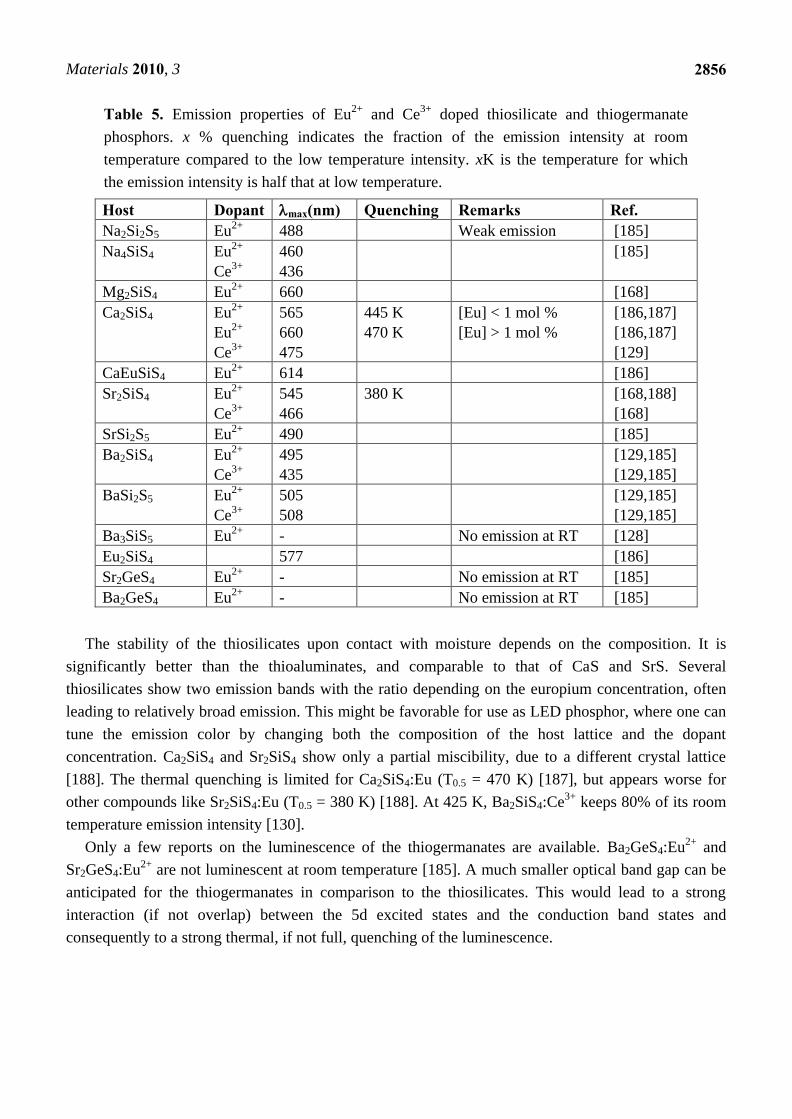
5.5. Thiosilicates and thiogermanates.
The emission of thiosilicate hosts upon doping with Ce3+
and Eu2+
covers the entire range from
deep-blue (Ba2SiS4:Ce3+
) to saturated red (Ca2SiS4:Eu2+
) [129,168]. Figure 6 gives an overview of the
emission colors that can be obtained. In general, Ce3+
doping is less efficient and the optimal dopant
concentration is fairly low. Adding Al3+
as a co-dopant to Ba2SiS4:Ce3+
improves the crystallinity, the
luminescence intensity and the dopant incorporation [130]. An internal quantum efficiency of 36%
was reported.
Ca2SiS4:Eu2+
shows two emission bands, at 565 nm and 660 nm [186], with the ratio between both
bands depending on the europium concentration (Table 5). The solubility of Eu2+
in the orthorhombic
Ca2SiS4 host is limited to about 10%. For higher concentrations, a second, monoclinic phase similar to
Eu2SiS4 is formed [189]. The fully substituted compound Eu2SiS4 is still luminescent, although the
emission efficiency is considerably quenched [186,190]. Moreover, the practical application of such a
fully substituted phosphor would be limited due to the prohibitively high cost of europium. It is
interesting to note that also EuGa2S4 and EuAl2S4 show luminescence at room temperature, while EuS
does not [166,191,192].
Figure 6. Emission colors of europium and cerium doped thiosilicates. Dopant
concentration is 1mol %, unless otherwise specified [129,186,188].
Materials 2010, 3
2856
Table 5. Emission properties of Eu2+
and Ce3+
doped thiosilicate and thiogermanate
phosphors. x % quenching indicates the fraction of the emission intensity at room
temperature compared to the low temperature intensity. xK is the temperature for which
the emission intensity is half that at low temperature.
Host Dopant max(nm) Quenching Remarks Ref. Na2Si2S5 Eu
2+ 488 Weak emission [185]
Na4SiS4 Eu2+
Ce3+
460
436
[185]
Mg2SiS4 Eu2+
660 [168]
Ca2SiS4 Eu2+
Eu2+
Ce3+
565
660
475
445 K
470 K
[Eu] < 1 mol %
[Eu] > 1 mol %
[186,187]
[186,187]
[129]
CaEuSiS4 Eu2+
614 [186]
Sr2SiS4 Eu2+
Ce3+
545
466
380 K [168,188]
[168]
SrSi2S5 Eu2+
490 [185]
Ba2SiS4 Eu2+
Ce3+
495
435
[129,185]
[129,185]
BaSi2S5 Eu2+
Ce3+
505
508
[129,185]
[129,185]
Ba3SiS5 Eu2+
- No emission at RT [128]
Eu2SiS4
577 [186]
Sr2GeS4 Eu2+
- No emission at RT [185]
Ba2GeS4 Eu2+
- No emission at RT [185]
The stability of the thiosilicates upon contact with moisture depends on the composition. It is
significantly better than the thioaluminates, and comparable to that of CaS and SrS. Several
thiosilicates show two emission bands with the ratio depending on the europium concentration, often
leading to relatively broad emission. This might be favorable for use as LED phosphor, where one can
tune the emission color by changing both the composition of the host lattice and the dopant
concentration. Ca2SiS4 and Sr2SiS4 show only a partial miscibility, due to a different crystal lattice
[188]. The thermal quenching is limited for Ca2SiS4:Eu (T0.5 = 470 K) [187], but appears worse for
other compounds like Sr2SiS4:Eu (T0.5 = 380 K) [188]. At 425 K, Ba2SiS4:Ce3+
keeps 80% of its room
temperature emission intensity [130].
Only a few reports on the luminescence of the thiogermanates are available. Ba2GeS4:Eu2+
and
Sr2GeS4:Eu2+
are not luminescent at room temperature [185]. A much smaller optical band gap can be
anticipated for the thiogermanates in comparison to the thiosilicates. This would lead to a strong
interaction (if not overlap) between the 5d excited states and the conduction band states and
consequently to a strong thermal, if not full, quenching of the luminescence.

Materials 2010, 3
2857
5.7. Future
The past years were characterized by a strong research interest in color conversion phosphors for
LEDs. The lack of phosphors with sufficient emission intensity in the red part of the visible spectrum
can be overcome with certain (Eu2+
-doped) sulfide phosphors. As discussed above, several sulfide
phosphors are well suited as color conversion material, provided that their thermal quenching behavior
and quantum efficiency are meticulously studied. Currently, these aspects are often lacking in recently
published work on (sulfide) conversion phosphors. When compared to other recently proposed hosts,
such as the nitrides [135,193,194] and oxynitrides [195,196], the sulfides have the disadvantage of a
much lower stability, although this could be improved upon proper encapsulation, which can both be
achieved at the level of a single phosphor particle or by incorporation in an impermeable matrix. Of
course, when considering the expected lifetime of an LED being in the range of 10-50 khours, one
would rather use the most stable phosphor host available.
6. Persistent Luminescence and Storage Phosphors
Persistent phosphors are materials which can emit light up to hours after the (optical) excitation has
ceased. Since more than a decade, green-emitting SrAl2O4:Eu,Dy has replaced ZnS:Cu,Co, due to its
better stability and longer afterglow [197]. Several other efficient materials were developed, especially
in the short wavelength range of the visible spectrum, such as CaAl2O4:Eu,Nd (violet, [198]) and
Sr2MgSi2O7:Eu,Dy (blue, [199]). A review of the reported persistent phosphors and the different
models which have been proposed can be found in this „Special Issue‟ [200]. Yellow and red persistent
phosphors with high initial brightness are relatively scarce, which is partially due to the reduced eye
sensitivity at low light intensity levels and the limited number of host materials for Eu2+
yielding red
emission [201]. Moreover, a new standard was proposed to accurately describe persistent phosphors
when light levels are below 1 cd/m² [201,202]. The development of bright red persistent phosphors
would open a new range of applications, for instance in emergency signage.
To obtain persistent luminescence in the long wavelength range of the visible spectrum, one could
either look at Eu3+
based materials or specific Eu2+
activated sulfides. Y2O2S:Eu3+
codoped with Ti and
Mg is one of the few red persistent phosphors, but it cannot efficiently be excited by visible light and
the afterglow is relatively short [203].
As CaS:Eu2+
and SrS:Eu2+
are able to yield red and orange emission respectively, they have
attracted some attention as persistent phosphor as well. SrS:Eu2+
often shows some afterglow even
without (intentional) co-doping [204], which is possibly related to synthesis conditions promoting
sulfur deficiency. The addition of Dy3+
somewhat enhances the afterglow, although it remains short
and relatively weak [205,206]. The addition of Cl
- to CaS:Eu yields an afterglow in the deep-red region with slightly red-shifted
emission compared to CaS:Eu [207]. Addition of trivalent ions such as Y3+
, Al3+
and Tm3+
to CaS:Eu
gives moderate (Y, Al) to bright afterglow (Tm) [208,209], while adding Na+ to CaS:Eu,Tm reduces it,
suggesting a significant role for the charge compensating defects.
Upon adding Sm3+
to CaS:Eu [210], a photo stimulable phosphor (rather than a persistent phosphor)
is obtained as the trap levels introduced by Sm3+
are too deep to be thermally emptied. However, upon
illumination of the material with infrared excitation, visible emission can be obtained (provided the

Materials 2010, 3
2858
powder has previously been excited by UV or visible light, x-rays…, which discriminates it from an up
conversion phosphor). The exact defect structure caused by the introduction of the rare earth ions and
its influence on the energy level scheme has not been fully established yet [211,212]. Furthermore, the
phosphor‟s behavior strongly depends on the concentrations of the Sm and Eu dopants [213]. Jia et al.
also reported that the addition of Tm3+
to Ca0.9Sr0.1S:Bi3+
prolongs and intensifies the (blue) afterglow
in this material [214]. A relatively short and weak afterglow could be obtained upon co-doping of
CaGa2S4:Eu, with the best result for Ho3+
[101,215].
Recently, persistent luminescence in Ca2SiS4:Eu,Nd was reported, with the main emission band
peaking at 660 nm [187]. Practical usage seems limited, as excitation below 360 nm is required to
induce the persistent luminescence. In addition, the perceived emission intensity is relatively low, due
to the eye sensitivity which drops rapidly at decreasing light levels at this long wavelength [201].
Nevertheless, it could be interesting from a fundamental point of view, as it was shown that transfer of
charge carriers via the conduction band must be limited and that the Nd3+
codopants (and associated
charge compensating defects) most probably reside in the proximity of the Eu2+
ions [187].
Most of the time, persistent phosphors are applied as luminous paint, for instance in emergency exit
indicators. Hence they are required to have long lifetimes in often relatively harsh environments. Even
with adequate encapsulation, the intrinsic instability of phosphor hosts like CaS, SrS or Ca2SiS4
appears unfavorable for persistent luminescence applications.
7. Luminescent Sulfide Nanoparticles
7.1. Undoped nanoparticles
7.1.1. Introduction
Colloidal semiconductor nanocrystals or quantum dots (Qdots) offer an interesting alternative to
Ce3+
- or Eu2+
- doped bulk sulfide materials. When their radius R is smaller than the bulk exciton Bohr
radius RB, their electronic properties, most importantly the Qdot band gap, become size-dependent
[216]. In this regime, termed the strong quantum confinement regime, the Qdot eigenstates form a
discrete set instead of the quasi-continuum of states found in bulk semiconductors. To illustrate this,
let us first assume that a Qdot can be regarded as an infinite spherical quantum well. The eigenenergies
Elk of a particle with mass m0 in this infinite well are given by:
2
0
22
2 Rm
uE lk
lk
ulk denotes the k-th zero of the BesselJ-function of order l. Clearly, every energy level Elk increase
with the inverse of the square of the particle radius R. A more rigorous calculation of the Qdot
eigenstates accounts for a shielded Coulomb attraction between the electron and hole which constitute
the exciton formed after excitation. This correction scales with R-1
, and we obtain following size-
dependence for the Qdot band gap E0 (Brus-equation, [216] Eg: bulk band gap; me: electron effective
mass; mh: hole effective mass, ε dielectric constant):
Materials 2010, 3
2859
R
e
mmREE
he
g
2
2
22
0
8.111
2
Conveniently, the blue shift of the band gap with decreasing Qdot size allows covering a large part
of the electromagnetic spectrum by a single material. Taking the cadmium salt Qdots as an example:
CdS emits violet to blue light, CdSe emits from blue to red and the CdTe emission can be tuned from
green to deep red [217], [218].
Most semiconductor Qdot materials can be synthesized with a high photoluminescence quantum
yield, which is often accomplished by coating the Qdot core with an inorganic shell [219]. This shell,
typically consisting of ZnS, has a larger band gap than the Qdot core and thus prohibits a penetration
of the exciton wavefunction into the shell (type-I core-shell Qdots, both carriers localized in the Qdot
core). It effectively shields the exciton from the surface; hence, possible surface states no longer lead
to a quenching of the Qdot luminescence and Qdots with a high quantum yield are obtained. For
instance, quantum yield values of up to 60% have been reported for CdSe/ZnS and InP/ZnS core-shell
Qdots [219].
Coating procedures can also be used to further engineer the Qdot band gap. Instead of using a high
band gap shell material (such as ZnS), two materials with a large bulk band offset can be combined. In
this case, the staggered band alignment leads to a spatially separated exciton, where the electron for
instance remains in the Qdot core while the hole is transferred to the shell (type-II core-shell Qdots).
An indirect band gap is formed which may be, depending on the core size and shell thickness,
narrower than the bulk band gap of both constituents. CdS/ZnSe for instance can be synthesized with
an absorption onset down to 650 nm, while both bulk materials have an absorption onset of 515 nm
and 460 nm, respectively [219].
The versatile band gap tuning and high photoluminescence quantum yield has lead to a diverse
range of applications based on colloidal Qdots; they are currently used as luminescent biomarkers
[220,221] and in light-emitting diodes [222-225] and lasers [226-228]. Clearly, colloidal
semiconductor Qdots have a large potential, however covering the broad range of materials and
applications is beyond the scope of this review. We refer to the review by Bera et al. [229] for a more
detailed discussion. Here, we will limit ourselves to sulfide Qdots, in casu CdS and PbS, and the
applications realized with these materials.
7.1.2. Brief historic overview of sulfide Qdots
During the pioneering years of research on quantum dots (Qdots), now thirty years ago, metal
sulfide nanocrystals were among the first materials to be synthesized. Following the groundbreaking
theoretical work of Brus [216] and Efros and Efros [230], who calculated that quantum confinement
induces a discretization of the electronic band structure and a blue shift of the band gap in small
semiconductor nanocrystals, several research groups indeed succeeded in the synthesis of metal sulfide
Qdots, more specifically CdS and PbS, either in solution [231-234], in polymers [235,236] or in a glass
host [237-240]. As a result of the small nanocrystal size, typically a few nanometer (Figure 7), the
Qdot band gap was clearly shifted to higher energies and pronounced absorption peaks, due to
transitions between the discrete Qdot energy levels, appeared in the spectrum (Figure 8).

Materials 2010, 3
2860
However, the typical Qdot photoluminescence yield in these materials was low, and the Qdots often
suffered from trap emission due to the high surface-to-volume ratio. Although Henglein [232]
successfully increased this yield to 50% by a coating of CdS particles with Cd(OH)2, this problem was
remedied more efficiently by the development of a high temperature organic phase synthesis,
described by Murray et al. in 1993 [241]. High-quality colloidal CdX (X = S, Se, Te) Qdots of uniform
size were prepared by their method. Furthermore, a proper passivation of the surface by organic
ligands ensured a high photoluminescence yield. Consequently, this paper sparked a strong interest in
colloidal Qdots.
Figure 7. Transmission electron microscopy image of a single PbS nanocrystal (Reprinted
with permission from [231]. Copyright 1985 American Institute of Physics).
Figure 8. (left) Absorbance spectra of CdS Qdots of radius 32 nm (1), 2.3 nm (2), 1.5 nm
(3) and 1.2 nm (4), (right) absorbance spectra of 31 nm (1), 2.9 nm (2) and 2.0 nm (3)
CuCl Qdots (Reprinted from [237] with permission from Elsevier).

Materials 2010, 3
2861
7.1.3. State-of-the-art
Currently, both CdS and PbS Qdots are widely investigated, especially since the development of
high quality synthesis routes employing greener chemicals. For the production of CdS Qdots, Peng et
al. replaced the dimethyl cadmium employed by Murray et al. [241] with Cd-phosphonate or Cd-
carboxylate complexes, which were prepared by reacting CdO with the respective long-chained acid
[217,218]. As the bulk band gap for CdS equals 2.41 eV [242], these synthesis schemes usually yield
Qdots with an emission tunable from the blue to the near UV (Figure 9). Reported quantum
efficiencies for CdS Qdots produced by similar methods typically vary between 3 and 12% [243,244],
although it can be increased to 30-40% by coating the Qdots with a protective ZnS shell [244,245].
Similarly, encapsulating them with 2-mercaptopropionic acid increases the luminescence yield to ca.
50% [246].
Figure 9. Series of absorbance (full lines) and luminescence spectra (dotted lines) of CdS
Qdots of varying size. (Reprinted from [217] with permission. Copyright Wiley-VCH
Verlag GmbH & Co. KGaA.).
With a bulk band gap of 0.41 eV, PbS Qdots are an ideal material for NIR imaging [248],
photodetectors and photovoltaics [249-253] and telecom applications [227,254]. In 2003, two
important colloidal synthesis routes for PbS Qdots were proposed. They differ significantly, the
method of Hines et al. [255] being based on leadoleate and bis(trimethylsilyl)sulfide, while Joo
et al. [256] (and later Cademartiri et al. [247]) start from PbCl2 and elemental sulphur dissolved in
oleylamine. However, both lead to monodisperse PbS Qdot suspensions, indicated by the sharp
absorption and luminescence features of the Qdots (Figure 10). They possess a strong band gap

Materials 2010, 3
2862
luminescence in the NIR (Figure 10), with quantum yields ranging between 20 and 80%
[247,255,257]. Interestingly, the luminescence decay time in these materials is quite long (typically a
few µs) [258], comparable to PbSe Qdots [259], but much longer than CdX materials, which have a
decay time of the order of 10-50 ns [246,260,261]. Recent results have shown that a strong local field
effect in PbS Qdots [262] leads to this long decay time, although the different band structure may also
play a role here.
Figure 10. Series of luminescence (a) and absorbance spectra (b) of PbS Qdots of varying
size. (Reprinted with permission from [247]. Copyright 2006 American Chemical Society).
7.1.4. Applications of luminescent metal sulfide Qdots
Due to their bright luminescence, both CdS and PbS Qdots are interesting materials for photonic
devices based on light emission. Hence, the observation of amplified spontaneous emission and gain in
visible [260,263,264] and NIR [265-267] Qdot materials rapidly led to the development of Qdot lasers.
For instance, using CdS Qdots, an optically pumped blue laser was recently demonstrated [228]. The
Qdot emission was coupled to the whispering gallery modes of a glass microsphere, and above a
threshold of ~60µW (corresponding to a fluence of 3.7 mJ/cm2), lasing was observed. Similarly, PbS
Qdots have been used by Hoogland et al. [227] to produce a laser operating at telecom wavelengths
(1.53 µm in this case). By coating the inner walls of a glass microcapillary tube, the emission was
again coupled to the whispering gallery modes of the cavity, leading to efficient lasing above a
threshold fluence of 177 µJ/cm2 (Figure 11).

Materials 2010, 3
2863
Figure 11. (a) Absorption spectrum (full line) and below-threshold photoluminescence
spectrum at room temperature (dashed line) and 80 K (dotted line) of PbS Qdots. The
sharp peak corresponds to the emission spectrum of the Qdot microcapillary laser when
pumped above threshold. (b) Pump fluence dependence of the Qdot emission. The
threshold behavior and representative emission spectra (insets) clearly demonstrate lasing.
(permission requested, adapted from [227]).
Next to emission due to photoexcitation, colloidal Qdots can also be excited by electrical pumping.
The demonstration of electroluminescence [268-270] was therefore an important step forward in the
fabrication of light-emitting devices (LEDs). Following these early experiments, Qdot LEDs based on
CdS (Figure 12) [222] and PbS [223] Qdots have been reported. While PbS Qdots offer the unique
possibility of having efficient NIR LEDs over a wide spectral range, unfortunately, in the case of CdS,
we are restricted to the blue part of the electromagnetic spectrum. Other CdX materials and
compositions are needed to enable LED fabrication over the remaining visible spectrum [224,225].
However, as reported by Anikeeva et al., in the blue spectral region important challenges remain, as
the external quantum efficiency is low [224]. A value of only 0.4% was obtained for a blue LED
employing ZnCdS Qdots coated with a ZnS shell, compared to an efficiency of 2.6% for a green LED.
This implies that there is still plenty of room for optimization, either through device fabrication or an
improvement of the active material.
Figure 12. Electroluminescence spectrum of a CdS Qdot LED, measured at a bias of 5.5
V. Inset: images of the LED. (Reprinted with permission from [222]. Copyright 2007
American Chemical Society.).
Materials 2010, 3
2864
7.2. Doped nanoparticles
During the past decade, the strong research effort in semiconductor quantum dots also sparked
interest into doped quantum dots, being the nano-sized counterpart of the well-studied rare earth and
transition metal doped bulk phosphors. Regardless of the exact composition of these nano-materials, it
is not a priori clear whether reducing the particle‟s size is favorable for the luminescence properties of
the dopants (having localized transitions). The increase in band gap which follows the decrease in size
might be favorable for the thermal quenching behavior, while the increased surface-to-volume ratio
offers additional non-radiative decay routes. The main obstacle, however, is the effective incorporation
of the dopant ions into the nanoparticles, rather than simply decorating the particles‟ surface. As hardly
any work has been reported on ternary sulfides, except for some top-down approaches, where particle
size is reduced by ball-milling [271], we will focus on doped „simple sulfides‟ like ZnS, CaS and SrS.
ZnS:Mn is probably the most studied doped sulfide in nano-sized form, due to the chemical
similarity between Zn2+
and Mn2+
, facilitating the incorporation of the dopant ion. Nevertheless, the
incorporated concentration is consistently lower than the intended dopant concentration [272] and part
of the Mn2+
ions reside near the surface of the nanoparticle. The work by Bol et al. showed that the
lifetime of Mn2+
in ZnS:Mn2+
quantum dots is very similar to the bulk lifetime [273,274], in spite of
earlier work stating a considerable shortening of the lifetime [275]. Also the emission spectrum itself is
almost size-independent [272,274]. Hence, growing an inorganic (ZnS) shell around ZnS:Mn
effectively reduces non-radiative decay paths and enhances the luminescence [276], more efficiently
than organic passivation of the surface [272]. Synthesis techniques, luminescence properties and
possible applications of ZnS:Mn nanoparticles can be found in the Reviews by Chen et al. [277] and
Yang et al. [272].
For the solvothermal synthesis of ZnS, Biswas and Kar investigated the influence of precursors,
solvents and temperature on the crystallographic phase formation (cubic and hexagonal), morphology
(particles, rods and sheets) and size (few nm to micron size) [278]. Some reports are available on the
luminescence of nano-sized ZnS:Eu, although the results are diverging, with the presence of both Eu3+
and (assumed) Eu2+
emission [279-281]. Bulk ZnS:Eu is not luminescent and it was supposed that
increasing the band gap of the host would allow the 5d-4f transition in Eu2+
. Incorporation of Eu in the
first place appears difficult in ZnS, due to the strongly different ionic radius of Zn2+
and Eu2+
[282].
AC electroluminescence was reported using ZnSe/ZnS:Mn/ZnS core/shell nanoparticles with a high
photoluminescent quantum efficiency of 65% [283]. The semiconductor part of the ACTFEL devices
consisted of a multi-layer of spin-casted nanoparticles layers (thickness of 30 nm) and sputtered
(undoped) ZnS layers (12 nm). The typical orange ZnS:Mn emission was obtained for these structures,
with a brightness of 2 cd/m² at 30 kHz, while devices without the sputtered ZnS layers didn‟t show EL
emission. Toyama et al. did obtain EL in a 150 nm thick printed layer of ZnS:Mn nanoparticles. At 5
kHz, and 45 V above threshold, a luminance of 1cd/m2 could be obtained for the smallest particles
(3 nm) [284].
The doped „simple sulfides‟, like CaS and SrS, have recently attracted some attention in their nano-
sized form. Several synthesis methods have been proposed for the synthesis of CaS and SrS, such as a
precipitation method (using chloride precursors and sodium sulfide [285,286]) and an alkoxide method
(using H2S as sulfur source [285]). With both methods, particle sizes in the range from 15 to 25 nm

Materials 2010, 3
2865
could be obtained. Upon doping with Eu2+
, the as-prepared particles are not luminescent and EPR
(electron-paramagnetic resonance) shows the europium ions are not incorporated in the particles yet (at
least not in their divalent state). After a thermal annealing at typically 700 °C, luminescent
nanoparticles are obtained, with emission and excitation spectra rather similar to the bulk counterparts
[285,286]. Other methods using a reducing atmosphere at high temperature were proposed for the
preparation of SrS:Eu,Dy and SrS:Cu nanoparticles [205,287].
A solvothermal method was also reported to obtain doped sulfides, such as CaS:Pb, CaS:Ag and
CaS:Bi [288,289]. Chloride precursors, elemental sulfur, ethylenediamine and capping agents are
heated to about 170 to 220 °C in a teflon-lined autoclave for several hours. Particles with a relatively
broad size range are obtained, ranging from tens to hundreds of nm. No thermal annealing is required
to obtain luminescent particles. Modifications to this solvothermal synthesis using ethylenediamine as
mentioned above, allowed the formation of nicely faceted, sub-micron to micron-sized Ca1-xSrxS single
crystals [155] [149,155]. Incorporation of dopant ions (Eu2+
and Ce3+
) is straightforward and leads to
bright luminescence, without the need for a high-temperature annealing step. Hence, the temperature
of the entire synthesis process is limited to 200 °C, and no H2S gas is used.
Whispering gallery modes (WGMs) were observed in Eu2+
and Ce3+
-doped CaS and SrS particles,
which were related to resonance modes in the equatorial planes of the octahedron shaped crystals
[290]. A modification of this solvothermal method allowed the growth of oriented and textured CaS:Eu
and SrS:Eu thin films, which showed bright photoluminescence, with emission properties in line with
bulk phosphors, and AC electroluminescence when electrically contacted [291].
Recently, CaS:Eu nanowires with a high aspect ratio and diameter between 50 and 150 nm were
prepared using a (molten) B2O3 matrix [164]. Unlike most of the nano-sized doped sulfides mentioned
in this section, the Eu2+
emission spectrum deviates from the bulk phosphor, with a blue-shift of about
30 nm.
8. Conclusions
In this Review, we attempted to give an account of the rich history of sulfides for a wide range of
luminescence applications. Without any doubt, the sulfides possess specific properties which made
them especially suited as powder electroluminescent phosphor (based on ZnS:Cu) or as thin film
electroluminescent material, where one should highlight the yellow-orange-emitting ZnS:Mn and the
blue BaAl2S4:Eu phosphor. However, the future looks rather dim for these lighting and display
techniques, due to the advent of superior techniques, like organic LEDs and liquid crystal displays. It
is interesting to note that both in powder and thin film EL, the amount of research and development
has always been relatively small, compared to the effort put into other techniques. Nevertheless, as
thin film electroluminescence has some intrinsic advantages, it might still have a future as a full-color
display technique in demanding environments.
The future of sulfide phosphors could be situated in the field of color conversion for white LEDs.
Upon doping with Eu2+
and Ce3+
, the emission can be tuned from deep blue to saturated red by
appropriately choosing the host composition. In general, the emission and excitation bands are
sufficiently broad, allowing both a good color rendering and efficient pumping by the LED. Two
major criteria should however be systematically evaluated, namely the quantum efficiency of

Materials 2010, 3
2866
photoluminescence and the thermal quenching behavior (both in terms of intensity reduction and
spectral shift). Even if „ideal‟ host-dopant combinations are found, the preparation conditions and the
long term stability of sulfides will largely determine whether they are to be incorporated in LEDs after
all. Fine tuning of synthesis conditions and the application of protective coatings are two major
research tracks to be considered.
CdS and PbS quantum dots have already shown unique abilities and future potential as luminescent
material for a wide range of photonic applications, both in the visible and the near-infrared. However,
from environmental point of view, the toxicity of both Pb and Cd remains a serious issue, hampering
their large scale application. Doped semiconductor nanoparticles (based on sulfides) have probably not
shown their full potential yet, as the incorporation of the dopants into the nanoparticles appears to be
non-trivial.
Acknowledgements
PFS and IM are post-doctoral researchers for the Fund for Scientific Research – Flanders (FWO-
Vlaanderen). This research was carried out under the Interuniversity attraction poles programme
IAP/VI-17 (INANOMAT) financed by the Belgian State, Federal science policy office.
References and Notes
1. Yen, W.M.; Weber, M.J. Inorganic Phosphors: Compositions, Preparation and Optical
Properties; CRC Press: Boca Raton, FL, USA, 2004.
2. Yen, W.M.; Shionoya, S.; Yamamoto, H. Phosphor Handbook, 2nd ed.; CRC Press: Boca Raton,
FL, USA, 2007.
3. Harvey, E.N. A History of Luminescence From the Earliest Times Until 1900; American
Philosophical Society: Philadelphia, PA, USA, 1957.
4. Leverenz, H.W. An Introduction to Luminescence of Solids; Wiley: New York, NY, USA, 1950.
5. Sidot, T. Recherches sur la crystallisation de quelque sulphures métalliques et sur les propriétés
de la blende hexagonale. Comptes Rend. Ac. Sci. 1866, 62, 999-1001.
6. Wiedemann, E. Uber Fluorescenz und Phosphorescenz. Ann. der Physik 1888, 34, 446-449.
7. Zheludev, N. The life and times of the LED - a 100-year history. Nat. Photonics 2007, 1,
189-192.
8. Destriau, G. Recherches sur les scintillations des sulfures de zinc aux rayons. J. Chim. Phys.
1936, 33, 587-625.
9. Chadha, S.S. Powder electroluminescence. In Solid State Luminescence Theory, Materials and
Devices; Kitai, A., Ed.; Chapman & Hall: London, UK, 1993; pp. 159-227.
10. Mission Evaluation Team NASA manned spacecraft center. Apollo 11 Mission Report; National
Aeronautics and Space Administration: Washington D.C., USA, 1971.
11. Thornton, W.A. Electroluminescence in zinc sulfide. Phys. Rev. 1956, 102, 38-46.
12. Piper, W.W.; Williams, F.E. Theory of Electroluminescence. Phys. Rev. 1955, 98, 1809-1813.
13. Vecht, A.; Werring, N.J.; Smith, P.J.F. High-efficiency DC electroluminescence in ZnS:Mn,Cu.
J. Phys. D-Appl. Phys. 1968, 1, 134.

Materials 2010, 3
2867
14. Cusano, D.A. Cathodo-, photo-, and D.C.-Electroluminescence in Zinc Sulphide Layers. In
Luminescence of Organic and Inorganic Materials; Kallman, H.P., Spruch, G.M., Eds.; John
Wiley & Sons: New York, NY, USA, 1962; pp. 494-522.
15. Fisher, A.G. Electroluminescence in II-VI Compounds. In Luminescence in Inorganic Solids;
Goldberg, P., Ed.; Academic Press: New York, NY, USA, 1966; pp. 541-602.
16. Curie, D. Luminescence in Solids; Methuen: London, UK, 1963.
17. Morehead, F.F. Electroluminescence. In Physics and Chemistry of II-VI Compounds; Aven, M.,
Prener, J.S., Eds.; North-Holland: Amsterdam, The Netherlands, 1967; pp. 611-656.
18. Cusano, D.A. Thin film studies and electro-optical effects. In Physics and Chemistry of II-VI
Compounds; Aven, M., Prener, J.S., Eds.; North-Holland: Amsterdam, The Netherlands, 1967;
pp. 707-766.
19. Vecht, A. Methods of activating and recrystallizing thin films of II-VI compounds. In Physics of
Thin Films; Hass, G., Thun, R.E., Eds.; Academic Press: New York, NY, USA, 1966; Volume 3,
pp. 165-210.
20. Ivey, H.F. Electroluminescence and Related Effects (Advances in Electronics and Electron
Physics. Supplement); Academic Press: New York, NY, USA, 1963.
21. Henish, H.K. Electroluminescence; Pergamon Press: Oxford, UK, 1962.
22. Chen, F.; Xiang, Y. AC Powder Electroluminescence. In Luminescent Materials and
Applications; Kitai, A., Ed.; Wiley: Chichester, UK, 2008; pp. 249-268.
23. Chen, F.; Kitai, A.H.; Xiang, Y.W. Temperature-Dependent Degradation of AC Powder EL. J.
Electrochem. Soc. 2009, 156, H585-H587.
24. Warkentin, M.; Bridges, F.; Carter, S.A.; Anderson, M. Electroluminescence materials ZnS :
Cu,Cl and ZnS : Cu,Mn,Cl studied by EXAFS spectroscopy. Phys. Rev. B 2007, 75, 075301.
25. Bredol, M.; Dieckhoff, H.S. Materials for Powder-Based AC-Electroluminescence. Materials
2010, 3, 1353-1374.
26. Blasse, G.; Grabmaier, B.C. Luminescent Materials; Springer: Berlin, Germany, 1994.
27. Inaho, S.; Hase, T. Phosphors for cathode-ray tubes. In Phosphor Handbook; 2nd ed.; Yen,
W.M., Shionoya, S.,Yamamoto, H., Eds.; CRC Press: Boca Raton, FL, USA, 2007.
28. Morimoto, K.; Itoh, S. Phosphor for vacuum fluorescent displays and field emission displays. In
Phosphor Handbook; 2nd ed.; Yen, W.M., Shionoya, S.,Yamamoto, H., Eds.; CRC Press: Boca
Raton, FL, USA, 2007; pp. 667-685.
29. Vlasenko, N.A.; Popkov, Y.A. Study of electroluminescence of a sublimated ZnS-Mn phosphor.
Opt. Spektroskop. 1960, 8, 81-88.
30. Russ, M.J.; Kennedy, D.I. The effects of double insulating layers on the electroluminescence of
evaporated ZnS:Mn films. J. Electrochem. Soc. 1967, 114, 1066-1071.
31. Mach, R.; Mueller, G.O. Physics and technology of thin-film electroluminescent displays.
Semicond. Sci. Technol. 1991, 6, 305-323.
32. Mach, R.; Mueller, G.O. Mechanisms of thin-film color electroluminescence. SPIE Proc. Ser.
1993, 1910, 48-64.
33. Mach, R.; Muller, G.O. Physical concepts of high-field, thin-film electro-luminescence devices.
Phys. Status Solidi A - Appl. Res. 1982, 69, 11-66.

Materials 2010, 3
2868
34. Rack, P.D.; Holloway, P.H. The structure, device physics, and material properties of thin film
electroluminescent displays. Mater. Sci. Eng. R-Rep. 1998, 21, 171-219.
35. Inoguchi, T.; Takeda, M.; Kakihara, Y.; Nakata, Y.; Yoshida, M. Stable High Luminance Thin
Film Electroluminescent Panels, In SID Symposium Digest of Technical Papers, San Diego, CA,
USA, May 1974; pp. 84-85.
36. Wauters, D.; Poelman, D.; Van Meirhaeghe, R.L.; Cardon, F. Optical characterisation of SrS :
Cu and SrS : Cu,Ag EL devices. J. Lumines. 2000, 91, 1-6.
37. Inuzuka, H.; Yamauchi, T.; Hattori, Y.; Katayama, M.; Itou, N. EL displays for automotive
applications. J. Soc. Inf. Disp. 2001, 9, 197-243.
38. Tuenge, R.; Goodman, J.; Koyama, R.; Ping, K.; Vetanen, W. A QVGA AMEL microdisplay
with improved color performance. In Proceedings of the 21st Int. Display Research Conf. and
8th International Display Workshops, Nagoya, Japan, October 2001; pp. 1071-1074.
39. Laakso, C.; Khormaei, R.; King, C.; Harkonen, G.; Pakkala, A.; Pitkanen, T.; Surma-aho, M.;
Törnqvist, R. A 9 inch diagonal, compact, multicolor TFEL display. In Conference Record of the
1991 International Display Research Conference, San Diego, CA, USA, October 1991;
pp. 43-44.
40. Smet, P.F.; Poelman, D.; Van Meirhaeghe, R.L. Blue electroluminescence from multilayered
BaS : Eu/Al2S3 thin films. J. Appl. Phys. 2004, 95, 184-190.
41. Tanaka, S.; Mikami, Y.; Deguchi, H.; Kobayashi, H. White-light emitting thin-film
electroluminescent devices with SrS:Ce,Cl/ZnS:Mn double phosphor layers. Jpn. J. Appl. Phys.
Part 2 - Lett. 1986, 25, L225-L227.
42. Chase, E.W.; Hepplewhite, R.T.; Krupka, D.C.; Kahng, D. Electroluminescence of ZnS
Lumocen devices containing rare-earth and transition-metal fluorides. J. Appl. Phys. 1969, 40,
2512.
43. Kobayashi, H.; Tanaka, S.; Shanker, V.; Shiiki, M.; Kunou, T.; Mita, J.; Sasakura, H. Multicolor
electroluminescent ZnS thin-films doped with rare-earth fluorides. Phys. Status Solidi A - Appl.
Res. 1985, 88, 713-720.
44. Suyama, T.; Sawara, N.; Okamoto, K.; Hamakawa, Y. Multi-coloring of thin-film
electroluminescent device. Jpn. J. Appl. Phys. 1982, 21, 383-387.
45. Vandenbossche, J.; Neyts, K.A.; Devisschere, P.; Corlatan, D.; Pauwels, H.; Vercaemst, R.;
Fiermans, L.; Poelman, D.; Vanmeirhaeghe, R.L.; Laflere, W.H.; Cardon, F. Xps Study of TbF3
and TbOF Centers in ZnS. Phys. Status Solidi A - Appl. Res. 1994, 146, K67-K70.
46. Okamoto, K.; Hamakawa, Y. Bright green electroluminescence in thin-film ZnS-TbF3. Appl.
Phys. Lett. 1979, 35, 508-511.
47. Tohda, T.; Fujita, Y.; Matsuoka, T.; Abe, A. New efficient phosphor material ZnS:Sm,P for red
electroluminescent devices. Appl. Phys. Lett. 1986, 48, 95-96.
48. Kuk, V.K.; Kynev, K.D. Luminescence of ZnS:Dy,Cu, ZnS:Pr,Cu and ZnS:Ho,Cu phosphors
depending on the activator and coactivator concentration. J. Mater. Sci. Lett. 1989, 8, 711-715.
49. Okamoto, K.; Yoshimi, T.; Miura, S. TbOF complex centers in ZnS thin-film electroluminescent
devices. Appl. Phys. Lett. 1988, 53, 678-680.
50. Ono, Y.A. Electroluminescent Displays; World Scientific Publishing: Singapore, 1995.

Materials 2010, 3
2869
51. Electroluminescence II. In Semiconductors and Semimetals; Mueller, G., Ed.; Academic Press:
New York, NY, USA, 2000; Volume 65, Chapter 2-4.
52. Inoguchi, T.; Mito, S. Electroluminescence. In Topics in Applied Physics; Pankove, J.I., Ed.;
Springer-Verlag: Berlin, Germany, 1977; Volume 17.
53. Mueller, G.O.; Mach, R.; Halden, E.; Fitting, H.J. Direct evidence of ballistic acceleration of
electrons in ZnS, In Proceedings of the 20th International Conference on the Physics of
Semiconductors, Thessaloniki, Greece, August 1990; pp. 2510-2513.
54. Benalloul, P.; Barthou, C.; Benoit, J. SrGa2S4: RE phosphors for full colour electroluminescent
displays. J. Alloy. Compd. 1998, 275, 709-715.
55. Barthou, C.; Jabbarov, R.B.; Benalloul, P.; Chartier, C.; Musayeva, N.N.; Tagiev, B.G.; Tagiev,
O.B. Radiative properties of the blue BaAl2S4:Eu2+
phosphor. J. Electrochem. Soc. 2006, 153,
G253-G258.
56. Shanker, V.; Tanaka, S.; Shiiki, M.; Deguchi, H.; Kobayashi, H.; Sasakura, H.
Electroluminescence in thin-film CaS:Ce. Appl. Phys. Lett. 1984, 45, 960-961.
57. Barrow, W.A.; Coovert, R.E.; King, C.N. Strontium sulphide: the host for a new high-efficiency
thin-film EL blue phosphor. In SID Symposium Digest of Technical Papers, San Francisco, CA,
USA, June 1984; pp. 249-250.
58. Tanaka, S.; Shanker, V.; Shiiki, M.; Deguchi, H.; Kobayashi, H. Multicolor Electroluminescence
in Alkaline-Earth Sulfide Thin-Film Devices. In SID Symposium Digest of Technical Papers,
Orlando, FL, USA, May 1985; pp. 255-258.
59. Kane, J.; Harty, W.E.; Ling, M.; Yocom, P.N. New electroluminescent phosphors based on
strontium sulfide, In Conference Record of the 1985 International Display Research Conference,
San Diego, CA, USA, October 1985; pp. 163-166.
60. Van Haecke, J.E.; Smet, P.F.; Poelman, D. The influence of source powder composition on the
electroluminescence of Ca1-xSrxS:Eu thin films. Spectroc. Acta Pt. B-Atom. Spectr. 2004, 59,
1759-1764.
61. Van Haecke, J.E.; Smet, P.F.; Poelman, D. The formation of Eu2+
clusters in saturated red
Ca0.5Sr0.5S:Eu electroluminescent devices. J. Electrochem. Soc. 2005, 152, H225-H228.
62. Poelman, D.; Vercaemst, R.; VanMeirhaeghe, R.L.; Laflere, W.H.; Cardon, F. Influence of the
growth conditions on the properties of CaS:Eu electroluminescent thin films. J. Lumines. 1997,
75, 175-181.
63. Yoshioka, T.; Sano, Y.; Nunomura, K.; Tani, C. Characteristics of red electroluminescent
devices using CaS1-xSex:Eu phosphor layers, In SID Symposium Digest of Technical Papers,
Baltimore, MD, USA, May 1989; pp. 313-316.
64. Poelman, D.; Vanmeirhaeghe, R.L.; Laflere, W.H.; Cardon, F. The Influence of Se
Coevaporation on the Electroluminescent Properties of SrS:Ce Thin-Films. J. Lumines. 1992, 52,
259-264.
65. Poelman, D.; Vercaemst, R.; Vanmeirhaeghe, R.L.; Laflere, W.H.; Cardon, F. The Influence of
Se-Coevaporation on the Emission Spectra of CaS:Eu and SrS:Ce Thin-Film Electroluminescent
Devices. J. Lumines. 1995, 65, 7-10.
66. Poelman, D.; Wauters, D.; Van Meirhaeghe, R.L.; Cardon, F. Photoluminescence of SrS : Cu,Ag
and SrS1-xSex : Cu,Ag thin films. Solid State Commun. 2000, 113, 405-410.

Materials 2010, 3
2870
67. Schecter, A.; Shanske, W.; Stenzler, A.; Quintilian, H.; Steinberg, H. Acute hydrogen selenide
inhalation. Chest 1980, 77, 554-555.
68. Leppänen, M.; Härkönen, G.; Pakkala, A.; Soininen, E.; Törnqvist, R. Broadband Double Layer
Phosphor for an Inverted Filtered RGB Electroluminescent Display, In Proceedings of the 13th
International Display Research Conference, Strasbourg, France, August 31 - September 3 1993;
pp. 229-232.
69. Poelman, D.; Vercaemst, R.; Vanmeirhaeghe, R.L.; Laflere, W.H.; Cardon, F. Effect of Moisture
on Performance of SrS:Ce Thin-Film Electroluminescent Devices. Jpn. J. Appl. Phys. Part 1
1993, 32, 3477-3480.
70. Wauters, D.; Poelman, D.; Van Meirhaeghe, R.L.; Cardon, F. Effects of rapid thermal annealing
on electron beam evaporated SrS : Ce thin film electroluminescent devices made in H2S ambient.
J. Cryst. Growth 1999, 204, 97-107.
71. Chartier, C.; Barthou, C.; Benalloul, P.; Chenot, S.; Frigerio, J.M. Structural and luminescent
properties of green emitting SrGa2S4:Eu thin films prepared by RF-sputtering. J. Cryst. Growth
2003, 256, 305-316.
72. Leskela, T.; Vasama, K.; Harkonen, G.; Sarkio, P.; Lounasmaa, M. Potential cerium precursors
for blue colour in thin film electroluminescent devices grown by atomic layer epitaxy. Adv.
Mater. Opt. Electron. 1996, 6, 169-174.
73. Sun Jin, Y.; Yong Shin, K.; Jung-Sook, K.; Sang-Hee Ko, P.; Kyoung-Ik, C.; Dong-Sung, M.
High-luminance blue-emitting CaS:Pb electroluminescent devices fabricated using atomic layer
deposition. In SID Symposium Digest of Technical Papers, San Jose, CA, USA, May 1999;
pp. 1142-1145.
74. Nakano, F.; Uekura, N.; Nakanishi, Y.; Hatanaka, Y.; Shimaoka, G. Preparation of CaGa2S4:Ce
thin films for blue emitting thin-film EL device. Appl. Surf. Sci. 1997, 121, 160-162.
75. Benalloul, P.; Barthou, C.; Benoit, J.; Eichenauer, L.; Zeinert, A. IIa-III2-S4 Ternary Compounds
- New Host Matrices for Full-Color Thin-Film Electroluminescence Displays. Appl. Phys. Lett.
1993, 63, 1954-1956.
76. Smet, P.; Wauters, D.; Poelman, D.; Van Meirhaeghe, R.L. Influence of sintering on
photoluminescent emission of SrS : Cu,Ag powders and e-beam evaporated phosphor layers.
Solid State Commun. 2001, 118, 59-62.
77. Sun, S.S.; Dickey, E.; Kane, J.; Yocom, P.N. A bright and efficient new blue TFEL phosphor. In
Proceedings of the 17th Int. Display Research Conference, Toronto, Canada, September 1997;
pp. 301-304.
78. Krupka, D.C.; Mahoney, D.M. Electroluminescence and photoluminescence of thin-films of ZnS
doped with rare-earth metals. J. Appl. Phys. 1972, 43, 2314-2320.
79. Mikami, A.; Ogura, T.; Tanaka, K.; Taniguchi, K.; Yoshida, M.; Nakajima, S. Tb-F emission
centers in ZnS:Tb,F thin-film electroluminescent devices. J. Appl. Phys. 1987, 61, 3028-3034.
80. Vercaemst, R.; Poelman, D.; Vanmeirhaeghe, R.L.; Fiermans, L.; Laflere, W.H.; Cardon, F. An
Xps Study of the Dopants Valence States and the Composition of CaS1-xSexEu and SrS1-xSexCe
Thin-Film Electroluminescent Devices. J. Lumines. 1995, 63, 19-30.
81. Poelman, D.; VanMeirhaeghe, R.L.; Vermeersch, B.A.; Cardon, F. Possibilities and limitations
of blue electroluminescence in CaS:Pb2+
thin films. J. Phys. D-Appl. Phys. 1997, 30, 465-467.

Materials 2010, 3
2871
82. Versluys, J.; Poelman, D.; Wauters, D.; Van Meirhaeghe, R.L. Photoluminescent and structural
properties of CaS : Pb electron beam deposited thin films. J. Phys.-Condes. Matter 2001, 13,
5709-5716.
83. Yun, S.J.; Kim, Y.S.; Park, S.H.K. Fabrication of CaS : Pb blue phosphor by incorporating
dimeric Pb2+
luminescent centers. Appl. Phys. Lett. 2001, 78, 721-723.
84. Nykanen, E.; Lehto, S.; Leskela, M.; Niinisto, L.; Soininen, P. Blue electroluminescence in Pb2+
doped CaS and SrS thin films. In Proceedings of the 6th International Workshop on
Electroluminescence, El Paso, TX, USA, May 1992; pp. 199-204.
85. Smet, P.F.; Van Gheluwe, J.; Poelman, D.; Van Meirhaeghe, R.L. Photoluminescence of electron
beam evaporated CaS : Bi thin films. J. Lumines. 2003, 104, 145-150.
86. Miura, N.; Kawanishi, M.; Matsumoto, H.; Nakano, R. High-luminance blue-emitting BaAl2S4 :
Eu thin-film electroluminescent devices. Jpn. J. Appl. Phys. Part 2 - Lett. 1999, 38,
L1291-L1292.
87. Miura, N.; Kawanishi, M.; Matsumoto, H.; Nakano, R. Blue-emitting BaAl2S4 : Eu thin-film
electroiluminescent devices prepared by two targets pulse electron beam evaporation. IEICE
Trans. Electron. 2000, E83C, 1618-1621.
88. Tanaka, I.; Inoue, Y.; Tanaka, K.; Izumi, Y.; Okamoto, S.; Kawanishi, M.; Miura, N.;
Matsumoto, H.; Nakano, R. Crystallographic and luminescent characterizations of blue-emitting
BaAl2S4 : Eu electroluminescent thin films. J. Lumines. 2002, 96, 69-74.
89. Smet, P.F.; Van Haecke, J.E.; Van Meirhaeghe, R.L.; Poelman, D. Crystallographic and
luminescent properties of orthorhombic BaAl2S4 : Eu powder and thin films. J. Appl. Phys. 2005,
98, 043512.
90. Barrow, W.A.; Coovert, R.E.; Dickey, E.; King, C.N.; Laakso, C.; Sun, S.-S.; Tuenge, R.T.;
Wentross, W.; Kane, J. A New Class of Blue TFEL Phosphors with Applications to a VGA Full-
Color Display. In SID Symposium Digest of Technical Papers, Seattle, WA, USA, May 1993;
pp. 761-764.
91. Benalloul, P.; Barthou, C.; Fouassier, C.; Georgobiani, A.N.; Lepnev, L.S.; Emirov, Y.N.;
Gruzintsev, A.N.; Tagiev, B.G.; Tagiev, O.B.; Jabbarov, R.B. Luminescence of Eu2+
in calcium
thiogallate. J. Electrochem. Soc. 2003, 150, G62-G65.
92. Djazovski, O.; Mikami, T.; Ohmi, K.; Tanaka, S.; Kobayashi, H. Microstructural
characterization and photoluminescence of SrGa2S4:Ce3+
thin films grown by deposition from
binary vapors. IEICE Trans. Electron. 1997, E80C, 1101-1108.
93. Djazovski, O.N.; Mikami, T.; Ohmi, K.; Tanaka, S.; Kobayashi, H. Luminescence and energy
transfer in thin films of SrGa2S4:Ce. J. Electrochem. Soc. 1999, 146, 1215-1221.
94. Eichenauer, L.; Jarofke, B.; Mertins, H.C.; Dreyhsig, J.; Busse, W.; Gumlich, H.E.; Benalloul,
P.; Barthou, C.; Benoit, J.; Fouassier, C.; Garcia, A. Optical characterization of europium and
cerium in strontium thiogallate thin films and powders. Phys. Status Solidi A - Appl. Res. 1996,
153, 515-527.
95. Chartier, C.; Barthou, C.; Benalloul, P.; Frigerio, J.M. Photoluminescence of Eu2+
in SrGa2S4. J.
Lumines. 2005, 111, 147-158.

Materials 2010, 3
2872
96. Wauters, D.; Poelman, D.; Van Meirhaeghe, R.L.; Cardon, F. Photoluminescent,
electroluminescent and structural properties of CaS : Cu and CaS : Cu, Ag thin films. J. Phys.-
Condes. Matter 2000, 12, 3901-3909.
97. Lethi, K.T.; Garcia, A.; Guillen, F.; Fouassier, C. Investigation of the MS-Al2S3 systems (M =
Ca, Sr, Ba) and luminescence properties of europium-doped thioaluminates. Mater. Sci. Eng. B-
Solid State Mater. Adv. Technol. 1992, 14, 393-397.
98. Xin, Y.; Hunt, T.; Acchione, J. Multi-Source Deposition of BaAl2S4 Blue Phosphors. In SID
Symposium Digest of Technical Papers, Seattle, WA, USA, May 2004; pp. 1138-1141.
99. Kawanishi, M.; Miura, N.; Matsumoto, H.; Nakano, R. Preparation of Efficient Blue Emitting
BaAl2S4:Eu Thin Films without High Temperature Annealing. In Proceedings of the 21st
International Display Research Conference in conjunction with the 8th International Display
Workshops, Nagoya, Japan, October 2001; pp. 1075-1078.
100. Wu, X. Recent Development in Hybrid Inorganic Electroluminescent Devices. In Proceedings of
the 11th International Workshop on Inorganic and Organic Electroluminescence & 2002
International Conference on the Science and Technology of Emissive Displays, Gent, Belgium,
September 2002; pp. 293-297.
101. Guo, C.; Tang, Q.; Huang, D.; Zhang, C.; Su, Q. Influence of co-doping different rare earth ions
on CaGa2S4:Eu2+
, RE3+
(RE = Ln) phosphors. J. Phys. Chem. Solids 2007, 68, 217-223.
102. Stiles, J.A.R.; Kamkar, M. Polymorphic barium thioaluminate electroluminescent phosphor
materials. J. Appl. Phys. 2006, 100, 074508.
103. Eisenmann, B.; Jakowski, M.; Schafer, H. The structures of BaGa2S4 and BaAl2S4. Mater. Res.
Bull. 1982, 17, 1169-1175.
104. Xin, Y.; Xu, Y.; Acchione, J. Development of bright and stable BaAl2S4:Eu blue phosphor. In
Proceedings of the 12th International Workshop on Inorganic and Organic Electroluminescence
& 2004 International Conference on the Science and Technology of Emissive Displays, Toronto,
Canada, September 2004; pp. 84-87.
105. Inoue, Y.; Tanaka, I.; Tanaka, K.; Izumi, Y.; Okamoto, S.; Kawanishi, M.; Barada, D.; Miura,
N.; Matsumoto, H.; Nakano, R. Atomic composition and structural properties of blue emitting
BaAl2S4 : Eu electroluminescent thin films. Jpn. J. Appl. Phys. Part 1 2001, 40, 2451-2455.
106. Smet, P.F.; Van Haecke, J.E.; Van Meirhaeghe, R.L.; Poelman, D. An X-ray photoelectron
spectroscopy study of BaAl2S4 thin films. J. Electron Spectrosc. Relat. Phenom. 2005, 148,
91-95.
107. Smet, P.F.; Van Haecke, J.E.; Kitai, A.; Poelman, D. Annealing study on BaAl2S4:Eu EL devices
prepared by multi-layered deposition. In Proceedings of the 13th International Workshop on
Inorganic and Organic Electroluminescence & 2006 International Conference on the Science and
Technology of Emissive Displays, Jeju, Korea, September 2006; pp. 249-251.
108. Heikenfeld, J.C.; Steckl, A.J. Inorganic EL displays at the crossroads. Inf. Disp. 2003, 19, 20-25.
109. Poelman, D.; Vanmeirhaeghe, R.L.; Laflere, W.H.; Cardon, F. Spectral Shifts in Thin-Film
Electroluminescent Devices - an Interference Effect. J. Phys. D-Appl. Phys. 1992, 25,
1010-1013.
110. Neyts, K. Microcavity effects and the outcoupling of light in displays and lighting applications
based on thin emitting films. Appl. Surf. Sci. 2005, 244, 517-523.

Materials 2010, 3
2873
111. Minami, T.; Miyata, T.; Takata, S.; Fukuda, I. High-luminance green Zn2SiO4:Mn thin-film
electroluminescent devices using an insulating BaTiO3 ceramic sheet. Jpn. J. Appl. Phys. Part 2
- Lett. 1991, 30, L117-L119.
112. Minami, T.; Kuroi, Y.; Takata, S. Preparation of ZnGa2O4:Mn phosphor thin films as emitting
layers for electroluminescent devices. J. Vac. Sci. Technol. A 1996, 14, 1736-1740.
113. Wu, X.; Carkner, D.; Hamada, H.; Yoshida, I.; Kutsukake, M.; Dantani, K. Large-screen Flat
Panel Displays based on Thick-Dielectric Electroluminescent (TDEL) Technology. In SID
Symposium Digest of Technical Papers, Seattle, WA, USA, May 2004; pp. 1146-1149.
114. Cho, Y.J.; Hirakawa, T.; Sakiyama, K.; Okamoto, H.; Hamakawa, Y. EL/PL hybrid device
enhanced by UV emission from ZnF2:Gd thin film electroluminescence. J. Korean. Phys. Soc.
1997, 30, S65-S68.
115. Senda, T.; Cho, Y.J.; Hirakawa, T.; Okamoto, H.; Takakura, H.; Hamakawa, Y. Development of
full-color display combined with ultraviolet-electroluminescence/photoluminescence
multilayered thin films. Jpn. J. Appl. Phys. Part 1 2000, 39, 4716-4720.
116. Miura, N.; Sasaki, T.; Matsumoto, H.; Nakano, R. Strong ultraviolet-emitting ZnF2:Gd thin-film
electroluminescent device. Jpn. J. Appl. Phys. Part 2 - Lett. 1991, 30, L1815-L1816.
117. Hamada, H.; Yoshida, I.; Carkner, D.; Wu, X.; Kutsukake, M.; Oda, K., A 34-inch Flat-Panel TV
Fabricated by Combining Inorganic EL and Color-Conversion Technologies. Information and
Media Technologies 2009, 4, 136-140.
118. Gao, Q.Z.; Mita, J.; Tsuruoka, T.; Kobayashi, M.; Kawamura, K. High luminance white EL
devices using SrS:Ce,Eu,K films deposited in a H2 atmosphere. J. Cryst. Growth 1992, 117,
983-986.
119. Tanaka, S.; Mikami, Y.; Deguchi, H.; Kobayashi, H. White Light Emitting Thin-Film
Electroluminescent Devices with SrS:Ce,Cl/ZnS:Mn Double Phosphor Layers Jpn. J. Appl.
Phys. 1986, 25, L225-L227.
120. Hamada, H.; Yoshida, I.; Carkner, D.; Wu, X.W.; Kutsukake, M.; Oda, K. Inorganic EL devices
with high-performance blue phosphor and application to 34-in. flat-panel televisions. J. Soc. Inf.
Disp. 2008, 16, 1183-1188.
121. Cho, Y.H.; Park, D.H.; Ahn, B.T. Low-temperature synthesis of Eu-doped cubic phase BaAl2S4
blue phosphor using liquid-phase reaction. J. Electrochem. Soc. 2008, 155, J41-J44.
122. Cho, Y.H.; Chalapathy, R.B.V.; Park, D.H.; Ahn, B.T. Low Temperature Synthesis of Eu-Doped
Cubic Phase BaAl2S4 Blue Phosphor Using H3BO3 or B2O3 Flux. J. Electrochem. Soc. 2010,
157, J45-J49.
123. Petrykin, V.; Kakihana, M. Synthesis of BaAl2S4 : Eu phosphor using BaS : Eu precursor
prepared by the polymerizable complex method. J. Ceram. Soc. Jpn. 2007, 115, 615-618.
124. Petrykin, V.; Kakihana, M. Synthesis of BaAl2S4:Eu2+
Electroluminescent Material by the
Polymerizable Complex Method Combined with CS2 Sulfurization. J. Am. Ceram. Soc. 2009, 92,
S27-S31.
125. Peter, M.; Westcott, M.; Pugliese, V. Optical band gap measurement of BaAl2S4:Eu thin films. In
Proceedings of the 12th International Workshop on Inorganic and Organic Electroluminescence
& 2004 International Conference on the Science and Technology of Emissive Displays, Toronto,
Canada, September 2004; pp. 351-354.

Materials 2010, 3
2874
126. Yu, R.J.; Wang, J.; Zhang, X.M.; Yuan, H.B.; Zhang, J.H.; Su, Q. Eu2+
-doped thioaluminates:
New candidates for white LEDs. Chem. Lett. 2008, 37, 410-411.
127. Dorenbos, P. Energy of the first 4f(7)-> 4f(6)5d transition of Eu2+
in inorganic compounds. J.
Lumines. 2003, 104, 239-260.
128. Samura, Y.; Usui, S.; Ohmi, K.; Kobayashi, H. Ce3+
doped alkaline-earth thiosilicate blue EL
phosphors. In Proceedings of the 12th International Workshop on Inorganic and Organic
Electroluminescence & 2004 International Conference on the Science and Technology of
Emissive Displays, Toronto, Canada, September 2004; pp. 132-135.
129. Smet, P.F.; Korthout, K.; Van Haecke, J.E.; Poelman, D. Using rare earth doped thiosilicate
phosphors in while light emitting LEDs: Towards low colour temperature and high colour
rendering. Mater. Sci. Eng. B-Solid State Mater. Adv. Technol. 2008, 146, 264-268.
130. Ohashi, T.; Ohmi, K. Improvement in Luminescent Characteristics by Al Codoping in
Ba2SiS4:Ce Blue Phosphor for White LEDs. J. Light Vis. Env. 2008, 32, 139-142.
131. Miura, N. Color Phosphors for Inorganic Electroluminescent Devices. In SID Symposium Digest
of Technical Papers, Seattle, WA, USA, May 2004; pp. 1142-1145.
132. Miura, N. Phosphor studies for color EL devices. In Proceedings of the 13th International
Workshop on Inorganic and Organic Electroluminescence & 2006 International Conference on
the Science and Technology of Emissive Displays, Jeju, Korea, September 2006; pp. 240-242.
133. Kitai, A.; Xiang, Y.W.; Cox, B. Sphere-supported thin-film electroluminescence: A new
platform technology for displays and lighting. J. Soc. Inf. Disp. 2005, 13, 493-500.
134. Schubert, E.F.; Kim, J.K. Solid-state light sources getting smart. Science 2005, 308, 1274-1278.
135. Mueller-Mach, R.; Mueller, G.; Krames, M.R.; Hoppe, H.A.; Stadler, F.; Schnick, W.; Juestel,
T.; Schmidt, P. Highly efficient all-nitride phosphor-converted white light emitting diode. Phys.
Status Solidi A-Appl. Mat. 2005, 202, 1727-1732.
136. Bachmann, V.; Ronda, C.; Meijerink, A. Temperature Quenching of Yellow Ce3+ Luminescence
in YAG:Ce. Chem. Mat. 2009, 21, 2077-2084.
137. Bachmann, V.; Justel, T.; Meijerink, A.; Ronda, C.; Schmidt, P.J. Luminescence properties of
SrSi2O2N2 doped with divalent rare earth ions. J. Lumines. 2006, 121, 441-449.
138. Dorenbos, P. Light output and energy resolution of Ce3+
-doped scintillators. Nucl. Instrum.
Methods Phys. Res. Sect. A-Accel. Spectrom. Dect. Assoc. Equip. 2002, 486, 208-213.
139. Poort, S.H.M.; Meyerink, A.; Blasse, G. Lifetime measurements in Eu2+-doped host lattices. J.
Phys. Chem. Solids 1997, 58, 1451-1456.
140. Dorenbos, P. Anomalous luminescence of Eu2+ and Yb2+ in inorganic compounds. J. Phys.
Condes. Matter 2003, 15, 2645-2665.
141. Pandey, R.; Sivaraman, S. Spectroscopic properties of defects in alkaline-earth sulfides. J. Phys.
Chem. Solids 1991, 52, 211-225.
142. Rennie, J.; Takeuchi, K.; Kaneko, Y.; Koda, T. Color centers in calcium sulfide and strontium
sulfide single crystals. J. Lumines. 1991, 48-49, 787-791.
143. Gruzintsev, A.N.; Volkov, V.T.; Pronin, A.N. Investigation of luminescence centers of
unactivated CaS films. J. Cryst. Growth 1992, 117, 975-978.
144. Kim, Y.S.; Yun, S.J. Photoluminescence properties of Pb2+
centres in CaS : Pb thin films. J.
Phys.-Condes. Matter 2004, 16, 569-579.

Materials 2010, 3
2875
145. Yamashita, N.; Harada, O.; Nakamura, K. Photoluminescence spectra of Eu2+
centers in
Ca(S,Se):Eu and Sr(S,Se):Eu. Jpn. J. Appl. Phys. Part 1 1995, 34, 5539-5545.
146. Kasano, H.; Megumi, K.; Yamamoto, H. Cathodoluminescence of Ca1-xMgxS:Eu, Ca1-xMgxS:Ce.
J. Electrochem. Soc. 1984, 131, 1953-1960.
147. Yamashita, N. Photoluminescence properties of Cu+ centers in MgS, CaS, SrS and BaS. Jpn. J.
Appl. Phys. Part 1 1991, 30, 3335-3340.
148. Yamashita, N.; Sasaki, Y.; Nakamura, K. Photoluminescence of Sb3+
centers in SrS and SrSe.
Jpn. J. Appl. Phys. Part 1 1992, 31, 2791-2797.
149. Van Haecke, J.E.; Smet, P.F.; De Keyser, K.; Poelman, D. Single crystal CaS : Eu and SrS : Eu
luminescent particles obtained by solvothermal synthesis. J. Electrochem. Soc. 2007, 154,
J278-J282.
150. Xia, Q.; Batentschuk, M.; Osvet, A.; Winnacker, A.; Schneider, J. Quantum yield of Eu2+
emission in (Ca1-xSrx)S:Eu light emitting diode converter at 20-420 K. Radiat. Meas. 2010, in
Press.
151. Okamoto, F.; Kato, K. Preparation and cathodoluminescence of CaS:Ce and Ca1-xSrxS:Ce
phosphors. J. Electrochem. Soc. 1983, 130, 432-437.
152. Smet, P.F.; Van Haecke, J.E.; Loncke, F.; Vrielinck, H.; Callens, F.; Poelman, D. Anomalous
photoluminescence in BaS : Eu. Phys. Rev. B 2006, 74, 035207.
153. Brower, D.T.; Lloyd, I.K. Investigation of the effect of host composition on the
photoluminescent properties of SrxBa1-xS doped with Eu and Sm. J. Mater. Res. 1995, 10,
211-213.
154. Jia, D.D.; Wang, X.J. Alkali earth sulfide phosphors doped with Eu2+
and Ce3+
for LEDs. Opt.
Mater. 2007, 30, 375-379.
155. Poelman, D.; Van Haecke, J.E.; Smet, P.F. Advances in sulfide phosphors for displays and
lighting. J. Mater. Sci.-Mater. Electron. 2009, 20, 134-138.
156. Nazarov, M.; Yoon, C. Controlled peak wavelength shift of Ca1-xSrx(SySe1-y): Eu2+
phosphor for
LED application. J. Solid State Chem. 2006, 179, 2529-2533.
157. Sung, H.J.; Cho, Y.S.; Huh, Y.D.; Do, Y.R. Preparation, characterization and photoluminescence
properties of Ca1-xSrxS : Eu red-emitting phosphors for a white LED. Bull. Korean Chem. Soc.
2007, 28, 1280-1284.
158. Kim, K.N.; Kim, J.M.; Choi, K.J.; Park, J.K.; Kim, C.H. Synthesis, characterization, and
luminescent properties of CaS : Eu phosphor. J. Am. Ceram. Soc. 2006, 89, 3413-3416.
159. Dorenbos, P. Thermal quenching of Eu2+
5d-4f luminescence in inorganic compounds. J. Phys.-
Condes. Matter 2005, 17, 8103-8111.
160. Shin, H.H.; Kim, J.H.; Han, B.Y.; Yoo, J.S. Failure Analysis of a Phosphor-Converted White
Light-Emitting Diode due to the CaS:Eu Phosphor. Jpn. J. Appl. Phys. 2008, 47, 3524-3526.
161. Avci, N.; Musschoot, J.; Smet, P.F.; Korthout, K.; Avci, A.; Detavernier, C.; Poelman, D.
Microencapsulation of Moisture-Sensitive CaS:Eu2+
Particles with Aluminum Oxide. J.
Electrochem. Soc. 2009, 156, J333-J337.
162. Yoo, S.H.; Kim, C.K. Nanocomposite Encapsulation of CuS:Eu Light-Emitting Diode Phosphors
for the Enhancement of the Stability Against Moisture. J. Electrochem. Soc. 2009, 156,
J170-J173.
Materials 2010, 3
2876
163. Park, I.W.; Kim, J.H.; Yoo, J.S.; Shin, H.H.; Kim, C.K.; Choi, C.K. Longevity improvement of
CaS : Eu phosphor using polymer binder coating for white LED application. J. Electrochem. Soc.
2008, 155, J132-J135.
164. Lin, J.; Huang, Y.; Bando, Y.; Tang, C.C.; Golberg, D. BN tubular layer-sheathed CaS:Eu2+
nanowires as stable red-light-emitting nanophosphors. Chem. Commun. 2009, 6631-6633.
165. Peters, T.E.; Baglio, J.A. Luminescence and structural properties of thiogallate phosphors: Ce+3
and Eu+2
activated phosphors. J. Electrochem. Soc. 1972, 119, 230-236.
166. Donohue, P.C.; Hanlon, J.E. Synthesis and photoluminescence of MIIM2III(S,Se)4. J.
Electrochem. Soc. 1974, 121, 137-142.
167. Davolos, M.R.; Garcia, A.; Fouassier, C.; Hagenmuller, P. Luminescence of Eu2+
in strontium
and barium thiogallates. J. Solid State Chem. 1989, 83, 316-323.
168. Avella, F.J. Cathodoluminescence of alkaline earth thiosilicate phosphors. J. Electrochem. Soc.
1971, 118, 1862-1863.
169. Sun, S.S.; Tuenge, R.T.; Kane, J.; Ling, M. Electroluminescence and photoluminescence of
cerium-activated alkaline-earth thiogallate thin-films and devices. J. Electrochem. Soc. 1994,
141, 2877-2883.
170. Marceddu, M.; Anedda, A.; Corpino, R.; Georgobiani, A.N.; Ricci, P.C. Energy transfer in Ce
and Eu co-doped barium thiogallate: A photoluminescence characterization. Mater. Sci. Eng. B-
Solid State Mater. Adv. Technol. 2008, 146, 216-219.
171. Jabbarov, R.B.; Chartier, C.; Tagiev, B.G.; Tagiev, O.B.; Musayeva, N.N.; Barthou, C.;
Benalloul, P. Radiative properties of Eu2+
in BaGa2S4. J. Phys. Chem. Solids 2005, 66,
1049-1056.
172. Georgobiani, A.N.; Tagiev, B.G.; Tagiev, O.B.; Abushov, S.A.; Kazymova, F.A.; Gashimova,
T.S.; Xu, X.R. Temperature effect on the photoluminescence intensity and Eu2+
excited state
lifetime in EuGa2S4 and EuGa2S4:Er3+
. Inorg. Mater. 2009, 45, 116-122.
173. Kim, J.W.; Kim, Y.J. Synthesis and luminescent characterization of zinc thiogallate. J. Eur.
Ceram. Soc. 2007, 27, 3667-3670.
174. Yu, R.J.; Wang, J.; Zhang, M.; Yuan, H.B.; Ding, W.J.; An, Y.; Su, Q. Luminescence properties
of Ca1-xSrx(Ga1-yAly)2S4 : Eu2+
and their potential application for white LEDs. J. Electrochem.
Soc. 2008, 155, J290-J292.
175. Zhang, X.M.; Wang, J.; Wu, H.; Zhang, J.H.; Su, Q. One-step synthesis and double emission
(Ca(1+x-y)Euy)Ga2S4+x phosphor for white LEDs. Mater. Lett. 2009, 63, 340-342.
176. Nazarov, M.; Noh, D.Y.; Byeon, C.C.; Kim, H. Efficient multiphase green phosphor based on
strontium thiogallate. J. Appl. Phys. 2009, 105, 073518.
177. Jabbarov, R.; Musayeva, N.; Scholz, F.; Wunderer, T.; Turkin, A.N.; Shirokov, S.S.; Yunovich,
A.E. Preparation and optical properties of Eu2+
doped CaGa2S4-CaS composite bicolor phosphor
for white LED. Phys. Status Solidi A-Appl. Mat. 2009, 206, 287-292.
178. Do, Y.R.; Ko, K.Y.; Na, S.H.; Huh, Y.D. Luminescence properties of potential Sr1-xCaxGa2S4:Eu
green- and greenish-yellow-emitting phosphors for white LED. J. Electrochem. Soc. 2006, 153,
H142-H146.

Materials 2010, 3
2877
179. Zhang, J.; Takahashi, M.; Tokuda, Y.; Yoko, T. Preparation of Eu-doped CaGa2S4-CaS
composite bicolor phosphor for white light emitting diode. J. Ceram. Soc. Jpn. 2004, 112, 511-
513.
180. Benalloul, P.; Barthou, C.; Benoit, J.; Georgobiani, A.; Lepnev, L.; Gruzintsev, A.; Tagiev, B.;
Tagiev, O.; Dzhabborrov, R. Luminescence of Eu2+
in CaGa2S4 mono and polycrystals. Jpn. J.
Appl. Phys. 2000, 39S1, 121-122.
181. Van Haecke, J.E.; Smet, P.F.; Poelman, D. Luminescent characterization of CaAl2S4 : Eu
powder. J. Lumines. 2007, 126, 508-514.
182. Yu, R.J.; Wang, J.; Zhang, J.H.; Yuan, H.B.; Su, Q. Luminescence properties of Eu2+- and
Ce3+-doped CaAl2S4 and application in white LEDs. J. Solid State Chem. 2008, 181, 658-663.
183. Kawanishi, M.; Ono, Y.; Nakagawa, R.; Miura, N.; Matsumoto, H.; Nakano, R. Possibility of
RGB Emission by Eu2+
ion doped IIa-IIIb2-S4 phosphors for Full Color Inorganic
Electroluminescent Displays. In Proceedings of the 11th International Workshop on Inorganic
and Organic Electroluminescence & 2002 International Conference on the Science and
Technology of Emissive Displays, Gent, Belgium, September 2002; pp. 239-242.
184. Kim, M.Y.; Baik, S.J.; Kim, W.T.; Jin, M.S.; Kim, H.G.; Choe, S.H.; Yoon, C.S. Optical
properties of undoped and Co2+
-, Ho3+
-, Er3+
-, and Tm3+
-doped CaGa2S4, CaGa2Se4, CaIn2S4,
and CaIn2Se4 single crystals. J. Korean. Phys. Soc. 2003, 43, 128-134.
185. Olivierfourcade, J.; Ribes, M.; Philippot, E.; Merle, P.; Maurin, M. Emission characteristics of
alkaline thiosilicates and alkaline-earth thiosilicates. Mater. Res. Bull. 1975, 10, 975-982.
186. Smet, P.F.; Avci, N.; Loos, B.; Van Haecke, J.E.; Poelman, D. Structure and photoluminescence
of (Ca, Eu) 2SiS4 powders. J. Phys.-Condes. Matter 2007, 19, 246223.
187. Smet, P.F.; Avci, N.; Poelman, D. Red Persistent Luminescence in Ca2SiS4:Eu,Nd. J.
Electrochem. Soc. 2009, 156, H243-H248.
188. Parmentier, A.; Smet, P.F.; Bertram, F.; Christen, J.; Poelman, D. Structure and luminescence of
(Ca,Sr)2SiS4:Eu2+
phosphors. J. Phys. D-Appl. Phys. 2010, 43, 085401.
189. Johrendt, D.; Pocha, R. Europium thiosilicate at 100 K. Acta Crystallogr. Sect. E.-Struct Rep.
Online 2001, 57, i57-i59.
190. Nishimura, M.; Nanai, Y.; Bohda, T.; Okuno, T. Yellow Photoluminescence of Europium
Thiosilicate on Silicon Substrate. Jpn. J. Appl. Phys. 2009, 48.
191. Tanaka, K.; Okamoto, S. Green electroluminescence of EuGa2S4 thin films. Appl. Phys. Lett.
2003, 83, 647-649.
192. Chen, W.; Zhang, X.H.; Huang, Y.N. Luminescence enhancement of EuS nanoclusters in zeolite.
Appl. Phys. Lett. 2000, 76, 2328-2330.
193. Yamada, M.; Naitou, T.; Izuno, K.; Tamaki, H.; Murazaki, Y.; Kameshima, M.; Mukai, T. Red-
enhanced white-light-emitting diode using a new red phosphor. Jpn. J. Appl. Phys. Part 2 - Lett.
2003, 42, L20-L23.
194. Xie, R.J.; Hirosaki, N.; Suehiro, T.; Xu, F.F.; Mitomo, M. A simple, efficient synthetic route to
Sr2Si5N8 : Eu2+
-based red phosphors for white light-emitting diodes. Chem. Mat. 2006, 18,
5578-5583.
Materials 2010, 3
2878
195. Hirosaki, N.; Xie, R.J.; Kimoto, K.; Sekiguchi, T.; Yamamoto, Y.; Suehiro, T.; Mitomo, M.
Characterization and properties of green-emitting beta-SiAlON : Eu2+
powder phosphors for
white light-emitting diodes. Appl. Phys. Lett. 2005, 86.
196. Xie, R.J.; Hirosaki, N.; Mitomo, M.; Takahashi, K.; Sakuma, K. Highly efficient white-light-
emitting diodes fabricated with short-wavelength yellow oxynitride phosphors. Appl. Phys. Lett.
2006, 88, 101104.
197. Clabau, F.; Rocquefelte, X.; Jobic, S.; Deniard, P.; Whangbo, M.H.; Garcia, A.; Le Mercier, T.
On the phosphorescence mechanism in SrAl2O4:Eu2+
and its codoped derivatives. Solid State Sci.
2007, 9, 608-612.
198. Jia, W.Y.; Yuan, H.B.; Lu, L.Z.; Liu, H.M.; Yen, W.M. Crystal growth and characterization of
Eu2+
, Dy3+
: SrAl2O4 and Eu2+
, Nd3+
: CaAl2O4 by the LHPG method. J. Cryst. Growth 1999, 200,
179-184.
199. Aitasalo, T.; Hassinen, J.; Holsa, J.; Laamanen, T.; Lastusaari, M.; Malkamaki, M.; Niittykoski,
J.; Novak, P. Synchrotron radiation investigations of the Sr2MgSi2O7:Eu2+
,R3+
persistent
luminescence materials. J. Rare Earths 2009, 27, 529-538.
200. Van den Eeckhout, K.; Smet, P.F.; Poelman, D. Persistent luminescence in Eu2+
doped
compounds: a review. Materials 2010, 3, 2536-2566.
201. Poelman, D.; Avci, N.; Smet, P.F. Measured luminance and visual appearance of multi-color
persistent phosphors. Opt. Express 2009, 17, 358-364.
202. Rea, M.S.; Bullough, J.D. Making the move to a unified system of photometry. Lighting Res.
Technol. 2007, 39, 393-403.
203. Van den Eeckhout, K.; Smet, P.F.; Poelman, D. Persistent luminescence in rare-earth codoped
Ca2Si5N8:Eu2+
. J. Lumines. 2009, 129, 1140-1143.
204. Hu, Y.S.; Zhuang, W.D.; Ye, H.Q.; Zhang, S.S.; Fang, Y.; Huang, X.W. Preparation and
luminescent properties of (Ca1-xSrx)S : Eu2+
red-emitting phosphor for white LED. J. Lumines.
2005, 111, 139-145.
205. Duan, X.X.; Huang, S.H.; You, F.T.; Kang, K. Hydrothermal preparation and persistence
characteristics of nanosized phosphor SrS:Eu2+
, Dy3+
. J. Rare Earths 2009, 27, 43-46.
206. Fang, M.; Wang, H.Q.; Tan, X.L.; Cheng, B.C.; Zhang, L.D.; Xiao, Z.D. One-dimensional
hollow SrS nanostructure with red long-lasting phosphorescence. J. Alloy. Compd. 2008, 457,
413-416.
207. Jia, D.D.; Zhu, J.; Wu, B.Q. Influence of co-doping with Cl- on the luminescence of CaS : Eu2+
.
J. Electrochem. Soc. 2000, 147, 3948-3952.
208. Jia, D.D. Enhancement of long-persistence by Ce co-doping in CaS : Eu2+
, Tm3+
red phosphor. J.
Electrochem. Soc. 2006, 153, H198-H201.
209. Jia, D.D.; Jia, W.Y.; Evans, D.R.; Dennis, W.M.; Liu, H.M.; Zhu, J.; Yen, W.M. Trapping
processes in CaS : Eu2+
,Tm3+
. J. Appl. Phys. 2000, 88, 3402-3407.
210. Tamura, Y.; Shibukawa, A. Optical studies of CaS:Eu,Sm infrared stimulable phosphors. Jpn. J.
Appl. Phys. Part 1 1993, 32, 3187-3196.
211. Weidner, M.; Osvet, A.; Schierning, G.; Batentschuka, M.; Winnackera, A. Influence of dopant
compounds on the storage mechanism of CaS : Eu2+
,Sm3+
. J. Appl. Phys. 2006, 100, 5.
Materials 2010, 3
2879
212. He, Z.Y.; Wang, Y.S.; Sun, L.; Xu, X.R. Optical absorption studies on the trapping states of CaS
: Eu,Sm. J. Phys.-Condes. Matter 2001, 13, 3665-3675.
213. Wu, J.P.; Newman, D.; Viney, I.V.F. Study on relationship of luminescence in CaS : Eu,Sm and
dopants concentration. J. Lumines. 2002, 99, 237-245.
214. Jia, D.D.; Zhu, J.; Wu, B.Q. Improvement of persistent phosphorescence of Ca0.9Sr0.1S : Bi3+
by
codoping Tm3+
. J. Lumines. 2000, 91, 59-65.
215. Hidaka, C.; Shiino, M.; Takizawa, T. Role of rare earth elements as co-activators on both PL and
afterglow of CaGa2S4:Eu. In Physica Status Solidi C - Current Topics in Solid State Physics,
Vol 6, No 5; Sadewasser, S., AbouRas, D., Lake, B., Schock, H.W., Eds.; Wiley-V C H Verlag
Gmbh: Weinheim, 2009; Volume 6, pp. 1166-1169.
216. Brus, L.E. Electron Electron and Electron-Hole Interactions in Small Semiconductor Crystallites
- the Size Dependence of the Lowest Excited Electronic State. J. Chem. Phys. 1984, 80,
4403-4409.
217. Yu, W.W.; Peng, X.G. Formation of high-quality CdS and other II-VI semiconductor
nanocrystals in noncoordinating solvents: Tunable reactivity of monomers. Angew. Chem.-Int.
Edit. 2002, 41, 2368-2371.
218. Peng, Z.A.; Peng, X.G. Formation of high-quality CdTe, CdSe, and CdS nanocrystals using CdO
as precursor. J. Am. Chem. Soc. 2001, 123, 183-184.
219. Reiss, P.; Protiere, M.; Li, L. Core/Shell Semiconductor Nanocrystals. Small 2009, 5, 154-168.
220. Michalet, X.; Pinaud, F.F.; Bentolila, L.A.; Tsay, J.M.; Doose, S.; Li, J.J.; Sundaresan, G.; Wu,
A.M.; Gambhir, S.S.; Weiss, S. Quantum dots for live cells, in vivo imaging, and diagnostics.
Science 2005, 307, 538-544.
221. Gill, R.; Zayats, M.; Willner, I. Semiconductor quantum dots for bioanalysis. Angew. Chem.-Int.
Edit. 2008, 47, 7602-7625.
222. Tan, Z.N.; Zhang, F.; Zhu, T.; Xu, J.; Wang, A.Y.; Dixon, D.; Li, L.S.; Zhang, Q.; Mohney, S.E.;
Ruzyllo, J. Bright and color-saturated emission from blue light-emitting diodes based on
solution-processed colloidal nanocrystal quantum dots. Nano Lett. 2007, 7, 3803-3807.
223. Bourdakos, K.N.; Dissanayake, D.M.N.M.; Lutz, T.; Silva, S.R.P.; Curry, R.J. Highly efficient
near-infrared hybrid organic-inorganic nanocrystal electroluminescence device. Appl. Phys. Lett.
2008, 92, 153311.
224. Anikeeva, P.O.; Halpert, J.E.; Bawendi, M.G.; Bulovic, V. Quantum Dot Light-Emitting Devices
with Electroluminescence Tunable over the Entire Visible Spectrum. Nano Lett. 2009, 9,
2532-2536.
225. Rogach, A.L.; Gaponik, N.; Lupton, J.M.; Bertoni, C.; Gallardo, D.E.; Dunn, S.; Pira, N.L.;
Paderi, M.; Repetto, P.; Romanov, S.G.; O'Dwyer, C.; Torres, C.M.S.; Eychmuller, A. Light-
emitting diodes with semiconductor nanocrystals. Angew. Chem.-Int. Edit. 2008, 47, 6538-6549.
226. Eisler, H.J.; Sundar, V.C.; Bawendi, M.G.; Walsh, M.; Smith, H.I.; Klimov, V. Color-selective
semiconductor nanocrystal laser. Appl. Phys. Lett. 2002, 80, 4614-4616.
227. Hoogland, S.; Sukhovatkin, V.; Howard, I.; Cauchi, S.; Levina, L.; Sargent, E.H. A solution-
processed 1.53 mu m quantum dot laser with temperature-invariant emission wavelength. Opt.
Express 2006, 14, 3273-3281.

Materials 2010, 3
2880
228. Chan, Y.; Steckel, J.S.; Snee, P.T.; Caruge, J.M.; Hodgkiss, J.M.; Nocera, D.G.; Bawendi, M.G.
Blue semiconductor nanocrystal laser. Appl. Phys. Lett. 2005, 86, 073102.
229. Bera, D.; Qian, L.; Tseng, T.-K.; Holloway, P.H. Quantum Dots and Their Multimodal
Applications: A Review. Materials 2010, 3, 2260-2345.
230. Efros, A.L.; Efros, A.L. Interband Absorption of Light in a Semiconductor Sphere. Soviet
Physics Semiconductors-Ussr 1982, 16, 772-775.
231. Brus, L. Electronic Wave-Functions in Semiconductor Clusters - Experiment and Theory. J.
Phys. Chem. 1986, 90, 2555-2560.
232. Henglein, A. Small-Particle Research - Physicochemical Properties of Extremely Small Colloidal
Metal and Semiconductor Particles. Chem. Rev. 1989, 89, 1861-1873.
233. Rossetti, R.; Hull, R.; Gibson, J.M.; Brus, L.E. Excited Electronic States and Optical-Spectra of
Zns and Cds Crystallites in the Almost-Equal-to-15 to 50-a Size Range - Evolution from
Molecular to Bulk Semiconducting Properties. J. Chem. Phys. 1985, 82, 552-559.
234. Rossetti, R.; Hull, R.; Gibson, J.M.; Brus, L.E. Hybrid Electronic-Properties between the
Molecular and Solid-State Limits - Lead Sulfide and Silver-Halide Crystallites. J. Chem. Phys.
1985, 83, 1406-1410.
235. Wang, Y.; Herron, N. Quantum Size Effects on the Exciton Energy of CdS Clusters. Phys. Rev.
B 1990, 42, 7253-7255.
236. Wang, Y.; Suna, A.; Mahler, W.; Kasowski, R. Pbs in Polymers - from Molecules to Bulk Solids.
J. Chem. Phys. 1987, 87, 7315-7322.
237. Ekimov, A.I.; Efros, A.L.; Onushchenko, A.A. Quantum Size Effect in Semiconductor
Microcrystals. Solid State Commun. 1985, 56, 921-924.
238. Kang, I.; Wise, F.W. Electronic structure and optical properties of PbS and PbSe quantum dots.
J. Opt. Soc. Am. B-Opt. Phys. 1997, 14, 1632-1646.
239. Potter, B.G.; Simmons, J.H. Quantum Size Effects in Optical-Properties of Cds-Glass
Composites. Phys. Rev. B 1988, 37, 10838-10845.
240. Wise, F.W. Lead salt quantum dots: The limit of strong quantum confinement. Accounts Chem.
Res. 2000, 33, 773-780.
241. Murray, C.B.; Norris, D.J.; Bawendi, M.G. Synthesis and Characterization of Nearly
Monodisperse CdE (E = S, Se, Te) Semiconductor Nanocrystallites. J. Am. Chem. Soc. 1993,
115, 8706-8715.
242. Adachi, S. Optical Properties of Crystalline and Amorphous Semiconductors; Kluwer Academic:
Boston, MA, USA, 1999.
243. Cao, Y.C.; Wang, J.H. One-pot synthesis of high-quality zinc-blende CdS nanocrystals. J. Am.
Chem. Soc. 2004, 126, 14336-14337.
244. Steckel, J.S.; Zimmer, J.P.; Coe-Sullivan, S.; Stott, N.E.; Bulovic, V.; Bawendi, M.G. Blue
luminescence from (CdS)ZnS core-shell nanocrystals. Angew. Chem.-Int. Edit. 2004, 43,
2154-2158.
245. Protiere, M.; Reiss, P. Facile synthesis of monodisperse ZnS capped CdS nanocrystals exhibiting
efficient blue emission. Nanoscale Res. Lett. 2006, 1, 62-67.

Materials 2010, 3
2881
246. Acar, H.Y.; Kas, R.; Yurtsever, E.; Ozen, C.; Lieberwirth, I. Emergence of 2MPA as an
Effective Coating for Highly Stable and Luminescent Quantum Dots. J. Phys. Chem. C 2009,
113, 10005-10012.
247. Cademartiri, L.; Bertolotti, J.; Sapienza, R.; Wiersma, D.S.; von Freymann, G.; Ozin, G.A.
Multigram scale, solventless, and diffusion-controlled route to highly monodisperse PbS
nanocrystals. J. Phys. Chem. B 2006, 110, 671-673.
248. Hyun, B.R.; Chen, H.Y.; Rey, D.A.; Wise, F.W.; Batt, C.A. Near-infrared fluorescence imaging
with water-soluble lead salt quantum dots. J. Phys. Chem. B 2007, 111, 5726-5730.
249. Luther, J.M.; Law, M.; Beard, M.C.; Song, Q.; Reese, M.O.; Ellingson, R.J.; Nozik, A.J.
Schottky Solar Cells Based on Colloidal Nanocrystal Films. Nano Lett. 2008, 8, 3488-3492.
250. McDonald, S.A.; Konstantatos, G.; Zhang, S.G.; Cyr, P.W.; Klem, E.J.D.; Levina, L.; Sargent,
E.H. Solution-processed PbS quantum dot infrared photodetectors and photovoltaics. Nat. Mater.
2005, 4, 138-U114.
251. Sargent, E.H. Infrared photovoltaics made by solution processing. Nat. Photonics 2009, 3,
325-331.
252. Nozik, A.J. Exciton multiplication and relaxation dynamics in quantum dots: Applications to
ultrahigh-efficiency solar photon conversion. Inorg. Chem. 2005, 44, 6893-6899.
253. Rauch, T.; Boberl, M.; Tedde, S.F.; Furst, J.; Kovalenko, M.V.; Hesser, G.N.; Lemmer, U.;
Heiss, W.; Hayden, O. Near-infrared imaging with quantum-dot-sensitized organic photodiodes.
Nat. Photonics 2009, 3, 332-336.
254. Moreels, I.; De Geyter, B.; Van Thourhout, D.; Hens, Z. Transmission of a quantum-dot-silicon-
on-insulator hybrid notch filter. J. Opt. Soc. Am. B-Opt. Phys. 2009, 26, 1243-1247.
255. Hines, M.A.; Scholes, G.D. Colloidal PbS nanocrystals with size-tunable near-infrared emission:
Observation of post-synthesis self-narrowing of the particle size distribution. Adv. Mater. 2003,
15, 1844-1849.
256. Joo, J.; Na, H.B.; Yu, T.; Yu, J.H.; Kim, Y.W.; Wu, F.X.; Zhang, J.Z.; Hyeon, T. Generalized
and facile synthesis of semiconducting metal sulfide nanocrystals. J. Am. Chem. Soc. 2003, 125,
11100-11105.
257. Lin, W.; Fritz, K.; Guerin, G.; Bardajee, G.R.; Hinds, S.; Sukhovatkin, V.; Sargent, E.H.;
Scholes, G.D.; Winnik, M.A. Highly luminescent lead sulfide nanocrystals in organic solvents
and water through ligand exchange with poly(acrylic acid). Langmuir 2008, 24, 8215-8219.
258. Warner, J.H.; Thomsen, E.; Watt, A.R.; Heckenberg, N.R.; Rubinutein-Dunlop, H. Time-
resolved photoluminescence spectroscopy of ligand-capped PbS nanocrystals. Nanotechnology
2005, 16, 175-179.
259. Oron, D.; Aharoni, A.; de Mello Donega, C.; van Rijssel, J.; Meijerink, A.; Banin, U. Universal
Role of Discrete Acoustic Phonons in the Low-Temperature Optical Emission of Colloidal
Quantum Dots. Phys. Rev. Lett. 2009, 102, 177402.
260. Darugar, Q.; Qian, W.; El-Sayed, M.A. Observation of optical gain in solutions of CdS quantum
dots at room temperature in the blue region. Appl. Phys. Lett. 2006, 88, 261108.
261. van Driel, A.F.; Allan, G.; Delerue, C.; Lodahl, P.; Vos, W.L.; Vanmaekelbergh, D. Frequency-
dependent spontaneous emission rate from CdSe and CdTe nanocrystals: Influence of dark
states. Phys. Rev. Lett. 2005, 95, 236804.

Materials 2010, 3
2882
262. Moreels, I.; Lambert, K.; Smeets, D.; De Muynck, D.; Nollet, T.; Martins, J.C.; Vanhaecke, F.;
Vantomme, A.; Delerue, C.; Allan, G.; Hens, Z. Size-Dependent Optical Properties of Colloidal
PbS Quantum Dots. ACS Nano 2009, 3, 3023-3030.
263. Klimov, V.I.; Mikhailovsky, A.A.; Xu, S.; Malko, A.; Hollingsworth, J.A.; Leatherdale, C.A.;
Eisler, H.J.; Bawendi, M.G. Optical gain and stimulated emission in nanocrystal quantum dots.
Science 2000, 290, 314-317.
264. Malko, A.V.; Mikhailovsky, A.A.; Petruska, M.A.; Hollingsworth, J.A.; Htoon, H.; Bawendi,
M.G.; Klimov, V.I. From amplified spontaneous emission to microring lasing using nanocrystal
quantum dot solids. Appl. Phys. Lett. 2002, 81, 1303-1305.
265. Chen, G.; Rapaport, R.; Fuchs, D.T.; Lucas, L.; Lovinger, A.J.; Vilan, S.; Aharoni, A.; Banin, U.
Optical gain from InAs nanocrystal quantum dots in a polymer matrix. Appl. Phys. Lett. 2005,
87, 251108.
266. Schaller, R.D.; Petruska, M.A.; Klimov, V.I. Tunable near-infrared optical gain and amplified
spontaneous emission using PbSe nanocrystals. J. Phys. Chem. B 2003, 107, 13765-13768.
267. Sukhovatkin, V.; Musikhin, S.; Gorelikov, I.; Cauchi, S.; Bakueva, L.; Kumacheva, E.; Sargent,
E.H. Room-temperature amplified spontaneous emission at 1300 nm in solution-processed PbS
quantum-dot films. Opt. Lett. 2005, 30, 171-173.
268. Bakueva, L.; Musikhin, S.; Hines, M.A.; Chang, T.W.F.; Tzolov, M.; Scholes, G.D.; Sargent,
E.H. Size-tunable infrared (1000-1600 nm) electroluminescence from PbS quantum-dot
nanocrystals in a semiconducting polymer. Appl. Phys. Lett. 2003, 82, 2895-2897.
269. Coe, S.; Woo, W.K.; Bawendi, M.; Bulovic, V. Electroluminescence from single monolayers of
nanocrystals in molecular organic devices. Nature 2002, 420, 800-803.
270. Konstantatos, G.; Huang, C.J.; Levina, L.; Lu, Z.H.; Sargent, E.H. Efficient infrared
electroluminescent devices using solution-processed colloidal quantum dots. Adv. Funct. Mater.
2005, 15, 1865-1869.
271. Hamaguchi, S.; Yamamoto, T.; Kobayashi, M. Synthesis of Ternary Compound Sulfide
Nanoparticles. Jpn. J. Appl. Phys. 2009, 48, 04C131
272. Yang, H.S.; Santra, S.; Holloway, P.H. Syntheses and applications of Mn-doped II-VI
semiconductor nanocrystals. J. Nanosci. Nanotechnol. 2005, 5, 1364-1375.
273. Bol, A.A.; Meijerink, A. Luminescence quantum efficiency of nanocrystalline ZnS:Mn2+
. 1.
Surface passivation and Mn2+
concentration. J. Phys. Chem. B 2001, 105, 10197-10202.
274. Bol, A.A.; Meijerink, A. Long-lived Mn2+
emission in nanocrystalline ZnS:Mn2+
. Phys. Rev. B
1998, 58, 15997-16000.
275. Bhargava, R.N.; Gallagher, D.; Hong, X.; Nurmikko, A. Optical properties of manganese doped
nanocrystals of ZnS. Phys. Rev. Lett. 1994, 72, 416-419.
276. Quan, Z.W.; Wang, Z.L.; Yang, P.P.; Lin, J.; Fang, J.Y. Synthesis and characterization of high-
quality ZnS, ZnS:Mn2+
, and ZnS:Mn2+
/ZnS (core/shell) luminescent nanocrystals. Inorg. Chem.
2007, 46, 1354-1360.
277. Chen, W.; Zhang, J.Z.; Joly, A.G. Optical properties and potential applications of doped
semiconductor nanoparticles. J. Nanosci. Nanotechnol. 2004, 4, 919-947.
278. Biswas, S.; Kar, S. Fabrication of ZnS nanoparticles and nanorods with cubic and hexagonal
crystal structures: a simple solvothermal approach. Nanotechnology 2008, 19, 045710.

Materials 2010, 3
2883
279. Chen, W.; Malm, J.O.; Zwiller, V.; Huang, Y.N.; Liu, S.M.; Wallenberg, R.; Bovin, J.O.;
Samuelson, L. Energy structure and fluorescence of Eu2+
in ZnS:Eu nanoparticles. Phys. Rev. B
2000, 61, 11021-11024.
280. Cheng, B.C.; Wang, Z.G. Synthesis and optical properties of europium-doped ZnS: Long-lasting
phosphorescence from aligned nanowires. Adv. Funct. Mater. 2005, 15, 1883-1890.
281. Sun, L.D.; Yan, C.H.; Liu, C.H.; Liao, C.S.; Li, D.; Yu, J.Q. Study of the optical properties of
Eu3+
-doped ZnS nanocrystals. J. Alloy. Compd. 1998, 275, 234-237.
282. Bol, A.A.; van Beek, R.; Meijerink, A. On the incorporation of trivalent rare earth ions in II-VI
semiconductor nanocrystals. Chem. Mat. 2002, 14, 1121-1126.
283. Wood, V.; Halpert, J.E.; Panzer, M.J.; Bawendi, M.G.; Bulovic, V. Alternating Current Driven
Electroluminescence from ZnSe/ZnS:Mn/ZnS Nanocrystals. Nano Lett. 2009, 9, 2367-2371.
284. Toyama, T.; Hama, T.; Adachi, D.; Nakashizu, Y.; Okamoto, H. An electroluminescence device
for printable electronics using coprecipitated ZnS:Mn nanocrystal ink. Nanotechnology 2009, 20,
055203.
285. Sawada, N.; Chen, Y.; Isobe, T. Low-temperature synthesis and photoluminescence of IIA-VIB
nano-phosphors doped with rare earth ions. J. Alloy. Compd. 2006, 408, 824-827.
286. Sun, B.Q.; Yi, G.S.; Chen, D.P.; Zhou, Y.X.; Cheng, J. Synthesis and characterization of
strongly fluorescent europium-doped calcium sulfide nanoparticles. J. Mater. Chem. 2002, 12,
1194-1198.
287. Anila, E.I.; Aravind, A.; Jayaraj, M.K. The photoluminescence of SrS : Cu nanophosphor.
Nanotechnology 2008, 19, 145604.
288. Wang, C.R.; Tang, K.B.; Yang, Q.; An, C.H.; Hai, B.; Shen, G.Z.; Qian, Y.T. Blue-light
emission of nanocrystalline CaS and SrS synthesized via a solvothermal route. Chem. Phys. Lett.
2002, 351, 385-390.
289. Wang, C.R.; Tang, K.B.; Yang, Q.; Qian, Y.T. Preparation and photoluminescence of CaS : Bi,
CaS : Ag, CaS : Pb, and Sr1-xCaxS nanocrystallites. J. Electrochem. Soc. 2003, 150, G163-G166.
290. Korthout, K.; Smet, P.F.; Poelman, D. Whispering gallery modes in micron-sized SrS:Eu
octahedrons. Appl. Phys. Lett. 2009, 94, 051104.
291. Smet, P.F.; Poelman, D. Templated growth of textured and luminescent CaS:Eu thin films by a
low-temperature solvothermal process. J. Phys. D-Appl. Phys. 2009, 42, 095306.
© 2010 by the authors; licensee MDPI, Basel, Switzerland. This article is an open-access article
distributed under the terms and conditions of the Creative Commons Attribution license
(http://creativecommons.org/licenses/by/3.0/).
Related Documents