1 ICCD-2014, 141020 The ITRS MPU and SOC System Drivers: Calibration and Implications for Design-Based Equivalent Scaling in the Roadmap Wei-Ting Jonas Chan 1 Andrew B. Kahng 1,2 Siddhartha Nath 2 Ichiro Yamamoto 3 1 ECE and 2 CSE Departments, UC San Diego, USA 3 Rohm Co. Ltd., Japan

1 ICCD-2014, 141020 The ITRS MPU and SOC System Drivers: Calibration and Implications for Design-Based Equivalent Scaling in the Roadmap Wei-Ting Jonas.
Dec 30, 2015
Welcome message from author
This document is posted to help you gain knowledge. Please leave a comment to let me know what you think about it! Share it to your friends and learn new things together.
Transcript

1ICCD-2014, 141020
The ITRS MPU and SOC System Drivers: Calibration andImplications for Design-Based Equivalent Scaling in the
Roadmap
Wei-Ting Jonas Chan1 Andrew B. Kahng1,2
Siddhartha Nath2
Ichiro Yamamoto3
1ECE and 2CSE Departments, UC San Diego, USA3Rohm Co. Ltd., Japan

2ICCD-2014, 141020
Outline
• Overview of ITRS Design and System Drivers Roadmaps
• Architectural and Area Models of MPU and SOC• Design Capacity Gap and Design Equivalent
Scaling• Power Modeling and Power Management Gap• Conclusions

3ICCD-2014, 141020
• International Technology Working Groups (ITWGs) forecast technology requirements, potential solutions 15-year horizon
• Emerging Devices, Emerging Materials: +10 more years outlook
Each regional working group = industry + government + suppliers + consortia + academia
System Drivers DesignProcess Integ, Devices & Structures Front End Processes
Emerging Research Devices Emerging Research Materials
Lithography Interconnect
Factory Integration Assembly & Packaging
Test and Test Equipment Metrology
Yield Enhancement Modeling & Simulation
Environment, Safety & Health RF/AMS Tech for Wireless Comm
The ITWGs

4ICCD-2014, 141020
MPU and SOC System Drivers Status• System driver models:
• Semiconductor products which define the technology needs • Drivers are added or removed due to the industry evolution
• 2013 update: MPU Power Connectivity Cost (MPU-PCC) is dropped (for high-mobility PCs):• Boundary with SOC-CP is vague since SOC-CP is increasing the performance
target
• 2013 update: SOC Consumer Stationary (SOC-CS) is dropped (for game consoles)• Boundary with MPU-CP is vague

5ICCD-2014, 141020
Outline
• Overview of ITRS Design and System Drivers Chapters
• Architectural and Area Models of MPU and SOC• Design Capacity Gap and Design Equivalent
Scaling• Power Modeling and Power Management Gap• Conclusions

6ICCD-2014, 141020
Heartbeat of the ITRS: Technology Nodes
• Key metric of (density) progress: half-pitch (F)
• Metal-1 (M1) half-pitch scales by 0.7x
• 0.7 x 0.7 = 0.49 density doubles
at each “technology node”
Scaling in both X, Y dimensions
LayerNormalizations to PM1
2009 2013F 0.50 0.50
M1 Pitch (PM1) 1.00 1.00
M2 Pitch (PM2) 1.25 1.00
Contacted Poly Pitch (CPP) (Ppoly)
1.50 1.50
Fin Pitch (Pfin) -- 0.75
P/G Track Width -- 1.50
7ICCD-2014, 141020
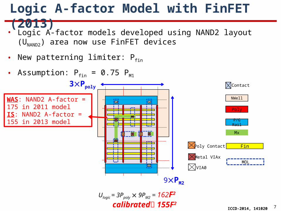
Logic A-factor Model with FinFET (2013)
3Ppoly
9PM2
Ulogic = 3Ppoly 9PM2 = 162F2
calibrated 155F2
• Logic A-factor models developed using NAND2 layout (UNAND2) area now use FinFET devices
• New patterning limiter: Pfin
• Assumption: Pfin = 0.75 PM1
Fin
MOLVIA0
Metal VIAx
Poly Contact
NWell
P/G Rail
Poly
Contact
Mx
WAS: NAND2 A-factor = 175 in 2011 modelIS: NAND2 A-factor = 155 in 2013 model
8ICCD-2014, 141020
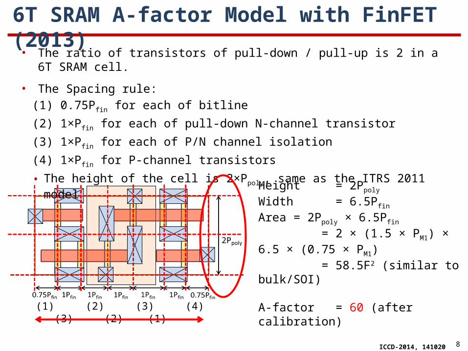
6T SRAM A-factor Model with FinFET (2013)
Height = 2Ppoly
Width = 6.5Pfin
Area = 2Ppoly × 6.5Pfin
= 2 × (1.5 × PM1) × 6.5 × (0.75 × PM1) = 58.5F2 (similar to bulk/SOI)
A-factor = 60 (after calibration)
• The ratio of transistors of pull-down / pull-up is 2 in a 6T SRAM cell.
• The Spacing rule:
(1) 0.75Pfin for each of bitline
(2) 1×Pfin for each of pull-down N-channel transistor
(3) 1×Pfin for each of P/N channel isolation
(4) 1×Pfin for P-channel transistors
• The height of the cell is 2×Ppoly, same as the ITRS 2011 model
(1) (2) (3) (4) (3) (2) (1)
9ICCD-2014, 141020
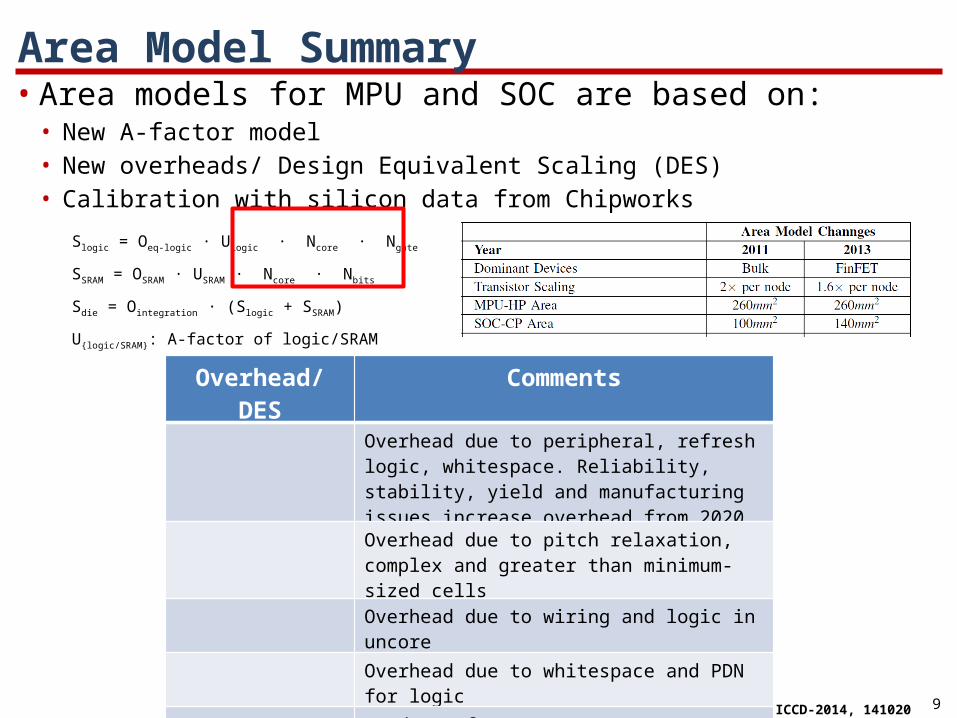
Area Model Summary• Area models for MPU and SOC are based on:
• New A-factor model• New overheads/ Design Equivalent Scaling (DES)• Calibration with silicon data from Chipworks
Slogic = Oeq-logic ∙ Ulogic ∙ Ncore ∙ Ngate
SSRAM = OSRAM ∙ USRAM ∙ Ncore ∙ Nbits
Sdie = Ointegration ∙ (Slogic + SSRAM)
U{logic/SRAM}: A-factor of logic/SRAM
Overhead/DES CommentsOverhead due to peripheral, refresh logic, whitespace. Reliability, stability, yield and manufacturing issues increase overhead from 2020
Overhead due to pitch relaxation, complex and greater than minimum-sized cells
Overhead due to wiring and logic in uncore
Overhead due to whitespace and PDN for logic
Product of , ,
Overhead due to whitespace, wiring of IP blocks, interfaces, etc.

10ICCD-2014, 141020
MPU Model Revision
SRAM1
SRAM2
SRAM3
SR
AM
5S
RA
M4
core1 core2
core3 core4
Accelerators
Memory Controller
I/O interfaces
GPUs
OintegrationOSRAM
Ologic
OAfactor-logic
Ouncore-logicKey components to address different densities and overheads:• Logic• SRAM• Uncore (new in 2013 model)
• New overheads• Ouncore-logic
• OAfactor-logic
• Calibrated Ointegration
• + Previous overheads• OSRAM
• Ologic
11ICCD-2014, 141020
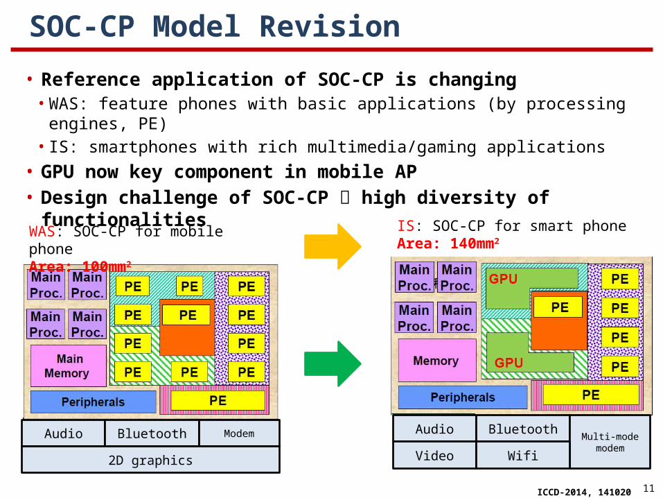
WAS: SOC-CP for mobile phoneArea: 100mm2
IS: SOC-CP for smart phoneArea: 140mm2
Audio Bluetooth Modem Audio BluetoothMulti-mode
modemVideo Wifi2D graphics
• Reference application of SOC-CP is changing• WAS: feature phones with basic applications (by processing engines, PE)• IS: smartphones with rich multimedia/gaming applications
• GPU now key component in mobile AP• Design challenge of SOC-CP high diversity of functionalities
SOC-CP Model Revision
12ICCD-2014, 141020
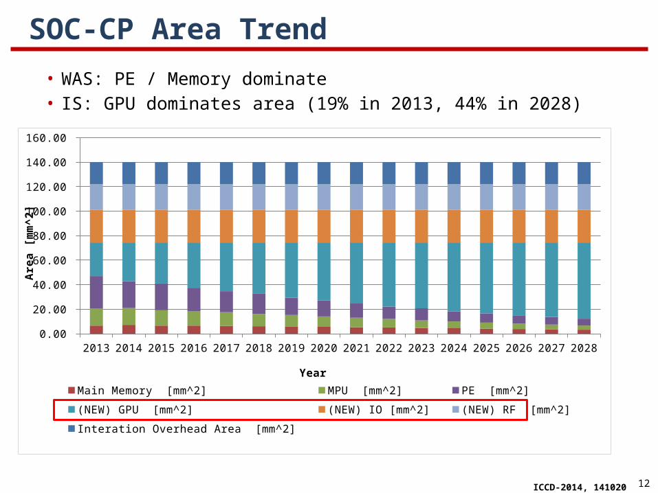
SOC-CP Area Trend
• WAS: PE / Memory dominate• IS: GPU dominates area (19% in 2013, 44% in 2028)
2013 2014 2015 2016 2017 2018 2019 2020 2021 2022 2023 2024 2025 2026 2027 20280.00
20.00
40.00
60.00
80.00
100.00
120.00
140.00
160.00
Main Memory [mm^2] MPU [mm^2] PE [mm^2] (NEW) GPU [mm^2] (NEW) IO [mm^2]
(NEW) RF [mm^2] Interation Overhead Area [mm^2]
Year
Are
a [m
m^2
]

13ICCD-2014, 141020
SOC-CP Performance Challenge• Performance requirement is extrapolated from historical demands• Available processing performance improvement
• Improved by faster devices• Improved by increasing #PE and GPUs
• Significant gap after 2015 calls out for desperate demand for architecture and design methodology improvements
Performancegap
{Processing performance} ={#main processors}×{main processor frequency}+{#GPUs}×{GPU frequency}
14ICCD-2014, 141020
Outline
• Overview of ITRS Design and System Drivers Chapters
• Architectural and Area Models of MPU and SOC• Design Capacity Gap and Design Equivalent
Scaling• Power Modeling and Power Management Gap• Conclusions
15ICCD-2014, 141020
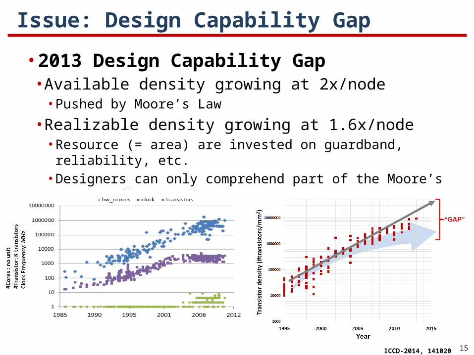
Issue: Design Capability Gap
• 2013 Design Capability Gap• Available density growing at 2x/node
• Pushed by Moore’s Law
• Realizable density growing at 1.6x/node• Resource (= area) are invested on guardband, reliability, etc.• Designers can only comprehend part of the Moore’s Law benefits

16ICCD-2014, 141020
20072008
20092010
20112012
20132014
20152016
20172018
20192020
20212022
20232024
20252026
20272028
0
1
2
3
4
5
6
7
8
9
10
11
Tran
sisto
r den
sity
(nor
mal
ized
to 2
007)
The “Design Capability Gap”
2x / node
22/3 ~1.587x / node
(1)
(2)
(1) AND (2)
(1) Uncore overheads(2) A-factor overheads
DESIGN CAPABILITY GAP!UCSD CSE Dept. Technical Report #CS2013-1002

17ICCD-2014, 141020
20072008
20092010
20112012
20132014
20152016
20172018
20192020
20212022
20232024
20252026
20272028
0
1
2
3
4
5
6
7
8
9
10
11
Tran
sisto
r den
sity
(nor
mal
ized
to 2
007)
The Design Equivalent Scaling
2x / node
22/3 ~1.587x / node
Design Equivalent Scaling: Recover the 2× per node scaling
for degraded 1.6 × per node

18ICCD-2014, 141020
Outline
• Overview of ITRS Design and System Drivers Chapters
• Architectural and Area Models of MPU and SOC• Design Capacity Gap and Design Equivalent
Scaling• Power Modeling and Power Management Gap• Conclusions

19ICCD-2014, 141020
Updates of Power SOC/MPU Models• Frequency roadmap keeps 1.04×/year• Device and BEOL parameters (e.g. gate/wire capacitance) are updated from
PIDS/INTC ITWGs• MPU-HP max frequency resets to 5.5GHz (↓)• SOC-CP max frequency (main processors) resets to 2.4GHz (↑)• The System Drivers working group defines multiple scenarios for SOC-CP power
model to reflect application-oriented power management
Year 2011 2013Power Scenario of MPU Single Scenario Single Scenario
Power Scenario of SOC Single Scenario Multiple Scenario
Frequency scaling of MPU and SOC
1.04x / year 1.04x /year
SOC-CP Max Frequency 1.37GHz@2013 2.4GHz@2013(main processors)
MPU-HP Max Frequency 7.34GHz@2013 5.5GHz@2013

20ICCD-2014, 141020
Scenario-based SOC-CP Power Model• Aggressive block-level power gating/frequency scaling are applied to
SOC-CP• We define four scenarios for applications and five categories of function
blocks• Total SOC-CP power for a scenario is the weighted sum of each function
block
Gaming: major long-term power challenge
Scenario-basedpower model

21ICCD-2014, 141020
Function Block-Based Frequency Roadmap
• (WAS) All function blocks scale at the same frequency• (IS) Each block scale the frequency separately
2013 2014 2015 2016 2017 2018 2019 2020 2021 2022 2023 2024 2025 2026 2027 20280.001.002.003.004.005.006.007.008.00
(IS) Main Processor [GHz](IS) GPU [GHz](IS) PE [GHz](WAS) Main Processor / PE / Peripheral [GHz]
Year
Freq
uenc
y [G
Hz]

22ICCD-2014, 141020
Scenario-Based SOC-CP Power Model• Dominant scenario: gaming with all 3D features
enabled • Large power gap beyond 2020• Low-power technologies (both device and design
technologies) will be required
Power requirement < 5W

23ICCD-2014, 141020
Outline
• Overview of ITRS Design and System Drivers Chapters
• Design Capacity Gap and Design Equivalent Scaling
• Architectural and Area Models of MPU and SOC• Power Modeling and Power Management Gap• Conclusions

24ICCD-2014, 141020
Conclusions• SRAM and logic A-factors are updated with new calibration• Area models are updated with new A-factor, and new
overhead models• Design Capability Gap stands between ideal density scaling
and actual (realized) density scaling• DES is required to restore the scaling to the Moore’s Law
track• Power model is updated with new frequency scaling, device
parameters, and new transistor density models• We have shown the low-power design challenge with the
scenario-based power model for SOC-CP

25ICCD-2014, 141020
Thank you!

26ICCD-2014, 141020
Backup
27ICCD-2014, 141020
Previous Challenge: Missing Node in Physical Scaling
2013
2014
2015
2016
2017
2018
2019
2020
2021
2022
2023
2024
2025
2026
2027
2028
200
250
300
350
400
450
WASIS (w/ 6y-DES)IS (w/o DES)
Year
Die
Are
a (m
m^2
)
• Problem• Metal pitch roadmap is slowed down from 2-year to 3-year cycle (one missing node from
2013)• Transistor density scales at 1.6per node die area explosion
• Solution: Design Equivalent Scaling• DES to recover one node of scaling from 2013 to 2019
• For MPU-HP and MPU-CP• DES to recover one node of scaling from 2013 to 2020
• For SOC-CP
Solution: Alt-1
One node missingMPU Area exploration
Rescued by DES
2013
2014
2015
2016
2017
2018
2019
2020
2021
2022
2023
2024
2025
2026
2027
2028
05
1015202530354045 WAS IS
Year
M1
HP
(F) (
nm)
Ideal Realistic
Solution: Alt-2

28ICCD-2014, 141020
Current 2014 ITRS Status
• (WAS, in our paper) missing scaling node from 2013
• (IS) Litho ITWG recovers the scaling to 0.5x/4 year
1
10
100
1000
1995 2000 2005 2010 2015 2020 2025 2030
Nan
om
eter
s (1
e-9)
Year of Production
2013 ITRS - Technology Trends
2013 ITRS MPU/ASIC Metal 1 (M1) ½ Pitch (contacted) (nm)
2013 ITRS MPU/ASIC Printed Gate Length (GLpr) (nm)
2013 ITRS MPU Physical Gate Length (GLph) (nm)
16nm
“Moore’s Law” Enabled byTransistor M1 Half Pitch Dimension Technology
Long-Term 21-28Near-Term 13-20
Transistor Gate TechnologyPower-performance Management Enabled by “Equivalent Scaling”
(IS) Litho ITWG recovers the scaling to 0.5x/4 year
(WAS, in the paper camera) missing node from 2013

29ICCD-2014, 141020
2014 SRAM A-factor Calibration• A-factor are calibrated with new silicon data• The updated 22nm/14nm silicon data indicate larger A-factor than that of previous nodes• For N10 (foundry node) SRAM, Design ITWG has the following updates:
• (WAS, 2013) SRAM A-factor was calibrated to 60• (WAS, 2013) Cell ratio (PU:PD:PG) = 1:2:1• (IS) SRAM A-factor is calibrated to 85• (IS) Cell ratio (PU:PD:PG) = 2:2:2
0102030405060700
10
20
30
40
50
60
70
80
90
100
SRAM A-factor vs. Node
Company-1Company-ACompany-BCompany-CCompany-5
Updated 22nm and 14nm data indicate higher SRAM A-factors than that of previous nodes
After considering new layout of FinFET SRAM, the A-factor is updated to 85 (2013: 60)
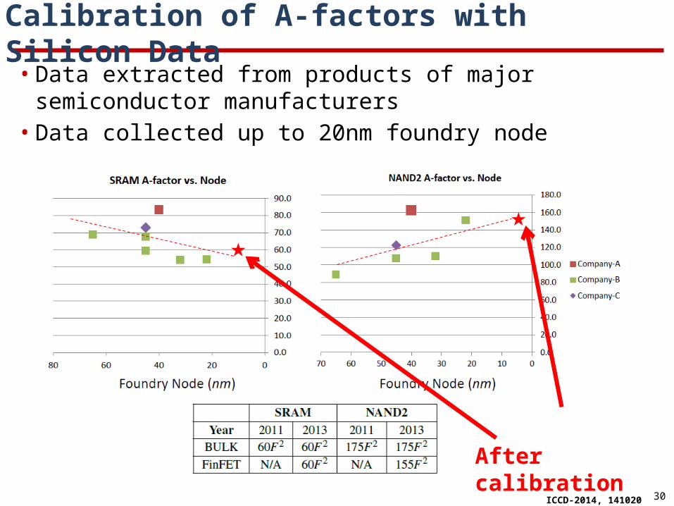
30ICCD-2014, 141020
Calibration of A-factors with Silicon Data• Data extracted from products of major semiconductor
manufacturers• Data collected up to 20nm foundry node
After calibration

31ICCD-2014, 141020
A-factor Density Model (2013)• Models of SRAM (USRAM) and NAND2 (UNAND2) area now use FinFET
• New patterning limiter: Pfin
• Assumption: Pfin = 0.75 PM1
USRAM = 2Ppoly 4.875PM1 = 58.5F2
calibrated 60F2
4.875PM1
2Ppoly
Fin
NWell
Poly
Contact

32ICCD-2014, 141020
A-factor Layout Model (2014)Alt-1: ITRS 2013 / Intel 22nm FinFET 6T SRAM (1:2:1)Assume Pfin = 0.75PM1
Assume Ppoly = 1.5PM1
Height = 2Ppoly
Width = 6.5Pfin
Area = 2Ppoly × 6.5Pfin
= 58.5F2 (similar to bulk)
A-factor = 60 (after calibration)
Alt-2: FinFET 6T SRAM (1:2:1) (Intel 14nm SRAM)
2Pfin 2Pfin 1Pfin1Pfin 0.75Pfin0.75Pfin
2Ppoly
2Pfin
Assume Pfin = 0.75PM1 Height = 2Ppoly
Width = 8.5Pfin
Area = 2Ppoly × 9.5Pfin
= 85F2
(Intel 14nm SRAM = 87F2)
PG
PD PG
PDPU
PU
PG
PG
PD
PD
PU
PU

33ICCD-2014, 141020
• http://www.itrs.net/
• 15-year technical outlook for 14 supplier industries and their respective technology areas
• 25-year projection of technology needs for emerging research devices and materials
• Drivers for world wide research and funding agencies• Organization divided (EU, Japan, Korea, Taiwan, USA), 1000+
participants• Neutrality with regard to commercial considerations
Mission of ITRS Roadmap

34ICCD-2014, 141020
Design & System Drivers
INTCCMP, R, C, MOL, Jmax
PIDSId,sat, Isd,leak
CV/I,fT
FEPV t variation
LITHO
Mask cost, CD 3σ,
pitch, overlay
Test
#cores, max IO freq
Interactions between ITWGs
ORTCs
• max chip power• layout density• transistor count• chip size• #distinct cores• #cores• max on-chip freq• product/market
drivers
Fundamental Models
A&P
#IOs, max power, thermal, TSV/3D roadmap

35ICCD-2014, 141020
Intel MPU Scaling Trends
[Sutter09]
# of Transistors
Clock Frequency
Power
Performance/CLK (ILP)
Related Documents