1 IC-Brazil Program created by MCT in 2005 Jacobus W. Swart CTI

1 IC-Brazil Program created by MCT in 2005 Jacobus W. Swart CTI.
Dec 14, 2015
Welcome message from author
This document is posted to help you gain knowledge. Please leave a comment to let me know what you think about it! Share it to your friends and learn new things together.
Transcript

1
IC-Brazil Program created by MCT in 2005
Jacobus W. SwartCTI

2
Outline Vision & Activities Organization Design houses Manufacturing Training HR Opportunities

Vision & Objectives To promote the development of an ecosystem in
microelectronics in Brazil and the insertion of Brazil in the semiconductor market
Promote local IC companies
Attraction of international companies
• E.g., Freescale – today 200 IC designers
• Smart - Back-end fabrication
Promote electronics innovation
Synergy with other governmental incentives:
• Informatics law
• PADIS – new program for semiconductors and displays
• Subvention programs by FINEP and BNDES

4
ActivitiesSupport for design houses
Support for fabrication:
• Wafer fabrication
• Packaging and
• Testing of IC´s
IC design training program

IC-Brazil Organization Steering Committee & 3 sub-committees
Infrastructure
Education
Business
Executive Office
Located at CTI, Campinas
5

6
Design Houses
7 Design Houses Already in Operation
C T Iwww.cti.gov.br
www.ceitec.org.br
www.cesar.org.br
www.lsitec.org.br
www.ctpim.org.br
www.vonbraunlabs.com.br
www.lincs.org.br

7
Design Houses Infrastructure
WorkstationsCadence's Software Tools
Cadence's Tool TrainingFellowships in the first years
Current 97 fellowships for 133 designersIC Design
IP LibraryComercial Designs: 19 finished & 18 in progress
Next steps: growth of existing DH´s and increase number to 15 DH´s until 2010

LINCS-CETENE
Team:25 designers5 trainees
Expertise:Modeling in System CDesign with Verilog-VHDL RTLFunctional verification using SCVPrototyping with FPGA (Altera)Silicon layout (Cadence)

LINCS - CETENE
PORTIFÓLIO
CAIP - Controle Automático de Iluminação PúblicaCAIP - Controle Automático de Iluminação Pública
www.lincs.org.br/chips
100% fi
rst t
ime
silic
on succ
ess
e
first p
rice a
t
IP/S
oC 2006.

Some Figures
√Human Resource – 25 designers
√ Infrastructure:
√ 400 m2 ( ~ 4500 sq ft) Lab area
√ 50 workstations
√ Tools: Cadence, Mentor Graphics, Altera, ...
Design House - CTI
Foundries Relationship√IBM BiCMOS technology 0,35um and 0,18um – Analog and RF√XFAB 1um, 0,6um, 0,35um and 0,18um – Analog, RF, HV (650V), Sensor and MEMs√Austriamicrosystems CMOS & BiCMOS 0,35um – Analog, RF√NEC – Structured ASICs
Technologies: √Mixed analog- digital IC design √Mixed RF and RFID√Mixed Smart Power√SoCs: FPGA and Structured ASICS
Projects & Services √Intelbras FINEP/VAEE√Intelbras FINEP/IPSVAEE √CIS Eletrônica FINEP/DECOD√ICs, Sensors, FPGAs, …
DHCTI

LSITEC
Analog & Mixed Mode Design
Digital ASIC / FPGA
www.lsitec.org.br
• 25 design engineers working in two offices:– Sao Paulo (SPO)– Salvador (SO, Bahia State)
• 70% with MsC or PhD• 2 Engineers have more than 15 years
experience in US design companies

IC Design
Signaling device, battery operated, to identify power interruptions in high power transmission lines
Outcome
Response Time to Repair has been reduced by 2/3
Mixed Mode IC developed in 3 months, from specs to tapeout Layout (left) and under test (right) Industrial production starts on April 2008 (using smd package)

13
Manufacturing Wafer fabrication:
foundriesCEITEC: 0.6 µm CMOS, start 2009
PackagingService providersCTI
Testing CTI and others
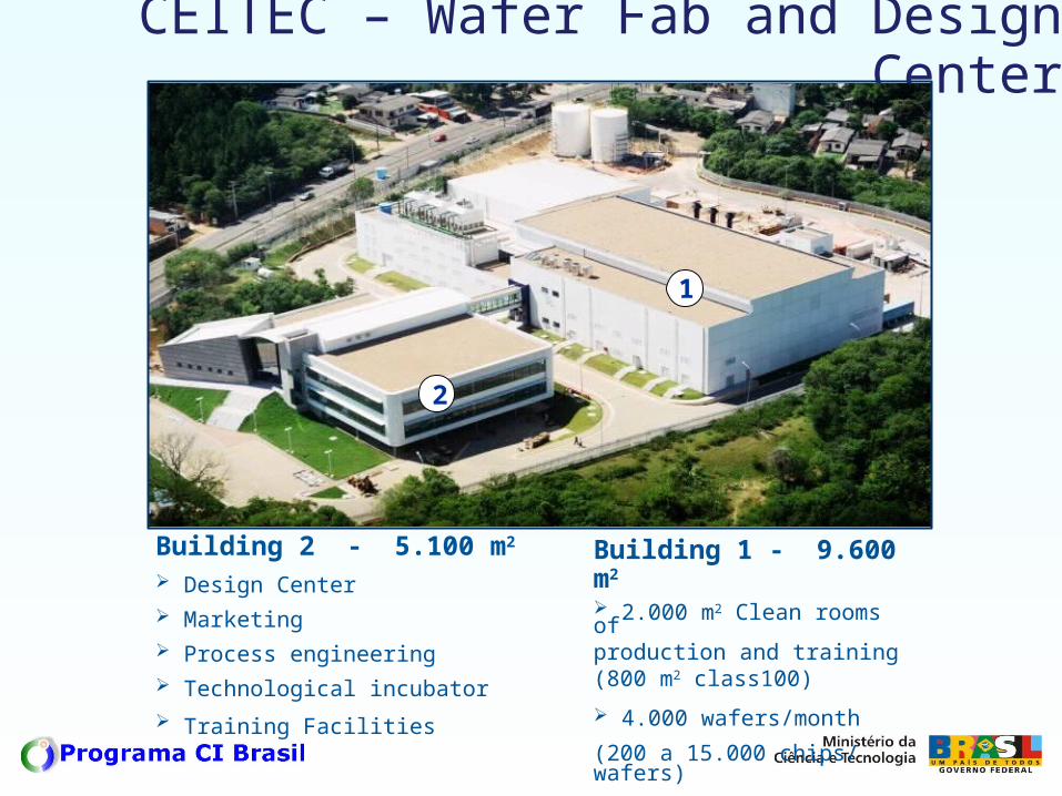
CEITEC – Wafer Fab and Design Center
Building 1 - 9.600 m2
2.000 m2 Clean rooms of production and training (800 m2 class100)
4.000 wafers/month
(200 a 15.000 chips/ wafers)
Building 2 - 5.100 m2
Design Center Marketing Process engineering Technological incubator
Training Facilities
1
2

Packaging at CTISmall scale ceramic packaging – engineering
phase of IC designChip on Board (COB) technology for
prototyping;Packaging of sensors and SAW devicesMicrosoldering of Al and Au wiresSpecial dicing for different substrates:
Si, GaAs, Al2O3, LiNbO3, glass, quartz, circuit boards, etc.

Optical Microscope
SEM w. EDX/WDS
Teradyne MicroFlex tester
Wafer prober – Micromanipulator 6400
Logic analyzer-HP16500B
FIB/SEM dual beam(@ CCS-UNICAMP)
Characterization and Failure Analysis

Burn-in Climatic chamber –
Vötsch 7033
Sample preparation
Thermal cycling
chamber Vötsch 7012
Reliability and Certification

18
Training Program Cadence's Partnership
1 Yr. Training Program (Digital, Analog & RF) Certification of Brazilian Instructors Objective ~ 1.500 designers in 3 to 4 years
First Training Centers in Porto Alegre and Campinas

19
Training Program 4 Training Centers
CT#1 – Porto Alegre, RS (Started on April 2008)CT#2 – Campinas, SP (Started on August 2008)CT#3 – TBD (On July 2009)CT#4 – TBD (On January 2010)
400 students per year from 2009 Phases
4 months – Theory & Tool Training8 months – Specific Commercial Project
Instructors & Training Content 1st year – Cadence's TeamTraining Content Designed by Cadence
Additional Training
Master & PhD programs in Brazil – estimate:
100 MSc + 40 PhD / year.
One year master program in France:
university & ST Microelectronics – 12 students
/ year
On the job training at Freescale: 24 engineers

21
Opportunities DHs have strong demand for designers
In the Training Centers
Lectures
Instructors
Lab Assistants
Team Leaders
New Network Program: SIBRATEC
Microelectronics
Electronics Products Quality
Photovoltaics
22
Financial Support

Centro de Tecnologia da Informação Renato Archer
www.ci-brasil.gov.br
Figures:Campus area
= 320.000 m2
Building area = 14.000 m2
People = 300
Related Documents